Page 1
Summit Data Communications, Inc., 526 South Main Street Suite 805 Akron, OH 44311 Tel: 866-434-4300 www.summitdatacom.com
© 2011 – 2012 Summit Data Communications, Inc. All rights reserved.
SDC-SSD40NBT
User’s Guide
Page 2
Hardware Integration Guide – SDC-SSD40NBT
2 SDC-SSD40NBT_UsersGuide
© 2011 – 2012 Summit Data Communications, Inc. All rights reserved.
Contents
Contents ........................................................................................................................................................ 2
Scope ............................................................................................................................................................. 3
Operational Description ................................................................................................................................ 3
Specifications ................................................................................................................................................ 5
Recommended Operating Conditions and DC Electrical Characteristics ............................................ 11
SDIO Timing Requirements ................................................................................................................. 12
UART Timing Requirements ................................................................................................................ 13
PCM Interface Timing .......................................................................................................................... 13
Control Signal Timing Requirements .................................................................................................. 18
Pin Definitions ............................................................................................................................................. 19
SSD30AG and SSD40NBT Pin Comparison Table ................................................................................. 23
Electrical Considerations ..................................................................................................................... 24
Integration Considerations ................................................................................................................. 25
Mechanical Specifications ........................................................................................................................... 26
Mounting................................................................................................................................................. 28
RF Layout Design Guidelines ....................................................................................................................... 29
Regulatory ................................................................................................................................................... 30
Certified Antennas .................................................................................................................................. 30
Documentation Requirements ............................................................................................................... 31
FCC ......................................................................................................... Error! Bookmark not defined.
Industry Canada ..................................................................................... Error! Bookmark not defined.
European Union .................................................................................................................................. 32
Page 3
Hardware Integration Guide – SDC-SSD40NBT
3 SDC-SSD40NBT_UsersGuide
© 2011 – 2012 Summit Data Communications, Inc. All rights reserved.
Scope
This document describes key hardware aspects of the Summit SSD40NBT radio module. This document
is intended to assist device manufacturers and related parties with the integration of this radio into their
host devices. Data in this document are drawn from a number of sources and include information found in
the Broadcom BCM4329data sheet issued in June of 2009.
The SDC-SSD40NBT is currently in pre-production and as such, this document is preliminary; the
information in this document is subject to change. Please contact Summit or visit the Summit website at
www.summitdatacom.com to obtain the most recent version of this document.
Operational Description
This device is an SDC-SSD40NBT radio module which supports IEEE
802.11a/b/g/n standards via an SDIO (Secure Digital Input/Output)
interface and Bluetooth version 2.1 via a serial UART (Universal
Asynchronous Receiver/Transmitter) interface. The radio operates in
unlicensed portions of the 2.4 GHz and 5 GHz radio frequency
spectrum. The device is compliant with IEEE 802.11a,
802.11b,802.11g, and 802.11n standards using Direct Sequence
Spread Spectrum (DSSS), Orthogonal Frequency Division Multiplexing
(OFDM), and supports Bluetooth 2.1 using Frequency Hopping Spread
Spectrum (FHSS). The device supports all 802.11a, 802.11b, 802.11g,
802.11n, and Bluetooth data rates and automatically adjusts data rates and operational modes based on
various environmental factors.
When operating on channels in the UNII-2 and UNII-2 Extended bands that are in the 5GHz portion of the
frequency spectrum and are subject to Dynamic Frequency Selection requirements, the SDC-SSD40NBT
fully conforms to applicable regulatory requirements. In the event that specified types of radar are
detected by the network infrastructure, the SDC-SSD40NBT fully conforms to commands from the
infrastructure for radar avoidance.
The SDC-SSD40NBTis a System in Package (SiP) Quad Flat pack, No leads (QFN) module and
interfaces to host devices via a 56-padedge connector. The device is based on the Broadcom
BCM4329chip which is an integrated device providing a Media Access Controller (MAC), a Physical Layer
Controller (PHY or baseband processor), and fully integrated dual-band radio transceiver. To maximize
operational range, the SDC-SSD40NBT incorporates a 5 GHz power amplifier (PA) to increase transmit
power. The frequency stability for both 2.4 GHz (802.11b and 802.11g) and 5 GHz (802.11a) operation is
+/- 20 ppm.
The SSD40NBT has its own RF shielding and does not require shielding provided by the host device into
which it is installed in order to maintain compliance with applicable regulatory standards. As such, the
device may be tested in a standalone configuration via an extender card.
The device buffers all data inputs so that it will comply with all applicable regulations even in the presence
of over-modulated input from the host device. Similarly, the SDC-SSD40NBT incorporates power
regulation to comply with all applicable regulations even when receiving excess power from the host
device.
Page 4
Hardware Integration Guide – SDC-SSD40NBT
4 SDC-SSD40NBT_UsersGuide
© 2011 – 2012 Summit Data Communications, Inc. All rights reserved.
The SDC-SSD40NBT provides two diplexed antenna interfaces to support dual band transmit and receive
diversity. Supported host device antenna types include dipole and monopole antennas.
Note: When using a single antenna, it must be connected to the AUX port. BT does not function on the
Main port alone.
Regulatory operational requirements are included with this document and may be incorporated into the
operating manual of any device into which the SDC-SSD40NBT is installed. The SDC-SSD40NBT is
designed for installation into mobile devices such as vehicle mount data terminals (which typically operate
at distances greater than 20 cm from the human body) and portable devices such as handheld data
terminals (which typically operate at distances less than 20 cm from the human body). See
“Documentation Requirements” for more information.
Page 5
Hardware Integration Guide – SDC-SSD40NBT
5 SDC-SSD40NBT_UsersGuide
© 2011 – 2012 Summit Data Communications, Inc. All rights reserved.
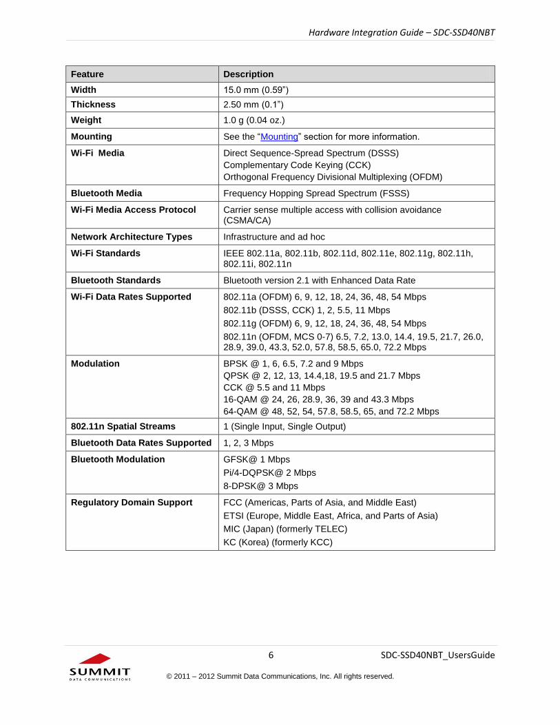
Specifications
Feature Description
Physical Interface 0.4mm pitch QFN (Quad Flat Pack, No Leads)
Wi-Fi Interface 1-bit or 4-bit Secure Digital I/O
Bluetooth Interface Host Controller Interface (HCI) using High Speed UART
Main Chip Broadcom BCM4329
Input Voltage Requirements 3.3 VDC ± 10% (core)
I/O Signaling Voltage 1.8 to 3.3 VDC ± 10%
Average Current Consumption,
VDDIO = 3.3 volts
(At maximum transmit power
setting)
Note: Standby refers to the radio
operating in PM1
powersave mode.
802.11a (with BT in standby)
Transmit: 282 mA (931 mW)
Receive: 92 mA (304 mW)
Standby: TBD
802.11b (with BT in standby)
Transmit: 314 mA (1036 mW)
Receive: 92 mA (304 mW)
Standby: TBD
802.11g (with BT in standby)
Transmit: 288 mA (950 mW)
Receive: 92 mA (304 mW)
Standby: TBD
802.11n (2.4 GHz) (with BT in standby)
Transmit: 292 mA (964 mW)
Receive: 92 mA (304 mW)
Standby: TBD
802.11n (5 GHz) (with BT in standby)
Transmit: 270 mA (891 mW)
Receive: 92 mA (304 mW)
Standby: TBD
Bluetooth (with Wi-Fi in standby)
Transmit: TBD
Receive: TBD
Operating Temperature -25° to 80°C (-22° to 176°F)
Operating Humidity 10 to 90% (non-condensing)
Storage Temperature -30° to 85°C (-22° to 185°F)
Storage Humidity 10 to 90% (non-condensing)
Maximum Electrostatic Discharge
8 kV
Length 15.0 mm (0.59”)
Page 6
Hardware Integration Guide – SDC-SSD40NBT
6 SDC-SSD40NBT_UsersGuide
© 2011 – 2012 Summit Data Communications, Inc. All rights reserved.
Feature Description
Width 15.0 mm (0.59”)
Thickness 2.50 mm (0.1”)
Weight 1.0 g (0.04 oz.)
Mounting See the “Mounting” section for more information.
Wi-Fi Media Direct Sequence-Spread Spectrum (DSSS)
Complementary Code Keying (CCK)
Orthogonal Frequency Divisional Multiplexing (OFDM)
Bluetooth Media Frequency Hopping Spread Spectrum (FSSS)
Wi-Fi Media Access Protocol Carrier sense multiple access with collision avoidance (CSMA/CA)
Network Architecture Types Infrastructure and ad hoc
Wi-Fi Standards IEEE 802.11a, 802.11b, 802.11d, 802.11e, 802.11g, 802.11h, 802.11i, 802.11n
Bluetooth Standards Bluetooth version 2.1 with Enhanced Data Rate
Wi-Fi Data Rates Supported 802.11a (OFDM) 6, 9, 12, 18, 24, 36, 48, 54 Mbps
802.11b (DSSS, CCK) 1, 2, 5.5, 11 Mbps
802.11g (OFDM) 6, 9, 12, 18, 24, 36, 48, 54 Mbps
802.11n (OFDM, MCS 0-7) 6.5, 7.2, 13.0, 14.4, 19.5, 21.7, 26.0, 28.9, 39.0, 43.3, 52.0, 57.8, 58.5, 65.0, 72.2 Mbps
Modulation BPSK @ 1, 6, 6.5, 7.2 and 9 Mbps
QPSK @ 2, 12, 13, 14.4,18, 19.5 and 21.7 Mbps
CCK @ 5.5 and 11 Mbps
16-QAM @ 24, 26, 28.9, 36, 39 and 43.3 Mbps
64-QAM @ 48, 52, 54, 57.8, 58.5, 65, and 72.2 Mbps
802.11n Spatial Streams 1 (Single Input, Single Output)
Bluetooth Data Rates Supported 1, 2, 3 Mbps
Bluetooth Modulation GFSK@ 1 Mbps
Pi/4-DQPSK@ 2 Mbps
8-DPSK@ 3 Mbps
Regulatory Domain Support FCC (Americas, Parts of Asia, and Middle East)
ETSI (Europe, Middle East, Africa, and Parts of Asia)
MIC (Japan) (formerly TELEC)
KC (Korea) (formerly KCC)
Page 7
Hardware Integration Guide – SDC-SSD40NBT
7 SDC-SSD40NBT_UsersGuide
© 2011 – 2012 Summit Data Communications, Inc. All rights reserved.
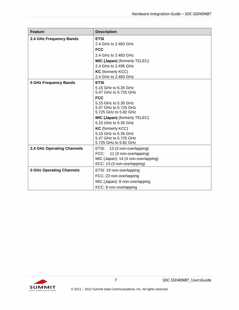
Feature Description
2.4 GHz Frequency Bands ETSI
2.4 GHz to 2.483 GHz
FCC
2.4 GHz to 2.483 GHz
MIC (Japan) (formerly TELEC)
2.4 GHz to 2.495 GHz
KC (formerly KCC)
2.4 GHz to 2.483 GHz
5 GHz Frequency Bands ETSI
5.15 GHz to 5.35 GHz 5.47 GHz to 5.725 GHz
FCC
5.15 GHz to 5.35 GHz 5.47 GHz to 5.725 GHz 5.725 GHz to 5.82 GHz
MIC (Japan) (formerly TELEC)
5.15 GHz to 5.35 GHz
KC (formerly KCC)
5.15 GHz to 5.35 GHz 5.47 GHz to 5.725 GHz 5.725 GHz to 5.82 GHz
2.4 GHz Operating Channels ETSI: 13 (3 non-overlapping)
FCC: 11 (3 non-overlapping)
MIC (Japan): 14 (4 non-overlapping)
KCC: 13 (3 non-overlapping)
5 GHz Operating Channels ETSI: 19 non-overlapping
FCC: 23 non-overlapping
MIC (Japan): 8 non-overlapping
KCC: 8 non-overlapping
Page 8
Hardware Integration Guide – SDC-SSD40NBT
8 SDC-SSD40NBT_UsersGuide
© 2011 – 2012 Summit Data Communications, Inc. All rights reserved.
Feature Description
Transmit Power
Note: Transmit power varies according to individual country regulations. All values nominal, +/-2 dBm.
Note: Summit 40 series radios support a single spatial stream and 20 MHz channels only.
802.11a
6 Mbps 16 dBm (40 mW)
54 Mbps 16 dBm (40 mW)
802.11b
1 Mbps 16 dBm (40 mW)
11 Mbps 16 dBm (40 mW)
802.11g
6 Mbps 15 dBm (32 mW)
54 Mbps 14 dBm (25 mW)
802.11n (2.4 GHz)
6.5 Mbps (MCS0) 13 dBm (40 mW)
65 Mbps (MCS7) 11 dBm (13 mW)
802.11n (5 GHz)
6.5 Mbps (MCS0) 16 dBm (40 mW)
65 Mbps (MCS7) 13 dBm (20 mW)
Bluetooth
1 Mbps -0.5 dBm (1.1 mW) 2 Mbps -0.5 dBm (1.1 mW) 3 Mbps -0.5 dBm (1.1 mW)
Typical Receiver Sensitivity
Note: All values nominal, +/-3 dBm.
802.11a:
6 Mbps -89 dBm 54 Mbps -77 dBm (PER <= 10%)
802.11b:
1 Mbps -95 dBm 11 Mbps -87 dBm (PER <= 8%)
802.11g:
6 Mbps -90 dBm
54 Mbps -77 dBm (PER <= 10%)
802.11n (2.4 GHz)
MCS0 Mbps -90 dBm MCS7 Mbps -73 dBm
802.11n (5 GHz)
MCS0 Mbps MCS7 Mbps
-88 dBm -71 dBm
Bluetooth:
1 Mbps TBD 2 Mbps TBD 3 Mbps TBD
Operating Systems Supported Windows Mobile 6.5
Windows Mobile 6.1
Windows Mobile 6.0
Windows Mobile 5.0
Windows Embedded CE 7.0
Page 9
Hardware Integration Guide – SDC-SSD40NBT
9 SDC-SSD40NBT_UsersGuide
© 2011 – 2012 Summit Data Communications, Inc. All rights reserved.
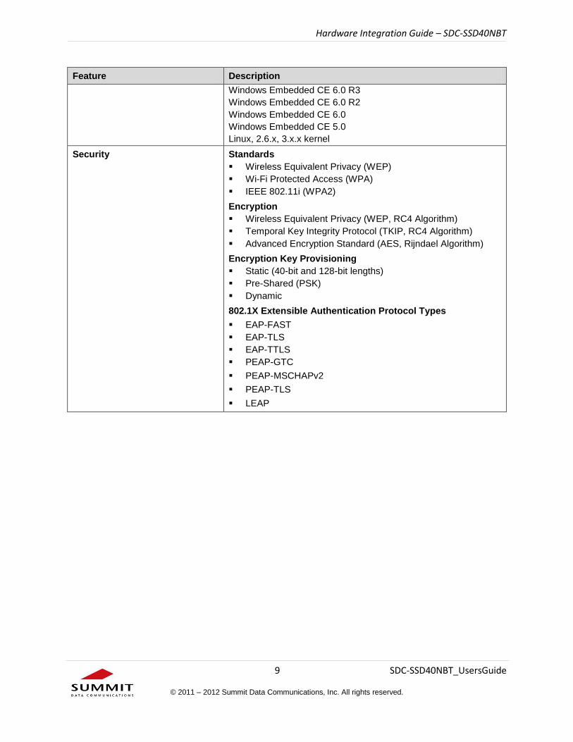
Feature Description
Windows Embedded CE 6.0 R3
Windows Embedded CE 6.0 R2
Windows Embedded CE 6.0
Windows Embedded CE 5.0
Linux, 2.6.x, 3.x.x kernel
Security Standards
Wireless Equivalent Privacy (WEP)
Wi-Fi Protected Access (WPA)
IEEE 802.11i (WPA2)
Encryption
Wireless Equivalent Privacy (WEP, RC4 Algorithm)
Temporal Key Integrity Protocol (TKIP, RC4 Algorithm)
Advanced Encryption Standard (AES, Rijndael Algorithm)
Encryption Key Provisioning
Static (40-bit and 128-bit lengths)
Pre-Shared (PSK)
Dynamic
802.1X Extensible Authentication Protocol Types
EAP-FAST
EAP-TLS
EAP-TTLS
PEAP-GTC
PEAP-MSCHAPv2
PEAP-TLS
LEAP
Page 10
Hardware Integration Guide – SDC-SSD40NBT
10 SDC-SSD40NBT_UsersGuide
© 2011 – 2012 Summit Data Communications, Inc. All rights reserved.
Feature Description
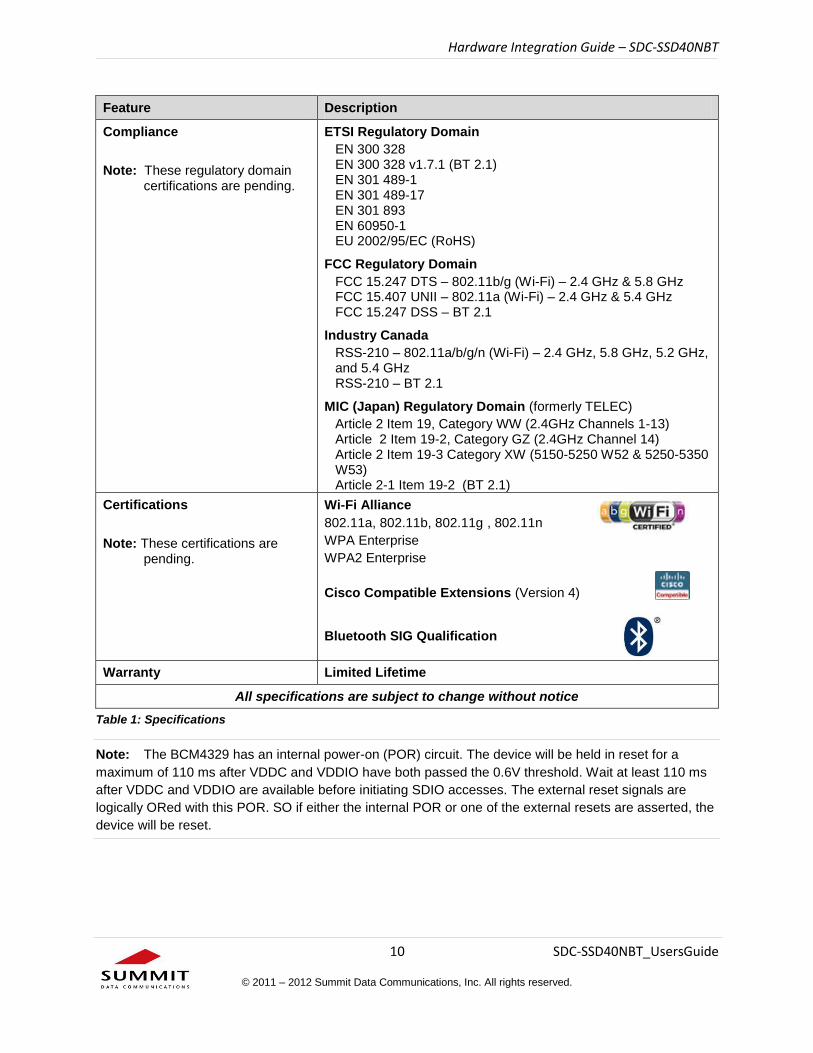
Compliance
Note: These regulatory domain certifications are pending.
ETSI Regulatory Domain
EN 300 328 EN 300 328 v1.7.1 (BT 2.1) EN 301 489-1 EN 301 489-17 EN 301 893 EN 60950-1 EU 2002/95/EC (RoHS)
FCC Regulatory Domain
FCC 15.247 DTS – 802.11b/g (Wi-Fi) – 2.4 GHz & 5.8 GHz FCC 15.407 UNII – 802.11a (Wi-Fi) – 2.4 GHz & 5.4 GHz FCC 15.247 DSS – BT 2.1
Industry Canada
RSS-210 – 802.11a/b/g/n (Wi-Fi) – 2.4 GHz, 5.8 GHz, 5.2 GHz, and 5.4 GHz RSS-210 – BT 2.1
MIC (Japan) Regulatory Domain (formerly TELEC)
Article 2 Item 19, Category WW (2.4GHz Channels 1-13) Article 2 Item 19-2, Category GZ (2.4GHz Channel 14) Article 2 Item 19-3 Category XW (5150-5250 W52 & 5250-5350 W53) Article 2-1 Item 19-2 (BT 2.1)
Certifications
Note: These certifications are pending.
Wi-Fi Alliance
802.11a, 802.11b, 802.11g , 802.11n
WPA Enterprise
WPA2 Enterprise
Cisco Compatible Extensions (Version 4)
Bluetooth SIG Qualification
Warranty Limited Lifetime
All specifications are subject to change without notice
Table 1: Specifications
Note: The BCM4329 has an internal power-on (POR) circuit. The device will be held in reset for a
maximum of 110 ms after VDDC and VDDIO have both passed the 0.6V threshold. Wait at least 110 ms
after VDDC and VDDIO are available before initiating SDIO accesses. The external reset signals are
logically ORed with this POR. SO if either the internal POR or one of the external resets are asserted, the
device will be reset.
Page 11
Hardware Integration Guide – SDC-SSD40NBT
11 SDC-SSD40NBT_UsersGuide
© 2011 – 2012 Summit Data Communications, Inc. All rights reserved.
Recommended Operating Conditions and DC Electrical Characteristics
Symbol Parameter Min Typ Max Unit
VCC DC Supply Voltage 3.0 3.3 3.6 V
VDD_IO DC Supply Voltage (I/O) 1.8 - 3.3 V
VIL Low Level Input Voltage (VDDO = 3.3V)
- - 0.8 V
VIH High Level Input Voltage (VDDO = 3.3V)
2.0 - - V
VIL Low Level Input Voltage (VDDO = 1.8V)
- - 0.6 V
VIH High Level Input Voltage (VDDO = 1.8V)
1.1 - - V
VOL Low Level Output Voltage (100 µA load)
- - 0.2 V
VOH High Level Output Voltage (-100 µA load)
VDDIO – 0.2V
- - V
IIL Low Current Input - 0.3 - µA
IIH High Current Input - 0.3 - µA
IOL Low Current Output (VDDO = 3.3V, VOL = 0.4V)
- - 3.0 mA
IOH High Current Output (VDDO = 3.3V, VOH = 2.9V)
- - 3.0 mA
CIN Input Capacitance - - 5 pF
BT UART Baud Rate 9600 bps
115.2 Kbps
(default coming out
of reset)
4 Mbps bps/Kbps/Mbps
Table 2: Recommended Operating Conditions and DC Electrical Characteristics
Page 12
Hardware Integration Guide – SDC-SSD40NBT
12 SDC-SSD40NBT_UsersGuide
© 2011 – 2012 Summit Data Communications, Inc. All rights reserved.
SDIO Timing Requirements
The following figure (Figure 2) and table display SDIO default mode timing.
Figure 1: SDIO Default Mode Timing
Note: Timing is based on CL ≤ 40pF load on CMD and Data.
Symbol Parameter Min Typ Max Unit
SDIO CLK (All values are referred to minimum VIH and maximum VIL*)
fPP Frequency – Data Transfer mode 0 - 25 MHz
fOD Frequency – Identification mode 0 - 400 kHz
tWL Clock low time 10 - - ns
tWH Clock high time 10 - - ns
tTLH Clock rise time - - 10 ns
tTHL Clock low time - - 10 ns
Inputs: CMD, DAT (referenced to CLK)
tISU Input setup time 5 - - ns
tIH Input hold time 5 - - ns
Outputs: CMD, DAT (referenced to CLK)
tODLY Output delay time – Data Transfer mode 0 - 14 ns
tODLY Output delay time – Identification mode 0 - 50 ns
* min(Vih) = 0.7 x VDDIO and max(ViL) = 0.2 x VDDIO.
Table 3: SDIO Timing Requirements
Page 13
Hardware Integration Guide – SDC-SSD40NBT
13 SDC-SSD40NBT_UsersGuide
© 2011 – 2012 Summit Data Communications, Inc. All rights reserved.
UART Timing Requirements
The following figure (Figure 3) displays UART timing.
Figure 2: UART Timing Requirements
Notes: The UART 4-wire interface supports Bluetooth 2.1 HCI Specification.
Reference Description Min. Typ. Max. Unit
1 Delay time, BT_UART_CTS_N low to UART_TXD valid
- - 24 Baudout cycles
2 Setup time, BT_UART_CTS_N high before midpoint of stop bit
- - 10 ns
3 Delay time, midpoint of stop bit to BT_UART_RTS_N high
- - 2 Baudout cycles
Table 4: UART Timing Requirements
PCM Interface Timing
PCM Defaults
Short Frame Sync, Master Mode
Short Frame Sync, Slave Mode
Long Frame Sync, Master Mode
Long Frame Sync, Slave Mode
PCM Defaults
SCO Routing PCM Interface Rate 512
Clock Mode Master Sample Interval 8khz
Sync Mode Master 16 bit mono
Frame Type Short
Page 14
Hardware Integration Guide – SDC-SSD40NBT
14 SDC-SSD40NBT_UsersGuide
© 2011 – 2012 Summit Data Communications, Inc. All rights reserved.
Short Frame Sync, Master Mode
Figure 3: Short Frame Sync, Master Mode
Reference Description Min. Typ. Max. Unit
1 PCM bit clock frequency 128 - 2048 kHz
2 PCM bit clock high time 128 - - ns
3 PCM bit clock low time 209 - - ns
4 Delay from BT_PCM_CLK rising edge to BT_PCM_SYNC high
- - 50 ns
5 Delay from BT_PCM_CLK rising edge to BT_PCM_SYNC low
- - 50 ns
6 Delay from BT_PCM_CLK rising edge to data valid on BT_PCM_OUT
- - 50 ns
7 Setup time for BT_PCM_IN before BT_PCM_CLK falling edge
50 - - ns
8 Hold time for BT_PCM_IN after BT_PCM_CLK falling edge
10 - - ns
9
Delay from falling edge of BT_PCM_CLK during last bit period to BT_PCM_OUT becoming high impedance
- - 50 ns
Table 5: Short Frame Sync, Master Mode
Page 15
Hardware Integration Guide – SDC-SSD40NBT
15 SDC-SSD40NBT_UsersGuide
© 2011 – 2012 Summit Data Communications, Inc. All rights reserved.
Short Frame Sync, Slave Mode
Figure 4: Short Frame Sync, Slave Mode
Reference Description Min. Typ. Max. Unit
1 PCM bit clock frequency 128 - 2048 kHz
2 PCM bit clock high time 209 - - ns
3 PCM bit clock low time 209 - - ns
4 Setup time for BT_PCM_SYNC before falling edge of BT_PCM_BCLK
50 - - ns
5 Hold time for BT_PCM_SYNC after falling edge of BT_PCM_CLK
10 - - ns
6 Hold time of BT_PCM_OUT after BT_PCM_CLK falling time
- - 175 ns
7 Setup time for BT_PCM_IN before BT_PCM_CLK falling edge
50 - - ns
8 Hold time for BT_PCM_IN after BT_PCM_CLK falling edge
10 - - ns
9
Delay from falling edge of BT_PCM_CLK during last bit period to BT_PCM_OUT becoming high impedance
- - 100 ns
Table 6: Short Frame Sync, Slave Mode
Page 16
Hardware Integration Guide – SDC-SSD40NBT
16 SDC-SSD40NBT_UsersGuide
© 2011 – 2012 Summit Data Communications, Inc. All rights reserved.
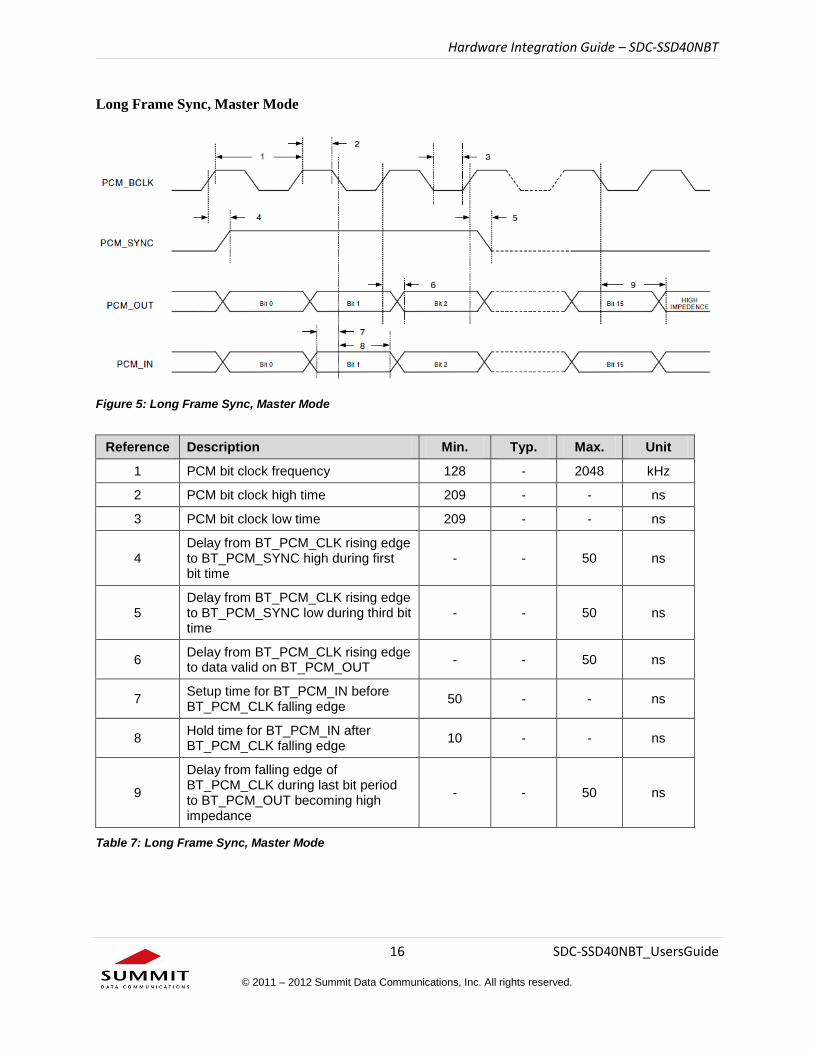
Long Frame Sync, Master Mode
Figure 5: Long Frame Sync, Master Mode
Reference Description Min. Typ. Max. Unit
1 PCM bit clock frequency 128 - 2048 kHz
2 PCM bit clock high time 209 - - ns
3 PCM bit clock low time 209 - - ns
4 Delay from BT_PCM_CLK rising edge to BT_PCM_SYNC high during first bit time
- - 50 ns
5 Delay from BT_PCM_CLK rising edge to BT_PCM_SYNC low during third bit time
- - 50 ns
6 Delay from BT_PCM_CLK rising edge to data valid on BT_PCM_OUT
- - 50 ns
7 Setup time for BT_PCM_IN before BT_PCM_CLK falling edge
50 - - ns
8 Hold time for BT_PCM_IN after BT_PCM_CLK falling edge
10 - - ns
9
Delay from falling edge of BT_PCM_CLK during last bit period to BT_PCM_OUT becoming high impedance
- - 50 ns
Table 7: Long Frame Sync, Master Mode
Page 17
Hardware Integration Guide – SDC-SSD40NBT
17 SDC-SSD40NBT_UsersGuide
© 2011 – 2012 Summit Data Communications, Inc. All rights reserved.
Long Frame Sync, Slave Mode
Figure 6: Long Frame Sync, Slave Mode
Reference Description Min. Typ. Max. Unit
1 PCM bit clock frequency 128 - 2048 kHz
2 PCM bit clock high time 209 - - ns
3 PCM bit clock low time 209 - - ns
4 Setup time for BT_PCM_SYNC before falling edge of BT_PCM_CLK during first bit time
50 - - ns
5
Hold time for BT_PCM_SYNC after falling edge of BT_PCM_CLK during second bit period.
Note: BT_PCM_SYNC may go low any time from second bit period to last bit period.
10 - - ns
6
Delay from rising edge of BT_PCM_CLK or BT_PCM_SYNC (whichever is later) to data valid for first bit on BT_PCM_OUT
- - 50 ns
7 Hold time of BT_PCM_OUT after BT_PCM_CLK falling edge
- - 175 ns
8 Setup time for BT_PCM_IN before BT_PCM_CLK falling edge
50 - - ns
9 Hold time for BT_PCM_IN after BT_PCM_CLK falling edge
10 - - ns
Page 18
Hardware Integration Guide – SDC-SSD40NBT
18 SDC-SSD40NBT_UsersGuide
© 2011 – 2012 Summit Data Communications, Inc. All rights reserved.
Reference Description Min. Typ. Max. Unit
10
Delay from falling edge of BT_PCM_CLK or BT_PCM_SYNC (whichever is later) during last bit in slot to BT_PCM_OUT becoming high impedence
- - 100
Table 8: Long Frame Sync, Slave Mode
Control Signal Timing Requirements
The following figure (Figure 4) displays Control Signal timing.
Figure 4: Control Signal Timing WLAN = ON, Bluetooth = ON
Note: This radio has an integrated power-on reset circuit that resets all circuits to a known power-on
state. Individual resets can also be driven by BT_RST_N or SYS_RST_N (an active-low, external reset
signal which can be used to externally force the device into a power-on reset state)
Page 19
Hardware Integration Guide – SDC-SSD40NBT
19 SDC-SSD40NBT_UsersGuide
© 2011 – 2012 Summit Data Communications, Inc. All rights reserved.
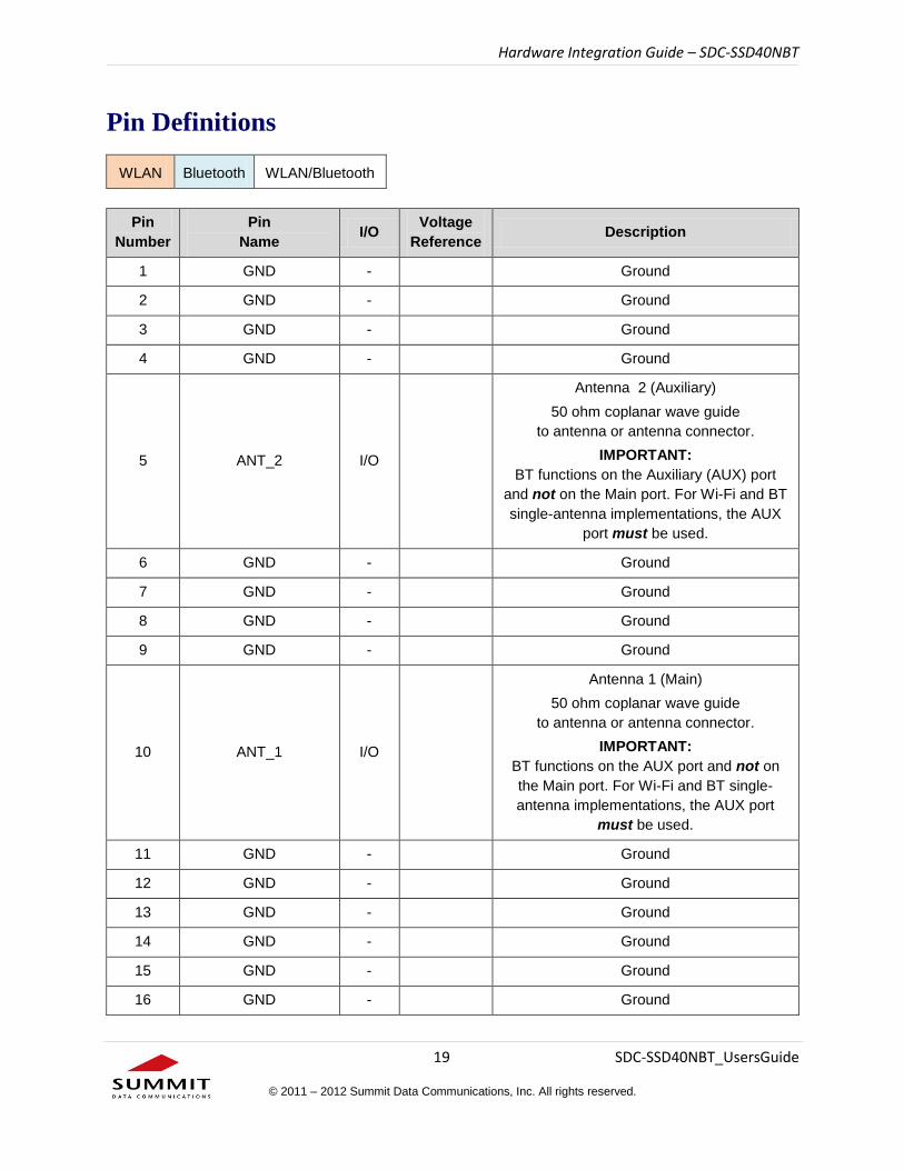
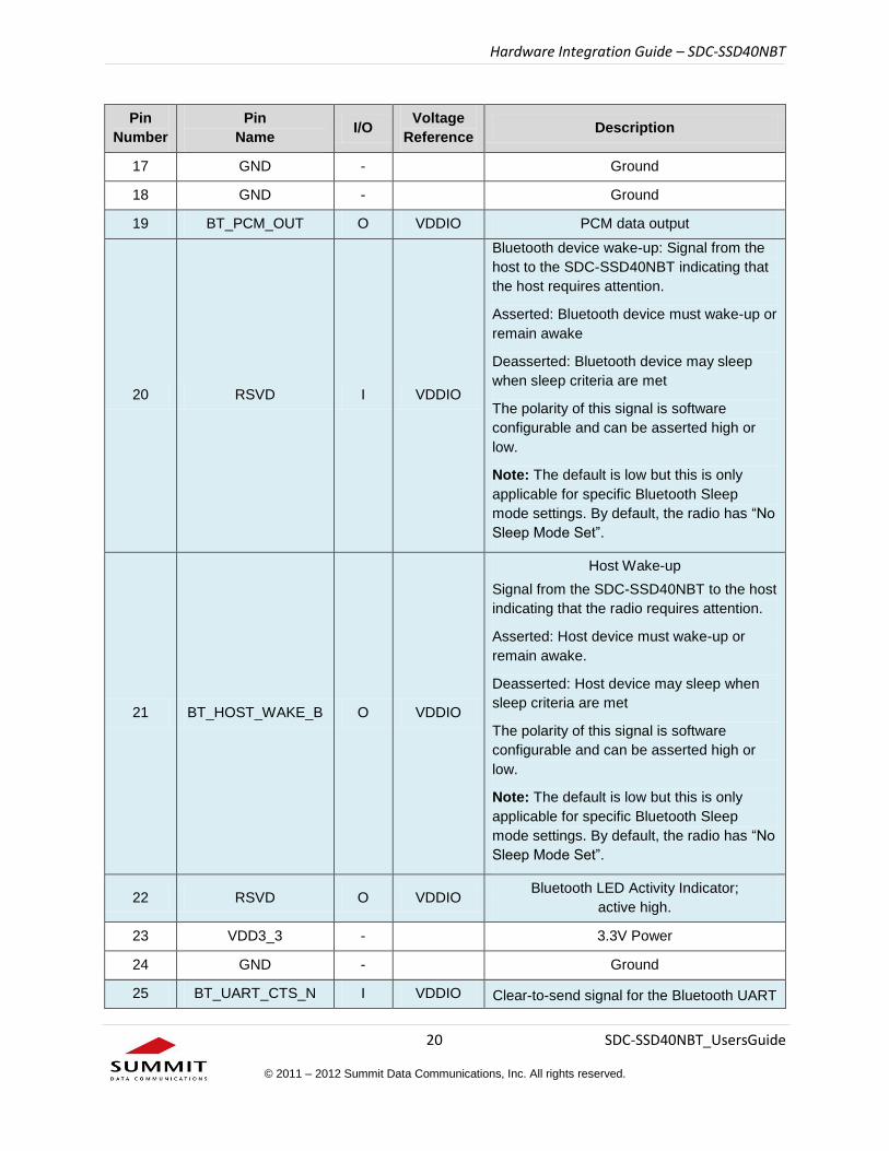
Pin Definitions
WLAN Bluetooth WLAN/Bluetooth
Pin
Number
Pin
Name I/O
Voltage
Reference Description
1 GND - Ground
2 GND - Ground
3 GND - Ground
4 GND - Ground
5 ANT_2 I/O
Antenna 2 (Auxiliary)
50 ohm coplanar wave guide
to antenna or antenna connector.
IMPORTANT:
BT functions on the Auxiliary (AUX) port
and not on the Main port. For Wi-Fi and BT
single-antenna implementations, the AUX
port must be used.
6 GND - Ground
7 GND - Ground
8 GND - Ground
9 GND - Ground
10 ANT_1 I/O
Antenna 1 (Main)
50 ohm coplanar wave guide
to antenna or antenna connector.
IMPORTANT:
BT functions on the AUX port and not on
the Main port. For Wi-Fi and BT single-
antenna implementations, the AUX port
must be used.
11 GND - Ground
12 GND - Ground
13 GND - Ground
14 GND - Ground
15 GND - Ground
16 GND - Ground
Page 20
Hardware Integration Guide – SDC-SSD40NBT
20 SDC-SSD40NBT_UsersGuide
© 2011 – 2012 Summit Data Communications, Inc. All rights reserved.
Pin
Number
Pin
Name I/O
Voltage
Reference Description
17 GND - Ground
18 GND - Ground
19 BT_PCM_OUT O VDDIO PCM data output
20 RSVD I VDDIO
Bluetooth device wake-up: Signal from the
host to the SDC-SSD40NBT indicating that
the host requires attention.
Asserted: Bluetooth device must wake-up or
remain awake
Deasserted: Bluetooth device may sleep
when sleep criteria are met
The polarity of this signal is software
configurable and can be asserted high or
low.
Note: The default is low but this is only
applicable for specific Bluetooth Sleep
mode settings. By default, the radio has “No
Sleep Mode Set”.
21 BT_HOST_WAKE_B O VDDIO
Host Wake-up
Signal from the SDC-SSD40NBT to the host
indicating that the radio requires attention.
Asserted: Host device must wake-up or
remain awake.
Deasserted: Host device may sleep when
sleep criteria are met
The polarity of this signal is software
configurable and can be asserted high or
low.
Note: The default is low but this is only
applicable for specific Bluetooth Sleep
mode settings. By default, the radio has “No
Sleep Mode Set”.
22 RSVD O VDDIO Bluetooth LED Activity Indicator;
active high.
23 VDD3_3 - 3.3V Power
24 GND - Ground
25 BT_UART_CTS_N I VDDIO Clear-to-send signal for the Bluetooth UART
Page 21
Hardware Integration Guide – SDC-SSD40NBT
21 SDC-SSD40NBT_UsersGuide
© 2011 – 2012 Summit Data Communications, Inc. All rights reserved.
Pin
Number
Pin
Name I/O
Voltage
Reference Description
interface, active low.
26 BT_UART_RTS_N O VDDIO Request-to-send signal for the Bluetooth
UART interface, active low.
27 BT_UART_TXD O VDDIO Bluetooth UART Serial Output.
28 BT_UART_RXD I VDDIO Bluetooth UART Serial Input.
29 BT_PCM_SYNC I/O VDDIO
PCM sync signal
Default master (output);
can be configured slave (input)
30 BT_PCM_IN I VDDIO PCM data input
31 BT_PCM_CLK I/O VDDIO PCM clock
32 VDDIO VDDIO
1.8/3.3V I/O Power
This is the reference pins for all I/O
signaling pins;
it accepts 1.8VDC or 3.3VDC from the host.
33 RSVD O VDDIO Reserved for WLAN LED activity indicator.
34 RSVD O VDDIO Reserved for Wake on Wireless.
35 SYS_RST_L I VDDIO
Resets the WLAN radio, active low. Must
be asserted when power is first applied to
the radio, then released before
any transaction can start (see Note).
See “Electrical Considerations” for the
recommended SYS_RST_L circuitry
36 CHIP_PWD_L I VDDIO Powers down both the BT and WLAN
radios, active low (see Note).
37 BT_RST_L I VDDIO
Resets the Bluetooth radio, active low.
Must be asserted when power is first
applied to the radio, then released before
any transaction can start.
Note: See “Integration Considerations” for
additional integration information.
38 SDIO_DATA_0 I/O VDDIO
SDIO Data 0
Note: See “Integration Considerations” for
additional integration information.
39 GND - Ground
40 SDIO_CLK I VDDIO
SDIO Clock (25MHz max)
Note: See “Integration Considerations” for
additional integration information.
Page 22
Hardware Integration Guide – SDC-SSD40NBT
22 SDC-SSD40NBT_UsersGuide
© 2011 – 2012 Summit Data Communications, Inc. All rights reserved.
Pin
Number
Pin
Name I/O
Voltage
Reference Description
41 GND - Ground
42 SDIO_DATA_1 I/O VDDIO SDIO Data 1 Note: See
“Integration
Considerations” for
additional integration
information.
43 SDIO_DATA_3 I/O VDDIO SDIO Data 3
44 SDIO_DATA_2 I/O VDDIO SDIO Data 2
45 SDIO_CMD I/O VDDIO SDIO Command
46 GND - Ground
47 CLK_32K I
32k Ext Sleep Clock
Note: The Broadcom BCM4329 (the core of the
SSD40NBT) does not have an internal
sleep clock. The SSD40NBT requires an
external 32K sleep clock. Summit
recommends the ECS-327KE or similar
product.
48 RSVD I VDDIO Reserved, No Connect
49 RSVD O VDDIO Reserved, No Connect
50 RSVD I/O VDDIO Reserved, No Connect
51 RSVD I/O VDDIO Reserved for GPIO. Leave open (float).
52 RSVD I/O VDDIO Reserved, No Connect
53 RSVD I/O VDDIO Reserved for GPIO. No Connect.
54 RSVD I/O VDDIO Reserved for GPIO. No Connect.
55 RSVD I/O VDDIO Reserved for GPIO. No Connect.
56 RSVD I/O VDDIO Reserved for GPIO. No Connect.
Table 9: Pin Definitions
Note Regarding SYS_RST_L and CHIP_PWD_L:
Simply releasing SYS_RST_L and CHIP_PWD_L does not guarantee that the BCM4329 chip in
the SSD40NBT module comes out of reset. Ensure that both VDD and VDDIO have been applied
to the SSD40NBT for at least 110 ms before attempting to initiate SDIO communications. A
slightly longer delay is better (safer).
Page 23
Hardware Integration Guide – SDC-SSD40NBT
23 SDC-SSD40NBT_UsersGuide
© 2011 – 2012 Summit Data Communications, Inc. All rights reserved.
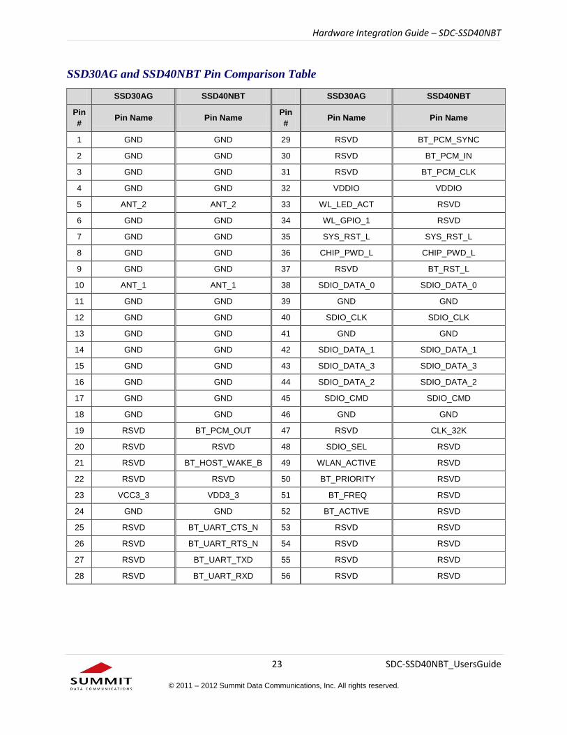
SSD30AG and SSD40NBT Pin Comparison Table
SSD30AG SSD40NBT SSD30AG SSD40NBT
Pin
# Pin Name Pin Name
Pin
# Pin Name Pin Name
1 GND GND 29 RSVD BT_PCM_SYNC
2 GND GND 30 RSVD BT_PCM_IN
3 GND GND 31 RSVD BT_PCM_CLK
4 GND GND 32 VDDIO VDDIO
5 ANT_2 ANT_2 33 WL_LED_ACT RSVD
6 GND GND 34 WL_GPIO_1 RSVD
7 GND GND 35 SYS_RST_L SYS_RST_L
8 GND GND 36 CHIP_PWD_L CHIP_PWD_L
9 GND GND 37 RSVD BT_RST_L
10 ANT_1 ANT_1 38 SDIO_DATA_0 SDIO_DATA_0
11 GND GND 39 GND GND
12 GND GND 40 SDIO_CLK SDIO_CLK
13 GND GND 41 GND GND
14 GND GND 42 SDIO_DATA_1 SDIO_DATA_1
15 GND GND 43 SDIO_DATA_3 SDIO_DATA_3
16 GND GND 44 SDIO_DATA_2 SDIO_DATA_2
17 GND GND 45 SDIO_CMD SDIO_CMD
18 GND GND 46 GND GND
19 RSVD BT_PCM_OUT 47 RSVD CLK_32K
20 RSVD RSVD 48 SDIO_SEL RSVD
21 RSVD BT_HOST_WAKE_B 49 WLAN_ACTIVE RSVD
22 RSVD RSVD 50 BT_PRIORITY RSVD
23 VCC3_3 VDD3_3 51 BT_FREQ RSVD
24 GND GND 52 BT_ACTIVE RSVD
25 RSVD BT_UART_CTS_N 53 RSVD RSVD
26 RSVD BT_UART_RTS_N 54 RSVD RSVD
27 RSVD BT_UART_TXD 55 RSVD RSVD
28 RSVD BT_UART_RXD 56 RSVD RSVD
Page 24
Hardware Integration Guide – SDC-SSD40NBT
24 SDC-SSD40NBT_UsersGuide
© 2011 – 2012 Summit Data Communications, Inc. All rights reserved.
Electrical Considerations
Below is a section of the schematic for the MSD40NBT, a PCB module based on the SSD40NBT. Summit
provides this for your reference only to aid you in integrating the SSD40NBT into your device.
Note: The full MSD40NBT schematic is located in Appendix A: Schematic.
Figure 3: Recommended circuit for SYS_RST_L
Note: In the reset circuit, the diode is placed in parallel with the resistor to ensure the capacitor is
discharged quickly when a power drop occurs. This minimizes the chance of register corruption
within the processor and Wi-Fi module should such a power supply glitch arise.
Figure 4: Recommended supply bypass
Note: The 10uF bypass capacitors must be a low-ESR type.
Note: The 0 ohm resistors are optional and could be replaced by a chip ferrite bead, if desired.
VCC 3.3V
VCC 3.3V
Page 25
Hardware Integration Guide – SDC-SSD40NBT
25 SDC-SSD40NBT_UsersGuide
© 2011 – 2012 Summit Data Communications, Inc. All rights reserved.
Integration Considerations
The following Wi-Fi and Bluetooth information should be taken into consideration when integrating the
SSD40NBT.
Wi-Fi
Series resistors are recommended in all six SDIO lines (27-56 ohms typically):
SDIO_CLK
SDIO_CMD
SDIO_DATA_0
SDIO_DATA_1
SDIO_DATA_2
SDIO_DATA_3
Note: Although these values may vary with the properties of your host interface and the PCB, they are a
reasonable starting point.
Note: The series resistors in the SDIO bus provide several design benefits:
- If a host controller has too high of a drive strength, then bus ringing may result. Series resistors
can reduce this ringing on the I/O lines.
- Adding 27-56 ohms of series resistance on the SDIO bus will reduce sharp transitional edges,
which may reduce EMI.
- Having the series resistors in the PCB layout allows for design flexibility; If they are later found to
be unnecessary, zero (0) ohm jumpers may be used in their place
The following are also recommended:
47 K ohm pull-ups on the CMD line and four data lines: SDIO_CMD, SDIO_DATA_0, SDIO_DATA_1,
SDIO_DATA_2, SDIO_DATA_3
Note: No pull-up is required on the CLK line.
Note: Make sure to apply the proper voltage on the VDDIO input to the SiP to match the signaling
voltage of the SDIO host interface (1.8V or 3.3V typically, but it can be anything in between these
values).
Note: The SDIO host must wait a minimum of 110 ms before initiating access to the SDC-SSD40NBT
after VDD ramps up and settles.
Page 26
Hardware Integration Guide – SDC-SSD40NBT
26 SDC-SSD40NBT_UsersGuide
© 2011 – 2012 Summit Data Communications, Inc. All rights reserved.
Bluetooth
When the BT radio is not being used, the BT_RST_L line may be held low to save some overall current
consumption.
When the BT radio is being used, the BT_RST_L line may be left floating (because there is a 10 K ohm
pull-up resistor on this line inside the SSD40NBT SiP).
If the BT_RST_L is coming from a GPIO from the host processor, then it may be easier (although not
necessary) to assert a HIGH on this line, rather than making it an input.
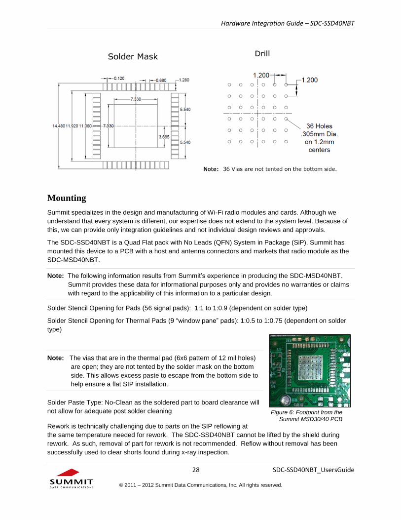
Mechanical Specifications
Page 27
Hardware Integration Guide – SDC-SSD40NBT
27 SDC-SSD40NBT_UsersGuide
© 2011 – 2012 Summit Data Communications, Inc. All rights reserved.
Figure 5: SiP Photo (Bottom View)
Note: The ground pad beneath the SiP (radio) should
be the ground plane of your circuit board. The
exposed portion of the ground pad beneath
the SiP is controlled by the Solder Mask layer.
Page 28
Hardware Integration Guide – SDC-SSD40NBT
28 SDC-SSD40NBT_UsersGuide
© 2011 – 2012 Summit Data Communications, Inc. All rights reserved.
Mounting
Summit specializes in the design and manufacturing of Wi-Fi radio modules and cards. Although we
understand that every system is different, our expertise does not extend to the system level. Because of
this, we can provide only integration guidelines and not individual design reviews and approvals.
The SDC-SSD40NBT is a Quad Flat pack with No Leads (QFN) System in Package (SiP). Summit has
mounted this device to a PCB with a host and antenna connectors and markets that radio module as the
SDC-MSD40NBT.
Note: The following information results from Summit’s experience in producing the SDC-MSD40NBT.
Summit provides these data for informational purposes only and provides no warranties or claims
with regard to the applicability of this information to a particular design.
Solder Stencil Opening for Pads (56 signal pads): 1:1 to 1:0.9 (dependent on solder type)
Solder Stencil Opening for Thermal Pads (9 “window pane” pads): 1:0.5 to 1:0.75 (dependent on solder
type)
Note: The vias that are in the thermal pad (6x6 pattern of 12 mil holes)
are open; they are not tented by the solder mask on the bottom
side. This allows excess paste to escape from the bottom side to
help ensure a flat SIP installation.
Solder Paste Type: No-Clean as the soldered part to board clearance will
not allow for adequate post solder cleaning Rework is technically challenging due to parts on the SIP reflowing at
the same temperature needed for rework. The SDC-SSD40NBT cannot be lifted by the shield during
rework. As such, removal of part for rework is not recommended. Reflow without removal has been
successfully used to clear shorts found during x-ray inspection.
Figure 6: Footprint from the Summit MSD30/40 PCB
Page 29
Hardware Integration Guide – SDC-SSD40NBT
29 SDC-SSD40NBT_UsersGuide
© 2011 – 2012 Summit Data Communications, Inc. All rights reserved.
Reflow: The SDC-SSD40NBT is RoHS compliant and as such is sensitive to heat. The below graphic
details a typical profile for such and device and is provided for reference purposes.
Recommendations:
If the SSD30NBT has been removed from the moisture-protective packaging for more than 24 hours,
bake at 125 degrees Celsius for 24 hours (per Jedec-STD-033). This is a preparatory step prior to reflow
to ensure that the SIPs are sufficiently dehydrated. Reflow should occur immediately following baking to
prevent rehydration.
RF Layout Design Guidelines
The following is a list of RF layout design guidelines and recommendation when installing a Summit radio
into your device.
Do not run antenna cables directly above or directly below the radio.
Do not place any parts or run any high speed digital lines below the radio.
If there are other radios or transmitters located on the device (such as a Bluetooth radio), place the
devices as far apart from each other as possible.
Ensure that there is the maximum allowable spacing separating the antenna connectors on the
Summit radio from the antenna. In addition, do not place antennas directly above or directly below the
radio.
Summit recommends the use of a double shielded cable for the connection between the radio and the
antenna elements.
Use proper electro-static-discharge (ESD) procedures when installing the Summit radio module.
Page 30
Hardware Integration Guide – SDC-SSD40NBT
30 SDC-SSD40NBT_UsersGuide
© 2011 – 2012 Summit Data Communications, Inc. All rights reserved.
Regulatory
Certified Antennas
The SDC-SSD40NBT will be tested to the regulatory standards defined in the “Certifications” section of
the Specifications table above. Summit plans to conduct these tests with the following antennas:
Cisco AIR-ANT 4941
Form Factor: Whip
Type: Dipole
Maximum 2.4 GHz Gain: 2.2 dBi
Tested and Certified 2.4 GHz Transmit Power: TBD
Ethertronics
Form Factor: Isolated Magnetic Dipole™ (IMD)
Type: GY Internal Antenna
Maximum 2.4 GHz Gain: 2.5 dBi
Maximum 5 GHz Gain: 5 dBi
Tested and Certified 2.4 GHz Transmit Power: TBD
Tested and Certified 5 GHz Transmit Power: TBD
Radiall Larson Dipole (R380500314)
Form Factor: Whip
Type: Dipole
Maximum 2.4 GHz Gain: 1.6 dBi (not used during testing)
Maximum 5 GHz Gain: 5 dBi
Tested and Certified 5 GHz Transmit Power: TBD
HUBER+SUHNER (SOA 2459/360/5/0/V_C)
Form Factor: Whip
Type: Monopole
Maximum 2.4 GHz Gain:3dBi
Maximum 5 GHz Gain:6.5dBi
Tested and Certified 2.4 GHz Transmit Power: TBD
Tested and Certified 5 GHz Transmit Power: TBD
Note: If the formal test reports for the SDC-SSD40NBTshow that transmit power was decreased to less
than 100% on 2.4 GHz edge channels. Summit will make these transmit power reductions in
firmware for the edge channels. Integrators do not need to reduce transmit power on a channel-
by-channel basis to comply with band edge regulations.
Page 31
Hardware Integration Guide – SDC-SSD40NBT
31 SDC-SSD40NBT_UsersGuide
© 2011 – 2012 Summit Data Communications, Inc. All rights reserved.
Antennas of differing types and higher gains may be integrated as well. If necessary, with the Summit
Manufacturing Utility software utility, OEMs may reduce the transmit power of the SDC-SSD40NBT to
account for higher antenna gain. In some cases, OEMs may be able to reduce certification efforts by
using antennas that are of like type and equal or lesser gain to the above listed antennas.
Documentation Requirements
In order to maintain regulatory compliance, when integrating the SDC-SSD40NBT into a host device and
leveraging Summit’s grants and certifications, it is necessary to meet the documentation requirements set
forth by the applicable regulatory agencies. The following sections (FCC, Industry Canada, and European
Union) outline the information that may be included in the user’s guide and external labels for the host
devices into which the SDC-SSD40NBT is integrated.
FCC
Note: You must place “Contains FCC ID: TWG-SDCSSD40NBT” on the host product in such a location
that it can be seen by an operator at the time of purchase.
User’s Guide Requirements
When integrating the SDC-SSD40NBT into a host device, the integrator must include specific information
in the user’s guide for the device into which the SDC-SSD40NBT is integrated. The integrator must not
provide information to the end user regarding how to install or remove this RF module in the user’s
manual of the device into which the SDC-SSD40NBT is integrated. The following FCC statements must
be added in their entirety and without modification into a prominent place in the user’s guide for the
device into which the SDC-SSD40NBT is integrated:
Federal Communication Commission Interference Statement
This equipment has been tested and found to comply with the limits for a Class B digital device,
pursuant to Part 15 of the FCC Rules. These limits are designed to provide reasonable protection
against harmful interference in a residential installation. This equipment generates, uses, and can
radiate radio frequency energy and, if not installed and used in accordance with the instructions, may
cause harmful interference to radio communications. However, there is no guarantee that interference
will not occur in a particular installation. If this equipment does cause harmful interference to radio or
television reception, which can be determined by turning the equipment off and on, the user is
encouraged to try to correct the interference by one of the following measures:
1. Reorient or relocate the receiving antenna.
2. Increase the separation between the equipment and receiver.
3. Connect the equipment into an outlet on a circuit different from that to which the receiver is connected.
4. Consult the dealer or an experienced radio/TV technician for help.
Page 32
Hardware Integration Guide – SDC-SSD40NBT
32 SDC-SSD40NBT_UsersGuide
© 2011 – 2012 Summit Data Communications, Inc. All rights reserved.
FCC Caution: Any changes or modifications not expressly approved by the party responsible for
compliance could void the user's authority to operate this equipment.
This device complies with Part 15 of the FCC Rules. Operation is subject to the following two
conditions: (1) This device may not cause harmful interference, and (2) this device must accept any
interference received, including interference that may cause undesired operation.
IMPORTANT NOTE: FCC Radiation Exposure Statement:
This equipment complies with FCC radiation exposure limits set forth for an uncontrolled
environment. This equipment should be installed and operated with minimum distance 20cm between
the radiator & your body.
Industry Canada
Note: You must place “Contains IC ID: 6616A-SDCSSD40NBT” on the host product in such a location
that it can be seen by an operator at the time of purchase.
User’s Guide Requirements (for Model # SDC-SSD40NBT)
RF Radiation Hazard Warning
To ensure compliance with FCC and Industry Canada RF exposure requirements, this device must be
installed in a location where the antennas of the device will have a minimum distance of at least 20 cm
from all persons. Using higher gain antennas and types of antennas not certified for use with this product
is not allowed. The device shall not be co-located with another transmitter.
Installez l'appareil en veillant à conserver une distance d'au moins 20 cm entre les éléments rayonnants
et les personnes. Cet avertissement de sécurité est conforme aux limites d'exposition définies par la
norme CNR-102 at relative aux fréquences radio.
Maximum Antenna Gain – If the integrator configures the device such that the antenna is
detectable from the host product.
This radio transmitter (IC ID: 6616A-SDCSSD40L) has been approved by Industry Canada to operate
with the antenna types listed below with the maximum permissible gain and required antenna impedance
for each antenna type indicated. Antenna types not included in this list, having a gain greater than the
maximum gain indicated for that type, are strictly prohibited for use with this device.
Le présent émetteur radio (IC ID: 6616A-SDCSSD40L) a été approuvé par Industrie Canada pour
fonctionner avec les types d'antenne énumérés ci-dessous et ayant un gain admissible maximal et
l'impédance requise pour chaque type d'antenne. Les types d'antenne non inclus dans cette liste, ou dont
le gain est supérieur au gain maximal indiqué, sont strictement interdits pour l'exploitation de l'émetteur.
Under Industry Canada regulations, this radio transmitter may only operate using an antenna of a type
and maximum (or lesser) gain approved for the transmitter by Industry Canada. To reduce potential radio
Page 33
Hardware Integration Guide – SDC-SSD40NBT
33 SDC-SSD40NBT_UsersGuide
© 2011 – 2012 Summit Data Communications, Inc. All rights reserved.
interference to other users, the antenna type and its gain should be so chosen that the equivalent
isotropically radiated power (e.i.r.p.) is not more than that necessary for successful communication.
Conformément à la réglementation d'Industrie Canada, le présent émetteur radio peut fonctionner avec
une antenne d'un type et d'un gain maximal (ou inférieur) approuvé pour l'émetteur par Industrie Canada.
Dans le but de réduire les risques de brouillage radioélectrique à l'intention des autres utilisateurs, il faut
choisir le type d'antenne et son gain de sorte que la puissance isotrope rayonnée équivalente (p.i.r.e.) ne
dépasse pas l'intensité nécessaire à l'établissement d'une communication satisfaisante.
This device complies with Industry Canada license-exempt RSS standard(s). Operation is subject to the following two conditions: (1) this device may not cause interference, and (2) this device must accept any interference, including interference that may cause undesired operation of the device. Le présent appareil est conforme aux CNR d'Industrie Canada applicables aux appareils radio exempts
de licence. L'exploitation est autorisée aux deux conditions suivantes : (1) l'appareil ne doit pas produire
de brouillage, et (2) l'utilisateur de l'appareil doit accepter tout brouillage radioélectrique subi, même si le
brouillage est susceptible d'en compromettre le fonctionnement.
European Union
User’s Guide Requirements
The integrator must include specific information in the user’s guide for the device into which the SDC-
SSD40NBT is integrated. In addition to the required FCC and IC statements outlined above, the following
R&TTE statements must be added in their entirety and without modification into a prominent place in the
user’s guide for the device into which the SDC-SSD40NBT is integrated:
This device complies with the essential requirements of the R&TTE Directive 1999/5/EC. The
following test methods have been applied in order to prove presumption of conformity with the
essential requirements of the R&TTE Directive 1999/5/EC:
EN60950-1:2001 A11:2004
Safety of Information Technology Equipment
EN 300 328 V1.7.1: (2006-10)
Electromagnetic compatibility and Radio spectrum Matters (ERM); Wideband Transmission
systems; Data transmission equipment operating in the 2,4 GHz ISM band and using spread
spectrum modulation techniques; Harmonized EN covering essential requirements under article
3.2 of the R&TTE Directive
EN 300 328 v1.7.1 (BT 2.1)
EN 301 489-1 V1.6.1: (2005-09)
Electromagnetic compatibility and Radio Spectrum Matters (ERM); ElectroMagnetic Compatibility
(EMC) standard for radio equipment and services; Part 1: Common technical requirements
EN 301 489-17 V1.2.1 (2002-08)
Electromagnetic compatibility and Radio spectrum Matters (ERM); ElectroMagnetic Compatibility
(EMC) standard for radio equipment and services; Part 17: Specific conditions for 2,4 GHz
wideband transmission systems and 5 GHz high performance RLAN equipment
Page 34
Hardware Integration Guide – SDC-SSD40NBT
34 SDC-SSD40NBT_UsersGuide
© 2011 – 2012 Summit Data Communications, Inc. All rights reserved.
EN 301 893
Electromagnetic compatibility and Radio spectrum Matters (ERM); Broadband Radio Access
Networks (BRAN); Specific conditions for 5 GHz high performance RLAN equipment
EU 2002/95/EC (RoHS)
Declaration of Compliance – EU Directive 2003/95/EC; Reduction of Hazardous Substances
(RoHS)
This device is a 2.4 GHz wideband transmission system (transceiver), intended for use in all EU
member states and EFTA countries, except in France and Italy where restrictive use applies.
In Italy the end-user should apply for a license at the national spectrum authorities in order to obtain
authorization to use the device for setting up outdoor radio links and/or for supplying public access to
telecommunications and/or network services.
This device may not be used for setting up outdoor radio links in France and in some areas the RF
output power may be limited to 10 mW EIRP in the frequency range of 2454 – 2483.5 MHz. For
detailed information the end-user should contact the national spectrum authority in France.
Česky
[Czech]
[Jméno výrobce] tímto prohlašuje, že tento [typ zařízení] je ve shodě se
základními požadavky a dalšími příslušnými ustanoveními směrnice
1999/5/ES.
Dansk
[Danish]
Undertegnede [fabrikantens navn] erklærer herved, at følgende udstyr
[udstyrets typebetegnelse] overholder de væsentlige krav og øvrige relevante
krav i direktiv 1999/5/EF.
Deutsch
[German]
Hiermit erklärt [Name des Herstellers], dass sich das Gerät [Gerätetyp] in
Übereinstimmung mit den grundlegenden Anforderungen und den übrigen
einschlägigen Bestimmungen der Richtlinie 1999/5/EG befindet.
Eesti
[Estonian]
Käesolevaga kinnitab [tootja nimi = name of manufacturer] seadme [seadme
tüüp = type of equipment] vastavust direktiivi 1999/5/EÜ põhinõuetele ja
nimetatud direktiivist tulenevatele teistele asjakohastele sätetele.
English Hereby, [name of manufacturer], declares that this [type of equipment] is in
compliance with the essential requirements and other relevant provisions of
Directive 1999/5/EC.
Español
[Spanish]
Por medio de la presente [nombre del fabricante] declara que el [clase de
equipo] cumple con los requisitos esenciales y cualesquiera otras
disposiciones aplicables o exigibles de la Directiva 1999/5/CE.
Ελληνική
[Greek]
ΜΕ ΤΗΝ ΠΑΡΟΥΣΑ [name of manufacturer] ΔΗΛΩΝΕΙ ΟΤΙ [type of
equipment] ΣΥΜΜΟΡΦΩΝΕΤΑΙ ΠΡΟΣ ΤΙΣ ΟΥΣΙΩΔΕΙΣ ΑΠΑΙΤΗΣΕΙΣ ΚΑΙ ΤΙΣ
ΛΟΙΠΕΣ ΣΧΕΤΙΚΕΣ ΔΙΑΤΑΞΕΙΣ ΤΗΣ ΟΔΗΓΙΑΣ 1999/5/ΕΚ.
Français
[French]
Par la présente [nom du fabricant] déclare que l'appareil [type d'appareil] est
conforme aux exigences essentielles et aux autres dispositions pertinentes de
Page 35
Hardware Integration Guide – SDC-SSD40NBT
35 SDC-SSD40NBT_UsersGuide
© 2011 – 2012 Summit Data Communications, Inc. All rights reserved.
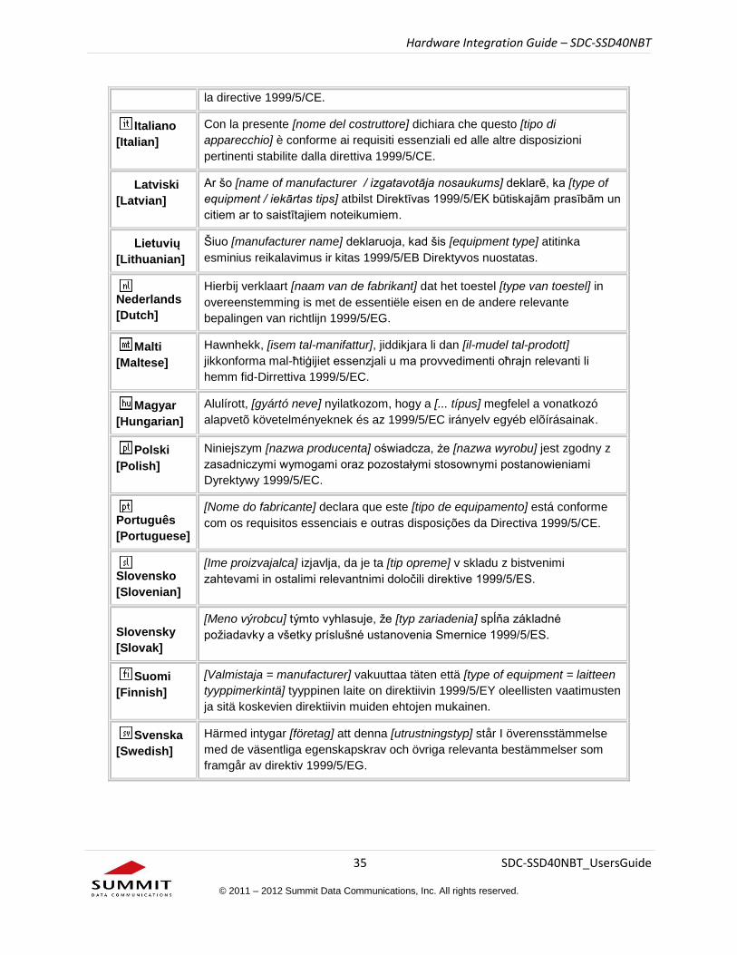
la directive 1999/5/CE.
Italiano
[Italian]
Con la presente [nome del costruttore] dichiara che questo [tipo di
apparecchio] è conforme ai requisiti essenziali ed alle altre disposizioni
pertinenti stabilite dalla direttiva 1999/5/CE.
Latviski
[Latvian]
Ar šo [name of manufacturer / izgatavotāja nosaukums] deklarē, ka [type of
equipment / iekārtas tips] atbilst Direktīvas 1999/5/EK būtiskajām prasībām un
citiem ar to saistītajiem noteikumiem.
Lietuvių
[Lithuanian]
Šiuo [manufacturer name] deklaruoja, kad šis [equipment type] atitinka
esminius reikalavimus ir kitas 1999/5/EB Direktyvos nuostatas.
Nederlands
[Dutch]
Hierbij verklaart [naam van de fabrikant] dat het toestel [type van toestel] in
overeenstemming is met de essentiële eisen en de andere relevante
bepalingen van richtlijn 1999/5/EG.
Malti
[Maltese]
Hawnhekk, [isem tal-manifattur], jiddikjara li dan [il-mudel tal-prodott]
jikkonforma mal-ħtiġijiet essenzjali u ma provvedimenti oħrajn relevanti li
hemm fid-Dirrettiva 1999/5/EC.
Magyar
[Hungarian]
Alulírott, [gyártó neve] nyilatkozom, hogy a [... típus] megfelel a vonatkozó
alapvetõ követelményeknek és az 1999/5/EC irányelv egyéb elõírásainak.
Polski
[Polish]
Niniejszym [nazwa producenta] oświadcza, że [nazwa wyrobu] jest zgodny z
zasadniczymi wymogami oraz pozostałymi stosownymi postanowieniami
Dyrektywy 1999/5/EC.
Português
[Portuguese]
[Nome do fabricante] declara que este [tipo de equipamento] está conforme
com os requisitos essenciais e outras disposições da Directiva 1999/5/CE.
Slovensko
[Slovenian]
[Ime proizvajalca] izjavlja, da je ta [tip opreme] v skladu z bistvenimi
zahtevami in ostalimi relevantnimi določili direktive 1999/5/ES.
Slovensky
[Slovak]
[Meno výrobcu] týmto vyhlasuje, že [typ zariadenia] spĺňa základné
požiadavky a všetky príslušné ustanovenia Smernice 1999/5/ES.
Suomi
[Finnish]
[Valmistaja = manufacturer] vakuuttaa täten että [type of equipment = laitteen
tyyppimerkintä] tyyppinen laite on direktiivin 1999/5/EY oleellisten vaatimusten
ja sitä koskevien direktiivin muiden ehtojen mukainen.
Svenska
[Swedish]
Härmed intygar [företag] att denna [utrustningstyp] står I överensstämmelse
med de väsentliga egenskapskrav och övriga relevanta bestämmelser som
framgår av direktiv 1999/5/EG.
Page 36
Hardware Integration Guide – SDC-SSD40NBT
36 SDC-SSD40NBT_UsersGuide
© 2011 – 2012 Summit Data Communications, Inc. All rights reserved.
Labeling Requirements
The final end product must be labeled in a visible area with the following notice:


![SDC-12/SDC-15 · 2018-01-14 · Introduction 6 SDC-12/SDC-151080pD-ILA3D Front Projector2013 User’s Manual AdditionalOptionalAccessories Replacementlamps: •FormodelsSDC-12andSDC-15[2013productionandbeyond]orderlampWC-LPU230](https://static.documents.pub/doc/80x56/5f30eb9530d2254a2869f490/sdc-12sdc-15-2018-01-14-introduction-6-sdc-12sdc-151080pd-ila3d-front-projector2013.jpg)


