8.4. Disassembly Procedures of Camera Lens Unit 33
9 Measurements and Adjustments 34 9.1. EEPROM Data for spare parts of the SUB P.C.B. 34
(K)........Black Type (except DMR-H80GK)(S)........Silver Type (except DMR-H80EF, H81, H90)(A)........Blue Type (except DMR-H80EF/EE, H81, H90)(R)........Red Type (except DMR-H80EE, H81, H90)
9.2. Service Positions 34
9.3. Location for Connectors of the Main P.C.B. and Sub
P.C.B. 36
9.4. Electrical Adjustment Procedures 38
10 Maintenance 42 10.1. Cleaning Lens and LCD Panel 42
1. Plug the AC cord directly into the AC outlet. Do not use anisolation transformer for this check.
2. Connect “A” to exposed metallic part on the set. Andconnect “B” to a good earth ground, as shown in .
3. Use an AC voltmeter, with 1 k�/V or more sensitivity, tomeasure the potential across the resistor.
4. Check each exposed metallic part, and measure thevoltage at each point.
5. Reverse the AC plug in the AC outlet and repeat each of theabove measurements.
6. The potential at any point should not exceed 0.25 V RMS.A leakage current tester (Simpson Model 229 or equivalent)may be used to make the hot checks, leakage current mustnot exceed 1/2 mA. In case a measurement is outside ofthe limits specified, there is a possibility of a shock hazard,and the equipment should be repaired and recheckedbefore it is returned to the customer.
Figure 1
1 Safety Precaution1.1. General Guidelines 1. IMPORTANT SAFETY NOTICE
There are special components used in this equipment which are important for safety. These parts are marked by in theSchematic Diagrams, Circuit Board Layout, Exploded Views and Replacement Parts List. It is essential that these critical partsshould be replaced with manufacturer’s specified parts to prevent X-RADIATION, shock fire, or other hazards. Do not modifythe original design without permission of manufacturer.
2. An Isolation Transformer should always be used during the servicing of AC Adaptor whose chassis is not isolated from the ACpower line. Use a transformer of adequate power rating as this protects the technician from accidents resulting in personal injuryfrom electrical shocks. It will also protect AC Adaptor from being damaged by accidental shorting that may occur duringservicing.
3. When servicing, observe the original lead dress. It a short circuit is found, replace all parts which have been overheated ordamaged by the short circuit.
4. After servicing, see to it that all the protective devices such as insulation barriers, insulation papers shields are properlyinstalled.
5. After servicing, make the following leakage current checks to prevent the customer from being exposed to shock hazards.
1.1.1. Leakage Current Cold Check 1. Unplug the AC cord and connect a jumper between the two prongs on the plug. 2. Measure the resistance value, with an ohmmeter, between the jumpered AC plug and each exposed metallic cabinet part on
the equipment such as screwheads, connectors, control shafts, etc. When the exposed metallic part has a return path to thechassis, the reading should be between 1M� and 5.2M�. When the exposed metal does not have a return path to the chassis,the reading must be infinity.
1.1.2. Leakage current hot check (See Figure 1)
3
SDR-H80P
2 Warning2.1. Prevention of Electrostatic Discharge (ESD) to Electrostatic Sensitive
(ES) DevicesSome semiconductor (solid state) devices can be damaged easily by static electricity. Such components commonly are calledElectrostatic Sensitive (ES) Devices. Examples of typical ES devices are integrated circuits and some field-effect transistors andsemiconductor “chip” components. The following techniques should be used to help reduce the incidence of component damagecaused by electrostatic discharge (ESD).
1. Immediately before handling any semiconductor component or semiconductor-equipped assembly, drain off any ESD on yourbody by touching a known earth ground. Alternatively, obtain and wear a commercially available discharging ESD wrist strap,which should be removed for potential shock reasons prior to applying power to the unit under test.
2. After removing an electrical assembly equipped with ES devices, place the assembly on a conductive surface such asaluminum foil, to prevent electrostatic charge buildup or exposure of the assembly.
3. Use only a grounded-tip soldering iron to solder or unsolder ES devices. 4. Use only an antistatic solder removal device. Some solder removal devices not classified as “antistatic (ESD protected)” can
generate electrical charge sufficient to damage ES devices. 5. Do not use freon-propelled chemicals. These can generate electrical charges sufficient to damage ES devices. 6. Do not remove a replacement ES device from its protective package until immediately before you are ready to install it. (Most
replacement ES devices are packaged with leads electrically shorted together by conductive foam, aluminum foil or comparableconductive material).
7. Immediately before removing the protective material from the leads of a replacement ES device, touch the protective materialto the chassis or circuit assembly into which the device will be installed.CAUTION:
Be sure no power is applied to the chassis or circuit, and observe all other safety precautions. 8. Minimize bodily motions when handling unpackaged replacement ES devices. (Otherwise harmless motion such as the
brushing together of your clothes fabric or the lifting of your foot from a carpeted floor can generate static electricity (ESD)sufficient to damage an ES device).
4
SDR-H80P
2.2. Service caution based on legal restrictions2.2.1. General description about Lead Free Solder (PbF)The lead free solder has been used in the mounting process of all electrical components on the printed circuit boards used for thisequipment in considering the globally environmental conservation.
The normal solder is the alloy of tin (Sn) and lead (Pb). On the other hand, the lead free solder is the alloy mainly consists of tin(Sn), silver (Ag) and Copper (Cu), and the melting point of the lead free solder is higher approx.30 degrees C (86°F) more than thatof the normal solder.
Definition of PCB Lead Free Solder being usedThe letter of “PbF” is printed either foil side or components side on the PCB using the lead free solder.(See right figure)
Service caution for repair work using Lead Free Solder (PbF)���� ·����The lead free solder has to be used when repairing the equipment for which the lead free solder is used.
(Definition: The letter of “PbF” is printed on the PCB using the lead free solder.)���� ·����To put lead free solder, it should be well molten and mixed with the original lead free solder.���� ·����Remove the remaining lead free solder on the PCB cleanly for soldering of the new IC.���� ·����Since the melting point of the lead free solder is higher than that of the normal lead solder, it takes the longer time to melt
the lead free solder.���� ·����Use the soldering iron (more than 70W) equipped with the temperature control after setting the temperature at 350±30
degrees C (662±86°F).Recommended Lead Free Solder (Service Parts Route.)
���� ·����The following 3 types of lead free solder are available through the service parts route.RFKZ03D01KS-----------(0.3mm 100g Reel)RFKZ06D01KS-----------(0.6mm 100g Reel)RFKZ10D01KS-----------(1.0mm 100g Reel)
Note* Ingredient: tin (Sn), 96.5%, silver (Ag) 3.0%, Copper (Cu) 0.5%, Cobalt (Co) / Germanium (Ge) 0.1 to 0.3%
5
SDR-H80P
2.3. Caution for AC Cord(For EB/GC)
2.3.1. Information for your safetyIMPORTANT
Your attention is drawn to the fact that recording of pre-recorded tapes or discs or other published or broadcastmaterial may infringe copyright laws.
WARNINGTo reduce the risk of fire or shock hazard, do not exposethis equipment to rain or moisture.
CAUTIONTo reduce the risk of fire or shock hazard and annoyinginterference, use the recommended accessories only.
FOR YOUR SAFETYDO NOT REMOVE THE OUTER COVERTo prevent electric shock, do not remove the cover. No userserviceable parts inside. Refer servicing to qualified servicepersonnel.
2.3.2. Caution for AC mains leadFor your safety, please read the following text carefully.
This appliance is supplied with a moulded three-pin mains plugfor your safety and convenience.A 5-ampere fuse is fitted in this plug.Should the fuse need to be replaced please ensure that thereplacement fuse has a rating of 5 amperes and it is approvedby ASTA or BSI to BS1362Check for the ASRA mark or the BSI mark on the body of thefuse.
If the plug contains a removable fuse cover you must ensurethat it is refitted when the fuse is replaced.If you lose the fuse cover, the plug must not be used until areplacement cover is obtained.A replacement fuse cover can be purchased from your localPanasonic Dealer.
If the fitted moulded plug is unsuitable for the socket outlet inyour home then the fuse should be removed and the plug cutoff and disposed of safety.There is a danger of severe electrical shock if the cut off plugis inserted into any 13-ampere socket.
If a new plug is to be fitted please observe the wiring code asshown below.If in any doubt, please consult a qualified electrician.
2.3.2.1. ImportantThe wires in this mains lead are coloured in accordance withthe following code:
Blue NeutralBrown Live
As the colours of the wires in the mains lead of this appliancemay not correspond with the coloured markings identifying theterminals in your plug, proceed as follows:
The wire which is coloured BLUE must be connected to theterminal in the plug which is marked with the letter N orcoloured BLACK.
The wire which is coloured BROWN must be connected to theterminal in the plug which is marked with the letter L or colouredRED.
Under no circumstances should either of these wires beconnected to the earth terminal of the three pin plug, markedwith the letter E or the Earth Symbol.
2.3.2.2. Before useremove the Connector Cover as follows.
2.3.2.3. How to replace the Fuse 1. Remove the Fuse Cover with a screwdriver.
2. Replace the fuse and attach the Fuse cover.
6
SDR-H80P
2.4. How to Replace the Lithium Battery (PROCEDURE) 1. Remove the LCD BL P.C.B.. (Refer to Disassembly Procedures.) 2. Remove the Lithium Battery “ML-614S/ZTE” and then replace the new one. (See .)
Fig. B1
Note:The lithium battery is a critical component. (Type No.: ML-614S/ZTE Manufactured by Panasonic.)It must never be subjected to excessive heat or discharge.It must therefore only be fitted in equipment designed specifically for its use.Replacement batteries must be of the same type and manufacture.They must be fitted in the same manner and location as the original battery, with the correct polarity contacts observed.Do not attempt to re-charge the old battery or re-use it for any other purpose.It should be disposed of in waste products destined for burial rather than incineration.
7
SDR-H80P
2.5. How to Recycle the Lithium Battery (U.S. Only)
8
SDR-H80P
3 Service Navigation3.1. Service InformationThis service manual contains technical information which will allow service personnel´s to understand and service this model.Please place orders using the parts list and not the drawing reference numbers.If the circuit is changed or modified, this information will be followed by supplement service manual to be filed with original servicemanual.Notes 1:
1. VSK0697 is indicated on AC Adapter used on the following models:SDR-H80P/PC, H90P/PC.However, the AC Adapter replacement part number is DE-A51BB which should be used when ordering.
2. VSK0698 is indicated on AC Adapter used in the following models:SDR-H80EG/EB/EP/EF/EC/EE/GC/GN/GJ/PU, H81EB/EE, H90EG/EB/EP/EF/EC/EE/GC/GN/GJ/PU.However, the AC Adapter replacement part number is DE-A51CB which should be used when ordering.
3. VSK0699 is indicated on AC Adapter used on the following model:SDR-H80GK, H90GK.However, the AC Adapter replacement part number is DE-A51DB which should be used when ordering.
4. VSK0705 is indicated on AC Adapter used on the following model:SDR-H80PR.However, the AC Adapter replacement part number is DE-A51FB which should be used when ordering.
Notes 2:1) This service manual does not contain the following information, because of the impossibility of servicing at component level.
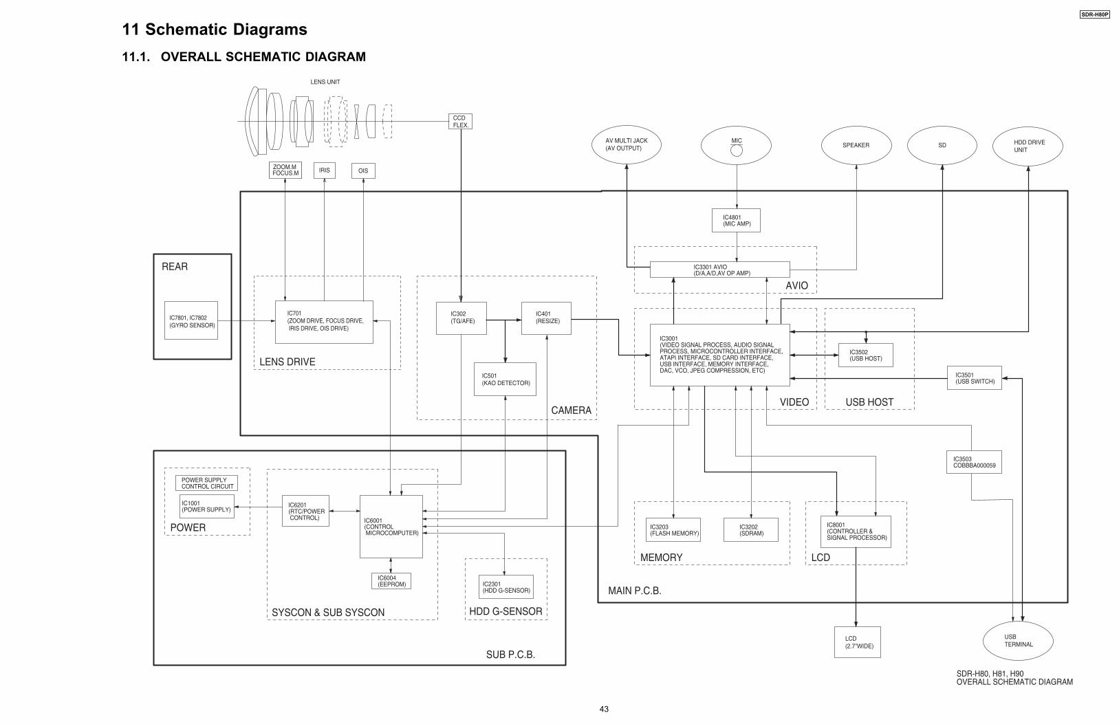
1. Schematic Diagram, Block Diagram and P.C.B. layout of Main P.C.B. and Sub P.C.B.2. Parts List for individual parts of Main P.C.B. and Sub P.C.B.
2) The following category are recycle module part. Please send them to Central Repair Center.*Main P.C.B. (LSEP8462A1: SDR-H80P/PC/PU/PR, H90P/PC/PU)
When a part replacement is required for repairing each Main P.C.B. and Sub P.C.B., replace the assembly parts.(Main P.C.B.)The following circuits are contained in Main P.C.B. 1. Main Connection Circuit 2. AVIO Circuit 3. Video Circuit 4. Memory Circuit 5. USB Host Circuit 6. LCD Circuit 7. Resize Circuit 8. KAO Circuit 9. Lens Drive Circuit 10. TG/AFE Circuit 11. MIC Circuit 12. Sub Power Circuit
9
SDR-H80P
(Sub P.C.B.)The following circuits are contained in Sub P.C.B. 1. Sub Connection Circuit 2. Power Circuit 3. G-Sensor Circuit 4. Sub SYSCON Circuit 5. SYSCON Circuit 6. Light Circuit (Only SDR-H81EE)
10
SDR-H80P
3.2. Precautions for Handling HDD 1. Handle HDD very carefully to prevent the static electricity and shock. 2. Set the HDD quickly after taking it out from the package. Make sure to put the HDD on buffer materials, etc.
3.2.1. Precautions at incoming process and for opening packages
11
SDR-H80P
3.2.2. Precautions for installing HDD
12
SDR-H80P
3.2.3. Precautions for inserting and removing HDD FPCMake sure to use the tool (LSVQ0112) when locking and unlocking the lock lever of HDD FPC connector.Do not lock the lock lever without inserting HDD FPC. Otherwise, the connector may be damaged.
13
SDR-H80P
Make sure to use the tool (LSVQ0112) when opening and closing the lock lever.*See "" () for attaching to the unit.
14
SDR-H80P
3.3. Formatting HDDWhen HDD is exchanged, format HDD as the procedure below.Without formatting, the error message appears on the LCD display when accessing HDD.<Formatting procedure>
Rotate the mode dial to select .Select [HDD] in [MEDIA SELECT]. 1. Press the MENU button, then
select [SETUP] ����
[FORMAT HDD] ���� [YES] andpress the joystick.
2. When the confirmation messageappears, select [YES], then pressthe joystick.
���� ·����When formatting is complete, press the MENUbutton to exit the message screen.Note:
���� ·����During formatting, do not turn this unit off.���� ·����When you format the HDD, use a battery with
sufficient battery power or the AC adaptor.���� ·����During formatting, do not cause any vibrations
or impacts to this unit.
15
SDR-H80P
4 Specifications
16
SDR-H80P
5 Location of Controls and ComponentsFollowings are the Location of Controls and Components for SDR-H80P/PC, H90P/PC as a sample.For other models, refer to each Operating Instructions.
17
SDR-H80P
18
SDR-H80P
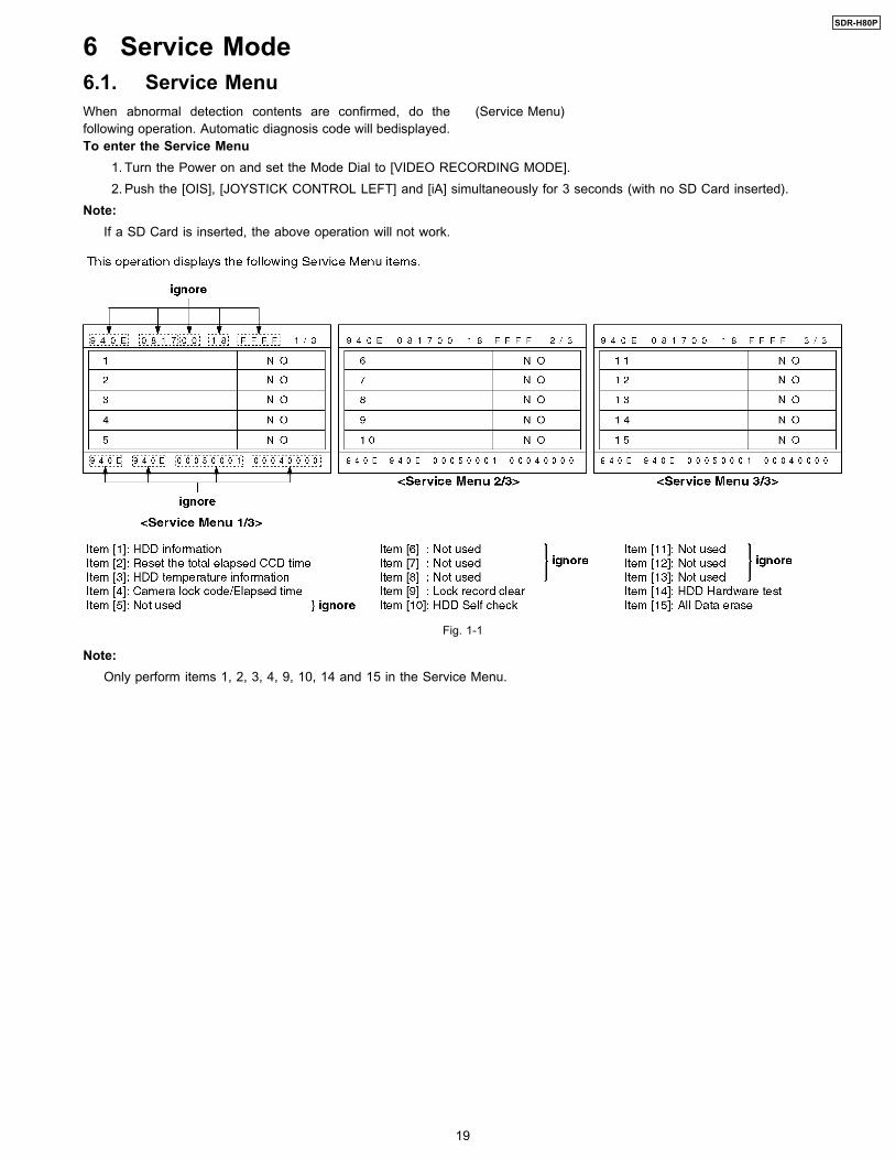
When abnormal detection contents are confirmed, do thefollowing operation. Automatic diagnosis code will bedisplayed.
(Service Menu)
6 Service Mode6.1. Service Menu
To enter the Service Menu 1. Turn the Power on and set the Mode Dial to [VIDEO RECORDING MODE]. 2. Push the [OIS], [JOYSTICK CONTROL LEFT] and [iA] simultaneously for 3 seconds (with no SD Card inserted).
Note:If a SD Card is inserted, the above operation will not work.
Fig. 1-1
Note:Only perform items 1, 2, 3, 4, 9, 10, 14 and 15 in the Service Menu.
19
SDR-H80P
To select the Item of Service Menu 1. Press [JOYSTICK CONTROL UP/DOWN] to select item [1], [2], [3], [4], [9], [10], [14] or [15]. 2. Press [JOYSTICK CONTROL RIGHT] to display [YES/NO] screen. 3. Press [JOYSTICK CONTROL UP/DOWN] to select [YES]. 4. Press [JOYSTICK CONTROL CENTER] to end.
Fig. 1-2
20
SDR-H80P
Fig. 1-3
21
SDR-H80P
Fig. 1-4
22
SDR-H80P
Fig. 1-5
23
SDR-H80P
Fig. 1-6
Fig. 1-7
To exit the Service MenuUnplug the AC Cord.
24
SDR-H80P
6.2. About Default SettingThe data of Menu, Mode, Card and EEPROM setting, etc. is set to the default condition in factory.
6.2.1. How to set the Default Setting 1. Turn the Power on and set the Mode Dial to [VIDEO RECORDING MODE]. 2. When pressing [OIS], [JOYSTICK CONTROL RIGHT] and [iA] for more than 3 minutes simultaneously (with no SD Card
inserted), the items below are set to the Default Setting.
1. Menu, Mode, Adjusted Value2. Card format3. Reset of picture files and directory number (Set the picture record file number to 1)4. Clear the information of Mechanism Lock5. Set the time setting to no-setting
25
SDR-H80P
7 Service Fixture & Tools7.1. Service Tools and Equipment
26
SDR-H80P
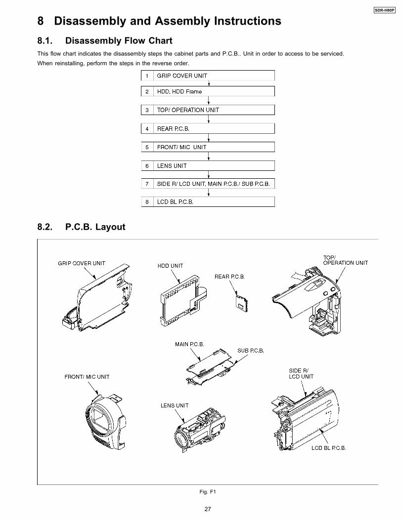
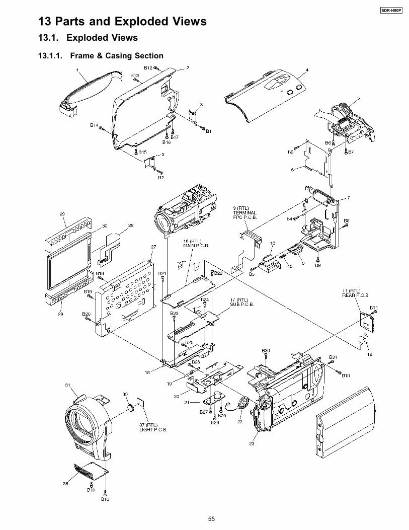
8 Disassembly and Assembly Instructions8.1. Disassembly Flow ChartThis flow chart indicates the disassembly steps the cabinet parts and P.C.B.. Unit in order to access to be serviced.When reinstalling, perform the steps in the reverse order.
8.2. P.C.B. Layout
Fig. F1
27
SDR-H80P
Flow-Chart for Disassembly ProcedureNo. Item / Part Fig. Removal (Screw,Connector,FPC.
& Other)1 5-Screws (A)
1-Screw (B)5-TabsGrip Cover Unit
2 HDD, HDD Frame HDD Damper Unit1-Connector FP21Note for replacing HDD1) How to RemoveHDD CushionHDDNote for replacing HDD2) How to Attach2-Screws (C)1-Screw (D)HDD Frame
3 Top/ OperationUnit
2-Connectors FP11, FP61Open the LCD Unit2-Screws (E)1-Screw (F)Top/ Operation Unit
8 LCD BL P.C.B. Turn the LCD Case to the arrowdirection so that the screws canbe seen, and remove the 2screws (N).8-TabsLCD Case A Unit1-Connector FP8101Side R/ Speaker UnitLCD Case B Unit1-Connector FP81042-Screws (O)Menu selector UnitDeco Piece1-Connector FP81028-TabsLCD BL P.C.B.
Fig. D1
Fig. D2
8.3. Disassembly Procedures
28
SDR-H80P
Fig. D3
Note for replacing HDD���� ·����Be sure to use the tool when inserting and removing
HDD FPC.
After replacing the HDD, be sure to format the new HDD.See “Formatting HDD” in Service Navigation.
1) How to RemoveRemove the HDD cushion from the HDD.Remove the HDD FPC from HDD using the tool.
Fig. D4
2) How to AttachAttach the HDD FPC to the new HDD using the tool.Attach the HDD cushion to the HDD.
Fig. D5
Fig. D6
29
SDR-H80P
Fig. D7
Fig. D8
Fig. D9
Fig. D10
30
SDR-H80P
Fig. D11
Fig. D12
Fig. D13
Fig. D14
31
SDR-H80P
Fig. D15
32
SDR-H80P
8.4. Disassembly Procedures of Camera Lens UnitThe following flowchart describes order or steps for removing the Camera lens unit and certain printed circuit boards in order tomake access to the item needing service.To reassemble the unit follow the steps in reverse order.
Fig. L1
Fig. L2
33
SDR-H80P
9 Measurements and Adjustments9.1. EEPROM Data for spare parts of the SUB P.C.B.After replacing the SUB P.C.B., be sure to achieve adjustment.As for Adjustment condition/procedure, consult the “Adjustment Manual” which is available in Adjustment software.The Adjustment software is available at “TSN Website”, therefore, access to “TSN Website” at “Support Information fromNWBG/VDBG-PAVC”.
9.2. Service Positions
9.2.1. List of the extension cablesUse the following extension cables when checking or adjusting individual circuit boards except module Parts (Main P.C.B. and SubP.C.B.).
34
SDR-H80P
9.2.2. Checking and repairing individual circuit boards except module parts (MainP.C.B. and Sub P.C.B.)
How to use extension cables.
35
SDR-H80P
9.3.1. Main P.C.B.9.3. Location for Connectors of the Main P.C.B. and Sub P.C.B.
36
SDR-H80P
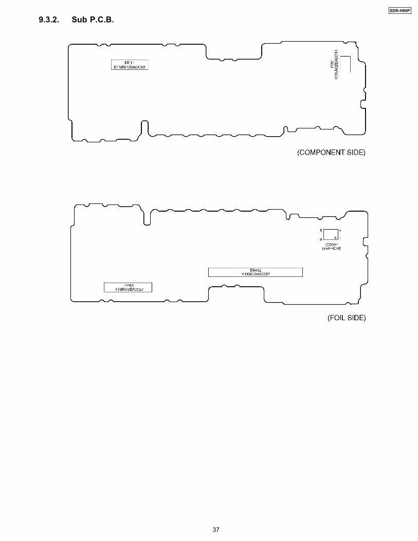
9.3.2. Sub P.C.B.
37
SDR-H80P
9.4. Electrical Adjustment Procedures
9.4.1. Initial GuidelineThe table below shows which adjustments are necessary according to the unit parts and individual parts to be replaced.Make sure to perform these adjustments shown below as necessary.
9.4.2. Set-up manual for SD Card/Hard Disk Video Camera. 1. Installation of USB-SERIAL Driver
Execute the “Setup.exe” file in “Com Mass” folder by double clicking to install the USB-SERIAL driver. 2. Set-Up
a. Remove the SD card from this unit. b. To enter the PC connection (COM) mode, push the [OIS] button, [iA] button and [JOYSTICK CONTROL UP] simultaneously
for 3 seconds without connecting the USB Cable.
38
SDR-H80P
c. Connect the PC and SD Card/Hard Disk Video Camera as shown in and E2.
Fig. E1
Fig. E2 Rough image of set-up connection
39
SDR-H80P
9.4.3. Set up of PC-EVR AdjustmentProgram
1. Turn on the PC and install the PC-EVR AdjustmentProgram into the PC.
2. Execute the "khd2009.exe" file by double clicking to start upthe PC-EVR Adjustment Program.The main menu will be displayed.
3. Select the appropriate model. 4. Turn on the camcorder and set to PC connection (COM)
mode. Then click "Start".Note:
When the camcorder does not power on, turn the poweron with forced power on function.<How to turn the power on with forced power on function>Push and hold the [MENU] and [JOYSTICK CONTROLRIGHT], then set [POWER SW] to ON until the power isturned on.
Fig. E2-1
5. When the communication is complete, the dialog willappear.Click "Yes" and "Save" to save the EEPROM data.
Fig. E2-2
6. When EEPROM data has been saved, the menu willappear.To perform each adjustment, display the adjustment menuby selecting from "Camera Adjust" or "Video Adjust" andselect each adjustment item.
Fig. E2-3
Note:The adjusted data is stored in the EEPROM IC aftereach adjustment.
7. After adjustment, to close the software, select "Exit" in theFile menu or close the window.
Fig. E2-4
8. To release the PC connection (COM) mode, push the [OIS],[iA] and [JOYSTICK CONTROL UP] simultaneously for 3seconds with the USB Cable disconnected.
9.4.4. How to confirm "OneNAND-FlashROM Error"
If there is a problem with Flash ROM (IC3203), the unit doesnot turn the power on.(Problem: When the power SW is turned on, the power LEDlights for 3 seconds and goes out. The power can not be turnedon again.)If this problem occurs, check if the Flash ROM (IC3203) has aproblem in the following procedure.
1. Start PC-EVR Adjustment Program.Refer to "9.4.3. Set up of PC-EVR Adjustment Program"and start PC-EVR Adjustment Program.
40
SDR-H80P
2. Select the "Diagnosis"
Fig. E2-5
3. Select the "Lock Info"
Fig. E2-6
4. Confirm the OneNAND-Flash ROM Error information.
Fig. E2-7
5. If "Fatal Error" is displayed, Flash ROM (IC3203) isdefective. Replace Main P.C.B.Note:
This error information is recorded on EEPROM.Click "Error Reset" to clear the error information afterreplacing Flash ROM (IC3203).
Fig. E2-8
41
SDR-H80P
10 Maintenance10.1. Cleaning Lens and LCD PanelDo not touch the surface of the lens and LCD Panel with your hand.When cleaning the lens, use air-Blower to blow off the dust.When cleaning the LCD Panel, dampen the lens cleaning paper with lens cleaner, and the gently wipe the their surface.Note:
A lens cleaning paper and lens cleaner are available at local camera shops and market place.
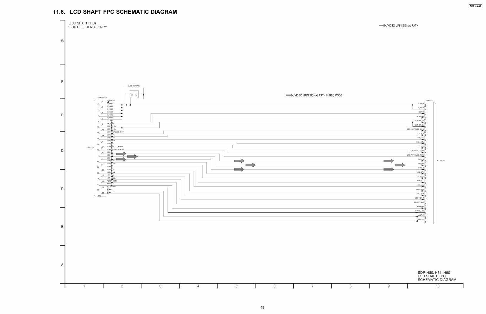
NOTE:DO NOT USE ANY PART NUMBER SHOWN ONTHIS SCHEMATIC DIAGRAM FOR ORDERING.WHEN YOU ORDER A PART, PLEASE REFERTO PARTS LIST.
NOTE:THE MEASUREMENT MODE OF THE DC VOLTAGE ON THIS DIAGRAM IS STOP MODE.
NOTE:CIRCUIT VOLTAGE AND WAVEFORM DESCRIBED HEREIN SHALL BE REGARDED AS REFERENCE INFORMATION WHEN PROBING DEFECT POINT,BECAUSE IT MAY DIFFER FROM AN ACTUAL MEASURING VALUE DUE TO DIFFERENCE OF MEASURINGINSTRUMENT AND ITS MEASURING CONDITION AND PRODUCT ITSELF.
SDR-H80P
46
11.4. LCD BL SCHEMATIC DIAGRAM
NOTE:DO NOT USE ANY PART NUMBER SHOWN ONTHIS SCHEMATIC DIAGRAM FOR ORDERING.WHEN YOU ORDER A PART, PLEASE REFERTO PARTS LIST.
NOTE:THE MEASUREMENT MODE OF THE DC VOLTAGE ON THIS DIAGRAM IS STOP MODE. (LCD: ON)
NOTE:CIRCUIT VOLTAGE AND WAVEFORM DESCRIBED HEREIN SHALL BE REGARDED AS REFERENCE INFORMATION WHEN PROBING DEFECT POINT,BECAUSE IT MAY DIFFER FROM AN ACTUAL MEASURING VALUE DUE TO DIFFERENCE OF MEASURINGINSTRUMENT AND ITS MEASURING CONDITION AND PRODUCT ITSELF.
SDR-H80, H81, H90LCD BL SCHEMATIC DIAGRAM
(LCD BL P.C.B.)
IMPORTANT SAFETY NOTICE:COMPONENTS IDENTIFIED WITH THE MARK HAVE THE SPECIALCHARACTERISTICS FOR SAFETY. WHEN REPLACING ANY OF THESECOMPONENTS, USE ONLY THE SAME TYPE.
E.S.D. standards for Electrostatically Sensitive Devices, referto PREVENTION OF ELECTROSTATIC DISCHARGE (ESD)TO ELECTROSTATICALLY SENSITIVE (ES) DEVICESsection.Definition of Parts supplier:
1. Parts indicated with PSECI in the Remarks column aresupplied by PSECI.
2. All parts except parts indicated with (PSECI) in theRemarks column are supplied by AVC-CSC-SPC.
3. Parts marked with [Energy] in the Remarks column aresupplied from "Panasonic Corporation EnergyCompany."
13.2.1. Frame & Casing Section Parts List
Ref.No.
Part No. Part Name &Description
Pcs Remarks
1 LSGQ0292 GRIP BELT UNIT 12 LSKM1783 GRIP COVER 1 H80EBA/S,ECA/S,
201 LSKM1777-1 LCD CASE B 1 H80EBA/K/R,ECA/K/R,EEK,EFK/R,EGA/K/R,EPA/K/R,GCA/K/R,GJA/K/R,GKA/R,GNA/K/R,PA/K/R,PCA/K/R,PUA/K/R,PRA/K/R,H90EG,EP,GC,GJ,GK,GN,P,PC,PU
201 LSKM1777 LCD CASE B 1 H80EBS,ECS,EES,EGS,EPS,GCS,GJS,GKS,GNS,PS,PCS,PUS,PRS,H81EB,EE,H90EB,EC,EE,EF
202 LSGU0754-1 MENU BUTTON 1 H80EBA/K/R,ECA/K/R,EEK,EFK/R,EGA/K/R,EPA/K/R,GCA/K/R,GJA/K/R,GKA/R,GNA/K/R,PA/K/R,PCA/K/R,PUA/K/R,PRA/K/R,H90EG,EP,GC,GJ,GK,GN,P,PC,PU
202 LSGU0754 MENU BUTTON 1 H80EBS,ECS,EES,EGS,EPS,GCS,GJS,GKS,GNS,PS,PCS,PUS,PRS,H81EB,EE,H90EB,EC,EE,EF
216 LSYK2579 LCD CASE A UNIT 1 (-A) H80216 LSYK2586 LCD CASE A UNIT 1 H80EBK,ECK,EEK,
EFK,EGK,EPK,GCK,GJK,GNK,PK,PCK,PUK,PRK,H81EB
216 LSYK2578 LCD CASE A UNIT 1 (-R) H80216 LSYK2479 LCD CASE A UNIT 1 (-S) H80216 LSYK2740 LCD CASE A UNIT 1 H81EEK [PSECI]216 LSYK2531 LCD CASE A UNIT 1 (-K) H90
401 LSXN0057 LENS UNIT 1401-1 L6HA66NB0011 ZOOM MOTOR UNIT 1401-2 L6HA66NB0012 FOCUS MOTOR UNIT 1401-3 LSEM0114 AUTO IRIS UNIT 1402 LSEP8466A1 CCD P.C.B. 1 (RTL) E.S.D.403 LSDW0141 CCD CASE 1404 LSFL0343 OPTICAL LPF 1405 LSMX0246 CCD CUSHION 1