Sebastian J. Davis, Michal Macha, Andrey Chernev, David M. Huang, Aleksandra Radenovic, and Sanjin Marion Pressure-induced enlargement and ionic current rectification in symmetric nanopores Nano Letters, 2020; 20(11):8089-8095
Pressure Induced Enlargement and Ionic Current Rectification in SymmetricNanopores
Sebastian J. Davis,1 Michal Macha,1 Andrey Chernev,1 David
M. Huang,2 Aleksandra Radenovic,1, ∗ and Sanjin Marion1, ∗
1Laboratory of Nanoscale Biology, Institute of Bioengineering,School of Engineering, EPFL, 1015 Lausanne, Switzerland
2Department of Chemistry, School of Physical Sciences, The University of Adelaide, Adelaide, Australia
Nanopores in solid state membranes are a tool able to probe nanofluidic phenomena, or can act asa single molecular sensor. They also have diverse applications in filtration, desalination, or osmoticpower generation. Many of these applications involve chemical, or hydrostatic pressure differenceswhich act on both the supporting membrane, and the ion transport through the pore. By usingpressure differences between the sides of the membrane, and an alternating current approach toprobe ion transport, we investigate two distinct physical phenomena: the elastic deformation of themembrane through the measurement of strain at the nanopore, and the growth of ionic currentrectification with pressure due to pore entrance effects.
I. INTRODUCTION
Nanopores are a single molecule tool with diverse ap-plications in bio-sensing,1,2 osmotic power generation3
and water desalination.4 A nanoscale pore separates tworeservoirs filled with electrolyte. Monitoring ion trans-port through the pore yields information about a passinganalyte such as DNA, or on non-linear phenomena suchas ionic current rectification (ICR)5 and other nanoflu-idic effects.6–8 Solid state nanopores are readily madein silicon nitride suspended membranes since they arecompatible with standard lithography techniques. Poresin these suspended membranes can be used as such, asin this study, or can further support a membrane madeof quasi-2D materials such as molybdenum disulphide,hexagonal boron nitride, or graphene in which a smallpore can be further drilled.9
The combination of hydrostatic pressure gradientswith nanopores has so far been mostly used to study ana-lyte translocations,10–13 the surface charge of the pore,14
or as a tool to control wetting.15. It has been shown thatpressure can strongly influence the ion transport prop-erties of a nanopore or nanochannel depending on thesystem’s resistance to hydraulic fluid flow, and modu-late ion transport.16,17 On the other hand, ionic currentrectification,7 which is linked to ion selectivity, has beenfound to be reduced in conical pores under the influenceof pressure induced fluid flow.18,19
The application of pressure on thin supported mem-branes is a well established technique for studying theelastic properties of thin films. Blistering of thin mem-branes such as silicon nitride,20 or blistering and de-lamination of 2D materials21–23 has been extensivelystudied in dry conditions. Studies in liquid and withnanopores have so far been restricted to nanoporesdrilled in elastomeric membranes for studying analyte
translocations.24,25 No experiments have been performedso far with nanopores in elastic solid-state membranes,although such membranes are usually used in condi-tions of osmotic or hydraulic pressure gradients whichcould influence pore properties like ion selectivity andwater permeability.3,4,26 Theoretical work on sub-nmpores in 2D materials indicates the presence of strongmechanosensitivity to lateral stresses.27–31 To realizea truly mechanosensitive solid-state sensor, one whichwould mimic mechanosensitive biological channels,32
one needs to first understand the elastic behaviour ofnanopores in solid state membranes.
This study aims to quantify the role of hydraulic pres-sure in modulating ion transport in thin symmetricalnanopores using a phase sensitive amplifier enhancingthe sensitivity. We decouple two independent physicalphenomena. First, that the pressure induced deforma-tion of the supporting membrane causes an enlargementin the nanopore size. This allows direct measurement ofthe local membrane stress in a liquid environment as aprecursor for stressing 2D material nanopores and prob-ing mechanosensitivity.28 Secondly, we demonstrate thatpressure induced-fluid flow produces ionic current rectifi-cation despite the lack of the usually required geometricalasymmetry in the pore.5,7 This is opposite to the so farreported role of pressure in reducing ICR in asymmetricalnanopores18,19.
II. PRESSURE APPLICATIONEXPERIMENTAL SETUP
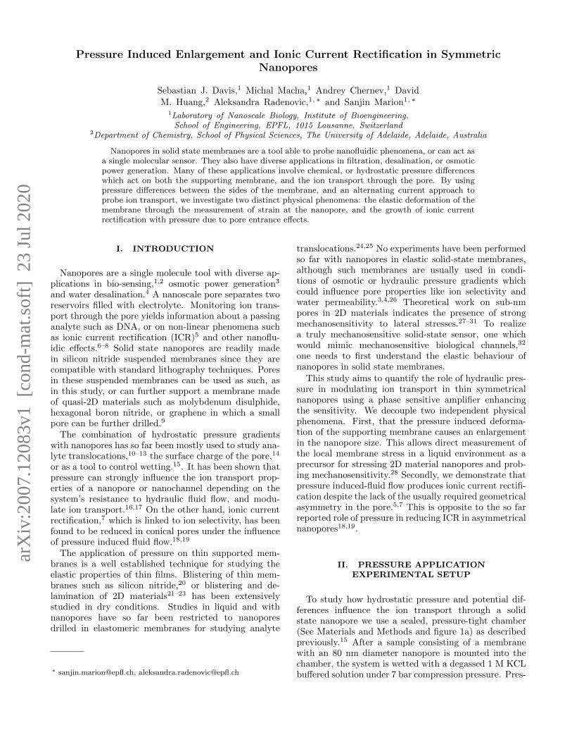
To study how hydrostatic pressure and potential dif-ferences influence the ion transport through a solidstate nanopore we use a sealed, pressure-tight chamber(See Materials and Methods and figure 1a) as describedpreviously.15 After a sample consisting of a membranewith an 80 nm diameter nanopore is mounted into thechamber, the system is wetted with a degassed 1 M KCLbuffered solution under 7 bar compression pressure. Pres-
FIG. 1: Application of pressure to solid state nanopores. a) Schematic in side view of the sealed pressure chamberchannels and electrical measurement. Zoom below shows the chip area and the convention of pressure sign chosen for this
study. b) DC IV curves for two representative samples having two different membrane sizes but similar pore sizes of d0 ≈ 80nm. Lines are linear fits giving resistance values of 1.5 MΩ and 1.7 MΩ. c) Mean values of resistance RAC as a function of
pressure normalized by the value of the resistance under no pressure RAC(P = 0). The curves represent the same samples asin panel (b) with two distinct square membrane sizes of side lengths a = 12 µm and 30 µm. Lines on the positive pressureside correspond to a fit to eq. 2 without residual stress giving a = 12.8 ± 1.0 µm, and a = 30.6 ± 6.2 µm respectively. The
corresponding total deflection of the membrane at P = 1500 mbar is w0 = 3.2 ± 0.8 µm, and 2.7 ± 0.6 µm respectively.
sure P is applied on the sample membrane using a mi-crofluidics pressure controller. We define positive pres-sure as being applied from the front-side of the membrane(flat side), and negative pressure is defined as being ap-plied from the back-side (etch-side) (as seen on figure1a). A potential difference V between the two sides ofthe membrane is applied and read with Ag/AgCl elec-trodes. Measurements of current I versus applied po-tential V are shown on figure 1b. Only samples showingstable conductance and current noise levels over the spanof the measurement were considered for further analysis(See Supporting information Sec. S2).
The current response of the nanopore to an external
potential difference V , and a pressure difference P be-tween the two sides of the membrane is of the formI = G(V, P )V + HsP , where Hs is the streaming con-ductance, and G(V, P ) the electrical conductance. Tak-ing into account that the non-linearity in conductanceis almost negligible (figure 1b), we perform a Taylor ex-pansion of the conductance G(V, P ) ≈ G1(P ) +G2(P )V ,with G1 and G2 corresponding to the linear and firstnonlinear contribution.15 The conductance term G1 hascontributions from the pore interior, and the access re-
gion resistance and obeys G1 = σ[4L/πd2 + 1/d
]−1,
where d is the diameter of the nanopore, L the thick-ness of the membrane, and σ the bulk conductance of
3
the solution.33,34 One measure of the nonlinearity in iontransport is the ionic current rectification (ICR) ratio5,7
which we define as:
r(V, P ) =|I(+V, P )− I(V = 0, P )||I(−V, P )− I(V = 0, P )|
≈ G1(P ) +G2(P )|V |G1(P )−G2(P )|V |
(1)
to exclude any streaming contribution.In order to deconvolute the linear and nonlinear ion
transport contributions of the nanopore, and eliminateany streaming current contribution, we perform all mea-surements using a quasi-static AC measurement. All ACmeasurements are performed using a sinusoidal voltage ata frequency of f = 1 Hz, where the resistance matches theDC measured value and no signal leakage through para-sitic chip capacitance is present.15 We use a phase sen-sitive amplifier, which can independently measure bothG1 and G2 by averaging out any components of the mea-sured current which are not at the base measurementfrequency f or one of its multiples. Thus the currentmeasured with the AC voltage does not have the stream-ing contribution included, and we obtain the total cur-rent which has two independently measured componentsI1 = G1(P )VAC and I2 = G2(P )V 2
AC, which are used tocalculate the ICR ratio r defined in equation 1. We there-fore perform AC measurements, with high precision, toextract the linear pore resistance RAC = G−11 , and theionic current rectification r at different pressures P (SeeSupporting information S2 for details).
III. STRAIN INDUCED PORE ENLARGEMENT
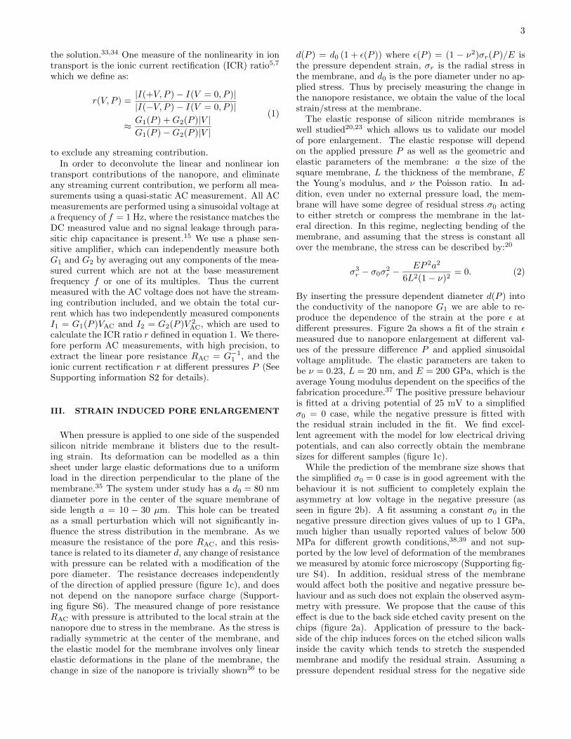
When pressure is applied to one side of the suspendedsilicon nitride membrane it blisters due to the result-ing strain. Its deformation can be modelled as a thinsheet under large elastic deformations due to a uniformload in the direction perpendicular to the plane of themembrane.35 The system under study has a d0 = 80 nmdiameter pore in the center of the square membrane ofside length a = 10 − 30 µm. This hole can be treatedas a small perturbation which will not significantly in-fluence the stress distribution in the membrane. As wemeasure the resistance of the pore RAC, and this resis-tance is related to its diameter d, any change of resistancewith pressure can be related with a modification of thepore diameter. The resistance decreases independentlyof the direction of applied pressure (figure 1c), and doesnot depend on the nanopore surface charge (Support-ing figure S6). The measured change of pore resistanceRAC with pressure is attributed to the local strain at thenanopore due to stress in the membrane. As the stress isradially symmetric at the center of the membrane, andthe elastic model for the membrane involves only linearelastic deformations in the plane of the membrane, thechange in size of the nanopore is trivially shown36 to be
d(P ) = d0 (1 + ε(P )) where ε(P ) = (1 − ν2)σr(P )/E isthe pressure dependent strain, σr is the radial stress inthe membrane, and d0 is the pore diameter under no ap-plied stress. Thus by precisely measuring the change inthe nanopore resistance, we obtain the value of the localstrain/stress at the membrane.
The elastic response of silicon nitride membranes iswell studied20,23 which allows us to validate our modelof pore enlargement. The elastic response will dependon the applied pressure P as well as the geometric andelastic parameters of the membrane: a the size of thesquare membrane, L the thickness of the membrane, Ethe Young’s modulus, and ν the Poisson ratio. In ad-dition, even under no external pressure load, the mem-brane will have some degree of residual stress σ0 actingto either stretch or compress the membrane in the lat-eral direction. In this regime, neglecting bending of themembrane, and assuming that the stress is constant allover the membrane, the stress can be described by:20
σ3r − σ0σ2
r −EP 2a2
6L2(1− ν)2= 0. (2)
By inserting the pressure dependent diameter d(P ) intothe conductivity of the nanopore G1 we are able to re-produce the dependence of the strain at the pore ε atdifferent pressures. Figure 2a shows a fit of the strain εmeasured due to nanopore enlargement at different val-ues of the pressure difference P and applied sinusoidalvoltage amplitude. The elastic parameters are taken tobe ν = 0.23, L = 20 nm, and E = 200 GPa, which is theaverage Young modulus dependent on the specifics of thefabrication procedure.37 The positive pressure behaviouris fitted at a driving potential of 25 mV to a simplifiedσ0 = 0 case, while the negative pressure is fitted withthe residual strain included in the fit. We find excel-lent agreement with the model for low electrical drivingpotentials, and can also correctly obtain the membranesizes for different samples (figure 1c).
While the prediction of the membrane size shows thatthe simplified σ0 = 0 case is in good agreement with thebehaviour it is not sufficient to completely explain theasymmetry at low voltage in the negative pressure (asseen in figure 2b). A fit assuming a constant σ0 in thenegative pressure direction gives values of up to 1 GPa,much higher than usually reported values of below 500MPa for different growth conditions,38,39 and not sup-ported by the low level of deformation of the membraneswe measured by atomic force microscopy (Supporting fig-ure S4). In addition, residual stress of the membranewould affect both the positive and negative pressure be-haviour and as such does not explain the observed asym-metry with pressure. We propose that the cause of thiseffect is due to the back side etched cavity present on thechips (figure 2a). Application of pressure to the back-side of the chip induces forces on the etched silicon wallsinside the cavity which tends to stretch the suspendedmembrane and modify the residual strain. Assuming apressure dependent residual stress for the negative side
4
x103
-2
-4
0 0.1 0.2(VAC)2 [V2]
0.3
a) b)
c)
25 mV400 mV800 mV
α
0 0.5 1.0
Pressure [bar]1.5-0.5-1.0-1.5
1.000
1.010
1.015
1.020
1.025
1 +
ε-6
FIG. 2: Elastic response of membranes under pressure: strain induced enlargement. a) Schematic of the chip andmembrane with nanopore. The initial configuration under zero applied pressure is shown as well as two schematics showingthe deformation of the membrane under both positive, and negative pressure. This deformation due to strain enlarges the
pore, d(−P ) and d(+P ). The negative pressure is also shown to act on the etched walls of the back-side of the chip which isresponsible for the asymmetry in pressure response. b) Normalised strain value as a function of pressure for the samemembrane at a low bias voltage of VAC = 25 mV (blue squares), and two larger bias voltages of VAC = 400 mV (green
triangles), and V0 = 800 mV (red circles). All AC voltages are given in root mean square values of the amplitude. Dashedblack lines correspond to the fit of the stress to Eq. (2). For positive pressures the fit is done with σ0 = 0 fixed, and for the
negative side with the full stress eq. (2). c) Voltage dependence of the residual stress factor α with the dashed linecorresponding to a quadratic fit to applied voltage VAC. Error bars represent the standard deviation as obtained from the fit.
of the form σ0 = αP we find a value of α ≈ −6000 atthe lowest applied sinusoidal potential for negative pres-sures (figure 2c). This value can be rationalised fromgeometrical considerations. The applied pressure will in-duce a force Fin ∝ LSiP sin(54, 74), where LSi = 380µm is the thickness of the silicon substrate, with the an-gle 54, 74 defined by crystallographic planes. This esti-mate gives a comparable induced residual stress factor ofα ≈ LSi sin(54)/L ≈ −10000 while neglecting any fineeffects dependent on the manufacturing process.
Although including a pressure dependent residualstress on the negative pressure side explains most of themeasured behaviour, figure 2c shows that the inducedresidual stress factor α depends quadratically on theapplied voltage. We propose that this effect is due toelectrostriction of the underlying chip material which isknown to occur for all dielectrics at high electric field re-gardless of crystal symmetry.40,41 Considering the thick-ness of the materials in question, the electric field at 800mV RMS is on the order of 2 kV/m over the silicon sub-strate and on the order of 40 MV/m over the 20 nmthick silicon nitride membrane, sufficient to produce sev-
eral percent of strain due to electrostriction. This stresscounterbalances the pressure induced residual stress dis-cussed above returning a symmetric pressure profile athigh voltage. At large voltages the measured data devi-ates from the model and we assume that the stresses inthese cases are no longer within the range of validity ofeq. 2.
IV. PRESSURE INDUCED IONIC CURRENTRECTIFICATION
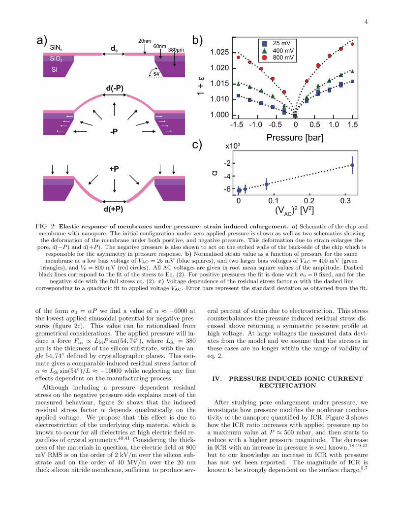
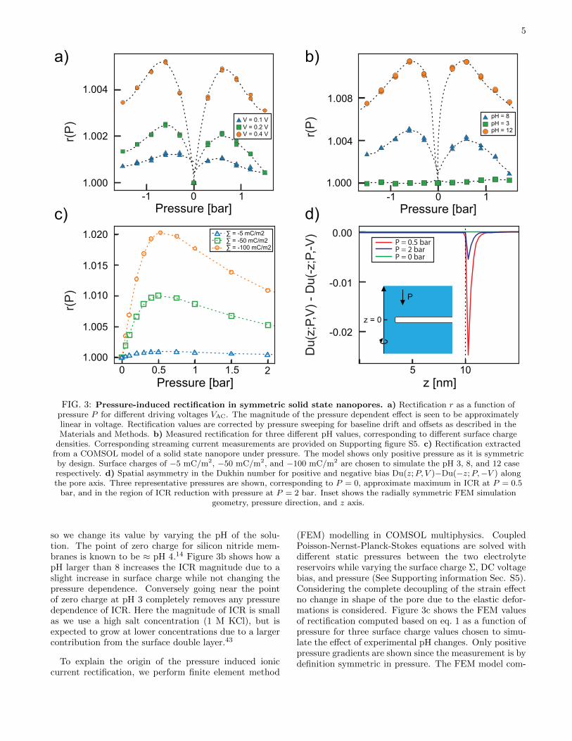
After studying pore enlargement under pressure, weinvestigate how pressure modifies the nonlinear conduc-tivity of the nanopore quantified by ICR. Figure 3 showshow the ICR ratio increases with applied pressure up toa maximum value at P ≈ 500 mbar, and then starts toreduce with a higher pressure magnitude. The decreasein ICR with an increase in pressure is well known,18,19,42
but to our knowledge an increase in ICR with pressurehas not yet been reported. The magnitude of ICR isknown to be strongly dependent on the surface charge,5,7
5
a)
c) d)
b)
∑ = -5 mC/m2 ∑ = -50 mC/m2 ∑ = -100 mC/m2
pH = 8 pH = 3 pH = 12
V = 0.1 VV = 0.2 VV = 0.4 V
-1 0Pressure [bar]
1
0 0.5Pressure [bar]
1 1.5 2
-1 0Pressure [bar]
1
5 10z [nm]
r(P
)
1.000
1.002
1.004
r(P
)
1.000
1.005
1.010
1.015
1.020
r(P
)
1.000
1.004
1.008
Du(
z;P,
V) -
Du(
-z;P
,-V)
-0.01
-0.02
0.00P = 2 barP = 0.5 bar
P = 0 bar
z = 0
P
FIG. 3: Pressure-induced rectification in symmetric solid state nanopores. a) Rectification r as a function ofpressure P for different driving voltages VAC. The magnitude of the pressure dependent effect is seen to be approximatelylinear in voltage. Rectification values are corrected by pressure sweeping for baseline drift and offsets as described in theMaterials and Methods. b) Measured rectification for three different pH values, corresponding to different surface charge
densities. Corresponding streaming current measurements are provided on Supporting figure S5. c) Rectification extractedfrom a COMSOL model of a solid state nanopore under pressure. The model shows only positive pressure as it is symmetricby design. Surface charges of −5 mC/m2, −50 mC/m2, and −100 mC/m2 are chosen to simulate the pH 3, 8, and 12 caserespectively. d) Spatial asymmetry in the Dukhin number for positive and negative bias Du(z;P, V )−Du(−z;P,−V ) alongthe pore axis. Three representative pressures are shown, corresponding to P = 0, approximate maximum in ICR at P = 0.5
bar, and in the region of ICR reduction with pressure at P = 2 bar. Inset shows the radially symmetric FEM simulationgeometry, pressure direction, and z axis.
so we change its value by varying the pH of the solu-tion. The point of zero charge for silicon nitride mem-branes is known to be ≈ pH 4.14 Figure 3b shows how apH larger than 8 increases the ICR magnitude due to aslight increase in surface charge while not changing thepressure dependence. Conversely going near the pointof zero charge at pH 3 completely removes any pressuredependence of ICR. Here the magnitude of ICR is smallas we use a high salt concentration (1 M KCl), but isexpected to grow at lower concentrations due to a largercontribution from the surface double layer.43
To explain the origin of the pressure induced ioniccurrent rectification, we perform finite element method
(FEM) modelling in COMSOL multiphysics. CoupledPoisson-Nernst-Planck-Stokes equations are solved withdifferent static pressures between the two electrolytereservoirs while varying the surface charge Σ, DC voltagebias, and pressure (See Supporting information Sec. S5).Considering the complete decoupling of the strain effectno change in shape of the pore due to the elastic defor-mations is considered. Figure 3c shows the FEM valuesof rectification computed based on eq. 1 as a function ofpressure for three surface charge values chosen to simu-late the effect of experimental pH changes. Only positivepressure gradients are shown since the measurement is bydefinition symmetric in pressure. The FEM model com-
6
pletely captures the behaviour seen in the experimentaldata on figure 3b, with an increase in r at low pressuresbefore a turnover and decrease at higher pressures. Themeasured decrease in magnitude of the effect as the sur-face charge is reduced is also captured.
The rectification behaviour can be rationalised interms of perturbations to the ion distributions in andaround the nanopore caused by pressure-induced advec-tion. ICR in a nanapore has been shown previously to becontrolled by the spatial variation in the axial direction zof the local Dukhin number Du(z), with stronger asym-metry of Du(z) between the pore ends yielding strongerrectification.7 The Dukhin number measures the relativemagnitude of surface to bulk ionic conduction. For a1:1 electrolyte, and in the absence of Debye layer overlap
in the pore, Du(z) = − 〈c+(z)−c−(z)〉2(c+(z,r=0)+c−(z,r=0)) , where c±
are the positive and negative ion concentrations, 〈· · · 〉denotes an average over the pore cross-section, and r isthe radial coordinate.7 Pressure-driven flow induces spa-tial asymmetry in Du(z) since conservation of ion cur-rent as the bulk solution is transported into the chargednanopore perturbs both the local ionic charge densitync = e(c+ − c−), and local total ion concentrationctot = c+ + c− (Supplemental figures S8 and S9 respec-tively), particularly when coupled with the applied elec-tric field. At sufficiently high pressures, however, con-vection completely replaces the fluid inside the nanoporeby the bulk solution, reducing the spatial variation ofDu(z) and diminishing ICR, as observed in both experi-ments and FEM simulations. The spatial asymmetry ofDu(z) at positive versus negative bias ±V for differentpressures P from the FEM simulations is quantified byDu(z;P, V )−Du(−z;P,−V ) in figure 3d, which confirmsthat the asymmetry is greatest at an intermediate pres-sure corresponding to the strongest rectification.
The pressure-induced asymmetry in Du(z) is localizedto the pore ends in the FEM simulations (figure 3d).Thus, rectification is expected to be controlled by a di-mensionless Peclet number Pe = ud
D quantifying the rel-ative importance of ion advection compared with diffu-sion in which the characteristic length scale is the porediameter d. Here u is the average pressure-driven fluidvelocity and D the diffusivity of the ions (which is ap-proximately the same for K+ and Cl−). Rectification isexpected to be pronounced for Pe > 1 and to diminishas Pe→∞. Consistent with this picture, the maximumrectification factor in the experiments and FEM simula-tions (at P ≈ 500 mbar) occurs at Pe ≈ 7, if we take
u ≈ d2P2η(16L+3πd) ,
44 the average fluid velocity magnitude
across a nanopore of length L and diameter d for fluidviscosity η due to an applied pressure P and use the ex-perimental/simulation parameter values.
V. CONCLUSIONS
By coupling a nanopore inside a thin elastic supportedsilicon nitride membrane immersed in liquid, we demon-strated how one can use AC measurements of ion trans-port coupled with hydrostatic pressure to precisely mea-sure two separate physical phenomena. By monitoringthe size of a nanopore while the membrane is undergoingpressure induced blistering, we demonstrate that one canprecisely measure local strain in the membrane. As thesemembranes are typically used as a support for 2D mate-rial nanopore measurements, this can be the first step inmeasuring mechanosensitivity in 2D materials27–31 as itallows calibration and control of applied stresses. Stressin the 2D membrane under deformation is expected tocause restructuring of the bonds in the nanopore edges,opening up a pathway for ion transport, in direct anal-ogy to biological ion channels.32 This could provide astress-sensitive alternative to the newly reported pres-sure sensitive ion transpor behaviour in single digit car-bon nanotubes.17 In addition to strain induced enlarge-ment of nanopores, we have shown how thin nanoporescan induce nonlinear transport phenomena such as ioniccurrent rectification. This is in contrast to the so far re-ported effect of the reduction of ICR with pressure.18,19
Similar to systems which have liquid flow slippage, likelong carbon nanotubes17, or angstrom slits16, membranesin almost-2D membranes have low hydraulic resistancewhich, along with access effects, produces novel nonlin-ear nanofluidic phenomena.
SUPPORTING INFORMATION
The supporting information contains the Materials andmethods section, details about the strain and ionic cur-rent rectification measurements and FEM model detailswith additional plots.
AUTHOR CONTRIBUTIONS
S.J.D. performed the experiments, analysed the dataand performed FEM simulations. S.M. designed andbuilt the experimental set-up and built the FEM model.M.M. designed the microfluidic chamber and performedAFM imaging. A.C. fabricated devices. A.R. and S.M.supervised the research. D.M.H. provided an explanationfor the ionic current rectification. S.J.D. and S.M. wrotethe manuscript with all authors providing important sug-gestions for the experiments, discussing the results, andcontributing to the manuscript.
ACKNOWLEDGEMENT
The authors thank Marko Popovic and Alex Smolyan-itsky for useful discussions on the membrane elas-
7
ticity. This work was financially supported by theSwiss National Science Foundation (SNSF) Consolida-tor grant (BIONIC BSCGI0 157802) and from the Euro-
pean Union’s Horizon 2020 research and innovation pro-gramme under the Marie Skodowska-Curie grant agree-ment No 754462.
[1] C. Plesa, S. W. Kowalczyk, R. Zinsmeester, A. Y. Gros-berg, Y. Rabin, and C. Dekker, Nano Lett. 13, 658(2013).
[2] C. A. Merchant, K. Healy, M. Wanunu, V. Ray, N. Pe-terman, J. Bartel, M. D. Fischbein, K. Venta, Z. Luo,A. T. C. Johnson, and M. Drndic, Nano Lett. 10, 2915(2010).
[3] M. Macha, S. Marion, V. V. R. Nandigana, and A. Rade-novic, Nat. Rev. Mater. 4, 588 (2019).
[4] R. Epsztein, R. M. DuChanois, C. L. Ritt, A. Noy,and M. Elimelech, Nat. Nanotechnol. (2020),10.1038/s41565-020-0713-6.
[5] Z. Siwy, Adv. Funct. Mater. 16, 735 (2006).[6] S. Gravelle and C. Ybert, J. Chem. Phys. 151, 244503
(2019).[7] A. R. Poggioli, A. Siria, and L. Bocquet, J. Phys. Chem.
B 123, 1171 (2019).[8] L. Bocquet and E. Charlaix, Chem. Soc. Rev. 39, 1073
(2010).[9] M. Graf, M. Lihter, M. Thakur, V. Georgiou, J. Topolan-
cik, B. R. Ilic, K. Liu, J. Feng, Y. Astier, and A. Rade-novic, Nat. Protoc. 14, 1130 (2019).
[10] H. Zhang, Q. Zhao, Z. Tang, S. Liu, Q. Li, Z. Fan,F. Yang, L. You, X. Li, J. Zhang, and D. Yu, Small9, 4112 (2013).
[11] B. Lu, D. P. Hoogerheide, Q. Zhao, H. Zhang, Z. Tang,D. Yu, and J. A. Golovchenko, Nano Lett. 13, 3048(2013).
[12] J. Li, R. Hu, X. Li, X. Tong, D. Yu, and Q. Zhao,Electrophoresis 38 (2017), 10.1002/elps.201600410.
[13] D. P. Hoogerheide, B. Lu, and J. A. Golovchenko, ACSNano 8, 7384 (2014).
[14] M. Firnkes, D. Pedone, J. Knezevic, M. Doblinger, andU. Rant, Nano Lett. 10, 2162 (2010).
[15] S. Marion, M. Macha, S. J. Davis, A. Chernev, andA. Radenovic, arXiv e-prints , arXiv:1911.05229 (2019).
[16] T. Mouterde, A. Keerthi, A. R. Poggioli, S. A. Dar,A. Siria, A. K. Geim, L. Bocquet, and B. Radha, Nature567, 87 (2019).
[17] A. Marcotte, T. Mouterde, A. Nigues, A. Siria, andL. Bocquet, Nat. Mater. (2020), 10.1038/s41563-020-0726-4.
[18] W.-J. Lan, D. A. Holden, and H. S. White, J. Am. Chem.Soc. 133, 13300 (2011).
[19] L. Jubin, A. Poggioli, A. Siria, and L. Bocquet, Proc.Natl. Acad. Sci. 115, 4063 (2018).
[20] J. Vlassak and W. Nix, J. Mater. Res. 7, 3242 (1992).
[21] S. P. Koenig, N. G. Boddeti, M. L. Dunn, and J. S.Bunch, Nat. Nanotechnol. 6, 543 (2011).
[22] N. G. Boddeti, X. Liu, R. Long, J. Xiao, J. S. Bunch,and M. L. Dunn, Nano Lett. 13, 6216 (2013).
[23] J. S. Bunch, S. S. Verbridge, J. S. Alden, A. M. van derZande, J. M. Parpia, H. G. Craighead, and P. L.McEuen, Nano Lett. 8, 2458 (2008).
[24] G. R. Willmott and P. W. Moore, Nanotechnology 19,475504 (2008).
[25] G. S. Roberts, D. Kozak, W. Anderson, M. F. Broom,R. Vogel, and M. Trau, Small 6, 2653 (2010).
[26] T. Humplik, J. Lee, S. C. O’Hern, B. A. Fellman, M. A.Baig, S. F. Hassan, M. A. Atieh, F. Rahman, T. Laoui,R. Karnik, and E. N. Wang, Nanotechnology 22, 292001(2011).
[27] W. Li, Y. Yang, J. K. Weber, G. Zhang, and R. Zhou,ACS Nano 10, 1829 (2016).
[28] A. Fang, K. Kroenlein, and A. Smolyanitsky, J. Phys.Chem. C 123, 3588 (2019).
[29] S. Sahu, J. Elenewski, C. Rohmann, and M. Zwolak, Sci.Adv. 5 (2019), 10.1126/sciadv.aaw5478.
[30] A. Fang, K. Kroenlein, D. Riccardi, and A. Smolyanit-sky, Nat. Mater. 18, 76 (2019).
[31] A. Smolyanitsky, A. Fang, A. F. Kazakov, andE. Paulechka, Nanoscale 12, 10328 (2020).
[32] C. D. Cox, N. Bavi, and B. Martinac, Cell Rep. 29, 1(2019).
[33] J. E. Hall, J. Gen. Physiol. 66, 531 (1975).[34] S. W. Kowalczyk, A. Y. Grosberg, Y. Rabin, and
C. Dekker, Nanotechnology 22, 315101 (2011).[35] S. P. Timoshenko and S. Woinowsky-krieger (McGraw-
Hill, 1959).[36] N. A. Dye, M. Popovic, K. V. Iyer, S. Eaton, and
F. Julicher, bioRxiv (2020), 10.1101/2020.04.16.044883.[37] L. Buchaillot, E. Farnault, M. Hoummady, and H. Fu-
jita, Jpn. J. Appl. Phys. 36, L794 (1997).[38] P. Temple-Boyer, C. Rossi, E. Saint-Etienne, and
E. Scheid, J. Vac. Sci. Technol. A 16, 2003 (1998).[39] A. Noskov, E. Gorokhov, G. Sokolova, E. Trukhanov,
and S. Stenin, Thin Solid Films 162, 129 (1988).[40] S. W. P. van Sterkenburg, J. Phys. D: Appl. Phys 25,
996 (1992).[41] F. Blaffart, Q. Van Overmeere, T. Pardoen, and
J. Proost, J. Solid State Electr. 17, 1945 (2013).[42] W.-J. Lan, M. A. Edwards, L. Luo, R. T. Perera, X. Wu,
C. R. Martin, and H. S. White, Acc. Chem. Res. 49,2605 (2016).
[43] C. Lee, L. Joly, A. Siria, A.-L. Biance, R. Fulcrand, andL. Bocquet, Nano Lett. 12, 4037 (2012).
[44] H. L. Weissberg, Phys. Fluids 5, 1033 (1962).

![Irving Chernev[1]](https://static.documents.pub/doc/80x56/55cf8fc2550346703b9f883c/irving-chernev1.jpg)


