APPLIED PHYSICS LETTERS 90,042901 (2007) Second harmonic generation and ferroelectric phase transitions in thick and ultrathin Pbo.3sSro.ssTi03 films on (001) MgO substrates S. W. ~iu,~' J. Chakhalian, and Min xiaob' Department of Physics, Universiry of Arkansas, Fayettel~ille, Arkansas 72701 C. L. Chen Departnlent of Pl~ysics and Astrononiy, University of Texas at Sun Antonio, San Airtonio, Texns 78249 (Received 12 June 2006; accepted 17 December 2006; published online 22 January 2007) Second harmonic generation of a 16-nm-thick ultrathin Pbo,,5Sro,65Ti03 film and a 243-nm-thick Pb0,35Sr0,65Ti03 film grown on (001) MgO substrates by pulsed laser deposition is investigated. It is concluded that in the ultrathin film the ferroelectric phase is still present and the diffuse phase transition is absent. In contrast, the thick film exhibits a pronounced diffuse phase transition. Theoretical analysis based on the polarization diagrams shows that the compensated c-domain fraction is dorni~~ant in both films whereas the nonlinear susceptibility of the ultrathin film has a different tensor property from the thick film. 0 2007 American Institute of Physics. [DOI: l0.1063/1.2333023] Ferroelectric thin film have been considered to be very promising materials for a number of applications. These ap- plications are usually related to their large nonlinear re- sponses to the electromagnetic radiation from microwave to optical light. These effects include microwave tunability, electro-optic effect, nonlinear optical absorption and refrac- tion, second harmonic generation (SHG), etc. Especially, SHG process has also been widely used as a highly sensitive probe to study the interfacial, surface, and thin film phenom- ena because the efficiency of SHG is highly dependent on the materials' structural symmetry.' For a typical perovskite ferroelectric material such as PbTi03 with a centrosymmetric cubic symmetry in the paraelectric state, the bulk contribu- tion to SHG is absent in the electric-dipole approximation above the Curie temperature. Upon coolillg PbTi03 under- goes a sharp structural phase transition to ferroelectric state by lowering its symmetry from centrosymmetric cubic to polar tetragonal. This symmetry breaking process produces a dramatic change in SHG efficiency. Recently, ferroelectric Pb0.35Sr0,65Ti03 (PST) thin films have been regarded as an important candidate for the room temperature tunable microwave devices such as microwave phase shifters because of its high dielectric constant and large tunability."' In this compound a partial substitution of pb2+ by S I ~ + results in a pronounced diffuse phase transition observed in both ceramics and single-crystal specimens."6 The diffuse phase transition in ferroelectrics is characterized by a broadened phase transition in a wide temperature inter- val (so called Curie range) around the temperature (T,,,) where the dielectric permittivity assumes its maximum value and shows the most remarkable relaxor features such as small dielectric hysteresis or dielectric anhysteresis within the transition range. It is the suppression or lack of the di- electric hysteresis that makes the relaxor compounds useful in the tunable microwave devices with precise tunability. Similar phenomena have been observed in some other ferroelectrics via dielectric measurements including (B~,s~)T~o,,'~"~(T~,s~)o~~ P~(M~,,~N~~~)O~,'~ C~C. Such thermally broadened phase transition has generally "'~lectronic mail: sx1030uark.edu b'~lectronic mail: [email protected]been attributed to the presence of the nanopolar clusters that may be detected by the method of SHG. In addition, the size effect in the ferroclectrics has currently attracted consider- able experimental and theoretical attention and remains a challenging issue because the ferroelectricity is strongly in- fluenced by the external effects such as composition, strain, and dislocation."-'' As a noncontacr and highly sensitive technique, optical SHG is a more convenient probe of ferro- electricity bccause it avoids disturbing effects (such as "dead-layer'' effectsL4) from electrodes compared to the con- ventional dielectric nleasureinents. In this letter, we present the first SHG measurements of the novel PST films. The domain structures and thc nonlinear susceptibility were ana- lyzed by measuring the polarization diagrams of SHG for both thick and ultrathin Pb0,35Sr065Ti03 thin films. We have investigated the ferroelectricity for both thick and ultrathin Pb0,35Sr0,65Ti03 thin films by measuring SHG intensity in a wide temperature range of 78-380 K. We observed the FIG. 1. Schematic diagram of the experimental configuration. The funda- mental light of frequency (0 (810 nm) is incident under 45" to the normal [001] of the PSTlMgO sample (i.e., incident in the [~ii] direction), and the SH radiation is observed under specular reflection h e . , in the [ o i l ] direc- tion). Inset: The relevant crystallographic directions. LF, long-pa5s filter; X12, half-wave plate; BF, bandpass filter; and P, Glan polarizer. 0003-6951 /2007/90(4)/042901/3/$23.00 90.042901-1 @ 2007 American Institute of Physics Downloaded 25 Mar 2OQ8 to 130.184.237.6. Redistrlbutlonsubject to AIP license or copyright; see http:Napl.a1p.orglapI1copyr1ght,jsp
Transcript
APPLIED PHYSICS LETTERS 90,042901 (2007)
Second harmonic generation and ferroelectric phase transitions in thick and ultrathin Pbo.3sSro.ssTi03 films on (001) MgO substrates
S. W. ~ i u , ~ ' J. Chakhalian, and Min xiaob' Department of Physics, Universiry of Arkansas, Fayettel~ille, Arkansas 72701
C. L. Chen Departnlent of Pl~ysics and Astrononiy, University of Texas at Sun Antonio, San Airtonio, Texns 78249
(Received 12 June 2006; accepted 17 December 2006; published online 22 January 2007)
Second harmonic generation of a 16-nm-thick ultrathin Pbo,,5Sro,65Ti03 film and a 243-nm-thick Pb0,35Sr0,65Ti03 film grown on (001) MgO substrates by pulsed laser deposition is investigated. It is concluded that in the ultrathin film the ferroelectric phase is still present and the diffuse phase transition is absent. In contrast, the thick film exhibits a pronounced diffuse phase transition. Theoretical analysis based on the polarization diagrams shows that the compensated c-domain fraction is dorni~~ant in both films whereas the nonlinear susceptibility of the ultrathin film has a different tensor property from the thick film. 0 2007 American Institute of Physics. [DOI: l0.1063/1.2333023]
Ferroelectric thin f i l m have been considered to be very promising materials for a number of applications. These ap- plications are usually related to their large nonlinear re- sponses to the electromagnetic radiation from microwave to optical light. These effects include microwave tunability, electro-optic effect, nonlinear optical absorption and refrac- tion, second harmonic generation (SHG), etc. Especially, SHG process has also been widely used as a highly sensitive probe to study the interfacial, surface, and thin film phenom- ena because the efficiency of SHG is highly dependent on the materials' structural symmetry.' For a typical perovskite ferroelectric material such as PbTi03 with a centrosymmetric cubic symmetry in the paraelectric state, the bulk contribu- tion to SHG is absent in the electric-dipole approximation above the Curie temperature. Upon coolillg PbTi03 under- goes a sharp structural phase transition to ferroelectric state by lowering its symmetry from centrosymmetric cubic to polar tetragonal. This symmetry breaking process produces a dramatic change in SHG efficiency.
Recently, ferroelectric Pb0.35Sr0,65Ti03 (PST) thin films have been regarded as an important candidate for the room temperature tunable microwave devices such as microwave phase shifters because of its high dielectric constant and large tunability."' In this compound a partial substitution of pb2+ by S I ~ + results in a pronounced diffuse phase transition observed in both ceramics and single-crystal specimens."6 The diffuse phase transition in ferroelectrics is characterized by a broadened phase transition in a wide temperature inter- val (so called Curie range) around the temperature (T,,,) where the dielectric permittivity assumes its maximum value and shows the most remarkable relaxor features such as small dielectric hysteresis or dielectric anhysteresis within the transition range. It is the suppression or lack of the di- electric hysteresis that makes the relaxor compounds useful in the tunable microwave devices with precise tunability. Similar phenomena have been observed in some other ferroelectrics via dielectric measurements including ( B ~ , s ~ ) T ~ o , , ' ~ " ~ ( T ~ , s ~ ) o ~ ~ P ~ ( M ~ , , ~ N ~ ~ ~ ) O ~ , ' ~ C ~ C . Such thermally broadened phase transition has generally
been attributed to the presence of the nanopolar clusters that may be detected by the method of SHG. In addition, the size effect in the ferroclectrics has currently attracted consider- able experimental and theoretical attention and remains a challenging issue because the ferroelectricity is strongly in- fluenced by the external effects such as composition, strain, and dislocation."-'' As a noncontacr and highly sensitive technique, optical SHG is a more convenient probe of ferro- electricity bccause it avoids disturbing effects (such as "dead-layer'' effectsL4) from electrodes compared to the con- ventional dielectric nleasureinents. In this letter, we present the first SHG measurements of the novel PST films. The domain structures and thc nonlinear susceptibility were ana- lyzed by measuring the polarization diagrams of SHG for both thick and ultrathin Pb0,35Sr065Ti03 thin films. We have investigated the ferroelectricity for both thick and ultrathin Pb0,35Sr0,65Ti03 thin films by measuring SHG intensity in a wide temperature range of 78-380 K. We observed the
FIG. 1. Schematic diagram of the experimental configuration. The funda- mental light of frequency (0 (810 nm) is incident under 45" to the normal [001] of the PSTlMgO sample (i.e., incident in the [~ii] direction), and the SH radiation is observed under specular reflection he . , in the [ o i l ] direc- tion). Inset: The relevant crystallographic directions. LF, long-pa5s filter; X12, half-wave plate; BF, bandpass filter; and P, Glan polarizer.
0003-6951 /2007/90(4)/042901/3/$23.00 90.042901-1 @ 2007 American Institute of Physics Downloaded 25 Mar 2OQ8 to 130.184.237.6. Redistrlbutlon subject to AIP license or copyright; see http:Napl.a1p.orglapI1copyr1ght,jsp
Journul of Modern Optics +, Taylor &Francis V O ~ . 54, NOS. 16-17, 10-20 November 2007, 2441-2450 0 Taylor E. Francis croup
Stochastic resonance with multiplicative noise in a three-level atomic bistable system
HAIBIN WU, AMITABH JOSH1 and MIN XIAO*
Department of Physics, University of Arkansas, Fayetteville, Arkansas 72701, USA
(Received 22 February 2007; i~iJnalform 29 August 2007)
We experimentally investigate stochastic resonance phenomenon with multi- plicative noise in a A-type three-level atomic bistable system. The system perturbed by a periodic low frequency forcing term shows an improved signal- to-noise ratio at certain strength of the multiplicative noise applied onto the cavity frequency.
Stochastic resonance (SR) [l-31 has bee11 the subject of intensive research interest in past decades. It has been explored in a wide variety of physical systems, such as bistable ring lasers [4], nanomechanical systems [5], electronic and magnetic systems [6 ] , and biological and neuronal systems [7-101. With an external periodic perturbation applied to such two-state nonlinear systems, an addition of noise to the input of the system can induce synchronized jumps between the two stable states, showing a resonance-like peak behaviour in the signal-to-noise ratio (SNR) for certain noise strength when the noise level is scanned. Under certain conditions increasing the disorder of the input noise in a two-state nonlinear system can actually lead to an increase in the order of the output (i.e. improved SNR). It is well established that for three-level atoms, the Kerr nonlinear refractive index can be greatly enhanced due to the induced atomic coherence accompanying with reduced linear absorption [ll] , which can substantially modify the thresholds of the atomic optical bistability (AOB) and switching time between the bistable steady states, and control the width and height of the double-well potential (the shape of the bistable curves) [12]. These features, together with the high stability and reproducibility in the experimental setup, make the system an ideal candidate to study the detail characteristics of the SR. Studying SR in such multi-level atomic systems can help our understanding of the noise properties in these systems, and hopefully lead to new techniques to improve small signal detection and information processing in such coherent atomic systems. We have experinlentally demonstrated the SR
*Corresponding author. Email: mxiao(iuark.edu
Jorfrnul of Modern Oprics ISSN 095W340 print/ISSN 1362-3044 online :Q 2007 Taylor & Francis
Controlling four-wave and six-wave mixing processes in multilevel atomic systems
Yanpeng hang,^! Utsab Khadka, Blake Anderson, and Min xiaob' Department of Physics, University of Arkansas, Fayetteville, Arkat~sas 72701, USA
(Received 10 September 2007; accepted 4 November 2007; published online 29 November 2007)
We experimentally demonstrate that four-wave mixing (FWM) and six-wave mixing (SWM) processes can be selectively turned on and off in a close-cycled four-level atomic system. Under certain laser beam configuration, the FWM and SWM processes can be made to coexist with similar signal amplitudes and transmit through the same electromagnetically induced transparency window in such folded four-level atomic system. By introducing an additional pumping laser beam connecting to the fifth energy level, both FWM and SWM signals can be greatly enhanced. 0 2007 American Iflstit~rte of Physics. [DOI: 10,106311.28 177441
Although four-wave mixing (FWM) and six-wave mix- ing (SWM) processes have becn individually observed in close-cycled (folded) multilevel atomic systems in the past few years,'-' the coexisting FWM and SWM have, so far, only been observed in open-cycled multilevel (such as Y-types and inverted Y-typeb) atomic systems. In these open- cycled multilevel atomic systems, the FWM and SWM sig- nals can be simultaneously generated via transitions in dif- ferent branches associated with different electromagnetically induced transparencyxg (EIT) indows, which can be sepa- rated (or placed together to overlap) in frequency by adjust- ing the frequency detunings of various coupling laser beams.'."he atomic coherence effect IS the key to enhance the magnitude of the higher-order SWM signal to be compa- rable to the FWM signal (which is suppressed at the same time), so the interference between the FWM and SWM sig- nals can be experimentally observed.
In the close-cycled (or folded) four-level atomic system, as shown in Fig. I (a), the SWM process (via the path
0 1 Y -0J3 -Y 10) - lI)-l2)-13) -12) - (1)
-'"I - (0)) will have to go through the FWM path 0 1 Y -9 - 0 1
(10) - 11) - (2) - 11) - lo)).' So when an efficient FWM process with one weak probe beam E l (w,, k l , and Rabi frequency GI , connecting transition 10) and 11)) and two coupling laser beams (E2 with w2, k2, and Rabi frequency G2 and E; with w2, k;, and Rabi frequency Gi, connecting upper transition (1) and (2)) exists, it will dominate the wave-mixing processes since the SWM process will be several orders of magnitude smaller than the FWM signal in such case even when the strong fields E?
gether with Ej and E; (for transition (2) and 13)), both FWM and SWM processes can be generated simultaneously and, with appropriate conditions, made to be in similar magni- tudes. TO ~xperimentally demonstrate different wave-mixing processes, such as pure FWM, pure SWM, coexisting FWM and SWM, as well as dressed FWM. different coupling laser beams will be blocked during the experiments. Also, when an additional pumping h e r beam E4 (w4, connecting transi- tion 14) to 13)) is turned on, as shown in Fig. l(b), the dressed-FWM and SWM signals can bc greatly enhanced, indicating optical pumping, as well as dressed-SWM effect. One ladder-type EIT subsystem will form between transi- tions IO)-t(1)-+12) and an EIT window appears [bottom curve of Fig. 2(a), labeled as P],~ which depends on the frequency detuning A, (Ai=Qi- wi with atomic resonant fre- quency Ai for the corresponding transition). The generated multiwave mixing (MWM) signals at frequency wl all fall into this EIT window and can pass through the medium with reduced absorption. To spatially separate these generated MWM signals from the probe beam El and satisfy the phase- matching condit ions and two-photon ~ o ~ ~ l e r - f r e e ~ o n f i ~ u r a t i o n s ~ ' ~ the laser beams are aligned spatially in the square-box pattern shown in Fig. I (ci, with five laser beams (E2, E;, E, , Ej, E4) propagating through the atomic medium in the same direction with small angles (-0.3") between them. The probe beam E, propagates in the opposite direc- tion. The generated MWM signals are then all propagating in one direction labeled as EM ill Fig. l(c).
The experimental demonstration of coexisting MWM processes through one EIT window was carried out in atomic vapor of 8 5 ~ b . The energy levels of 5slI2(F=3), 5p3,?, 5d312,
(w3, k3, and Rabi frequency G3) and E; (w3, k;, and ~ a b i frequcncy G;) (connecting transition (2) to (3)) are present. However, one can turn off the dominant FWM blocking either E2 or E; beam, in which case the system
'An
as demonstrated in Refs. 4. (c)
In this letter, we show that by using a strong E2 and a weaker E; (E; E2) for the upper transitioll (1) and (2), to- FIG. I. (a) Folded four-level atomic system for generating FWM and SWM
processes (E;< E,). (b) The folded five-level atomic system with an addi- tional pumping beam E, (the dashed arrow). (c) Square box-pattern beam
a)~~ectrollic mail: ypzhang8mail.xjtu.edu.cn. geometry used in the experiment. The dash-dotted mows are the generated b)~lectronic mail: [email protected]. MWM signals.
0003-69~1/2~~7~91(22)/221108/~/$23.00 91,221108-1 O 2007 American Institute of Physi~a Downloaded 25 Mar 2668 to 130.164.237.6. Redistribution subject to AIP license or copyright; see http:llapl.alp.orglapIIEopyrigl~t.jsp
@ Indian Academy of f3ciences Vol. 69, No. 2 Auguat 2007 pp. 219-228
Single-photon all-optical switching using coupled microring resonators
WENGE YANG*, AMITABH JOSH1 and MIN XIAO Department of Phpica, Univemity of Ark-, Fbyetteville, AR 72701, USA 'Current addrees: School of Engineering, Unimity of CA, Smta Crua, 1156 High Street, Santa Cruz, CA, 95084, USA Email: wyan&soe.uesc.edu; ajoshiOuark.edu
MS received 21 January 2007; reviaed 18 April 2007; accepted 7 May 2007
Abstract. We study the nonlinear phaee reepom of a microring reeonator coupled to a bw waveguide and the use of thin nonlinear phase shift to store information in the microring resonetor and enhance the switching characteriatlca of a Mach-Zehnder interferometer (MZI). By introducing coupling between adjacent microring resonators, the switching characteristics of the MZI can be exponentially enhanced as a function of the number of microring resonators, when compared to the linear enhancement for uncoupled reeonators. With only a few moderate-fin- microring resonatore, the ewitchig power can be reduced to attowett level, allowing for photonic switching devicee that operate at single-photon level in ordinary optical waveguldw.
The optical properties of a waveguide can be tailored using side-coupled micr* rings. Lossless microring reeonators are generally used 8s phase equalizers or dispersion compensators in optical communication systems (1-41, add-drop 6ltew for wavelength-division multiplexing (51, all-optical switching [6,7], wavelength- dependent delay linea [8], and to stop (91 and reverse 1101 the light propagation using coherent effects. Lossy microring resonators, on the other hand, can be used for detecting biological pathogens sensitively (11) and for manipulating the speed of light propagation [12,13]. In this work, we discurn the applications of nonlinear microring resonators in information storage devices. We a h demonstrate that the switching threshold power of a resonator-enhanced MZI can be exponentially re- duced as a function of the number of coupled microrings. With only a few coupled microring resonators, the switching power can be reduced down to attowatt level, making the system to be an effective single-photon all-optical switching device.
Reflective second harmonic generation near resonance in the epitaxial Al-doped ZnO thin
film S.W. Liul*, J.L. weerasinghe', J. Liu2, J. weaver2, C.L. chen2, W. ~onnerj , and Min
xiaol* 'Deparhen 1 of Physics, University of Arkansas, Fayetteville, Arkansas 72701
2~eparlmenl of Physics and Aslronomy, University of Texas at Sun Anlonio, Sun Antonio, Texas 78249 'Deparhen! of Physics, University of Houslon, Houston, Texm 77204
Abstract: The second harmonic (SH) generation from the highly epitaxial Al-doped ZnO film on sapphire was measured, using the femtosecond Ti:Sapphire laser at the near-resonant SH wavelength, in reflection geometry to avoid the sapphire's contribution in the conventional Maker fringes technique. By investigating SH intensities as a function of the azimuthal angle along the film's normal, we found that the sapphire substrate had a negligible contribution to the reflective SH signal and the film had a pure and well-aligned c-domain. We also developed a new method to calculate the component's ratios of the nonlinear susceptibility tensor by analyzing the polarization diagrams of SH intensities under the incidence with two different angles. The ratios indicate that Kleinman's symmetry is broken due to the absorption at SH wavelength and the dominant component of the nonlinear susceptibility tensor is d33. Calibration using the Z-cut quartz shows a possible overestimate of the nonlinear response by Maker fringes technique.
02007 Optical Society of America OCIS codes: (190.4400) Nonlinear optics, materials; (310.6860) Thin films, optical properties; (999.9999) Zinc oxide.
References and links
S. H. Jeong, J. W. Lee, S. B. Lee, and J. H. Boo, "Deposition of aluminum-doped zinc oxide films by RF magnetronsputtering and study of their structural, electrical and optical proper6es," Thin Solid ~ilms-435, 78-82 (2003). S. J. Henley, M. N. R. Ashfold, and D. Cherns, "The growth of transparent conducting ZnO films by pulsed laser ablation," Surf. Coat. Technol. 177-178,271-276 (2004). B. Wacogne, M. P. Roe, T. J. Pattinson, and C. N. Pannell, "Effective piezoelectric activity of zinc oxide films grown by radio-frequency planar magnetron sputtering," Appl. Phys. Lett. 67, 1674-1 676 (1995). M. P. Roe, B. Wacogne, and C. N. Pannell, "High-eff~ciency all-fiber phase modulator using an annular zinc oxide piezoelectric transducer," IEEE Photon. Technol. Lett. 8, 1026-1028 (1996). P. Fons, K. Iwata, A. Yamada, K. Matsubara, and S. Niki etc., "Uniaxial locked epitaxy of ZnO on the a face of sapphire," Appl. Phys. Lett. 77,1801-03 (2000). C. R. Gorla, N. W. Emanetogly S. Liang, W. E. Mayo, and Y. Lu etc., "Structural, optical, and surface acoustic wave properties of epitaxial ZnO films grown on (01T 2) sapphire by metalorganic chemical vapor deposition," J. Appl. Phys. 85,2595-2602 (1999). A. F. Aktaruzzaman, G. L. S h a m , and L. K. Malhotra, "Electrical, Optical And Annealing Characteristics Of Zno : Al Films Prepared By Spray Pyrolysis." Thin Solid Films 198,67-74 (1991). Sang 11 Park, Tae Sik Cho, Seok Joo Doh, Jong Lam Lee, and Jung Ho Je, "Structural evolution of ZnOlsapphire(001) heteroepitaxy studied by real time synchrotron X-ray scattering," Appl. Phys. Len. 77, 349-351 (2000). M.C. Larciprete, D. Passeri. F. Michelotti, S. Paoloni, C. Sibilia, M. Bertolotti, A. Belardini, F. Sarto, F. Somma, and S. Lo Mastro, "Second order nonlinear optical properties of zinc oxide films deposited by low temperature dual ion beam sputtering," J. Appl. Phys. 97,023501-6 (2005).
#82037 - $15.00 USD Received 12 Apr 2007; revised I Jun 2007; accepted 7 Jun 2007; published 8 Aug 2007
(C) 2007 OSA 20 August 2007 / Vol. 15, No. 17 / OPTICS EXPRESS 10666
Growth of and optical emission from GaMnAs thin films grown by molecular beam epitaxy
-
J. F. Xu, S. W. Liu, Min Xiao, and P. M. ~ h i b a d o ~ ) Depar!mert! of Physics, University of Arkansas, Fayerteville, Arkansas 72701
(Received 15 January 2007; accepted 24 Februaiy 2007; published 31 July 2007)
GaMnAs thin films with different Mn doping concentrations were grown via inolecular beam epitaxy using a substrate temperature of 250 "C. The thin films were investigated using photoluminescence (PL) measurements from 8 to 300 K. Transitions involving Mn acceptors were identified and a binding energy of -0.1 eV was found. A Mn doping concentration dependent PL spectrum was found to lend insight into the film quality at a local level. Temperature dependent PL studies show that the doping related emissions drop faster in energy than other peaks with increasing temperature, indicating that they are more sensitive to changes in the surrounding environment. O 2007 American Vacuunt Society. [DOI: 10.1 11 611.27463491
I. INTRODUCTION
The incorporation of transition metal dopailts with semi- conductors may open up opportunities for utilizing a carrier's spin property in conventional electronic device^."^ The Mn- doped GaAs (GaMnAs) system grown by molecular beam epitaxy (MBE) has attracted much attention in this area of However, thc Curic temperature Tc of GaMnAs has been limited to -150 K at this m ~ m e n t . ~ The reason for suppression in Tc has bcen derived froin the cxtrelnely low Mn solubility limit in GaAs (Ref. 6) and high defect density associated with the Mn doping. At present, some of the best samples of GaMnAs have been grown by MBE and using a low-substrate temperature.' The low-temperature MBE growth allows one to dope GaAs with Mn beyond its solu- bility limit, making it possible to realize a 111-V-based diluted magnetic semiconductor. However, the low-temperature growth also induces more defects in GaMnAs. It is important to investigate and optimize the sample growth process so that the GaMnAs system has a relatively high Mn solubility and low defect concentration.
In GaMnAs, when Mn substitutes at Ga sites it will take on the dual role of acceptor and local magnetic In this article, we have grown GaMnAs thin f lms with different levels of Mn doping by MBE at a substrate temperature of 250 "C. The photoluminescence (PL) spectra of these GaMnAs films were investigated using a temperature range of 8-300 K. Mn concentration dependent PL spectra from GaMnAs thin films were also obtained, and these provide information about how the local film quality changes with doping concentration.
diffraction (RHEED) system. The highest-quality commer- cially available, "epiready," semi-insulating 2 in. diameter GaAs(001)~0.I0 wafers (AXT, Inc., etch pit density <5000 ~ m - ~ , full width at half maximum=3.8 arc sec) were used in this study after being cleaved into quarters. One quarter was mounted on a 2 in. diameter standard MBE mo- lybdenum block using indium as solder. The substrate was then loaded into the load-lock chamber without any chemical cleaning. Next, the substrate was transferred to the heating stagc inside the MBE chamber, and the chamber was cooled down using liquid nitrogen. The substrate was heated to 580 "C while exposing the surface to As, to remove the surface oxide layer. A thin buffer layer of GaAs was grown on the substrate for 5 min. During this time RHEED oscilla- tions were used to determine that the growth rate of the GaAs was 780 nmlh. Next, the substrate temperature (Ts) was set to the desired growth temperature of 250 "C. GaM- nAs films were then grown for 1 h, while RHEED was used to monitor the surface reconstruction during and following the growth. After growth, the sample was cooled down and removed from the UHV system. Samples were cleaved into multiple smaller pieces (5 X 5 mm2) for characterization measurements.
The PL measurements were performed in a variablc tcm- perature (8-300 K) closed-cycle helium cryostat. The 532 nm line froin a double neodymium-doped yttrium alu- minum garnet laser was used for continuous-wave PL exci- tation. The PL signal from the sample was dispersed by a monochromator (resolution = 0.001 eV) and detected by a liquid-nitrogen-coolcd charged-coupled device.
II. EXPERIMENTAL PROCEDURE Ill. RESULTS
were prepared in an llltrahigh vacuum (UHV) For Mn-doped GaMnAs films, the thickness range is be- MBE growth chamber (Riber 32) having a base pressure of tween 0.6 a n ~ 1 pm. ~h~ M~ distribution within each -2 The MBE chamber Ga and Mn sample is uniform as determined by Auger electron spectros- effusion cells together with a two-zone As valved-cracker copy or secondary ion mass spectrometry depth profiling."J cell. It is also equipped with a reflection high-energy electron The M~ concentration in G ~ M ~ ~ ~ films depends on the M~
cell temperature. The relation between Mn concentration in "~lectronic mail: [email protected] GaMnAs and Mn cell temperature is shown in Fig. 1. The
1467 J. Vat. 361. Technot. B 25(4), JuIlAug 2007 1071-1023/2007/25(4)/l467/3/$23.00 02007 American Vacuum Society 1467
Measurement of laser-induced refractive index change of inverted ferroelectric domain LiNbO,
Yunlin Chen,',* S. W. Liu,' Dongdong Wang,2 Tianlin Chen,2 and Min Xiaol 'Department of Physics, University of Arkansas, Fayetteville, Arkansas 72701, USA
2Department of Physical Science, Nankai University, Tianjin 300071, People's Republic of China *Corresponding author: ylchenQuark.edu
Received 24 July 2007; accepted 12 September 2007; posted 13 September 2007 (Doc. ID 85632); published 25 October 2007
Optical nonlinearities of periodically poled LiNbO, crystals were investigated by the single beam 2-scan technique with a continuous wave (cw) laser beam at 532 nm. The nonlinear optical absorption coefficient and refractive index change are determined to be 8.1 x cm/W and 2.6 x at 0.5 MW/cm2 light intensity, respectively. Both sign and magnitude of the measured refractive nonlinearity are considerably different from the 2-scan results in congruent LiNbO,. The nonlinearities in the periodically poled LiNbO, induced by 532 nm continuous waves are believed to be mainly due to the photorefractive effect. O 2007 Optical Society of America
OCIS codes: 190.5330, 160.2260.
1. Introduction Ferroelectric material, lithium niobate (LiNbO,), is widely used for various applications, such as nonlin- ear frequency converters, photonic band-gap devices, electro-optic Bragg switches, and data storage [I-41. Especially, the periodically poled LiNbO, (PPLN) has been successfully exploited in quasi-phase-matched (QPM) frequency conversion processes. QPM fre- quency conversion has been the subject of numerous investigations. Most of the research efforts have been focused on the second-order optical nonlinearity X ( 2 )
because of its applications in second harmonic gen- eration and optical parametric oscillation. However, less effort has been made to study the third-order nonlinearity of ferroelectric domain inversion in LiNbO,. Congruent LiNbO, (cLN) crystal possesses photorefractive properties that may cause a change in optical characteristics upon exposure to laser radiation. It was demonstrated that the photore- fractive effect was strongly suppressed in periodic ferroelectric domain inversion structure crystals [5,61. Therefore, it is essential to measure the non- linear optical absorption and refraction of PPLN crystals.
0003-6935/07/317693-04$15.00/0 O 2007 Optical Society of America
Several techniques [7,81 were used to measure the nonlinear optical absorption and refraction of LiNbO, crystals, but they were performed at light intensities at least two orders of magnitude lower than those typically used for frequency conversion devices. The input intensity range of the measurements should be the same as that used in the frequency conversion processes since the nonlinear optical absorption and refraction depend on the intensity. The single-beam Z-scan is a well-established technique to measure the nonlinear absorption and refraction of solid and liq- uid samples [91. Using the Z-scan technique, the non- linear optical absorption and refraction of undoped and doped LiNbO, crystals have already been mea- sured [lo-121. However, reported studies using this method to investigate the nonlinear optical absorp- tion and refraction of PPLN crystals are scarce.
In this paper, we report an experimental investi- gation of nonlinear optical properties of PPLN crystal using a single-beam Z-scan technique with continu- ous wave (cw) laser beam at 532 nm. Using this tech- nique we compared the nonlinear refractive index of both LiNbO, and ferroelectric domain inverted LiNbO, crystal. It has been found that both the re- fiactive index change and the nonlinear absorption coefficient of ferroelectric domain inverted LiNbO, crystal are different from the results of the congruent
';;" ScienceDirect Physics Letters A 367 (2007) 415419
PHYSICS LETTERS A
Generation of a two-mode generalized coherent state in a cavity QED system
Amitabh Joshi Shoukry S. Hassanb, Min Xiaoa
a Department of Physics, University ofArkansas, Fayetreville, AR 72701, USA Department of Marhemarics, College of Science, University of Bahrain, PO Box 32038, Bahrain
Received 27 January 2007; received in revised form 15 March 2007; accepted 16 March 2007
Available online 23 March 2007
Communicated by P.R. Holland
Abstract
A collection of three-level atoms in A-configuration confined in a bimodal cavity and strongly driven by a classical field is considered and it is shown that under certain conditions cavity field can evolve in to a SU(2) generalized coherent state. The realization of SWAP gate operation is also demonstrated.
2007 Elsevier B.V. All rights reserved.
PACS: 42.50.D~; 42.50.Pq
1. Introduction
In recent years the investigation of nonclassical states of electromagnetic field and their generation in various physical processes has been an exciting topic in the quantum optics literature [I ] . Among other states, the two-mode squeezed state generated by the nonlinear interaction [2] of type: H = cratbt + H.c. is found to be highly entangled state under certain conditions, which can be employed for verification of Bell's inequalities [3] and implementing quantum teleportation [ 4 ] . The two mode squeezed operator S(B) = e ( ~ ~ ~ ~ ~ + p * ~ ~ ) is the generator of SU(1,l) generalized coherent state (GCS) [5 ,6] . The fault tolerant phase-gate operation using such states was recently demonstrated [7]. On the other hand the two mode operator of type S(X) = e(xatb+xlabt)
is a generator of SU(2) GCS. The SU(2) GCS exhibits sub-Poissonian statistics and anti-correlations [ a ] . Generation of such states in parametric process and interaction of collection of two-level atoms with a single mode radiation field has been reported [5,6,8]. Our aim in this work is how to realize this generator of SU(2) GCS in a cavity quantum electrodynamics (CQED) sys- tem.
A large number of proposals for quantum state engineering, entanglement generation for quantum information processing were given [9,10] in the realm of cavity QED [ l 1 1 . Here we propose a scheme of deterministic generation of SU(2) GCS for the bimodal cavity field. We consider a collection of three-level atoms which interacts with the quantum fields sustained in the bimodal cavity and also strongly driven by a classical field. We will show that under the suitable choice of initial atomic state and interaction time the cavity field can evolve in to the SU(2) state.
The rest of the Letter is organized as follows. In Section 2, we give the model to generate SU(2) GCS. The implementation of SWAP gate operation is discussed in Section 3. In Section 4, some concluding remarks are given.
Cavity linewidth narrowing and broadening due to competing linear and nonlinear dispersions
Haibin Wu and Min Xiao* Deparlment of Physics, University of Arkansas, Fayetteville, Arkansas 72701, USA
Torresponding author: mxiaoQuark.edu
Received July 2, 2007; revised August 31, 2007; accepted September 14, 2007; posted September 24, 2007 (Doc, ID 84702); published October 22, 2007
We cxpcrimentally demonstrate cavity linewidth control by manipulating dispersion of the intracavity me- dium. By making use of the dramatic change of Kerr nonlinearity near electromagnetically induced trans- parency resonance in a three-level atomic system, the cavity transmission linewidth can be greatly modified. As the cavity input intensity increases, the cavity linewidth changes from below to above empty cavity line- width, corresponding to subluminal and superluminal photon propagation in the cavity, respectively. O 2007 Optical Society of America
Cavity transmission linewidth depends on cavity mirror transmissions, as well as on the interaction and coupling between the cavity field and the intrac- avity medium. Many factors can influence the cavity transmission linewidth, such as intracavity absorp- tion and dispersion properties. I t is well-known that intracavity absorption broadens the cavity linewidth and steep normal dispersion reduces the cavity line- width [I]. For a strong coupling atom-cavity system, the cavity transmission linewidth is the mean value of the empty cavity decay rate and the atomic decay rate [2,3]. A recent experiment [4] has demonstrated that the sharp linear normal dispersion slope accom- panying the electromagnetically induced transpar- ency (EIT) in a three-level atomic system can sub- stantially reduce the cavity linewidth. Such cavity linewidth narrowing can be considered as due to the reduced photon group velocity, and therefore in- creased photon effective lifetime, in the cavity caused by the sharp normal dispersion slope of the EIT sys- tem [5-71.
The group index of the intracavity dispersion me- dium can be written as
where n is the index of refraction of the medium and wp is the probe laser beam frequency. For a three- level EIT medium, one can easily calculate and mea- sure such a dispersion slope [5,6]. In all previous works on reducing group velocity of light pulses, the probe intensity has always been kept low to avoid nonlinear distortion. Also, the nonlinear dispersion associated with the Kerr nonlinearity in such an EIT medium has been shown to have an opposite sign (anomalous dispersion) from the linear dispersion [8,9], therefore i t will be an obstacle for reducing group velocity and will set a lower limit of how much the light pulses can be slowed down. For n=nl+n21p, the group index can be written as
where I is the probe beam intensity and nl and n2 are the %near and Kerr nonlinear refractive indices,
respectively. Since (an2/a~,) is usually always much smaller than (dnlldwp) and has an opposite sign, the nonlinear term is normally considered as a small cor- rection, which only has an effect a t either very high probe intensity or very slow group velocity. There- fore, such nonlinear dispersion contribution has al- ways been neglected in previous works of slowing light pulses [7].
In this Letter, we demonstrate that due to the greatly enhanced nonlinear dispersion near three- level EIT resonance [8], such sharp changing nonlin- ear dispersion can actually be used to balance the lin- ear dispersion [Fj] and to control the cavity linewidth. To illustrate the basic idea, the linear and nonlinear refractive indices, nl and n2, as well as their deriva- tives over probe beam frequency detuning (Ap =up-w12, where w12 is the frequency of the probe transition) are plotted in Fig. 1 for certain param- eters relevant to our experiment [5,8,9]. As shown in Figs. I(a) and l(c), linear index has a normal disper- sion and nonlinear index (n2) has an anomalous dis- persion near the EIT condition (Ap = 0). Their deriva- tives over A, are shown in Figs. l(b) and l(d). Since (rhtl/a~p) and (rht2la~,), as well as nl and n2, can have opposite signs and change dramatically near the EIT resonance, one can easily find certain detun- ing value Ap, a t which the condition ng= 1 is satisfied for a particular Ip value, as indicated by the dotted line in Figs. l(b) and l(d). As I, is further increased, n, will be less than 1 and even become negative [dn2/dw < 0 at such frequency detuning], which cor- respond)s to the superluminal phenomenon [lo], shows a linewidth broadening since photons will hit the mirrors more often and have more chance to es- cape the cavity per unit time. The modified cavity linewidth due to such intracavity medium can be written as [4,11]
( W o ( 1 - RK) 1 (Av) =
1 R ) 1 9 (3)
1 + -(ng - 1) L
where ( A U ) ~ is the empty cavity linewidth; R is the re- flectivity of both the input and output mirrors;
Q 2007 Optical Society of America
PHYSICAL REVIEW B 75, 125304 (2007)
Violation of Bell's inequality for two coupled quantum dots confined in a cavity
Anlitabh Joshi,* Blake Anderson, and Min Xiao" Deparrmerzt of Physics, University of Arkansas, Fayerreville, Arkansas 72701, USA
(Received 9 October 2006; revised manuscript received 20 December 2006; published 5 March 2007)
A system of two coupled quantum dots entangled through their interaction with a cavity mode, including Forster and exciton-phonon interactions, exhibits violation of Bell's inequality at certain interaction times of these dots with the field mode. The etTects of relative positions of these dots in the cavity and exciton-phonon and Forster interaction strengths on the violation of Bell's inequality are discussed.
In recent years, considerable progress has been made in the areas of quantum computation and information,'-:' which have the potential for doing any computation task exponen- tially faster than their classical counterparts. The entangle- ment due to superposition of states in qubits plays the central role in speeding up the performing tasks. The entanglement is quite fragile and could be lost easily due to interaction with environment or the other noise sources. One of the at- tracting physical systems for quantum information process- ing in recent years is to have a semiconductor quantum dot (QD) embedded in a semiconductor m i c r o c a ~ i t ~ . ~ - ~ In QDs, the exciton constitutes an alternate two-level system, which replaces the usual two-level atomic system. However, QDs arc very much affected by exciton-phonon interactionx-"' during their interaction with photons. The excitons in the QDs have many advantages for the implementation of quan- tum computations. In order to have some more advantages one can employ cavity-QED techniques for the QDs."-I4 For the cavity-QED based QD system, the role of both exciton- phonon interaction"*" and exciton-exciton interactionJ3 is very important. For the system having more than one QD in the cavity, the coupling and the interactions between QDs become equally important, e.g., the static exciton-exciton di- pole coupling that exists when both QDs are excited. Such interactions are capable of producing entangled few-exciton states via ultrafast laser-pulse sequences.' Another prominent interaction between two QDs, which is responsible for the transfer of an exciton from one Q D to another, is called Forster interaction, which can be used to generate maximally entanglcd Bell states, GHZ ~tates,~"uantum teleportation, and optical switching.'"he effect of exciton-exciton inter- action in QD cavity-QED system leading to decoherence (which causes spoiling of entanglement) becomes very sig- nificant for studying the above-mentioned quantum phenom- ena. The cavity-QED system with two QDs becomes en- tangled through the cavity mode and exciton interaction. Entanglement is a characteristic of the quantum system, which plays a major role in quantum information processing, quantum communications, and quantum cryptography. Vio- lation of Bell's inequality is a tool to demonstrate entangle- ment in a quantum system,".'* and here we utilize this tool to observe the evolution of entanglement in the system of coupled QDs. During the interaction, two excitons and the cavity field become correlated and at a later time become
separated (and vice versa) in such a way that it could provide a test of quantum entanglement (and local hidden variable theories), leading to the violation of the Bell's inequality, which is the motivation of this work.
The rest of the paper is organized as follows. In Sec. U, we give the physical model with theoretical description, where two coupled QDs interact with the quantized cavity- field mode. Section I11 is devoted to describe the violation of Bell's inequality in the above system. In Sec. IV, calculation of entanglement measure is presented. Some concluding re.- marks are given in Sec. V.
11. THE MODEL
We consider two coupled QDs (situated at some distance from each other) resonantly interacting with a single mode cavity field in a high-Q cavity and coupled to common pho- non fields. We keep the position of one QD fixed at the peak of the cavity-field mode (i.e., at antinode) and allow the po- sition of the second dot to be changed. Thus, the separation between QDs is a variable parameter, which determines the coupling strength of the second dot with the electromagnetic field mode of the cavity. Each QD has ground state (1> and first excited state (u> (the two dots are nearly the same size). The Hamiltonian for this system is1'-'"
in which the ladder operators st ) and operators s;) corre- sponding to two QDs are defined as
1098-0121/2007f7S(l2)I12S304(9) 125304-1 02007 The American Physical Society
JOURNAL OF APPLIED PHYSICS 101, 104118 (2007)
Domain microstructures and ferroelectric phase transition in Pb0s35Sr0.65Ti03 films studied by second harmonic generation in reflection geometry
S. W . ~ i u , ~ ' S. ~ o l l y , ~ ) and Min xiaoc) Department of Physics, University of Arkansas, Faqetteville, Arkansas 72701
Z. Y u a n , J. Liu, and C. L. Chen Departnlent of Pl~ysics and Astronomy, University of Texas at Son Antonio, San Antonio, Tesas 78249, Texas Center for Supercoi~ductivity, Universiry of Houston, Houston, Texczs 77204, and Department of Physics, University of Houston, Houston, Terns 77204
Wenkai Zhu Departnlent of Pltysics, University of Houston, Houston, TeMs 77204
(Received 18 October 2006; accepted 25 March 2007; published online 3 1 May 2007)
Second harmonic generation (SHG) measurements were performed in the reflection geometry using the femtosecond Ti:sapphire laser at the wavelength of 810 nm for Pb0,35Sr0,65Ti03 films, which were epitaxially deposited on (001) MgO substrates by pulsed laser ablation under different oxygen pressures. We formulated the procedures to measure the ratios of the compensated fractions of both c domains and in-plane domains and the ratios of the components of the nonlinear susceptibility tcnsor under only a non-normal incidence of the fundamental beam. We applied this technique to characterize the domain microstructures of the Pb0,35Sr0,65Ti03 films at three typical temperatures (78, 150, and 300 K) and found these films to exhibit a larger compensated fraction of c domains. The ratios of the components of the nonlinear susceptibility tensor were calculated to be relatively constant regardless of the temperature and the oxygen pressurc. On the other hand, their SHG intensities were found to increase as the oxygen pressure goes lower, which is attributed to the higher density of the oxygen vacancies in the films. These films also exhibit the diffuselike phase transition in a very wide temperature range, which is attributed to the structural inhomogeneity and the nonuniform distributioi~ of Pb2+ and sr2' in the Pb035Sr0,65Ti03 films. O 2007 American Institute of Physics. [DOI: 10.1063/1.2735406]
I. INTRODUCTION
Thin films of ferroelectric lead strontium titanate (Pb, Sr)Ti03 (PST) have recently been regarded as an imnpor- tant candidate for applications in various tunable microwave devices (for example, phase shifter and high-Q resonators)"' and also have the potential applications in the high-density dynamic random access memories (DRAMS). They exhibit bistable polarization states, high relative dielectric constant ( E ~ ) values, and also tunable e,. by applying an electric field. Both applications are related to the polarization states of the ferroelectric films. In the case of the tunable microwave de- vice, an in-plane bias field is usually applied to the coplanar electrodes on the top of the films to tune laterally the micro- wave dielectric constants, where the tunability is obviously dependent on the behaviors of the in-plane domains (alb domains). In the case of the DRAM, a normal electric field can reverse the orieiltation of the out-of-plane domains (c domains) in the ferroelectric film. The efficiency and speed of DRAM depend on the fraction of c domains and their dynamics.'
On the other hand, ferroelectric thin films have received much attention for fabricating novel functional devices for
optical applications. The typical perovskite ferroelectric ma- terials have excellent linear optical properties such as a wide energy band gap (>3 eV), low absorption coefficient, and high refraction index (>2.0). Also, they often exhibit the large nonlinear responses to the optical electromagnetic wave such as electro-optic (E-0) effect, nonlinear optical absorption and refraction, and second harmonic generation (SHG), etc. Especially, the SHG process may be used as a highly sensitive probe to study the domain structures of the ferroelectric films because the efficiency of SHG is highly dependent on both the domains' structural symmetry and their orientations. Since (Pb,Sr)Ti03 films are the materials which can only be epitaxially grown recently, their optical characterizations are basically absent. Our manuscript sys- tematically studied their linear and second-order optical properties that are basis for their potential applications in optical devices.
Several groups (such as Gopalan and Raj Barad er al.,' and Mishina et al.') have investigated the domain structures of the ferroelectric KNb03, Bi4Ti3OI2, and (Ba,Sr)Ti03 films, etc., by coherent and incoherent optical SHGs in the transmission geometry. However, the c domains do not con- tribute to SHG under the normal incidence in the transmis- sion geometry. To probe the c domains, additional measure-
"~lectronic mail: sxI03Ouark.edu b'~ermanent address: School of Electrical and Computer Engineering and ments under the non-normal incidence have to be performed.
School of Physics, Georgia Institute of Technology, Atlu~ta, GA 30332. Mi~hina a[-' investigated the c domains of the C)~lectronic mail: mxiaoOuark.edu (Ba,Sr)Ti03 film under the non-normal incidence in the
0021 -8979/2007/101(10)/104118/8/$23.00 101, 104118-1 @ 2007 American Institute of Physics
Downloaded 25 Mar 2008 10 130.184.237.6. Redistribution subject to AIP license or copyright; see http://jap.aip.orgljap/copyright.jsp
APPLIED PHYSICS LETTERS 91,061 113 (2007)
Competition between two four-wave mixing channels via atomic coherence Yanpeng zhang,") Blake Anderson, Andy W. Brown, and Min xiaob) Dcpartntcnt of Pltysics, Urtiversity of Arka~rsas, Fayettcvillc, Arkansas 72701
(Received 10 June 2007; accepted 13 July 2007; published online 8 August 2007)
Two four-wave-mixing (FWM) processes can coexist in a four-level Y-type atomic system with carefully arranged coupling laser beams. The generated two FWM signal beams fall into two simultaneously opened dual electromagnetically induced transparency (EIT) windows, which can be tuned to overlap or separate by various frequency detunings. The authors report our experimental observation of competing FWM processes, especially mutual suppression of the two FWM signals when the two EIT windows merge in frequency. Controlling FWM processes can have important applications in wavelength conversion for optical communication. O 2007 American Institute o i Physics. [DOI: 10.10631 1 27688721
Efficient four-wave-mixing (FWM) processes enhanced by atomic coherence in multilevel atomic systems'-" are of great current interest. With enhanced higher-order nonlinear- ity and reduced linear absorption for the generated signal beams using electromagnetically induced transparency (EIT),' efficient six-wave mixing (SWM) has been generated experimentally."" Recently, interference between two FWM processes in two-level atomic system has been studied,' which can generate biphotons and entangled photon pairs. By suppressi~lg the FWM processes with atomic coherence and multiphoton interference in a multilevel open-cycled atomic system, higher-order SWM or eight-wave mixingy can be made to be comparable and coexist with the lower- order FWM processes, and, therefore, to observe interference between these two different wave-mixing processes.'
In this letter, we report an experimental demonstration of generating two highly efficient and competing FWM pro- cesses sin~ultaneously in an open-cycled Y-type atomic sys- tem in which the dual-EIT windows are used to transmit the two generated FWM signal beams, respectively. The Y-type four-level atomic system is shown in Fig. I (a). If we con- sider the lower transition (10) to (1)) together with only one upper branch (either 11) to 12) or 11) to 13)), it is a simple ladder-type three-level atomic system. If only one coupling beam is used in the upper transition, the three-level ladder system has a simple EIT peak. If two coupling beams (with one each) interact with the two upper branches, respectively, double EIT peaks will appear in such four-level atomic system.'" However, if two coupling beams (with same fre- quency) are used at one upper transition (for example, (I) to (2)), a FWM signal (wJ,) will be generated at the same fre- quency as wl,' which will fall into the EIT window in this ladder-type system ((0)- (1)- 12)). Similarly, a FWM signal (wD) will be generated If we only consider another upper transition ((I) to (3)) with two coupling beams. The generated FWM signal wD will fall into a different EIT window (due to (10)-(1)-13) ladder system). Now, when both upper branches are used with four coupling laser beams, as shown in Fig, l(a), the two generated FWM signals (wJl and wD) via the two different channels (or different upper branches) will compete with each other. These two ~M signals can
be either distinguishable when the frequency detunings of the coupling beanls are different (with two separate EIT win- dows) or "no distinguishable" when the two EIT windows are tuned to overlap with each other. We investigate the in- terplay and competitio~l between these two FWM processes under different frequency detunings and coupling laser intensities.
The laser beams are aligned spatially in the square pat- tern, as shown in Fig. I (hi, with four coupling beams (E,, E;, E,, and E;) propagating through the atomic medium in the same direction with small angles (-0.3") between them. For a simple four-level Y-type atomic system, as shown in Fig. ](a), two strong coupliilg fields, E2 (q, k,, and Rabi frequency G2) and E; (wZ, k;, and Rabi frequency G;), drive the upper transition (1) to (2) and the other two strong laser fields, E3 ( q , kg, and Rabi frequency G3) and E; (w3, k;, and Rabi frequency G;), drive the transition 11) to 13). A weak laser field, El (wl, k l , and Rabi frequency GI), probes the lower transition (10) to 11)). With the phase-matching con- ditions kj., =kl + k2- k; [called FWM process (I) for the sub- system lo)-( 1)- (2)) and k,?= k i + k3- k; [called FWM pro- cess (II) for the subsystem 10)- 11)- (3)], the two generated FWM signals are in the exactly same direction [as shown in the right lower corner in Fig. 1 (b)]. This system also gener- ates SWM signals,ll which propagate in a different direction due to phase matching (k,=k,+k2-k;+k3-k;) when all four coupling beams are on. However, if one of the coupling beams (either E; or E;) is blocked. one of the FWM pro- cesses will be turned off and a SWM signal will be generated in its place in the same direction as the FWM signal (deter-
FIG. I. (a) Four-level Y-type atomic system with four coupling laser beams and one probe beam. The dash-dotted lines are the two generated FWM (u~, ,?) signals. (b) Square box-pattern beam geometry used in the experi- ment. (c) Dressed-state picture for the Y-type ntomic system
0003-6951/2007/91(6)/061113/3/$23.00 91, 061113.1 @ 2007 American lnstitule of Physics Downloaded 25 Mar 2008 to 130.184.237.6. Redistribution subject to AIP license or copyrlght; see http:llapl.aip.orglaplicopyright.jsp
PHYSICAL REVIEW A 75, 051801(R) (2007)
Preparation and determination of spin-polarized states in multi-Zeeman-sublevel atoms
Bo wang,' Yanxu an,' Jintao ~ i a o , ' Xudong an^,' Chunhong zhang,' Hai an^,'.' Min ~ i a o , " ~ and Kunchi peng' in he Stale Key Laboraroiy of Quantun~ Optics and Quantum Optics Devices, Institltte of Opto-Electronics, Shnnl-i Ufiiversiry,
Taiyuan, 030006, People's Republic of China 2~epartmerlt of Physics, University of Arkansas, Fayerteville, Arknnsus 72701, USA
(Received 16 November 2006; published 2 May 2007)
We demonstrate a simple, all-optical technique to prepare and determine the desired internal quantum states in multi-Zeeman-sublevel atoms. By choosing appropriate coupling and pumping laser beams, atoms can be easily prepared in a desired Zeeman sublevel with high purity or in any chosen ground-state population distributions (spin-polarized quantum-state engineering). The population distributions or state purities of such prepared atomic states can be determined by using a weak, circularly polarized probe beam due to differences in transition strengths among different Zeeman sublevels. This technique will have potential impact on quantum-information processing in multilevel atomic systems.
DOI: 10.1 103/PhysUevA.75.05l.X01
Prcpariilg atoms illto one specified internal quantum state and determining the population distribution in multi- Zceman-sublevel atomic systems are very important in studying atom-field interactions, especially interesting schemes for quantum-information processing (QIP) such as light storage [l], quantum phase gate [2-51, and entangle- ment between atomic assemble and photons [6] or between a single trapped ion and a single photon [7]. Demonstrations of these effects require more than two atomic energy levels and a well-defined initial internal quantum state for the atoms, which cannot be accomplished by simple optical pumping as in the case for a two-level atomic system. Although in most cases interesting effects can be experimentally demonstrated by simply considering degenerate Zeeman levels, so no spe- cific ground-state population preparations are needed [as in the cases of electron~agnetically induced transparency (EIT) [8-101 and photon storage [11,13]], there are many effects that demand better quantum-state preparation and deterrnina- tion in the multi-Zeeman-sublevel atomic systems. For ex- ample, in order to demonstrate a quantum phase gate in mul- tilevel atomic systems, such as the five-level M-type [3] and five-level combined M and tripod-type [ S ] systems, initial ground-state populations have to be prepared in specific Zee- man sublevels. Another example is the synthesis of arbitrary quantum states with atoms [13]. Several techniques were de- veloped previously to prepare and determine the ground-state populations in multi-Zeeman-level atomic systems by using a magnetic iield [14-171 or microwave field [Is-201, or light-induced momentum transfer [21,12]. These experi- ments were all done in atomic beams or in atomic vapor cells, and they are too cumbersome to be used for QIP ex- periments, especially since they are strong measurements which erase the prepared original quantum state 1231. More importantly, most of these techniques cannot be used for cold atoms trapped by a magneto-optical trap (MOT), in which the magnetic field has to be near zero at the center and it could be difficult to apply a strong microwave field. Refer- ence [93] demonstrated a method to estimate the prepared
quantum state in cold atoms with weak measurement by probing the Lamor procession and Wigner function recon- struction, which is an indirect way with complicated data processing. Since many recent experiments on QIP were done in cold atoms in a MOT (such as [6,11,12]), it is nec- essary to develop a new technique that can prepare and di- rectly determine the spin-polarized states in multi-Zeeman- level systems without employing a magnetic field or n~icrowave field, and without destroying the prepared spin- polarization states in the measurements.
In this Rapid Communication, we present a simple proce- dure to prepare any desired internal quantum states at various Zeeinai sublevels, and more importantly, we demonstrate an all-optical technique to determine the ground-state popula- tion distributions simply by applying a weak, circularly po- larized probe laser beam. The preparation of a desired quan- tum state is achieved by combining optical pumping from two polarized laser beams. The basic mechanism for detect- ing and determining the prepared internal quantum state is to make use of the differences in transition strengths among different Zeeman sublevels (different Clebsch-Gordan coef- ficients), as shown in Fig. I([>), and the changes in the cor- responding multi-dark-state resonances (MDSR) [as shown in Fig, l(c)] [7-41. By combining the measured probe spec- trum with the theoretical calculation, one can easily deter- mine the ground-state population distribution and the purity of the prepared quantum state with high precision. This tech- nique of determining the prepared spin-polarized states has several advantages over the previously dcrnonstrated ones since it is all-optical with direct measurement and fast re- sponse, and it does not destroy the prepared spin-polarized states, which is ideal for Q P experiments using cold atoms in a MOT.
The experiment was performed with the D l line of ' ' ~ b atoms, as shown in Fig. ltb), in a vapor cell magneto-optical trap (MOT) which is the same as in Ref. [24]. A strong coupling beam with linear polarization in the z direction [as shown in Fig. I (a)] propagates along the x axis through the cold atoms while a weak, left-circularly polarized probe beam propagates along the z axis through the atoms. The diameters of the coupling and probe beams are 2.6 and
1050-2947/2007/75(5)/05 180 l(4) 051801-1 02007 The American Physical Society
P H Y S I C A L R E V I E W L E T T E R S week ending PRL 99,187402 (2007) 2 NOVEMBER 2007
Resonance Fluorescence from a Coherently Driven Semiconductor Quantum Dot in a Cavity
A. ~ul le r , ' E. B. Flagg,' P. ~ianucci,' X.Y. wang,' D. G. ~ e ~ ~ e , ~ W. ~ a ; J. zhang,' G. J. ~alamo,' M. ~ i ao , ' and C. K. ~hih'."
'Depariment of Physics. The University of Texas at Austin. Austin, Texas 78712, USA 'college of Optics and Photonics (CREOL), University of Central Florida, Orlando, Florida 32816, USA
'Department of Physics, University of Arkansas, Fayetteville, Arkansas 72701, USA (Received 11 April 2007; published 1 November 2007)
We show that resonance fluorescence, is., the resonant emission of a coherently driven two-level system, can be realized with a semiconductor quantum dot. The dot is embedded in a planar optical microcavity and excited in a waveguide mode so as to discriminate its emission from residual laser scattering. The transition from the weak to the strong excitation regime is characterized by the emergence of oscillations in the first-order correlation function of the fluorescence, g ( ~ ) , as measured by interfer- ometry. The measurements correspond to a Mollow triplet with a Rabi splitting of up to 13.3 peV. Second-order correlation measurements further confirm nonclassical light emission.
DOI: 10. I IO3IPl1ysRevI..e~t.O9.1874.02 PACS numbers: 7 8 . 6 7 . H ~ 42.50.Pq, 78.47.+p, 78.55.-m
Semiconductor quantum dots (QDs) [I] have offered unique opportunities to investigate sophisticated quantum optical effects in a solid-state system. These include quan- tum interference [2], Rabi oscillations [3-61, as well as photon antibunching [7], and were previously only observ- able in isolated atoms or ions. In addition, QDs can be readily integrated into optical rnicrocavities, making them attractive for a number of applications, particularly quan- tum information processing and high efficiency light sources. For example, QDs could be used to realize deter- ministic solid-state single photon sources [8] and qubit- photon interfaces [9]. Advances in high-Q cavities have shown that not only can the spontaneous emission rate be dramatically increased by the Purcell effect [lo], but emis- sion can be reversed in the strong coupling regime [ I I]. Despite these efforts, however, quantum dot-based cavity quantum electrodynamics (QED) lacks an ingredient es- sential to the success of atomic cavity QED, namely, the ability to truly resonantly manipulate the two-level system [8]. Current approaches can at best populate the dot in one of its excited states, which subsequently relaxes in some way to the emitting ground state. This incoherent relaxa- tion has been addressed theoretically [I 21, and experimen- tally [I 31 but direct resonant excitation and collection in the ground state has so far not been reported as it is very challenging to differentiate the fluorescence from same frequency laser scattering off defects, contaminants, etc., In quantum dots without cavities, coherent manipulation of ground state excitons has nonetheless been achieved with a number of techniques including differential transmission [S], differential reflectivity 1141, four-wave mixing [IS], photodiode spectroscopy [6], and Stark-shift modulation absorption spectroscopy [16]. However, none of these is able to collect and use the actual photon emission which limits their use in many potential applications of QDs.
This Letter presents the first measurement of resonance fluorescence in a single self-assembled quantum dot. Described by Mollow in 1969 [17], the resonant emission
of a two-state quantum system under strong coherent ex- citation is distinguished by an oscillatory first-order corre- lation function, g ( r ) , that we observe with interferometry. We use a planar optical microcavity to guide the excitation laser between the cavity mirrors and simultaneously en- hance the single photon emission in the orthogonal direc- tion. Overcoming previous limitations associated with incoherent excitation, our approach enables, for the first time, true resonant excitation of a single dot in a cavity.
Self-assembled InGaAs QDs were grown epitaxially between two distributed Bragg reflectors of moderate re- flectivity (Fig. 1). While the sample is maintained at low temperature in a He flow cryostat, a single mode optical fiber, mounted on a three-axis inertial walker at room temperature, is brought within a few microns of the cleaved sample edge. An in-plane polarized tunable continuous- wave Ti:Sapphire laser is introduced through the fiber to excite the dots; it couples efficiently into the high index semiconductor and propagates deeply before diverging ap- preciably. The QD emission is then collected by a conven- tional micro-PL setup equipped with a two-dimensional
t (a) coi/ection (b) cavity-
couoled 11 coupled If1u&escenceA quantum dots ( 1 fluorescence I
FIG. 1 (color online). (a) Apparatus for orthogonal excitation and detection. (b) Energy level diagram for two-level quantum dot. The two arcs represent the microcavity in which the dots are embedded.
003 1 -9007/07 /99(18)/ 187402(4) 187402- 1 O 2007 The American Physical Society
IOP PUBLISHING JOURNAL OF PHYSICS B: ATOMIC. MOLECULAR AND OPTICAL ~ H Y S I C S
J. Phys. B: At. Mol. Opt. Phys. 40 (2007) 3319-3329 doi: 10. I OX8/09534075/40/ 17/00 1
Intermixing between four-wave mixing and six-wave mixing in a four-level atomic system
Yanpeng Zhang, Andy W Brown, Chenli Gan and Min Xiao
Department of Physics, University of Arkansas, Fayeneville, AR 72701, USA
E-mail: y p1.hang@:mai1.xj1u.du.cn
Received 4 May 2007, in final form 29 June 2007 Published 15 August 2007 Online at stack\.iop.ordJPhysH/30/3:3 I9
Abstract We investigate the interplay between six-wave mixing (SWM) and four-wave mixing (FWM) resulting from atomic coherence and polarization beat in a four-level atomic system. The dressed FWM evolution and competition pathways can be controlled by the coupling field to exhibit two FWM and SWM turning points, FWM+SWM, and FWM+FWM interference regions. Quantum interference between two FWM or one FWM and one SWM channels leads to nonlinear signal enhancement and suppression under different conditions. Thc fifth-order nonlinear responsc can be obtained by the phase control of the polarization beat between the FWM and SWM signals.
1. Introduction
Multiwave mixing due to atomic cohcrence aid polarization beat (PB) in multi-level atomic systems has attracted a lot of attention recently 11-51. PB originates from the interference between the macroscopic polarizations that are excited simultaneously in the medium [3-51. An important application of electromagnetically induccd transparency (EIT) [I] is its ability 10 enhance the efficiencies oi' nonliucar optical processes. Two of the interesting nonlinear optical processes are four-wave mixing (FWM) and six-wave mixing (SWM), which normally have high efficiencies In closely-cycled four-level systems such as double-A system [ t ~ 8 ] . Recently, SWM processcs were observed in closed four-level atomic systems [7]. Such high-order SWM process is often obscured by sequential or parallel cascade third-order FWM processes that compete with the direct process and give similar time domain behaviour though they probe different overtone vibrational dynamics [9]. Garrett et a1 also explored the two-photon plus three-photon resonant FWM and SWM involving stimulated hyper Rarnan generation as opposed to pause cognate generation [In].
Although triple resonance spectroscopy has been reported previously by fluorescence detection [I 11, the current method is a coherence phenomenon, where atomic coherence is induced among different energy levels. Due to the parametric nature of this process, the signal
0953-4075/07/1733 19+11$30.00 O 2007 IOP Publishing Ltd Printed in the UK 3319
APPLIED PHYSICS LETTERS 91, 201 103 (2007)
Size dependence of nonlinear optical absorption and refraction of Mn-doped ZnSe nanocrystals
Chenli Gan and Min ~ iao" ' Department of Physics, Universir?, of Arkansas, Fayetteville, Arkatlsas 72701, USA
David Battaglia, Narayan Pradhan, and Xiaogang Peng Depar-tmettt of Chemistry atid Biock~.mistry, UniversiQ of Arkansas, Fayetteville, Arkansas 72701, USA
(Received 26 July 2007; accepted 23 October 2007; published online 13 November 2007)
Nonlinear refractive index and nonlinear absorption coefficient of high-quality Mn:ZnSe nanocrystals arc measured by z-scan tcchnique at 800 nm wavelength. The synthesized nanocrystals with nucleation doping have tunable wavelength (between 565-610 nm), high quantum yield (-50%), and high thennal as wcll as photochemical stabilities. The unique nanocrystal structure (with a MnSe core, Zn,-fln,Se diffusion region, and an outer ZnSe layer) shows size-dependent nonlinear effects, which can be qualitatively explaincd by a simple model using crystal field. Studies of nonlinear optical properties are very important and necessary for high-power optical applications (such as light-emitting diodcs and lasers) of such Mn-doped ZnSe nanocrystals. 0 2007 American Institute of Physics. [DOI: 10.1063/1.28117 131
Although doped semiconductor nanocrystals have been synthesized more than twenty years ago, the developments in the synthesis of high quality Mn- and Cu-doped ~ n ~ e , ' - ' and Mn-doped CdSJZnS core/shellhanocrystals have stirred new excitement in this field of making colloidal nanocrys- tals. Such transition metal-doped nanocrystals (d-dots) have many superior properties compared to the traditional semi- conductor quantum dots,"-"' such as reduced self-quenching due to large Stokes shift, greatly suppressed host emission, and improved stabilities over thermal, chemical, and photo- chemical disturbances.' Such greatly improved optical prop- erties of d-dots, specifically those not containing any heavy metal ions, can be used to advance practical applications in biomedical labels," light-emitting diodes (LEDS)," beads- based bar coding,'' and lasers.]"
The traditional synthetic approaches for doping nano- crystals usually put both dopant ions and competitive host ions in the reaction systems, which result in large portion of nanocrystals without dopants. The recently developed tech- nique is to decouple the doping from nucleation andlor growth throu h nucleation-doping and growth-doping ~trategies. l~~~~,~'By using such synthetic technique to prepare ~ n ' + : ~ n ~ e d-dots, the resulting samples have very high dopant emission (>99% in intensity), tunablc wavelength from 565 to 610 nm, and high photoluminescence (PL) quantum yield (QY) of about 40%-70%~'
With nucleation-doping procedure,'v4 the dopant unifor- mity can be well controlled and the PL spectrum shows a sharp emission peak (mainly from ~ n ' + dopant) near 580 nm, which is separated from the host (ZnSe) absorption band, as shown in Fig. l(a1.l Such large separation between host absorption band and dopant emission peak (Stokes shift) greatly reduces the reabsorption of the PL and is very impor- tant in certain applications. Since such d-dots can have po- tential high-power applications to improve next generation LEDs and nanocrystal lasers, the nonlinear optical properties of such d-dots can be very important and need to be inves-
tigated. In this work, we report our experimental measure- ments of nonlinear (two-photon) optical absorption and re- fraction of such Mn-doped ZnSe d-dots by using z-scan technique. Since the dot size and overcoating larger thick- ness can both greatly modify the QY and other optical properties," we specially investigate the dependence of non- linear optical coefficients of samples on the thickness of the ZnSe overcoating layer with the same doped core.
The nanocrystallinc Mn-doped ZnSe samples with par- ticle sizes of 3.5, 5.0, 6.0, 7.0, and 8.0 nm in diameter (ac- cording to transmissioll clectron microscopy images) are pre- pared using the nucleation-doping procedure as described in Ref. 1. The resulting Mn: ZnSe nanocrystals have the struc- ture shown in Fig. 1 (h), with a fixed small MnSe nanocluster core (-1.5 nm) and a diffused interface region between the nanocluster core and the ZnSe overcoating layer. For the same core size, samplcs with differcnt ZnSe coating layers
FIG. 1. (Color online) (a) The UV-Vis and PL spectra of the nucleation- doping Mn-doped ZnSe nanocrystals. Mn:Zn=1:22, T=280 "C for over- coating. (b) Tlieorerical structure model for Mn-doped ZnSe nanocrystal gown by nuclearation doping. Here, a is the radius of the MnSe core, b is the radius of MnSe core plus Zn,-,Mn,Se diffusion region, and c is the radius of the total Mn-doped ZnSe nanocrystal sphere.
0003-6951/2007/91(20)/201103/3/$23.00 91, 201103-1 O 2007 American Institute of Physics Downloaded 25 Mar 2008 to 130.184.237.6, Redistribulion subject to AIP license or copyright: see http://apl.alp.orglapIlcopyright.jsp
Observation of interference between four-wave mixing and six-wave mixing
Yanpeng Zhang, Andy W. Brown, and Min Xiao Department of Physics, University of Arkansas, Fayetteville, Arkansas 72701, USA
Received December 4, 2006; revised January 9, 2007; accepted Jannary 29, 2007; posted February 7, 2007 (Doc. ID 77736); published April 3 , 2007
We report generation of four-wave mixing enhanced by electromagnetically induced transparency and opti- cal pumping in a ladder-type atomic system. When two pumping laser beams are used to form a conjugate small-angle static grating, both four-wave and six-wave mixing processes are shown to exist at the same time. Interference between these two nonlinear wave-mixing signals is experimentally demonstrated. O 2007 Optical Society of America
Enhanced four-wave mixing (FWM) processes have been experimentally demonstrated recently in multi- level atomic systems with induced atomic
Under electromagnetically induced transparency (EIT)~,' conditions, not only can the third-order nonlinear susceptibilities can be reso- nantly enhanced but also the generated FWM signals can be allowed to transmit through the atomic me- dium with little absorption. Recently, efficient six- wave mixing (SWM) has also been observed in a four- level closed-cycle N-type rubidium atomic system8 and doubly excited autoionizing Rydberg states of Ba atoms.g Contrary to the case of solid or liquid media (in which FWM and SWM signals can be generated at the same time),lO,ll only either FWM processes or SWM processes were experimentally generated in typical closed-cycle multilevel atomic systems done previously,'-538~g depending on the arrangements of lasers and number of energy levels involved.
In this Letter, we describe our experimental obser- vation of efficient FWM process assisted by opening an EIT window and enhanced by optical pumping, as shown in Fig. l(a). Destructive interference between three photons (two coupling and one probe) and the generated signal photon (or three-photon EIT) was measured in the FWM signals. More importantly, we demonstrate co-existing FWM and SWM processes in one system by adding two pumping beams in an ad- jacent atomic transition in the system, as shown in Fig. l(b), and show interference between these two nonlinear wave-mixing signals.
The two relevant experimental systems are shown in Figs. l (a) and l(b). Five energy levels from " ~ b at- oms (in vapor cell) are involved in the experimental schemes. In the first experiment [Fig. l(a)], energy levels of 10) (5~112, F=2), 11) (5~3121, and 12) (5d312) form a cascade three-level atomic system. With cou- pling beam E2 (or Ea) (connecting transition 11) to 12))
Fig. 1. (a) Five-level atomic system for the EIT- and optical pumping-assisted FWM process. (b) Five-level atomic system for generating co-existing FWM and SWM processes. (c) Three-dimensional beam geometry used in the experiment. (d) and (e) Typical FWM and SWM processes, respectively. The dashed-dotted lines (Ef and E,) in (d) and (el are the generated FWM and SWM signals, respectively,
0146-9592/07/091120-3/$15.00 0 2007 Optical Society of America
Generalized dressed and doubly-dressed multi- wave mixing
Yanpeng Zhang'92' and Min Xiao I"
Department of Physics, Universily of Arkansas, Fayetteville. Arkansas 72701, USA Key Laboratory for Physical Electronics and Devices of the Ministry of Education, Xi'an Jiaotong Universily. Xi bn
710049, China * ~pJ~cn~$~:inniI.~~tu~~~~l~~.~:ti: '* in.riao(ij~uor~k.rtlu~~1u
Abstract: We present a theoretical treatment for generalized dressed and doubly-dressed multi-wave mixing processes. Co-existing four-wave mixing (FWM), six-wave mixing (SWM) and eight-wave mixing processes have been considered in a closed-cycle five-level system. Due to constructive interference of the secondarily-dressed and primarily-dressed excitation pathways, the FWM and SWM signals are greatly enhanced. The dually enhanced FWM channels are opened simultaneously. The dressing fields provide the energy for such large enhancement.
References and links 1. P. R. Hemmer, D. P. Katz, J. Donoghue, M. Cronin-Golomb, M. S. Shahriar, and P. Kumar, "Efficient
low-intensity optical phase conjugation based on coherent population happing in sodium," Opt. Lett. 20, 982-984 (1995).
2. Y. Li and M. Xiao, "Enhancement of nondegenerate four-wave mixing based on electromagnetically induced transparency in rubidium atoms," Opt. Lett. 21, 1064-1066 (1996).
3. B. L q W.H. Burkett, and M. Xiao, "Nondegenerate four-wave mixing in a double-L system under the influence of coherent population trapping," Opt. Lett. 23,804-806 (1998).
4. V. A. Sautenkov, A. S. Zibrov, L. Hollberg, G. R. Welch, M. D. Lukin, Y. Rostovtsev, E. S. Fry, and M. 0. Scully, "Uleaslow group velocity and enhanced nonlinear optical effects in a coherently driven hot atomic gas," Phys. Rev. Lett. 82,5229-5232 (1999).
5. D. A. Braje, V. Balic, S. Goda, G. Y. Yin, and S. E. Harris, "Frequency mixing using electromagnetically induced transparency in cold atoms," Phys. Rev. Lett. 93, 183601 (2004).
6. Y. P. Zhang, A. W. Brown, andM. Xiao, "Observation of interference between four-wave mixing and six- wave mixing," Opt. Lett. 32, 1120-1 122 (2007).
7. Y. P. Zhang and M. Xiao, "Enhancement of six-wave mixing by atomic coherence in a four-level inverted- Y system," Appl. Phys. Lett. 90, 1 11 104 (2007).
8. H. Kang, G. Hernandez, andY. F. Zhu, "Slow-light six-wave mixing at low light intensities," Phys. Rev. Lett. 93,073601(2004).
9. Z. C. Zuo, J. Sun, X. Liu, Q. Jiang, G. S. Fu, L. A. Wu, and P. M. Fu, "Generalized n-photon resonant 2n- wave mixing in an (n +I)-level system with phase-conjugate geometry," Phys. Rev. Lett. 97, 193904 (2006).
10. H. Ma and C. B. de Araujo, "Interference between third- and fifth-order polarization in semiconductor doped glasses," Phys. Rev. Lett. 71, 3649-3652 (1993).
11. D. 1. Ulness, J. C. Kirkwood, and A. C. Albrecht, "Competitive events in fifth order time resolved coherent Raman scattering:Direct versus sequential processes," J. Chem. Phys. 108, 3897-3902 (1998).
12. R. W. Boyd, Nonlinear Optics (Academic Press, New York, 1992). 13. S. E. Harris, "Electromagnetically induced transparency," Phys. Today 50 (7), 36 (1997). 14. J. Gea-Banacloche, Y. Li, S. Jin, and M. Xiao, "Electromagnetically induced transparency in ladder-type
inhomogeneously broadened media: theory and experiment," Phys. Rev. A 51,576-584 (1995). 15. M. D. Lukin, S. F. Yelin, M. Fleischhauer, and M. 0. Scully, "Quantum interference effects induced by
interacting dark resonances," Phys. Rev. A 60,3225-3228 (1999). 16. M. Yan, E. G. Rickey, and Y. F. Zhu, "Observation of doubly dressed states in cold atoms," Phys. Rev. A
64,013412 (2001).
#79873 - $15.00 USD Received 7 Feb 2007; revised 13 May 2007; accepted 14 May 2007; published 29 May 2007
(C) 2007 OSA 11 June 2007 / Vol. 15, No. 12 / OPTICS EXPRESS 7182
P H Y S I C A L R E V I E W L E T T E R S week ending PRL 99, 123603 (2007) 21 SEPTEMBER 2007
Opening Four-Wave Mixing and Six-Wave Mixing Channels via Dual Electromagnetically Induced Transparency Windows
Yanpeng zhang,* Andy W. Brown, and Min xiaot Department of Physics, University of Arkansas, Fayetteville, Arkansas 72701, USA
(Received 25 November 2006; published 18 September 2007)
Highly efficient four-wave mixing (FWM) and six-wave mixing (SWM) processes can coexist in a four- level Y-type atomic system due to atomic coherence. The simultaneously opened dual electromagnetically induced transparency windows in this four-level atomic system allow observation of these two nonlinear optical processes at the same time, which enables detailed studies of the interplay between the FWM and SWM processes. Three-photon and five-photon destructive interferences are also observed.
Enhanced four-wave mixing (FWM) processes due to atomic coherence have been experimentally demonstrated in several multilevel atomic systems [l-51. The keys to such enhanced nonlinear optical processes include the en- hanced nonlinear susceptibility due to the induced atomic coherence and slowed laser beam propagation in the atomic medium, as well as greatly reduced linear absorp- tion of the generated optical field due to electromagneti- cally induced transparency (EIT) [h,7]. Recently, the generation of six-wave mixing (SWM) has been reported in a closed-cycle N-type system in a cold atomic sample [8]. On the other hand, two-photon and three-photon de- structive interferences have also been studied in various four-level Y-type [9], N-type [10], and double-A-type [2,5] atomic systems. These multiphoton interferences and light- induced atomic coherence are very important in nonlinear wave-mixing processes and might be used to open certain nonlinear optical processes in multilevel atomic systems that are otherwise closed due to high absorption [I 11. Recently, there has been some theoretical interest in gen- erating efficient X(5) processes in multilevel atomic sys- tems for 3-qubit quantum computation [ I 21 and liquid light condensate [13].
In this Letter, we report our experimental demonstration of generating highly efficient FWM and SWM processes simultaneously in an open-cycle Y-type atomic system, in which the dual-EIT windows are used to transmit the generated FWM and SWM signals, respectively. Several features in this work are distinctly different and advanta- geous over the previously reported SWM processes [8,14]. First, FWM and SWM processes can be observed simul- taneously in this open-cycle Y-type system, which is not the case in the closed-cycle N-type system [8]. Such coex- istence of FWM and SWM processes allows us to inves- tigate the interplay between these two interesting nonlinear optical effects, and to obtain the beat signal between them to get the X(5) coefficient. Second, the generated FWM and SWM signals fall into two separate EIT windows in this four-level dual-EIT system, so the linear absorptions for the generated FWM and SWM signals are both greatly suppressed. By individually controlling (or tuning) the EIT
windows, the generated FWM and SWM signals can be clearly separated and distinguished or pulled together (by frequency detunings) to observe interferences between them. Third, since the amplitude of the FWM signal can be controlled by the coupling beam (via dressed states), the relative strengths of the FWM and SWM can be adjusted easily. So, the SWM signal can be made to be in the same order as the FWM signal. Fourth, multiphoton destructive interference effects for both FWM (three-photon interfer- ence) and SWM (five-photon interference) are clearly observed in the experiment. Although double-resonance [9] and triple-resonance [ 10, IS] EIT spectroscopies have been reported previously by detecting fluorescence, the current method is a coherent phenomenon. Finally, by designing the propagation directions of the (pump, cou- pling, and probe) laser beams, we can achieve Doppler-free configurations [7] for all the EIT subsystems in this Y-type atomic system. This makes the FWM and SWM processes very efficient even with relatively weak cw laser beams in an atomic vapor cell.
To the best of our knowledge, such a phenomenon of coexisting FWM and SWM channels via dual-EIT win- dows in multilevel atomic systems has not been reported, either experimentally or theoretically, in the literature. This specially designed experimental scheme to simultaneously generate different nonlinear wave-mixing processes opens a new research frontier in manipulating higher-order non- linear optical processes with induced atomic coherence and quantum interference.
For a simple four-level Y-type atomic system as shown in Fig. 1 (b'), if two strong laser beams drive the two upper transitions ((1) to (2) and (1) to (3), respectively) and a weak laser beam probes the lower transition (10) to )I)), two ladder-type EIT subsystems will form and two EIT windows appear [9]. Depending on the frequency detun- ings of the two coupling beams, these two EIT windows can either overlap or be separated in frequency on the probe beam transmission signal. Now, if two pump fields, E3 (u3, k3, and Rabi frequency G3) and Ei ( a3 , k;, and Rabi frequency Gi), drive the upper transition ( 1) to 13) and one strong field, E2 (02, k2 , and Rabi frequency G2),
O 2007 The American Physical Society
APPLIED PHYSICS LETTERS 90, 11 1104 (2007)
Enhancement of six-wave mixing by atomic coherence in a four-level inverted Y system
Yanpeng 2hanga) and Min xiaob' Departmen! of Physics, University of Arkansas, Fayette~>ille, Arknrlsas 72701
(Received 1 1 January 2007; accepted 12 February 2007; published online 12 March 2007)
The authors have considered the coexisting dressed four-wave mixing (FWM) and six-wave mixing (SWM) in an open four-level inverted Y configuration. The authors also report an experirne~ltal observation of optical pumping-assisted FWM and electromagnetically induced transparency (E1T)-assisted SWM. The efficient SWM can be selccted by EIT window and controlled by the coupling as well as dressed field detuning and power. Due to EIT and optical pumping assistance, the enhanced SWM signal is more than ten times lagcr than the coexisting FWM signal. O 2007 Arnericun I~~stitute of Physics. [DOI: 10.106311.27 138681
Efficient higher-order multiwave mixing effccts have bcen studicd recently. I-'' Under elcctromagnetically induced transparency (EIT) conditions,' not only the four-wave rnix- ing (FWM) can be resonantly enhanced but also the gener- ated FWM signals can be allowed to transmit through the atomic medium with little ab~orption.'-~ The six-wave mix- ing (SWM) has also been observed in a closed-cycle four- level cold atom6 and doubly excited autoionizing Rydberg states.' The nonlinear signal decreases by several orders of magnitude with an incrcase in thc order of nonlinearity of the interaction." On the contrary to the solid or liquid media (in which FWM and SWM signals can be generated at the same time),'' only either FWM processes or SWM processes were experimentally generated in typical closed-cycle multilevel atomic systems previously,'-' depending on the arrange- ments of lasers and number of energy levels involved. There have also been some theoretical interests to generate efficient coexisting x(') and X(5' nonlinear processes in multilevel atomic systen~s."
In this letter, we consider the interplay between the co- existing FWM and SWM processes and demonstrate such coexistc~lce in one atolnic system by employing a specially designed experimental scheme [Fig. l(a)]. More importantly, we can optimize the SWM process via opened EIT window and optical pumping from an additional hyperfine energy levcl (13)). Investigations of such intermixing and interplay between different types of nonlinear wave-rnixing processes will hclp us to undcrstand and optiinize the generatcd high- order nonlinear optical signals.
The cw laser beams are aligned spatially in the pattern, as shown in Fig. ](a), with four beams (E,, E;, E3, and E;) propagating through the atolnic medium in the same direc- tion with small angles (-0.3') between them in a square- box pattern. For a four-level inverted Y-type atomic system, as shown in Figs. I (b)-l (g), if three strong laser beams (with either E; or E; beam blocked) drive the two transitions (11) to 12) and 11) to 13)) and a weak laser beam (propagating in the opposite direction) probes the transition (10) to )I)), these configurations satisfy the two-photon Doppler-free condition for the 10)-11)-12) ladder-type EIT subsystem (it is not the case for the 10)-(1)-(3) A-type EIT subsystem)." If two
coupling fields E3 (w3, k3, and Rabi frequency G3) and E; (w3, k;, and Rabi frequency G;) drive the upper transition 11) to 13) and one strong dressing field E, (w,, k,, and Rabi frequency G2) drives the transition 11) to )2), as shown in Fig. I (bj, there will be coexistent FWM and SWM processes that generate signal fields at frequency wl. First, without the strong dressing field E,, a simple FWM process (the probe bean El and two coupling fields E3 and E;) will generate signal field EF at frequency w1 via the perturbation chain (Fl ) p:)-pl:) - p$; -+ p:). When the dressing field E2 is on, it will dress the energy level 11) to create dressed states I +) and I -) [Fig. 1 (c)], which have the dressed FWM chains
-+ &lb) -t ,&) ----tt,i'; in dressed-state picture. The construc- tive and destructive interferences between the "+" and "-" FWM channels result in the enhancement and suppression of the FWM signal, respectively." Other than the dressed FWM processes, there are two possible SWM processes, as shown in Figs. l(;f) and I (g), in which two photons from E2 and one photon each from E3 and E; participate in the SWM pro- cesses to generate EP with different Liouville uathwavs r(S1)
can exist at the same time and can be phase-matched to travel in the same direction. On the other hand, when two coupling fields E2 and E; (w,, k;, and Rabi frequency G;) are used to drive the transition 11) to (2) and one strong dressing field E3 drives the transition 11) to (3), as shown in Figs. 1 {d) and I (e), there will be one FWM [ (F2) p ~ - p ' $ - p ~ - p \ $ and two SWM [(Sl) and (S2)] processes.
To quantitatively understand such phenomenon of inter- play between coexisting FWM and SWM processes, we need to use perturbation chain expresses involving all thc third- order and fifth-order nonlinear wave-mixing processes for arbitrary field strengths of E,, E;, E3, and E;. When both E2 and E; are blocked, the simple FWM via Liouville pathway (F 1) gives &!;=-iG,eik~1"ld'd ,, where kFl=kl+k3-k;, G,=GIG3(G;)*, dl=Tlo+iAl, and d2=r30+i(A,-A3) with Ai=Ri-mi. Tij is the transverse relaxation rate between states li) and ti). Next, when the dressing field E, is turned on, there exist two physical mechanisms of interest. First, the above main FWM process (Fl ) will be dressed and a pcrtur-
0003-6951/2007/90(11 )/I1 11 04/3/523.00 90. 111104-1 @ 2007 American Institute or Physics bownloaded 25 Mar 2008 to 130.184.237.6. Redistribution subject to Alp license or copyright; see http://apl.aip.org/apI/copyr~ght.jsp
Available online at www.sciencedirect.com -'" ."I
* @ ScienceDirect Journal of Crystal Growth 301-302 (2007) 101-104
Electrical and optical studies of GaMnAs/GaAs(O 0 1) thin films grown by molecular beam epitaxy
J.F. XU*, S.W. Liu, Min Xiao, P.M. Thibado Department of Physics, University of Arkansas, Fayelleville, Arkansas 72701, AR, USA
Available online 2 January 2007
Abstract
GaMnAs/GaAs films were grown via molecular beam epitaxy using both low and high substrate temperatures. The films were investigated using Hall effect and photoluminescence (PL) measurements from 8 to 300K. The carrier concentrations in the samples grown at a low substrate temperature are greater than those in the samples grown at a high substrate temperature. The PL spectra show a GaAs exciton peak, a peak involving a carbon acceptor, a substitutional Mn acceptor-related peak and an optical phonon-related peak. 0 2006 Elsevier B.V. All rights reserved.
PACS: 82.80.P~; 7 5 . 5 0 . ~ ~ ; 61.82.Fk
Keywords: Al. Photoluminescence; B1. GaMnAs; B2. Semiconducting material
1. Introduction
Recently, the p-type dilute magnetic semiconductor (DMS) Mn-doped GaAs (GaMnAs) has been attracting much attention. GaMnAs can be described qualitatively as a random alloy in which Mn substitutes at Ga sites and takes the dual role of acceptor and local magnetic moment. The combination of ferromagnetism with the versatile semiconducting properties makes it promising for future spintronics applications. In addition, GaMnAs can be grown using several techniques, including molecular beam epitaxy (MBE) [1,2], liquid phase epitaxy (LPE) [3] and ion implantation [4,5]. The realization of spintronic devices requires a substantial increase in the ferromagnetic transition temperature (T,) as the highest in GaMnAs is around 100K. Because of the low solubility of Mn in GaAs, it is thought that most Mn ions form in the DMS as defects, such as interstitials. These defects compensate substitutional Mn acceptors (MnG,) and, in turn, lead to a suppression of the ferromagnetic transition temperature [6]. It has been demonstrated that T, exceeding 150 K can be achieved by low-temperature annealing in films thinner than -60nm [7,8]. Post-growth annealing is thought to
enable Mn interstitials to diffuse to the surface thereby maximizing the concentration of uncompensated MnG, and thus T,. These results show this material is highly sensitive to the growth and post-growth conditions. A small change in alloying compositions or microstructures can induce significantly different physical properties. Thus, it is important to study the electrical and optical properties in the GaMnAs system as a function of growth parameters.
In this paper, we discuss DMS GaMnAs thin films that were grown at high and low substrate temperatures using MBE. These samples were investigated using Hall effect and PL measurement from 8 to 300 K. Carrier concentra- tion and Hall mobility were evaluated, and the energy of the Mn acceptor level was determined from the photo- luminescence (PL) data.
2. Experimental details
Samples were prepared in an ultrahigh vacuum (-2 x 10-'O~orr) MBE growth chamber (Riber 32) that includes Ga and Mn effusion cells together with a two-zone As valved-cracker cell. The MBE chamber is also equipped with a reflection high-energy electron diffraction (RHEED) system. Commercially available, "epi-ready," semi-insulat- ing 2" diameter GaAs(0 0 1) + 0.1 " wafers were cleaved into
0022-0248/$ - see front matter 0 2006 Elsevier B.V. All rights reserved. doi:10.1016/j.jcrysgro.2006.11.049
JOURNAL OF LIGHTWAVE TECHNOLOGY, VOL. 24. NO. 10, OCTOBER 2006
Optimization of a Dual Pumped L-Band Erbium-Doped Fiber Amplifier by
Genetic Algorithm Cheng Cheng and Min Xiao, Fellow, OSA
Abstract-A dual pumped L-band erbium-doped fiber amplifier (DPLB-EDFA) is investigated by solving the optical propagation equation that takes into account radial effects of the fiber and the rate equation in a steady-state two-level model with a weakly guided approximation. Applying an inversing method and a ge- netic algorithm, the DPLB-EDFA is optimized for dual pumped wavelengths and directions, fiber lengths, as well as radial dis- tributions of the erbium concentration and core refractive index. There is evidence to show that the optimal pumping wavelengths of the DPLB-EDFA are different in two different pumping schemes. The optimized DPLB-EDFA is characterized by a gain peak wavelength of 1600 nm, a gain peak of 4 4 dB, a bandwidth of 30-37 nm, and a noise figure of 3.5-3.7 dB. Such character- istics are superior as compared with those using conventional 1480-nm pumps with step indexes and radial-uniform erbium concentrations.
S KEY components in wavelength-division-multiplexing A (VmM) systems in optical telecommunication, erbium- doped fiber amplifiers (EDFAs) have received great attention over the past ten years. Conventional band (C-band) EDFAs are characterized by operation at the ~ 1 5 5 0 - n m wavelength region, an -30-dB gain, a 20-25-nm bandwidth, and an -4-dB noise figure. In recent years, developments of the EDFAs have stretched toward L-band and S-band from C-band while achiev- ing high gains and low noise figures. There were many papers reported in this direction. For example, Lu et al. [ I ] recently reported a novel structure for ultrawide-band gain-flattened amplifier by combining two pieces of C- and L-band dual-core erbium-doped fibers. This novel amplifier has a flat gain of 15 dB over a wavelength range of 105 nm (15 15-1620 nm). The gain variation for the C-band (1515-1555 nm) and L-band (1562-1620 nm) flat-gain regions is 1.3 and 1.5 dB, respec- tively. The noise figure varies from 4.5 to 4.8 dB over the entire
bandwidth. Choi et al. [2] investigated a new pump wavelength of 1540-nm band for the L-band EDFA using a pump wave- length source of 1540-nm band from a small single-channel input signal to high-power WDM signals. It was shown that the small-signal gain of the 1545-nm pump among the 1540-nm band is 2.25 times higher compared with that of the conven- tional 1480-nm pump. Moreover, this improvement in gain is not limited by the pumping direction. They suggested that a broadband pump source, as well as a single wavelength pump, can be used as a 1540-nm band pump. In addition, the 1545-nm bidirectionally pumped EDFA is applied as a second stage amplifier. It was also shown that no noise figure degradation is observed compared with the case of the 1480-nm pump. For thulium-doped tellurite fiber amplifiers (TDTFAs), there were also dual pump schemes reported. For example, Taylor et al. [3] demonstrated gain in the S-band of a TDTFA using dual pump and bidirectional pump schemes. Two pump schemes were employed, namely 1) 79511064 nm and 2) 104711550 nm. The gain profile is broader than that achieved in a fluoride fiber and overlaps with the C-band of the EDFA. A fiber-to-fiber gain of 11 dB and an internal gain of 35 dB are reached in these systems. Ng et al. [4] and Gomes et al. [5] also adopted dual pump schemes in TDTFAs, in which an improvement in gain by a factor of 2 is achieved using a 795- and 1064-nm dual pump scheme. Gain in tellurite fibers extends to longer wavelength than in fluorides, which shows improved overlap with the C-band EDFA.
However, all the methods used in the aforementioned papers can be ascribed as a "direct method," i.e., to obtain a direct solution by the given pumping wavelengths or schemes. Ob- viously, there is a limitation to such designed EDFAs because the pumping wavelengths or schemes adopted in advance are not always best suited for the desired performances. Moreover, it is impossible to try all pumping wavelengths or schemes to determine which is optimal by such "direct method." Therefore, as an attempt, it is interesting to determine optimal' pumping wavelengths or schemes of the EDFAs by global optimization
Manuscript received August 31, 2005. This work was supported by the Foundation for the Author of National Excellent Doctoral Dissertation of China methods and, further, to optimize the EDFAs. under Grant 200433 and the Zhejiang Provincial Natural Science Foundation of In this paper, by applying an inversing method and a genetic China under Grant 602098. algorithm to implement global searches, we investigate the dual
C. Cheng is with the Department of Applied Physics, Zhejiang University of Technology, Xiaoheshan, Hangzhou 310023, China (+mail: chengch@ pumped dual-wavelength (DF) zjut.edu.cn). tional and bidirectional pumped (B-pumped)] L-band EDFA
M. Xiao is with the Department of Physics, University of Arkansas, Fayet- (DPLB-EDFA) under the steady-state and a weakly tevillle, AR 72701 USA (e-mail: [email protected]).
Color versions of all figures are available online a t http://ieeexplore.ieee.org, guided approximation. Performances of the DPLB-EDFA are Digital Object Identifier 10.1 109/JLT.2006.881476 described by solving the optical propagation equation that takes
0733-8724/$20.M) O 2006 IEEE
Appl. Phys. B 82,443-447 (2006) - - Applied Physics B. ~ ,
S.W. L I U ~ Nonlinear optical absorption and refraction J . XU'
D. GUZUNI of epitaxial Bao.6Sro.4Ti03 thin films G.J. SALAMO~
C.L. C H E N ~ on (001) MgO substrates
Department of Physics, University of Arkansas, Fayetteville, Arkansas 72701, USA The Texas Center for Superconductivity and Department of Physics, University of Houston, Texas 77204, USA
Received: 25 August 2005 Published online: 17 December 2005 O Springer-Verlag 2005
ABSTRACT Highly epitaxial Ba0.6Sr0.4Ti03 (BST) ferroelec- tric thin films were fabricated on (001) Mg0 substrates by pulsed laser deposition. The nonlinear optical absorption coef- ficients (j3) and refraction indices (y) of the BST thin films on (001) MgO substrates were investigated using the single beam Z-scan technique with femtosecond laser pulses at the wave- lengths of 790 nm and 395 nm, respectively, at room tempera- ture. The nonlinear absorption coefficients of BST thin films were measured to be - 0.087 cm/GW and - 0.77 cm/GW at 790 nm and 395 nm, respectively. The nonlinear refraction indices of BST thin films exhibit a strong dispersion from a pos- itive value of 6.1 x c m 2 / ~ w at 790 nm to a negative value of - 4.0 x c m 2 / ~ w at 395 nm near band gap. The dis- persion of y is roughly consistent with Sheik-Bahae's theory for the bound electronic nonlinear refraction resulting from the two-photon resonance. These results show that the BST film is a promising material as a candidate for nonlinear optical applications.
PACS 42.70.M~; 78.20.-e; 81.05.-t
1 Introduction
Dielectric Bal-,SrXTiO3 (BST) thin films have been considered to be an important material for use in tunable microwave devices such as tunable phase shifters, filters, os- cillators, and antennas because of its high dielectric constant, relatively low dielectric loss tangent, and large electric field tunability [l-31. BST thin films exhibit a large microwave tunability even up to 23.7 GHz [3], a feature that motivates the study of the nonlinear dielectric properties in optical fre- quency range. Recently, electro-optic (E-0) characterizations of BST films reveal an E - 0 coefficient with a very large sat- uration value of the field-induced birefringence at the wave- length of 632.8 nm [4]. Optical second-harmonic generation (SHG) has also been observed in the NIR (near infra-red) wavelength range using a high peak power Q-switched Nd- YAG laser at 1.06 p,m [5] and a mode-locked Ti:Sapphire laser
E3 Fax: 479-5754580, E-mail: [email protected] 'Moved to: Superconductivity Technology Center, Los Alamos National Laboratory, Los Alamos, New Mexico 87545, USA
at 760 nm [6,7]. Even more recently, the nonlinear optical ab- sorption and refraction of the polycrystalline B a ~ . ~ S r ~ . ~ T i o ~ film on quartz substrate have been measured [8]. However, less effort has been taken to study the third-order nonlinearity of epitaxial BST thin films. The quantitative measurements of both nonlinear refraction index and adsorption coefficient of high quality epitaxial BST thin films have not been reported.
Several kinds of ferroelectric oxide thin films have already been investigated as the promising candidates for applications in nonlinear optics such as SrBi2Ta209 [9], BiMn03 [lo], Bi2Nd2Ti3012 [ l 11, PLT30 [12], (Pb, La)(Zr, Ti)03 [13], PbZrxTil-,03 [14], BaTi03 [15], Ce:BaTi03 [IS, 161, and Fe:BaTi03 [17]. Ba0,6Sr0.4Tio3, a ferroelectric solid solu- tion of BaTi03 and SrTi03, is nominally in its paraelectic state at room temperature. B a ~ . ~ S r ~ . ~ T i o ~ thin films are highly transparent from near ultraviolet to infrared. The Curie tem- perature of (Ba, Sr)Ti03 may be continuously tailored by se- lecting different mole content ratio of Ba and Sr. This versatile property enhances the potential applications of (Ba, Sr)Ti03 in different temperature environments. Compared to lead- contained ferroelectrics where lead is a volatile constituent and poisonous, (Ba, Sr)Ti03 is non-volatile and easy to be fabricated. Moreover, (Ba, Sr)Ti03 thin films are compat- ible with various microwave devices, which are beneficial to the future integration of optoelectronics with microwave electronics.
2 Experimental details
Dielectric [email protected] thin films were grown by using pulsed laser ablation by a KrF excimer laser with a wavelength of 248 nm. An energy density of - 2.5 J/cm2 and a repetition rate of 5 - 10 Hz were used for the film depo- sition. A stoichiometric BST (60:40) target with a density of 95% was used. Since the Z-scan technique is sensitive to crys- talline defects, surface imperfections, and inhomogeneities, single-crystal double-side polished (001) cubic MgO sub- strates were selected for the epitaxial growth of BST thin films. Such substrates maintain excellent crystalline quality and are still highly transparent even when they are heated for more than one hour at the deposition temperature (higher than 820 "C) in a low oxygen-pressure chamber environment (200 - 300mTorr). The crystalline quality and epitaxial be- havior of the as-grown BST thin films were characterized
PHYSICAL REVIEW A 73. 053801 (2006)
Modified two-photon absorption and dispersion of ultrafast third-order polarization beats via twin noisy driving fields
Yanpeng ~ h a n ~ , " ~ ' * Chenli an,' and Min xiaol'+ '~epcirt~nent oj Physics, UniversiQ qf Arkansas, Fayettcville, Arkansas 72701. USA
211epartme~~f of Electroriic Science and Technology, Xi'an Jiaofong Universily, Xi'an 710049, China (Received 7 January 2006; published 1 May 2006)
We investigate the color-locked twin-noisy-field correlation effects in third-order nonlinear absorption and dispersion of ultrafast polarization beats. We demonstrate a phase-sensitive method for studying the two- photon nondegenerate four-wave mixing (NDFWM) due to atomic coherence in a multilevel system. The reference signal is another one-photon degenerate four-wave-mixing signal, which propagates along the same optical path as the NDFWM signal. This method is used for studying the phase dispersion of the third-order susceptibility and for the optical heterodyne detection of the NDFWM signal. The third-order nonlinear re- spouse can be controlled and modified through the color-locked correlation of twin noisy fields.
I. INTRODUCTION beat signal evolves into the nonlinear dispersion or absorp-
Recently, studies of nonlinear optical effects in multilevel atomic systems have received renewed interest due to the greatly enhanced nonlinearity and, at the same time, reduced linear absorption caused by light-induced atomic coherence among the energy levels [I-31. By carefully choosing the atomic level configurations and laser fields, the efficiencies of wave mixing can be greatly increased at optimal atomic coherence conditions. Through directly measuring the non- linear optical coefficients in multilevel atomic systems [4], one can see that the nonlinearity depends sensitively on vari- ous experimental parameters. Large enhancement of the non- linear index in four-level atomic systems was also demon- strated [5]. In order to optimize certain nonlinear optical processes, it is beneficial to have exact knowledge of the nonlinear coefficients and their dependences on various ex- perimental parameters. However, due to residual linear ab- sorption and dispersion of the probe and signal beams, it is usually difficult to measure the nonlinear coefficients, espe- cially both the real and imaginary parts under the same con- ditions. One of the early experiments to measure the Kerr nonlinear coefficient in a three-level atomic system used an optical cavity to eliminate the linear contributions [4], which directly gives the nonlinear refractive index n2.
In this paper we present a type of phase-sensitive detec- tion for the third-order complex susceptibility in a multilevel gas medium. We study two-photon nondegenerate four-wave mixing (NDFWM) in attosecond polarization beats induced by the third-order susceptibility. One can adjust the relative phase between the local oscillator field of one-photon degen- erate four-wave mixing (DFWM) and the two-photon ND- FWM signal by changing the relative time delay (7) between two pump beams of DFWM and NDFWM through a Mich- elson interferometer. As the r-dependent phase difference ap- proaches 2n7r or (2n+ 1 /2)7r, the attosecond polarization
*Email address: ypzhang8mail.xjtu.edu.cn mail address: [email protected]
tion of two-photon NDFWM separately. Here the reference beam is another one-photon DFWM signal, which is intro- duced by adding an additional frequency component to the pump beams of the NDFWM scheme. The NDFWM signal beam and the DFWM reference beam then interfere directly at the detector. Our method is based on attosecond polariza- tion interference between two FWM processes in a purely homogeneously broadened [6,7] or Doppler-broadened three- level ladder-type system [8-101.
This method is a good way to measure the third-order susceptibility directly. Alternative methods (in the purely ho- mogeneously broadened and the extremely Doppler- broadened media, respectively) are used to study the nonlin- ear responses of the three-level ladder-type system. We proceed in the standard manner by calculating the expression for the density-matrix element (third-order response func- tions &I), finding the complex susceptibility, and finally breaking it down into real and imaginary parts to obtain the desired results. The modilied third-order absorption and dis- persion can be controlled coherently by noisy-light color- locking bandwidth, frequency detuning, and time delay. An- other advantage of our system is the use of a two-photon Doppler-free counterpropagation configuration [9,10] that al- lows us to observe these interesting effects in a long atomic vapor cell.
11. LIOUVILLE PATHWAYS
Nonlinear optical properties of an atomic medium can be controlled and modified through the color-locked correlation of twin noisy driving fields. A simply physical explanation oP this process in a three-level ladder-type atomic system can be given in the bare-state picture. The polarization interference of two excitation paths 10) -. ( 1) -+ 10) -. 11) (one-photon DFWM) and 10) -+ 11) -+ 12) -+ ( 1) (two-photon NDFWM) leads to a third-order attosecond polarization beat (ASPB) phenomenon [7,8,10]. This polarization beat is based on the interference at the detector between FWM signals which originate from macroscopic polarizations excited simulta-
1050-2947/2006/73(s)/05380 l(14) 053801-1 02006 The American Physical Society
PHYSICAL REVIEW A 74, 033821 (2006)
Controlled polarization rotation of an optical field in multi-Zeeman-sublevel atoms
Shujing ~ i , ' Bo wang,' Xudong yang,' Yanxu an,' Hai an^,'^* Min ~ i a o , ' " and K. C. peng' h he State Key Irrbornrory of Quarlrum Oprics and Quantum Optics Devices, btstirute of Opto-Elecfmnics,
Shanri Utriversity, Taiyuan, 030006, People's Republic of China ' ~ e ~ a r t m e n r qf Physics, University of Arkanscis, Fayetfeville, Arkansas 72701, USA
(Received 9 June 2006; published 27 September 2006)
We investigate, both theoretically and experimentally, the phenomenon of polarization rotation of a weak, linearly polarized optical (probe) field in an atomic system with multiple three-level electromagnetically induced transparency (EIT) subsystetns. The polarization rotation angle can be controlled by a circularly polarized coupling beam, which breaks the symmetry in number of EIT subsystems seen by the left and right circularly polarized components of the weak probe beam. A large polarization rotation angle (up to 45') has been achieved with a coupling beam power of only 15 mW. Detailed theoretical analyses including different transition probabilities in different transitions and Doppler-broadening are presented and the results are in good agreements with the experimentally measured results.
The polarization rotation of an optical field or chirality can be caused by the intrinsic helicity of the molecules in the nledium or introduced by external electric, magnetic, and optical fields. By introducing asymmetry in the index of re- fraction for the left and right circularly polarized components of a linearly polarized optical beam when propagating through the medium, the original linear polarization direction will be rotated. Many schemes have been demonstrated in inducing such chirality in various atomic and molecular sys- tems. The most studied phenomenon in such induced polar- ization rotation is the magneto-optical effect. An external magnetic field can induce linear or nonlinear magneto- optical effects by introducing frequency shifts among various Zeeman sublevels in atomic vapors [ I ,2], which have led to the development of sensitive magnetometry and nonlinear magneto-optical tomography. Optical fields can also be used to introduce asymmetries in different energy levels, such to change the indices of refraction for the left and right circularly polarized optical components of the probe field. Induced polarization rotations by optical pumping of ground-state Zeeman sublevels with a nonresonant light field [3] and by resonant two-photon dispersion in a three- level cascade atomic system [4] were experimentally demon- strated more than 30 years ago. In recent years after demon- strations of the phenomenon of electromagnetically induced transparency (EIT) (especially with low power diode lasers) [S-71, there were renewed interests and new schemes to achieve polarization rotation of an optical beam controlled by another stronger (coupling or controlling) laser beam based on atomic coherence in multilevel EIT systems. Opti- cal birefringence for a linearly polarized probe beam was experimentally demonstrated in a three-level cascade EIT system by making use of atomic coherence with a cw, circularly polarized coupling beam [8], which was later im- proved to have a lower absorption loss and larger achievable
polarization rotation angle at a relatively lower coupling power [9]. Similar schemes to achieve polarization rotation were also reported recently in different atomic systems [10,11]. In these schemcs, the asymmetry is introduced by connecting one circularly polarized component (say CT+) of the linearly polarized probe beam to the circularly polarized coupling beam (6) through one degenerate middle level (m= + I), which forms a cascade EIT system with less ab- sorption, and leaving another circularly polarized probe com- ponent (6) to be highly absorbed (not connected to the cou- pling beam). Such schemes suffer from strong circular dichroism and therefore still require high coupling beam power (in the order of lo4 W/cm2) [9] to achieve a largc polarization rotation angle. A more detailed theoretical study was recently presented to reduce optical absorption in induc- ing polarization rotation of the above system [12]. Also, there were several schemes proposed to control and enhance magneto-optical polarization rotation of a laser beam by em- ploying another laser beam [13,14]. One of such effects, electromagnetically induced magnetochiral anisotropy in a resonant nledium, was recently demonstrated experimentally r l q i L 1 -'A.
Another system to achieve optical polarization rotation of a linearly polarized weak (probe) light beam controlled by a strong, circularly polarized coupling laser beam was re- ported recently [Ifi]. The polarization rotation is mainly in- duced by the asymmetry in the number of A-type EIT subsystems seen by the left and right circularly polarized components of the probe beam with the circularly polarized coupling beam. In this paper, we present detailed theoretical calculations with careful considerations for contributions of different Clebsch-Gordan (CG) coefficients for all in- volved atomic transitions, Stark shifts, and Doppler- broadening due to atomic motion in the vapor cell. We show that the essential contribution for the polarization rota- tion comes from the asymmetry in the number of EIT sub- systems in such multi-Zceman-sublevel atomic systems, with secondary contribution from different CG coefficients for various atomic transitions between different Zeeman
*Corresponding author. E-mail address: [email protected] sublevels. Such detailed studies are necessary to fully
lO50-2947/200Gn4(3)/03382 l(12) 033821-1 02006 The American Physical Society
Bo Wang, Yanxu Han, Jintao Xiao, Xudong Yang, Changde Xie, and Hai Wang The State Key Laborato~y of Quantum Optics and Quantum Optics Devices, Institute of Opto-Elsctronics,
Shanxi University. Taiyuan 030006, China
Min Xiao The State Key Laboratory of Quantum Optics and Quantum Optics Devices, Institute of Opto-Electronics,
Shanxi University, Taiyuan 030006, China, and Department of Physics, University of Arkansas. Fayetteville, Arkansas 72701
Received August 14, 2006; revised September 26, 2006; accepted September 26, 2006; posted September 28, 2006 (Doc. ID 74036); published November 22, 2006
We present our experimental and theoretical studies of multi-dark-state resonances (MDSRs) generated in a unique cold rubidium atomic system with only one coupling laser beam. Such MDSRs are caused by dif- ferent transition strengths of the strong coupling beam connecting different Zeeman sublevels. Controlling the transparency windows in such an electromagnetically induced transparency system can have potential applications in multiwavelength optical communication and quantum information processing. 0 2006 Op- tical Society of America
OCZS codes: 270.1670, 020.1670, 020.6580.
Since the early demonstrations of the electromag- netically induced transparency (EIT) yhenomenon in various three-level atomic systems, -3 many new EIT-related phenomena have been discovered and ~ t u d i e d . ~ One such interesting effect is dual-EIT or dual dark-state resonances studied in two coupled three-level EIT systems5-' or by perturbing one of the lower states in the three-level EIT systems (by using one additional optical or microwave field connecting to the fourth auxiliary energy level).lO-l3 In those dual EIT systems, two transparency windows are created that can be used to allow transmissions of two probe beams simultaneously a t two different wavelengths. The typical conditions for observing such dual dark-state resonances are four energy lev- els and three optical (or two optical and one micro- wave) fields. Although the two-photon Doppler-free condition allows the use of continuous-wave, low- power diode lasers to eliminate the first-order Dop- pler effect and makes i t p o s s i p to observe EIT with relatively low coupling power, the use of cold atoms can further reduce the power requirement for the coupling beam and allow narrow EIT window^.'^"^ The dual dark-state phenomenon was also observed in cold atoms by perturbing the lower state for the coupling transition in a three-level A-type system with a microwave field.'' Also, the effects of degener- ate Zeeman sublevels and various polarization con- figurations on EIT were studied in detail in a vapor cell or in cold atomic ~ a m ~ l e s . ~ ~ - ~ '
In this Letter, we propose and experimentally dem- onstrate a new scheme to generate multi-dark-state resonances in a three-level (with multi-Zeeman sub- levels) atomic system with only two laser fields. First, let us consider two atomic systems in " ~ b atoms, as shown in Fig. 1. In Fig. l(a), the linearly polarized coupling beam E, (frequency w,) drives transition 5Slf2, F=2 to 5Plt2, F' = 1. Since the transition strengths between different Zeeman levels are very
close,20 the Rabi frequencies (defined as aCij =pUE.Clh, where kj is the transition dipole moment with r , j denoting Zeeman sublevels) for different cou- pling transitions are almost equal. The linearly po- larized probe beam will have a simple single-peak EIT as was studied extensively before.15 However, when one chooses the up energy level to be F f = 2 in- stead of F' = 1, as shown in Fig. l(b), the situation changes dramatically. Due to the large differences in
Fig. 1. (Color online) A-type EIT subsystems formed by linearly polarized probe and coupling fields (the polariza- tions of these two beams are perpendicular to each other) in Dl line of " ~ b atoms. (a) Upper energy level is 5Pllz, F' =1; (b) Upper energy level is 5Pu2, F' =2.
Q 2006 Optical Society of America
Available online at www.sclencedirect.com -#&@
Physics Letters A 359 (2006) 390-395
PHYSICS LETTERS A
Cavity-QED-based unconventional geometric phase gates with bichromatic field modes
Amitabh Joshi *, Min Xiao
Department of Physics, Universify of Arkansas, Fayetteville, AR 72701, USA
Received 7 February 2006; received in revised form 19 June 2006; accepted 25 June 2006
Available online 7 July 2006
Communicated by P.R. Holland
Abstract
Realization of two-qubit quantum phase gate is demonstrated using unconventional geometric phase in a cavity sustaining bichromatic field modes which are highly detuned from the atomic transition frequency. The two cavity modes are displaced simultaneously and thus acquire a geometric phase which can be used for realization of approximate phase gate operation. O 2006 Elsevier B.V. All rights reserved.
PACS: 03.67.L~; 42.65.-k; 42.50.G~
1. Introduction
Quantum computers which could be exponentially faster [ l ] than their classical counterparts essentially work on the fundamental principles of quantum mechanics. To realize such a device on large scale operation with high fidelity, suppression of decoherence is of prime concern. The architect of built-in-fault-tolerant quantum gates requires avoiding of dynarnical phases and utilization of decoherence free subspace [2] or the concept of geometric phases [3-111. It is possible to realize universal quantum gates [3-91 through geometric phases when Hamiltonian describing qubits undergoes changes along suitable cycles in a control space. The quantum computation is called a geometric quantum computation if the phase associated with the gate operation is pure geometric one. When the logical gates in quantum computing are implemented through geometric phases then these gates provide fault- tolerant characteristics because the geometric phases depend only on some global geometric features and hence should be robust against dephasing. A geometric gate obtained by driving the qubits to undergo appropriate adiabatic evolution is called conventional geometric phase-gates [10,12]. On the other hand, evolution of the state generator (e.g., displacement operator for the coherent state) along the closed path conditional on the state of the qubits provides the so-called unconventional geometric phase gates [10,12]. Several proposals using NMR [5], superconducting circuits [7], trapped ions [9], and semiconductor nano structures [ l l ] , for the adiabatic geometric quantum computation were given. This was also generalized for the nonadiabatic case both theoretically [ lo, 121 and experimentally [13]. The universal quantum gates were proposed using nonadiabatic geometric phase [lo] for Josephson junctions and for NMR systems. The gates categorized under conventional geometric quantum gates require certain extra opera- tions in order to avoid dynamical phases that sometimes can bring additional errors. On the other hand, unconventional geometric quantum gates are independent of initial state of the system and can incorporate all advantages of conventional geometric gates and provide high fidelity. More specifically this is due to the fact that the unconventional geometric phase is a type of phase factor where the dynamic component is nonzero but proportional to geometric component so the total phase is dependent only on global geometric features [lo]. The experimental realization of such gates has been reported in trapped ion system [13]. In a cavity QED
0375-96011$ -see front matter O 2006 Elsevier B.V. All rights reserved. doi: 10.1016/j.phy~leta.2006~06~081
APPLIED PHYSICS LETTERS 89, 1131 14 (2006)
Enhanced dipole-dipole interaction of CdSeICdS nanocrystal quantum dots inside a planar microcavity
Xiaoyong wangal and Chih-Kang Shih Department of Physics. The University of Texas at Austin, Austin, Texas 78712
Jianfeng Xu and Min Xiao Departmciit of Pliysics, University of Arkarrsas, Fayctteville, Arkansas 72701
(Received 13 April 2006; accepted 24 July 2006; published online 13 September 2006)
The energy transfer (ET) dynamics of closely packed CdSelCdS nanocrystal quantum dots (NQDs) embeddcd in a planar microcavity were studied by using time-resolved photolunlinesccnce measurements. An increase of -20% was observed in the rates of ET from smaller to larger NQDs in the microcavity as compared with those measured in free space. This behavior was attributed to the enhanced dipole-dipole interactions between donor and acceptor NQDs at the spectral positions of the cavity modes. O 2006 Americatt Institute of Physics. [DOI: 10.10fi3/1.2353802]
Semiconductor nanocrystal quantum dots (NQDs) have attracted a lot of interest in recent years due to their rela- tively reproducible and controllable synthetic chemistry and strong size-dependent optoelectronic properties. When closely packed together in solid films, NQDs can interact with each other through dipole-dipole couplings so that such cooperative phenomenon as energy tran~ferl-~ (ET) can occur and may prove useful in the quantum logic and com- putation schemes requiring cormnunication between Q D S . ~ It has been reported that the ET rate and consequently the cou- pling strength of NQDs can be increased by reducing the separation distance,bodifying the emission and absorption
and increasing the temperature2 of the donor and acceptor NQDs. Another potential way of expediting the ET process of NQDs is to change their local optical environment by using ~nicrocavity structures. This kind of cavity- enhanced ET process has been previously obsei-ved in planar rnicrocavities containing donorlacceptor pairs of dyeldye molecule^,^ polymerlpolymer m o l e ~ u l e s , ~ ~ and NQDIdye assemblies." It has been suggested2 that ET of closely packed NQDs embedded in microcavities could play very important roles in ractical NQD-based optoelectronic de-
Y2 vices such as lasers and light-emitting diodes.13 However, to the best of our knowledge, microcavity-enhanced ET be- tween NQDs has not been reported. In this letter, we study the influence of a planar microcavity on Lhe ET dynamics of closely packed CdSeICdS corelshell NQDs through time- resolved photoluminescence (PL) measurements. We ob- served an increase of -20% in the rates of ET from smaller to larger NQDs in the microcavity as compared with those measured in free space. This behavior can be attributed to the enhanced dipole-dipole interactions between donor and ac- ceptor NQDs at the spectral positions of the cavity modes.
CdSelCdS corelshell NQDs with an -4.1 nm CdSe core diameter, a 3 ML CdS shell thickness, and an original quan-
-1.5 nm and the NQD filling fraction of the NQDPMMA film is estimated to be -8%. A PMMA thin film with a thickness of -200 nm was then coated on top of the closely packed NQD solid film. Finally, an -50 nm thick silver film was deposited as the top mirror of the cavity by the thermal evaporation technique. The complete nlicrocavity structure with embedded NQDs is schematically shown in Fig. I. For comparison, a reference sample was also fabricated with the same features as those of the microcavity one, except with- out the top silver mirror. The samples were excited with -400 nm, picosecond pulses (repetition rate of 82 MHz) from a frequency-doubled Tisapphire laser. As shown in Fig. I, the excitation laser with a power density of -50 w/cm2 was focused onto the sample surfaces at an incident angle of -45" relative to the surface normal direction. PL of the samples was collected vertically from the sample surfaces by a microscope objective and sent through a 0.5 m spectrom- eter to a charge-coupled-device camera or a time-correlated single-photon counting system (-350 ps resolution) for the time-integrated or time-resolved PL measurements at room temperature. For the time-resolved PL measurements, the collected PL was spectrally selected by the spectrometer
Laser PL
Silver
PhZMA
tum yield of -0.5 in solution were used for the current study. The NQDs were mixed with poly(methylmethacry1ate) (PMMA) in a toluene solution and drop cast onto a standard dielectric mirror with a reflectivity of 99.5% in the visible range. The average distance between two nearby NQDs is FIG. 1. Schematic diagram of the planar microcavity structure with embed-
ded CdSelCdS NQDs. The excitation laser beam was focused onto the sample surface at an incident angle of -45" relative to the surface normal
a'~lectronic mail: [email protected] direction while the PL wa3 collected vertically from the sample surface.
0003-695112006/89(11 V11311413f$23.00 89, 113114-1 O 2006 American Institute of Physics Downloaded 25 Mar 2008 to 130.1 84.202,7. Redistribution subject to Alp license or copyright; see http:1lapl.a1p.orglapllcopyright.jsp
PHYSICAL REVIEW A 74, 053813 (2006)
Matched ultraslow propagation of highly efficient four-wave mixing in a closely cycled double-ladder system
Yanpeng Zhang," Andy W. Brown, and Min Xiao' Department of Physics, Univcrsie oj'Arkansas, Fayetteville, Arknilsas 72701, USA
(Keceived 17 February 2006; revised manuscript received 29 September 2006; published 20 November 2006)
We present a fully time dependent, adiabatic solution, and steady-state analysis for the ultraslow propagation of the nondegenerate four-wave mixing (NDFWM) signal and the weak probe beam in a closely-cycled double-ladder system. Under appropriate (especially power balance) conditions, the two-mode probe and phase-matched NDFWM pulses, after a characteristic propagatioi~ length, evolve into a pair of amplitude and group velocity matched pulses. Double transparency for the probe and NDFWM beams can be achieved owing to an efficient one- and three-photon destructive interference involving the NDFWM beam and its back reaction to the probe beam. The forward and backward col~figurations are investigated in this double-ladder system, and their efficiencies are calculated and compared.
I. INTRODUCTION frequency (in the near degenerate case), no up-converted
Efficiencies of nonlinear optical processes in multilevel atomic systems can be greatly enhanced through light- induced atomic coherence [I-51. It is clear that the Kerr nonlinear coefficieilt can be greatly modified and enhanced near electromagnetically induced transparency (EIT) [6,7] resonance in three-level atomic systems [8]. In four-level atomic systems, more energy level configurations can be en- visioned, and nonlinear optical processes can be optimized by suppressing linear absorption through EIT (destructive in- terference) and increasing the nonlinear optical coefficient through constructive interferences in three-photon processes [9-1 I].
In recent years, there have been many experimental dem- onstrations and theoretical calculations of enhancing differ- ent nonlinear optical processes in various four-level atomic systems. One of these interesting nonlinear optical processes is the nondegenerate four-wave mixing (NDFWM), which ilormally has high efficiency in closely-cycled multilevel systems such as double-A [3,4, I?], four-level cascade [ I 31, and double-ladder systems. The distinct features of the double-A systems are its symmetry in laser frequencies and near degeneracy between the probe beam and the generated signal beam. For a specially arranged laser beatn configura- tion [two strong pump beams share one lower state, but con- nect to different excited states, as shown in Fig. I (a)], both the probe beam and the generated signal beam can satisfy EIT condition simultaneously to minimize linear absorptions, and, at the same time, the NDFWM can have high efficiency. Recent studies have predicted 100% NDFWM efficiency in backward double-A configuration [14], but the forward NDFWM efficiency can only reach 25%. Since a near Doppler-free condition can be easily satisfied in such double- A system, a hot atomic vapor cell can be used for experi- mental demonstrations of the predicted effects. However, since the generated frequency is similar to the probe beam
- - beam can be generated. o n t h e other hand, recent theoretical studies on cascade four-level ladder system, as shown in Fig. l(h), predicted high efficiency (75%) in forward NDFWM and generation of up-converted light beam. Due to the large difference in the generated signal frequency from the probe beam, ncar Doppler-free configuration is impossible to sat- isfy in this case, so experiments in this configuration cannot be done in atomic vapors.
Another important issue in such nonlinear optical pro- cesses is the pulse matching between the weak probe beam El and the generated signal beam Ef. Since both the probe and signal beams arc under EIT conditions, their group ve-
FIG. 1. The closely-cycled four-level systems: double-A (a) and four-level cascade (b) systems. double-ladder systems (c) and (d), where S is the controllable detuning factor; The forward (e) and backward (f) NDbWM schemes. The solid arrows, dashed arrows. and dotted-dashed arrows represent the applied laser field, the emitted NDFWM signal, and the back-reaction of NDFWM, respectively.
1050-2947/2006/74(5)/053813(10) 053813-1 02006 The American Physical Society
PHYSICAL REVIEW B 74, 165330 (2006)
Optical switching in arrays of quantum dots with dipole-dipole interactions
J. Gea-Banacloche," Mambwe Munlba, and Min x iao i Departmerrf oJ' Physics, University of Arkunstrs, Fayettevilie. Arkansas 72701, USA
(Received 6 June 2006; revised manuscript received 29 August 2006; published 26 October 2006)
We explore the possibility of using pairs of quantum dots coupled by the dipole-dipole interaction as effective three- or four-level systems whose transmission for an optical beam at some frequency may be switched on or off using a second optical bean (electromagnetically induced transparency). We conclude that the characteristic interaction strengths and decay rates should allow for a demonstration of this effect in molecular beam epitaxy-grown bilayer InAslGaAs quantum dot structures.
I. INTRODUCTION dots, and can be represented by a term in the Hamiltonian of the form
There has been recently much interest in the study of systems of pairs of coupled quantum dots,'-' where the cou- VD = fidllee)(eel. pling can be due to either tunneling or the electric dipole (2)
interaction between excitons. In quantum wells, it has been shown both theoretically and experimentally that the cou- pling resulting from tunneling can be used for optical switching,' via a mechanism similar to Fano interference. In this paper, we point out that for quantum dots coupled by the dipole interaction2~'."' one may obtain effective three- or four-level systems where the techniques of electromagneti- cally induced transparency (EIT) could also be used for op- tical switching (see Ref. 5 for a proposal of coherent popu- lation transfer, an effect closely related to EIT, in tunneling- coupled quantun~ dots, and Ref. 1 I for a demonstration of EIT in a single quantum well via biexciton coherence; a the- oretical treatment of EIT in a single quantum dot may be found in Ref. 12).
In the remainder of this Introduction we discuss the order of magnitude of the expected level splittings and the various level arrangements that may result. In the next section we develop a simple analytical model showing the basic features of the switching scheme, and in the section following that we compare this model with more complete numerical calcula- tions.
The dipole moment of a dot of size a lnay be taken to be of the order of ea and the dipole-dipole interaction energy between two dots separated by a distance r is then of the order of e2a2/4.rr~or'. As an example, if a = 4 nm and r =20 nm, this energy is of the order of 2.9 meV.
Two mechanisms for dipole-dipole coupling have been discussed in the literature (see Ref. 7 for more details). The first, Forster energy transfer, involves the exchange of a vir- tual photon between dots separated by a distance smaller than the wavelength of light. This can be represented by a term in the Hamiltonian of the form
where leg) (Ige)) represents the state in which there is an exciton in the first (second) dot, and iid is a constant of the order of magnitude discussed in the previous paragraph.
The second nlechanisnl involves a direct, static (Cou- lomb) interaction between the dipole moments of the excited
The result of this term is to make the energy of the biexciton state lee) different from just the sum of the single exciton states leg) and Ige).
As we shall show below, either tern1 ( I ) or (2) can, under the appropriate circumstances, result in a level structure use- ful for optical switching. For clarity, we show this first ana- lytically considering each term separately, and the simple (but not very realistic) situation in which the single exciton states are degenerate in the absence of the interaction. In a more realistic scenario, the two dots will have different sizes and the states leg) and Ige) will not be degenerate even in the absence of the dipole-dipole interaction, but here again the addition of either term (1) or (2) results in a level structure in which optical switching is possible. The main requirement in all these cases is that the strength of the coupling, d or (1' (in frequency units) be larger than the level widths y, as we shall see below analytically, and also numerically explore later.
11. BASIC HAMILTONIAN AND COUPLING APPROACHES
A. Switching for identical dots
We adopt the following basic Hamiltonian, involving the lowering operators uj=(gi)(ejl, i=a,D, for each dot (1s) stands for the ground state and le) for the excited state), their Hermitian conjugates u:, and two external fields represcnted by the Rabi frequencies a,, (for "probe") and a, (for "cou- pling"), in a suitable interaction picture:
Here the two dots have been assumed to be identical and to couple identically to the two fields, an assumption that will be relaxed later on. The detunings are therefore defined rela- tive to the energy fioo of the single exciton state(s): A, = op- WO, Ac=o,-oo.
1098-0121/2006174(16)I165330(7) 165330-1 632006 The American Physical Society
PHYSICAL REVIEW A 74, 013817 (2006)
Stochastic resonance in atomic optical bistability
Amitabh Joshi* and Min Xiao' Deparrmer~r of Physics, University ofdrkansas, Fayerteville, Arkunsas 72701, USA
(Received 14 December 2005: revised manuscript received 1 March 2006; published 28 July 2006)
Stochastic resonance (SR) is experimentally demonstrated in an atomic optical bistable system consisting of three-level atoms in A-type configuration confined in an optical ring cavity. The optical bistable system with enhanced Kerr nonlinearity due to atomic coherence is driven by a periodic signal and a Gaussian white noise source with variable amplitude, and displays an improved output signal-to-noise ratio, a characteristic signature of SR. The measured results match qualitatively with the theoretical predictions of the generic model for the SR phenomenon.
Stochastic resonance (SR) is a quite general phenomenon appearing in climatic cycles, electronic and magnetic sys- tems, optical systcms, and biological and neuronal systems [ I ,?,I. The essence of such interesting SR phenomena in vari- ous systems is its seemingly counterintuitive naturc, i.e., adding a certain amount of noise to the input of a system can actually increase the output signal-to-noise ratio (SNR) for a signal passing through the nonlinear medium and the optimal improvement occurs at a certain noise strength. Such behav- ior reveals the basic nature of SR, i.e., noise can induce a resonance like effect in multistate nonlinear systems. In the past two decades, such SR effects were observed in many systems, including a simple electronic circuit, the Schmidt trigger [3], the semiconductor diode laser [dl, the bidirec- tional ring dye laser [S], thermally induced optical bistability in semiconductors [GI, and neurophysiological systems [7,8].
The generic model describing the SR phenomenon is given by [ I ]
where V(x) is the reflection-symmetric potential
In Eq. (I), A, represents the signal amplitude, I1 is the signal frequency, and 4 is a simple phase factor. l(r) denotes a zero-mean Gaussian white noise with correlation function (j(r)j(0))=2D6(t), where D characterizes the noise ampli- tude. For an appropriately chosen set of parameters of a and b, the system has a double-well structure describing a stan- dard two-state system. Equation (I) without the noise term is an overdamped, driven anharmonic oscillator with third- order nonlinearity. When a periodic signal is added to the system together with a source of noise, the SNR of the out- put shows a maximum at a certain noise strength D. This resonance like feature in the SNR as a function of D gives the signature of the SR phenomenon [I,?]. Under specific conditions, the output SNR can exceed the input SNR, which can be very useful in certain applications.
The system with two-level atoms inside an optical reso-
nator can be modeled very well with a double-well potential in certain parametric regions having the well-known atomic optical bistability (AOB) [9]. Although SR bchavior has been expected and theoretically studied in simple AOB systems [lo], the effect has not been, to the best of our knowledge, observed experimentally in such ideal pavsive two-state sys- tems. One of the main reasons for it could be the lack of controllability in the potential barrier (width and height) of the double-well potential in two-level AOB systems. In this paper, we present our experimental studies of SR in an atomic bistablc system with three-level A-type atoms (which exhibit electromagnetically induced transparency) inside an optical ring cavity [l I]. Due to the atomic coherence induced by the laser beams in the three-level atomic system, the Kerr nonlinearity of the atomic medium is greatly enhanced [I 11, which helps to boost the SR effect in this system at lower optical powers. Also, with an additional coupling laser beam, the bistable curve (therefore the potential barrier of the double well) can easily be controlled [ l l ] and optimized for observing such interesting SR phenomena in this AOB sys- tem. Both the modulated signal and broadband noise are added onto the cavity input field. To avoid the issue of me- chanical stability of the system, we choose to work with a periodic sinusoidal signal of moderate amplitude which has also been well discussed for SR in the literature [13,14].
The experimental setup is outlined in Fig. 1 . The energy levels of the D l line of 8 7 ~ b atoms are employed to folm the required three-level system in A-type configuration [ I I ] (Fig. I bubble). The optical ring cavity consists of three mirrors, two of which (MI and M2) have about 1% and 3% transrnis- sivities, respectively, while the third one (M3) is almost a perfect reflector and is mounted on a piezoelectric transducer (PZT) in order to tune the cavity length. To provide magnetic shielding, the rubidium vapor cell is wrapped in p-metal foil and then with a heating tape for controlling the atomic density. The probe laser beam [driving the transition 5SIl2(F= 1) -+ 5 PLI2(F1 =2)] circulates inside the ring cavity as the cavity field while the coupling beam [driving the tran- sition 5SIl2(F=2) + 5 PIl2(F1 =2)] is misaligned from the cavity axis slightly (by about a 2" angle) so it does not circulate in the cavity. The coupling and probe lasers are both extended-cavity diode lasers, frequency locked to their respective reference cavities [ I 51. To set and monitor the frequency detunings of the laser beams from their respective atomic transitions a saturated atomic spectroscopy setup is
1050-2947/2006/74(1]/013817~5) 013817-1 02006 The American Physical Society
PHYSICAL REVIEW A 73,051801 (R) (2006)
Controlling the polarization rotation of an optical field via asymmetry in electromagnetically induced transparency
Bo wang,' Shujing ~ i , ' Jie ~ a , ' Hai wang,"* K. C. peng,' and Min ~ i a o " ' ' ~ l r e State Key Laboratory qf Quantum Optics and Quatrtctrn Optics Devices, Institute qf Opto-Electronics, Slranxi UniversiQ'.
Taiyuan 030006, People's Republic of Cllina ' ~ e ~ a r t m e n t qf Physics, University of Arkansas, Fayetteville, Arkansas 72701, USA
(Received l l November 2005; revised manuscript received 10 March 2006; published 3 May 2006)
We propose and experimentally demonstrate a mechanism to achieve coherent control of the polarization rotation of an optical field in a multilevel electromagnetically induced transparency (EIT) system in rubidium atoms. By choosing a properly polarized coupling field and transition energy levels, the symmetry of the atomic medium to the propagation of two orthogonal polarization components of a weak linearly polarized probe field can be broken, which leads to a coherently controlled rotation of the probe field polarization. This mechanism of coherently controlled optical polarization rotation makes use of asymmetry in EIT subsystems for the two circular polarization co~nponents of the probe beam with a contribution from different transition strengths {due to different Clebsh-Gordan coefficients) in this multilevel atomic system.
A linearly polarized light beam will experience a polar- ization rotation when passing through a chiral medium. The chirality of the medium can be caused by either the intrinsic helicity of the molecules in the medium (called optical activ- ity) or induced by external electrical or magnetic fields. For example, when a magnetic field is applied along the direction of the light beam propagation in an atomic medium, the asymmetry in Zeernan level splittings of the atoms will pro- duce a polarization rotation for the linearly polarized light beam, which is the well-known Faraday effect. Optical fields can also induce chirality in an atomic medium through opti- cal pumping [I], resonant two-photon dispersion [2], magneto-optical effects [3,4], self-induced birefringence [5], etc. In the past few years, several groups had experimentally demonstrated optical birefringence by using a circularly po- larized laser beam to change the polarization rotation of a weak linearly polarized probe beam in multilevel ladder-type atomic systems [6-81. In these experiments, the asymmetry for the two circularly polarized components (a+ and 6) of the probe beam, therefore the optical birefringence, is gener- ated by the circularly polarized coupling laser beam in the ladder configuration connecting to only one of the two probe circular polarization components. In this situation, strong cir- cular dichroism always exists, which is the major limitation of such experimental systems. Also, control and enhance- ment of magneto-optical polarization rotation of a laser beam by another coupling laser beam [9] and electromagnetically induced magnetochiral anisotropy in a resonant medium [lo] have been proposed, and the latter effect was experimentally demonswated recently [ll].
In this paper, we propose and experimentally demonstrate a system to achieve large optical polarization rotation (up to 45") of a linearly polarized probe beam controlled by a cou- pling laser beam under the condition of electromagnetically induced transparency (EIT) in a A-type configuration [12,13]. The relcvant atomic levcls of " ~ b atoms are shown
in Fig. 1. We denote Zeeman sublevcls of 5SlI2, F= 1 as (a,) ( i=1,2,3 for m=-1,0,+1) , of 5SlI2, F = 2 as Ib,) ( j=l-5 for m=-2,-1,0,+1,+2) , and of 5PlI2, F1=2 as Ick) (k= 1-5 for m=-2,-1 , 0 , + 1, +2), respectively. When both the probe and coupling laser beams are linearly polarized, this system is completely symmetric to the two circular po- larization components of the probe beam for realizing EIT as demonstrated in Ref. [13]. We choose the coupling beam (with frequency o,) to be a left-circularly polarized ( 6 ) beam driving the 1bj+,) to Ic,) transitions. The probe beam (with frequency o,,) is a linearly polarized laser beam con- sisting of two circularly polarized components u- and a+ , which are near resonant with transitions between levels (a,) and (ck). We can clearly see that the left-circularly polarized coupling beam (Ei) and the left-circularly polarized probe beam (E;) form three simple A-type EIT systems, while E, and Ule right-circularly polarized probe beam (E;) form only two simple A-type EIT systems. This asymmetry in thc EIT subsystems for the two circular probe beam components is the key for causing the chirality in this special atomic sys- tem. The major advantages of this scheme, compared to the previously demonstrated schemes [6-81, include relative low
FIG. 1. (Color online) Relevant energy diagram of the Dl line in a 8 7 ~ b atom. Solid lines: transitions for the left-circularly polarized coupling beam; dotted lines: transitions for the left-circularly polar- ized probe beam; dashed lines: transitions for the right-circularly polarized probe beam
1050-2947/2006/73(5)/05 1801 (4) 051801-1 02006 The American Physical Society
PHYSICAL REVIEW A 74, 052318 (2006)
Three-qubit quantum-gate operation in a cavity QED system
Amitabh Joshi" and Min Xiao' l>epartmei~l oJ'Physics, University oj'Arkanscrs, Fayetreville, Arkansas 72701, USA
(Received 21 June 2006; published 13 November 2006)
A scheme is proposed to obtain three-qubit gates, such as quantum-phase gate and C 2 - ~ o ~ gate operations. in a cavity OED system where highly detuned cavity-field modes interact with a four-level system in an inverted-Y configuration. The influence of the Stark shift is also included in such proposed gate operations. Since only the metastable lower levels are involved in the gate operations, the gates are not affected by the atomic decay rates. The potential application of such gates to realize Grover's algorithm is also discussed.
In the last decade, considerable progress has been made in quantum computing, which relies on the quantum- information processing, quantum-computing networking, etc., using various physical systems [I]. It is well known that a quantum-computing network can be partitioned into a se- quence of one-qubit rotation and two-qubit gates [2]. There are a large number of theoretical proposals for two-qubit gate operations and some experiments have been carried out to implement CNOT (controlled-NOT) gates or controlled phase gates in ion trap [3], cavity-QED system [4], NMR [5], quan- tum dots [ti], and superconducting charge qubits [7].
Multiqubit-controlled quantum gates are very useful in the construction of quantum-computing networks, imple- menting quantum-error-correction protocols and quantum al- gorithms. Important steps in the direction of realizing multi- qubit gates have been recently made in several physical schemes. There are proposals to implement threequbit Tof- foli gates with neutral atoms in an optical lattice [8] and hybrid atom-photon qubit via a cavity-QED system [9]. In another interesting work the implementation of a multiqubit unitary gate using adiabatic pasage with a single-mode op- tical cavity has been proposed [ I 01. Experimental realization of a controlled phase gate in a three-qubit NMR system was reported [l I]. Very recently, a n-qubit-controlled phase gate with superconducting quantum-interference devices coupled to a resonator was also proposed [I 21.
In this work we propose a way to realize a three-qubit- controlled phase gate and a @-NOT (controlled-NOT gates with two controlling bits) gate in a cavity-QED system where a four-level atom in inverted-Y configuration interacts with three cavity-field modes. The cavity modes are consid- ered to be highly detuned from the corresponding one- photon transitions. The Stark shifts are incorporated in this model. This system can be used to realize a number of three- qubit logic operations such as controlled quantum-phase gate and C~-NOT gate. In this scheme, the gate operation takes place in the lower states of the system and hence the effect of decoherence due to radiative damping is minimized in this system.
The rest of the paper is organized as follows. In Sec. 11, we give the physical model with a theoretical description where a four-level system in inverted-Y configuration inter- acts with the three quantized cavity-field modes. Section I11 is devoted to a description of the implementations of a three- qubit quantum-phase gate and C?-NOT gate. The application of these three-qubit quantum gates to Grover's algorithm is discussed in Sec. IV. Some concluding remarks are given in Sec. V.
II. MODEL
We consider a closed four-level atomic system in inverted-Y configuration, as shown in Fig. I , which can be easily realized in a rubidium atom [I 31. Essentially, this is a double-electromagnetically induced transparency (double- EIT) system [14] and many interesting results have been pre- dicted for this system, such as vacuum Rabi splitting [I51 and generalized dark-state polariton [16]. etc. Levels Ig), le), and Id) form a three-level ladder-type configuration and lev- els 11). le), and Ig) form a three-level A-type configuration. So, the composite system consists of two subsystems, i.e., one ladder-type three-level system. and another A-type three- level system and hence exhibits double-EIT characteristics [14]. The transitions Ig) to le), 11) to le), and le) to Id) interact
FIG. 1. Schematic diagram of a four-level atomic system in inverted-Y configuration. Here, w l , w2, and w3 are frequencies of probe, coupling, and pumping fields, respectively. Tlie parameters A,, A2, and A3 are corresponding frequency detuning of these field frequencies from the respective atomic transition frequencies.
1050-2947/2006/74(5)10523 18(6) 052318-1 02006 The American Physical Society
P H Y S I C A L R E V I E W L E T T E R S week ending PRL 95,093902 (2005) 26 AUGUST 2005
Chaos in an Electromagnetically Induced Transparent Medium Inside an Optical Cavity
Wenge Yang, Amitabh Joshi, and Min ~ i a o * Department of Physics, University of Arkansas, Fayetteville, Arkansas 72701, USA
(Received 22 March 2005; published 25 August 2005)
We theoretically predict and experimentally demonstrate chaotic behaviors in a system comprising of three-level atoms inside an optical ring cavity. This electromagnetically induced transparency (EIT) system is driven to chaos through period-doubling route by reducing the frequency detuning of the coupling laser beam. The chaos occurs in a different parametric regime as previously predicted and is believed to be caused by the enhanced dispersion and nonlinearity due to induced atomic coherence in such EIT system.
Dynamic behaviors, such as instability and chaos, in atomic optical bistability (AOB) systems were studied extensively more than 20 years ago [I]. Although dynamic instability and chaos were both theoretically predicted to exist in two-level AOB systems [2], and despite that dy- namic instability was experimentally observed in many two-level atomic and molecular systems [1,3], the pre- dicted chaotic behaviors and routes to chaos have not really been observed in AOB systems, except in a degenerate atomic system with strong radiation trapping [4]. One of the reasons for not observing such predicted period dou- bling to chaos in AOB systems was attributed to washing out of such behavior by the longitudinal and radial varia- tions of electric field in the cavity [5]. On the other hand, chaotic behaviors were experimentally investigated and well studied in various laser systems [1,6] and in a hybrid optical bistable system [7] many years ago. In recent years, chaotic behaviors were shown to be controllable by em- ploying various feedback mechanisms [8].
Chaos is one of the most fascinating phenomena in nature and therefore, understanding it not only has funda- mental interests, but also will have great impact for appli- cations, such as encryption in communications [9] and maintaining normal cardiac function [lo]. In this Letter, we present our experimental and theoretical investigations of this "old problem," i.e., chaos in an AOB system. By using three-level atoms with electromagnetically induced transparency (EIT) inside an optical ring cavity [Ill, we show that chaos can be reached via period-doubling route in certain parametric regime. By controlling one experi- mental parameter, such as frequency detuning of the cou- pling laser in the EIT, the cavity output field can be driven from self-pulsing to period doubling, and then to chaos. We believe that the enhanced linear and nonlinear dispersions around EIT resonance in such a three-level atomic system [12] are the key reasons for such observed chaotic behav- ior, as for the case predicted in a three-level optically pumped laser system [13]. Such mechanism of generating chaos is absent in two-level AOB systems. A theoretical model with coupled density-matrix equations for a three- level EIT system, together with field equation [14], can be
used to study such chaotic behavior and the simulated results match quite well with the experimentally observed phenomenon of route to chaos through period doubling. This model is beyond the usual Lorentz model used to study chaos in two-level atomic systems and lasers, but is still under single-mode mean-field approximation. The ability of manipulating chaotic behavior with an additional coupling field is very important in understanding the route to chaos and eventually in controlling such chaotic behav- ior in this system.
We consider a system with N three-level A-type atoms inside an optical ring cavity as shown in the bubble of Fig. 1. A coupling laser of frequency w, near the w,, resonance couples levels (2) and 13), while a probe beam with frequency w , near the w2, resonance couples levels 12) and 11). The equations of motion controlling the density-matrix elements and the cavity field under rotating-wave approximation are [14]:
003 1 -9007/05/95(9)/093902(4)$23.00 093902- 1 O 2005 The American Physical Society
PHYSICAL REVIEW A 72, 043801 (2005)
Controlled release of stored optical pulses in an atomic ensemble into two separate photonic channels
Bo wang,' Shujing ~ i , ' Haibin WU,' Hong hang,' Hai wang,"* and Min ~ i a o ' " h he State Key Laborator?, of Qrranturn Optics and Quantum Optics Devrces, Institute of Opto-Electronics, Shnnxi Universiry, Taiyuan,
030006, People's Republic of Chino 2~epnrhnent of physics, Unh~ersiry of Arkansas, Fayetteville, Arkansas 72701. USA
(Received 24 January 2005; published 4 October 2005)
We report an experiment in which optical pulses stored in an atomic system can be controllably released into two different photonic channels. By controllably turning on the retrieve control pulses at either 795 or 780 nm to read the stored optical pulses in a four-level double A-type atomic medium, we can obtain the released probe pulse at 795 or 780 nm, respectively. These readout pulses can be further separated spatially and directed into different optical propagation channels through a grating. Such controlled release of stored optical pulses may extend the capabilities of the quantum information storage technique. and can have applications in multichan- nel all-optical switching, all-optical routing, quantum information processing, and image storage systems.
D01: I O . 1 IO3IPhysKcr~A.72.1)43801 PACS number(s): 42.50.Gy, 03.67.Hk
In the past few years, storing and releasing photon states in an atomic ensemble by using the effect of electromagneti- cally induced transparency (EIT) [I] have been proposed theoretically [2] and demonstrated experimentally [3,4]. Sub- sequent experimental works, such as transporting and time reversing light via atomic coherence [5], observing phase coherence of stored photonic information [6], atoinic memory for correlated photon states [7,8], and storing light of arbitrary polarization in atonls [9], have been carried out in the laboratories. Some interesting theoretical schemes, such as the storage and retrieval of light pulses at moderate powers 1101, manipulating the retrieval of stored light pulses I l l ] , storing of a pair of pulses of light [ I21 controlled light storage in a double lambda system [13], and dividing photon memory into two channels in four-level double-EIT systems [14], have also been proposed. These researches have pro- vided good understanding of the physical mechanisms for light storage in coherent atomic assembles.
The light storage experiments were generally carried out in three-level A-type atomic systems coupled by two laser beams. As the colltrol light is adiabatically turned off when the probe pulse is in the atomic medium under EIT condi- tion, the state of the probe pulse is mapped into purely atomic spin coherence between the pair of ground states [3,4]. Such photon storage mechanism allows one to transfer optical information between light fields at two different wavelengths by using a four-level double A-type atomic sys- tem as a storage medium [5,13]. Here, we report an experi- ment in which we can controllably release the stored light pulse in the atomic medium into the desired one of the G o photonic channels in a four-level double A-type system, as shown in Fig. I(a), in a rubidium atomic vapor cell filled with Ne buffer gas.
The present work can be understood qualitatively by con- sidering a four-level double A-type configuration of atoinic system [as shown in Fig. I(a)] coupled by a probe field
FIG. 1. (Color online) (a) Diagram of the four-level double A-type system in 8 7 ~ b atom. E,,: the input probe laser; Ep795 and Ep780: the revived probe photons at 795 and 780 nm, respectively; Ec780 and Ec795: the control lasers at 795 and 780 nm, respectively. (b) Schematic of the experimental setup. LDI and LD2 are extended-cavity diode lasers working at 795 and 780 nm, respec- tively; AOM I and AOM2: acousto-optical modulators; M: high re- flective mirror; BS: beam splitter; A14: quarter-wave plate; PBS: polarizing beam splitter; APDl and APD2: avalanche photodiode detectors.
02005 The American Physical Society
HTML ABSTRHCT + LlnKS
APPLIED PHYSICS LETTERS 86, 063102 (2005)
lnterdot carrier transfer in asymmetric bilayer InAslGaAs quantum dot structures
Yu. I. ~ a z u r , ~ ' Zh. M. Wang, G. G. ~arasov,~' Min Xiao, and G. J. Salamo llepartmenl qj' Physics, Universily of Arkansas, Fayettel~ille, Arkansas 72701
J. W. Tomm and V. Talalaev Max-Born-Znstitut , f i r Nichllineare Oplik und Kurzzeilspektroskopie, Max-Born-Strasse 2A, 12489 Berlin, Germany
H. Kissel Ferdinanri-Braun-lizstitt1I fir Hochsfjkquenztechnik, Albert-Einstein-Stwsse 11, 12489 Berlin, Germany
(Received 17 September 2004; accepted 7 December 2004; published online 1 February 2005)
Transient photolulninescence from a series of asymmetric InAs quantum-dot bilayers with a GaAs barrier layer thickness varying from 30 to 60 monolayers between the quantum-dot planes is investigated. The interdot carrier transfer process is analyzed. In the framework of a three-level system, interdot camer transfer times between 200 and 2500 ps are derived and compared with similar data froin the literature. Within the semiclassical Wentzel-Kran~ers-Brillouin approximation, the observed "transfer time-barrier thickness-relation" supports nonresonant tunneling as the microscopic carrier transfer mechanism. 0 2005 American Institute of Physics. [DOI: 10.106311 .I861 9801
Selniconductor quantum dots (QDs) are a promising ina- terial for various optoelectronic applications.' For many practical purposes, such as semiconductor lasers and infrared detectors, three-dimensional QD arrays are needed in order to achieve significant interaction between the optical field and carriers confined within the QDS.~ As a result, both lat- cral transport of nonequilibriuln caniers within one layer of QDs as well as vertical transport between QD layers is ex- pected to play a significant role in device performance. In previous studies, we have addressed lateral carrier transfer, i.e., the transport of carriers within one QD plane. For this purpose we studied QD structures with a bimodal size distri- bution and monitored their transient population, in particular the population of larger-sized dots by carriers from smaller- sized QDs, by means of time-resolved photoluminescence (PL) .3,4
The present study is devoted to the vertical transfer of carriers, i.e., the transport of carriers between two neighbor- ing QD layers along the growth direction. That is, in analogy to our previous work on lateral transport, we report on the transient population of a structure consisting of two QD lay- ers separated by a spacer layer, similar to the structure used in Refs. 5 and 6. By using different InAs deposition rates, growth temperatures, or annealing times for the specific lay- ers, vertically stacked QD layers with differently sized dots, but uniform size distribution in each layer, have been achieved."I3 In this case, the spacer thickness between the QD layers represents a very important parameter. In this let- ter, the population of larger-sized dots (LQD) affected by camers from smaller-sized dots (SQD) is monitored and transient PL is used as the main tool for the visualization of this inter-QD carrier transfer. In particular, the investigation of a series of asymmetric QD bilayers with barriers of dif- ferent thicknesses separating the QD layers allows the iden-
')~lwtronic mail: [email protected] b ' ~ n leave from Institute of Semiconductor Physics, National Acad. of Sci.
of Ukraine, prospect Nauki 45, 03028 Kiev, Ukraine.
tification of the nature of the interdot carrier transfer process as nonresonant tunneling.
The samples studied here are grown using a solid-source molecular beam epitaxy system coupled to an ultrahigh vacuum scanning tunneling lnicroscope (STM). The struc- tures consist of two InAs layers grown on a GaAs(001) sub- strate, followed by a 0.5 p m GaAs buffer layer. 10 min of annealing at 580 OC provides a nearly defect-free atomically flat surface. The seed, or first QD layer, is fabricated by depositing 1.8 monolayers (ML) of InAs with a growth rate of 0.1 MLIs under an As4 partial pressure of 8 X Torr at a substrate temperature of 500 OC. GaAs spacer layer (dsp) of 30,40,50, or 60 ML was deposited on top of the seed QD layer for each sample, respectively. The second QD layer is then added by deposition of 2.4 ML InAs followed by a 150 ML GaAs cap layer. Structural characterizations are ac- complished by plan-view STM and cross-sectional transmis- sion electron microscopy (XTEM). In the seed layer we find a size distribution of (4* 1.5) nm for the height, (20*3) nrn for the width, and a dot density of about 4.5 X 10" c n ~ - ~ . The QD density in the second layer changes over the range of (2.5-4) X 10'' ~ m . . ' ~ depending on the value of d,,. The QDs in the second layer are found to have nearly twice the vol- ume of the seed QDs (for dsp=30 ML). This is due to addi- tional deposition as well as to the influence of the strain field from the seed layer.5~'02" Thus, we obtain two vertically cor- related QD layers with different sized dots in each layer. Such a system has been called an "asymmetric QD pair" (AQDP) in analogy with extensive work on an asymmetl-ic double quantum-well (ADQW) system.5 Naturally, the num- ber of QDs in the seed layer participating in the creation of AQDPs must be strongly dependent on the dsp. Our XTEM statistical analysis proves this dependence of the AQDP frac- tion (the correlation degree a) on the dsp value: ~ 0 . 9 5 , 0 . 7 0 , 0.50, and 0.10 for the d,,=30, 40, 50, and 60 ML, respec- tively. A single layer 1.8 ML QD sample is fabricated as well and analyzed as a reference.
0003-6~5112005186(6)1063102131$22.50 86, 063102-1 a 2005 American Institute of Physics DOWnlOadQd 25 Mar 2008 to 130.184.237.6. Redistribution subject to AIP license or copyright; see http:llapl.aip.orglapllcopyright.jsp
Dynamical hysteresis in a three-level atomic system
Amitabh Joshi, Wenge Yang, and Min Xiao Department of Physics, University of Arkansas, Fayetteville, Arkunsas 72701
Received October 4, 2004
We have experimentally investigated dynamical hysteresis behavior by changing the sweeping frequency of the cavity input field in the optical bistability of rubidium atoms (in a three-level A-type configuration) in- side an optical cavity. The shape, width (or area), and direction of the hysteresis cycle are sensitive functions of the sweeping frequency for such an optical bistable system. O 2005 Optical Society of America
OCIS codes: 270.0270, 270.1670, 190.1450.
Hysteresis cycles (HCs) exist in magnetic, optical, electronic, mechanical, chemical, and biological sys- tems. This phenomenon not only is of fundamental and mathematical interest but also can be important in some applications such as all-optical switches and memory devices. Optical bistability (OB) has been studied extensively in two-level alkali atoms within optical resonator^.'^^ OB was further explored in three-level atomic systems, in which multistable and unstable behaviors were o b ~ e r v e d . ~ ' ~ For OB in an input-output field intensity plot for atomic or semi- conductor systems, the HC is observed normally when the cavity input field is scanned adiabatically.516 The HC can have a nonzero area even within the limit of zero sweeping rate of the in- put field; we then say that such a system exhibits a static HC. When the amplitude of the cavity input field is varied slowly but not quite adiabatically, with a sweeping frequency fl, the shape and area of the HC can have significant changes, which yield a dy- namical H C . ~ , ~ Such a dynamical HC is due to the nonadiabatic variation of the input field, which causes a delay in transition to the upper state of the HC. The extra area (known as a dynamical hysteresis area) acquired in the hysteresis loop is due to the in- stability of the system. The static hysteresis features of OB have been well established, but dynamical hys- teresis is still a field of continuing investigation be- cause of some unresolved issues. Dynamical hyster- esis is important in several physical situations. For example, in magnetic and optical switching devices, areas of such HCs provide power dissipation by re- petitive switching at a frequency fl. 1 t has been shown by a one-dimensional theory of dynamical hys- teresis in experiments with bistable semiconductor lasers719 that the shift of switching points and the area of the HC scale as two-thirds power of the switching frequency. Recently a dynamical HC was demonstrated in warm Rb vapor by use of resonantly enhanced Raman generation without an optical cavity.'' Here we experimentally investigate the dy- namical HC of an OB system that comprises ru- bidium atomic vapor in a three-level type configu- ration contained inside an optical ring cavity with a much wider range of sweeping frequency (fl). This experimental system exhibits electromagnetically in- duced transparency (EIT) and can have enhanced
nonlinearity even a t low light intensities." Analytical calculations of the dynamical HC by use
of a switched bistable system have been reported in the l i t e r a t ~ r e . ~ ' ~ Such a system is described by a par- ticle in a quartic double-well potential with a periodic driving force whose dynamical equation is given by
where a and b are constants and control parameter G(t)=E sin(flt). Also, E is chosen to be large enough that the system is repeatedly going past the turning points. A physical justification of Eq. (1) has been pro- vided by the longitudinal mode bistability of a semi- conductor laser in terms of quartic potential.12 An- other physical justification of Eq. (1) has been given for a nonlinear polarization model that describes dis- persive bistability.13 Parameters a and b are identi- fied as cavity frequency detuning and third-order nonlinear dispersion parameters, respectively.13 In the EIT system considered here the third-order non- linear dispersion or parameter b is given by the fol- lowing expressionn:
where y= (yzl+ y23+ ~ 3 ~ ) / 2 . 721 and 723 are the spon- taneous decay rates of excited state 12) to ground states 11) and 13), respectively; y 3 ~ is the nonradiative decay rate between the two ground states [Fig. l(a)l; N is the atomic number density; p2, is the transition matrix element between states 11) and 12); F= y-iAp + (lflcI2/4)l[ y31 - i(bp- A ~ ) ] ; flC is the Rabi frequency associated with the coupling laser field; and Ap= wp - wl2 and Ac= wc- w 3 ~ are the probe and the coupling laser frequency detunings, respectively. According to Ref. 7, the area of the dynamical HC obeys the scal- ing law A(fl) -A(O) a f12" within the limit of f l -t 0, where A(0) is the area of the static hysteresis loop. This prediction fits well the experimental measure- ments of the bistable semiconductor laser system.g In Ref. 8 a general scaling law for the area of a dynami- cal HC is given for small f l as A(fl) -flP, such that the exponent p+ 1 as a-0 but otherwise p< 1. The
O 2005 Optical Society of America
Journal of' Modern Optics Vol. 52, No. 16, 10 November 2005, 2365-2371
~ i p Taylor & Francis 0 Taylor hFrancir Group
Frequency detuning and power dependence of reflection from an electromagnetically induced absorption grating
ANDY W. BROWN and MIN XIAO*
Department of Physics, University of Arkansas, Fayetteville, Arkansas 72701, USA
(Received 15 February 2005; in firm1 farm 31 March 2005)
When the strong-coupling laser beam is replaced by a standing wave under conditions of electromagnetically induced transparency (EIT) in a three-level atomic vapour, an electroniagnetically induced absorption grating is formed. The weak probe beam in this EIT system is partially reflected by this absorption grating under certain conditions. The dependences of reflection signals on frequency detuning and coupling laser power are presented.
1. Introduction
An electromagnetically induced absorption grating (EIG) [l] is created in a three-level system when a weak probe beam and a strong-coupling standing wave satisfy the conditions for electromagnetically induced transparency (EIT) [2, 31. The probe beam is partially reflected owing to spatially modulated absorption regions, where transparency occurs at the peaks of the standing-wave field and absorption is high at the nodes. The EIG transmission behaviour is also significantly different from that of the typical EIT configuration [4, 51. For example, when the coupling standing wave is detuned from resonance, the transmission behaviour as a function of probe detuning resembles the superposition of the transmission resulting from the separate forward- and backward-propagating components of the standing wave. However, the transmission is significantly reduced at probe resonance for certain three-level systems when the coupling standing wave is on resonance, in contrast with the typical EIT situation where the probe field interacts with one travelling-wave coupling field [2].
While the transmission behaviour of a weak probe beam in a three-level atomic vapour system under the influence of a strong laser standing wave was studied theoretically many years ago 151, reflection was not investigated at that time. Diffraction of the probe laser beam due to EIG was theoretically predicted [ I ] and then experimentally demonstrated [G, 71 in cold three-level atomic systems. It has been demonstrated that EIG in a three-level EIT system can be used in the
Photoluminescence lntermittency of InGaAslGaAs Quantum Dots Confined in a Planar Microcavity X. Y. Wang,t W. Q. Ma? J. Y. Zhang? G. J. Salarno: Min Xiao,* and C. K. Shih'J
Department of Physics, The University of Texas at Austin, Austin, Texas 78712, and Department of Physics, University of Arkansas, Fayetteville, Arkansas 72701
Received June 2, 2005; Revised Manuscript Received August 9, 2005
ABSTRACT
Photoluminescence intermittency, or "blinking", was observed in semiconductor InGaAslGaAs quantum dots (QDs) inside a planar microcavity. Most of the blinking QDs were found around defect sites such as dislocation lines naturally formed in the GaAs barrier layers, and the carrier traps responsible for blinking had an excitation threshold of -1.53 eV. The blinking properties of epitaxial QDs and colloidal nanocrystal QDs were also compared by performing laser intensity dependent measurements and statistics of the "on" and "ofP' time distributions.
Semiconductor quantum dots (QDs) have attracted a lot of intercst recently for both their fundamental physics and potential applications ranging from quantum information science to optoelectronic devices. The spontaneous emission of QDs can be greatly affected by their local environment. For example, photoluminescence (PL) intermittency, or "blinking", has been universally observed in colloidal nanocrystal QDs (NQDs) and is attributed to the ionization and neutralization processes sequentially happening under the influence of trapped carriers.' Compared with colloidal NQDs, epitaxially grown semiconductor QDs using molec- ular beam epitaxy (MBE) or metalorganic vapor phase epitaxy (MOVPE) are robust against blinking due to their more ideal interfaces with surrounding materials. So far, from the limited reports in the literature, most of the blinking properties of epitaxial QDs, such as the necessary presence of nearby carrier trap^,^-^ have been consistent with the models established for colloidal NQDs. However, blinking studies of epitaxial QDs havc also made some new discover- ies that are helping to set up a unifying picture for the blinking mechanisms of both colloidal NQDs and epitaxial QDs. In colloidal NQDs, it is still debated whether the carrier traps arc located on the NQD surface or in the surrounding matrix. It was recently shown in epitaxial InPIGaInP QDs that in many cases blinking QDs were near artificial scratches on the sample ~urface,~ thus directly specifying the physical locations of those carrier traps.
In this paper, we report optical studies of the blinking behaviors of epitaxial InGaAsIGaAs QDs inside a planar microcavity where the density of observable QDs was greatly
reduced by the coupling between the QDs and the cavity modes. Most of the blinking QDs were observed to be around defect sites such as dislocation lines naturally formed in the GaAs barrier layers during the sample growth process, while the carrier traps responsible for blinking have energy levels below -1.53 eV. Laser intensity dependent measurements and statistics of the "on" and "off' time distributions were also performed to compare the blinking properties of epitaxial QDs and colloidal NQDs.
The microcavity sample containing InGaAsIGaAs QDs was fabricated using MBE on a semi-insulating GaAs (100) substrate (see Figure 1 a). After the native oxide was desorbed at 580 OC in an As atmosphere, the temperature was increased to 600 "C for the growth of a 5000 A GaAs buffer layer. This was followed by the bottom distributed Bragg reflector (DBR) consisting of an 18-period AlAs (770 A)/GaAs (644 A) multilayer structure. Another GaAs layer of 5383 A was then grown, and the temperature was reduced to 540 "C in 2 min for the subsequent growth of GaAs(200 A)/ 1% 35G%.65As(30 A)lGaAs(l70 A) / I%.~~G%~~AS(~O A)/GaAs- (170 A)/Ino,35G%65As(30 A)/GaAs (6228 A) and the top DBR consisting of an 1 1-period AlAs(770 A)/GaAs(644 A) multilayer structure. During the growth of the three Ino.3s- G%,65As (30 A) QD layers, after every deposition of an Ino3s- G ~ o , ~ ~ A s layer, 3 monolaycrs (MLs) of GaAs were deposited without interruption to suppress the In segregation. Then after 10 s of interruption, the rest of the GaAs layer was grown. For the whole structure, an AsdGa beam equivalent pres- sure ratio of 15 was maintained and the growth rate of both GaAs and AlAs was 1 ML/s. For comparison, a reference sample was also grown using the same procedures as
Corresponding author: [email protected]. + The University of Texas at Austin. described above except without the top and bottom
University of Arkansas. DBRs.
10.10211n1051026x CCC $30.25 O 2005 American Chemical Society Published on Web 0910212005
Available online at www.sciencedirect.com
acIEWctz
Optics Communications 254 (2005) 215-222
Optimization of an erbium-doped fiber amplifier with radial effects
Cheng Cheng a,b3*, Min Xiao
" Department of Applied Physics, Zhejiang University of Technology. Xiuoheshan, Hangzhou 310023, Chinu Department of Physics, University of Arkansas, AR 72701. USA
Received 30 December 2004; received in revised form 13 April 2005; accepted 25 May 2005
Abstract
Applying an inversing method and a genetic algorithm, two radial distributions, i.e., a core graded-index and erbium-doped concentration, are optimized for an erbium-doped fiber amplifier (EDFA) in a two-level model under single-mode condition and weakly guided approximations. There is evidence to show that the core graded-irl~cx b.a: obvious influence on the gain bandwidth of the EDFA, and similarly, the radial distribution of the erbium concentra- tion has effect on the bandwidth, while no effect on the gain. As an example, we provide an optimized single-fiber EDFA with the graded-index and the erbium concentration distribution, which is characterized with a 33.5 dB gain, a 30 nm bandwidth, and a noise figure of 3.55 dB. The broader bandwidth is one of the outstanding advantages over current single-fiber EDFAs with uniform radial distributions. O 2005 Elsevier B.V. All rights reserved.
have received great attention over the past 10 years. The rapid growth and the future commercial importance of multi-wavelength optlcal network- ing create strong incentives for the development of EDFAs with higher gain and broader band- width. Many interesting research results w,rl: re ported in recent years. For example, Chel-nyak and Qian [l] established modeling high-concentra- tion L-band EDFA at high optical powers based
0030-4018/$ - see front matter O 2005 Elsevier B.V. All rights reserved. doi:10.1016/j.optcom.2005.05.049
All-optical switching and routing based on an electromagnetically induced absorption grating
Andy W. Brown and Min Xiao Department of Physics, University of Arkonsos, Fayetteville, Arkunsas 72701
Received November 4, 2004 An electromagnetically induced absorption grating is formed in a three-level atomic vapor under the condi- tion of electromagnetically induced transparency in which the strong coupling beam is replaced by a stand- ing wave. The transmission and reflection behaviors of the weak probe beam are greatly modified at certain frequencies near the two-photon resonance. An all-optical two-port signal router-all-optical switch is demonstrated. O 2005 Optical Society of America OCIS codes: 020.1670, 060.1810, 020.5580, 050.2770.
An electromagnetically induced absorption grating (EIG) can form when a weak probe beam coupled to one atomic transition interacts with a strong stand- ing wave that is coupled to another atomic transition in a three-level atomic system.' Diffraction of the probe laser beam owing to an EIG was experimen- tally demonstrated in cold three-level atomic
Recently it was demonstrated that such an EIG in a three-level electromagnetically induced
(EIT) system can be used to store probe pulses in a vapor of rubidium atoms.6 The EIG is formed by spatially modulated absorption regions that are due to EIT (reduced absorption a t the peaks of the standing-wave field and high absorption a t the nodes) in a three-level atomic medium, which modi- fies both the transmission and the reflection proper- ties of the probe beam. Actually, the transmission be- havior of a weak probe beam under the influence of a strong standing-wave field in a three-level atomic va- por system was studied theoretically long before EIT phenomena became popular.7 This EIG is quite dif- ferent from the usual four-wave mixing grating, which depends on the third-order Kerr nonlinear in- dex of refra~tion. '~~
In this Letter we report our experimental investi- gations of the EIG effect in a three-level A-type atomic system in a vapor cell. The reflection and transmission behaviors of the signal (probe) beam are studied with particular attention to their depen- dence on laser frequency detunings. By making use of the special transmission and reflection properties of the EIG we demonstrate, in principle, a scheme for achieving an all-optical two-port signal router-all- optical switch in such a three-level EIT system, which is an important element in uantum network-
'30 ing with atomic ensemble systems. Our experimental system is shown in Fig. 1. The
atomic medium is a vapor of natural rubidium. The Dl line of 8 7 ~ b a t 795 nm is used; here the probe beam couples ground state 11) (52S112,F=1) to excited state 12) (52P11z, F' = 2) with frequency w, and detun- ing A, = w, - mal. The coupling laser beam (copropa- gating for an EIT or a standing wave for an EIG) in- teracts with the transition between level 13) (52Sl12,F=2) and level 12) with frequency w, and
detuning A, = w, - wz3 The 1 1) ++ 13) transition between the hypefine levels of the ground state is dipole for- bidden but has a dephasing rate y31 owing to colli- sions and transient time effects.
The probe beam has a power of 100 pW and a di- ameter of -0.6 mm inside the vapor cell. The cou- pling beams are composed of two oppositely propa- gating beams (copropagating and counterpropa- gating beams relative to the probe beam propagation) with identical frequency that overlaps the probe beam inside the vapor cell. A standing wave is formed when both coupling beams are present. Each cou- pling beam has a power of 4 mW, and the two beams have similar diameters of -1.2 mm. Both coupling beams have the same linear polarization, which is or- thogonal to the probe beam polarization. Laser fre- quency detunings are monitored with a saturation absorption spectroscopy setup along with Fabry- Perot cavities. The coupling and probe lasers are di- ode lasers with grating feedback, and each has a (half) linewidth of approximately 250 kHz. The ru- bidium vapor cell is 7.5 cm in length and is wrapped in p metal to eliminate external magnetic fields. The
0146-9592/05/070699-3/$15.00 O 2005 Optical Society of America
Semiconductors, Vol. 39, No. I, 2005, pp. 127-131. Translatedfmm Fizika i TekhnikaPolupmvodnikov, Vol. 39, No. 1, 2005, pp. 14h144. Original Russian Text Copyright Q 2005 by Yolakh, Strelchuk, Kolomys, Mazus Wang, Xiao, Salamo.
AMORPHOUS, VITREOUS, AND POROUS SEMICONDUCTORS
Resonant Raman Scattering and Atomic Force Microscopy of InGaAsIGaAs Multilayer Nanostructures with Quantum Dots
M. Ya. Valakh*", V. V. Strelchuk*, A. F. Kolomys*, Yu. I. Mazur**, Z. M. Wang*", M. Xiao*", and G. J. Salamo**
*Institute of Semiconductor Physics, National Academy of Sciences of Ukraine, Kiev, 03028 Ukraine ^email: valakh@isp. kiev. ua
**University of Arkansas, Department of Physics, 72701 Arkansas, USA Submitted June 1,2004; accepted for publication June 16,2004
Abstract-The transition from two-dimensional (2D) pseudomorphic growth to the three-dimensional (3D) (nanoisland) growth in InxGal -xAs/GaAs multilayer structures grown by molecular-beam epitaxy was investi- gated by atomic force microscopy, photoluminescence, and Raman scattering. The nominal In content x in InxGal - A s was varied from 0.20 to 0.50. The thicknesses of the deposited InxGal -.As and GaAs layers were 14 and 70 monolayers, respectively. It is shown that, at these thicknesses, the 2W3D transition occurs at x 2 0.27. It is ascertained that the formation of quantum dots (nanoislands) does not follow the classical Stranski-Krastanov mechanism but is significantly modified by the processes of vertical segregation of In atoms and interdiffision of Ga atoms. As a result, the InxGal - A s layer can be modeled by a 2D layer with a low In content (x < 0.20), which undergoes a transition into athin layer containing nanoislands enriched with In (x> 0.60). For multilayer InxGal - A s
structures, lateral alignment of quantum dots into chains oriented along the [i 101 direction can be implemented and the homogeneity of the sizes of quantum dots can be improved. 0 2005 Pleiades Publkhing, Znc.
1. INTRODUCTION
An important line of development of hndamental and applied solid-state physics is investigating the pro- cesses of self-assembled formation of semiconductor quantum dots (QD) upon molecular-beam growth of strained heterostructures. It is believed that this process follows the Stranski-Krastanov mechanism; i.e., when the thickness of a deposited layer attains some critical thickness, elastic strain relaxation occurs with the for- mation of three-dimensional (3D) nanoislands (QDs) on a thin (several monolayers) two-dimensional (2D) wetting layer.
Most attention has been paid to InAs QDs, which are formed as a result of the 2D-3D transition under epitaxial growth of strained InAsIGaAs heterostruc- tures. Some recent results indicate that the initiation and the growth of InAs QDs cannot be described in terms of the classical Stranski-Krastanov mechanism. It was indicated that these processes may be affected by the vertical segregation of In atoms and interdiffusion of Ga atoms [I]. For InxGa, - A s QDs formed in a GaAs matrix, the situation is even more complicated due to the simultaneous deposition of cations of two types. In addition, despite the fact that arrays with high densities (-10" ~ m - ~ ) of InxGal - A s QDs have been obtained, the spread of sizes and shapes of QDs hinder their wide application in practice. The use of multilayer structures makes it possible to solve in general the problem of vertical alignment of QDs along the growth
direction and improve the homogeneity of their sizes [2, 31, but lateral alignment (in the interface plane) is still a problem [4-61. In the case of multilayer nanois- land structures InxGal -AsIGaAs, the alignment criti- cally depends on the surface elastic anisotropy of the matrix material [7] and the crystallographic orientation of the surface [8]. Previously, we showed for a multi- layer system that, with the use of growth interruption upon deposition of a separating GaAs layer, lateral alignment of QDs into a line can be implemented with an increasing number of layers. The QD parameters and the features of their spatial alignment are controlled by the epitaxial growth conditions.
In this study, we investigated the formation and opti- cal properties of QDs in InxGal - A s multilayer struc- tures by methods of atomic force microscopy, resonant Raman scattering, and photoluminescence. It is shown that laterally ordered QD arrays can be formed in such structures upon deposition of In,,,Ga,,,As solid solu- tion onto a (100) plane.
2. EXPERIMENTAL
InxGa, -AsIGaAs multilayer structures with quan- tum wells (QWs) and QDs were grown on semi-insulat- ing GaAs(100) substrates by molecular-beam epitaxy. After removal of the oxide layer from the surface, a buffer GaAs layer 0.5 pm thick was grown at a rate of one monolayer (ML) per second. All samples were grown at a constant As vapor pressure (lo-, Torr).
1063-7826/05/3901-0127$26.00 O 2005 Pleiades Publishing, Inc.
1112 J. Opt. Soc.Am. BIVol. 22, No. 5IMay 2005
Photoluminescence from colloidal CdS-CdSe-CdS quantum wells
Jianfeng Xu
Depaltn~ent of Physics, University of Arkansas, Fayetteville, Arkansas 72701
David Battaglia and Xiaogang Peng
Department of Chenlishy and Biochelnistry, Ul~iversity of Arkansas, Fayetteville, Arkansas 72701
Min Xiao
Department of Physics, University of Arkansas, Fayetteville, Arkansas 72701
Received September 16, 2004; revised manuscript received December 14, 2004; accepted December 15, 2004
We report investigations of CdS-CdSe-CdS (core-well-shell) nanostmctures by photoluminescence (PL) spec- troscopy at temperatures between 77 and 300 K. PL intensity measurements show a transition from a pump- rate-limited regime at low excitation intensity to the range determined by a spontaneous emission lifetime at a high excitation limit. PL intensity changes as a function of temperature. Also, the temperature dependences of the PL linewidth and PL peak energy are all determined experimentally. The PL linewidth is narrower for thicker quantum wells and becomes broader when the temperature increases owing to longitudinal-optical (LO) phonon scattering. The LO phonon scattering strength is around 30 meV, which is independent of the well thickness, and is much smaller than the value for bulk CdSe. 0 2005 Optical Society of America
OCIS codes: 160.2540, 300.6280.
Colloidal semiconductor nanocrystals (NCs) with at least one dimension within the nanometer scale (i.e., 1-10 nm) exhibit unique optical properties arising from quan- tum confinement of carriers.' Quantum confinement leads to the formation of discrete, blueshifted absorption bands, as well as enhanced emission efficiency, nonlinear- ity, and redshifted Raman spectra.' In such NCs, espe- cially for small quantum dots (QDs), a large percentage of atoms are located at the surface, so imperfections on the surface of NCs, such as unsaturated atoms with dangling bonds, can lead to trap states, which oRen hinder radia- tive charge-carrier recombination. For obtaining strong excitonic emission and long-term optical stability, the sur- face of such colloidal NCs is usually passivated by inor- ganic materials with a larger bandgap. For example, one can significantly improve the efficiency of photolumines- cence (PL) by growing a shell of CdS or ZnS around the CdSe QD Because the CdS or ZnS shell has a wider bandgap than the CdSe core, such a structure forms an ideal isolated zero-dimensional QD system. The overcoating with CdS or ZnS results in the saturation of CdSe surface dangling bonds, which suggests that surface native defects, such as selenium or cadmium vacancies, can be efficiently eliminated by epitaxial growth of the shell.
As an extension of the above simple core-shell QD structure, one can form a quantum-well (QW) structure by sandwiching low-bandgap CdSe layers between a high- bandgap CdS core and an outside shell.5 This CdS-CdSe- CdS system, with a QW thickness between 1 and 5 CdSe
monolayers (ML) (1 MLe0.7 nm), was synthesized by a modified successive ion-layer adsorption and reaction m e t h ~ d . ~ For all the samples used in the experiments, the CdS core diameter is 3.7 nm, and the outside shell layer of CdS is 4 ML. In this study the optical properties of this unique CdS-CdSe-CdS QW structure with different well thicknesses are characterized by PL spectroscopy. The PL spectra were obtained by use of a conventional far-field optical microscopic technique and were excited by the 514.5-nm line of an Ar+ laser. The laser beam focuses onto the samples (deposited on Si wafers) by a high- magnification microscope objective (50 x , N .A. =0.55). The laser spot size on the sample is approximately 26 pm in diameter. Luminescence was collected by the same ob- jective, directly projected into the spectrometer, and then detected by a liquid-nitrogen-cooled charged-coupled de- vice (CCD). For temperature-dependent measurements, the samples were mounted inside a micro-objective cry- ostat with a controllable temperature between 77 K and room temperature.
Figure 1 presents the evolution of the optical properties of CdSe QWs with thicknesses from 1 to 5 ML at room temperature. The absorption spectrum shifts to the lower- energy side with the increase of the QW's thickness. The PL peak position was strongly dependent on the thickness of the QW and was shifted from 2.23 eV for the 1-ML CdSe QW to 1.89 eV for the 5-ML CdSe QW, in agreement with the theoretical calcu~ation.~ The inset in Fig. 1 shows the dependences of the PL peak position and PL quantum yield (QY) on the thickness of the QW measured
0740-3224/05/051112-5/$15.00 O 2005 Optical Society ofAmerica
APPLIED PHYSICS LETTERS 87, 043107 (2005)
Exciton radiative recombination in spherical CdSICdSelCdS quantum-well nanostructures
Jianfeng Xu and Min xiaoa) Department of Physics, Universit?, of Arkansas, Fayetteville, Arkansas 72701
David Battaglia and Xiaogang Peng Department of' Chemistry and Biocliemistry, Universiv o f Arkansas, Fayetteville, A~.kansas 72701
(Received 1 February 2005; accepted 13 June 2005; published online 19 July 2005)
Photoluminescence (PL) and lifetimes of colloidal CdS/CdSe/CdS (core/well/shell) quantum-well (QW) nanostructures are investigated for different well thicknesses in the temperature range of 77-300 K. When the temperature increases, the PL intensity decreases continuously and PL peak shifts to lower energy side. The PL lifetimes for the 1-3 monolayer (ML) CdSe QWs increasc with temperature and radiative recombination dominates the decay processes. The radiative lifetimes basically increase linearly with temperature, which indicates the existence of free two-dimensional excitons. For the 4 ML CdSe QW sample, the lifetime does not increase with temperature, showing more nonradiative processes due to more defect formation within the thicker QWs. 0 200.5 Americaii Institute of Physics. [DOI: 10.1063/1.200173 I]
The optical properties of planar two-dimensional (2D) semiconductor quantum wells (QWs) and zero-dimensional (OD) colloidal CdSe quantum dots (QDs) have been studied e~ tens ive l~ ' ' ~ and their emission recombination processes are well ~nders tood.~ '~ Recently, a new spherical QW nanostruc- ture, which includes one or more monolayers (ML) of CdSe (1.75 eV bulk bandgap) between a CdS (2.7 eV bulk band- gap) core and an outer CdS shell, has been synthesized." Since the CdS core is only 3.7 nm in diameter and the well is very thin (1-4 ML of CdSe), such QW nanostructures could have very different recombination dynamics and optical properties from the typical 2D planar QW structure and the OD QDs. The excilons in such QWs are mainly confined to the thin and spherical CdSe well, resulting in an improved photochemical stability and high quantum yield (QY). Analogous to planar QWs, the strong confinement of the charge carriers within the embedded CdSe region should lead to well-separated electronic states.
In this letter, we report our detailed optical studies of such unique spherical CdS/CdSe/CdS QW nanostructures, especially the temperature dependence of photoluminescence (PL) and lifetime of QWs with different thicknesses. The exciton lifetime measurements can help us to understand and determine different radiative and nonradiative recombination processes, which are very important for the potential appli- cations of such colloidal QW nanostructures in optoelec- tronic devices and biophotonic labeling.
The QW structure is formed by growing low bandgap CdSe layers between a high band gap CdS core and an out- side shell.' This CdS/CdSe/CdS QW system, with a well thickness between 1 and 4 CdSe ML (1 MLz0.35 nm), was synthesized by a modified successive ion layer adsorption and reaction method6 and the PL as well as Raman spectra were measured.' The CdSe layers have the wurtzite crystal structure, the same as that of CdS core and outside shell. Their QYs were measured by comparing the emission spec- tra against that of a laser dye having known QY. For all the
samples used in the experiments, the CdS core diameter is 3.7 nm and the outside shell layer of CdS is 4 ML. The PL spectra were excited by the 514.5 nm line of a cw Argon ion laser and detected by a liquid-nitrogen-cooled charged coupled device camera. A frequency-doubled (400 nm), mode-locked (-1 ps) Ti:sapphire pulse laser and a time- correlated photon-counting system were used for the PL de- cay measurement^.^ Each sample for PL and PL decay mea- surements was prepared by spin-coating a clean fused silica coverslip with a solution of QWs in toluene followed by a 1 wt. % PMMA solution. The samples were mounted inside a micro-objective cryostat with a controllable temperature between 77 K and room temperature.
Figure l(a) presents the PL spectra of CdSe QWs with thicknesses from 1 to 4 ML at room temperature. The PL peak position is strongly dependent on the thickness of the QWs and is shifted from 2.23 eV for the 1 ML CdSe QW to 1.93 eV for the 4 ML CdSe QW. In addition, the PL spectra
FIG. 1. (a) PL spectra of CdSICdSelCdS QW stmcture with various QW thicknesses. Inset: a schematic diagram of the QW structure. (b) PL QY and peak position as a function of CdSe QW thickness, respectively.
0003-6951 12005187(4)1043107131$22.50 87, 043107-1 0 2005 American Institute of Physics Downloaded 25 Mar 2008 to 130.184.202.7. Redistribution subject to Alp license or copyright; see http:/lapI.ai~.orglapllcopyright.jsp
APPLIED PHY SlCS LE'ITERS 87, 173 117 (2005)
Lasing action in colloidal CdSICdSelCdS quantum wells Jianfeng Xu and Min xiaoa' Departmet~t of Pliysics, U~tiversity of Arkatisas, Fayetteville, Arkansas 72701
(Received 5 July 2005; accepted 1 September 2005; published online 20 October 2005)
Lasing action is observed in random medium of colloidal CdSlCdSelCdS quantum wells (QWs) at 77 K. Sharp lasing peaks appear over a broad spectral range as pumping power increases. The lasing threshold is around 3 wlcm2, which is much lower than that of other random or nanocrystal laser systems. Such improvement in lasing threshold opens the door to praclical applications of QW random laser. The characteristic cavity length is determined by the Fourier transform of the lasing spectrum. O 2005 American Institute of Physics. [DOI: 10.106311.2 1 194231
Colloidal semiconductor nanocrystals, or quantum dots (QDs), are very altractive for light emitting applications, such as fluorescent tagging and la~in~.'~%owever, a main obstacle in the development of optical gain and stimulated emission in QDs is fast nonradiative decay processes due to Auger re~ombination.~ A number of studies are currently per- formed on so called core-shell nanostructures, where elec- trons and holes are separated in cores or shells3 Such nano- structures were designed to reduce the Auger processes by minimizing carriers' wave function overlap. On the other hand, researchers4 found that the nonradiative Auger recom- bination in nanocrystals is strongly affected by the change in the confinement regime. Suppressed nonradiative Auger re- combination and increased absorption cross sections are ob- served in one-dimensional CdSe quantum rods compared to zero-dimensional QDs. Thus, CdSe quantum rods provide an improved gain performance compared to QDs. This moti- vates us to work on two-dimensional CdSe quantum wells (QWs) structure. Previous experimental works showed that light emission in such CdSe QWs can be saturated at low pump intensityS and has longer lifetime compared QDS.~ That means QWs have large absorption cross section and suppressed nonradiative Auger process, therefore, we hope to find stronger gain and lower threshold lasing in such system.
It is well known that semiconductor QW lasers can op- erate with a much lower threshold current, much narrower laser linewidth, and higher efficiency than the bulk semicon- ductor lasers. Today the most efficient commercial diode la- sers are made of multiple QWs. However, the fabrication processes of the planar QWs are complicated and the defects and strains formed within the QWs, which hinder their wide applications. On the other hand, colloidal QDs have the ad- vantages of high emission quantum yield (QY) and easily tunable emission wavelengths. Recently, colloidal CdSICdSelCdS QW structures were fabricated by chemical synthesis: and their light emission and emission dynamic properties were ~tudied."~ Berezovsky et al. have recently investigated the spin dynamics and quantum size levels in such systems and found the electron g factor varies as a function of quantum well width.' Such colloidal QW nano- crystals have a lower band gap layer (CdSe) sandwiched be- tween a higher band gap core (CdS) and an outer CdS shell. The spherical QW nanostructure studied here combines the promising characteristics of both two-dimensional planar
"~uthor to whom correspondence should be addressed; electronic mail: mxiaoOuark.edu
QW and zero-dimensional colloidal QD. In this letter, we show that such colloidal QWs can be used as a strong gain medium for observing lasing action, and the threshold pump intensity required to achieve such lasing action is much lower than that in other laser systems.g-"
The QW structure used in this work is one monolayer (ML) CdSe grown between the CdS core and an outer shell (4 ML thickness) synthesized by a successive ion layer ad- sorption and reaction technique with accurate control over the well width. Detail sample syntheses can be found in Ref. 7. For lasing action measurements, the samples were pre- pared by spin coating colloidal QW solution (toluene) onto a clean silicon wafer. Thin films (-200 nm thickness) are formed on silicon wafer. The sample was mounted inside a microcryostat with a controllable temperature between 77 K and room temperature. Photoluminescence (PL) spectrum of the QW sample was measured by using a frequency-doubled (400 nm), mode-locked (-1 ps) Ti:sapphire laser (repetition rate 82 MHz) as an excitation source. Optical pump was achieved by using a cylindrical lens to focus the laser beam into a stripe of 2 mm X 50 p m onto the sample (perpendicu- lar to the sample surface). The emitted light was collected by the same lens and directly projected into a spectrometer, and then detected by a photomultiplier tube detector.
Figure 1 shows the absorption and PL spectra from the CdSe QWs in toluene at room temperature. The emission
Wavelength (nm)
FIG. 1. Absorption and PL spectra from the CdSlCdSelCdS QW solution (in toluene). Insets show a TEM image of the QW nanocrystals (left) and a schematic diagram of the QW structure (right).
0003-695112005/87(17~173117131$22.50 87. 173117-1 8 2005 American Institute of Physics Downloaded 25 Mar 2008 to 130.184.237.6. Redistribution subject to AIP llcense or copyright; see http:l/apl.alp.orglapllcopyright.jop
JOURNAL OF APPLIED PHYSICS 98,0537 1 1 (2005)
Strong optical nonlinearity in strain-induced laterally ordered Ino~,Gao.6As quantum wires on GaAs (311)A substrate
Yu. I. ~ a z u r , ~ ) Zh. M. Wang, G. G. ~arasov,~) H. Wen, V. ~trelchuk,~) D. Guzun, M. Xiao, and G. J. Salamo Physics Department, University of Ar.kansas, Fayeneville, Arkai~sas 72701
T. D. Mishirna, Guoda D. Lian, and M. 6. Johnson Center for Seiniconductor Physics in Nanostructures, University of' Oklahoma, Normail, Oklahoma 7301 9
(Received 1 February 2005; accepted 29 July 2005; published online 13 September 2005)
Strain-induced laterally ordered Ino,4G%,6As on (311)A GaAs template quantum wires have been fabricated and identified with cross-section transmission electron microscopy technique to be of average length - 1 pm, and on average width and height of 23 and 2 nm, respectively, under InGaAs coverage of six monolayers. The photoluminescence spectrum of a sample demonstrates unusually strong optical nonlinearity even at moderate excitation densities. The excitonic peak energy blueshifts by -25 meV without essential contribution of the quantum wire excited states at elevating excitation density. Strong decrease of the polarization anisotropy and increase of the energy of excitonic photoluminescence are attributed to a combined action of the phase-space filling effects and the screening of the internal piezoelectric field by free carriers. O 2005 American Institute of Physics. [DOI: 10.106311..2039999]
I. INTRODUCTION Enhancement of the optical nonlinearity has been revealed
Recently, self-assembled quantum wires (QWRs) of various shapes, sizes, densities, optical and electronic prop- erties have been fabricated1-5 promising further advances in optoelectronic devices (e.g., lasers6 and modulators7). The two-dimensional (2D) confinement inherent to QWRs pro- duces a singularity in the density of states (DOS).' The nar- rowing of the DOS leads to a lower excitation threshold for phase-space filling in QWRS,' thus enhancing nonlinear op- tical effects important for applications in optical communi- cations.
One of the interesting optical features associated with strain-driven self-assembled QWRs is an intrinsic photolu- minesccncc (PL) polarization anisotropy due to the compli- cated structure of the valence band at the center of the Bril- louin zone." The complex, nontetragonal strain deformation, developed due to the lattice mismatch, splits the degenerated valence band into a complicated subband stru~ture."~'~ re- sulting in both the polarization a n i s o t r ~ ~ ~ ' ~ and lateral pi- ezoelectric fields.I4 These fields could be important for opti- cal nonlinearities due to screening of the field as well as the range of the field away from the strained layers. Indeed, it has been demonstrated in a series of ( I 10) InAslGaAs QWR structures that in high excitation density PL experiments pro- duce a pronounced (up to 22 meV) blueshift of the PL lines, simultaneously with a clear reduction of the linewidth.14 In these experiments, the observed blueshift and linewidth re-
also in quasiplanar sidewall QWRs on GaAs (31 l)A sub- strate by means of continuous-wave PL."
While screening would seem to explain the optical be- havior of QWRs under high-density optical illumination, this is not the case due to the fact that there exist numerous contradictory observations of the PL peak energy behavior under high optical excitation density for strained QWR sys- tems: from a sizable redshift - 10 mev,I6 virtually no shift17,'' to a sizable blueshift [-25 meV (Ref. 19); 17 meV (Ref. 20)]. It is clear that different mechanisms can contrib- ute to this behavior at high excitation density such as band filling, excitonic correlations, band-gap renormalization, and disorder. In fact, the nature of the PL peak shift and the polarization anisotropy properlies in QWR systems are not yet well understood in spite of good potential for applica- tions in low-threshold lasers and exotic light modulators.
In this study, we examine the nonlinear optical properties of strain-induced laterally ordered (SILO) Ino.4G%.6As QWRs on the GaAs (3 1 l)A substrate. The QWRs have been unambiguously identified with transmission electron micros- copy (TEM) and PL measurements carried out at the moder- ate excitation optical densities. We demonstrate the existence of interesting excitation and temperature-dependent polariza- tion anisotropy and a strong blueshift in the PL spectrum coming from the SLLO QWRs that give evidence for strong nonlinear optical effects.
duction were attributed to the screening of the internal piezo- electric fields by photogenerated carriers. In addition, the 11. SAMPLES AND EXPERIMENTAL DETAILS photoexcited carriers could also result in the screening and eventually bleaching of thc exciton binding energy in QWRs. The QWR structures for this study were grown by
molecular-beam epitaxy on a GaAs(31 l)A substrate. The
")~lectronic mail: [email protected] GaAs wafer was first covered with a buffer layer of
h ) ~ n leave from Institute of Semiconductor Physics, National Academy of 0 . 5 - ~ m thickness grown at 600 OC. the (ln,Ga)As d e ~ O - Sciences of Ukraine, Prospect Nauki 45, 03028 Kiev, Ukraine. sition, the substrate temperature was reduced to 540 "C, the
0021 -897912005198~5)1053711 1?'1$22.50 98, 053711-1 (6 2005 American Institute of Physics
Downloaded 25 Mar 2008 to 130.184.237.6. Redistribution subject to AIP license or copyright; see http:/ljap.alp.org/japlcopyright.jsp
Eur. Phys. J. D 35, 547-551 (2005) DOI: 10.1140/epjd/e2005-00093-9
Dark-state polaritons using spontaneously generated coherence Amitabh Joshia and Min Xiao
Department of Physics, University of Arkansas, Fayetteville, AR 72701, USA
Received 14 December 2004 / Received in final form 16 March 2005 Published online 14 June 2005 - @ EDP Sciences, Societ& Italiana di Fisica, Springer-Verlag 2005
Abstract. A three-level atomic system in V-configuration (interacting with a single mode laser field) with parallel transition dipole moments exhibiting spontaneously generated coherence due to quantum inter- ference of decaying channels is considered here for the purpose of storing light pulses. This system is equivalent to (with some restrictions) another three-level system in which ground state is coupled with one of the upper states but the upper states are coupled through a DC field and hence can be used to store electromagnetic pulse using the concept of dark-state-polariton.
PACS. 42.50.G~ Effects of atomic coherence on propagation, absorption, and amplification of light; elec- tromagnetically induced transparency and absorption - 42.65.Tg Optical solitons; nonlinear guided waves - 42.50.Ct Quantum description of interaction of light and matter; related experiments
Recently, propagation of electromagnetic pulses and their storage have been extensivelv studied usina a three-level
L, " atomic medium in A-type configuration [I]. The three- level atomic medium in A-type configuration irradiated by a strong coupling field on one of its transitions becomes transparent for a signal field (on another transition) due to electromagnetically induced transparency (EIT) [2]. Adi* batically turning off the coupling field allows signal field to be completely absorbed by the atomic medium. The phe- nomenon of EIT causes extraordinary change in disper- sive properties of the atomic medium [3] which drastically alters the velocity of light pulses [4] and can store such pulses as induced atomic coherence or polarization in the medium [I]. In other words, by changing the coupling field slowly towards zero it is possible to store the signal pulse in the atomic medium and by reapplying (i.e., increasing) the coupling field in the same manner the stored signal field can be released back. This phenomenon of storing the optical pulse in an atomic ensemble has been discussed in terms of the 'dark state polaritons (DSP)' which describes entangled state of photon and atomic polarization [5]. Re- cently, experimental realizations of such DSP have been demonstrated [I].
A three-level atomic or molecular systems in V-configuration interacting with the vacuum field such that dipole moments of two transitions (from ground state to two upper states) being parallel or nearlyparallel can control the spontaneous decay of two excited states due to spontaneously generated coherence (SGC) or quantum interference of decaying channels [6]. Many interesting fea- tures arising due to the SGC in a number of atomic and molecular schemes were reported in recent past which could find some very useful applications in laser spec-
troscopy and other areas of quantum optics. Some such interesting effects are quenching of spontaneous emission, ultra narrow spectral profiles, phase dependent popula- tion inversion, phase control of spontaneous emission, and controlling optical bistability to optical multistability be- havior e t ~ . [7-g]. We propose that this system can also be used for storing signal field and their retrieval (on de- mand), i.e., like a quantum field storage device by manipu- lating the degree of SGC in adiabatic manner. Though the three-level systems in V-configuration with parallel dipole moment exhibit many int,eresting effects but their prac- tical realization is very difficult as the atomic or molec- ular systems in V-configuration normally posses dipole moments of two transitions perpendicular to each other. Some experimental efforts were made in past to generate SGC from such system 1101 but could not reproduce con- sistent results 111). Some related analysis for this kind of experiment was also provided [12].
Many other schemes were proposed to circumvent the experimental difficulties in obtaining the parallel dipole moments [13]. Very recently, another proposal has been given by Ficek and Swain [14] to obtain SGC from a three- level system in V-configuration without needing the par- allel dipole moments. This scheme consists of a three-level system with perpendicular dipole moments for the transi- tions coupling the upper nearly degenerate levels with the ground level. One of the transitions is interacting with a laser field while the upper two levels are coupled by a DC field. It has been demonstrated that this system is equivalent to the usual three-level atomic system in V-configuration with parallel dipole moments of transi- tions. Such a system can be used for storing signal pulses in the atomic medium and can be mani~ulated for re- -
a e-mail: ajoshiQuark . edu trieval of pulses by adiabatically changing either decay
PHYSICAL REVIEW A 72, 055803 (2005)
Controlling subluminal to superluminal behavior of group velocity with squeezed reservoir
Amitabh ~oshi,'.* Shoukry S. *assan; and Min ~ i a o ' 'Department of Physics, University of Arkansas. Fqetteville, Arkansas 72701, USA
Z ~ ~ p a r t m e n t of Mathematics, College qf Science, University of Bahraiit, I? 0. Box 32038, Kingdoin qf Bahrain (Received I June 2005; published 30 November 2005)
We consider a three-level A-type atomic medium in an electromagnetically induced transparency configu- ration interacting with two independent broadband squeezed baths. We show that absorptive and dispersive properties of the medium can be controlled using squeezed bath parameters and coupling field strength such that the medium can have subluminal to superluminal group velocity for the probe pulse.
Over the past 15 years, a great deal of attention has been devoted to studying the phenomena of electromagnetically induced transparency (EIT) and related topics [I-41. This is because of the potential applications of EIT in lasing without inversion [5], high-efficiency nonlinear optical processes [6], efficient propagation of a laser beam through an optically thick medium [7], high-efficiency population transfer via a coherent adiabatic process [8], controlled optical bistability and multistability [9], slow light [lo], and storage of optical pulses [l I]. The phenomenon of EIT can be considered as an interrelated group of processes (e.g., the coherent population trapping, coherent adiabatic population transfer) that results from quantum mechanical coherence and interference in a multilevel system. EIT has been studied extensively and many significant experimental and other results were ob- tained for a system with three levels in a A configuration [l-41. In all such studies of EIT, normal heat baths interact- ing with two transitions of A configuration are considered. Here, we investigate absorptive (dispersive) properties of the EIT medium as well as related effects such as subluminal and superluminal propagation of light, in an ensemble of three-level atoms in the A configuration interacting with two laser beams and two independent broadband squeezed baths [12]. The central frequency of one of the squeezed baths is near to one of the atomic transitions; whereas, that of the other bath is close to the other atomic transition. There are pairwise correlations between modes symmetrically placed around the central frequency of each of the two baths [12]. However, we assume that there is no correlation between the modes belonging to different baths. A recent work shows that a two-level atomic system, damped by a broadband squeezed vacuum and driven by a weak laser, exhibits a finite refrac- tive index accompanied by zero absorption and can lead to the situation of superluminal group velocity [13]. Some other interesting works were also reported recently on the superlu- minal light propagation of probe pulses [14].
We consider a three-level atomic system in the A configuration (Fig. 1) with levels 11) (1= 1 ,2,3) having ener- gies El > E2>E3. The amplitudes of the external driving fields are Ep (the probe field with frequency up) and Ec (the coupling field with frequency uc) interacting with 11) to 13)
and 11) to 12) transitions, respectively. The master equation for the density operator of this system under dipole and rotating-wave approximations is given by
where
A],,,,= (m)(n(, (m, n= 1 ,2,3) are the atomic ladder operators and Ri(i=l ,2) are the bath operators; whereas, dl(dz) is the dipole operator corresponding to the transition 11) to (3) (11) to 12)). The two squeezed baths are assumed to be indepen- dent and their modes are 6 correlated, such that
in which 2Cll is the frequency of the pump driving the lth bath, 2 yl, (1= 1 ,2) are the Einstein A coefficients for the transitions 11) to (3) and (1) to 12), respectively. The mi's are the squeezing parameters (ml=(ml~exp(i@I), is the phase of lth squeezed bath), such that lm112~nl(nr+ I), the equality sign holds in case of an ideal bath that yields a maximum degree of squeezing. In this work, we keep the equality sign for simplicity. Because of the 6 correlation, the bath vari- ables can be eliminated from Eq. (1) [12] resulting in the master equation
1050-294712005~2(5)1055803(4)1$23,00 055803-1 02005 The American Physical Society
PHYSICAL REVIEW A 72, 062319 (2005)
Phase gate with a four-level inverted-Y system
Amitabh Joshi* and Min Xiao Depurfmerl! of Physics, Univcrsiry of Arkansccs, Fayrcfteville, Arkansas 72701, USA
(Received 3 June 2005; published 14 December 2005)
The four-level atomic system in an inverted-Y configuration is investigated for large Kerr nonlinearities. The cross-Kerr nonlinearity generated in such a system can produce a phase shift of order T and can be used for realizing polarization quantum phase gates.
An all-optical quantum computation has been proposed but a realization of two-qubit quantum gates, which are re- quired for universal quantum computation, is not so straight- forward due to lack of significant photon-photon interaction [I]. Many proposals have come up in recent years for effi- ciently implementing all-optical quantum computation. The linear optics quantum computation scheme is based on single-photon sources, passive linear optical devices, and de- tectors [2]. The scheme essentially uncovers the nonlineari- ties associated with the photodetection process and is basi- cally a probabilistic scheme for implementing any quantum gate. Other schemes are based on the nonlinear responses of optical systems, i.e., making use of the optical nonlinearities to realize quantum phase gate operations. Under normal cir- cumstances optical nonlinearities are too small to enhance the photon-photon interaction so the optical quantum gate operation cannot be efficiently implemented. The optical nonlinearity in atomic systems can be greatly enhanced in the presence of quantum interference in electromagnetically induced transparency (EIT) systems [3,4]. This enhancement is commonly observed in the weak probe laser beam in the presence of another strong coupling or driving laser beam(s) when these lasers are slightly off resonant from their respec- tive transitions. The absorption, dispersion, and nonlinearity of the EIT systems are very sensitive to the probe, and cou- pling h e r frequency detunings. This means that if exact two-photon resonance condition is disturbed in the typical three-level A-type system, the enhancement of nonlinearity could be observed [S]. Some other multilevel schemes have been investigated involving four and five levels in which enhancement of Kerr nonlinearities has been predicted, in- cluding the enhancement of self-phase modulation as well as cross-phase-modulation [6,7]. Schmidt and Imamoglu [6] used an EIT system of four levels in an N configuration and predicted dramatic improvement by several orders of magni- tude in nonlinearities, as well as enhancement in cross-phase modulation in comparison with conventional three-level lad- der system. The importance of cross-phase modulation is in implementing two-qubit all-optical quantum phase gates, where one qubit gets a phase shift dependent on the state of the other qubit. Cross-phase-modulation can occur in multi-
level EIT systems when propagating pulses are allowed to interact for a considerably longer time by reducing their group velocities and also making these group velocities of the same order of magnitude, which was demonstrated in a tripod or adjacent A system [8]. Here we propose a phase- gating scheme using four-level atoms in an inverted-Y con- figuration [9]. Such a level scheme with a A system at its heart (or that can also be seen as an adjacent ladder system with a common middle level, as discussed in Sec. IT), exhib- iting double EIT (i.e., having double dark states [9]). is an alternate scheme to obtain enhanced nonlinearity and cross- phase-modulation by allowing the system to be tuned to its dark states, having EIT windows for each of the dark states to be narrow with a steep dispersion, enabling a significant reduction of group velocities as well as their matching due to symmetry of the system. In this way the EIT system in an inverted-Y configuration is different from the conventional three-level ladder scheme [6], and the latter does not give large nonlinearities and is limited by system parameters like detuning and the lifetime of the middle level. However, the EIT system in an N configuration of four levels [6] produces large nonlinearity and cross-phase modulation due to the si- multaneous elimination of absorption loss. The inverted-Y configuration can easily be realized experimentally in ru- bidium atomic vapor and is very straightforward to imple- ment. The two lower transitions are used for encoding the binary information in the polarization degree of freedom of the probe and signal pulses. The phase-gate mechanism op- erates on the cross-phase modulation effect bctween probe and signal fields. The electromagnetic fields are proposed as a possible environincnt for performing quantum logical op- erations. The atoms act as catalyzers of the logical opera- tions. In the search of scalable quantum computing, the new methods of implementing QPG or CNOT gates are always desirable and has motivated us to do this work. Our purpose is first to explore the nonlinearities associated with such a kind of four-level system and their maneuverability using the atomic and laser parameters, and then finding the optimum conditions so that cross-phase-modulations of probe-signal fields become enhanced and can be used for a very efficient polarization phase gating for all-optical quantum computa- tion purposes. The phase gate operation in multilevel sys-


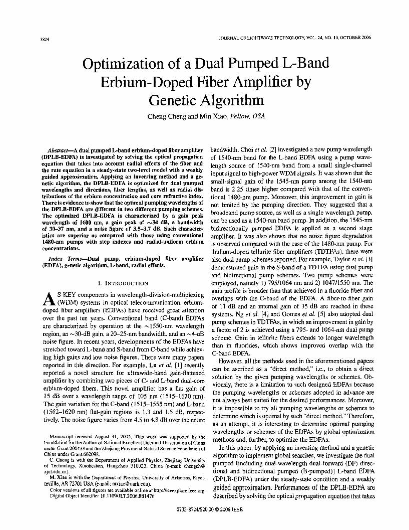


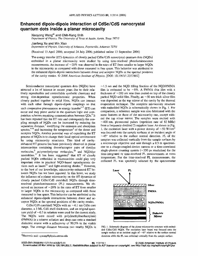


![Sangeetha [Ferroelectric Memory]](https://static.documents.pub/doc/80x56/55cf8f91550346703b9d9665/sangeetha-ferroelectric-memory.jpg)


