HIGHLIGHTSThis section of the manual contains the following major topics:
21.1 Overview ...................................................................................................................... 21-221.2 I2C Bus Characteristics................................................................................................ 21-421.3 Control and Status Registers ....................................................................................... 21-821.4 Enabling I2C Operation .............................................................................................. 21-1321.5 Communicating as a Master in a Single-Master Environment ................................... 21-1521.6 Communicating as a Master in a Multi-Master Environment ..................................... 21-2921.7 Communicating as a Slave ........................................................................................ 21-3221.8 Connection Considerations for I2C Bus ..................................................................... 21-4721.9 Module Operation During PWRSAV Instruction......................................................... 21-4921.10 Effects of a Reset....................................................................................................... 21-4921.11 Register Maps............................................................................................................ 21-5021.12 Design Tips ................................................................................................................ 21-5121.13 Related Application Notes.......................................................................................... 21-5221.14 Revision History ......................................................................................................... 21-53
21.1 OverviewThe Inter-Integrated Circuit™ (I2C™) module is a serial interface useful for communicating withother peripheral or microcontroller devices. These peripheral devices may be serial EEPROMs,display drivers, A/D converters and so on.
The I2C module can operate in any of the following I2C systems:
• Where the dsPIC30F acts as a Slave Device• Where the dsPIC30F acts as a Master Device in a Single Master System
(Slave may also be active)• Where the dsPIC30F acts as a Master/Slave Device in a Multi-Master System
(Bus collision detection and arbitration available)
The I2C module contains independent I2C master logic and I2C slave logic, each generatinginterrupts based on their events. In multi-master systems, the software is simply partitioned intomaster controller and slave controller.
When the I2C master logic is active, the slave logic remains active also, detecting the state of thebus and potentially receiving messages from itself in a single master system or from othermasters in a multi-master system. No messages are lost during multi-master bus arbitration.
In a multi-master system, bus collision conflicts with other masters in the system are detectedand the module provides a method to terminate then restart the message.
The I2C module contains a baud rate generator. The I2C baud rate generator does not consumeother timer resources in the device.
21.1.1 Module Features
• Independent Master and Slave logic• Multi-Master support. No messages lost in arbitration• Detects 7-bit and 10-bit device addresses• Detects general call addresses as defined in the I2C protocol• Bus Repeater mode. Accept all messages as a slave regardless of the address• Automatic SCL clock stretching provides delays for the processor to respond to a slave
data request• Supports 100 kHz and 400 kHz bus specifications
Figure 21-1 illustrates the I2C module block diagram.
21.2 I2C Bus CharacteristicsThe I2C bus is a two-wire serial interface. Figure 21-2 is a schematic of a typical I2C connectionbetween the dsPIC30F device and a 24LC256 I2C serial EEPROM.
The I2C interface employs a comprehensive protocol to ensure reliable transmission andreception of data. When communicating, one device is the “master” which initiates transfer onthe bus and generates the clock signals to permit that transfer, while the other device(s) acts asthe “slave” responding to the transfer. The clock line, “SCL”, is output from the master and inputto the slave, although occasionally the slave drives the SCL line. The data line, “SDA”, may beoutput and input from both the master and slave.
Because the SDA and SCL lines are bidirectional, the output stages of the devices driving theSDA and SCL lines must have an open drain in order to perform the wired-AND function of thebus. External pull-up resistors are used to ensure a high level when no device is pulling the linedown.
In the I2C interface protocol, each device has an address. When a master wants to initiate a datatransfer, it first transmits the address of the device that it wants to “talk” to. All devices “listen” tosee if this is their address. Within this address, bit ‘0’ specifies if the master wants to read fromor write to the slave device. The master and slave are always in opposite modes(transmitter/receiver) of operation during a data transfer. That is, they can be thought of asoperating in either of these two relations:
• Master-transmitter and Slave-receiver• Slave-transmitter and Master-receiver
In both cases, the master originates the SCL clock signal.
• Data transfer may be initiated only when the bus is not busy.• During data transfer, the data line must remain stable whenever the SCL clock line is HIGH.
Changes in the data line while the SCL clock line is HIGH will be interpreted as a Start or Stop condition.
Accordingly, the following bus conditions are defined in Figure 21-3.
21.2.1.1 Start Data Transfer (S)
After a bus Idle state, a HIGH-to-LOW transition of the SDA line while the clock (SCL) is HIGHdetermines a Start condition. All data transfers must be preceded by a Start condition.
21.2.1.2 Stop Data Transfer (P)
A LOW-to-HIGH transition of the SDA line while the clock (SCL) is HIGH determines a Stopcondition. All data transfers must end with a Stop condition.
21.2.1.3 Repeated Start (R)
After a WAIT state, a HIGH-to-LOW transition of the SDA line while the clock (SCL) is HIGHdetermines a Repeated Start condition. Repeated Starts allow a master to change bus directionwithout relinquishing control of the bus.
21.2.1.4 Data Valid (D)
The state of the SDA line represents valid data when, after a Start condition, the SDA line isstable for the duration of the HIGH period of the clock signal. There is one bit of data per SCLclock.
21.2.1.5 Acknowledge (A) or Not-Acknowledge (N)
All data byte transmissions must be Acknowledged (ACK) or Not-Acknowledged (NACK) by thereceiver. The receiver will pull the SDA line low for an ACK or release the SDA line for a NACK.The Acknowledge is a one-bit period, using one SCL clock.
21.2.1.6 WAIT/Data Invalid (Q)
The data on the line must be changed during the LOW period of the clock signal. Devices mayalso stretch the clock low time, by asserting a low on SCL line, causing a WAIT on the bus.
21.2.1.7 Bus Idle (I)
Both data and clock lines remain HIGH at those times after a Stop condition and before a Startcondition.
A typical I2C message is shown in Figure 21-4. In this example, the message will read a specifiedbyte from a 24LC256 I2C serial EEPROM. The dsPIC30F device will act as the master and the24LC256 device will act as the slave.
Figure 21-4 indicates the data as driven by the master device and the data as driven by the slavedevice, remembering that the combined SDA line is a wired-AND of the master and slave data.The master device controls and sequences the protocol. The slave device will only drive the busat specifically determined times.
Figure 21-4: A Typical I2C™ Message: Read of Serial EEPROM (Random Address Mode)
21.2.2.1 Start Message
Each message is initiated with a “Start” condition and terminated with a “Stop” condition. Thenumber of the data bytes transferred between the Start and Stop conditions is determined by themaster device. As defined by the system protocol, the bytes of the message may have specialmeaning such as “device address byte” or “data byte”.
21.2.2.2 Address Slave
In the Figure 21-4, the first byte is the device address byte that must be the first part of any I2Cmessage. It contains a device address and a R/W bit. Refer to “Section 26. Appendix” foradditional information on Address Byte formats. Note that R/W = 0 for this first address byte,indicating that the master will be a transmitter and the slave will be a receiver.
21.2.2.3 Slave Acknowledge
The receiving device is obliged to generate an Acknowledge signal, “ACK”, after the reception ofeach byte. The master device must generate an extra SCL clock, which is associated with thisAcknowledge bit.
21.2.2.4 Master Transmit
The next 2 bytes, sent by the master to the slave, are data bytes containing the location of therequested EEPROM data byte. The slave must Acknowledge each of the data bytes.
21.2.2.5 Repeated Start
At this point, the slave EEPROM has the address information necessary to return the requesteddata byte to the master. However, the R/W bit from the first device address byte specified mastertransmission and slave reception. The bus must be turned in the other direction for the slave tosend data to the master.
To do this function without ending the message, the master sends a “Repeated Start”. TheRepeated Start is followed with a device address byte containing the same device address asbefore and with the R/W = 1 to indicate slave transmission and master reception.
21.3 Control and Status RegistersThe I2C module has six user-accessible registers for I2C operation. The registers are accessiblein either Byte or Word mode. The registers are shown in Figure 21-5 and listed below:
• Control Register (I2CCON): This register allows control of the I2C operation.• Status Register (I2CSTAT): This register contains status flags indicating the module state
during I2C operation.• Receive Buffer Register (I2CRCV): This is the buffer register from which data bytes can be
read. The I2CRCV register is a read only register.• Transmit Register (I2CTRN): This is the transmit register; bytes are written to this register
during a transmit operation. The I2CTRN register is a read/write register.• Address Register (I2CADD): The I2CADD register holds the slave device address. • Baud Rate Generator Reload Register (I2CBRG): Holds the baud rate generator reload
value for the I2C module baud rate generator.
Figure 21-5: I2C™ Programmer’s Model
Register 21-1 and Register 21-2 define the I2C module Control and Status registers, I2CCONand I2CSTAT.
The I2CTRN is the register to which transmit data is written. This register is used when themodule operates as a master transmitting data to the slave or as a slave sending reply data tothe master. As the message progresses, the I2CTRN register shifts out the individual bits.Because of this, the I2CTRN may not be written to unless the bus is Idle. The I2CTRN may bereloaded while the current data is transmitting.
Data being received by either the master or the slave is shifted into a non-accessible Shiftregister called I2CRSR. When a complete byte is received, the byte transfers to the I2CRCVregister. In receive operations, the I2CRSR and I2CRCV create a double-buffered receiver. Thisallows reception of the next byte to begin before reading the current byte of received data.
If the module receives another complete byte before the software reads the previous byte fromthe I2CRCV register, a receiver overflow occurs and sets the I2COV (I2CCON<6>). The byte inthe I2CRSR is lost.
The I2CADD register holds the slave device address. In 10-bit mode, all bits are relevant. In7-bit addressing mode, only I2CADD<6:0> are relevant. The A10M (I2CCON<10>) specifies theexpected mode of the slave address.
bit 15 I2CEN: I2C Enable bit 1 = Enables the I2C module and configures the SDA and SCL pins as serial port pins0 = Disables I2C module. All I2C pins are controlled by port functions
bit 14 Unimplemented: Read as ‘0’bit 13 I2CSIDL: Stop in Idle Mode bit
1 = Discontinue module operation when device enters an Idle mode0 = Continue module operation in Idle mode
bit 12 SCLREL: SCL Release Control bit (when operating as I2C Slave)1 = Release SCL clock0 = Hold SCL clock low (clock stretch)If STREN = 1: Bit is R/W (i.e., software may write ‘0’ to initiate stretch and write ‘1’ to release clock)Hardware clear at beginning of slave transmission.Hardware clear at end of slave reception.If STREN = 0:Bit is R/S (i.e., software may only write ‘1’ to release clock)Hardware clear at beginning of slave transmission.
bit 11 IPMIEN: Intelligent Platform Management Interface (IPMI) Enable bit(1)
1 = Enable IPMI Support mode. All addresses Acknowledged0 = IPMI mode not enabled
bit 10 A10M: 10-Bit Slave Address bit1 = I2CADD is a 10-bit slave address0 = I2CADD is a 7-bit slave address
bit 9 DISSLW: Disable Slew Rate Control bit1 = Slew rate control disabled0 = Slew rate control enabled
bit 7 GCEN: General Call Enable bit (when operating as I2C slave)1 = Enable interrupt when a general call address is received in the I2CRSR
(module is enabled for reception)0 = General call address disabled
bit 6 STREN: SCL Clock Stretch Enable bit (when operating as I2C slave)Used in conjunction with SCLREL bit.1 = Enable software or receive clock stretching0 = Disable software or receive clock stretching
bit 5 ACKDT: Acknowledge Data bit (When operating as I2C Master. Applicable during master receive.)Value that will be transmitted when the software initiates an Acknowledge sequence.1 = Send NACK during acknowledge0 = Send ACK during acknowledge
Note 1: The IPMIEN bit should not be set when operating as a master.
Register 21-1: I2CCON: I2C™ Control Register (Continued)
bit 4 ACKEN: Acknowledge Sequence Enable bit(When operating as I2C master. Applicable during master receive.)1 = Initiate Acknowledge sequence on SDA and SCL pins, and transmit ACKDT data bit
Hardware clear at end of master Acknowledge sequence.0 = Acknowledge sequence not in progress
bit 3 RCEN: Receive Enable bit (when operating as I2C master)1 = Enables Receive mode for I2C
Hardware clear at end eighth bit of master receive data byte.0 = Receive sequence not in progress
bit 2 PEN: Stop Condition Enable bit (when operating as I2C master)1 = Initiate Stop condition on SDA and SCL pins
Hardware clear at end of master Stop sequence.0 = Stop condition not in progress
bit 1 RSEN: Repeated Start Condition Enable bit (when operating as I2C master)1 = Initiate Repeated Start condition on SDA and SCL pins
Hardware clear at end of master Repeated Start sequence.0 = Repeated Start condition not in progress
bit 0 SEN: Start Condition Enable bit (when operating as I2C master)1 = Initiate Start condition on SDA and SCL pins
Hardware clear at end of master Start sequence.0 = Start condition not in progress
Note 1: The IPMIEN bit should not be set when operating as a master.
Legend:R = Readable C = Clearable bit U = Unimplemented bit, read as ‘0’W = Writable HS = Set by Hardware S = Settable bitHC = Cleared by Hardware ‘0’ = Bit cleared at POR x = Bit is unknown at POR‘1’ = Bit is set at POR
Register 21-2: I2CSTAT: I2C™ Status RegisterUpper Byte:
R-0HS, HC
R-0HS, HC
U-0 U-0 U-0 R/C-0HS
R-0HS, HC
R-0HS, HC
ACKSTAT TRSTAT — — — BCL GCSTAT ADD10bit 15 bit 8
Lower Byte:R/C-0
HSR/W-0
HSR-0
HS, HCR-0
HS, HCR-0
HS, HCR-0
HS, HCR-0
HS, HCR-0
HS, HC
IWCOL I2COV D/A P S R/W RBF TBFbit 7 bit 0
bit 15 ACKSTAT: Acknowledge Status bit (When operating as I2C master. Applicable to master transmit operation.)1 = NACK received from slave0 = ACK received from slaveHardware set or clear at end of slave Acknowledge.
bit 14 TRSTAT: Transmit Status bit (When operating as I2C master. Applicable to master transmit operation.)1 = Master transmit is in progress (8 bits + ACK)0 = Master transmit is not in progressHardware set at beginning of master transmission.Hardware clear at end of slave Acknowledge.
bit 13-11 Unimplemented: Read as ‘0’bit 10 BCL: Master Bus Collision Detect bit
1 = A bus collision has been detected during a master operation0 = No collisionHardware set at detection of bus collision.
bit 9 GCSTAT: General Call Status bit1 = General call address was received0 = General call address was not receivedHardware set when address matches general call address.Hardware clear at Stop detection.
bit 8 ADD10: 10-Bit Address Status bit1 = 10-bit address was matched0 = 10-bit address was not matchedHardware set at match of 2nd byte of matched 10-bit address.Hardware clear at Stop detection.
bit 7 IWCOL: Write Collision Detect bit1 = An attempt to write the I2CTRN register failed because the I2C module is busy 0 = No collisionHardware set at occurrence of write to I2CTRN while busy (cleared by software).
bit 6 I2COV: Receive Overflow Flag bit1 = A byte was received while the I2CRCV register is still holding the previous byte0 = No overflowHardware set at attempt to transfer I2CRSR to I2CRCV (cleared by software).
bit 5 D/A: Data/Address bit (when operating as I2C slave)1 = Indicates that the last byte received was data0 = Indicates that the last byte received was a device addressHardware clear at device address match; hardware set by reception of slave byte or is set after thetransmission is complete and the TBF flag is cleared.
Register 21-2: I2CSTAT: I2C™ Status Register (Continued)
bit 4 P: Stop bit 1 = Indicates that a Stop bit has been detected last0 = Stop bit was not detected lastHardware set or clear when Start, Repeated Start or Stop detected.
bit 3 S: Start bit 1 = Indicates that a Start (or Repeated Start) bit has been detected last0 = Start bit was not detected lastHardware set or clear when Start, Repeated Start or Stop detected.
bit 2 R/W: Read/Write bit Information (when operating as I2C slave)1 = Read - indicates data transfer is output from slave0 = Write - indicates data transfer is input to slaveHardware set or clear after reception of I2C device address byte.
bit 1 RBF: Receive Buffer Full Status bit 1 = Receive complete, I2CRCV is full0 = Receive not complete, I2CRCV is emptyHardware set when I2CRCV written with received byte.Hardware clear when software reads I2CRCV.
bit 0 TBF: Transmit Buffer Full Status bit1 = Transmit in progress, I2CTRN is full0 = Transmit complete, I2CTRN is emptyHardware set when software writes I2CTRN.Hardware clear at completion of data transmission.
Legend:R = Readable W = Writable C = Clearable bitHC = Cleared by Hardware HS = Set by Hardware U = Unimplemented bit, read as ‘0’‘1’ = Bit is set at POR ‘0’ = Bit cleared at POR x = Bit is unknown at POR
The module is enabled by setting the I2CEN (I2CCON<15>) bit.
The I2C module fully implements all master and slave functions. When the module is enabled,the master and slave functions are active simultaneously and will respond according to thesoftware or the bus events.
When initially enabled, the module will release SDA and SCL pins, putting the bus into the Idlestate. The master functions will remain in the Idle state unless software sets a control bit to initiatea master event. The slave functions will begin to monitor the bus. If the slave logic detects a Startevent and a valid address on the bus, the slave logic will begin a slave transaction.
21.4.1 Enabling I2C I/O
Two pins are used for bus operation. These are the SCL pin, which is the clock, and the SDA pin,which is the data. When the module is enabled, assuming no other module with higher priorityhas control, the module will assume control of the SDA and SCL pins. The module software neednot be concerned with the state of the port I/O of the pins, the module overrides the port stateand direction. At initialization, the pins are tri-state (released).
21.4.2 I2C Interrupts
The I2C module generates two interrupts. One interrupt is assigned to master events and theother interrupt is assigned to slave events. These interrupts will set a corresponding interrupt flagbit and will interrupt the software process if the corresponding interrupt enable bit is set and thecorresponding interrupt priority is high enough.
The master interrupt is called MI2CIF and is activated on completion of a master message event.
The following events generate the MI2CIF interrupt:
• Start condition• Stop condition• Data transfer byte transmitted/received• Acknowledge transmit• Repeated Start• Detection of a bus collision event
The slave interrupt is called SI2CIF and is activated on detection of a message directed to theslave.
• Detection of a valid device address (including general call)• Transmission of data byte• Reception of data byte
21.4.3 Setting Baud Rate when Operating as a Bus Master
When operating as an I2C master, the module must generate the system SCL clock. Generally,I2C system clocks are specified to be either 100 kHz, 400 kHz or 1 MHz. The system clock rateis specified as the minimum SCL low time plus the minimum SCL high time. In most cases, thatis defined by 2 TBRG intervals.
The reload value for the baud rate generator is the I2CBRG register, as shown in Figure 21-6.When the baud rate generator is loaded with this value, the generator counts down to ‘0’ andstops until another reload has taken place. The generator count is decremented twice per instruc-tion cycle (TCY). The baud rate generator is reloaded automatically on baud rate restart. Forexample, if clock synchronization is taking place, the baud rate generator will be reloaded whenthe SCL pin is sampled high.
To compute the baud rate generator reload value, use the following equation.
21.5 Communicating as a Master in a Single-Master Environment
Typical operation of the I2C module in a system is using the I2C to communicate with an I2Cperipheral, such as an I2C serial memory. In an I2C system, the master controls the sequence ofall data communication on the bus. In this example, the dsPIC30F and its I2C module have therole of the single master in the system. As the single master, it is responsible for generating theSCL clock and controlling the message protocol.
In the I2C module, the module controls individual portions of the I2C message protocol, however,sequencing of the components of the protocol to construct a complete message is a softwaretask.
For example, a typical operation in a single master environment may be to read a byte from anI2C serial EEPROM. This example message is depicted in Figure 21-7.
To accomplish this message, the software will sequence through the following steps:
1. Assert a Start condition on SDA and SCL.2. Send the I2C device address byte to the slave with a write indication.3. Wait for and verify an Acknowledge from the slave.4. Send the serial memory address high byte to the slave.5. Wait for and verify an Acknowledge from the slave.6. Send the serial memory address low byte to the slave.7. Wait for and verify an Acknowledge from the slave.8. Assert a Repeated Start condition on SDA and SCL.9. Send the device address byte to the slave with a read indication.10. Wait for and verify an Acknowledge from the slave.11. Enable master reception to receive serial memory data.12. Generate an ACK or NACK condition at the end of a received byte of data.13. Generate a Stop condition on SDA and SCL.
Figure 21-7: A Typical I2C™ Message: Read of Serial EEPROM (Random Address Mode)
The I2C module supports Master mode communication with the inclusion of Start and Stopgenerators, data byte transmission, data byte reception, Acknowledge generator and a baudrate generator.
Generally, the software will write to a control register to start a particular step, then wait for aninterrupt or poll status to wait for completion.
Subsequent sub-sections detail each of these operations.
Note: The IPMIEN (I2CxCON<11>) bit should not be set when operating as a master.
Bus
MasterSDA
ACK
NAC
ACK
ACK
ACK
STOP
START
AddressByte
EE ADDRHigh Byte
EE ADDRLow Byte
AddressByte
DataByte
START
S 1 0 1 0 A A A 02 1 0 R 1 0 1 0 A A A 12 1 0 P
K
SlaveSDA
Activity
N
AAAA
ER
R/
W
R/
W
Output
Output
IDLE
IDLE
Note: The I2C module does not allow queueing of events. For instance, the software is notallowed to initiate a Start condition and immediately write the I2CxTRN register toinitiate transmission before the Start condition is complete. In this case, theI2CxTRN register will not be written to and the IWCOL status bit will be set,indicating that this write to the I2CxTRN register did not occur.
To initiate a Start event, the software sets the Start enable bit, SEN (I2CCON<0>). Prior tosetting the Start bit, the software can check the P (I2CSTAT<4>) status bit to ensure that the busis in an Idle state.
Figure 21-8 shows the timing of the Start condition.
• Slave logic detects the Start condition, sets the S bit (I2CSTAT<3>) and clears the P bit (I2CSTAT<4>).
• SEN bit is automatically cleared at completion of the Start condition.• MI2CIF interrupt generated at completion of the Start condition.• After Start condition, the SDA line and SCL line are left low (Q state).
21.5.1.1 IWCOL Status Flag
If the software writes the I2CTRN when a Start sequence is in progress, then IWCOL is set andthe contents of the transmit buffer are ignored.
Figure 21-8: Master Start Timing Diagram
Note: Since queueing of events is not allowed, writing to the lower 5 bits of I2CCON isdisabled until the Start condition is complete.
SCL (Master)
SDA (Master)
S
SEN
MI2CIF Interrupt
TBRG
1 2 3 4
- Writing SEN = 1 initiates a master Start event. 1
Transmission of a data byte, a 7-bit device address byte or the second byte of a 10-bit address,is accomplished by simply writing the appropriate value to the I2CTRN register. Loading thisregister will start the following process:
• The software loads the I2CTRN with the data byte to transmit.• Writing I2CTRN sets the buffer full flag bit, TBF (I2CSTAT<0>).• The data byte is shifted out the SDA pin until all 8 bits are transmitted. Each bit of
address/data will be shifted out onto the SDA pin after the falling edge of SCL.• On the ninth SCL clock, the module shifts in the ACK bit from the slave device and writes its
value into the ACKSTAT bit (I2CCON<15>).• The module generates the MI2CIF interrupt at the end of the ninth SCL clock cycle.
Note that the module does not generate or validate the data bytes. The contents and usage ofthe byte is dependant on the state of the message protocol maintained by the software.
21.5.2.1 Sending a 7-bit Address to the Slave
Sending a 7-bit device address involves sending 1 byte to the slave. A 7-bit address byte mustcontain the 7 bits of I2C device address and a R/W bit that defines if the message will be a writeto the slave (master transmission and slave receiver) or a read from the slave (slave transmissionand master receiver).
21.5.2.2 Sending a 10-bit Address to the Slave
Sending a 10-bit device address involves sending 2 bytes to the slave. The first byte contains 5bits of I2C device address reserved for 10-bit Addressing modes and 2 bits of the 10-bit address.Because the next byte, which contains the remaining 8 bits of the 10-bit address must bereceived by the slave, the R/W bit in the first byte must be ‘0’, indicating master transmission andslave reception. If the message data is also directed toward the slave, the master can continuesending the data. However, if the master expects a reply from the slave, a Repeated Startsequence with the R/W bit at ‘1’ will change the R/W state of the message to a read of the slave.
21.5.2.3 Receiving Acknowledge from the Slave
On the falling edge of the eighth SCL clock, the TBF bit is cleared and the master will de-assertthe SDA pin allowing the slave to respond with an Acknowledge. The master will then generatea ninth SCL clock.
This allows the slave device being addressed to respond with an ACK bit during the ninthbit time if an address match occurs, or if data was received properly. A slave sends anAcknowledge when it has recognized its device address (including a general call), or when theslave has properly received its data.
The status of ACK is written into the Acknowledge status bit, ACKSTAT (I2CSTAT<15>), on thefalling edge of the ninth SCL clock. After the ninth SCL clock, the module generates the MI2CIFinterrupt and enters an Idle state until the next data byte is loaded into I2CTRN.
21.5.2.4 ACKSTAT Status Flag
The ACKSTAT bit (I2CCON<15>) is cleared when the slave has sent an Acknowledge(ACK = 0), and is set when the slave does not Acknowledge (ACK = 1).
Note: In 7-bit addressing mode, each node using the I2C protocol should be configuredwith a unique address that is stored in the I2CxADD register.
Note: In 10-bit addressing mode, each node using the I2C protocol should be configuredwith a unique address that is stored in the I2CxADD register.
When transmitting, the TBF bit (I2CSTAT<0>) is set when the CPU writes to I2CTRN and iscleared when all 8 bits are shifted out.
21.5.2.6 IWCOL Status Flag
If the software writes the I2CTRN when a transmit is already in progress (i.e., the module is stillshifting out a data byte), then IWCOL is set and the contents of the buffer are ignored. IWCOLmust be cleared in software.
Figure 21-9: Master Transmission Timing Diagram
Note: Since queueing of events is not allowed, writing to the lower 5 bits of I2CCON isdisabled until the transmit condition is complete.
D7 D6 D5 D4 D3 D2 D1 D0
SCL (Master)
SCL (Slave)
SDA (Master)
SDA (Slave)
TBF
I2CTRN
MI2CIF Interrupt
TBRG TBRG
5 6 7 81 2 3 4
- Writing the I2CTRN register will start a master transmission event. TBF bit is set.1
- Baud Rate Generator starts. The MSB of the I2CTRN drives SDA. SCL remains low. TRSTAT bit is set.2
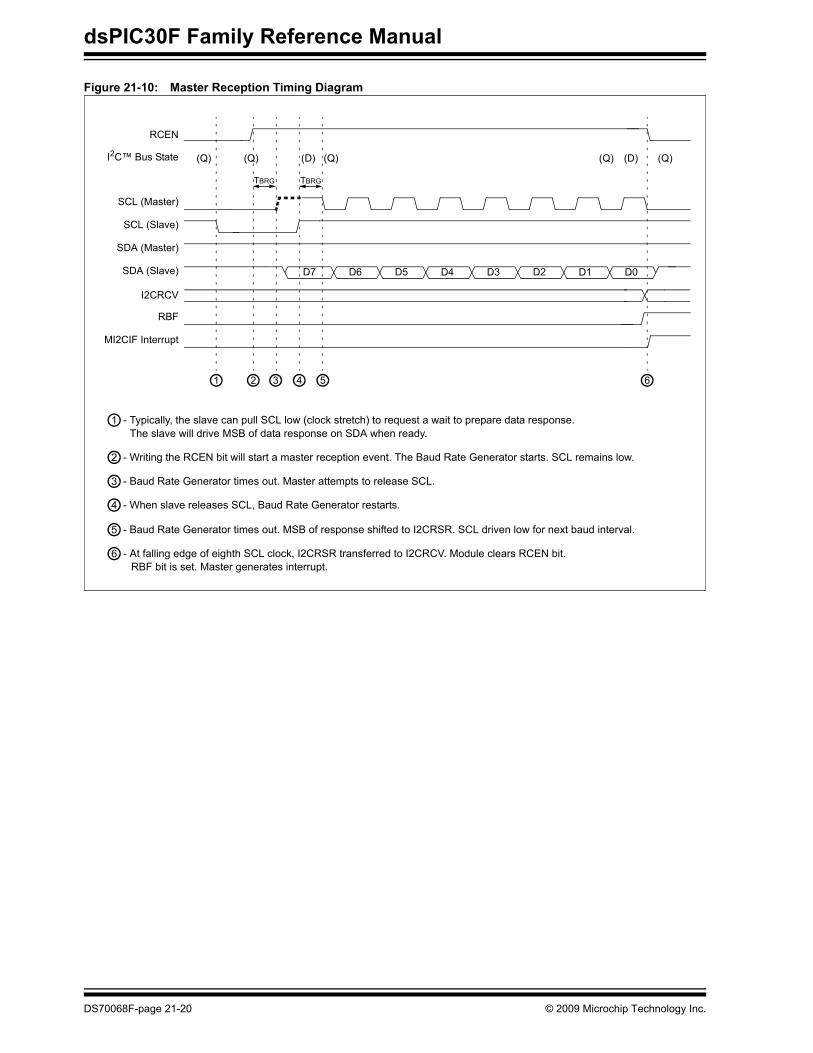
Setting the receive enable bit, RCEN (I2CCON<3>), enables the master to receive data from aslave device.
The master logic begins to generate clocks and before each falling edge of the SCL, SDA line issampled and data is shifted into the I2CRSR.
After the falling edge of the eighth SCL clock:
• The RCEN bit is automatically cleared.• The contents of the I2CRSR transfer into the I2CRCV.• The RBF flag bit is set.• The module generates the MI2CIF interrupt.
When the CPU reads the buffer, the RBF flag bit is automatically cleared. The software canprocess the data and then do an Acknowledge sequence.
21.5.3.1 RBF Status Flag
When receiving data, the RBF bit is set when a device address or data byte is loaded intoI2CRCV from I2CRSR. It is cleared when software reads the I2CRCV register.
21.5.3.2 I2COV Status Flag
If another byte is received in the I2CRSR while the RBF bit remains set and the previous byteremains in the I2CRCV register, the I2COV bit is set and the data in the I2CRSR is lost.
Leaving I2COV set does not inhibit further reception. If RBF is cleared by reading the I2CRCV,and the I2CRSR receives another byte, that byte will be transferred to the I2CRCV.
21.5.3.3 IWCOL Status Flag
If the software writes the I2CTRN when a receive is already in progress (i.e., I2CRSR is stillshifting in a data byte), then the IWCOL bit is set and the contents of the buffer are ignored.
Note: The lower 5 bits of I2CCON must be ‘0’ before attempting to set the RCEN bit. Thisensures the master logic is inactive.
Note: Since queueing of events is not allowed, writing to the lower 5 bits of I2CCON isdisabled until the data reception condition is complete.
- Writing the RCEN bit will start a master reception event. The Baud Rate Generator starts. SCL remains low.2
- Baud Rate Generator times out. Master attempts to release SCL. 3
- When slave releases SCL, Baud Rate Generator restarts.4
- Baud Rate Generator times out. MSB of response shifted to I2CRSR. SCL driven low for next baud interval. 5
- At falling edge of eighth SCL clock, I2CRSR transferred to I2CRCV. Module clears RCEN bit. 6
TBRG
RCEN
(Q) (D) (Q) (Q)(D)(Q)
I2CRCV
RBF bit is set. Master generates interrupt.
(Q)
1
- Typically, the slave can pull SCL low (clock stretch) to request a wait to prepare data response. 1The slave will drive MSB of data response on SDA when ready.
Setting the Repeated Start sequence enable bit, RSEN (I2CCON<1>), enables generation of amaster Repeated Start sequence (see Figure 21-14).
To generate a Repeated Start condition, software sets the RSEN bit (I2CCON<1>). The moduleasserts the SCL pin low. When the module samples the SCL pin low, the module releases theSDA pin for one baud rate generator count (TBRG). When the baud rate generator times out, ifthe module samples SDA high, the module de-asserts the SCL pin. When the module samplesSCL pin high, the baud rate generator reloads and begins counting. SDA and SCL must besampled high for one TBRG. This action is then followed by assertion of the SDA pin low for oneTBRG while SCL is high.
The following is the Repeated Start sequence:
• The slave detects the Start condition, sets the S bit (I2CSTAT<3>) and clears the P bit (I2CSTAT<4>)
• The RSEN bit is automatically cleared• The module generates the MI2CIF interrupt
21.5.6.1 IWCOL Status Flag
If the software writes the I2CTRN when a Repeated Start sequence is in progress, then IWCOLis set and the contents of the buffer are ignored.
As described at the beginning of 21.5 “Communicating as a Master in a Single-Master Envi-ronment”, the software is responsible for constructing messages with the correct message pro-tocol. The module controls individual portions of the I2C message protocol, however, sequencingof the components of the protocol to construct a complete message is a software task.
The software can use polling or interrupt methods while using the module. The examples shownuse interrupts.
The software can use the SEN, RSEN, PEN, RCEN and ACKEN bits (Least Significant 5 bits ofthe I2CCON register) and the TRSTAT bit as a “state” flag when progressing through a message.For example, Table 21-2 shows some example state numbers associated with bus states.
Table 21-2: Master Message Protocol States
The software will begin a message by issuing a Start command. The software will record the statenumber corresponding to Start.
As each event completes and generates an interrupt, the interrupt handler may check the statenumber. So, for a Start state, the interrupt handler will confirm execution of the Start sequenceand then start a master transmission event to send the I2C device address, changing the statenumber to correspond to master transmission.
On the next interrupt, the interrupt handler will again check the state, determining that a mastertransmission just completed. The interrupt handler will confirm successful transmission of thedata, then move on to the next event, depending on the contents of the message.
In this manner, on each interrupt, the interrupt handler will progress through the messageprotocol until the complete message is sent.
Figure 21-15 provides a more detailed examination of the same message sequence ofFigure 21-7.
Figure 21-16 shows some simple examples of messages using 7-bit addressing format.
Figure 21-17 shows an example of a 10-bit address format message sending data to a slave.
Figure 21-18 shows an example of a 10-bit address format message receiving data from a slave.
21.6 Communicating as a Master in a Multi-Master Environment
The I2C protocol allows for more than one master to be attached to a system bus. Remember-ing that a master can initiate message transactions and generate clocks for the bus, theprotocol has methods to account for situations where more than one master is attempting tocontrol the bus. Clock synchronization ensures that multiple nodes can synchronize their SCLclocks to result in one common clock on the SCL line. Bus arbitration ensures that if more thanone node attempts a message transaction, one and only one node will be successful incompleting the message. The other nodes will lose bus arbitration and be left with a buscollision.
21.6.1 Multi-Master Operation
The master module has no special settings to enable multi-master operation. The moduleperforms clock synchronization and bus arbitration at all times. If the module is used in a singlemaster environment, clock synchronization will only occur between the master and slaves andbus arbitration will not occur.
21.6.2 Master Clock Synchronization
In a multi-master system, different masters may have different baud rates. Clock synchronizationwill ensure that when these masters are attempting to arbitrate the bus, their clocks will becoordinated.
Clock synchronization occurs when the master de-asserts the SCL pin (SCL intended to floathigh). When the SCL pin is released, the Baud Rate Generator (BRG) is suspended fromcounting until the SCL pin is actually sampled high. When the SCL pin is sampled high, the baudrate generator is reloaded with the contents of I2CBRG<8:0> and begins counting. This ensuresthat the SCL high time will always be at least one BRG rollover count in the event that the clockis held low by an external device, as shown in Figure 21-19.
Figure 21-19: Baud Rate Generator Timing with Clock Synchronization
Note: The IPMIEN (I2CxCON<11>) bit should not be set when operating as a master.
SCL (Slave)
- The baud counter decrements twice per TCY. On rollover, the master SCL will transition.1
1
000 003001002003000
SCL (Master)
001002003000Baud Counter
SDA (Master)
3 4 6
- The slave has pulled SCL low to initiate a wait.2
- At what would be the master baud counter rollover, detecting SCL low holds counter.3
- Logic samples SCL once per TCY. Logic detects SCL high.4
2
- The baud counter rollover occurs on next cycle.5
5
- On next rollover, the master SCL will transition.6
Bus arbitration supports multi-master system operation.
The wired-and nature of the SDA line permits arbitration. Arbitration takes place when the firstmaster outputs a ‘1’ on SDA by letting SDA float high and, simultaneously, the second masteroutputs a ‘0’ on SDA by pulling SDA low. The SDA signal will go low. In this case, the secondmaster has won bus arbitration. The first master has lost bus arbitration and thus has a buscollision.
For the first master, the expected data on SDA is a ‘1’ yet the data sampled on SDA is a ‘0’. Thisis the definition of a bus collision.
The first master will set the bus collision bit, BCL (I2CSTAT<10>), and generate a masterinterrupt. The master module will reset the I2C port to its Idle state.
In multi-master operation, the SDA line must be monitored for arbitration to see if the signallevel is the expected output level. This check is performed by the master module, with the resultplaced in the BCL bit.
The states where arbitration can be lost are:
• A Start condition • A Repeated Start condition• Address, Data or Acknowledge bit• A Stop condition
21.6.4 Detecting Bus Collisions and Resending Messages
When a bus collision occurs, the I2C module sets the BCL bit and generates a master interrupt.If bus collision occurs during a byte transmission, the transmission is halted, the TBF flag iscleared and the SDA and SCL pins are de-asserted. If bus collision occurs during a Start,Repeated Start, Stop or Acknowledge condition, the condition is aborted, the respective controlbits in the I2CCON register are cleared and the SDA and SCL lines are de-asserted.
The software is expecting an interrupt at the completion of the master event. The software cancheck the BCL bit to determine if the master event completed successfully or if a collisionoccurred. If a collision occurs, the software must abort sending the rest of the pending messageand prepare to resend the entire message sequence beginning with Start condition, after thebus returns to an Idle state. The software can monitor the S and P bits to wait for an Idle bus.When the software services the master Interrupt Service Routine (ISR) and the I2C bus is free,the software can resume communication by asserting a Start condition.
Before issuing a Start command, the software should verify an Idle state of the bus using the Sand P status bits. Two masters may attempt to initiate a message at a similar point in time.Typically, the masters will synchronize clocks and continue arbitration into the message until oneloses arbitration. However, certain conditions can cause a bus collision to occur during a Start.In this case, the master that loses arbitration during the Start bit generates a bus collisioninterrupt.
21.6.6 Bus Collision During a Repeated Start Condition
Should two masters not collide throughout an address byte, a bus collision may occur when onemaster attempts to assert a Repeated Start while another transmits data. In this case, themaster generating the Repeated Start will lose arbitration and generate a bus collision interrupt.
21.6.7 Bus Collision During Message Bit Transmission
The most typical case of data collision occurs while the master is attempting to transmit thedevice address byte, a data byte or an Acknowledge bit.
If the software is properly checking the bus state, it is unlikely that a bus collision will occur on aStart condition. However, because another master can, at a very similar time, check the bus andinitiate its own Start condition, it is likely that SDA arbitration will occur and synchronize thestarts of two masters. In this condition, both masters will begin and continue to transmit theirmessages until one master loses arbitration on a message bit. Remember that SCL clocksynchronization will keep the two masters synchronized until one loses arbitration.
Figure 21-20 shows an example of message bit arbitration.
Figure 21-20: Bus Collision During Message Bit Transmission
21.6.8 Bus Collision During a Stop Condition
If the master software loses track of the state of the I2C bus, there are conditions which cause abus collision during a Stop condition. In this case, the master generating the Stop condition willlose arbitration and generate a bus collision interrupt.
SCL (Master)
SDA (Master)
TBF
TBRG
1 2 3
- Master transmits bit value of ‘1’ in next SCL clock.1TBRG
Module releases SDA.
- Another master on bus transmits bit value of ‘0’ 2in next SCL clock. Another master pulls SDA low.
- Baud Rate Generator times out. Module attempts to verify3
I2C™ Bus State
BCL
(D)
SCL (Bus)
SDA (Bus)
SDA high. Bus collision detected.Module releases SDA and SCL. Module sets BCL bit andclears TBF bit. Master generates interrupt.
21.7 Communicating as a SlaveIn some systems, particularly where multiple processors communicate with each other, thedsPIC30F device may communicate as a slave (see Figure 21-21). When the module isenabled, the slave module is active. The slave may not initiate a message, it can only respondto a message sequence initiated by a master. The master requests a response from a particularslave as defined by the device address byte in the I2C protocol. The slave module replies to themaster at the appropriate times as defined by the protocol.
As with the master module, sequencing the components of the protocol for the reply is asoftware task. However, the slave module detects when the device address matches theaddress specified by the software for that slave.
Figure 21-21: A Typical Slave I2C™ Message: Multiprocessor Command/Status
After a Start condition, the slave module will receive and check the device address. The slavemay specify either a 7-bit address or a 10-bit address. When a device address is matched, themodule will generate an interrupt to notify the software that its device is selected. Based on theR/W bit sent by the master, the slave will either receive or transmit data. If the slave is to receivedata, the slave module automatically generates the Acknowledge (ACK), loads the I2CRCVregister with the received value currently in the I2CRSR register and notifies the softwarethrough an interrupt. If the slave is to transmit data, the software must load the I2CTRN register.
21.7.1 Sampling Receive Data
All incoming bits are sampled with the rising edge of the clock (SCL) line.
21.7.2 Detecting Start and Stop Conditions
The slave module will detect Start and Stop conditions on the bus and indicate that status on theS bit (I2CSTAT<3>) and P bit (I2CSTAT<4>). The Start (S) and Stop (P) bits are cleared when aReset occurs or when the I2C module is disabled. After detection of a Start or Repeated Startevent, the S bit is set and the P bit is cleared. After detection of a Stop event, the P bit is set andthe S bit is clear.
21.7.3 Detecting the Address
Once the module has been enabled, the slave module waits for a Start condition to occur. Aftera Start, depending on the A10M bit (I2CCON<10>), the slave will attempt to detect a 7-bit or10-bit address. The slave module will compare 1 received byte for a 7-bit address or 2 receivedbytes for a 10-bit address. A 7-bit address also contains a R/W bit that specifies the direction ofdata transfer after the address. If R/W = 0, a write is specified and the slave will receive data fromthe master. If R/W = 1, a read is specified and the slave will send data to the master. The 10-bitaddress contains a R/W bit, however by definition, it is always R/W = 0 because the slave mustreceive the second byte of the 10-bit address. In either case, the received address byte istransferred to the I2CRCV register and a dummy read of this register must be performed to clearthe RBF Status bit.
Table 21-3: Slave Addresses Supported by the I2C™ Module
21.7.3.1 7-bit Address and Slave Write
Following the Start condition, the module shifts 8 bits into the I2CRSR register (seeFigure 21-22). The value of register I2CRSR<7:1> is compared to the value of theI2CADD<6:0> register. The device address is compared on the falling edge of the eighth clock(SCL). If the addresses match, the following events occur:
1. An ACK is generated.2. The D/A and R/W bits are cleared.3. The I2C module generates the SI2CIF interrupt on the falling edge of the ninth SCL clock.4. The I2C module will wait for the master to send data.
When a slave read is specified by having R/W = 1 in a 7-bit address byte, the process ofdetecting the device address is similar to that of a slave write (see Figure 21-23). If theaddresses match, the following events occur:
1. An ACK is generated.2. The D/A bit is cleared and the R/W bit is set.3. The module generates the SI2CIF interrupt on the falling edge of the ninth SCL clock.
Since the slave module is expected to reply with data at this point, it is necessary to suspend theoperation of the I2C bus to allow the software to prepare a response. This is done automaticallywhen the module clears the SCLREL bit. With SCLREL low, the slave module will pull down theSCL clock line, causing a wait on the I2C bus. The slave module and the I2C bus will remain inthis state until the software writes the I2CTRN register with the response data and sets theSCLREL bit.
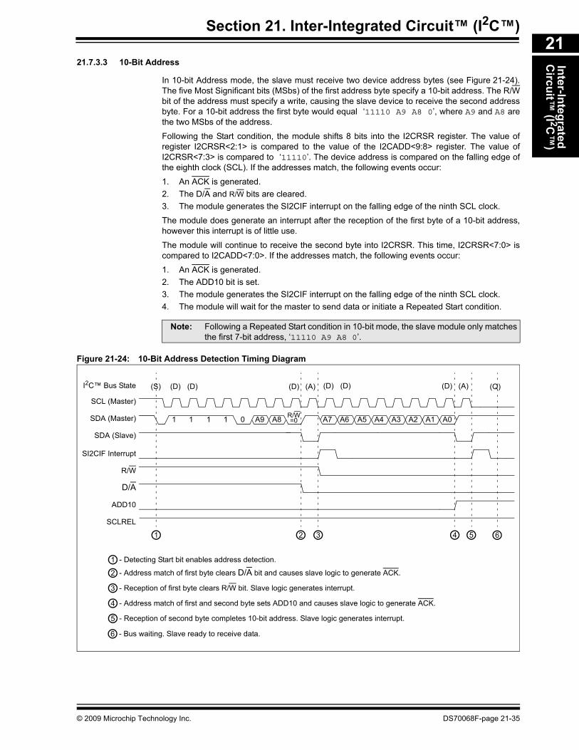
In 10-bit Address mode, the slave must receive two device address bytes (see Figure 21-24).The five Most Significant bits (MSbs) of the first address byte specify a 10-bit address. The R/Wbit of the address must specify a write, causing the slave device to receive the second addressbyte. For a 10-bit address the first byte would equal ‘11110 A9 A8 0’, where A9 and A8 arethe two MSbs of the address.
Following the Start condition, the module shifts 8 bits into the I2CRSR register. The value ofregister I2CRSR<2:1> is compared to the value of the I2CADD<9:8> register. The value ofI2CRSR<7:3> is compared to ‘11110’. The device address is compared on the falling edge ofthe eighth clock (SCL). If the addresses match, the following events occur:
1. An ACK is generated.2. The D/A and R/W bits are cleared.3. The module generates the SI2CIF interrupt on the falling edge of the ninth SCL clock.
The module does generate an interrupt after the reception of the first byte of a 10-bit address,however this interrupt is of little use.
The module will continue to receive the second byte into I2CRSR. This time, I2CRSR<7:0> iscompared to I2CADD<7:0>. If the addresses match, the following events occur:
1. An ACK is generated.2. The ADD10 bit is set.3. The module generates the SI2CIF interrupt on the falling edge of the ninth SCL clock.4. The module will wait for the master to send data or initiate a Repeated Start condition.
The addressing procedure for the I2C bus is such that the first byte after a Start condition usuallydetermines which slave device the master is addressing. The exception is the general calladdress, which can address all devices. When this address is used, all enabled devices shouldrespond with an Acknowledge. The general call address is one of eight addresses reserved forspecific purposes by the I2C protocol. It consists of all ‘0’s with R/W = 0. The general call isalways a slave write operation.
The general call address is recognized when the general call enable bit, GCEN (I2CCON<7>),is set (see Figure 21-25). Following a Start bit detect, 8 bits are shifted into the I2CRSR and theaddress is compared against the I2CADD, and is also compared to the general call address.
If the general call address matches, the following events occur:
1. An ACK is generated.2. Slave module will set the GCSTAT bit (I2CSTAT<9>). 3. The D/A and R/W bits are cleared.4. The module generates the SI2CIF interrupt on the falling edge of the ninth SCL clock.5. The I2CRSR is transferred to the I2CRCV and the RBF flag bit is set (during the eighth
bit).6. The module will wait for the master to send data.
When the interrupt is serviced, the cause for the interrupt can be checked by reading thecontents of the GCSTAT bit to determine if the device address was device specific or a generalcall address.
Note that general call addresses are 7-bit addresses. If A10M bit is set, configuring the slavemodule for 10-bit addresses and GCEN is set, the slave module continues to detect the 7-bitgeneral call address.
Some I2C system protocols require a slave to act upon all messages on the bus. For example,the Intelligent Platform Management Interface (IPMI) bus uses I2C nodes as message repeatersin a distributed network. To allow a node to repeat all messages, the slave module must acceptall messages, regardless of the device address.
Setting the IPMIEN bit (I2CCON<11>) enables this mode (see Figure 21-26). Regardless of thestate of the I2CADD register and the A10M and GCEN bits, all addresses will be accepted. Thisincludes all valid 7-bit addresses, General Call, Start Byte, CBUS, Reserved and HS modes, aswell as 10-bit address preambles.
If a 7-bit address does not match the contents of I2CADD<6:0>, the slave module will return toan Idle state and ignore all bus activity until after the Stop condition.
If the first byte of a 10-bit address does not match the contents of I2CADD<9:8>, the slavemodule will return to an Idle state and ignore all bus activity until after the Stop condition.
If the first byte of a 10-bit address matches the contents of I2CADD<9:8>, however, the secondbyte of the 10-bit address does not match I2CADD<7:0>, the slave module will return to an Idlestate and ignore all bus activity until after the Stop condition.
21.7.4 Receiving Data from a Master Device
When the R/W bit of the device address byte is zero and an address match occurs, the R/W bit(I2CSTAT<2>) is cleared. The slave module enters a state waiting for data sent by the master.After the device address byte, the contents of the data byte are defined by the system protocoland are only received by the slave module.
The slave module shifts 8 bits into the I2CRSR register. On the falling edge of the eighth clock(SCL), the following events occur:
1. The module begins to generate an ACK or NACK.2. The RBF bit is set to indicate received data.3. The I2CRSR byte is transferred to the I2CRCV register for access by the software.4. The D/A bit is set.5. A slave interrupt is generated. Software may check the status of the I2CSTAT register to
determine the cause of the event and then clear the SI2CIF flag.6. The module will wait for the next data byte.
Note: The user application must clear the IPMIEN bit during an I2C Master operation, andset it only while acting as an IPMI slave.
SCL (Master)
SDA (Master)
SDA (Slave)
SI2CIF Interrupt
2 31
- Detecting Start bit enables1
I2C™ Bus State (S) (D) (D) (A)(D) (Q)
R/W
D/A
I2CRCV
RBF
R/W
address detection.
- Regardless of contents of byte2address is matched.Address match clears D/A bit.
Normally, the slave module will Acknowledge all received bytes by sending an ACK on the ninthSCL clock. If the receive buffer is overrun, the slave module does not generate this ACK.Overrun is indicated if either (or both):
1. The buffer full bit, RBF (I2CSTAT<1>), was set before the transfer was received.2. The overflow bit, I2COV (I2CSTAT<6>), was set before the transfer was received.
Table 21-4 shows what happens when a data transfer byte is received, given the status of theRBF and I2COV bits. If the RBF bit is already set when the slave module attempts to transfer tothe I2CRCV, the transfer does not occur but the interrupt is generated and the I2COV bit is set.If both the RBF and I2COV bits are set, the slave module acts similarly. The shaded cells showthe condition where software did not properly clear the overflow condition. No reception or clockstretching occurs while I2COV bit is set.
Reading the I2CRCV clears the RBF bit. The I2COV bit is cleared by writing to a ‘0’ throughsoftware. This bit is also cleared automatically on a Stop or Repeat Start event.
Table 21-4: Data Transfer Received Byte Actions
21.7.4.2 WAIT States During Slave Receptions
When the slave module receives a data byte, the master can potentially begin sending the nextbyte immediately. This allows the software controlling the slave module 9 SCL clock periods toprocess the previously received byte. If this is not enough time, the slave software may want togenerate a bus WAIT period.
The STREN bit (I2CCON<6>) enables a bus WAIT to occur on slave receptions. WhenSTREN = 1 at the falling edge of the ninth SCL clock of a received byte, the slave module clearsthe SCLREL bit. Clearing the SCLREL bit causes the slave module to pull the SCL line low,initiating a WAIT. The SCL clock of the master and slave will synchronize, as shown in21.6.2 “Master Clock Synchronization”.
When the software is ready to resume reception, the software sets SCLREL. This causes theslave module to release the SCL line and the master resumes clocking.
Status Bits as DataByte Received Transfer
I2CRSR to I2CRCVGenerate
ACK
GenerateSI2CIF Interrupt(Interrupt occurs
if enabled)
SetRBF
SetI2COV
RBF I2COV
0 0 Yes Yes Yes Yes No change1 0 No No Yes No change Yes1 1 No No Yes No change Yes0 1 Yes No Yes Yes No change
Note: Shaded cells show state where the software did not properly clear the overflow condition.
Receiving a slave message is a rather automatic process. The software handling the slaveprotocol uses the slave interrupt to synchronize to the events.
When the slave detects the valid address, the associated interrupt will notify the software toperform a dummy read and expect a message. On receive data, as each data byte transfers tothe I2CRCV register, an interrupt notifies the software to unload the buffer.
Figure 21-27 shows a simple receive message. Being a 7-bit address message, only oneinterrupt occurs for the address bytes. Then, interrupts occur for each of four data bytes.
At an interrupt, the software may monitor the RBF, D/A and R/W bits to determine the conditionof the byte received.
Figure 21-28 shows a similar message using a 10-bit address. In this case, two bytes arerequired for the address.
Figure 21-29 shows a case where the software does not respond to the received byte and thebuffer overruns. On reception of the second byte, the module will automatically NACK the mastertransmission. Generally, this causes the master to resend the previous byte. The I2COV bitindicates that the buffer has overrun. The I2CRCV buffer retains the contents of the first byte. Onreception of the third byte, the buffer is still full and again the module will NACK the master. Afterthis, the software finally reads the buffer. Reading the buffer will clear the RBF bit, however theI2COV bit remains set. The software must clear the I2COV bit. The next received byte will bemoved to the I2CRCV buffer and the module will respond with a ACK.
Figure 21-30 highlights clock stretching while receiving data. Note in the previous examples,STREN = 0 which disables clock stretching on receive messages. In this example, the softwaresets STREN to enable clock stretching. When STREN = 1, the module will automatically clockstretch after each received data byte, allowing the software more time to move the data from thebuffer. Note that if RBF = 1 at the falling edge of the ninth clock, the module will automaticallyclear the SCLREL bit and pull the SCL bus line low. As shown with the second received data byte,if the software can read the buffer and clear the RBF before the falling edge of the ninth clock,the clock stretching will not occur. The software can also suspend the bus at any time. By clearingthe SCLREL bit, the module will pull the SCL line low after it detects the bus SCL low. The SCLline will remain low, suspending transactions on the bus until the SCLREL bit is set.
3 - Next byte received before I2CRCV read by software. I2CRCV register unchanged.I2COV overflow bit set. Slave generates interrupt. Slave sends NACK for reception.
N
4 - Next byte also received befo
Slave sends NACK for recepI2CRCV register unchanged
ure 21-30: Slave Message (Write Data to Slave: 7-Bit Address; Clock Stretching Enabled; A10M = 0; GCEN = 0; IP
1 - Software sets the STREN bit to enable clock stretching.
SCL (Master)
SDA (Master)
SCL (Slave)
SDA (Slave)
I2CTRN
TBF
I2CRCV
RBF
SI2CIF
STREN
1 2 3 4 5 6 7 8
A1A0
9
A
D7D6D5D4D3D2D1D0
1 2 3 4 5 6 7 8 9
W
32
A
5 3
2 - Slave receives address byte. I2CRCV register is read by user software to prevent
3 - Next received byte is message data. Byte moved to I2CRCV register, sets RBF.
6 - Software sets SCLREL bit to release c
7 - Slave does not clear SCLREL because
A6A5A4A3A2
S
P
I2COV
R/W
D/A
D7D6D5D4D3D2D1D0
1 2 3 4 5 6 7 8 9
A
D7
1
SCLREL
54 6 71
4 - Because RBF = 1 at ninth clock, automatic clock stretch begins. Slave clears SCLREL bit. Slave pulls SCL line low to stretch clock.
5 - Software reads I2CRCV register. RBF bit clears.
8 - Software may clear SCLREL to cause
9 - Software may set SCLREL to release a
before asserting SCL low.
buffer overflow.
dsPIC30F Family Reference Manual
21.7.5 Sending Data to a Master Device
When the R/W bit of the incoming device address byte is one and an address match occurs, theR/W bit (I2CSTAT<2>) is set. At this point, the master device is expecting the slave to respondby sending a byte of data. The contents of the byte are defined by the system protocol and areonly transmitted by the slave module.
When the interrupt from the address detection occurs, the software can write a byte to theI2CTRN register to start the data transmission. This will also set the D/A bit (I2CSTAT<5>).
The slave module sets the TBF bit. The eight data bits are shifted out on the falling edge of theSCL input. This ensures that the SDA signal is valid during the SCL high time. When all eightbits have been shifted out, the TBF bit will be cleared.
The slave module detects the Acknowledge from the master-receiver on the rising edge of theninth SCL clock.
If the SDA line is low indicating an Acknowledge (ACK), the master is expecting more data andthe message is not complete. The module generates a slave interrupt to indicate that more datais requested.
A slave interrupt is generated on the falling edge of the ninth SCL clock. Software must checkthe status of the I2CSTAT register and clear the SI2CIF flag.
If the SDA line is high, indicating a Not-Acknowledge (NACK), the data transfer is complete. Theslave module resets and generates an interrupt, and it waits for detection of the next Start bit.
21.7.5.1 WAIT States During Slave Transmissions
During a slave transmission message, the master expects return data immediately afterdetection of the valid address with R/W = 1. Because of this, the slave module will automaticallygenerate a bus WAIT whenever the slave returns data.
The automatic WAIT occurs at the falling edge of the ninth SCL clock of a valid device addressbyte or transmitted byte Acknowledged by the master, indicating expectation of more transmitdata.
The slave module clears the SCLREL bit. Clearing the SCLREL bit causes the slave module topull the SCL line low, initiating a WAIT. The SCL clock of the master and slave will synchronizeas shown in 21.6.2 “Master Clock Synchronization”.
When the software loads the I2CTRN and is ready to resume transmission, the software setsSCLREL. This causes the slave module to release the SCL line and the master resumesclocking.
21.7.5.2 Example Messages of Slave Transmission
Slave transmissions for 7-bit address messages are shown in Figure 21-31. When the addressmatches and the R/W bit of the address indicates a slave transmission, the module willautomatically initiate clock stretching by clearing the SCLREL bit and generate an interrupt toindicate a response byte is required. The software will write the response byte into the I2CTRNregister. As the transmission completes, the master will respond with an Acknowledge. If themaster replies with an ACK, the master expects more data and the module will again clear theSCLREL bit and generate another interrupt. If the master responds with a NACK, no more datais required and the module will not stretch the clock but will generate an interrupt.
Slave transmissions for 10-bit address messages require the slave to first recognize a 10-bitaddress. Because the master must send two bytes for the address, the R/W bit in the first byteof the address specifies a write. To change the message to a read, the master will send aRepeated Start and repeat the first byte of the address with the R/W bit specifying a read. At thispoint, the slave transmission begins as shown in Figure 21-32.
Note: When IPMIEN = 1 (IPMI mode), the I2C module assumes that the R/W bit is ‘0’.Therefore, the slave transmission function is disabled. If the R/W bit is ’1’, the I2Cmodule will trigger an interrupt. This interrupt should be ignored (i.e., the I2Cinterrupt flags should be cleared) and the I2C slave transmission event should beaborted.
By definition of the I2C bus being a wired AND bus connection, pull-up resistors on the bus arerequired, shown as RP in Figure 21-33. Series resistors, shown as RS are optional and used toimprove ESD susceptibility. The values of resistors RP and RS depend on the followingparameters:
• Supply voltage• Bus capacitance• Number of connected devices (input current + leakage current)
Because the device must be able to pull the bus low against RP, current drawn by RP must begreater than the I/O pin minimum sink current IOL of 3 mA at VOL(MAX) = 0.4V for the deviceoutput stage. For example, with a supply voltage of VDD = 5V + 10%:
In a 400 kHz system, a minimum rise time specification of 300 nsec exists and in a 100 kHzsystem, the specification is 1000 nsec.
Since RP must pull the bus up against the total capacitance CB with a maximum rise time of 300nsec to 0.7 VDD, the maximum resistance for RP must be less than:
The maximum value for RS is determined by the desired noise margin for the low level. RScannot drop enough voltage to make the device VOL plus voltage across RS more than themaximum VIL.
The SCL clock input must have a minimum high and low time for proper operation. The high andlow times of the I2C specification as well as the requirements of the I2C module, are shown inthe “Electrical Specifications” section in the specific device data sheet.
Figure 21-33: Sample Device Configuration for I2C™ Bus
RPRP
VDD + 10%
SDA
SCL
Device
CB = 10 - 400 pF
RSRS
Note: I2C™ devices with input levels related to VDD must have one common supply line to whichthe pull-up resistor is also connected.
The SCL and SDA pins have an input glitch filter. The I2C bus requires this filter in both the100 kHz and 400 kHz systems.
When operating on a 400 kHz bus, the I2C specification requires a slew rate control of thedevice pin output. This slew rate control is integrated into the device. If the DISSLW bit(I2CCON<9>) is cleared, the slew rate control is active. For other bus speeds, the I2Cspecification does not require slew rate control and DISSLW should be set.
Some system implementations of I2C busses require different input levels for VIL(MAX) andVIH(MIN).
In a normal I2C system:
• VIL(MAX) = lesser of 1.5V and 0.3 VDD
• VIH(MIN) = greater of 3.0V and 0.7 VDD
In a System Management Bus (SMBus) system:
• VIL(MAX) = 0.8V• VIH(MIN) = 2.1V
The SMEN bit (I2CCON<8>) controls the input levels. SMEN is set to change the input levels toSMBus specifications.
When the device executes a PWRSAV 0 instruction, the device enters Sleep mode. After thedevice returns to Operational mode, the master module will be in an Idle state waiting for amessage command and the slave module will be waiting for a Start condition.
There is no automatic method to prevent Sleep entry if a transmission or reception is active orpending. The software must synchronize Sleep entry with I2C operation to avoid incorrectmodule operation on device wake-up from sleep.
During Sleep, the slave module will not monitor the I2C bus. Thus, it is not possible to generatea wake-up event based on the I2C bus using the I2C module. Other interrupt inputs, such as theinterrupt-on-change inputs can be used to detect message traffic on a I2C bus and cause adevice wake-up.
21.9.2 When the Device Enters Idle Mode
When the device executes a PWRSAV 1 instruction, the device enters Idle mode. The modulewill enter a power-saving state in Idle mode depending on the I2CSIDL bit (I2CCON<13>).
If I2CSIDL = 1, the module will enter the Power-Saving mode similarly to actions while enteringSleep mode.
If I2CSIDL = 0, the module will not enter a Power-Saving mode. The module will continue tooperate normally.
21.10 Effects of a ResetA Reset disables the I2C module and terminates any active or pending message activity. Seethe register definitions of I2CCON and I2CSTAT for the Reset conditions of those registers.
Note: In this discussion, ‘Idle’ refers to the CPU power-saving state. The lower-case ‘idle’refers to the time when the I2C module is not transferring data on the bus.
Question 1: I am operating as a bus master and transmitting data, however, slave andreceive interrupts are also occurring.
Answer: The master and slave circuits are independent. The slave module will receive eventsfrom the bus sent by the master.
Question 2: I am operating as a slave and I write data to the I2CTRN register, but thedata did not transmit.
Answer: The slave enters an automatic wait when preparing to transmit. Ensure that you setthe SCLREL bit to release the I2C clock.
Question 3: How do I tell what state the master module is in?Answer: Looking at the condition of SEN, RSEN, PEN, RCEN, ACKEN and TRSTAT bits willindicate the state of the master module. If all bits are ‘0’, the module is Idle.
Question 4: Operating as a slave, I receive a byte while STREN = 0. What should thesoftware do if it cannot process the byte before the next one is received?
Answer: Because STREN was ‘0’, the module did not generate an automatic WAIT on thereceived byte. However, the software may, at any time during the message, set STREN thenclear SCLREL. This will cause a WAIT on the next opportunity to synchronize the SCL clock.
Question 5: My I2C system is a multi-master system. When I attempt to send a message,it is being corrupted.
Answer: In a multi-master system, other masters may cause bus collisions. In the InterruptService Routine for the master, check the BCL bit to ensure that the operation completedwithout a collision. If a collision is detected, the message must be resent from the beginning.
Question 6: My I2C system is a multi-master system. How can I tell when it is OK tobegin a message?
Answer: Look at the S and P bits. If S = 0 and P = 0 the bus is Idle. If S = 0 and P = 1, the busis Idle.
Question 7: I tried to send a Start condition on the bus, then transmit a byte by writingto the I2CTRN register. The byte did not get transmitted. Why?
Answer: You must wait for each event on the I2C bus to complete before starting the next one.In this case, you should poll the SEN bit to determine when the Start event completed, or wait forthe master I2C interrupt before data is written to I2CTRN.
21.13 Related Application NotesThis section lists application notes that are related to this section of the manual. Theseapplication notes may not be written specifically for the dsPIC30F Product Family, but theconcepts are pertinent and could be used with modification and possible limitations. The currentapplication notes related to the Inter-Integrated Circuit™ (I2C™) module are:
Title Application Note #Use of the SSP Module in the I 2C™ Multi-Master Environment AN578Using the PIC® Devices’ SSP and MSSP Modules for Slave I2C™ Communication AN734Using the PICmicro® MSSP Module for Master I2C™ Communications AN735An I2C™ Network Protocol for Environmental Monitoring AN736
Note: Please visit the Microchip web site (www.microchip.com) for additional ApplicationNotes and code examples for the dsPIC30F family of devices.
Revision A This is the initial released version of this document.
Revision BThis revision has been expanded to contain a full description of the dsPIC30F Inter-IntegratedCircuit (I2C) module.
Revision CThis revision incorporates all known errata at the time of this document update.
Revision DThis revision incorporates minor changes to the document text.
Revision EThis revision incorporates the following changes:
• Minor changes to the document text. • Updates were made to clarify the setting of the RBF bit and clock stretching (see
21.7.3 “Detecting the Address” and 21.7.4.3 “Example Messages of Slave Reception”). This change affects the following figures:- Figure 21-27: “Slave Message (Write Data to Slave: 7-Bit Address; Address


![[Andy Crowe PMP PgMP] the PMP Exam Quick Referen(BookZZ.org)](https://static.documents.pub/doc/80x56/577c79d11a28abe054940b45/andy-crowe-pmp-pgmp-the-pmp-exam-quick-referenbookzzorg.jpg)


