Page 1 of 17 Final Draft 18/03/15 01:00 p.m . MARKING SCHEME SET 55/1/B Q. No. Expected Answer / Value Points Marks Total Marks Section A Set1,Q1 Set2,Q5 Set3,Q2 It is a measure of the sharpness of resonance. Alternatively , / No unit ½ ½ 1 Set1,Q2 Set2,Q4 Set3,Q5 To convert one form of energy into another. (Alternatively , To convert other forms of energy into electrical energy) 1 1 Set1,Q3 Set2,Q2 Set3,Q4 1 1 Set1,Q4 Set2,Q3 Set3,Q1 Medium A 1 1 Set1,Q5 Set2,Q1 Set3,Q3 Line A represents parallel combination, Its slope is more(or It corresponds to a lower value of resistance) ½ + ½ 1 Section B Set1,Q6 Set2,Q7 Set3,Q10 It is the case of minimum deviation Alternatively, Deviation produced by prism here is minimum. ½ ½ ½ ½ ½ ½ Finding the angle of incidence 2 Downloaded From: http://www.cbseportal.com Downloaded From: http://www.cbseportal.com
Transcript
Page 1 of 17 Final Draft 18/03/15 01:00 p.m
.
MARKING SCHEME
SET 55/1/B
Q. No. Expected Answer / Value Points Marks Total
Marks
Section A
Set1,Q1
Set2,Q5
Set3,Q2
It is a measure of the sharpness of resonance.
Alternatively, /
No unit
½
½
1
Set1,Q2
Set2,Q4
Set3,Q5
To convert one form of energy into another.
(Alternatively, To convert other forms of energy into electrical energy)
1
1
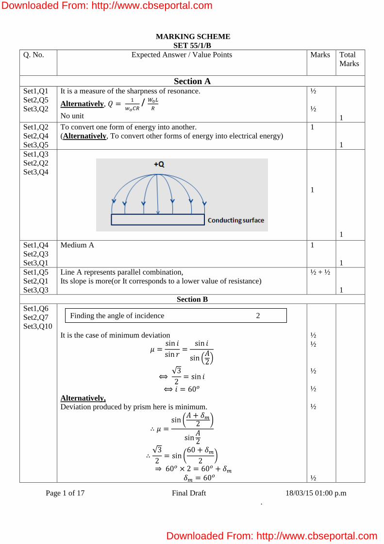
Set1,Q3
Set2,Q2
Set3,Q4
1
1
Set1,Q4
Set2,Q3
Set3,Q1
Medium A 1
1
Set1,Q5
Set2,Q1
Set3,Q3
Line A represents parallel combination,
Its slope is more(or It corresponds to a lower value of resistance)
½ + ½
1
Section B
Set1,Q6
Set2,Q7
Set3,Q10
It is the case of minimum deviation
Alternatively,
Deviation produced by prism here is minimum.
½
½
½
½
½
½
Finding the angle of incidence 2
Downloaded From: http://www.cbseportal.com
Downloaded From: http://www.cbseportal.com
Page 2 of 17 Final Draft 18/03/15 01:00 p.m
.
OR
Lens maker’s formula
= (n-1)
= (1.5-1)
=
=
Refractive index of the medium should be 1.5 (i.e. same as that of
material of lens)
½
½
½
½
½
½
2
2
Set1,Q7
Set2,Q10
Set3,Q8
In Ground state
K.E = = 13.6eV = 2.18 x 10⁻¹⁸
J
= = 0.33nm
[ Note: Award 1½ marks if student evaluates λ1 directly without calculating
E1]
Alternatively,
In first excited state, the de Broglie wavelength will increase.
½
1
½
2
Set1,Q8
Set2,Q6
Set3,Q9
Finding the focal length 1 ½
Value of refractive index ½
Determination of K.E ½
Wave length for ground state 1
Nature of change ½
i) Finding the K.E & P.E in Ground state ½ +½
ii) Finding the K.E & P.E in Second excited state ½ +½
Downloaded From: http://www.cbseportal.com
Downloaded From: http://www.cbseportal.com
Page 3 of 17 Final Draft 18/03/15 01:00 p.m
.
For Ground state,
K.E =13.6 eV ( K.E = - T.E)
P.E = - 27.2 eV ( P.E = 2 T.E)
For second Excited state (n=3)
K.E = - ) eV = 1.51 eV
P.E = -3.02 eV
[ Award ½ mark if the student does the calculations by taking n=2 ]
½
½
½
½
2
Set1,Q9
Set2,Q8
Set3,Q7
Space Wave Sky Wave
In space wave mode, the waves
travel in straight line directly from
transmitter to receiver
Reflected by Ionosphere
Because frequencies is greater than 40 MHz penetrate the ionosphere.
(Alternatively: There frequencies (greater than 40 MHz) are not reflected by
the ionosphere)
1
1
2
Set1,Q10
Set2,Q9
Set3,Q6
a) Balance Point will be shifted towards B.
The potential gradient will decrease and hence the balancing length will
increase.
b) No effect on balance point.
At balance point no current flows through resistor S.
½
½
½
½
2
Section C
Set1,Q11
Set2,Q20
Set3,Q15
The capacitance of both the capacitors increases by a factor K.
a) New Electric field energy values are:
b) New charges are:
½ + ½
½ + ½
Distinguishing between sky wave and space wave mode 1
Reason 1
Shift in balance point for part ‘a’ and ‘b’ 1
Reason 1
Effect of dielectric on
a) Electric field energy ½ +½
b) Charge ½ +½
c) Potential difference ½ +½
Downloaded From: http://www.cbseportal.com
Downloaded From: http://www.cbseportal.com
Page 4 of 17 Final Draft 18/03/15 01:00 p.m
.
c) New P.Dvalues are:
(The battery remains connected to the capacitors)
Alternatively: The student may assumes that the battery has been removed.
a) New Electric field energy values are:
b) New charges are:
Q and Q as before
c) New P.D values are:
½ + ½
½ + ½
½ + ½
½ + ½
3
Set1,Q12
Set2,Q21
Set3,Q16
The rate at which the nuclei of the radioactive sample disintegrate.
[Alternatively, ]
SI Unit – becquerel / disintegration per second/
Half Life = 10 hrs.
(Given : Activity becomes half after 10 hrs )
Activity after 20 hrs
(= 2× half life )
= of intial activity
Intial activity
= 10000× 4 dps
= 40000dps
Alternatively :
By dividing
½
½
½
½
½
½
Definition of activity and SI unit 1
Calculation of half life +Activity 1½+½
Downloaded From: http://www.cbseportal.com
Downloaded From: http://www.cbseportal.com
Page 5 of 17 Final Draft 18/03/15 01:00 p.m
.
Initial activity = 10000 × = 40000 dps
½
3
Set1,Q13
Set2,Q22
Set3,Q17
(a) The intensity of inteferance fringes in double slit arrangement is
modulated by the diffraction pattern of each slit.
Alternatively, In double slit experiment the interference pattern on the screen
is actually superposition of single slit diffraction for each slit.
(b) Waves diffracted from the edges of the circular obstacle interfere
constructively at the centre of the shadow producing a bright spot.
(c) Resolving power =
Resolving power is inversely propotional to wavelength and directly
proportional to the refractive index.
Alternatively :
(i) R.P
(ii) R.P
1
1
½
½
3
Set1,Q14
Set2,Q16
Set3,Q18
Definition : It is defined as the number of photons (of given
frequency)incident per unit area per unit time.
[Alternatively,
=
= - )eV
= 4.2 eV (also accept the answer in joules)
For red light incident photon energy will be less than the work function,
hence no emission of electrons.(Also accept : There would be no
photoemission)
1
½
½
½
½
3
Answers of part (a), (b), (c) 1+1+1
Definition of Intensity of radiation 1
Calculation of work function 1 ½
Response to red light ½
Downloaded From: http://www.cbseportal.com
Downloaded From: http://www.cbseportal.com
Page 6 of 17 Final Draft 18/03/15 01:00 p.m
.
OR
Incident photon energy( is used up in two ways:
(1) A part of this energy is used to remove the electrons.
(2) Remaining part of the energy imparts KE to the emitted electrons
Explanation :
(i)Maximum KE depends on frequency and not on intensity.
(ii) There exists a threashold frequency (for which ) below
which no photoemission takes place.
(iii)Basic elementary process involved is absorption of photon by e-. This
process is instantaneous.
(Any Two)
½
½
1+1
3
Set1,Q15
Set2,Q17
Set3,Q11
a) Microwaves
b) Electric charges can acquire energy and momentum from e.m. waves.
c)
1
1
½ + ½
3
Set1,Q16
Set2,Q18
Set3,Q12
Explanation : For diamagnetic material resultant magnetic moment in an
atom is zero. In presence of external magnetic field, they acquire a net
magnetic moment in a direction opposite to applied field. (or get repellled)
In paramagnetic material there is a permanent magnetic dipole moment of
atoms. The external magnetic field tends to align these along its own
direction. (or attracts them).
1 + 1
½
½
3
Set1,Q17
Set2,Q19
Set3,Q13
Photo electric equation 1
Explanation of observations (any two) 1+1
Answers of parts (a), (b) & (c) 1+1+1
Drawing of magnetic field lines 1+1
Explanation ½ + ½
Explanation of two processes with diagram 1+1
Definition of depletion region & barrier potential ½ + ½
Downloaded From: http://www.cbseportal.com
Downloaded From: http://www.cbseportal.com
Page 7 of 17 Final Draft 18/03/15 01:00 p.m
.
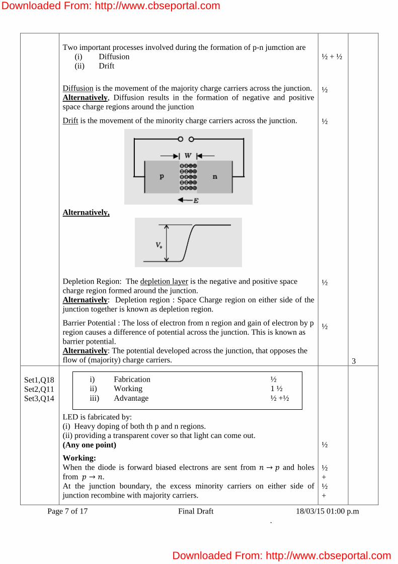
Two important processes involved during the formation of p-n jumction are
(i) Diffusion
(ii) Drift
Diffusion is the movement of the majority charge carriers across the junction.
Alternatively, Diffusion results in the formation of negative and positive
space charge regions around the junction
Drift is the movement of the minority charge carriers across the junction.
Alternatively,
Depletion Region: The depletion layer is the negative and positive space
charge region formed around the junction.
Alternatively: Depletion region : Space Charge region on either side of the
junction together is known as depletion region.
Barrier Potential : The loss of electron from n region and gain of electron by p
region causes a difference of potential across the junction. This is known as
barrier potential.
Alternatively: The potential developed across the junction, that opposes the
flow of (majority) charge carriers.
½ + ½
½
½
½
½
3
Set1,Q18
Set2,Q11
Set3,Q14
LED is fabricated by:
(i) Heavy doping of both th p and n regions.
(ii) providing a transparent cover so that light can come out.
(Any one point)
Working:
When the diode is forward biased electrons are sent from and holes
from .
At the junction boundary, the excess minority carriers on either side of
junction recombine with majority carriers.
½
½
+
½
+
i) Fabrication ½
ii) Working 1 ½
iii) Advantage ½ +½
Downloaded From: http://www.cbseportal.com
Downloaded From: http://www.cbseportal.com
Page 8 of 17 Final Draft 18/03/15 01:00 p.m
.
This releases energy in the form of photon .
Advantages (any two)
Low operational voltage
Long life
Fast on /off switching capability
No warm up time required
½
½ + ½
3
Set1,Q19
Set2,Q12
Set3,Q21
[Full credit for this part maybe given to the student. ]
=
= 0.75× 12 = 9 V
2
½
½
3
Set1,Q20
Set2,Q13
Set3,Q22
The basic phenomenon / process which occurs is polarisation.
The incident unpolarised sun ligh encounte the molecules of earth’s
atmosphere. Under the influence of electric field of incident wave the in
the molecule acquires component of motion in both these direction. If an
observer is looking 900 to the direction of the Sun ,charge accelarating
parallel to double arrow do not radiate energy towards the observer.[Their
accelaration has no transverse component.] This explain polarisation of
scattered light from sky.
b)
½
½
½
½
Block diagram 2
Calculation of 1
a) Explanation of the phenomenon using diagram 1½
b) Explanation of polarisation of Reflected light.
Derivation of Brewster’s Law 1½
Downloaded From: http://www.cbseportal.com
Downloaded From: http://www.cbseportal.com
Page 9 of 17 Final Draft 18/03/15 01:00 p.m
.
When unpolarised light is incident at polarising angle, at the interface of a
refracting medium, the reflected ray being perpendicular to the refracted ray
is completely polarised.
Now
This is Brewter’s Law
½
½
3
Set1,Q21
Set2,Q14
Set3,Q19
For an ideal inductor connected to ac source
=
=
=
(Also accept any other correct method)
Power factor cos∅ = R/Z
For LR circuit, at XL = R
Z =
Z = R
= cos = =
For LCR circuit
Z = = R
½
½
½
½
½
i) Derivation of the Average power in inductor 1½
ii) Ratio of Power factors and 1½
Downloaded From: http://www.cbseportal.com
Downloaded From: http://www.cbseportal.com
Page 10 of 17 Final Draft 18/03/15 01:00 p.m
.
Power factor P2 = = 1
=> =
[Award 1½mark if the student writes directly :
]
½
3
Set1,Q22
Set2,Q15
Set3,Q20
Resistivity of a conductor is defined as the resistance of a material (of a
Conductor) of unit length and unit area of cross section.
(Alternatively, ρ = )
Conductor Semiconductor
In conductor with increase in temperatures relaxtion time decreases, but
number density of charge carriers is not dependent on temperature. Hence,
increases.
In semiconductors number density of charge carriers increases with
temperature, it dominates the decrease in relaxtion time. Hence,
decreases.
1
½ + ½
½
½
3
Section D
Set1,Q23
Set2,Q23
Set3,Q23
a) Asha and her family helpful, concern for others , caring nature (any two)
Doctor was generous, helping nature, caring (any two)
(Any other alternative correct value should be accepted )
b) High magnetic field required. / (Expensive set up needed) Any other
correct answer
[Note: Full credit of ½ mark may be given [for this part to all students]
1
1
½
Definition of resistivity 1
Graphs ½ +½
Explanation ½ +½
Values displayed 2
Answer of part (b) ½
Maximum & Minimum force 1 +½
Downloaded From: http://www.cbseportal.com
Downloaded From: http://www.cbseportal.com
Page 11 of 17 Final Draft 18/03/15 01:00 p.m
.
= 1.6 ×
½
½
½
4
Section E
Set1,Q24
Set2,Q26
Set3,Q25
a)
Torque experienced by an electric dipole
Work done by external torque
When θ1 = 900, and θ2 = θ
For stable equillibrium
Unstable equillibrium
½
½
½
½
½
½
a) Derivation of potential energy of dipole 2
Angle for stable and unstable equilibrium ½ + ½
b) Dependence of potential on r 2
Downloaded From: http://www.cbseportal.com
Downloaded From: http://www.cbseportal.com
Page 12 of 17 Final Draft 18/03/15 01:00 p.m
.
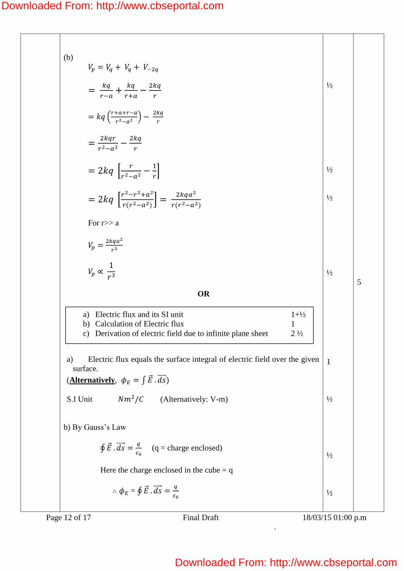
(b)
For r>> a
OR
a) Electric flux equals the surface integral of electric field over the given
surface.
(Alternatively,
S.I Unit (Alternatively: V-m)
b) By Gauss’s Law
(q = charge enclosed)
Here the charge enclosed in the cube = q
=
½
½
½
½
1
½
½
½
5
a) Electric flux and its SI unit 1+½
b) Calculation of Electric flux 1
c) Derivation of electric field due to infinite plane sheet 2 ½
Downloaded From: http://www.cbseportal.com
Downloaded From: http://www.cbseportal.com
Page 13 of 17 Final Draft 18/03/15 01:00 p.m
.
c)
+ +
= EA + EA + 0 = 2EA
By Gauss Law,
∴ =
∴ E is independent of x
½
½
1
½
½
5
Set1,Q25
Set2,Q24
Set3,Q26
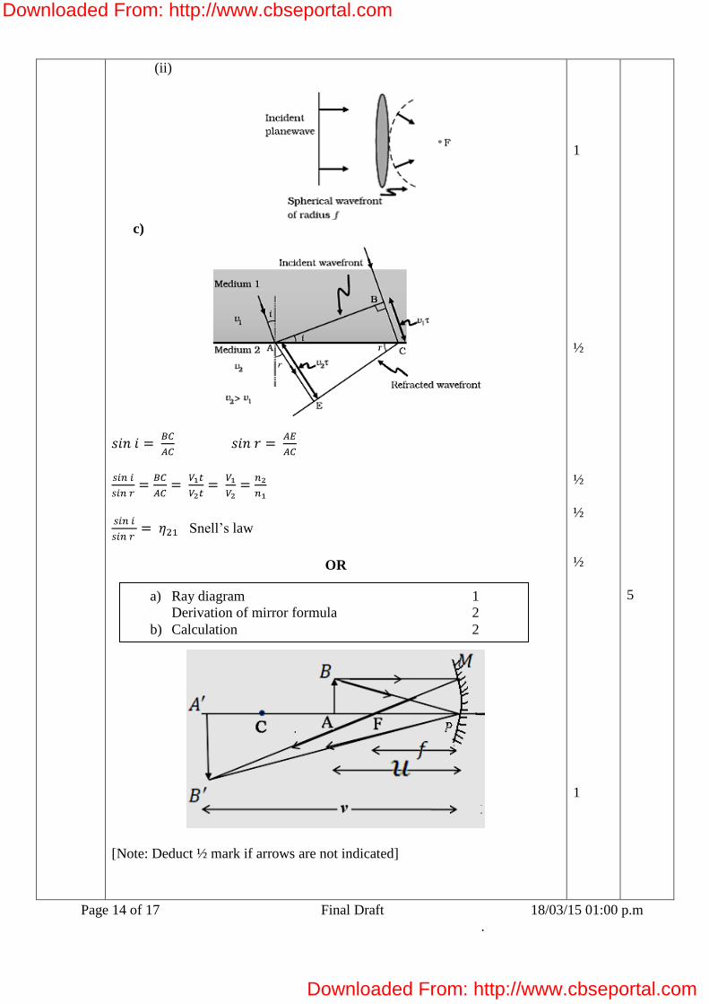
a) Locus of all the points which are in same phase / surface of constant
phase
b) (i)
1
1
a) Definition of wave front 1
b) Diagram of wave fronts for
(i) Reflection of plane wave by concave mirror 1
(ii) Refraction of plane wave by convex lens 1
c) Verification of Snell’s Law/ 2
Downloaded From: http://www.cbseportal.com
Downloaded From: http://www.cbseportal.com
Page 14 of 17 Final Draft 18/03/15 01:00 p.m
.
(ii)
c)
Snell’s law
OR
[Note: Deduct ½ mark if arrows are not indicated]
1
½
½
½
½
1
5
a) Ray diagram 1
Derivation of mirror formula 2
b) Calculation 2
Downloaded From: http://www.cbseportal.com
Downloaded From: http://www.cbseportal.com
Page 15 of 17 Final Draft 18/03/15 01:00 p.m
.
In
In
But
∴ =
Dividing by
b) Here the object is virtual and image is real cm
(i)
=
from the lens
(ii)
from the lens
½
½
½
½
½
½
½
½
5
Set1,Q26
Set2,Q25
Set3,Q24
a) Description with diagram 1 +1
Statement of Faraday’s law 1
b) Answers and their justification
parts (i) & (ii) 1+1
Downloaded From: http://www.cbseportal.com
Downloaded From: http://www.cbseportal.com
Page 16 of 17 Final Draft 18/03/15 01:00 p.m
.
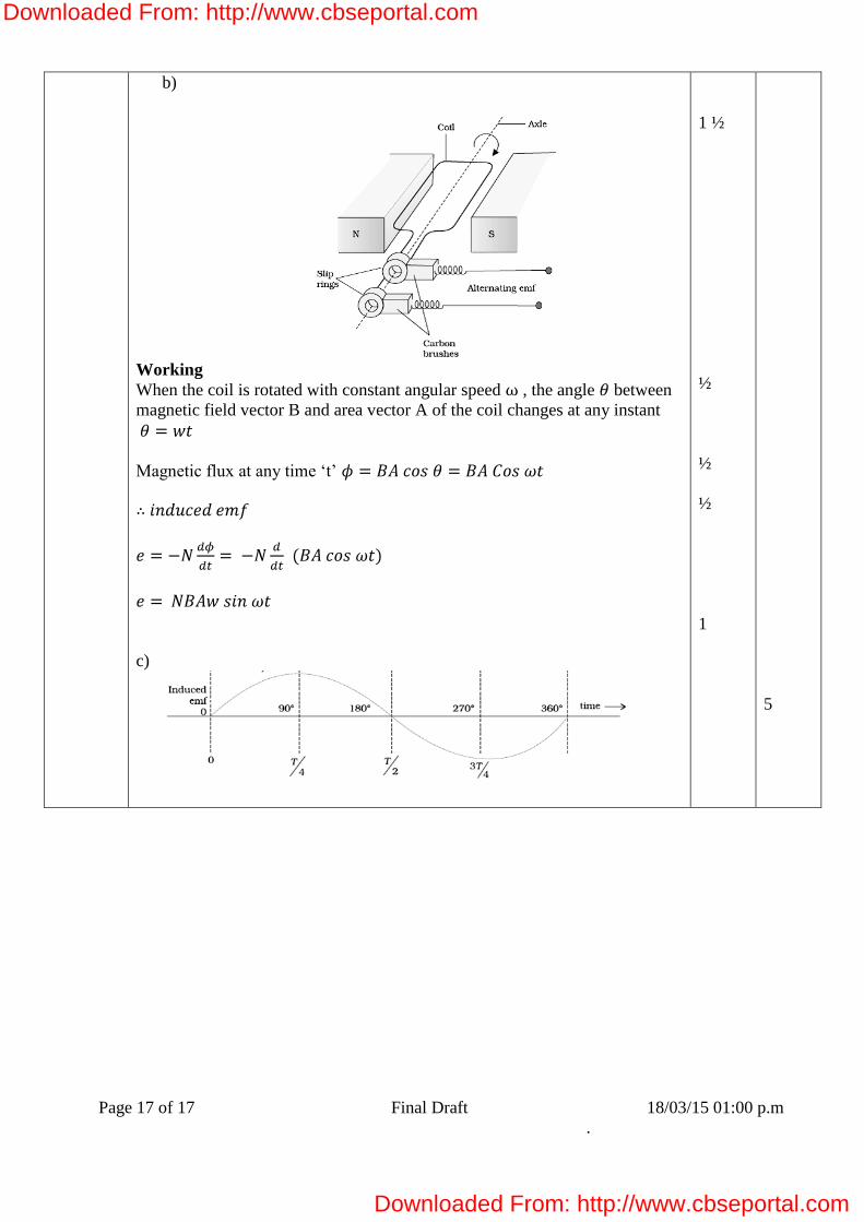
a)
(Also accept any other correct figure)
When the bar magnet moves towards the coil, connected to a Galvanometer.
The Galvanometer shows a deflection. This is due to change in the magnetic
field/flux, linked with the coil. This shows that an emf is induced.
The magnitude of emf induce is directly proportional to the rate of change of
magnetic flux in the circuit .
b) (i) the emf induced
Emf will be more in case of square loop as the side perpendicular to the
velocity is longer as compared to the rectangular loop.
(ii) Current will be less in rectangular loop, as it has more resistance and less
induced emf.
[Note: also accept if the student says
(i) emf induced will be zero in both cases as long as the coils stay in
the field.
(ii) current will be zero in both the cases as long as the coils stays in
the field.
OR
a) Principle : Electromagnetic induction; effective area of the loop
( = A cos θ), exposed to the magnetic field, keeps on changing as the
coil rotates.
[Alternatively: Whenever magnetic flux linked with a coil changes, an
emf is setup in the coil]
1
1
1
½
½
½ + ½
½ + ½
½ + ½
1
5
a. Principle of a.c. generator 1
b. Explanation of working with labeled diagram
and obtaining the expression of emf 3
c. Schematic diagram 1
Downloaded From: http://www.cbseportal.com
Downloaded From: http://www.cbseportal.com
Page 17 of 17 Final Draft 18/03/15 01:00 p.m
.
b)
Working
When the coil is rotated with constant angular speed ω , the angle between
magnetic field vector B and area vector A of the coil changes at any instant