CEG 360/560; EE 451/651 Digital System Design Dr. Travis Doom, Associate Professor Department of Computer Science and Engineering Wright State University Section I: Section I: Digital System Analysis and Review Digital System Analysis and Review CEG 360/560 - EE 451/651 Section I -2 Acknowledgements Acknowledgements These slides were developed with the aid of examples found in: – “Digital Design” – Frank Vahid – “Logic and Computer Design Fundamentals” - M. Morris Mano – “Digital Design: Principles and Practices” - John Wakerly The original version of many of the “Wakerly” slides were kindly provided by: – Dr. Roger L. Haggard et al CEG 360/560 - EE 451/651 Section I -3 Outline Outline Review of Combinational Logic Concepts What is Sequential Logic? – Bi-stable Logic Elements and Metastability Basic Sequential Devices – Flip-flops: Type, Function, and Structure – Characteristic Equations The Clocked Synchronous State Machine (CSSM) – Analysis of State Machines General structure, Analysis procedure CSSM Models: Mealy Vs. Moore – Methods of Representation State tables and diagrams – Timing Calculating Setup Time, Hold Times, and Maximum clock rate
Transcript
CEG 360/560; EE 451/651 Digital System Design
Dr. Travis Doom, Associate ProfessorDepartment of Computer Science and Engineering
Wright State University
Section I: Section I: Digital System Analysis and ReviewDigital System Analysis and Review
CEG 360/560 - EE 451/651 Section I - 2
AcknowledgementsAcknowledgements
These slides were developed with the aid of examples found in:– “Digital Design” – Frank Vahid– “Logic and Computer Design Fundamentals” - M. Morris Mano– “Digital Design: Principles and Practices” - John Wakerly
The original version of many of the “Wakerly” slides were kindly provided by:
– Dr. Roger L. Haggard et al
CEG 360/560 - EE 451/651 Section I - 3
OutlineOutline
Review of Combinational Logic ConceptsWhat is Sequential Logic?
– Bi-stable Logic Elements and MetastabilityBasic Sequential Devices
– Flip-flops: Type, Function, and Structure– Characteristic Equations
The Clocked Synchronous State Machine (CSSM)– Analysis of State Machines
General structure, Analysis procedureCSSM Models: Mealy Vs. Moore
– Methods of RepresentationState tables and diagrams
– TimingCalculating Setup Time, Hold Times, and Maximum clock rate
CEG 360/560 - EE 451/651 Section I - 4
Logic DevicesLogic Devices
Logic devices divide into two major types:
Combinational Logic– Current output depends on current input only– Examples: gates, decoders, multiplexors (MUXs), ALUs– Familiarity with combinational logic is a course prerequisite
Sequential Logic– Current output depends on past inputs as well as current input– Thus has a memory (usually called the state)– Examples: latches, flip-flops, state machines, counters, shift registers
CEG 360/560 - EE 451/651 Section I - 5
Basic Logic GatesBasic Logic Gates
AND gate– Output Z = 1 only when inputs A and B are both 1
OR gate– Output Z = 1 only when inputs A or B or both are 1
NOT gate or inverter– Output Z = 1 only when input A is 0
Simple alone, but combine a few million gates properly and you have a computer!
A
BZ
A
BZ
ZA
CEG 360/560 - EE 451/651 Section I - 6
Gate SymbolsGate Symbols
OR
NOR
AND
NAND
INVERTER
BUFFER
Exercise: show that the equivalent gates do the same function
CEG 360/560 - EE 451/651 Section I - 7
Logic DiagramLogic Diagram
Good Design Practices include:– Bubble-to-Bubble logic– All wires are either horizontal or vertical– All wires are labeled with expression– Wires are connected at “T” intersections– Wires are not connected at “X” intersections
Schematic diagrams should include– IC-Type-Logic Family– Pin numbers- Pin Diagram– Reference designator- Unit Number
Purpose : To make it easy to understand the function of the Logic circuit
ERROR/ FAIL
/ OVERFLOWERROR
/ FAIL
/ OVERFLOW≡
CEG 360/560 - EE 451/651 Section I - 9
Digital DevicesDigital Devices
Analog characteristics– Continuous signal levels– Very small, smooth level changes
Digital characteristics– Discrete signal levels (voltage usually)– Two levels: on/off, high/low 1/0 (binary)– Disjoint or quantized level changes
Digital Concepts and Devices– Digital Design also called Logic Design– Logic Gates - the most basic digital devices – Digital devices have analog electronic aspects
Exercise: list some of these aspects
t
v
v
t
CEG 360/560 - EE 451/651 Section I - 10
Electronic Aspects of Digital DesignElectronic Aspects of Digital Design
Vin low → Ib = 0– transistor cut off: Vout = Vcc
Vin high → Ib > 0– transistor “on”: Vout = GND
Vin
Vout
GND
Vcc
Rc
Rb
VccVIHminVOLmax
Vin
VOLmax
VOHmin
GND
Vcc
VCESat
Vout
Abnormal except for switching
VOLmax: max output voltage in low state
VOHmin: min output voltage in high state
VILmax: max input voltage recognized as low
VIHmin: min input voltage recognized as high
CEG 360/560 - EE 451/651 Section I - 11
Electronic Aspects of Digital DesignElectronic Aspects of Digital Design
Digital devices are built with analog componentsA range of voltages associated with each logic value ( 0 or 1 )Noise margin : The difference between the range boundaries
– in low state = VILmax - VOLmax = 1.5 V - 0.1 V= 1.4 V for 5V CMOS– in high state = VOHmin - VIHLmin = 4.9 V - 3.5 V= 1.4 V for 5V CMOS
Voltage OutputsNoiseMargin Inputs
Logic 0 Logic 0
Logic 1 Logic 1
Invalid
CEG 360/560 - EE 451/651 Section I - 12
Electronic Aspects of Digital DesignElectronic Aspects of Digital Design
Logic gates Specifications : - Conditions under which the digital device produces and recognizes
logic signals within the appropriate range.
- Examples :- Power-supply voltage- Temperature - Loading - Frequency
Manufacturer specifications ( data sheets )
CEG 360/560 - EE 451/651 Section I - 13
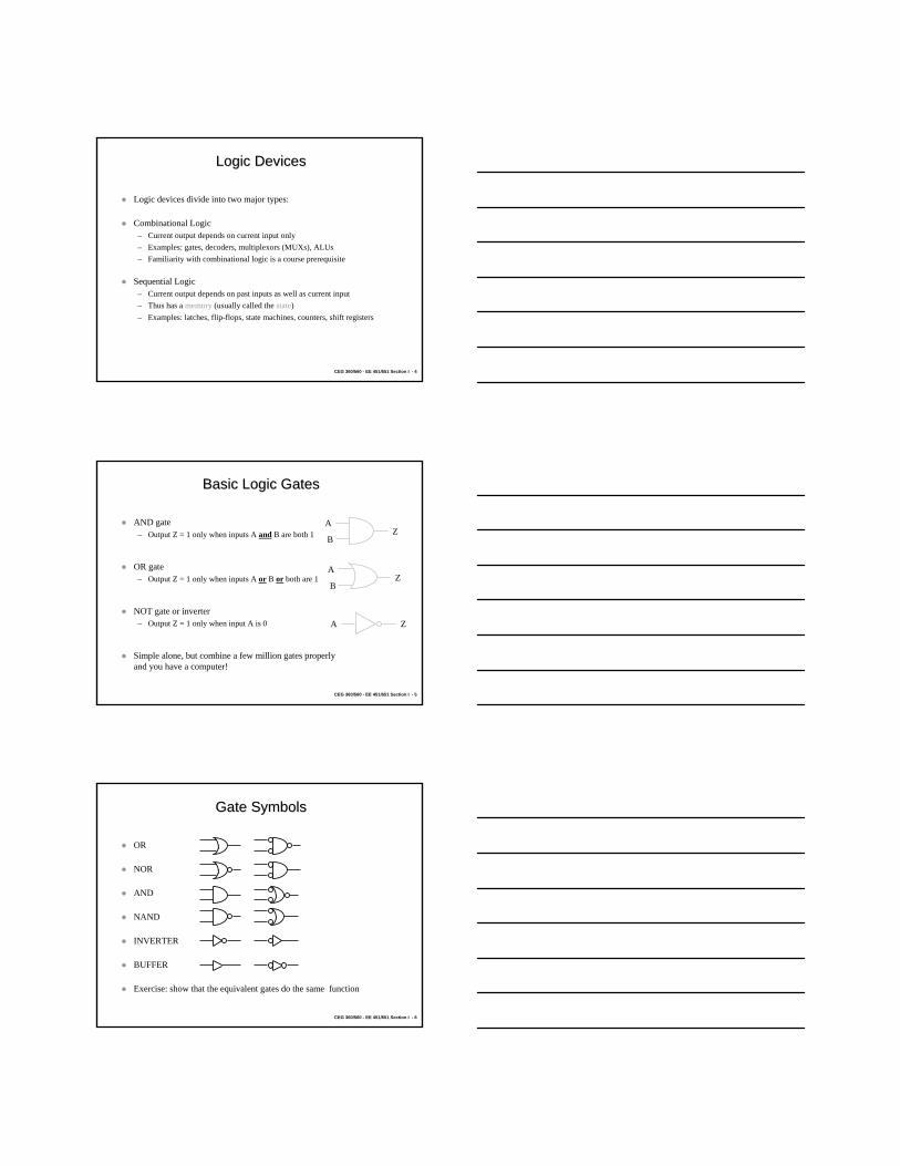
Propagation DelayPropagation Delay
The delay time between input transitions and the output transitions due to the propagation delay of the the logic gates.tp of a signal depends on the signal path inside the logic circuitFor a logic gate tpLH may not equal tpHL
tp is specified in the manufacturer data sheets of the IC’sExample : -The time delay for 74x00 in nanoseconds for three logic Families:
Typical MaximumtpLH tpHL tpLH tpHL
74LS00 9 10 15 1574HCT00 11 11 35 35 74ACT00 5.5 4.0 9.5 8.0To find tp for a signal, add the propagation delays of all gates along thepath of the signal
CEG 360/560 - EE 451/651 Section I - 14
Timing DiagramsTiming DiagramsY
X
X
Y
tpLH(XY) tpHL(XY) trise tfall
Actual Timing Diagram
Functional Timing Diagram
X
Y
Functional timing diagrams do not show exact delays.“lining up” everything allows the diagram to display more clearly which functions are performed in response to which action
– Illustrates operation, but does not specify upper and lower limits– Not always sufficient for a real design
CEG 360/560 - EE 451/651 Section I - 15
DecoderDecoderMultiple-input/multiple-output device.Decoder - Inputs (n) < outputs (m).Encoder - Inputs (n) > outputs (m)Converts input code words into output code words.One-to-One mapping :- Each input code produces only one
Iterative logic array: A device consisting of identical sub-circuits connected together in a chain to perform a larger overall functionIterative Comparator : cascaded 1-bit comparators1-bit comparator :
Function Table EQI X Y EQO
0 x x 0 1 0 0 1 1 0 1 0 1 1 0 0 1 1 1 1
X Y
EQI
EQO
X Y
EQI EQO
X0 Y0
EQ0 =1 EQ1X Y
EQI EQO
X1 Y1
EQ1X Y
EQI EQO
X(N-1) Y(N-1)
EQNEQ1(N-1)
CEG 360/560 - EE 451/651 Section I - 19
MSI Arithmetic Logic Units (ALU )MSI Arithmetic Logic Units (ALU )
ALU performs Arithmetic and Logical Functions - A , B : 4 bits inputs- S3,S2,S1,S0 : Function select- M=0 : Arithmetic operations +=Plus , - = Minus
MultiplexersMultiplexersMultiplexing: transmitting large number of signals over a small number of channels or linesDigital multiplexer (MUX): selects one of many input lines and directs it to a single output (often a bus or “party line”).Selection lines controls the selection of a particular inputm-bit 2n x 1 multiplexer:
– n selection lines, 2n m-bit inputs, 1 m-bit output.Example : 4-to-1 line multiplexer:Function Table :
Any n-variable logic function can be implemented using a 2n-to-1 MUX– (In fact, MUXs are a universal device! Any combinational function can be
implemented using only MUXes).The inputs variables are connected to the select input.The function value for each input combination (0 or 1) is connected to the corresponding input of the MUX
Example:
Row X Y F0 0 0 01 0 1 12 1 0 03 1 1 1
4 1×MUX
I0
Y
S1 S0
FI1
I2
I3
XY
0
1
0
1
CEG 360/560 - EE 451/651 Section I - 22
Functional Decomposition Functional Decomposition
Effective way for using MUX to implement Logic Functions.n-variable truth table can be simplified using any MUX :– Use one or more variables as control inputs– Decompose the remaining logic function in terms of the remaining inputs
– For 3-variable Logic Function , the decomposed truth table is :
Row X Y Z F0,1 0 0 x F00(Z)2,3 0 1 x F01(Z) 4,5 1 0 x F10(Z) 6,7 1 1 x F11(Z)
Values of Fxx(Z) = 0 or 1 or Z or Z’
4 1×MUX
I0
Y
S1 S0
FI1
I2
I3
XY
F00(Z)F01(Z)F10(Z)F11(Z)
CEG 360/560 - EE 451/651 Section I - 23
DemultiplexersDemultiplexers
Demultiplexer (DMUX) performs the opposite function of a MUX.A digital Demultiplexer receives input data on a single input and transmits it on one of 2^n possible outputs according to the value of the n select inputs MUX/DMUX are used in data transmission
Review of Combinational Logic ConceptsWhat is Sequential Logic?
– Bi-stable Logic Elements and MetastabilityBasic Sequential Devices
– Flip-flops: Type, Function, and Structure– Characteristic Equations
The Clocked Synchronous State Machine (CSSM)– Analysis of State Machines
General structure, Analysis procedureCSSM Models: Mealy Vs. Moore
– Methods of RepresentationState tables and diagrams
– TimingCalculating Setup Time, Hold Times, and Maximum clock rate
CEG 360/560 - EE 451/651 Section I - 26
STATE- A collection of state variables whose values at any one time contain all the information about the past values necessary to account for future behavior.
Example: A TV tuner could have a current channel stored internally, so the next channel can be predicted as a function of the inputs, i.e. the UP button increases the channel by one, the DOWN button decreases the channel by one. What is the state of this TV tuner?
Digital sequential logic– State variables are binary values– Circuit with n binary state variables has 2n possible states– Also known as a finite state machine (FSM).– Changes usually synchronized with a system clock
Sequential Logic Definitions
CEG 360/560 - EE 451/651 Section I - 27
Bistable ElementBistable Element
The simplest possible feedback sequential logic circuit is shown below:
It is bistable because it has two stable states:– State 1: If Q (Q=Vout1=Vin2) is high, the bottom inverter output
(/Q =Vout2=Vin1) is low, which keeps the top inverter output Q high.– State 2: If Q is low, the bottom inverter output /Q is high, which keeps the
top inverter output Q low.
Vin1
Vin2
Vout1
Vout2
Q
/Q
CEG 360/560 - EE 451/651 Section I - 28
Analog Analysis of a BistableAnalog Analysis of a Bistable
Q Vout1 Vin2
Vin1 Vout2 /Q
Vout1=Vin2
Top Inverter alone Bottom Inverter alone
Complete Bistable
Vin1=Vout2
Stable High
Stable Low
Metastable
CEG 360/560 - EE 451/651 Section I - 29
Bistable Devices and Bistable Devices and MetastabilityMetastability
There are not two stable states, but three (a problem!)A metastable point occurs when both outputs are halfway between high and low, the resulting output is not a valid logic level.Metastability could last forever, but noise usually pushes towards a stable state (HIGH or LOW).Noise in a bistable state returns it to the same stable stateEvery input pulse must remain stable “long enough”
– This is the minimum pulse width for the bistable elementAnalogous to a ball on a hill:
Store a data bit, not set/resetThe “Transparent” latchNo illegal operation problem
DC
S
R
Q
QC
CEG 360/560 - EE 451/651 Section I - 33
OutlineOutline
Review of Combinational Logic ConceptsWhat is Sequential Logic?
– Bi-stable Logic Elements and MetastabilityBasic Sequential Devices
– Flip-flops: Type, Function, and Structure– Characteristic Equations
The Clocked Synchronous State Machine (CSSM)– Analysis of State Machines
General structure, Analysis procedureCSSM Models: Mealy Vs. Moore
– Methods of RepresentationState tables and diagrams
– TimingCalculating Setup Time, Hold Times, and Maximum clock rate
CEG 360/560 - EE 451/651 Section I - 34
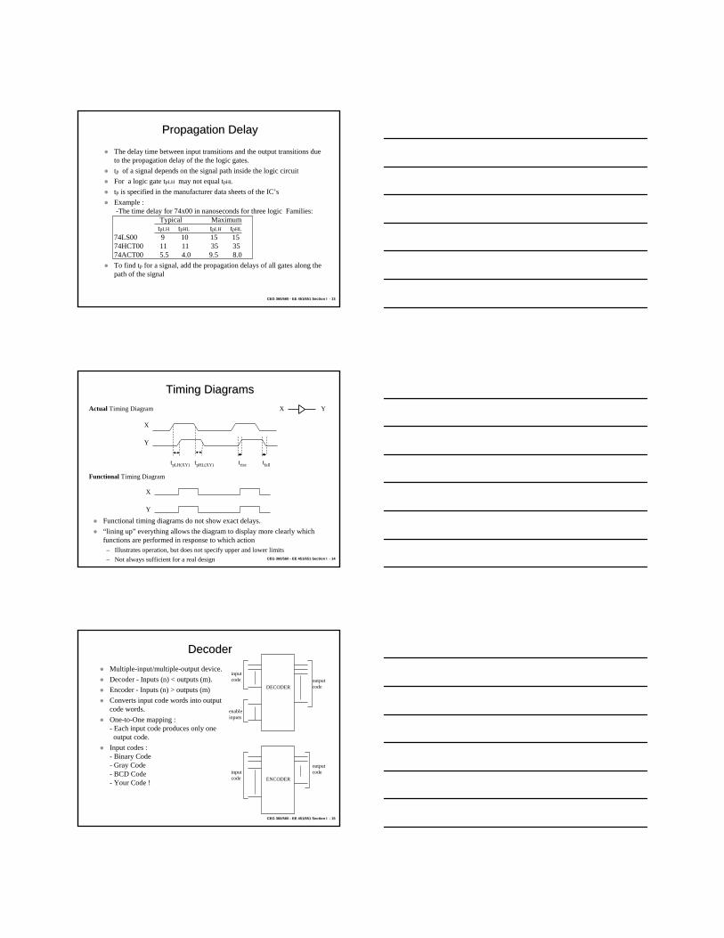
Types of Sequential LogicTypes of Sequential Logic
An Asynchronous Sequential Circuit uses ordinary gates and feedback loops to implement “memory” in a logic circuit.
– Meeting minimum pulse width requirements may be tricky
A Synchronous Sequential Circuit uses flip-flops (internally, an asynchronous sequential device) to form useful sequential logic functions or applications.
– The state variables and outputs of a synchronous system change with respect to a controlling clock signal
– Meeting minimum pulse width requirements is simplified by restating all timing constraints in terms of the clock signal
CEG 360/560 - EE 451/651 Section I - 35
Sequential Logic Definitions
Clock - the master timing element behind the state changes of most sequential circuits.
– a clock signal is active high if the state changes occur at the rising edge (for edge triggered devices) or in the logic 1 state (for pulse-triggered devices)
– active low if state changes occur at the falling edge or in the logic 0 state.Clock Period - time between successive transitions in the same directionClock Frequency - reciprocal of the clock periodClock Tick - the first edge or pulse in a clock period, or the period itselfDuty Cycle - the percentage of time that a clock is at its assertion level
T Q(t) Q(t+1)________________________________________
0 0 00 1 11 0 11 1 0
________________________________________
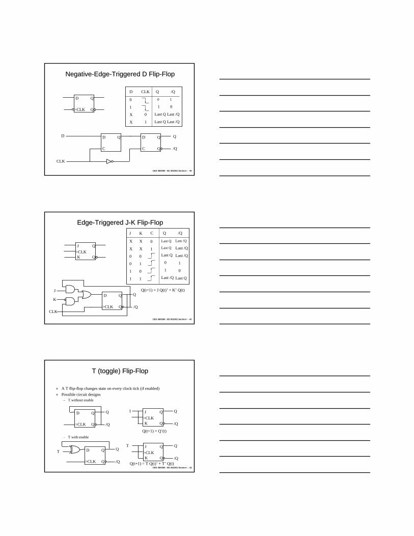
Characteristic Equation:
Q(t+1) = T Q’(t) + T’ Q(t)
Characteristic EquationsCharacteristic Equations
CEG 360/560 - EE 451/651 Section I - 47
Characteristic Equations Summary
Device Type Characteristic Equation___________________________________________________________________________________________________________________
S-R latch Q(t+1) = S + R’ Q(t)D latch Q(t+1) = D Edge-triggered D flip-flop Q(t+1) = DMaster/slave S-R flip-flop Q(t+1) = S + R’ Q(t)Master/slave J-K flip-flop Q(t+1) = J Q(t)’ + K’ Q(t)Edge-triggered J-K flip-flop Q(t+1) = J Q(t)’ + K’ Q(t)T flip-flop Q(t+1) = Q(t)’T flip-flop with enable Q(t+1) = T Q(t)’ + T’ Q(t)
CEG 360/560 - EE 451/651 Section I - 48
What Are FlipWhat Are Flip--flops?flops?
Common asynchronous (feedback) sequential circuitsLatch
– Single-bit storage (memory)– Changes state at any time due to input change– Must guarantee a minimum pulse width to avoid metastability– Fast and cheap (small # of transistors)– Often used in high speed microprocessor design
Flip-flop– Also single-bit storage– Changes state ONLY when a clock edge or pulse is applied– Uses setup and hold times before and after the clock pulse to avoid
metastability– Clocking simplifies the design process
CEG 360/560 - EE 451/651 Section I - 49
Combinationaltpd,min - minimum propagation delay, input to outputtpd,max - maximum propagation delay, input to output
Latch tpd,min - minimum propagation delay, input to outputtpd,max - maximum propagation delay, input to outputtw - minimum pulse width, input to input
Flip-fliptpd, min - minimum propagation delay, CLK to outputtpd, max - maximum propagation delay, CLK to output tsetup - required time of stable input before CLK, input before CLKthold - required time of stable input after CLK, input after CLK
FlipFlip--flop Timingflop Timing
J
K
Q
Q>CLK
tpd
tsetup, thold
CEG 360/560 - EE 451/651 Section I - 50
Asynchronous InputsAsynchronous Inputs
Most flip-flops have two asynchronous/direct inputsPreset and Reset (or Clear)Directly set or reset the /S-/R latchesOperate independent of clock
Good design practice dictates:– NEVER use asynchronous inputs for logic functions, only for system
initialization to a known stateWhy? Recall:
– Synchronous circuits: behavior of circuit depends on the value of the signals at discrete points in time, determined by a control signal (clock)
– Asynchronous circuits: behavior of circuit depends on the order in which the inputs signals change (changes can occur at any time)
CEG 360/560 - EE 451/651 Section I - 51
OutlineOutline
Review of Combinational Logic ConceptsWhat is Sequential Logic?
– Bi-stable Logic Elements and MetastabilityBasic Sequential Devices
– Flip-flops: Type, Function, and Structure– Characteristic Equations
The Clocked Synchronous State Machine (CSSM)– Analysis of State Machines
General structure, Analysis procedureCSSM Models: Mealy Vs. Moore
– Methods of RepresentationState tables and diagrams
– TimingCalculating Setup Time, Hold Times, and Maximum clock rate
CEG 360/560 - EE 451/651 Section I - 52
Clocked Synchronous State-machine Analysis
Analysis– How does a given circuit work? What does it do?– How do input sequences map to output sequences?
Clocked synchronous state-machine– Clocked: storage elements (flip-flops) use a clock input– Synchronous: all flip-flops use the same clock signal
State-machine types– Mealy Machine (most general type):
Next state = F ( current state, inputs ) Output = G ( current state, inputs )
– Moore Machine:Next state = F ( current state, inputs ) Output = G ( current state )
CEG 360/560 - EE 451/651 Section I - 53
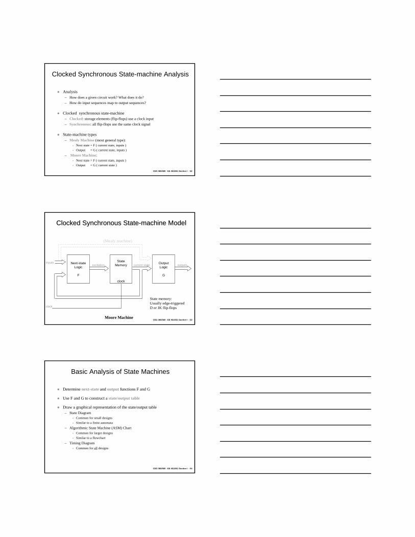
Clocked Synchronous StateClocked Synchronous State--machine Modelmachine Model
Next-stateLogic
F
StateMemory
clock
OutputLogic
G
excitationinputs
clock
current state outputs
(Mealy machine)
Moore Machine
State memory:Usually edge-triggeredD or JK flip-flops
CEG 360/560 - EE 451/651 Section I - 54
Basic Analysis of State Machines
Determine next-state and output functions F and G
Use F and G to construct a state/output table
Draw a graphical representation of the state/output table– State Diagram
Common for small designsSimilar to a finite automata
– Algorithmic State Machine (ASM) ChartCommon for larger designsSimilar to a flowchart
– Timing DiagramCommon for all designs
CEG 360/560 - EE 451/651 Section I - 55
Detailed Analysis of State Machines
Analyze the combinational logic to determine flip-flop input (excitation) equations:
– Di = Fi (Q(t), X(t))– The input to each flip-flop is based upon current state and primary inputs
Substitute excitation equations into flip-flop characteristic equations, giving transition equation:
– Qi(t+1) = Hi( Di )
Construct a state table from the transition equationsFind output equations:
– Z(t) = G (Q(t), X(t))– The primary outputs are based upon the current state and primary inputs– Add output values to the state table– Provide meaningful names for the states in state table, if possible– The graphical representation of state table is called a state diagram
Analyze timing requirements
CEG 360/560 - EE 451/651 Section I - 56
B1
0, 1
A0 1
B
1 / 1
0 / 1, 1 / 0
A
0
Moore
Mealy
State DiagramState Diagram
0/0
Format:Arc = input XNode = state/output Q
Format:Arc = input X / mealy output YNode = state
State
Output
Input
Basic Format:
CEG 360/560 - EE 451/651 Section I - 57
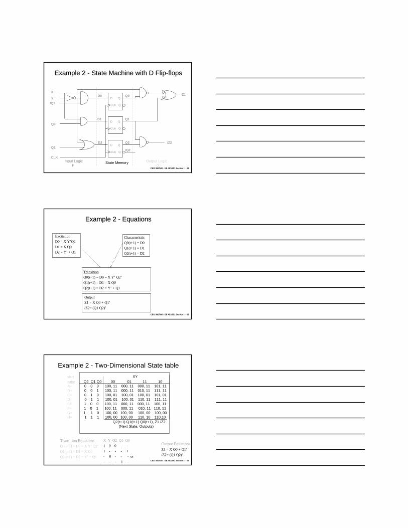
Example 1 Example 1 -- Circuit w/o Primary InputsCircuit w/o Primary Inputs
Transition EquationsQ0(t+1) = D0 = X Y’ Q2’Q1(t+1) = D1 = X Q0Q2(t+1) = D2 = Y’ + Q1
X Y Q2 Q1 Q01 0 0 - -1 - - - 1- 0 - - - or - - - 1 -
Output EquationsZ1 = X Q0 + Q1’/Z2= (Q1 Q2)’
CEG 360/560 - EE 451/651 Section I - 64
XYS 00 01 11 10 A E, 11 A, 11 A, 11 F, 11B E, 11 A, 11 C, 11 H, 11C E, 01 E, 01 E, 01 F, 01D E, 01 E, 01 G, 11 H, 11E E, 11 A, 11 A, 11 E, 11F E, 11 A, 11 C, 11 G, 11G E, 00 E, 00 E, 00 E, 00H E, 00 E, 00 G, 10 G,10
S(t+1), Z1 /Z2
Example 2 - Named State / Output table
CEG 360/560 - EE 451/651 Section I - 65
A
E
C
DH
B
F
G
Y (11) (11) X’ Y X Y (11)
X’ Y’(11)
X Y’(11)
X’Y’(11) XY’
(11)
XY’(01)
X’+Y(01)
Different formatArc: input expression (outputs) = expression (Z1 /Z2)
BAx y’ (11)
x’ y (10)
Also possible:Same transition,but different outputs
Example 2 - State Diagram
XY’(11)
X’(01)
XY(11)
Incomplete!
CEG 360/560 - EE 451/651 Section I - 66
Analysis of JAnalysis of J--K FlipK Flip--Flop State MachinesFlop State Machines
There are two excitation equations per flip-flop (J , K)
The characteristic equation : Q(t+1) = J·Q(t)’ + K’·Q(t)
Use the same analysis procedure shown previously
CEG 360/560 - EE 451/651 Section I - 67
Example 3 Example 3 -- State Machine with JState Machine with J--K FlipK Flip--flopsflops
Example 3 Example 3 -- Named State/Output TableNamed State/Output Table
XY
S 00 01 11 10
A B,0 B,0 C,0 C,0
B B,1 B,1 D,1 D,1
C D,0 D,0 A,1 C,1
D D,1 D,1 B,1 D,1S(t+1), Z
CEG 360/560 - EE 451/651 Section I - 71
A B
CD00,01,10
1
101
00,011
00,010
111
10,110
00,010
111
10,111
Arc Format:inputs xyoutput z
Example 3 Example 3 -- State DiagramState Diagram
CEG 360/560 - EE 451/651 Section I - 72
A B
CD(XY)’
1
XY’1
X’1
X’0
XY1
X0
X’0
XY1
X1
Arc Format:Transition Expression
output
Example 3 Example 3 -- State DiagramState Diagram
For each state/input combination there must be exactly one next-state (and output).
Mutual Exclusion: No more than one transition arc from any state can be satisfied byany input assignment
All Inclusion: At least one transition arc must exist from any state for any inputassignment
CEG 360/560 - EE 451/651 Section I - 73
Timing AnalysisTiming Analysis
All digital devices have associated propagation delays (min,max)Sequential devices have setup and hold times that must be satisfied to avoid metastable behaviorProviding a synchronous clock simplifies timing analysis
– All devices produce effects within a well-defined rangeAt what speeds will a device function?
– One transition per clock– What is the maximum clock rate?
Sequential devices require the following timing documentation:– Maximum propagation delay (clock to output)– Minimum propagation delay (clock to output)– Setup time (input before clock)– Hold time (input after clock)
CEG 360/560 - EE 451/651 Section I - 74
74LS74 Data Sheet Timing74LS74 Data Sheet Timing
Parameter Min Max UnitstW Pulse Width - Clock High 18 ns
- Preset Low 15 ns- Clear Low 15 ns
tSU Setup Time 20 nstH Hold Time 0 nsfMAX Max Clock Frequency 20 MHztPLH Prop Delay, Clock-to-Q 35 nstPLH Prop Delay, Preset-to-Q 35 nstPLH Prop Delay, Clear-to-Q 35 ns


![Digital Logic & Computer Design[Morris Mano]](https://static.documents.pub/doc/80x56/613cb742a3339922f86ee669/digital-logic-amp-computer-designmorris-mano.jpg)
