This section provides information on Avalon® Memory-Mapped (Avalon-MM) and Avalon Streaming (Avalon-ST) components that can be added to SOPC Builder systems. The components described in these chapters help you to create and optimize your SOPC Builder system. They are provided for free and can be used without a license in any design targeting an Altera device.
This chapter introduces Avalon® Memory-Mapped (Avalon-MM) bridges, and describes the Avalon-MM bridge components provided by Altera® for use in SOPC Builder systems.
You use bridges to control the topology of the generated SOPC Builder system. Bridges are not end-points for data, but rather affect the way data is transported between components. By inserting Avalon-MM bridges between masters and slaves, you control system topology, which in turn affects the interconnect that SOPC Builder generates. You can also use bridges to separate components in different clock domains and to implement clock domain crossing logic. Manual control of the interconnect can result in higher performance or lower logic utilization or both. Altera provides the following Avalon-MM bridges:
■ “Avalon-MM Pipeline Bridge” on page 11–7
■ “Clock Crossing Bridge” on page 11–10
■ “Avalon-MM DDR Memory Half-Rate Bridge” on page 11–18
f For additional information on using bridges to optimize and control the topology of SOPC Builder systems, refer to Avalon Memory-Mapped Design Optimizations in the Embedded Design Handbook.
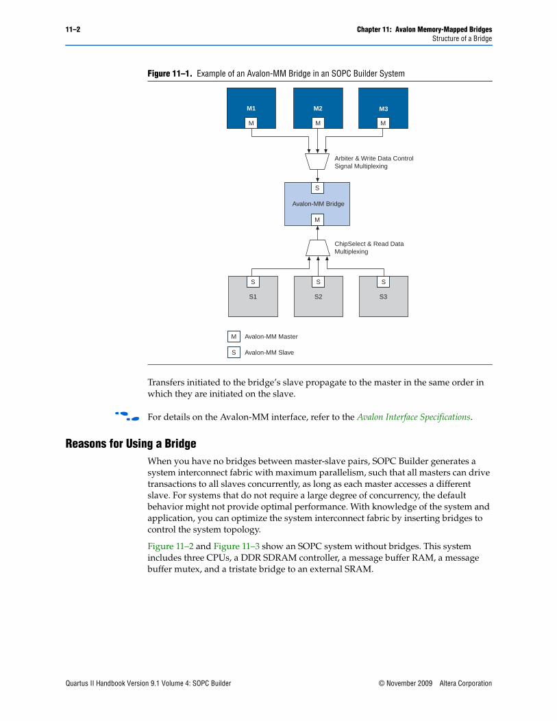
Structure of a BridgeA bridge has one Avalon-MM slave and one Avalon-MM master, as shown in Figure 11–1. In an SOPC Builder system, one or more masters connect to the bridge slave; in turn, the Avalon-MM bridge master connects to one or more slaves. In Figure 11–1, all three masters have logical connections to all three slaves, although physically each master only connects to the bridge.
Transfers initiated to the bridge’s slave propagate to the master in the same order in which they are initiated on the slave.
f For details on the Avalon-MM interface, refer to the Avalon Interface Specifications.
Reasons for Using a BridgeWhen you have no bridges between master-slave pairs, SOPC Builder generates a system interconnect fabric with maximum parallelism, such that all masters can drive transactions to all slaves concurrently, as long as each master accesses a different slave. For systems that do not require a large degree of concurrency, the default behavior might not provide optimal performance. With knowledge of the system and application, you can optimize the system interconnect fabric by inserting bridges to control the system topology.
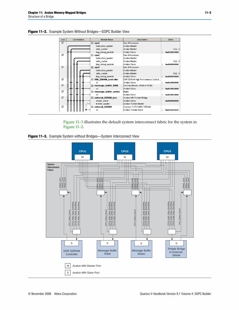
Figure 11–2 and Figure 11–3 show an SOPC system without bridges. This system includes three CPUs, a DDR SDRAM controller, a message buffer RAM, a message buffer mutex, and a tristate bridge to an external SRAM.
Figure 11–1. Example of an Avalon-MM Bridge in an SOPC Builder System
Figure 11–4 and Figure 11–5 show how inserting bridges can affect the generated logic. For example, if the DDR SDRAM controller can run at 166 MHz and the CPUs accessing it can run at 120 MHz, inserting an Avalon-MM clock-crossing bridge between the CPUs and the DDR SDRAM has the following benefits:
■ Allows the CPU and DDR interfaces to run at different frequencies.
■ Places system interconnect fabric for the arbitration logic and multiplexer for the DDR SDRAM controller in the slower clock domain.
■ Reduces the complexity of the interconnect logic in the faster domain, allowing the system to achieve a higher fMAX.
1 Inserting the clock-crossing bridge does increase read latency and may not be beneficial unless your system includes more devices that access the memory.
In the system illustrated in Figure 11–4, the message buffer RAM and message buffer mutex must respond quickly to the CPUs, but each response includes only a small amount of data. Placing an Avalon-MM pipeline bridge between the CPUs and the message buffers results in the following benefits:
■ Eliminates separate arbiter logic for the message buffer RAM and message buffer mutex, which reduces logic utilization and propagation delay, thus increasing the fMAX.
■ Reduces the overall size and complexity of the system interconnect fabric.
1 If an orange triangle appears next to an address in Figure 11–4, it indicates that the address is an offset value and is not the true value of the address in the address map.
Figure 11–5 shows the system interconnect fabric that SOPC Builder creates for the system in Figure 11–4. Figure 11–5 is the same system that is pictured in Figure 11–3 with bridges to control system topology.
Figure 11–4. Example SOPC System with Bridges—SOPC Builder View
Chapter 11: Avalon Memory-Mapped Bridges 11–5Structure of a Bridge
SOPC Builder follows several rules in constructing an address map for a system with Avalon-MM bridges:
1. The address span of each Avalon-MM slave is rounded up to the nearest power of two.
2. Each Avalon-MM slave connected to a bridge has an address relative to the base address of the bridge. This address must be a multiple of its span. (See Figure 11–6.)
3. In the example shown in Figure 11–6, if the address span of Slave 1 is 0x100 and the address span of Slave 2 is 0x200, Figure 11–7 illustrates the address span of the Avalon-MM bridge.
Figure 11–6. Avalon-MM Master and Slave Addresses
Avalon-MMBridgeSMaster1 M
Slave1S
Slave2S
S
M Avalon-MM Master Port
Avalon-MM Slave Port
Addr = 0x1000
Addr = 0x400
Addr = 0x100
Avalon-MM Master1 sees Slave1 at Addr = 0x1100Avalon-MM Master1 sees Slave2 at Addr = 0x1400
M
Figure 11–7. The Address Span of an Avalon-MM Bridge
Tools for Visualizing the Address MapThe Base Address column of the System Contents tab displays the base address offset of the Avalon-MM slave relative to the base address of the Avalon-MM bridge to which it is connected. You can see the absolute address map for each master in the system by clicking Address Map on the System Contents tab.
Differences between Avalon-MM Bridges and Avalon-MM Tristate BridgesYou use Avalon-MM bridges to control topology and separate clock domains for on-chip components. You use tristate bridges to connect to off-chip components and to share pins, decreasing the overall pin count of the device. Tristate bridges are transparent, meaning that they do not affect the addresses of the components to which they connect.
f For more information about the Avalon-MM tristate bridge, refer to the SOPC Builder Memory Subsystem Development Walkthrough chapter in volume 4 of the Quartus II Handbook.
Avalon-MM Pipeline BridgeThis section describes the hardware structure and functionality of the Avalon-MM pipeline bridge component.
Component OverviewThe Avalon-MM pipeline bridge inserts registers in the path between its master and slaves. In a given SOPC Builder system, if the critical register-to-register delay occurs in the system interconnect fabric, the pipeline bridge can help reduce this delay and improve system fMAX.
The bridge allows you to independently pipeline different groups of signals that can create a critical timing path in the interconnect:
■ Master-to-slave signals, such as address, write data, and control signals
■ Slave-to-master signals, such as read data
■ The waitrequest signal to the master
1 You can also use the Avalon-MM pipeline bridge to control topology without adding a pipeline stage. To instantiate a bridge that does not add any pipeline stages, simply do not select any of the Pipeline Options on the parameter page. For the system illustrated in Figure 11–5, a pipeline bridge that does not add a pipeline register stage is optimal because the CPUs benefit from minimal delay from the message buffer mutex and message buffer RAM.
c A pipeline bridge with no latency cannot be used with slaves that support pipelined reads. If a slave does not have read latency, you cannot connect it to a bridge with no pipeline stages, because the pipeline bridge slave port has a readdatavalid signal. Pipelined read components cannot have zero read latency. Some examples of 0 latency components available in SOPC Builder include the UART, Timer and SPI core. You are connecting a pipeline bridge to one of these components, increase the read latency from 0 to 1.
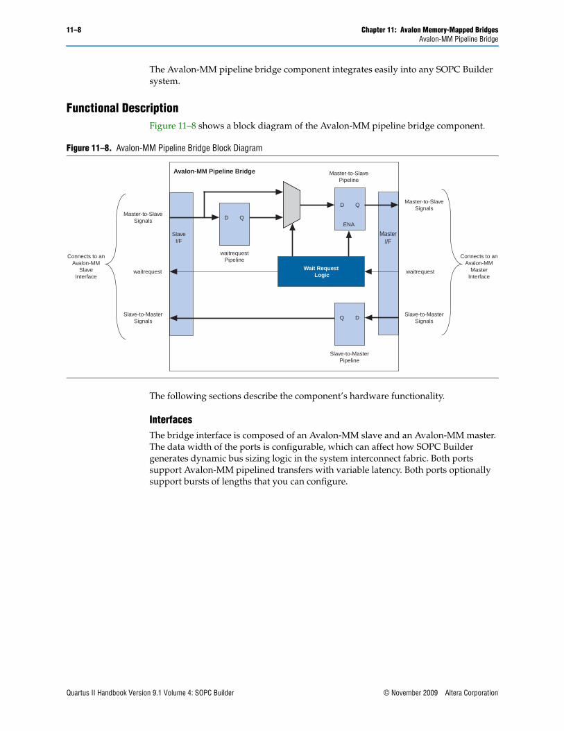
The Avalon-MM pipeline bridge component integrates easily into any SOPC Builder system.
Functional DescriptionFigure 11–8 shows a block diagram of the Avalon-MM pipeline bridge component.
The following sections describe the component’s hardware functionality.
InterfacesThe bridge interface is composed of an Avalon-MM slave and an Avalon-MM master. The data width of the ports is configurable, which can affect how SOPC Builder generates dynamic bus sizing logic in the system interconnect fabric. Both ports support Avalon-MM pipelined transfers with variable latency. Both ports optionally support bursts of lengths that you can configure.
Pipeline Stages and Effects on LatencyThe bridge provides three optional register stages to pipeline the following groups of signals.
■ Master-to-slave signals, including:
■ address
■ writedata
■ write
■ read
■ byteenable
■ chipselect
■ burstcount (optional)
■ Slave-to-master signals, including:
■ readdata
■ readdatavalid
■ The waitrequest signal to the master
When you include a register stage, it affects the timing and latency of transfers through the bridge, as follows:
■ The latency increases by one cycle in each direction.
■ Write transfers on the master side of the bridge are decoupled from write transfers on the slave side of the bridge because Avalon-MM write transfers do not require an acknowledge signal from the slave.
■ Including the waitrequest register stage increases the latency of master-to-slave signals by one additional cycle when the waitrequest signal is asserted.
Burst SupportThe bridge can support bursts with configurable maximum burst length. When configured to support bursts, the bridge propagates bursts between master-slave pairs, up to the maximum burst length. Not having burst support is equivalent to a maximum burst length of one. In this case, the system interconnect fabric automatically decomposes master-to-bridge bursts into a sequence of individual transfers.
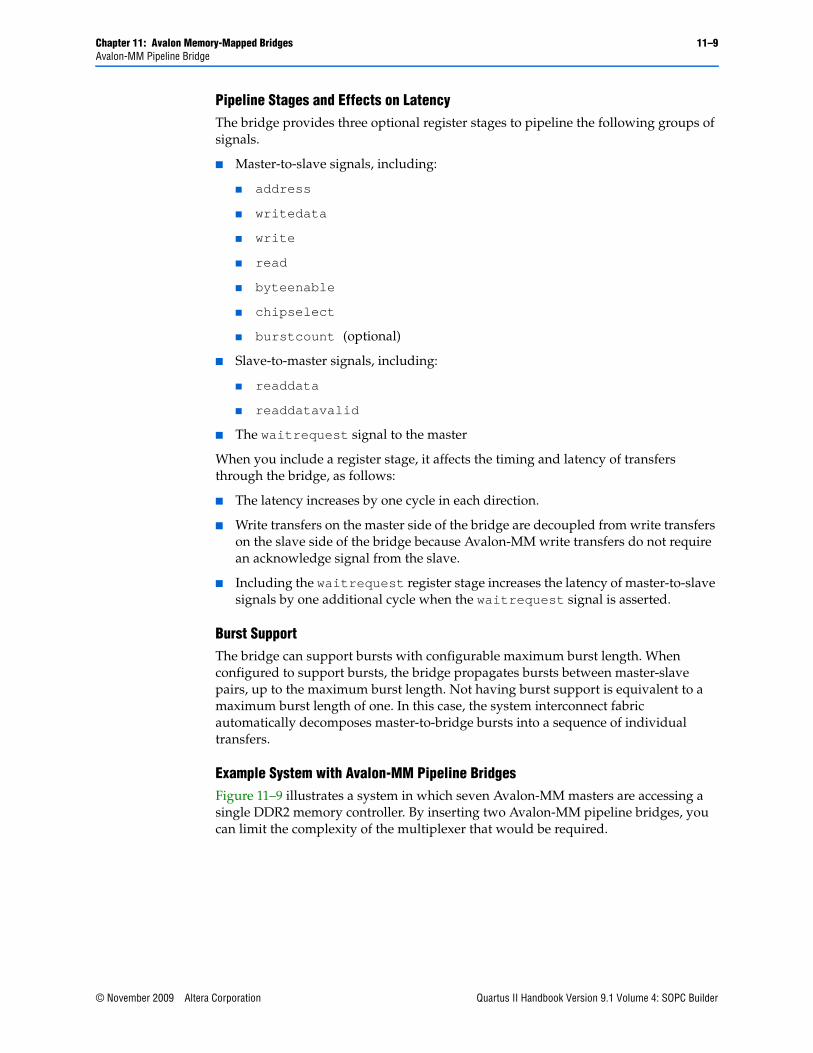
Example System with Avalon-MM Pipeline BridgesFigure 11–9 illustrates a system in which seven Avalon-MM masters are accessing a single DDR2 memory controller. By inserting two Avalon-MM pipeline bridges, you can limit the complexity of the multiplexer that would be required.
Clock Crossing BridgeThe Avalon-MM clock-crossing bridge allows you to connect Avalon-MM master and slaves that operate in different clock domains. Without a bridge, SOPC Builder automatically includes generic clock domain crossing (CDC) logic in the system interconnect fabric, but it does not provide optimal performance for high-throughput applications. Because the clock-crossing bridge includes a buffering mechanism, you can pipeline multiple read and write transfers. After an initial penalty for the first read or write, there is no additional latency penalty for pending reads and writes, increasing throughput at the expense primarily of on-chip memory. The clock-crossing bridge has parameterizeable FIFOs for master-to-slave and slave-to-master signals, and allows burst transfers across clock domains.
The Avalon-MM clock-crossing bridge component is SOPC Builder-ready and integrates easily into any SOPC Builder-generated system.
Choosing Clock Crossing MethodologyWhen determining clock frequencies for your components, you should also consider the impact on the latency that transferring data across clock domains can cause. Whether you use a clock-crossing bridge or rely on the clock domain adapter created automatically by SOPC Builder, additional latency occurs. You should also consider the resource usage and throughput capabilities of each solution.
Figure 11–9. Seven Avalon-MM Masters Accessing One Avalon-MM Slave
If you rely on the automatically generated clock crossing adapter to connect master and slave ports driven by separate clock inputs, there is a fixed latency penalty associated to each transfer. Each transfer becomes blocking, meaning that while one transfer is underway another cannot begin until the first completes. For this reason, you should not connect high-speed, pipelined components such as SDRAM memory to a master on a different clock domain without using a clock-crossing bridge between them. The clock crossing bridge, on the other hand, can queue multiple transfers, so that even though the latency increases, the throughput does not decrease.
Because a clock crossing adapter is generated for every master and slave pair, you should use a clock crossing bridge if your design contains multiple master and slave pairs operating in different clock domains. Alternatively, if your design uses a large amount of on-chip memory, you may need to use a clock domain adapter, because the clock-crossing bridge uses on-chip memory resources for buffering.
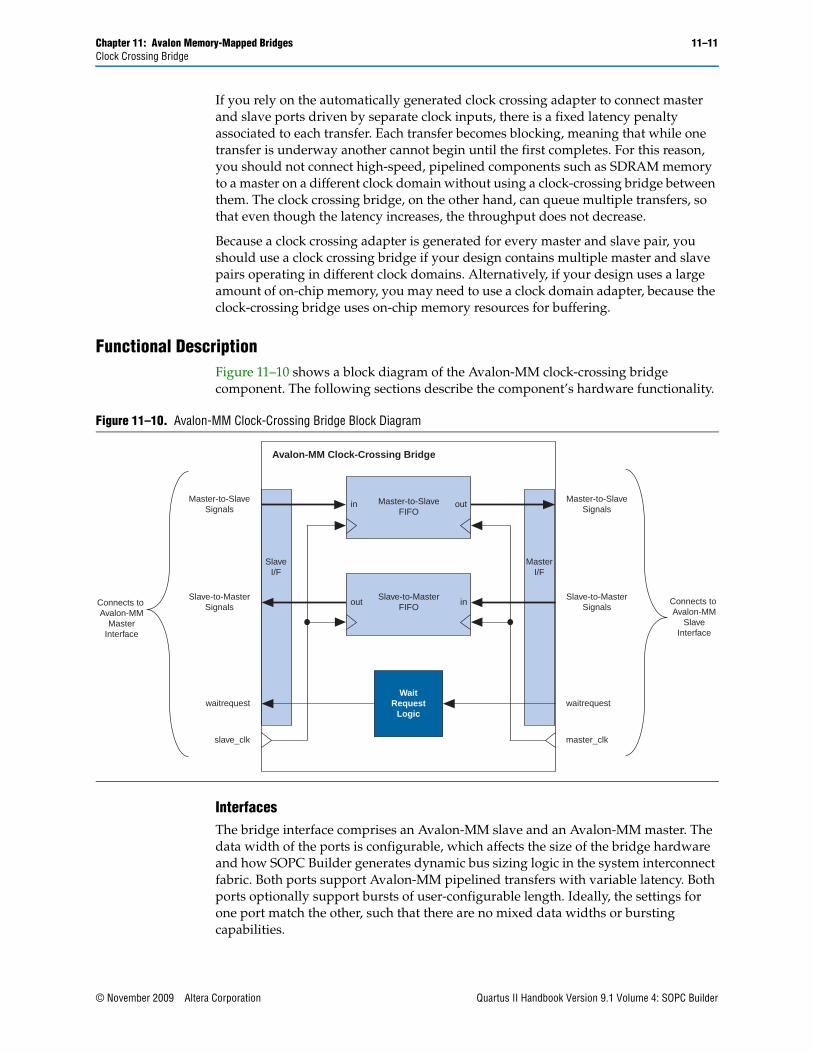
Functional DescriptionFigure 11–10 shows a block diagram of the Avalon-MM clock-crossing bridge component. The following sections describe the component’s hardware functionality.
InterfacesThe bridge interface comprises an Avalon-MM slave and an Avalon-MM master. The data width of the ports is configurable, which affects the size of the bridge hardware and how SOPC Builder generates dynamic bus sizing logic in the system interconnect fabric. Both ports support Avalon-MM pipelined transfers with variable latency. Both ports optionally support bursts of user-configurable length. Ideally, the settings for one port match the other, such that there are no mixed data widths or bursting capabilities.
Clock Crossing Bridge and FIFOsTwo FIFOs in the bridge transport address, data, and control signals across the clock domains. One FIFO captures data and controls traveling in the master-to-slave direction, and the other FIFO captures data in the slave-to-master direction. Clock crossing logic surrounding the FIFOs coordinates the details of passing data across the clock-domain boundaries and ensures that the FIFOs do not overflow or underflow.
The signals that pass through the master-to-slave FIFO include:
■ writedata
■ address
■ read
■ write
■ byteenable
■ burstcount, when bursting is enabled
The signals that pass through the slave-to-master FIFO include:
■ readdata
■ readdatavalid
You can configure the depth of each FIFO. Because there are more signals traveling in the master-to-slave direction, changing the depth of the master-to-slave FIFO has a greater impact on the memory utilization of the bridge.
For read transfers across the bridge, the FIFOs in both directions incur latency for data to return from the slave. To avoid paying a latency penalty for each transfer, the master can issue multiple reads that are queued in the FIFO. The slave of the bridge asserts readdatavalid when it drives valid data and asserts waitrequest when it is not ready to accept more reads.
For write transfers, the master-to-slave FIFO causes a delay between the master-to-bridge transfers and the corresponding bridge-to-slave transfers. Because Avalon-MM write transfers do not require an acknowledge from the slave, multiple write transfers from master-to-bridge might complete by the time the bridge initiates the corresponding bridge-to-slave transfers.
Burst SupportThe bridge optionally supports bursts with configurable maximum burst length. When configured to support bursts, the bridge propagates bursts between master-slave pairs, up to the maximum burst length. Not having burst support is equivalent to a maximum burst length of one. In this case, the system interconnect fabric automatically breaks master-to-bridge bursts into a sequence of individual transfers.
When you configure the bridge to support bursts, you must configure the slave-to-master FIFO depth deeply enough to capture all burst read data without overflowing. The masters connected to the bridge could potentially fill the master-to-slave FIFO with read burst requests; therefore, the minimum slave-to-master FIFO depth is described by equation given in Example 11–1.
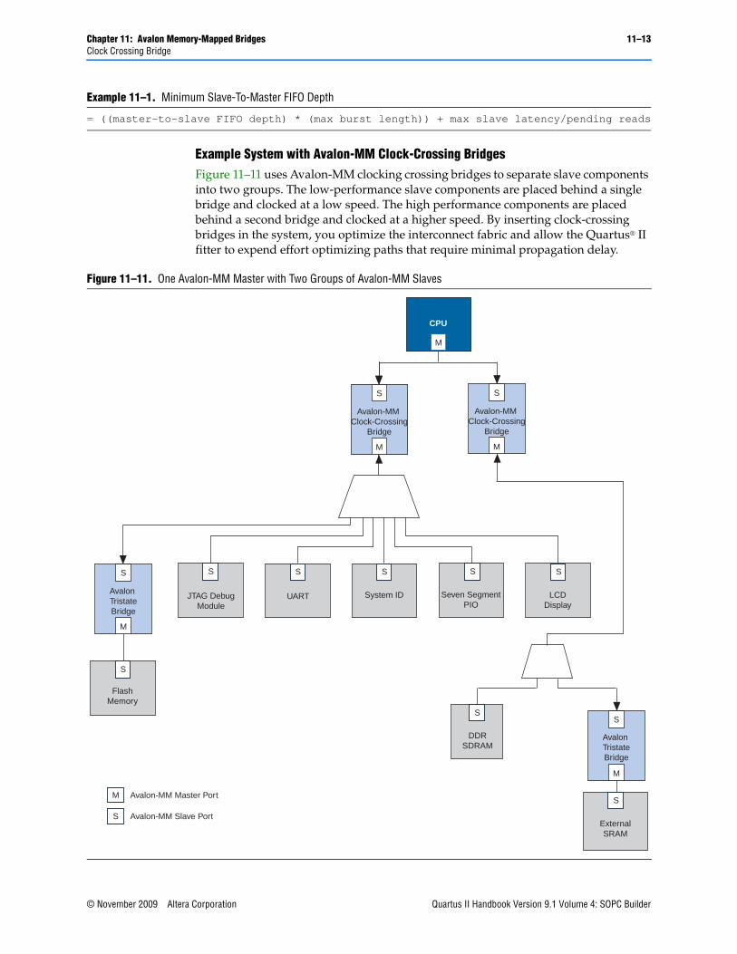
Example System with Avalon-MM Clock-Crossing BridgesFigure 11–11 uses Avalon-MM clocking crossing bridges to separate slave components into two groups. The low-performance slave components are placed behind a single bridge and clocked at a low speed. The high performance components are placed behind a second bridge and clocked at a higher speed. By inserting clock-crossing bridges in the system, you optimize the interconnect fabric and allow the Quartus® II fitter to expend effort optimizing paths that require minimal propagation delay.
Instantiating the Avalon-MM Clock-Crossing Bridge in SOPC BuilderTable 11–1 describes the options available on the Parameter Settings page of the MegaWizardTM interface.
FIFO depth 8, 16, 32 Determines the depth of the FIFO.
Construct FIFO with registers instead of memory blocks
On/Off When you turn on this option, the FIFO uses registers as storage instead of embedded memory blocks. This can considerably increase the size of the bridge hardware and lower the fMAX.
Slave-to-master FIFO
FIFO depth 8, 16, 32, 64, 128, 256, 512, 1024
Determines the depth of the FIFO.
Construct FIFO with registers instead of memory blocks
On/Off When you turn on this option, the FIFO uses registers as storage instead of embedded memory blocks. This can considerably increase the size of the bridge hardware and lower the fMAX.
Common options
Data width 8, 16, 32, 64, 128, 256,512, 1024
Determines the data width of the interfaces on the bridge, and affects the size of both FIFOs. For the highest bandwidth, set Data width to be as wide as the widest master connected to the bridge.
Slave domain synchronizer length
2–8 The number of pipeline stages in the clock crossing logic in the issuing master to target slave direction. Increasing this value leads to a larger meantime between failures (MTBF). You can determine the MTBF for a given design can be determined by running a TimeQuest timing analysis.
Master domain synchronizer length
2–8 The number of pipeline stages in the clock crossing logic in the issuing master to target slave direction. Increasing this value leads to a larger meantime between failures (MTBF). You can determine the MTBF for a given design can be determined by running a TimeQuest timing analysis.
Burst settings
Allow bursts On/Off Includes logic for the bridge’s master and slaves to support bursts. You can use this option to restrict the minimum depth for the slave-to-master FIFO.
Clock Domain Crossing LogicSOPC Builder generates CDC logic that hides the details of interfacing components operating in different clock domains. The system interconnect fabric upholds the Avalon-MM protocol with each port independently, and therefore masters do not need to incorporate clock adapters in order to interface to slaves on a different domain. The system interconnect fabric logic propagates transfers across clock domain boundaries automatically.
The clock-domain adapters in the system interconnect fabric provide the following benefits that simplify system design efforts:
■ Allow component interfaces to operate at different clock frequencies.
■ Eliminate the need to design CDC hardware.
■ Allow each Avalon-MM port to operate in only one clock domain, which reduces design complexity of components.
■ Enable masters to access any slave without communication with the slave clock domain.
■ Allow you to focus performance optimization efforts only on components that require fast clock speed.
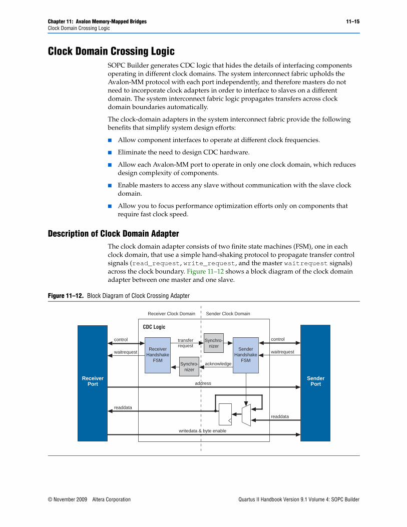
Description of Clock Domain AdapterThe clock domain adapter consists of two finite state machines (FSM), one in each clock domain, that use a simple hand-shaking protocol to propagate transfer control signals (read_request, write_request, and the master waitrequest signals) across the clock boundary. Figure 11–12 shows a block diagram of the clock domain adapter between one master and one slave.
Figure 11–12. Block Diagram of Clock Crossing Adapter
The synchronizer blocks in Figure 11–12 use multiple stages of flipflops to eliminate the propagation of metastable events on the control signals that enter the handshake FSMs.
The CDC logic works with any clock ratio. Altera tests the CDC logic extensively on a variety of system architectures, both in simulation and in hardware, to ensure that the logic functions correctly.
The typical sequence of events for a transfer across the CDC logic is described as follows:
1. Master asserts address, data, and control signals.
2. The master handshake FSM captures the control signals, and immediately forces the master to wait.
1 The FSM uses only the control signals, not address and data. For example, the master simply holds the address signal constant until the slave side has safely captured it.
3. Master handshake FSM initiates a transfer request to the slave handshake FSM.
4. The transfer request is synchronized to the slave clock domain.
5. The slave handshake FSM processes the request, performing the requested transfer with the slave.
6. When the slave transfer completes, the slave handshake FSM sends an acknowledge back to the master handshake FSM.
7. The acknowledge is synchronized back to the master clock domain.
8. The master handshake FSM completes the transaction by releasing the master from the wait condition.
Transfers proceed as normal on the slave and the master side, without a special protocol to handle crossing clock domains. From the perspective of a slave, there is nothing different about a transfer initiated by a master in a different clock domain. From the perspective of a master, a transfer across clock domains simply requires extra clock cycles. Similar to other transfer delay cases (for example, arbitration delay or wait states on the slave side), the system interconnect fabric simply forces the master to wait until the transfer terminates. As a result, pipeline master ports do not benefit from pipelining when performing transfers to a different clock domain.
Location of Clock Domain AdapterYou can use the clock crossing bridge described in the following paragraphs for higher throughput clock crossing, at the expense of memory resources.
SOPC Builder automatically determines where to insert the CDC logic, based on the system contents and the connections between components. SOPC Builder places CDC logic to maintain the highest transfer rate for all components. SOPC Builder evaluates the need for CDC logic for each master and slave pair independently, and generates CDC logic wherever necessary.
Duration of Transfers Crossing Clock DomainsCDC logic extends the duration of master transfers across clock domain boundaries. In the worst case which is for reads, each transfer is extended by five master clock cycles and five slave clock cycles. Assuming the default value of 2 for the Master domain synchronizer length and the Slave domain synchronizer length, the components of this delay are the following:
■ Four additional master clock cycles, due to the master-side clock synchronizer
■ Four additional slave clock cycles, due to the slave-side clock synchronizer
■ One additional clock in each direction, due to potential metastable events as the control signals cross clock domains
1 Systems that require a higher performance clock should use the Avalon-MM clock crossing bridge instead of the automatically inserted CDC logic. The clock crossing bridge includes a buffering mechanism, so that multiple reads and writes can be pipelined. After paying the initial penalty for the first read or write, there is no additional latency penalty for pending reads and writes, increasing throughput by up to four times, at the expense of added logic resources.
f For more information, refer to the System Interconnect Fabric for Streaming Interfaces chapter in volume 4 of the Quartus II Handbook and Avalon Memory-Mapped Design Optimizations in the Embedded Design Handbook.
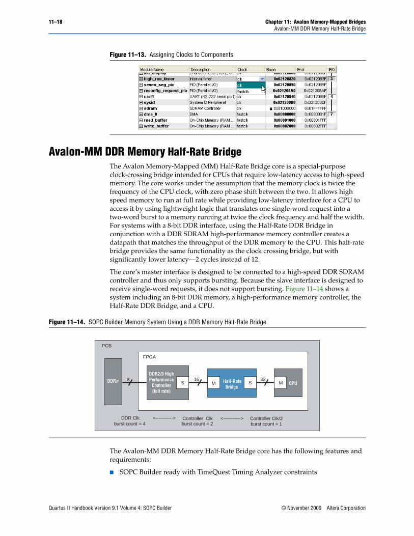
Implementing Multiple Clock Domains in SOPC BuilderYou specify the clock domains used by your system on the System Contents tab of SOPC Builder. You define the input clocks to the system with the Clock Settings table. Clock sources can be driven by external input signals to the SOPC Builder system or by PLLs inside the SOPC Builder system. Clock domains are differentiated based on the name of the clock. You may create multiple asynchronous clocks with the same frequency.
To specify which clock drives which components you must display the Clock column in the System Contents tab. By default, clock names are not displayed. To display clock names in the Module Name column and the clocks in the Clock column in the System Contents tab, right-click in the Module Name column and click Show All. To connect a clock to follow these steps.
1. Click in the Clock column next to the clock port. A list of available clock signals appears.
2. Select the appropriate signal from the list of available clocks. Figure 11–13 illustrates this step.
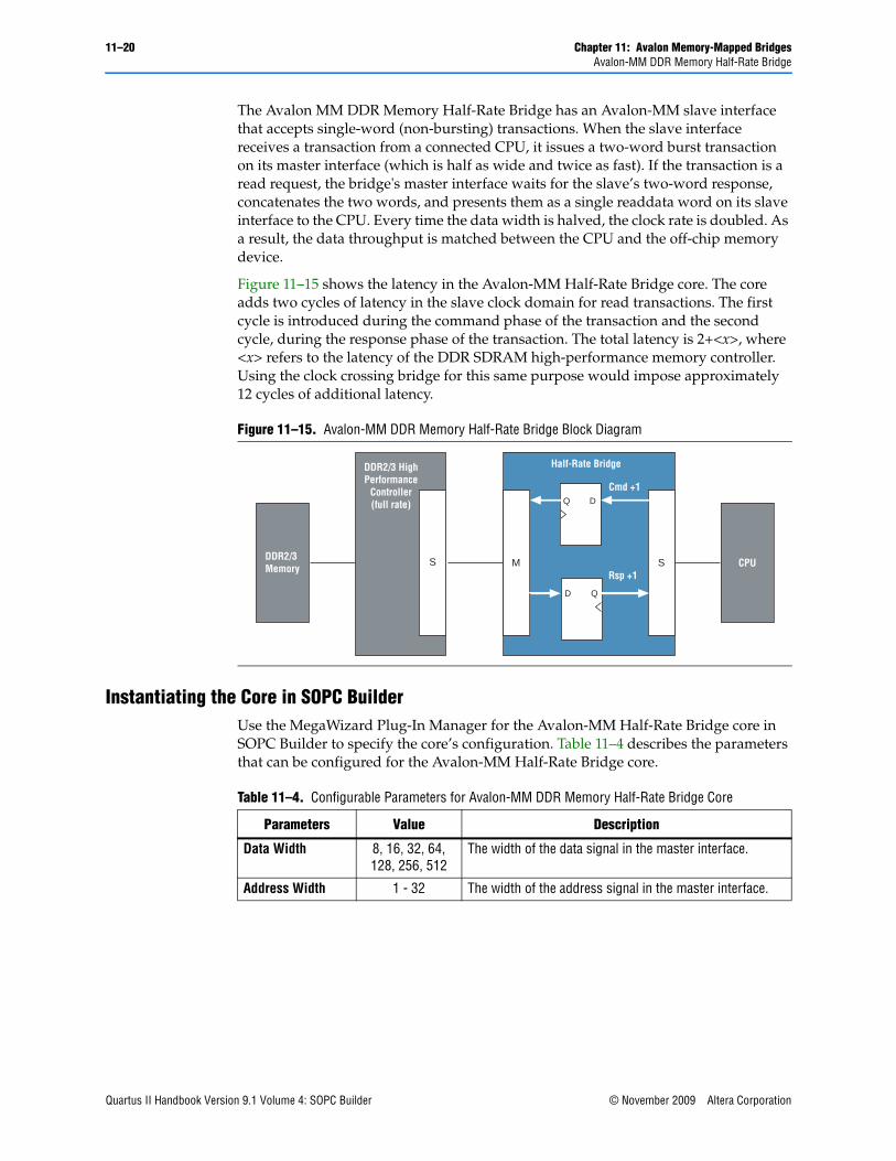
Avalon-MM DDR Memory Half-Rate BridgeThe Avalon Memory-Mapped (MM) Half-Rate Bridge core is a special-purpose clock-crossing bridge intended for CPUs that require low-latency access to high-speed memory. The core works under the assumption that the memory clock is twice the frequency of the CPU clock, with zero phase shift between the two. It allows high speed memory to run at full rate while providing low-latency interface for a CPU to access it by using lightweight logic that translates one single-word request into a two-word burst to a memory running at twice the clock frequency and half the width. For systems with a 8-bit DDR interface, using the Half-Rate DDR Bridge in conjunction with a DDR SDRAM high-performance memory controller creates a datapath that matches the throughput of the DDR memory to the CPU. This half-rate bridge provides the same functionality as the clock crossing bridge, but with significantly lower latency—2 cycles instead of 12.
The core’s master interface is designed to be connected to a high-speed DDR SDRAM controller and thus only supports bursting. Because the slave interface is designed to receive single-word requests, it does not support bursting. Figure 11–14 shows a system including an 8-bit DDR memory, a high-performance memory controller, the Half-Rate DDR Bridge, and a CPU.
The Avalon-MM DDR Memory Half-Rate Bridge core has the following features and requirements:
■ SOPC Builder ready with TimeQuest Timing Analyzer constraints
Figure 11–13. Assigning Clocks to Components
Figure 11–14. SOPC Builder Memory System Using a DDR Memory Half-Rate Bridge
■ Requires master clock and slave clock to be synchronous
■ Handles different bus sizes between CPU and memory
■ Requires the frequency of the master clock to be double of the slave clock
■ Has configurable address and data port widths in the master interface
Resource Usage and PerformanceThis section lists the resource usage and performance data for supported devices when operating the Half-Rate Bridge with a full-rate DDR SDRAM high-performance memory controller.
Using the Half-Rate Bridge with a full-rate DDR SDRAM high-performance memory controller results an average of 48% performance improvement over a system using a half-rate DDR SDRAM high-performance memory controller in a series of embedded applications. The performance improvement is 62.2% based on the Dhrystone benchmark, and 87.7% when accessing memory bypassing the cache. For memory systems that use the Half-Rate bridge in conjunction with DDR2/3 High Performance Controller, the data throughput is the same on the Half-Rate Bridge master and slave interfaces. The decrease in memory latency on the Half-Rate Bridge slave interface results in higher performance for the processor.
Table 11–2 shows the resource usage for Stratix® II and Stratix III devices in version 9.1 of the Quartus II software with a data width of 16 bits, an address span of 24 bits.
Table 11–3 lists the resource usage for a Cyclone® III device.
Functional DescriptionThe Avalon MM DDR Memory Half Rate Bridge works under two constraints:
■ Its memory-side master has a clock frequency that is synchronous (zero phase shift) to, and twice the frequency of, the CPU-side slave.
■ Its memory-side master is half as wide as its CPU-side slave.
The bridge leverages these two constraints to provide lightweight, low-latency clock-crossing logic between the CPU and the memory. These constraints are in contrast with the Avalon-MM Clock-Crossing Bridge, which makes no assumptions about the frequency/phase relationship between the master- and slave-side clocks, and provides higher-latency logic that fully-synchronizes all signals that pass between the two domains.
Table 11–2. Resource Utilization Data for Stratix II and Stratix III Devices
Device FamilyCombinational
ALUTs ALMs Logic RegisterEmbeddedMemory
Stratix II 61 134 153 0
Stratix III 60 138 153 0
Table 11–3. Resource Utilization Data for Cyclone III Devices
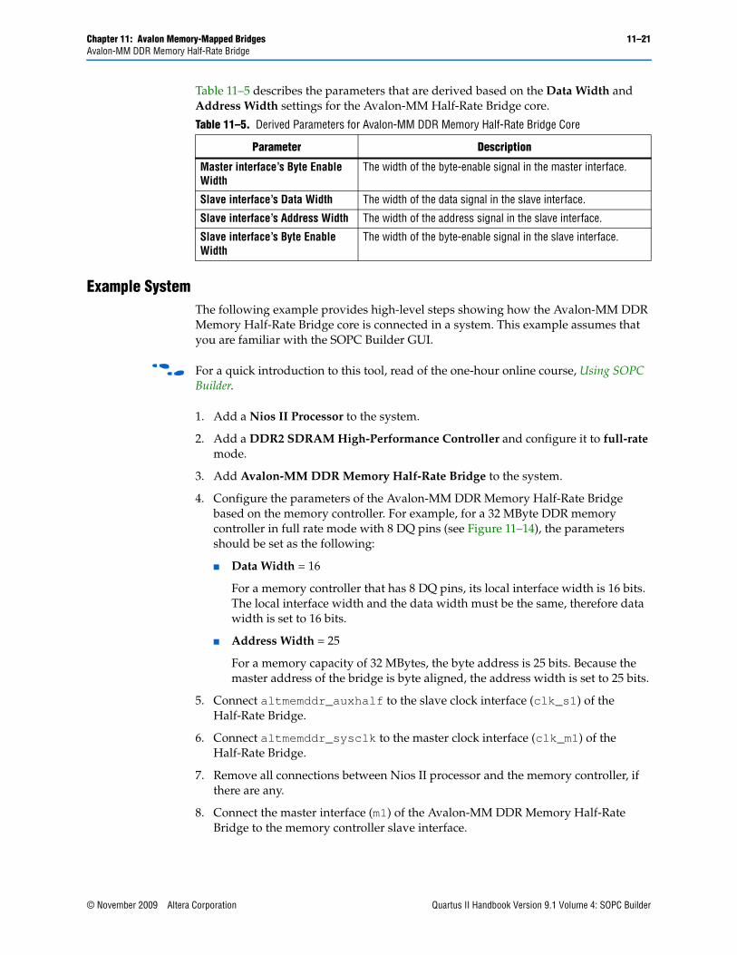
The Avalon MM DDR Memory Half-Rate Bridge has an Avalon-MM slave interface that accepts single-word (non-bursting) transactions. When the slave interface receives a transaction from a connected CPU, it issues a two-word burst transaction on its master interface (which is half as wide and twice as fast). If the transaction is a read request, the bridge's master interface waits for the slave’s two-word response, concatenates the two words, and presents them as a single readdata word on its slave interface to the CPU. Every time the data width is halved, the clock rate is doubled. As a result, the data throughput is matched between the CPU and the off-chip memory device.
Figure 11–15 shows the latency in the Avalon-MM Half-Rate Bridge core. The core adds two cycles of latency in the slave clock domain for read transactions. The first cycle is introduced during the command phase of the transaction and the second cycle, during the response phase of the transaction. The total latency is 2+<x>, where <x> refers to the latency of the DDR SDRAM high-performance memory controller. Using the clock crossing bridge for this same purpose would impose approximately 12 cycles of additional latency.
Instantiating the Core in SOPC BuilderUse the MegaWizard Plug-In Manager for the Avalon-MM Half-Rate Bridge core in SOPC Builder to specify the core’s configuration. Table 11–4 describes the parameters that can be configured for the Avalon-MM Half-Rate Bridge core.
Table 11–5 describes the parameters that are derived based on the Data Width and Address Width settings for the Avalon-MM Half-Rate Bridge core.
Example SystemThe following example provides high-level steps showing how the Avalon-MM DDR Memory Half-Rate Bridge core is connected in a system. This example assumes that you are familiar with the SOPC Builder GUI.
f For a quick introduction to this tool, read of the one-hour online course, Using SOPC Builder.
1. Add a Nios II Processor to the system.
2. Add a DDR2 SDRAM High-Performance Controller and configure it to full-rate mode.
3. Add Avalon-MM DDR Memory Half-Rate Bridge to the system.
4. Configure the parameters of the Avalon-MM DDR Memory Half-Rate Bridge based on the memory controller. For example, for a 32 MByte DDR memory controller in full rate mode with 8 DQ pins (see Figure 11–14), the parameters should be set as the following:
■ Data Width = 16
For a memory controller that has 8 DQ pins, its local interface width is 16 bits. The local interface width and the data width must be the same, therefore data width is set to 16 bits.
■ Address Width = 25
For a memory capacity of 32 MBytes, the byte address is 25 bits. Because the master address of the bridge is byte aligned, the address width is set to 25 bits.
5. Connect altmemddr_auxhalf to the slave clock interface (clk_s1) of the Half-Rate Bridge.
6. Connect altmemddr_sysclk to the master clock interface (clk_m1) of the Half-Rate Bridge.
7. Remove all connections between Nios II processor and the memory controller, if there are any.
8. Connect the master interface (m1) of the Avalon-MM DDR Memory Half-Rate Bridge to the memory controller slave interface.
9. Connect the slave interface (s1) of the Avalon-MM DDR Memory Half-Rate Bridge to the Nios II processor data_master interface.
10. Connect altmemddr_auxhalf to Nios II processor clock interface.
Device SupportAltera device support for the bridge components is listed in Table 11–6.
Hardware Simulation ConsiderationsThe bridge components do not provide a simulation testbench for simulating a stand-alone instance of the component. However, you can use the standard SOPC Builder simulation flow to simulate the component design files inside an SOPC Builder system.
Software Programming ModelThe bridge components do not have any user-visible control or status registers. Therefore, software cannot control or configure any aspect of the bridges during run-time. The bridges cannot generate interrupts.
Table 11–6. Device Family Support
Device FamilyAvalon-MM Pipeline
Bridge Support
Avalon-MM Clock-Crossing Bridge
SupportAvalon-MM Half-Rate
Bridge
Arria® GX Full Full Full
Arria II GX Full Full Full
Stratix® Full Full Full
Stratix II Full Full Full
Stratix II GX Full Full Full
Stratix III Full Full Full
Stratix IV Full Full Full
Cyclone® Full Full Full
Cyclone II Full Full Full
Cyclone III Full Full Full
Hardcopy® Full Full Full
HardCopy II Full Full Full
HardCopy III Full Full Full
MAX® Full No support No support
MAX II Full No support No support
Chapter 11: Avalon Memory-Mapped Bridges 11–23Document Revision History
Document Revision HistoryTable 11–7 shows the revision history for this chapter.
Table 11–7. Document Revision History
Date and Document Version Changes Made Summary of Changes
November 2009, v9.1.0 ■ Added configuration information for resource utilization of half-rate bridge.
—
March 2009, v9.0.0 ■ Added information for synchronization when crossing clock domains.
New information to allow user control of metastability.
November 2008 v8.1 ■ Clarified connection of clock signals.
■ Added section describing half-rate bridge.
■ Changed page size to 8.5 x 11 inches.
—
May 2008 v8.0 ■ Chapter renumbered from 10 to 11.
■ Corrected Figure 11–4 to show correct connectivity between masters and bridges. Show JTAG debug modules for each CPU behind pipeline bridge.
■ Deleted references to Avalon Memory-Mapped and Streaming Interface Specifications and replaced with new Avalon Interface Specifications.
■ Moved clock crossing bridge section from Chapter 2 to this chapter.
■ Added note after Figure 10-4.
—
October 2007 v7.2.0 Moved discussion of clock-crossing bridge from this chapter to chapter 2.
—
May 2007, v7.1.0
Initial release of the document. The Avalon-MM Pipeline Bridge and Avalon-MM Clock-Crossing Bridge are new components provided in the Quartus II software v7.1 release.
Avalon® Streaming (Avalon-ST) interconnect components facilitate the design of high-speed, low-latency datapaths for the system-on-a-programmable-chip (SOPC) environment. Interconnect components in SOPC Builder act as a part of the system interconnect fabric. They are not end points, but adapters that allow you to connect different, but compatible, streaming interfaces. You use Avalon-ST interconnect components to connect cores that send and receive high-bandwidth data, including multiplexed streams, packets, cells, time-division multiplexed (TDM) frames, and digital signal processor (DSP) data.
The interconnect components that you add to an SOPC Builder system insert logic between a source and sink interface, enabling that interface to operate correctly. This chapter describes four Avalon-ST interconnect components, also called adapters:
■ “Timing Adapter” on page 12–3—adapts between sinks and sources that have different characteristics, such as ready latencies.
■ “Data Format Adapter” on page 12–6—adapts source and sink interfaces that have different data widths.
■ “Channel Adapter” on page 12–8—adapts source and sink interfaces that have different settings for the channel signal.
■ “Error Adapter” on page 12–9—ensures that per-bit error information recorded at the source is correctly transferred to the sink
All of these interconnect components adapt initially incompatible Avalon-ST source and sink interfaces so that they function correctly, facilitating the development of high-speed, low-latency datapaths.
Interconnect Component UsageInterconnect components can adapt the data or control signals of the Avalon-ST interface. Typical adaptations to control signals include:
■ Adding pipeline stages to adjust the timing of the ready signal
■ Tying signals that are not used by either the source or sink to 0 or 1
Typical adaptations to data signals include:
■ Changing the number of symbols (words) that are driven per cycle
■ Changing the number of channels driven
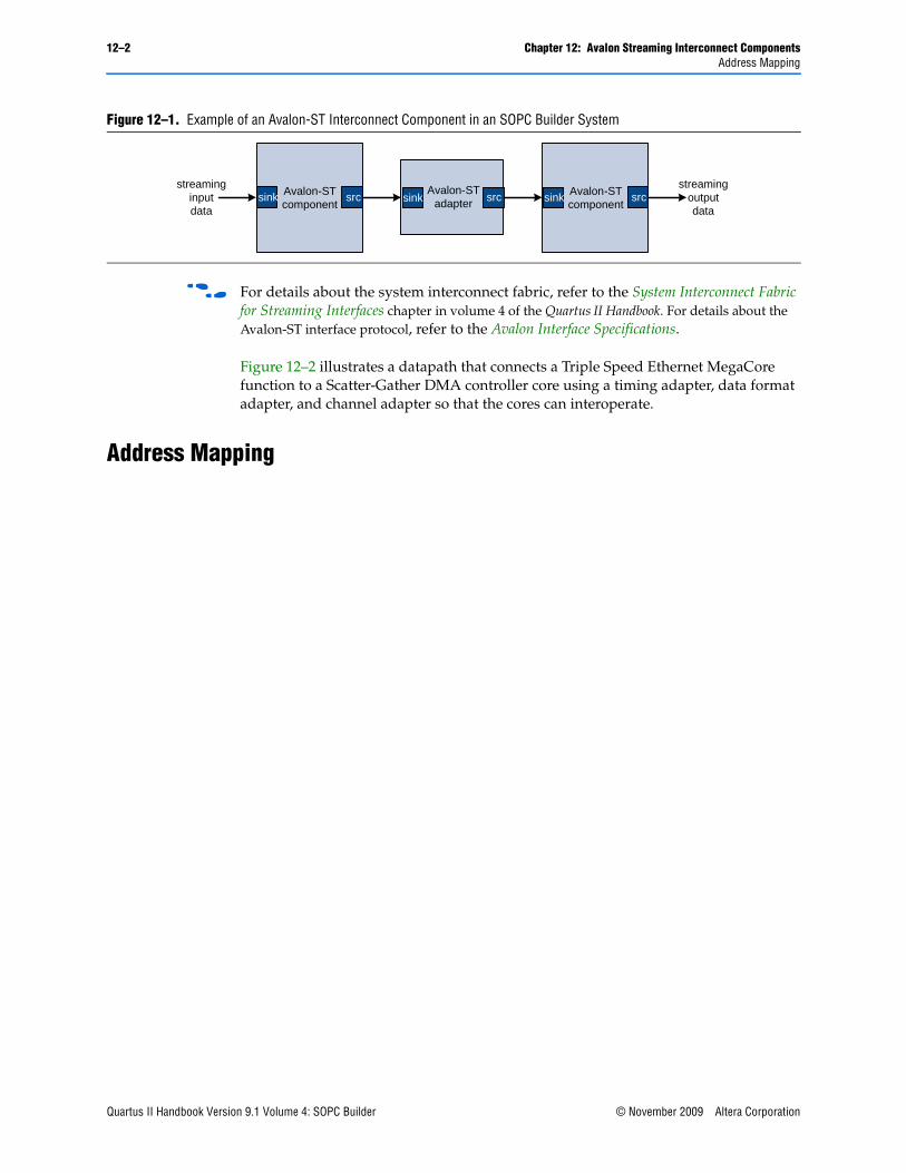
When the interconnect component adapts the data interface, it has one Avalon-ST sink interface and one Avalon-ST source interface, as shown in Figure 12–1. You configure the adapter components manually, using SOPC Builder. In contrast to the Avalon-MM interface, which allows you to create various topologies with a number of different master and slave components, you always use the Avalon-ST interconnect components to adapt point-to-point connections between streaming cores.
f For details about the system interconnect fabric, refer to the System Interconnect Fabric for Streaming Interfaces chapter in volume 4 of the Quartus II Handbook. For details about the Avalon-ST interface protocol, refer to the Avalon Interface Specifications.
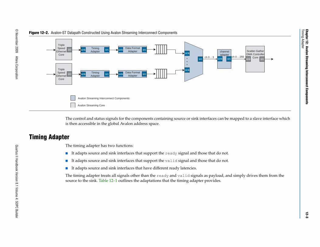
Figure 12–2 illustrates a datapath that connects a Triple Speed Ethernet MegaCore function to a Scatter-Gather DMA controller core using a timing adapter, data format adapter, and channel adapter so that the cores can interoperate.
Address Mapping
Figure 12–1. Example of an Avalon-ST Interconnect Component in an SOPC Builder System
Quartus II Handbook Version 8.1 Volume 4: SOPC Builder
The control and status signals for the components containing source or sink interfaces can be mapped to a slave interface which is then accessible in the global Avalon address space.
Timing AdapterThe timing adapter has two functions:
■ It adapts source and sink interfaces that support the ready signal and those that do not.
■ It adapts source and sink interfaces that support the valid signal and those that do not.
■ It adapts source and sink interfaces that have different ready latencies.
The timing adapter treats all signals other than the ready and valid signals as payload, and simply drives them from the source to the sink. Table 12–1 outlines the adaptations that the timing adapter provides.
Figure 12–2. Avalon-ST Datapath Constructed Using Avalon Streaming Interconnect Components
Resource Usage and PerformanceResource utilization for the timing adapter depends upon the function that it performs. Table 12–2 provides estimated resource utilization for seven different configurations of the timing adapter.
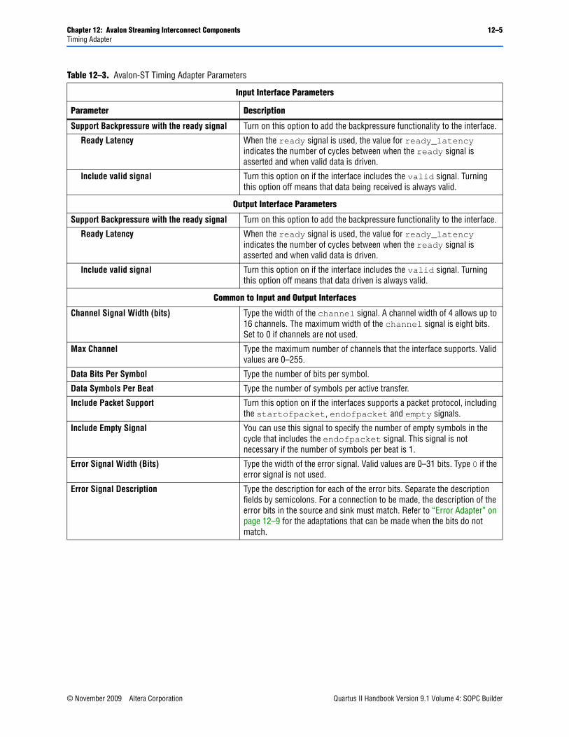
Instantiating the Timing Adapter in SOPC BuilderYou can use the Avalon-ST configuration wizard in SOPC Builder to specify the hardware features. Table 12–3 describes the options available on the Parameter Settings page of the configuration wizard
Table 12–1. Timing Adapter
Condition Adaptation
The source has ready, but the sink does not.
In this case, the source can respond to backpressure, but the sink never needs to apply it. The ready input to the source interface is connected directly to logical 1.
The source does not have ready, but the sink does.
The sink may apply backpressure, but the source is unable to respond to it. There is no logic that the adapter can insert that prevents data loss when the source asserts valid but the sink is not ready. The adapter provides simulation time error messages and an error indication if data is ever lost. The user is presented with a warning, and the connection is allowed.
The source and sink both support backpressure, but the sink’s ready latency is greater than the source's.
The source responds to ready assertion or deassertion faster than the sink requires it. A number of pipeline stages equal to the difference in ready latency are inserted in the ready path from the sink back to the source, causing the source and the sink to see the same cycles as ready cycles.
The source and sink both support backpressure, but the sink’s ready latency is less than the source's.
The source cannot respond to ready assertion or deassertion in time to satisfy the sink. A buffer whose depth is equal to the difference in ready latency is inserted to compensate for the source’s inability to respond in time.
Table 12–2. Timing Adapter Estimated Resource Usage and Performance
Input Ready
Latency
Output Ready
Latency
Stratix® II and Stratix II GX (Approximate LEs) Cyclone® II Stratix (Approximate LEs)
Support Backpressure with the ready signal Turn on this option to add the backpressure functionality to the interface.
Ready Latency When the ready signal is used, the value for ready_latency indicates the number of cycles between when the ready signal is asserted and when valid data is driven.
Include valid signal Turn this option on if the interface includes the valid signal. Turning this option off means that data being received is always valid.
Output Interface Parameters
Support Backpressure with the ready signal Turn on this option to add the backpressure functionality to the interface.
Ready Latency When the ready signal is used, the value for ready_latency indicates the number of cycles between when the ready signal is asserted and when valid data is driven.
Include valid signal Turn this option on if the interface includes the valid signal. Turning this option off means that data driven is always valid.
Common to Input and Output Interfaces
Channel Signal Width (bits) Type the width of the channel signal. A channel width of 4 allows up to 16 channels. The maximum width of the channel signal is eight bits. Set to 0 if channels are not used.
Max Channel Type the maximum number of channels that the interface supports. Valid values are 0–255.
Data Bits Per Symbol Type the number of bits per symbol.
Data Symbols Per Beat Type the number of symbols per active transfer.
Include Packet Support Turn this option on if the interfaces supports a packet protocol, including the startofpacket, endofpacket and empty signals.
Include Empty Signal You can use this signal to specify the number of empty symbols in the cycle that includes the endofpacket signal. This signal is not necessary if the number of symbols per beat is 1.
Error Signal Width (Bits) Type the width of the error signal. Valid values are 0–31 bits. Type 0 if the error signal is not used.
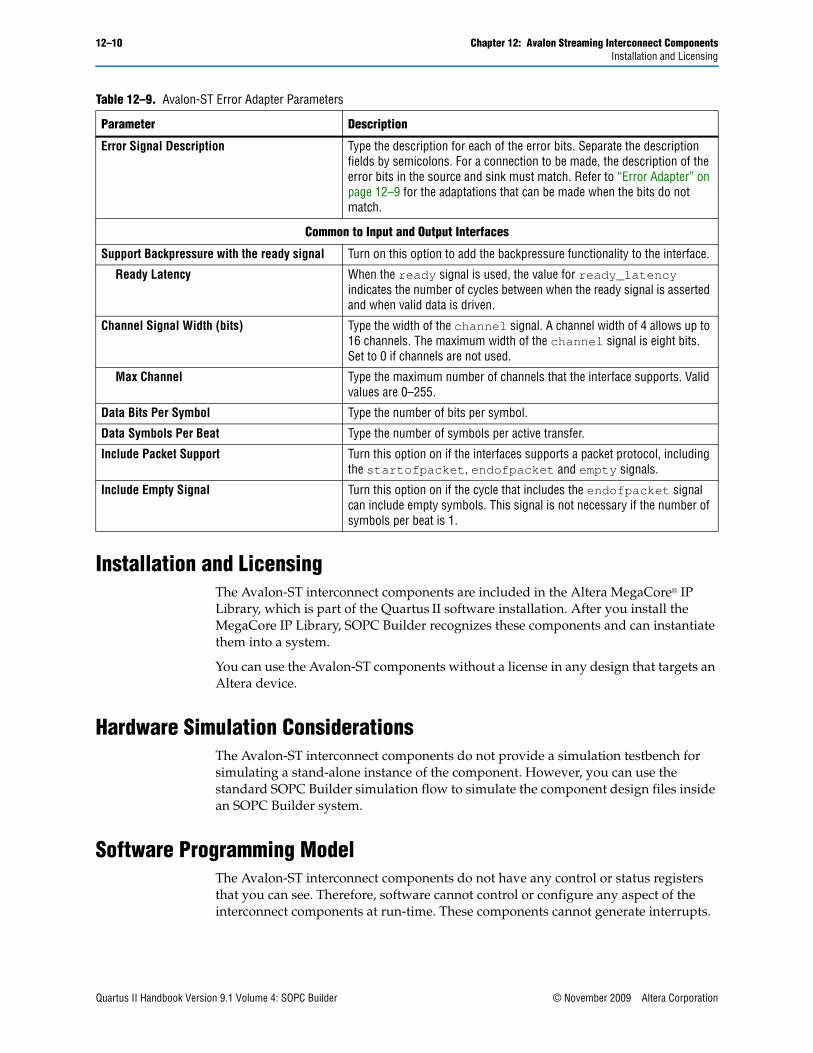
Error Signal Description Type the description for each of the error bits. Separate the description fields by semicolons. For a connection to be made, the description of the error bits in the source and sink must match. Refer to “Error Adapter” on page 12–9 for the adaptations that can be made when the bits do not match.
12–6 Chapter 12: Avalon Streaming Interconnect ComponentsData Format Adapter
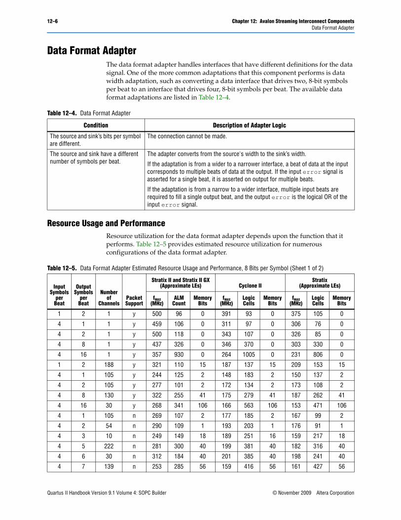
Data Format AdapterThe data format adapter handles interfaces that have different definitions for the data signal. One of the more common adaptations that this component performs is data width adaptation, such as converting a data interface that drives two, 8-bit symbols per beat to an interface that drives four, 8-bit symbols per beat. The available data format adaptations are listed in Table 12–4.
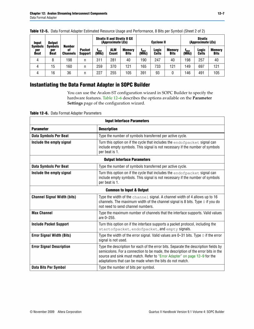
Resource Usage and PerformanceResource utilization for the data format adapter depends upon the function that it performs. Table 12–5 provides estimated resource utilization for numerous configurations of the data format adapter.
Table 12–4. Data Format Adapter
Condition Description of Adapter Logic
The source and sink’s bits per symbol are different.
The connection cannot be made.
The source and sink have a different number of symbols per beat.
The adapter converts from the source's width to the sink’s width.
If the adaptation is from a wider to a narrower interface, a beat of data at the input corresponds to multiple beats of data at the output. If the input error signal is asserted for a single beat, it is asserted on output for multiple beats.
If the adaptation is from a narrow to a wider interface, multiple input beats are required to fill a single output beat, and the output error is the logical OR of the input error signal.
Table 12–5. Data Format Adapter Estimated Resource Usage and Performance, 8 Bits per Symbol (Sheet 1 of 2)
Input Symbols
per Beat
Output Symbols
per Beat
Number of
ChannelsPacket Support
Stratix II and Stratix II GX (Approximate LEs) Cyclone II
Stratix(Approximate LEs)
fMAX(MHz)
ALM Count
Memory Bits
fMAX(MHz)
Logic Cells
Memory Bits
fMAX(MHz)
Logic Cells
Memory Bits
1 2 1 y 500 96 0 391 93 0 375 105 0
4 1 1 y 459 106 0 311 97 0 306 76 0
4 2 1 y 500 118 0 343 107 0 326 85 0
4 8 1 y 437 326 0 346 370 0 303 330 0
4 16 1 y 357 930 0 264 1005 0 231 806 0
1 2 188 y 321 110 15 187 137 15 209 153 15
4 1 105 y 244 125 2 148 183 2 150 137 2
4 2 105 y 277 101 2 172 134 2 173 108 2
4 8 130 y 322 255 41 175 279 41 187 262 41
4 16 30 y 268 341 106 166 563 106 153 471 106
4 1 105 n 269 107 2 177 185 2 167 99 2
4 2 54 n 290 109 1 193 203 1 176 91 1
4 3 10 n 249 149 18 189 251 16 159 217 18
4 5 222 n 281 300 40 199 381 40 182 316 40
4 6 30 n 312 184 40 201 385 40 198 241 40
4 7 139 n 253 285 56 159 416 56 161 427 56
Chapter 12: Avalon Streaming Interconnect Components 12–7Data Format Adapter
Instantiating the Data Format Adapter in SOPC BuilderYou can use the Avalon-ST configuration wizard in SOPC Builder to specify the hardware features. Table 12–6 describes the options available on the Parameter Settings page of the configuration wizard.
4 8 198 n 311 281 40 190 247 40 198 257 40
4 15 160 n 259 370 121 165 733 121 149 697 121
4 16 36 n 227 255 105 391 93 0 146 491 105
Table 12–5. Data Format Adapter Estimated Resource Usage and Performance, 8 Bits per Symbol (Sheet 2 of 2)
Input Symbols
per Beat
Output Symbols
per Beat
Number of
ChannelsPacket Support
Stratix II and Stratix II GX (Approximate LEs) Cyclone II
Stratix(Approximate LEs)
fMAX(MHz)
ALM Count
Memory Bits
fMAX(MHz)
Logic Cells
Memory Bits
fMAX(MHz)
Logic Cells
Memory Bits
Table 12–6. Data Format Adapter Parameters
Input Interface Parameters
Parameter Description
Data Symbols Per Beat Type the number of symbols transferred per active cycle.
Include the empty signal Turn this option on if the cycle that includes the endofpacket signal can include empty symbols. This signal is not necessary if the number of symbols per beat is 1.
Output Interface Parameters
Data Symbols Per Beat Type the number of symbols transferred per active cycle.
Include the empty signal Turn this option on if the cycle that includes the endofpacket signal can include empty symbols. This signal is not necessary if the number of symbols per beat is 1.
Common to Input & Output
Channel Signal Width (bits) Type the width of the channel signal. A channel width of 4 allows up to 16 channels. The maximum width of the channel signal is 8 bits. Type 0 if you do not need to send channel numbers.
Max Channel Type the maximum number of channels that the interface supports. Valid values are 0–255.
Include Packet Support Turn this option on if the interface supports a packet protocol, including the startofpacket, endofpacket, and empty signals.
Error Signal Width (Bits) Type the width of the error signal. Valid values are 0–31 bits. Type 0 if the error signal is not used.
Error Signal Description Type the description for each of the error bits. Separate the description fields by semicolons. For a connection to be made, the description of the error bits in the source and sink must match. Refer to “Error Adapter” on page 12–9 for the adaptations that can be made when the bits do not match.
Data Bits Per Symbol Type the number of bits per symbol.
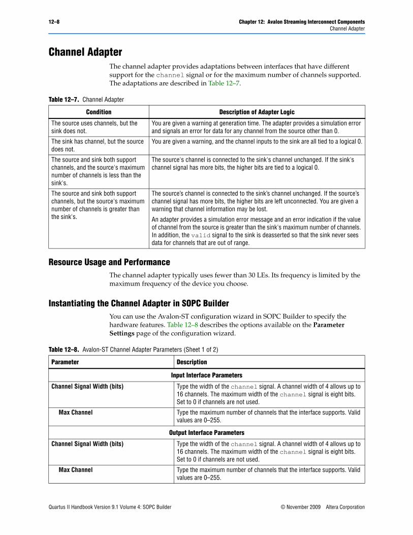
Channel AdapterThe channel adapter provides adaptations between interfaces that have different support for the channel signal or for the maximum number of channels supported. The adaptations are described in Table 12–7.
Resource Usage and PerformanceThe channel adapter typically uses fewer than 30 LEs. Its frequency is limited by the maximum frequency of the device you choose.
Instantiating the Channel Adapter in SOPC BuilderYou can use the Avalon-ST configuration wizard in SOPC Builder to specify the hardware features. Table 12–8 describes the options available on the Parameter Settings page of the configuration wizard.
.
Table 12–7. Channel Adapter
Condition Description of Adapter Logic
The source uses channels, but the sink does not.
You are given a warning at generation time. The adapter provides a simulation error and signals an error for data for any channel from the source other than 0.
The sink has channel, but the source does not.
You are given a warning, and the channel inputs to the sink are all tied to a logical 0.
The source and sink both support channels, and the source's maximum number of channels is less than the sink's.
The source's channel is connected to the sink's channel unchanged. If the sink's channel signal has more bits, the higher bits are tied to a logical 0.
The source and sink both support channels, but the source's maximum number of channels is greater than the sink's.
The source’s channel is connected to the sink’s channel unchanged. If the source’s channel signal has more bits, the higher bits are left unconnected. You are given a warning that channel information may be lost.
An adapter provides a simulation error message and an error indication if the value of channel from the source is greater than the sink's maximum number of channels. In addition, the valid signal to the sink is deasserted so that the sink never sees data for channels that are out of range.
Table 12–8. Avalon-ST Channel Adapter Parameters (Sheet 1 of 2)
Parameter Description
Input Interface Parameters
Channel Signal Width (bits) Type the width of the channel signal. A channel width of 4 allows up to 16 channels. The maximum width of the channel signal is eight bits. Set to 0 if channels are not used.
Max Channel Type the maximum number of channels that the interface supports. Valid values are 0–255.
Output Interface Parameters
Channel Signal Width (bits) Type the width of the channel signal. A channel width of 4 allows up to 16 channels. The maximum width of the channel signal is eight bits. Set to 0 if channels are not used.
Max Channel Type the maximum number of channels that the interface supports. Valid values are 0–255.
Error AdapterThe error adapter ensures that per-bit error information provided by source interfaces is correctly connected to the sink interface's input error signal. The adaptations are described in Table 12–9:
Instantiating the Error Adapter in SOPC BuilderYou can use the Avalon-ST configuration wizard in SOPC Builder to specify the hardware features. Table 12–9 describes the options available on the Parameter Settings page of the configuration wizard.
.
Common to Input and Output Interfaces
Support Backpressure with the ready signal Turn on this option to add the backpressure functionality to the interface.
Ready Latency When the ready signal is used, the value for ready_latency indicates the number of cycles between when the ready signal is asserted and when valid data is driven.
Data Bits Per Symbol Type the number of bits per symbol.
Data Symbols Per Beat Type the number of symbols per active transfer.
Include Packet Support Turn this option on if the interfaces supports a packet protocol, including the startofpacket, endofpacket and empty signals.
Include Empty Signal You can use this signal to specify the number of empty symbols in the cycle that includes the endofpacket signal. This signal is not necessary if the number of symbols per beat is 1.
Error Signal Width (bits) Type the width of the error signal. Valid values are 0–31 bits. Type 0 if you do not need to send error values.
Error Signal Description Type the description for each of the error bits. Separate the description fields by semicolons. For a connection to be made, the description of the error bits in the source and sink must match. Refer to “Error Adapter” on page 12–9 for the adaptations that can be made when the bits do not match.
Table 12–8. Avalon-ST Channel Adapter Parameters (Sheet 2 of 2)
Parameter Description
Table 12–9. Avalon-ST Error Adapter Parameters
Parameter Description
Input Interface Parameters
Error Signal Width (bits) Type the width of the error signal. Valid values are 0–31 bits. Type 0 if the error signal is not used.
Error Signal Description Type the description for each of the error bits. Separate the description fields by semicolons. For a connection to be made, the description of the error bits in the source and sink must match. Refer to “Error Adapter” on page 12–9 for the adaptations that can be made when the bits do not match.
Output Interface Parameters
Error Signal Width (bits) Type the width of the error signal. Valid values are 0–31 bits. Type 0 if you do not need to send error values.
12–10 Chapter 12: Avalon Streaming Interconnect ComponentsInstallation and Licensing
Installation and LicensingThe Avalon-ST interconnect components are included in the Altera MegaCore® IP Library, which is part of the Quartus II software installation. After you install the MegaCore IP Library, SOPC Builder recognizes these components and can instantiate them into a system.
You can use the Avalon-ST components without a license in any design that targets an Altera device.
Hardware Simulation ConsiderationsThe Avalon-ST interconnect components do not provide a simulation testbench for simulating a stand-alone instance of the component. However, you can use the standard SOPC Builder simulation flow to simulate the component design files inside an SOPC Builder system.
Software Programming ModelThe Avalon-ST interconnect components do not have any control or status registers that you can see. Therefore, software cannot control or configure any aspect of the interconnect components at run-time. These components cannot generate interrupts.
Error Signal Description Type the description for each of the error bits. Separate the description fields by semicolons. For a connection to be made, the description of the error bits in the source and sink must match. Refer to “Error Adapter” on page 12–9 for the adaptations that can be made when the bits do not match.
Common to Input and Output Interfaces
Support Backpressure with the ready signal Turn on this option to add the backpressure functionality to the interface.
Ready Latency When the ready signal is used, the value for ready_latency indicates the number of cycles between when the ready signal is asserted and when valid data is driven.
Channel Signal Width (bits) Type the width of the channel signal. A channel width of 4 allows up to 16 channels. The maximum width of the channel signal is eight bits. Set to 0 if channels are not used.
Max Channel Type the maximum number of channels that the interface supports. Valid values are 0–255.
Data Bits Per Symbol Type the number of bits per symbol.
Data Symbols Per Beat Type the number of symbols per active transfer.
Include Packet Support Turn this option on if the interfaces supports a packet protocol, including the startofpacket, endofpacket and empty signals.
Include Empty Signal Turn this option on if the cycle that includes the endofpacket signal can include empty symbols. This signal is not necessary if the number of symbols per beat is 1.
Table 12–9. Avalon-ST Error Adapter Parameters
Parameter Description
Chapter 12: Avalon Streaming Interconnect Components 12–11Document Revision History