Altera Corporation Section IV–1 Preliminary Section IV. HardCopy Design Center Migration Process This section provides information on the software support for HardCopy ® Stratix ® devices. This section contains the following: ■ Chapter 13, Back-End Design Flow for HardCopy Series Devices ■ Chapter 14, Back-End Timing Closure for HardCopy Series Devices Revision History Refer to each chapter for its own specific revision history. For information on when each chapter was updated, refer to the Chapter Revision Dates section, which appears in the complete handbook.
Transcript
Altera Corporation Section IV–1Preliminary
Section IV. HardCopy DesignCenter Migration Process
This section provides information on the software support for HardCopy® Stratix® devices.
This section contains the following:
■ Chapter 13, Back-End Design Flow for HardCopy Series Devices
■ Chapter 14, Back-End Timing Closure for HardCopy Series Devices
Revision History Refer to each chapter for its own specific revision history. For information on when each chapter was updated, refer to the Chapter Revision Dates section, which appears in the complete handbook.
Section IV–2 Altera CorporationPreliminary
Revision History HardCopy Series Handbook, Volume 1
Altera Corporation 13–1September 2008
13. Back-End Design Flow forHardCopy Series Devices
Introduction This chapter discusses the back-end design flow executed by the HardCopy® Design Center when developing your HardCopy series device. The chapter is divided into two sections:
■ HardCopy II Back-End Design Flow■ HardCopy Stratix® and HardCopy APEX™ Back-End Design Flow
1 For more information on the HardCopy II, HardCopy Stratix, and HardCopy APEX families, refer to the respective sections for these families in the HardCopy Series Handbook.
HardCopy II Back-End Design Flow
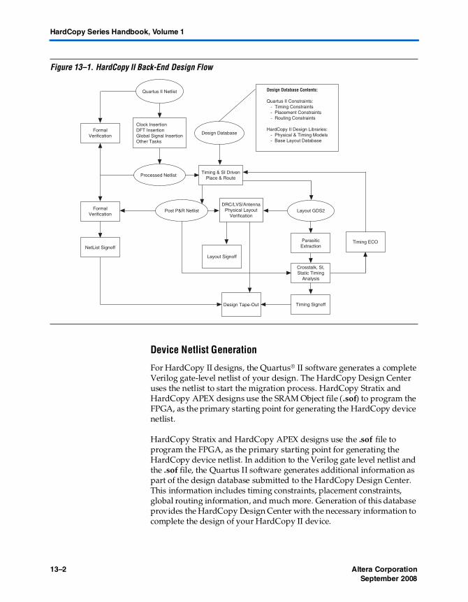
This section outlines the back-end design process for HardCopy II devices, which occurs in several steps. Figure 13–1 illustrates these steps. The design process uses both proprietary and third-party EDA tools. The HardCopy II device design flow is different from that of previous HardCopy families (HardCopy Stratix and HardCopy APEX devices). The following sections outline these differences.
H51019-1.4
13–2 Altera Corporation September 2008
HardCopy Series Handbook, Volume 1
Figure 13–1. HardCopy II Back-End Design Flow
Device Netlist Generation
For HardCopy II designs, the Quartus® II software generates a complete Verilog gate-level netlist of your design. The HardCopy Design Center uses the netlist to start the migration process. HardCopy Stratix and HardCopy APEX designs use the SRAM Object file (.sof) to program the FPGA, as the primary starting point for generating the HardCopy device netlist.
HardCopy Stratix and HardCopy APEX designs use the .sof file to program the FPGA, as the primary starting point for generating the HardCopy device netlist. In addition to the Verilog gate level netlist and the .sof file, the Quartus II software generates additional information as part of the design database submitted to the HardCopy Design Center. This information includes timing constraints, placement constraints, global routing information, and much more. Generation of this database provides the HardCopy Design Center with the necessary information to complete the design of your HardCopy II device.
HardCopy II Design Libraries: - Physical & Timing Models - Base Layout Database
Layout GDS2
Timing & SI Driven Place & Route
Parasitic Extraction
Crosstalk, SI, Static Timing
Analysis
Timing Signoff
Post P&R NetlistDRC/LVS/Antenna
Physical Layout Verification
Processed Netlist
NetList Signoff
Formal Verification
Quartus II Netlist
Clock Insertion DFT Insertion Global Signal Insertion Other Tasks
Design Database
Timing ECO
Altera Corporation 13–3September 2008
HardCopy II Back-End Design Flow
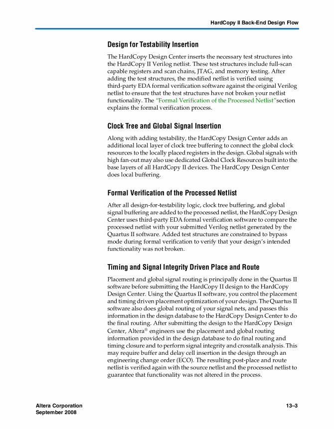
Design for Testability Insertion
The HardCopy Design Center inserts the necessary test structures into the HardCopy II Verilog netlist. These test structures include full-scan capable registers and scan chains, JTAG, and memory testing. After adding the test structures, the modified netlist is verified using third-party EDA formal verification software against the original Verilog netlist to ensure that the test structures have not broken your netlist functionality. The “Formal Verification of the Processed Netlist”section explains the formal verification process.
Clock Tree and Global Signal Insertion
Along with adding testability, the HardCopy Design Center adds an additional local layer of clock tree buffering to connect the global clock resources to the locally placed registers in the design. Global signals with high fan-out may also use dedicated Global Clock Resources built into the base layers of all HardCopy II devices. The HardCopy Design Center does local buffering.
Formal Verification of the Processed Netlist
After all design-for-testability logic, clock tree buffering, and global signal buffering are added to the processed netlist, the HardCopy Design Center uses third-party EDA formal verification software to compare the processed netlist with your submitted Verilog netlist generated by the Quartus II software. Added test structures are constrained to bypass mode during formal verification to verify that your design’s intended functionality was not broken.
Timing and Signal Integrity Driven Place and Route
Placement and global signal routing is principally done in the Quartus II software before submitting the HardCopy II design to the HardCopy Design Center. Using the Quartus II software, you control the placement and timing driven placement optimization of your design. The Quartus II software also does global routing of your signal nets, and passes this information in the design database to the HardCopy Design Center to do the final routing. After submitting the design to the HardCopy Design Center, Altera® engineers use the placement and global routing information provided in the design database to do final routing and timing closure and to perform signal integrity and crosstalk analysis. This may require buffer and delay cell insertion in the design through an engineering change order (ECO). The resulting post-place and route netlist is verified again with the source netlist and the processed netlist to guarantee that functionality was not altered in the process.
13–4 Altera Corporation September 2008
HardCopy Series Handbook, Volume 1
Parasitic Extraction and Timing Analysis
After doing placement and routing on the design by the HardCopy Design Center, it generates the gds2 design file and extracts the parasitic resistance and capacitance values for timing analysis. Parasitic extraction uses the physical layout of the design stored in a .gds2 file to extract these resistance and capacitance values for all signal nets in the design. The HardCopy Design Center uses these parasitic values to calculate the path delays through the design for static timing analysis and crosstalk analysis.
Layout Verification
When the Timing Analysis reports that all timing requirements are met, the design layout goes into the final stage of verification for manufacturability. The HardCopy Design Center performs physical Design Rule Checking (DRC), antenna checking of long traces of signals in the layout, and a comparison of layout to the design netlist, commonly referred to as Layout Versus Schematic (LVS). These tasks guarantee that the layout contains the exact logic represented in the place-and-route netlist, and the physical layout conforms to 90-nm manufacturing rules.
Design Signoff
The Altera HardCopy II back-end design methodology has a thorough verification and signoff process, guaranteeing your design’s functionality. Signoff occurs after confirming the final place-and-route netlist functional verification, confirming layout verification for manufacturability, and the timing analysis reports meeting all requirements. After achieving all three signoff points, Altera begins the manufacturing of the HardCopy II devices.
Altera Corporation 13–5September 2008
HardCopy Stratix and HardCopy APEX Migration Flow
HardCopy Stratix and HardCopy APEX Migration Flow
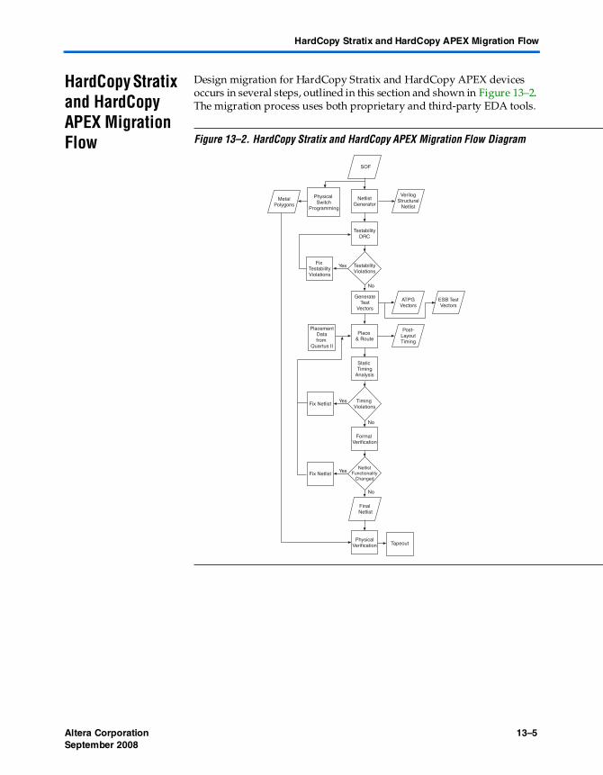
Design migration for HardCopy Stratix and HardCopy APEX devices occurs in several steps, outlined in this section and shown in Figure 13–2. The migration process uses both proprietary and third-party EDA tools.
Figure 13–2. HardCopy Stratix and HardCopy APEX Migration Flow Diagram
SOF
GenerateTest
Vectors
Place & Route
Fix Netlist Yes
Fix TestabilityViolations
Yes
No
No
No
Yes
Final Netlist
MetalPolygons
Physical Switch
Programming
NetlistGenerator
VerilogStructural
Netlist
TestabilityDRC
TestabilityViolations
ATPGVectors
ESB TestVectors
Post-LayoutTiming
Static Timing
Analysis
PhysicalVerification
NetlistFunctionality
Changed
Formal Verification
Fix Netlist
Timing Violations
Tapeout
Placement Data from
Quartus II
13–6 Altera Corporation September 2008
HardCopy Series Handbook, Volume 1
Netlist Generation
For HardCopy Stratix and HardCopy APEX designs, Altera migrates the Quartus II software-generated .sof file to a Verilog HDL structural netlist that describes how the following structural elements are configured in the design and how each structural element is connected to other structural elements:
■ Logic element (LE)■ Phase-locked loop (PLL)■ Digital signal processing (DSP) block■ Memory block■ Input/output element (IOE)
The information that describes the structural element configuration is converted into a physical coordinate format so that metal elements can be implemented on top of the pre-defined HardCopy series device-base array. Using the .sof file for netlist extraction helps ensure that the HardCopy series device contains the same functional implementation that was used in the FPGA version of the design.
Testability Audit
The Design Center performs an audit for testability violations when the Verilog HDL netlist is available. This audit ensures that all built-in scan chain structures will work reliably while testing the HardCopy series devices. Certain circuit structures, such as gated clocks, gated resets, oscillators, pulse generators, or other types of asynchronous circuit structures makes the performance of scan chain structures unreliable. During the testability audit, all such circuit structures are detected and disabled when the device is put into test mode.
Placement
Beginning with version 4.2, the Quartus II software supports all HardCopy series devices. The HardCopy Timing Optimization Wizard in the Quartus II software is used for HardCopy Stratix devices and generates placement information of the design when it is mapped to the HardCopy Stratix base array. This placement information is read in and directly used by the place-and-route tool during migration to the equivalent HardCopy Stratix device.
f For more information on how to use the HardCopy Timing Optimization Wizard, refer to the Quartus II Support for HardCopy Stratix Devices chapter. For more information on Quartus II features for HardCopy II devices, refer to the Quartus II Support for HardCopy II Devices chapter.
Altera Corporation 13–7September 2008
HardCopy Stratix and HardCopy APEX Migration Flow
To generate placement data, the Quartus II software uses the .sof file to generate the netlist, as described in “Netlist Generation” on page 13–6. The netlist is then read into a place-and-route tool. The placement optimization is based on the netlist connectivity and the design’s timing constraints. The placement of all IOEs is fixed. After placement is complete, the Quartus II software generates the scan chain ordering information so the scan paths can be connected.
Test Vector Generation
Memory test vectors and memory built-in self-test (BIST) circuitry ensure that all memory bits function correctly. Automatic test pattern generation (ATPG) vectors test all LE, DSP, and IOE logic. These vectors ensure that a high stuck-at-fault coverage is achieved. The target fault coverage for all HardCopy Stratix devices is near 100%.
When the testability audit is successfully completed and the scan chains have been re-ordered, the Design Center can generate memory and ATPG test vectors. When test vector generations are complete, they are simulated to verify their correctness.
Routing
Routing involves generating the physical interconnect between every element in the design. At this stage, physical design rule violations are fixed. For example, nodes with large fan-outs need to be buffered. Otherwise, these signal transition times are too slow, and the device’s power consumption increases. All other types of physical design rule violations are also fixed during this stage, such as antenna violations, crosstalk violations, and metal spacing violations.
Extracted Delay Calculation
Interconnect parasitic capacitance and resistance information is generated after the routing is complete. This information is then converted into a Standard Delay File (.sdf) with a delay calculation tool, and timing is generated for minimum and maximum delays.
Static Timing Analysis and Timing Closure
The design timing is checked and corrected after place and route using the post-layout generated .sdf file. Setup time violations are corrected in two ways. First, extra buffers can be inserted to speed up slow signals. Second, if buffer insertion does not completely fix the setup violation, the placement can be re-optimized.
13–8 Altera Corporation September 2008
HardCopy Series Handbook, Volume 1
Setup time violations are rare in HardCopy II and HardCopy Stratix devices because the die sizes are considerably smaller than the equivalent Stratix II and Stratix devices. Statistically, the interconnect loading and distance is much smaller in HardCopy Stratix devices, so the device operates at a higher clock frequency. Hold-time violations are fixed by inserting delay elements into fast data paths.
As part of the timing analysis process, crosstalk analysis is also performed to remove any crosstalk effects that could be encountered in the device after it has been manufactured. This ensures signal integrity in the device resulting in proper functionality and satisfactory performance.
After implementing all timing violation corrections in the netlist, the place and route is updated to reflect the changes. This process is repeated until all timing violations are removed. Typically, only a single iteration is required after the initial place and route. Finally, static functional verification is tested after this stage to double-check the netlist integrity.
Formal Verification
After any change to the netlist, you must verify its integrity through static functional verification (or formal verification) techniques. These techniques show whether two versions of a design are functionally identical when certain constraints are applied. For example, after test fixes, the netlist must be logically equivalent to the netlist state before test fixes, when the test mode is disabled. This technique does not rely on any customer-supplied functional simulation vectors. Altera uses third-party formal verification software to confirm that the back-end implementation matches the netlist generated from the FPGA’s .sof programming file.
Physical Verification
Before manufacturing the metal customization layers, the physical programming information must be verified. This stage involves cross-checking for physical design rule violations in the layout database, and also checking that the circuit was physically implemented correctly. These processes are commonly known as running design rule check and layout-versus-schematic verification.
Manufacturing Metallization masks are created to manufacture HardCopy series devices. After manufacturing, the parts are tested using the test vectors that were developed as part of the implementation process.
Altera Corporation 13–9September 2008
Testing
Testing HardCopy series devices are fully tested as part of the manufacturing process. Testing does not require user-specific simulation vectors, because every HardCopy series device utilizes full scan path technology. This means that every node inside the device is both controllable and observable through one or more of the package pins of the device. The scan paths, or “scan chains,” are exercised through ATPG. This ensures a high-confidence level in the detection of all manufacturing defects.
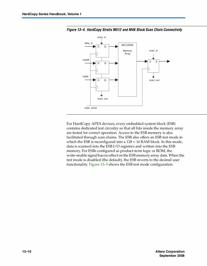
Every register in the HardCopy series device belongs to a scan chain. Scan chains are test features that exist in ASICs to ensure that there is access to all internal nodes of a design. With scan chains, defective parts can be screened out during the manufacturing process. Scan chain registers are constructed by combining the original FPGA register with a 2-to-1 multiplexer. In normal user mode, the multiplexer is transparent to the user. In scan mode, the registers in the device are connected into a long-shift register so that automatic test pattern generation vectors can be scanned into and out of the device. Several independent scan chains exist in the HardCopy series device to keep scan chain lengths short, and are run in parallel to keep tester time per device short. Figure 13–3 shows a diagram of a scan register.
In addition to the scan circuitry (Figure 13–3), which is designed to test all LEs and IOEs, both M512 and M4K blocks (Figure 13–4) have the same scan chain structure so that all bits inside the memory array are tested for correct operation. The M512 and M4K RAM bits are tested by scanning data into the M512 and M4K blocks’ data_in, write address (waddr), and read address (raddr) registers. After each vector has been scanned into the HardCopy Stratix device, a write enable (WE) pulse is generated to write the data into the M512 and M4K blocks. A read enable (RE) pulse is also generated to read data out of the M512 and M4K blocks. The data read back from the M512 and M4K blocks are scanned out of the device via the data_out registers. Figure 13–4 shows the M512 and M4K blocks’ scan chain connectivity.
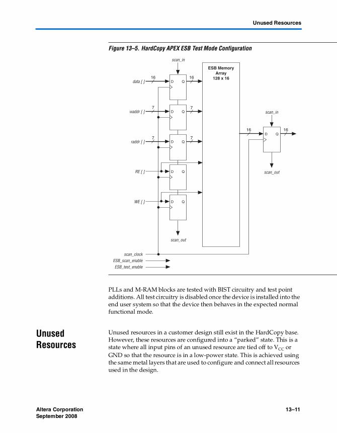
For HardCopy APEX devices, every embedded system block (ESB) contains dedicated test circuitry so that all bits inside the memory array are tested for correct operation. Access to the ESB memory is also facilitated through scan chains. The ESB also offers an ESB test mode in which the ESB is reconfigured into a 128 × 16 RAM block. In this mode, data is scanned into the ESB I/O registers and written into the ESB memory. For ESBs configured as product-term logic or ROM, the write-enable signal has no effect on the ESB memory array data. When the test mode is disabled (the default), the ESB reverts to the desired user functionality. Figure 13–5 shows the ESB test mode configuration.
D Q
M512/M4K
Memory Array
D Q
D Q D Q
scan_in
scan_out
data_in
waddr
raddr
scan_in
scan_out
scan_clock
Altera Corporation 13–11September 2008
Unused Resources
Figure 13–5. HardCopy APEX ESB Test Mode Configuration
PLLs and M-RAM blocks are tested with BIST circuitry and test point additions. All test circuitry is disabled once the device is installed into the end user system so that the device then behaves in the expected normal functional mode.
Unused Resources
Unused resources in a customer design still exist in the HardCopy base. However, these resources are configured into a “parked” state. This is a state where all input pins of an unused resource are tied off to VCC or GND so that the resource is in a low-power state. This is achieved using the same metal layers that are used to configure and connect all resources used in the design.
D Q
scan_in
scan_in
data [ ]
D Qwaddr [ ]
D Qraddr [ ]
D QRE [ ]
D QWE [ ]
scan_out
D Q
scan_out
16 16
77
7 7
16
scan_clockESB_scan_enableESB_test_enable
16
ESB Memory Array
128 x 16
13–12 Altera Corporation September 2008
HardCopy Series Handbook, Volume 1
Conclusion The HardCopy series back-end design methodology ensures that your design seamlessly migrates from your prototype FPGA to a HardCopy device. This methodology, matched with Altera’s unique FPGA prototyping and migration process, provides an excellent way for you to develop your design for production.
1 For more information about how to start building your HardCopy series design, contact your Altera Field Applications Engineer.
f For more information on HardCopy products and solutions, refer to the HardCopy Series Handbook.
Document Revision History
Table 13–1 shows the revision history for this chapter.
Table 13–1. Document Revision History
Date and Document Version Changes Made Summary of Changes
September 2008, v1.4
Updated chapter number and revision history. —
June 2007, v1.3 Minor text edits. —
December 2006 v1.2
Added revision history. —
March 2006 Formerly chapter 13; no content change. —
October 2005 v1.1 ● Graphic updates● Minor edits
—
January 2005v1.0
Initial release of Chapter 13, Back-End Design Flow for HardCopy Series Devices.
—
Altera Corporation 14–1September 2008 Preliminary
14. Back-End Timing Closurefor HardCopy Series Devices
Introduction Back-end implementation of HardCopy® series devices meet design requirements through a timing closure process similar to the methodology used for today’s standard cell ASICs.
The Quartus® II software provides a pre-layout estimation of your HardCopy design performance and then the Altera® HardCopy Design Center uses industry leading EDA software to complete the back-end layout and extract the final timing results prior to tape-out.
f For more information on the HardCopy back-end design flow, refer to the HardCopy Series Back-End Design Flow chapter in the HardCopy Series Device Handbook.
This chapter describes how Altera ensures that HardCopy series devices meet their required timing performance.
Timing Analysis of HardCopy Prototype Device
You should perform timing analysis on the FPGA prototype implementation of the design before migrating to HardCopy. For HardCopy II designs, timing analysis should also be performed after successfully fitting the design in a HardCopy II device with Quartus II software. Timing analysis determines whether the design’s performance meets the required timing goals.
The timing analysis must be done for both setup and hold time checks on all design paths, including internal paths and input and output paths. Measuring these parameters against performance goals ensures that the FPGA design functions as planned in the end-target system.
f For more information on timing analysis of Altera devices, refer to the Timing Analysis section in volume 3 of the Quartus II Handbook.
After the FPGA design is stabilized, fully tested in-system and satisfies the HardCopy series design rules, the design can be migrated to a HardCopy series device. Altera performs rigorous timing analysis on the HardCopy series device during its implementation, ensuring that it meets the required timing goals. Because the critical timing paths of the HardCopy version of a design may be different from the corresponding paths in the FPGA version, meeting the required timing goals constrained in the Quartus II software is particularly important. Additional
H51013-2.4
14–2 Altera CorporationSeptember 2008
HardCopy Series Handbook, Volume 1
performance gains are design dependent, and the percentage of performance improvement can be different for each clock domain of your design.
Timing differences between the FPGA design and the equivalent HardCopy series device can exist for several reasons. While maintaining the same set of features as the corresponding FPGA, HardCopy series devices have a highly optimized die size to make them as small as possible. Because of the customized interconnect structure that makes this optimization possible, the delay through each signal path is different from the original FPGA design.
Cell Structure Meeting system timing goals in an ASIC design can be very challenging and can easily consume many months of engineering effort. The slower development process exists because, in today’s silicon technology (0.18 μm, 0.13 μm, and 90 nm), the delay associated with interconnect dominates the delay associated with the transistors used to make the logic gates. Consequently, ASIC performance is sensitive to the physical placement and routing of the logic blocks that make up the design.
HardCopy II
HardCopy II devices use timing constraints to drive placement and routing of logic into the fabric of HCells. Each Stratix II Adaptive Look-up Table (ALUT) is implemented in HCell Macros in the HardCopy II device. HCell Macros are pre-defined and characterized libraries built out of HCells. The Quartus II software performs the placement and global routing of all HCell Macros and this information is forward-annotated to the HardCopy Design Center for final back-end implementation and timing closure.
HardCopy Stratix, HardCopy APEX
HardCopy Stratix® and HardCopy APEX™ are structurally identical to their respective FPGA counterparts. There is no re-synthesis or library re-mapping required. Since the interconnect lengths are much smaller in the HardCopy series device than they are in the FPGA, the place-and-route engine compiling the HardCopy series design has a considerably less difficult task than it does in an equivalent ASIC development. Coupled with detailed timing constraints, the place-and-route is timing driven.
Altera Corporation 14–3September 2008
Clock Tree Structure
Clock Tree Structure
The following section describes the clock tree structure for the HardCopy device family.
HardCopy II
HardCopy II devices offer a fine-grained architecture of HCells which are used to build HCell Macros for standard logic functions. The pre-built metal layers of HardCopy II devices contain the same global clock tree resources as those available in Stratix II devices, though they are smaller in HardCopy II devices because of the difference in die size. The top levels of the dedicated global clock networks in HardCopy II are pre-routed in the non-custom metal layers. The lowest level of clock tree buffering and routing is done using custom metal routing. Local buffering can be done using HCell Macros to fix any clock skew issues. HCell Macros are used to create registers, and local custom routing is needed to connect the clock networks to these HCell Macro registers. These tasks are performed as part of the HardCopy Design Center process.
HardCopy Stratix
HardCopy Stratix devices have the same global clock tree resources as Stratix FPGA devices. The construction of non-customizable layers of silicon minimizes global clock tree skew. HardCopy Stratix devices with clock trees using global clock resources have smaller clock insertion delay than Stratix FPGA devices because the HardCopy Stratix devices have a smaller die area. The use of clock tree synthesis to build small localized clock trees using the existing buffer resources in HardCopy Stratix devices automatically implements clock trees using fast regional clock resources in Stratix FPGA devices.
HardCopy APEX
The HardCopy APEX device architecture is based on the APEX 20KE and APEX 20KC devices. The same dedicated clock trees (CLK[3..0]) that exist in APEX 20KE and APEX 20KC devices also exist in the corresponding HardCopy APEX device. These clock trees are carefully designed and optimized to minimize the clock skew over the entire device. The clock tree is balanced by maintaining the same loading at the end of each point of the clock tree, regardless of what resources (logic elements [LEs], embedded system blocks [ESBs], and input/output elements [IOEs]) are used in any design. The insertion delay of the HardCopy APEX dedicated clock trees is marginally faster than in the corresponding APEX 20KE or APEX 20KC FPGA device because of the smaller footprint of the HardCopy device silicon. This difference is less than 1 ns.
14–4 Altera CorporationSeptember 2008
HardCopy Series Handbook, Volume 1
Because there is a large area overhead for the global signals that may not be used on every design, the FAST bidirectional pins (FAST[3..0]) do not have dedicated pre-built clock or buffer trees in HardCopy APEX devices. If any of the FAST signals are used as clocks, the place-and-route tool synthesizes a clock tree after the placement of the design has occurred. The skew and insertion delay of these synthesized clock trees is carefully controlled, ensuring that the timing requirements of the design are met. You can also use the FAST signals as high fan-out reset or enable signals. For these cases, skew is usually less important than insertion delay. To reiterate, a buffer tree is synthesized after the design placement.
The clock or buffer trees that are synthesized for the FAST pins are built out of special cells in the HardCopy APEX base design. These cells do not exist in the FPGA, and they are used in the HardCopy APEX design exclusively to meet timing and testing goals. They are not available to make any logical changes to the design as implemented in the FPGA. These resources are called the strip of auxiliary gates (SOAG). There is one strip per MegaLAB™ structure in HardCopy APEX devices. Each SOAG consists of a number of primitive cells, and there are approximately 10 SOAG primitive cells per logic array block (LAB). Several SOAG primitives can be combined to form more complex logic, but the majority of SOAG resources are used for buffer tree, clock tree, and delay cell generation.
f For detailed information on the HardCopy APEX series device architecture, including SOAG resources, refer to the HardCopy APEX Device Family Data Sheet section in volume 1 of the HardCopy Series Handbook.
Importance of Timing Constraints
After capturing the information, Altera directly checks all timing of the HardCopy series device before tape-out occurs. It is important to constrain the FPGA and HardCopy devices for the exact timing requirements that need to be achieved. Timing violations seen in the Quartus II project or in the HardCopy Design Center migration process must be fixed or waived prior to the design being manufactured.
Correcting Timing Violations
After generating the customized metal interconnect for the HardCopy series device, Altera checks the design timing with a static timing analysis tool. The static timing analysis tool reports timing violations and then the HardCopy Design Center corrects the violations.
Altera Corporation 14–5September 2008
Importance of Timing Constraints
Hold-Time Violations
Because the interconnect in a HardCopy series device is customized for a particular application, it is possible that hold-time (tH) violations exist in the HardCopy series device after place-and-route occurs. A hold violation exists if the sum of the delay in the clock path between two registers plus the micro hold time of the destination register is greater than the delay of the data path from the source register to the destination register. The following equation describes this relationship.
tH slack = data delay - clock delay - µtH
If a negative slack value exists, a hold-time violation exists. Any hold-time violation present in the HardCopy series design database after the interconnect data is generated is removed by inserting the appropriate delay in the data path. The inserted delay is large enough to guarantee no hold violation under fast, low-temperature, high-voltage conditions.
An Example HardCopy APEX Hold-Time Violation Fix
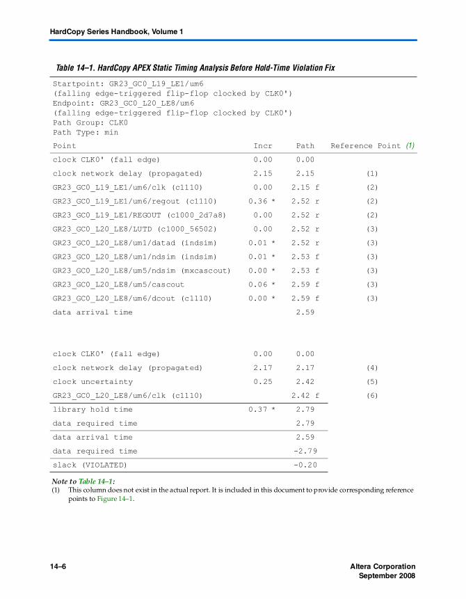
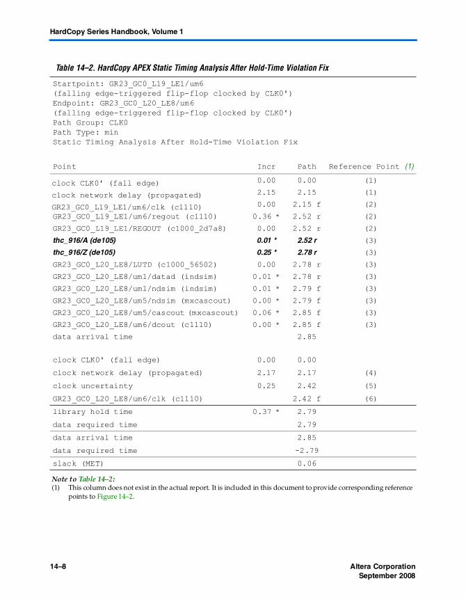
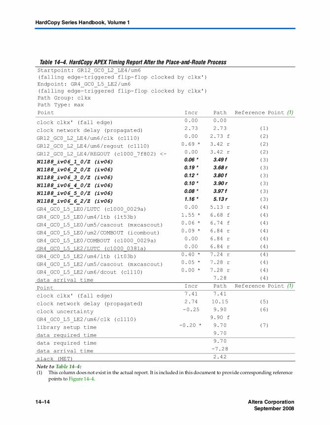
Table 14–1 shows an example report of a Synopsys PrimeTime static timing analysis of a HardCopy APEX design. The first report shows that the circuit has a hold-time violation and a negative slack value. The second result shows the timing report for the same path after fixing the hold violation. Part of the HardCopy implementation process is to generate the instance and cell names shown in these reports. The physical location of those elements in the device determines the generation of the names.
In this timing report, the slack of this path is reported as 0.06 ns. Therefore, this path does not have a hold-time violation. This path was fixed by the insertion of a delay cell (del05) into the data path, which starts at the REGOUT pin of cell GR23_GC0_L19_LE1 and finishes at the LUTD input of cell GR23_GC0_L20_LE8. The instance name of the delay cell in this case is thc_916.
1 This timing report specifies a clock uncertainty of 0.25 ns, and adds extra margin during the hold-time calculation, making the design more robust. This feature is a part of the static timing analysis tool, not of the HardCopy series design.
The SOAG resources that exist in the HardCopy APEX base design create the delay cell. The HardCopy Stratix base design contains auxiliary buffer cells of varying drive strength used to fix setup and hold time violations.
14–10 Altera CorporationSeptember 2008
HardCopy Series Handbook, Volume 1
Setup-Time Violations
A setup violation exists if the sum of the delay in the data path between two registers plus the micro setup time (tSU) of the destination register is greater than the sum of the clock period and the clock delay at the destination register. The following equation describes this relationship:
If there is a negative slack value, a setup-time violation exists. Several potential mechanisms can cause a setup-time violation. The first is when the synthesis tool is unable to meet the required timing goals. However, a HardCopy series design does not rely on any re-synthesis to a new cell library; synthesis results are generated as part of the original FPGA design, meaning that the HardCopy implementation of a design uses exactly the same structural netlist as its FPGA counterpart. For example, if you used a particular synthesis option to ensure that a particular path only contain a certain number of logic levels, the HardCopy series design contains exactly the same number of logic levels for that path. Consequently, if the FPGA was free of setup-time violations, no setup-time violations will occur in the HardCopy series device due to the netlist structure.
The second mechanism that can cause setup-time violations is differing placement of the resources in the netlist for the HardCopy series device compared to the original FPGA. This scenario is extremely unlikely as the place-and-route tool used during the HardCopy implementation performs timing-driven placement. In extreme cases, some manual placement modifications are necessary. The placement is performed at the LAB and ESB level, meaning that the placement of logic cells inside each LAB is fixed, and is identical to the placement of the FPGA. IOEs have fixed placement to maintain the pin and package compatibility of the original FPGA.
The third, and most likely, mechanism for setup-time violations occurring in the HardCopy series device is a signal with a high fan-out. In the FPGA, high fan-out signals are buffered by large drivers that are integral parts of the programmable interconnect structure. Consequently, a signal that was fast in the FPGA can be initially slower in the HardCopy version. The place-and-route tool detects these signals and automatically creates buffer trees using SOAG resources, ensuring that the heavily loaded, high fan-out signal is fast enough to meet performance requirements.
Altera Corporation 14–11September 2008
Importance of Timing Constraints
An Example HardCopy APEX Setup-Time Violation Fix
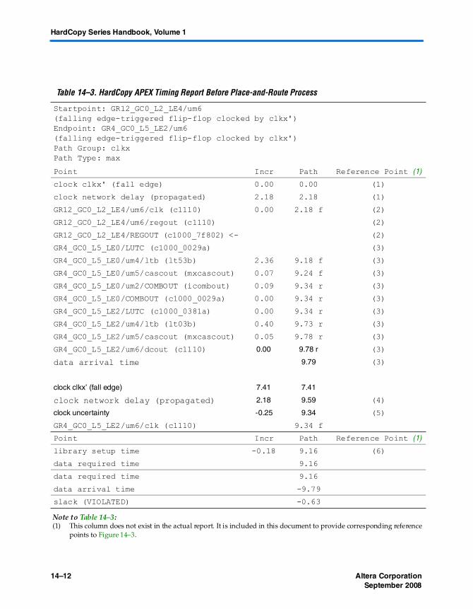
Table 14–3 shows the timing report for a path in a HardCopy APEX design that contains a high fan-out signal before the place-and-route process. Table 14–4 shows the timing report for a path that contains a high fan-out signal after the place-and-route process. Before the place-and-route process, there is a large delay on the high fan-out net driven by the pin GR12_GC0_L2_LE4/REGOUT. This delay is due to the large capacitive load that the pin has to drive. Figure 14–3 shows the timing report information.
14–12 Altera CorporationSeptember 2008
HardCopy Series Handbook, Volume 1
Table 14–3. HardCopy APEX Timing Report Before Place-and-Route Process
Startpoint: GR12_GC0_L2_LE4/um6(falling edge-triggered flip-flop clocked by clkx')Endpoint: GR4_GC0_L5_LE2/um6(falling edge-triggered flip-flop clocked by clkx')Path Group: clkxPath Type: max
Point Incr Path Reference Point (1)
clock clkx' (fall edge) 0.00 0.00 (1)
clock network delay (propagated) 2.18 2.18 (1)
GR12_GC0_L2_LE4/um6/clk (c1110) 0.00 2.18 f (2)
GR12_GC0_L2_LE4/um6/regout (c1110) (2)
GR12_GC0_L2_LE4/REGOUT (c1000_7f802) <- (2)
GR4_GC0_L5_LE0/LUTC (c1000_0029a) (3)
GR4_GC0_L5_LE0/um4/ltb (lt53b) 2.36 9.18 f (3)
GR4_GC0_L5_LE0/um5/cascout (mxcascout) 0.07 9.24 f (3)
GR4_GC0_L5_LE0/um2/COMBOUT (icombout) 0.09 9.34 r (3)
GR4_GC0_L5_LE0/COMBOUT (c1000_0029a) 0.00 9.34 r (3)
GR4_GC0_L5_LE2/LUTC (c1000_0381a) 0.00 9.34 r (3)
GR4_GC0_L5_LE2/um4/ltb (lt03b) 0.40 9.73 r (3)
GR4_GC0_L5_LE2/um5/cascout (mxcascout) 0.05 9.78 r (3)
GR4_GC0_L5_LE2/um6/dcout (c1110) 0.00 9.78 r (3)
data arrival time 9.79 (3)
clock clkx’ (fall edge) 7.41 7.41
clock network delay (propagated) 2.18 9.59 (4)
clock uncertainty -0.25 9.34 (5)
GR4_GC0_L5_LE2/um6/clk (c1110) 9.34 f
Point Incr Path Reference Point (1)
library setup time -0.18 9.16 (6)
data required time 9.16
data required time 9.16
data arrival time -9.79
slack (VIOLATED) -0.63
Note to Table 14–3:(1) This column does not exist in the actual report. It is included in this document to provide corresponding reference
points to Figure 14–3.
Altera Corporation 14–13September 2008
Importance of Timing Constraints
Figure 14–3 shows the circuit that Table 14–3 static timing analysis report describes.
Figure 14–3. Circuit That Has a Setup-Time Violation
1 The timing numbers in this report are based on pre-layout estimated delays.
Placing the values from the static timing analysis report into the set-up time slack equation, results in the following.
This result shows that there is negative slack for this path, meaning that there is a setup-time violation of 0.63 ns.
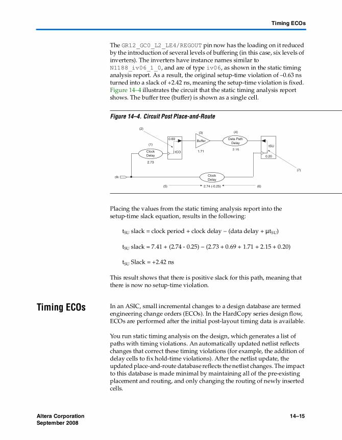
After place-and-route, a buffer tree is constructed on the high fan-out net and the setup-time violation is fixed. Table 14–4 shows the timing report for the same path. The changes to the netlist are in bold italic type. Figure 14–4 shows more information on this timing report.
14–14 Altera CorporationSeptember 2008
HardCopy Series Handbook, Volume 1
Table 14–4. HardCopy APEX Timing Report After the Place-and-Route Process Startpoint: GR12_GC0_L2_LE4/um6(falling edge-triggered flip-flop clocked by clkx')Endpoint: GR4_GC0_L5_LE2/um6(falling edge-triggered flip-flop clocked by clkx')Path Group: clkxPath Type: maxPoint Incr Path Reference Point (1)
clock clkx' (fall edge) 0.00 0.00
clock network delay (propagated) 2.73 2.73 (1)
GR12_GC0_L2_LE4/um6/clk (c1110) 0.00 2.73 f (2)
GR12_GC0_L2_LE4/um6/regout (c1110) 0.69 * 3.42 r (2)
GR12_GC0_L2_LE4/REGOUT (c1000_7f802) <- 0.00 3.42 r (2)
N1188_iv06_1_0/Z (iv06) 0.06 * 3.49 f (3)
N1188_iv06_2_0/Z (iv06) 0.19 * 3.68 r (3)
N1188_iv06_3_0/Z (iv06) 0.12 * 3.80 f (3)
N1188_iv06_4_0/Z (iv06) 0.10 * 3.90 r (3)
N1188_iv06_5_0/Z (iv06) 0.08 * 3.97 f (3)
N1188_iv06_6_2/Z (iv06) 1.16 * 5.13 r (3)
GR4_GC0_L5_LE0/LUTC (c1000_0029a) 0.00 5.13 r (4)
GR4_GC0_L5_LE0/um4/ltb (lt53b) 1.55 * 6.68 f (4)
GR4_GC0_L5_LE0/um5/cascout (mxcascout) 0.06 * 6.74 f (4)
GR4_GC0_L5_LE0/um2/COMBOUT (icombout) 0.09 * 6.84 r (4)
GR4_GC0_L5_LE0/COMBOUT (c1000_0029a) 0.00 6.84 r (4)
GR4_GC0_L5_LE2/LUTC (c1000_0381a) 0.00 6.84 r (4)
GR4_GC0_L5_LE2/um4/ltb (lt03b) 0.40 * 7.24 r (4)
GR4_GC0_L5_LE2/um5/cascout (mxcascout) 0.05 * 7.28 r (4)
GR4_GC0_L5_LE2/um6/dcout (c1110) 0.00 * 7.28 r (4)
data arrival time 7.28 (4)
Point Incr Path Reference Point (1)
clock clkx' (fall edge) 7.41 7.41
clock network delay (propagated) 2.74 10.15 (5)
clock uncertainty -0.25 9.90 (6)
GR4_GC0_L5_LE2/um6/clk (c1110) 9.90 f
library setup time -0.20 * 9.70 (7)
data required time 9.70
data required time 9.70
data arrival time -7.28
slack (MET) 2.42
Note to Table 14–4:(1) This column does not exist in the actual report. It is included in this document to provide corresponding reference
points to Figure 14–4.
Altera Corporation 14–15September 2008
Timing ECOs
The GR12_GC0_L2_LE4/REGOUT pin now has the loading on it reduced by the introduction of several levels of buffering (in this case, six levels of inverters). The inverters have instance names similar to N1188_iv06_1_0, and are of type iv06, as shown in the static timing analysis report. As a result, the original setup-time violation of –0.63 ns turned into a slack of +2.42 ns, meaning the setup-time violation is fixed. Figure 14–4 illustrates the circuit that the static timing analysis report shows. The buffer tree (buffer) is shown as a single cell.
Figure 14–4. Circuit Post Place-and-Route
Placing the values from the static timing analysis report into the setup-time slack equation, results in the following:
This result shows that there is positive slack for this path, meaning that there is now no setup-time violation.
Timing ECOs In an ASIC, small incremental changes to a design database are termed engineering change orders (ECOs). In the HardCopy series design flow, ECOs are performed after the initial post-layout timing data is available.
You run static timing analysis on the design, which generates a list of paths with timing violations. An automatically updated netlist reflects changes that correct these timing violations (for example, the addition of delay cells to fix hold-time violations). After the netlist update, the updated place-and-route database reflects the netlist changes. The impact to this database is made minimal by maintaining all of the pre-existing placement and routing, and only changing the routing of newly inserted cells.
(7)
(6)
clk
(5) 2.74 (-0.25)
BufferData Path
Delay
ClockDelay
1.71 2.15
0.20
tSU
0.69
tCO
(2)
(1)
ClockDelay
2.73
(3) (4)
14–16 Altera CorporationSeptember 2008
HardCopy Series Handbook, Volume 1
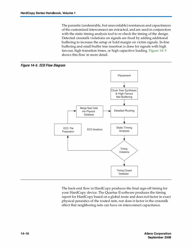
The parasitic (undesirable, but unavoidable) resistances and capacitances of the customized interconnect are extracted, and are used in conjunction with the static timing analysis tool to re-check the timing of the design. Detected crosstalk violations on signals are fixed by adding additional buffering to increase the setup or hold margin on victim signals. In-line buffering and small buffer tree insertion is done for signals with high fan-out, high transition times, or high capacitive loading. Figure 14–5 shows this flow in more detail.
Figure 14–5. ECO Flow Diagram
The back-end flow in HardCopy produces the final sign-off timing for your HardCopy device. The Quartus II software produces the timing report for HardCopy based on a global route and does not factor in exact physical parasitics of the routed nets, nor does it factor in the crosstalk effect that neighboring nets can have on interconnect capacitance.
Timing Closed Database
Clock Tree Synthesis & High FanoutNet Buffering
Placement
Static TimingAnalysis
Detailed RoutingMerge New Cells into Physical Database
ECO File Preparation
Timing Violations
ECO Iterations
Altera Corporation 14–17September 2008
Conclusion
Conclusion It is critical that you fully constrain your HardCopy series design for timing. Although HardCopy series devices are functionally equivalent to their FPGA prototype companion, they have inevitable timing differences. Fully constrained timing paths are a cornerstone of designing for HardCopy series devices.
Consult with Altera if you have questions on what areas to concentrate your efforts in to achieve timing closure within the Quartus fitter for HardCopy design submission.
Document Revision History
Table 14–5 shows the revision history for this chapter.
Table 14–5.Document Revision History (Part 1 of 2)
Date and Document Version Changes Made Summary of Changes
September 2008, v2.4
Updated chapter number and metadata. —
June 2007, v2.3 Minor text edits. —
December 2006 v2.2
● Minor updates for the Quartus II software version 6.1.0● Moved Checking the HardCopy Series Device Timing
section to Chapter 7
A minor update to the chapter, due to changes in
the Quartus II software version 6.1 release; also, Checking the HardCopy
Series Device Timing section moved to
Chapter 7.
March 2006 Formerly chapter 17; no content change. —
October 2005 v2.1 ● Moved Chapter 16 Back-End Timing Closure for Hardcopy Series Devices to Chapter 17 in HardCopy Series Device Handbook release 3.2
● Updated graphics● Minor edits
—
14–18 Altera CorporationSeptember 2008
HardCopy Series Handbook, Volume 1
January 2005v2.0
● Chapter title changed to Back-End Timing Closure for HardCopy Series Devices.
● Sizes of silicon technology updated in “Timing Closure” on page 17–2.
● HardCopy® Stratix® and HardCopy APEX™ equivalence to their respective FPGA is updated on page 17–2.
● Stratix II migration added.● Updated Table 17–2 on page 17–12.● Updated last paragraph in “Timing ECOs” on
page 17–18.
—
June 2003v1.0
Initial release of Chapter 17, Back-End Timing Closure for HardCopy Series Devices.
—
Table 14–5.Document Revision History (Part 2 of 2)
Date and Document Version Changes Made Summary of Changes