280
June 2002 DAC02 – Physical Chip Implementation 1 Section IV: Timing Closure Techniques
| Date post: | 18-Mar-2018 |
| Category: |
Documents |
| Upload: | nguyentruc |
| View: | 221 times |
| Download: | 0 times |
June 2002 DAC02 – Physical Chip Implementation 1
Section IV: Timing Closure Techniques

June 2002 DAC02 - Physical Chip Implementation 2
IBM Contributions to this presentation include:n T.J. Watson Research Centern Austin Research Labn ASIC Design Centersn EDA Organization
* For more detailed information see references atthe end of this presentation, which include a widevariety of IBM and External publications covering theseareas.
June 2002 DAC02 - Physical Chip Implementation 3
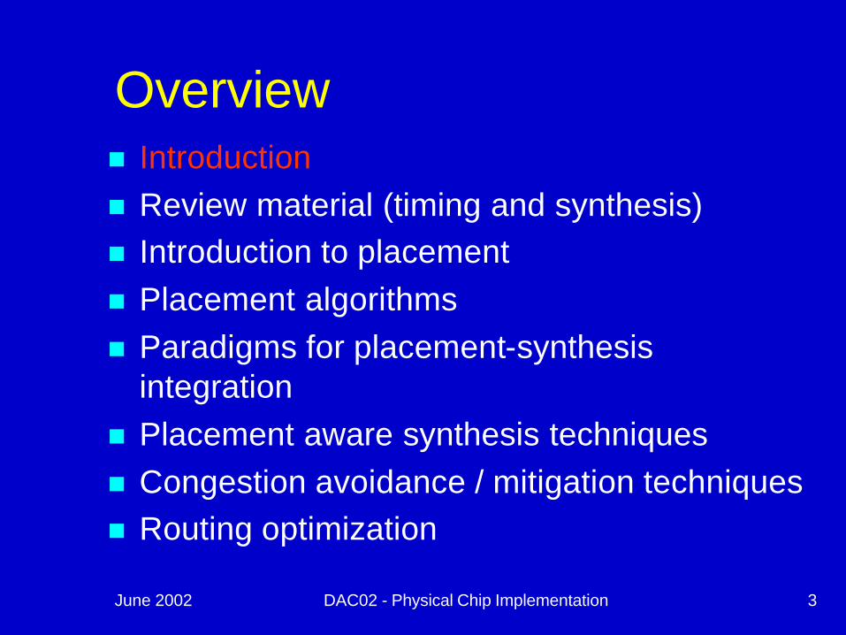
Overviewn Introductionn Review material (timing and synthesis)n Introduction to placementn Placement algorithmsn Paradigms for placement-synthesis
integrationn Placement aware synthesis techniquesn Congestion avoidance / mitigation techniquesn Routing optimization

June 2002 DAC02 - Physical Chip Implementation 4
Timing Closuren Many aspects of a design contribute to performance,
power, and densityuArchitecture / Logic ImplementationuPD Design Style (Flat, Hierarchical, etc)uClocking Paradigm / Test / Circuit Familyu Floor Plan / Synthesis / Placement / Routing
n Design Automation for timing closure is more significant than ever beforeuDesigns are largeruWires are longer, invalidating statistical synthesis
models, and requiring lots of buffersuCycle times are more aggressive

June 2002 DAC02 - Physical Chip Implementation 5
Design Automation Tools are Individually Maturen Timing analysisn Synthesis / Technology mappingn Placement / Routingn Floor Planningn Extraction / Analysis
June 2002 DAC02 - Physical Chip Implementation 6
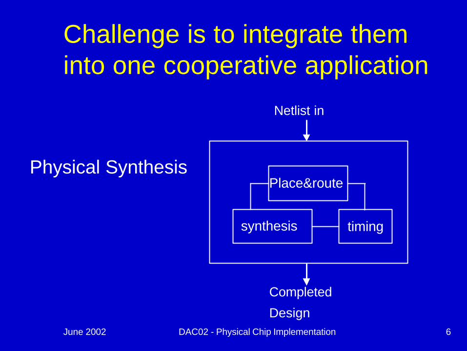
Physical SynthesisPlace&route
synthesis timing
Challenge is to integrate them into one cooperative application
Netlist in
Completed
Design
June 2002 DAC02 - Physical Chip Implementation 7
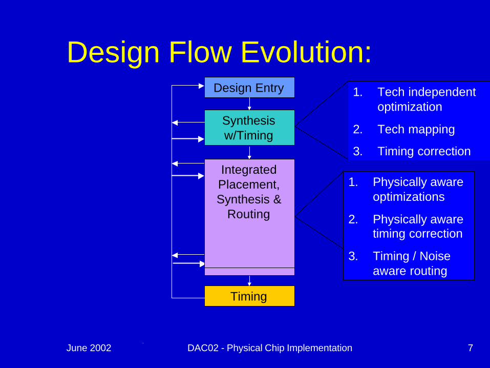
Design Flow Evolution:Design Entry
Synthesis w/Timing
Place
Route
Timing
1. Tech independent optimization
2. Tech mapping
3. Timing correctionTiming driven
placement Timing Driven
Placement plus
Automatic Post
placement tuning
Integrated Placement
and Synthesis
Integrated Placement, Synthesis &
Routing
1. Physically aware optimizations
2. Physically aware timing correction
3. Timing / Noise aware routing

June 2002 DAC02 - Physical Chip Implementation 8
Purpose of this Section:
n Provide users with an intuitive feel of the inner workings of the major timing closure tools
n Demonstrate the advancements in timing closure tools technology via example designs
n Explore a variety of significant design choices
June 2002 DAC02 - Physical Chip Implementation 9
What you should expect:
n High level concepts presented are generally applicable across a wide range of tools / methodologies (ie: not IBM specific)
n Specific tool internals used in this tutorial are taken from IBM tools. They should provide a reasonable “feel” as to how things are done in the industry.
June 2002 DAC02 - Physical Chip Implementation 10
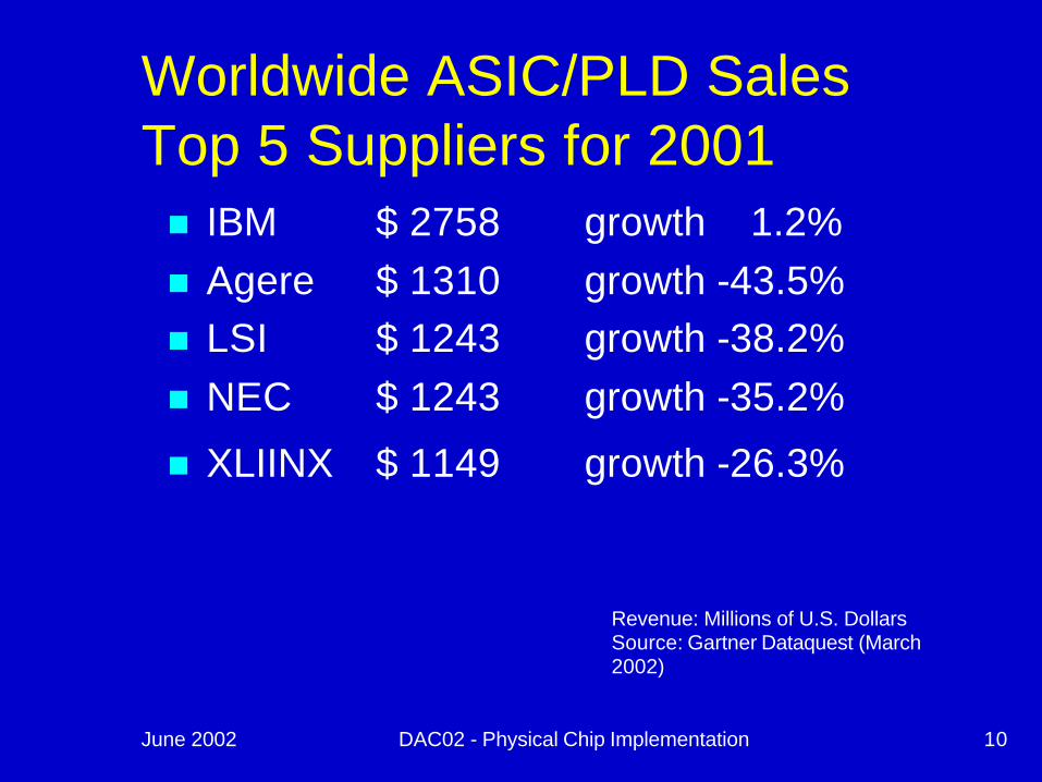
Worldwide ASIC/PLD SalesTop 5 Suppliers for 2001n IBM $ 2758 growth 1.2%n Agere $ 1310 growth -43.5%n LSI $ 1243 growth -38.2% n NEC $ 1243 growth -35.2%
n XLIINX $ 1149 growth -26.3%
Revenue: Millions of U.S. DollarsSource: Gartner Dataquest (March 2002)
June 2002 DAC02 - Physical Chip Implementation 11
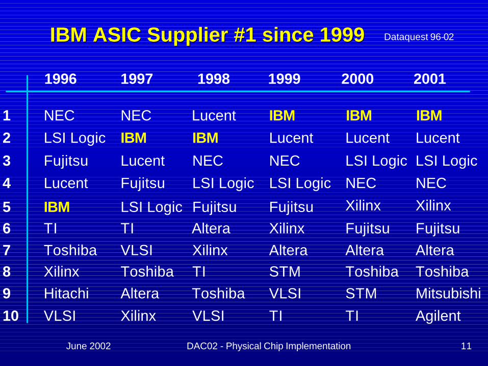
IBM ASIC Supplier #1 since 1999IBM ASIC Supplier #1 since 1999
NEC
Lucent
LSI Logic
IBM
VLSI
Xilinx
TI
Fujitsu
Toshiba
Hitachi Altera
NEC
Lucent
LSI Logic
IBM
VLSI
Xilinx
TI
Fujitsu
Toshiba
Altera
NEC
Lucent
LSI Logic
IBM
VLSI
XilinxTI
Fujitsu
Toshiba
Altera
NEC
Lucent
LSI Logic
IBM
VLSI
Xilinx
TI
Fujitsu
STM
NEC
Lucent
LSI Logic
IBM1
2
3
4
56789
10
1996 1997 1998 1999 2000
AlteraToshiba
Xilinx
TI
Fujitsu
STM
NEC
Lucent
LSI Logic
IBM
AlteraToshiba
Xilinx
Agilent
Fujitsu
Mitsubishi
2001
Dataquest 96-02

June 2002 DAC02 - Physical Chip Implementation 12
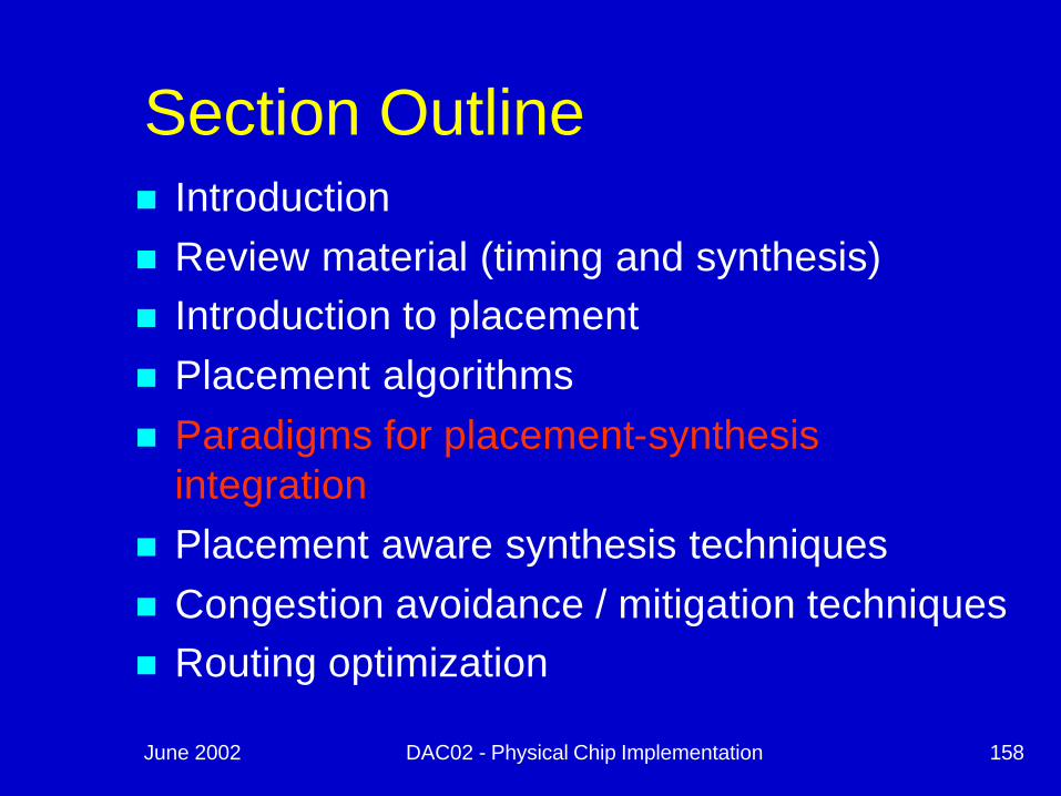
Section Outlinen Introductionn Review material (timing and synthesis)n Introduction to placementn Placement algorithmsn Paradigms for placement-synthesis
integrationn Placement aware synthesis techniquesn Congestion avoidance / mitigation techniquesn Routing optimization
June 2002 DAC02 - Physical Chip Implementation 13
Static Timing Analysis

June 2002 DAC02 - Physical Chip Implementation 14
Timing Analysis Basics:Why static timing since simulation is more accurate?
c=0 c=1b=0 a-z delay1 a-z delay2 b=1 a-z delay3 a-z delay4
Exponential explosion as possible design input states grow!
a
b
c
zHow would one calculate the worst case rising delay from a to z?
n A simple example:
n Simulation has a number of key drawbacksn requires input state vectorsn long runtimes

June 2002 DAC02 - Physical Chip Implementation 15
-Required arrival time(RAT) -- the time a signal must arrive at in order to avoid a chip fail
-Slack = Required arrival time - Arrival time– Positive slack good, negative slack bad
Definition of basic terms-Arrival time(AT) -- the time at switch a pin switches state
90
10time
vdd
slew = time90 -time10
50 AT = time50
-Slew - the rate at which a signal switches– usually difference of 10% and 90% on voltage curve
Timing Analysis Basics:

June 2002 DAC02 - Physical Chip Implementation 16
nBlock based timing:n Worst value only stored at merge pointsn Each segment is processed just once
d=2
d=1
d=5
d=3
d=2
d=1
d=3
d=3d=1
temp at=3 temp at=7
Example Problem: What is slack at PO?
Timing Analysis Basics:
at=0
at=0
at=0
at=1
at=2
at=5 at=6
at=5
at=8at=11
rat=10
Slack= -1
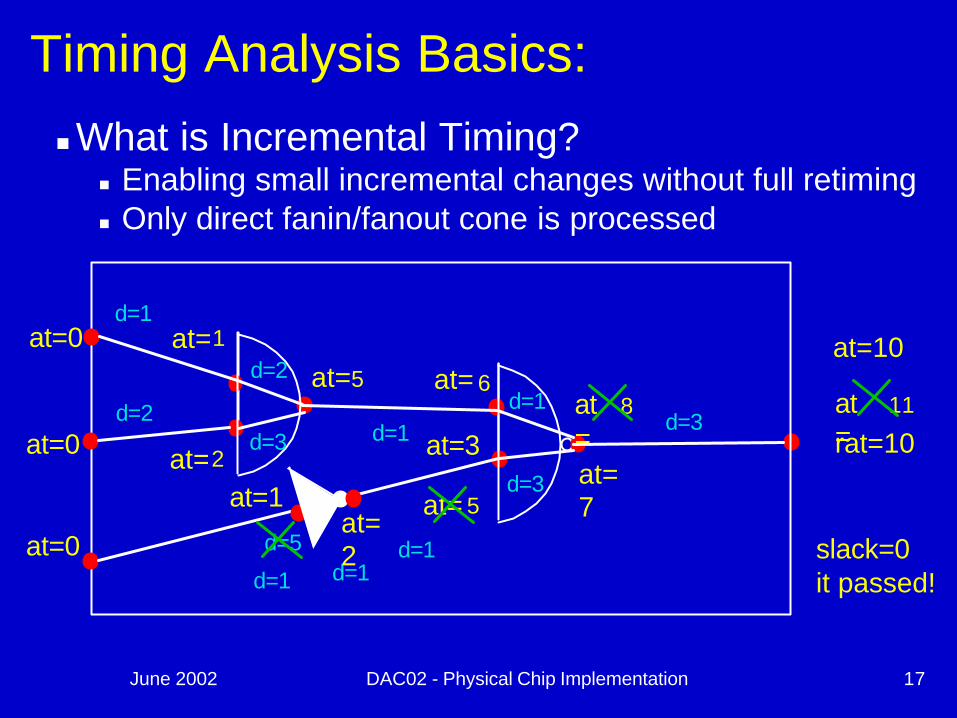
June 2002 DAC02 - Physical Chip Implementation 17
nWhat is Incremental Timing?n Enabling small incremental changes without full retimingn Only direct fanin/fanout cone is processed
at=
at=at=
at=at=
d=2
at=
at=0
at=0
rat=10at=0
at=
5
d=1
d=5
d=3
d=2
d=1
d=3
d=3d=1
2
68
5
1
11
d=1d=1d=1
at=2 slack=0
it passed!
at=3at=7
at=10
at=1
Timing Analysis Basics:

June 2002 DAC02 - Physical Chip Implementation 18
Early Mode Analysis
0=aAT
1=bAT
2=xRAT
1=xAT
121 −=−=xSL101 =−=bSL
000 =−=aSL1=yAT
0=cAT
011 =−=ySL
a
b xc
y
n Definitions change as follows– longest becomes shortest– slack = arrival - required
1 1
110 −=−=cSL
June 2002 DAC02 - Physical Chip Implementation 19
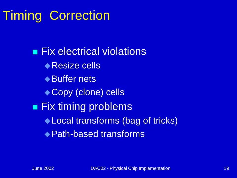
Timing Correction
n Fix electrical violationsuResize cellsuBuffer netsuCopy (clone) cells
n Fix timing problemsuLocal transforms (bag of tricks)uPath-based transforms
June 2002 DAC02 - Physical Chip Implementation 20
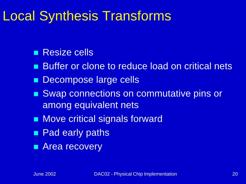
Local Synthesis Transforms
n Resize cellsn Buffer or clone to reduce load on critical netsn Decompose large cellsn Swap connections on commutative pins or
among equivalent netsn Move critical signals forwardn Pad early pathsn Area recovery
June 2002 DAC02 - Physical Chip Implementation 21
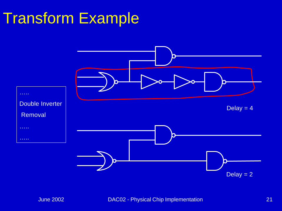
Transform Example
Delay = 4
…..
Double Inverter
Removal
…..
…..
Delay = 2

June 2002 DAC02 - Physical Chip Implementation 22
Resizing
00.010.020.030.040.05
0 0.2 0.4 0.6 0.8 1load
d
A B C
b
ad
e
f
0.2
0.2
0.3
?
b
aA
0.035
b
aC
0.026
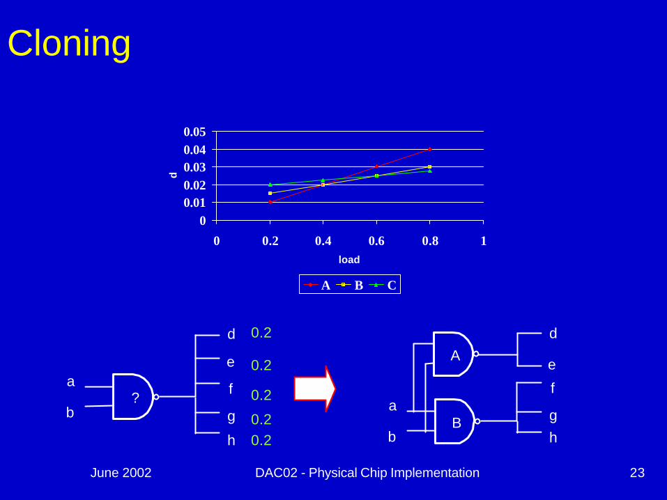
June 2002 DAC02 - Physical Chip Implementation 23
Cloning
00.010.020.030.040.05
0 0.2 0.4 0.6 0.8 1load
d
A B C
b
a
d
e
f
g
h
0.2
0.2
0.2
0.20.2
?
b
a
d
e
f
g
h
A
B
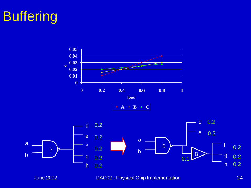
June 2002 DAC02 - Physical Chip Implementation 24
Buffering
00.010.020.030.040.05
0 0.2 0.4 0.6 0.8 1load
d
A B C
b
a
d
e
f
g
h
0.2
0.2
0.2
0.20.2
? b
a
d
e
f
g
h0.1
0.2
0.2
0.20.2
BB
0.2

June 2002 DAC02 - Physical Chip Implementation 25
Redesign Fan-in Tree
a
c
d
b eArr(b)=3
Arr(c)=1
Arr(d)=0
Arr(a)=4
Arr(e)=61
1
1
c
d
e
Arr(e)=5
1
1b1
a

June 2002 DAC02 - Physical Chip Implementation 26
Redesign Fan-out Tree
1
1
1
3
1
1
1
Longest Path = 5
1
1
1
3
1
2
Longest Path = 4Slowdown of buffer due to load

June 2002 DAC02 - Physical Chip Implementation 27
Decomposition
June 2002 DAC02 - Physical Chip Implementation 28
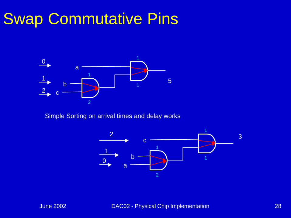
Swap Commutative Pins
2
c
ab
2
1
0 1
1
1
3
a
cb
2
1
0
1
1
2
1 5
Simple Sorting on arrival times and delay works

June 2002 DAC02 - Physical Chip Implementation 29
Move Critical Signals Forward
n Based on ATPG– linear in circuit size– Detects
redundancies efficiently
n Efficiently find wires to be added and remove.– Based on
mandatory assignments..
a
b
cd e
ab
ed
c
June 2002 DAC02 - Physical Chip Implementation 30
Section outlinen Introductionn Review material (timing and synthesis)n Introduction to placementn Placement algorithmsn Paradigms for placement-synthesis
integrationn Placement aware synthesis techniquesn Congestion avoidance / mitigation techniquesn Routing optimization

June 2002 DAC02 - Physical Chip Implementation 31
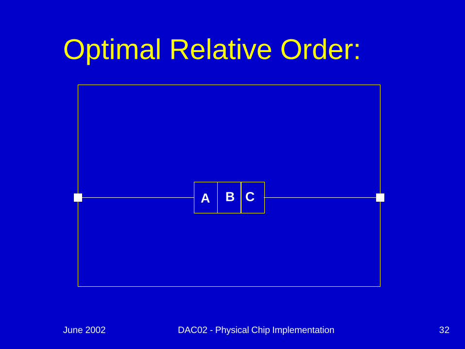
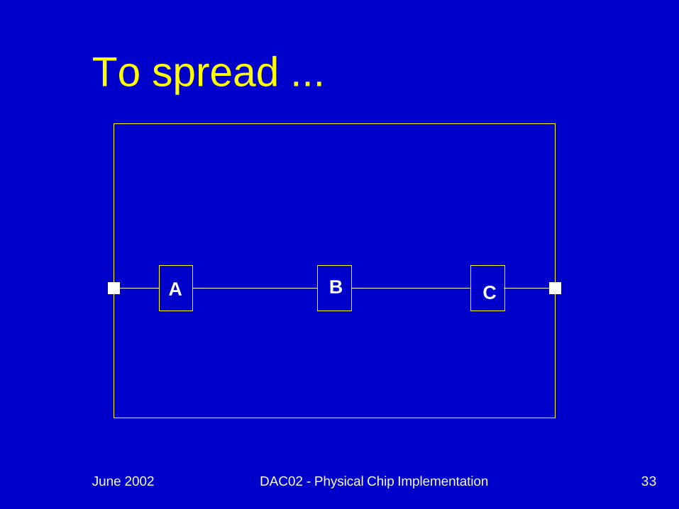
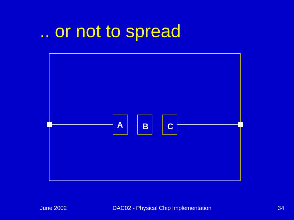
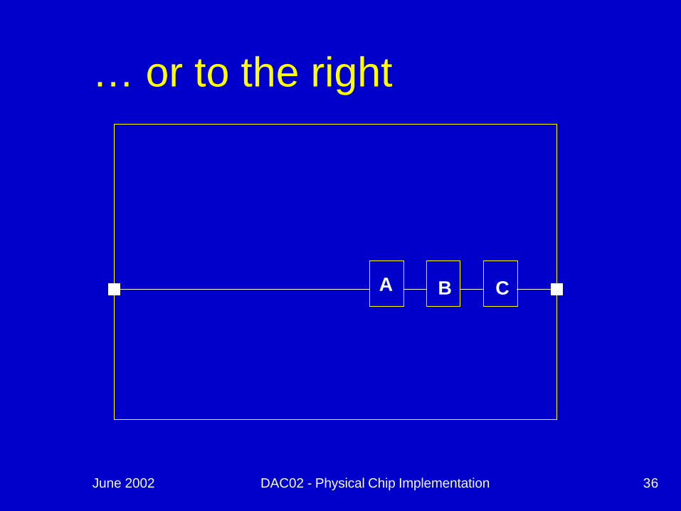
Placement Objective:n Find optimal relative ordering of cellsuminimize wire length and congestionumaximize timing slack
n Find optimal spacing of cellsu eliminate wiring congestion problemsu provide space for post placement synthesis
Fclock treesFbuffer insertionF timing correction
n Find optimal Global Position
June 2002 DAC02 - Physical Chip Implementation 32
A B C
Optimal Relative Order:
June 2002 DAC02 - Physical Chip Implementation 33
A B C
To spread ...
June 2002 DAC02 - Physical Chip Implementation 34
A B C
.. or not to spread

June 2002 DAC02 - Physical Chip Implementation 35
A B C
Place to the left
June 2002 DAC02 - Physical Chip Implementation 36
A B C
… or to the right

June 2002 DAC02 - Physical Chip Implementation 37
A B C
Optimal Relative Order:
Without “free” space the problem is dominated by order

June 2002 DAC02 - Physical Chip Implementation 38
Placement Footprints:Standard Cell:
Data Path:
IP - Floorplanning
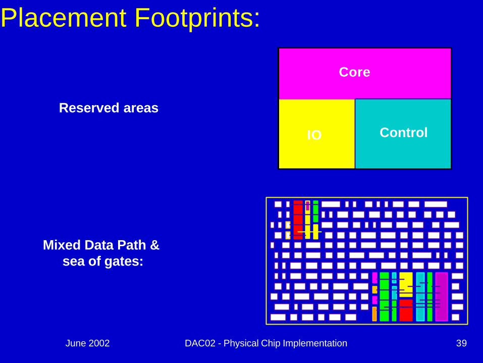
June 2002 DAC02 - Physical Chip Implementation 39
Core
ControlIO
Reserved areas
Mixed Data Path &sea of gates:
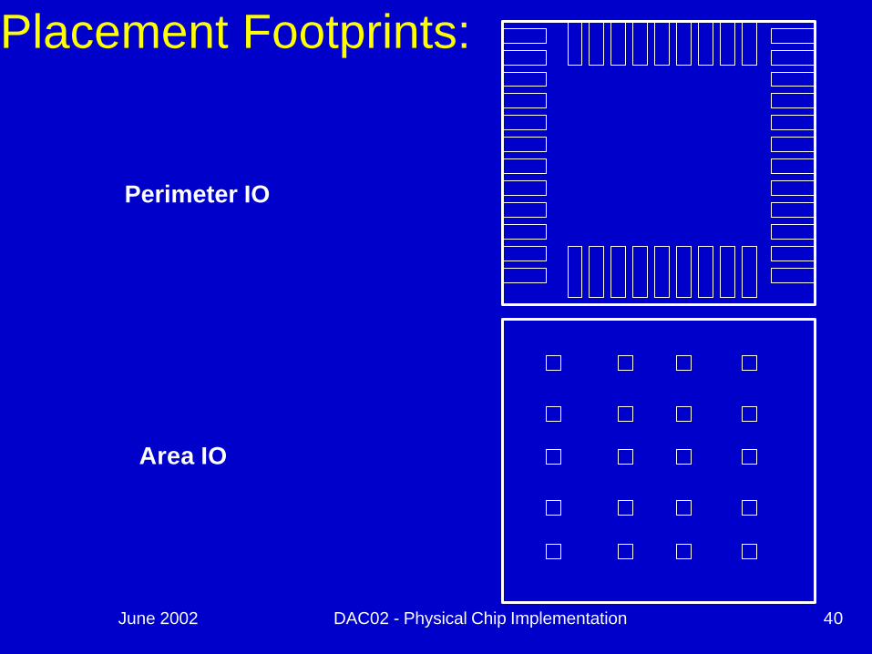
Placement Footprints:
June 2002 DAC02 - Physical Chip Implementation 40
Perimeter IO
Area IO
Placement Footprints:
June 2002 DAC02 - Physical Chip Implementation 41
Placement objectives are subject to User Constraints / Design Style:n Hierarchical Design Constraintsu pin locationu power rail u reserved layers
n Flat Design w/Floor Plan constraintsn Fixed circuitsn IO connections
June 2002 DAC02 - Physical Chip Implementation 42
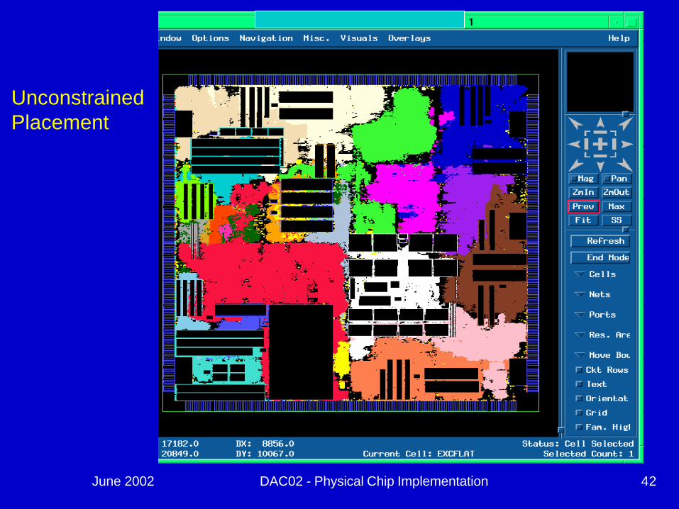
UnconstrainedPlacement
June 2002 DAC02 - Physical Chip Implementation 43
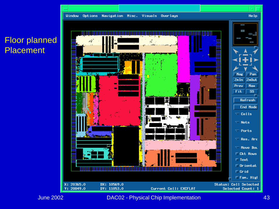
Floor plannedPlacement
June 2002 DAC02 - Physical Chip Implementation 44
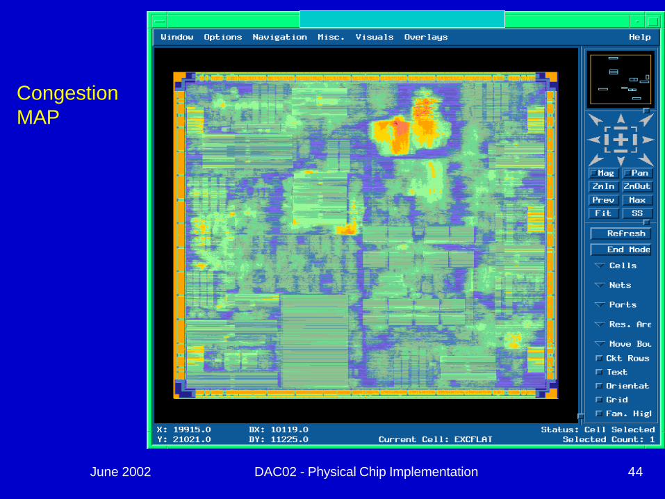
CongestionMAP

June 2002 DAC02 - Physical Chip Implementation 45
Advantages of Hierarchy
n Design is carved into smaller pieces that can be worked on in parallel (improved throughput)
n A known floor plan provides the logic design team with a large degree of placement control.
n A known floor plan provided early knowledge of long wires
n Timing closure problems can be addressed by tools, logic design, and hierarchy manipulation
n Late design changes can be done with minimal turmoil to the entire design

June 2002 DAC02 - Physical Chip Implementation 46
Disadvantages of Hierarchyn Results depend on the quality of the hierarchy. The
logic hierarchy must be designed with PD taken into account.
n Additional methodology requirements must be met to enable hierarchy. Ex. Pin assignment, Macro Abstract management, area budgeting, floor planning, timing budgets, etc
n Late design changes may affect multiple components.
n Hierarchy allows divergent methodologies n Hierarchy hinders DA algorithms. They can no
longer perform global optimizations.

June 2002 DAC02 - Physical Chip Implementation 47
Physical Synthesis FlowSynthesized NetlistWire-load Models
UnplacedPhysically “unaware” timing
Cleanup: Remove buffers, nominal power levels on gates
Initial “basic” placementFor minimal wire-length, min-cut, Steiner tree estimates, physically aware timing
Logical + Placement optimizations
Timing-driven placement w/resynthesis
For minimal netweights, based on the timing of the net
Physically aware logic optimizations
Timing Improvement
?
Placed Netlist
Yes No more

June 2002 DAC02 - Physical Chip Implementation 48
Logical + Placement Optimizations
CutBin
n Start with a placed or unplaced netlist
n Do recursive partitioningn During and following each
partition action, apply logic optimizations such asu timing correctionsu rebufferingu repoweringu cloningu pin swapping u move boxesu … etc

June 2002 DAC02 - Physical Chip Implementation 49
Section Outlinen Introductionn Review material (timing and synthesis)n Introduction to placementn Placement algorithmsn Paradigms for placement-synthesis
integrationn Placement aware synthesis techniquesn Congestion avoidance / mitigation techniquesn Routing optimization
June 2002 DAC02 - Physical Chip Implementation 50
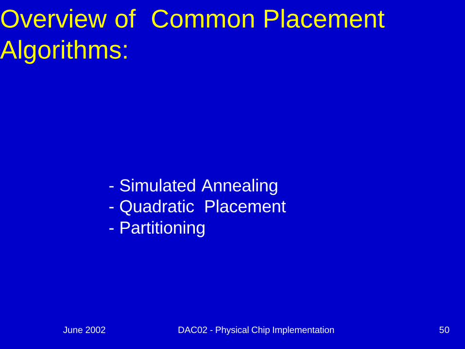
Overview of Common Placement Algorithms:
- Simulated Annealing- Quadratic Placement- Partitioning
June 2002 DAC02 - Physical Chip Implementation 51
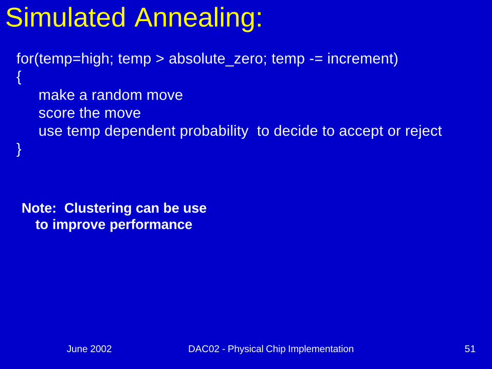
for(temp=high; temp > absolute_zero; temp -= increment){
make a random movescore the moveuse temp dependent probability to decide to accept or reject
}
Simulated Annealing:
Note: Clustering can be useto improve performance
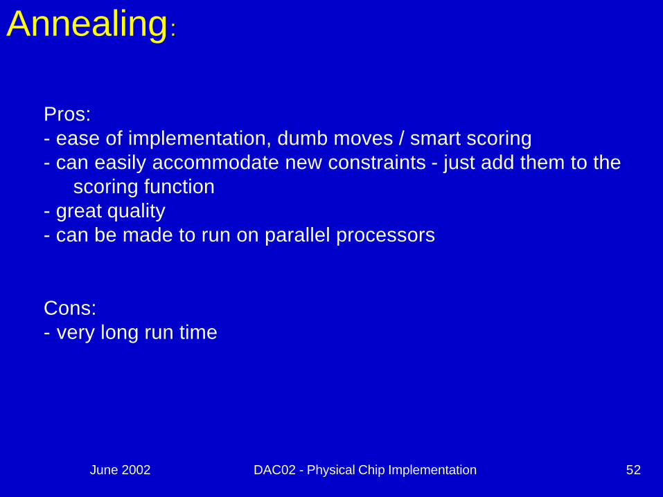
June 2002 DAC02 - Physical Chip Implementation 52
Annealing ::
Pros:- ease of implementation, dumb moves / smart scoring- can easily accommodate new constraints - just add them to the
scoring function- great quality - can be made to run on parallel processors
Cons:- very long run time
June 2002 DAC02 - Physical Chip Implementation 53
Quadratic Placement
June 2002 DAC02 - Physical Chip Implementation 54
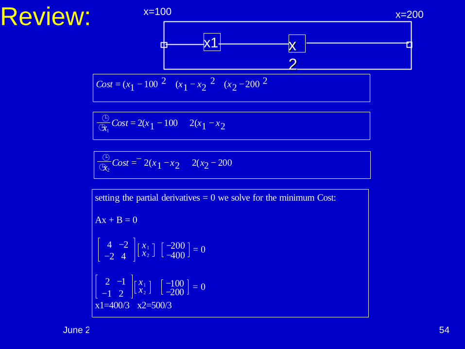
Cost = (x1 − 100)2 + (x1 − x2)2 +(x2 −200)2
¹¹x1
Cost = 2(x1 − 100)+ 2(x1 − x2)
¹¹x2
Cost =− 2(x1 −x2) + 2(x2 − 200)
setting the partial derivatives = 0 we solve for the minimum Cost:
Ax + B = 0
= 04 −2−2 4
x1x2
+ −200−400
= 02 −1−1 2
x1x2
+ −100−200
x1=400/3 x2=500/3
xx22
x1
x=100 x=200Review:
June 2002 DAC02 - Physical Chip Implementation 55
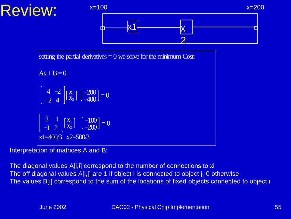
setting the partial derivatives = 0 we solve for the minimum Cost:
Ax + B = 0
= 04 −2−2 4
x1x2
+ −200−400
= 02 −1−1 2
x1x2
+ −100−200
x1=400/3 x2=500/3
xx22
x1
x=100 x=200
Interpretation of matrices A and B:
The diagonal values A[i,i] correspond to the number of connections to xiThe off diagonal values A[i,j] are 1 if object i is connected to object j, 0 otherwiseThe values B[i] correspond to the sum of the locations of fixed objects connected to object i
Review:
June 2002 DAC02 - Physical Chip Implementation 56
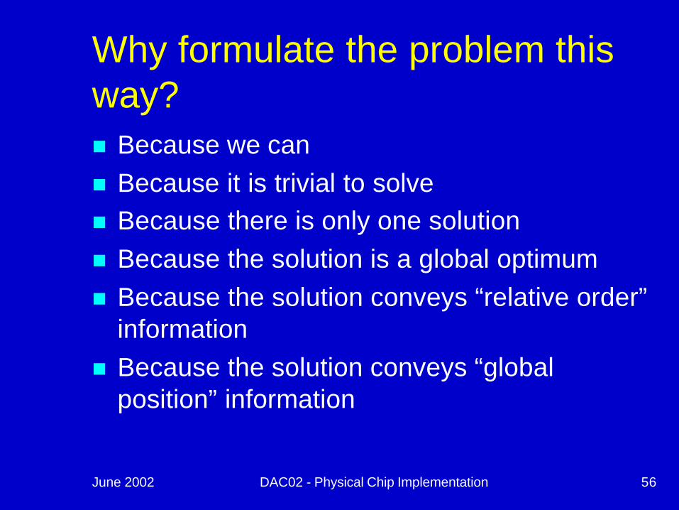
Why formulate the problem this way?n Because we cann Because it is trivial to solven Because there is only one solutionn Because the solution is a global optimumn Because the solution conveys “relative order”
informationn Because the solution conveys “global
position” information
June 2002 DAC02 - Physical Chip Implementation 57
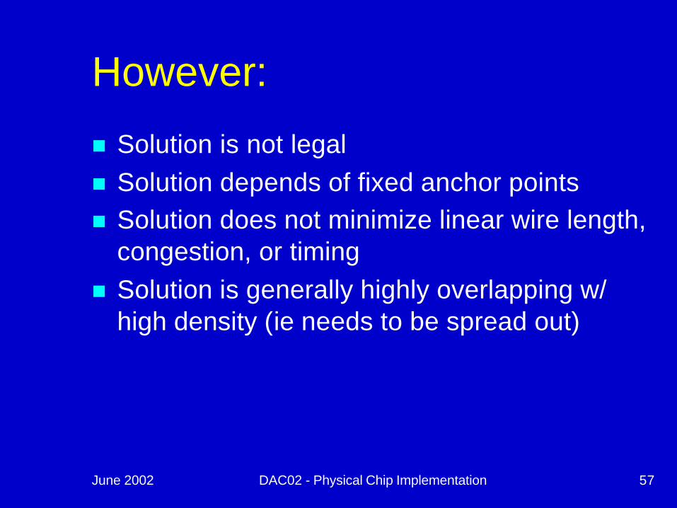
However:
n Solution is not legaln Solution depends of fixed anchor pointsn Solution does not minimize linear wire length,
congestion, or timingn Solution is generally highly overlapping w/
high density (ie needs to be spread out)

June 2002 DAC02 - Physical Chip Implementation 58
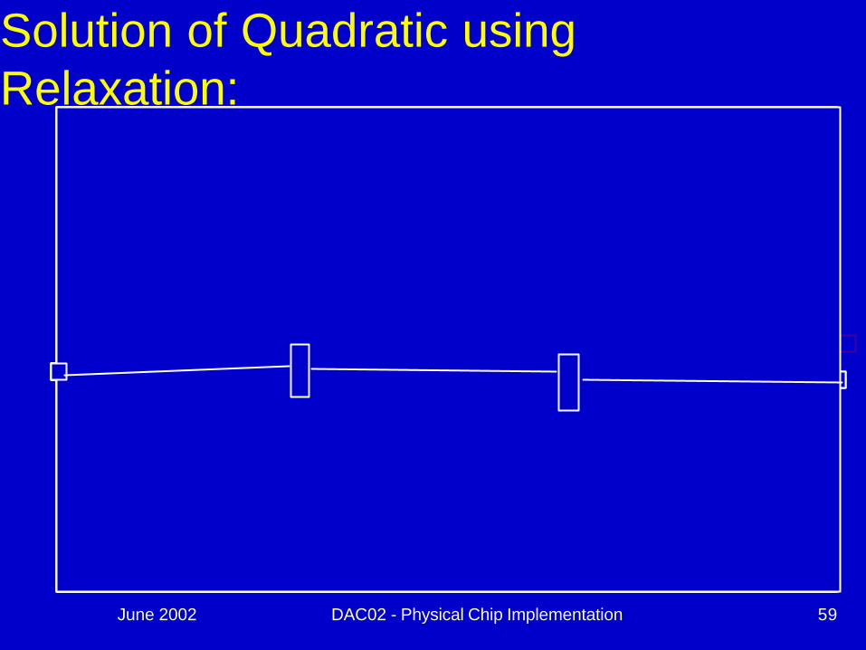
What does the solution look like?
n To get an intuitive feel for the solution, examine the relaxation method for solving Ax + B = 0
n Actual program implementation may use other solution methods (that are generally less intuitive).
June 2002 DAC02 - Physical Chip Implementation 59
Solution of Quadratic using Relaxation:
June 2002 DAC02 - Physical Chip Implementation 60
June 2002 DAC02 - Physical Chip Implementation 61
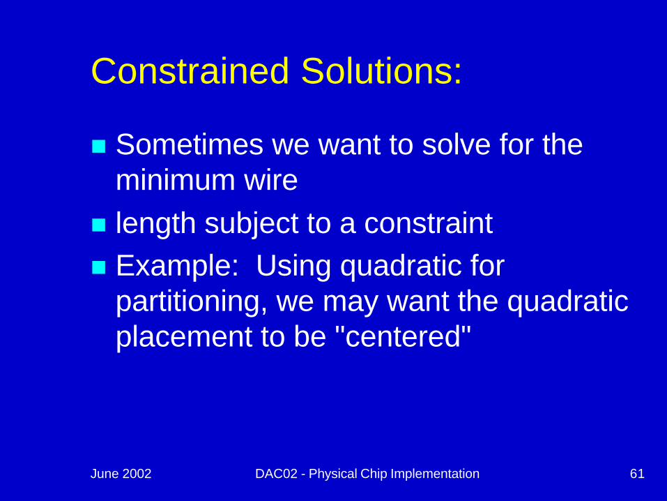
Constrained Solutions:
n Sometimes we want to solve for the minimum wire
n length subject to a constraintn Example: Using quadratic for
partitioning, we may want the quadratic placement to be "centered"
June 2002 DAC02 - Physical Chip Implementation 62

June 2002 DAC02 - Physical Chip Implementation 63
June 2002 DAC02 - Physical Chip Implementation 64
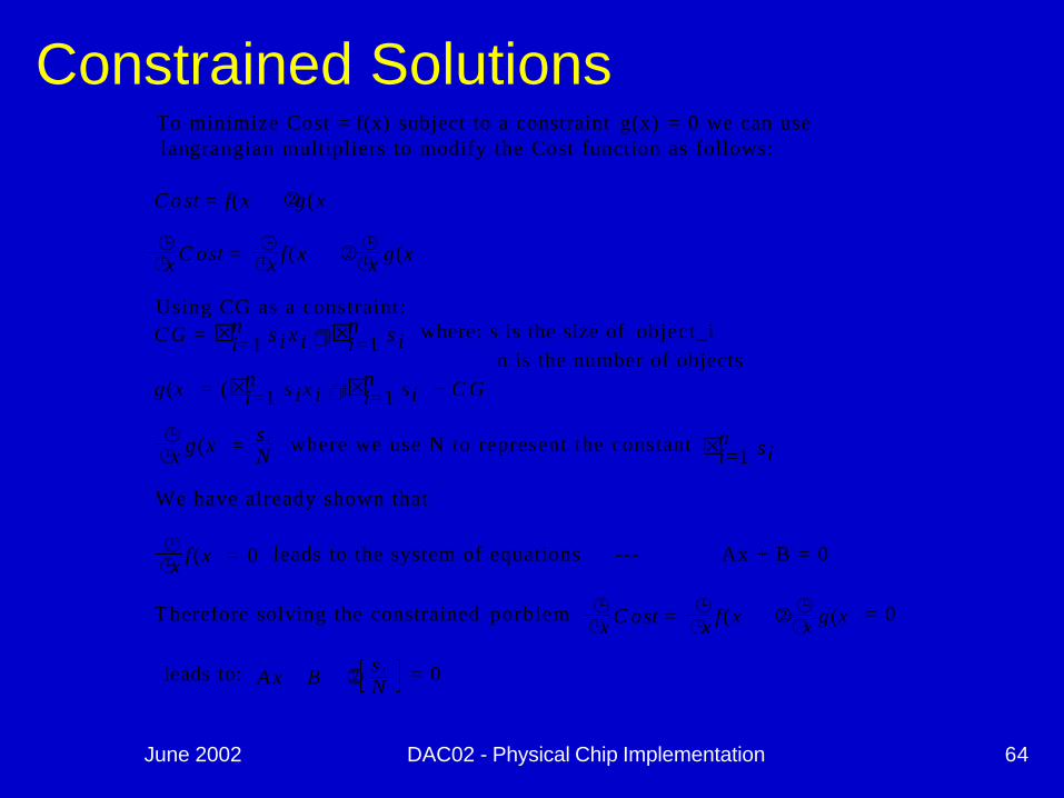
To minimize Cost = f(x) subject to a constraint g(x) = 0 we can use langrangian multipliers to modify the Cost function as follows:
C o st = f(x) + 2g(x)
¹¹x C ost = ¹
¹x f(x) + 2¹¹x g(x)
Using CG as a constraint: where: s is the size of object_i C G = Si= 1
n s i x i +Si=1n s i
n is the number of objects g(x ) = (Si=1
n s ix i +Si=1n si ) − C G
where we use N to represent the constant ¹¹x g(x) = s i
N Si=1n si
We have already shown that
leads to the system of equations --- Ax + B = 0¹¹x f(x) = 0
T herefore solving the constrained porblem = 0 ¹¹x C ost = ¹
¹x f(x) + 2¹¹x g(x) leads to: = 0A x + B + 2 s i
N
Constrained Solutions

June 2002 DAC02 - Physical Chip Implementation 65
To solve Ax + B + = 0 we could use a packaged solver and add the 2 s i
N additional unknown and equation to our matricies and 2 CG =Si=1
n s ix i +N solve.
Here is an alternative way to solve the system:
by substitution we let x = x u+2x l where is the unconstrained solution (ie the solution to Ax + B = 0)x u
Assuming we can solve the unconstrain ed problem, is known.x u
By substitution we get:
A(x u + 2x l) + B + 2 s i
N = 0
which becomes:
or A2x l + 2 s i
N = 0 Ax l + s i
N = 0
Constrained Solutions (cont):

June 2002 DAC02 - Physical Chip Implementation 66
We need to solve: A x l + s i
N = 0
Note: The A matr ix is the same as the A matr ix for the unconstrained solut ion. Since the A matrix is the net l is t c o n nectivity specification, we have A.
The B matrix here is instead of the sum of fixed location connects.s i
N
In t repre ta t ion:
The solut ion to can be obtained by modifying the original netlist A x l + s i
N = 0 and placement such that :
1.) All f ixed objects are moved x = 02.) A constant force vector is applied to each object . The constant force vector for the i’th o b ject has magnitude s i
N
Then use the same solver as was used to solve Ax + B = 0
Constrained Solutions (cont):

June 2002 DAC02 - Physical Chip Implementation 67
We also need to solve for 2
From the CG relationship and we get:x=xu+2xl
where (ie total size)CG=Si=0n si(xui +2xli
)+N N=Si=0n si
since we have solved for and the only unkown is xu xl 2
we get:
2=NCG−Si=0
n sixui
Si=0n sixli
Constrained Solutions (cont):

June 2002 DAC02 - Physical Chip Implementation 68
To minimize f(x) ( the wl squared cost function) subject to a CG constraint we do thefol lowing:
1.) Solve for by solving using relaxation or some other methodx u A x u + B = 0
2.) Solve for as follows: x l A x l + s i
N = 0 - Move all fixed objects to locat ion=0
- Add a constant force vector to each object. The constant force vector for the i’th ob ject has magnitude s i
N - Using rela xation or some other method, solve for x l
3.) Solve for using 2 2=N C G −Si= 0
n s i x u i
Si= 0n s ix l i
4.) Compute the final placement using x = x u + 2x l
Constrained Solutions (summary):

June 2002 DAC02 - Physical Chip Implementation 69
xx22
x=100 x=200
Force CG to 150s=100
From the previous example we know that the solution to:
Axu + B = 0
x =133.33166.67
with this solution the CG is at (ie not 150)(10&133.33)+(100&166.67)110 = 163.64
Now we need to solve:
which is the same as solving -> Axl + s i
N = 0 Axl +00 + s i
N = 0
Recall that the B matrix represents the position of fixed objects. So, this equationrepresents the solution to:
x1s=10
x1x2
10/110
100/110x = 0
Review:
June 2002 DAC02 - Physical Chip Implementation 70
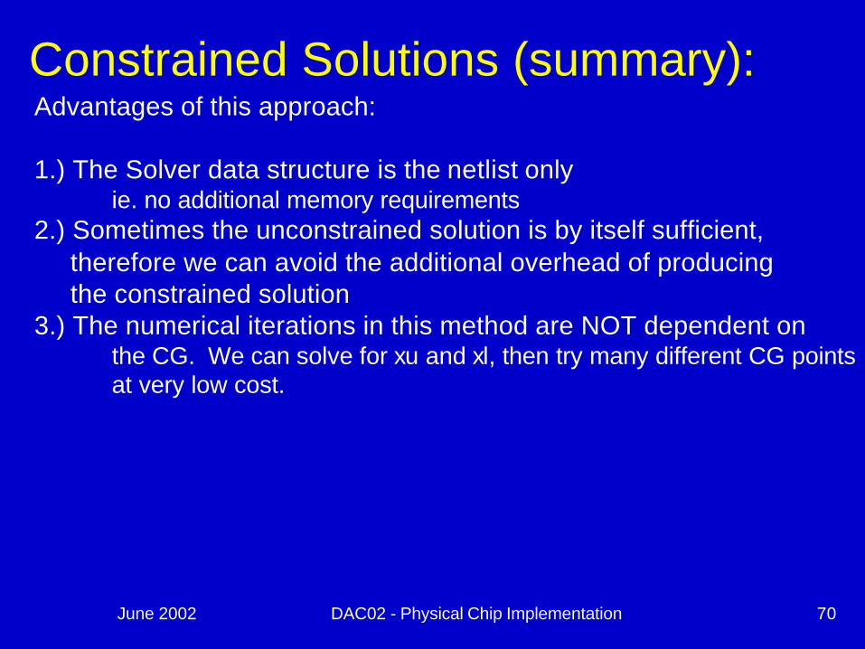
Constrained Solutions (summary):Advantages of this approach:
1.) The Solver data structure is the netlist onlyie. no additional memory requirements
2.) Sometimes the unconstrained solution is by itself sufficient,therefore we can avoid the additional overhead of producingthe constrained solution
3.) The numerical iterations in this method are NOT dependent onthe CG. We can solve for xu and xl, then try many different CG pointsat very low cost.
June 2002 DAC02 - Physical Chip Implementation 71
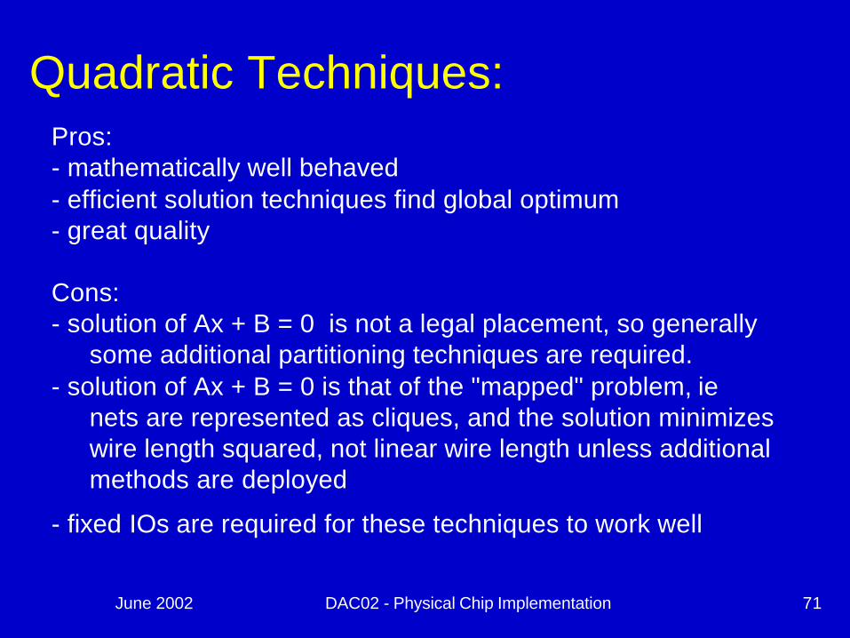
Quadratic Techniques:Pros:- mathematically well behaved- efficient solution techniques find global optimum- great quality
Cons:- solution of Ax + B = 0 is not a legal placement, so generally
some additional partitioning techniques are required.- solution of Ax + B = 0 is that of the "mapped" problem, ie
nets are represented as cliques, and the solution minimizes wire length squared, not linear wire length unless additionalmethods are deployed
- fixed IOs are required for these techniques to work well
June 2002 DAC02 - Physical Chip Implementation 72
Partitioning
June 2002 DAC02 - Physical Chip Implementation 73
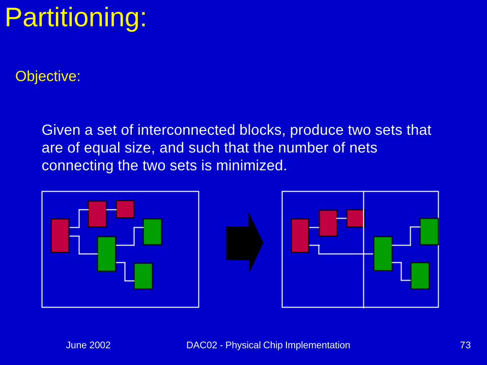
Partitioning:
Objective:
Given a set of interconnected blocks, produce two sets thatare of equal size, and such that the number of nets connecting the two sets is minimized.
June 2002 DAC02 - Physical Chip Implementation 74
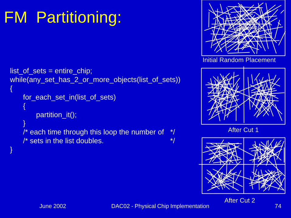
FM Partitioning:
Initial Random Placement
After Cut 1
After Cut 2
list_of_sets = entire_chip;while(any_set_has_2_or_more_objects(list_of_sets)){
for_each_set_in(list_of_sets){
partition_it();}/* each time through this loop the number of *//* sets in the list doubles. */
}

June 2002 DAC02 - Physical Chip Implementation 75
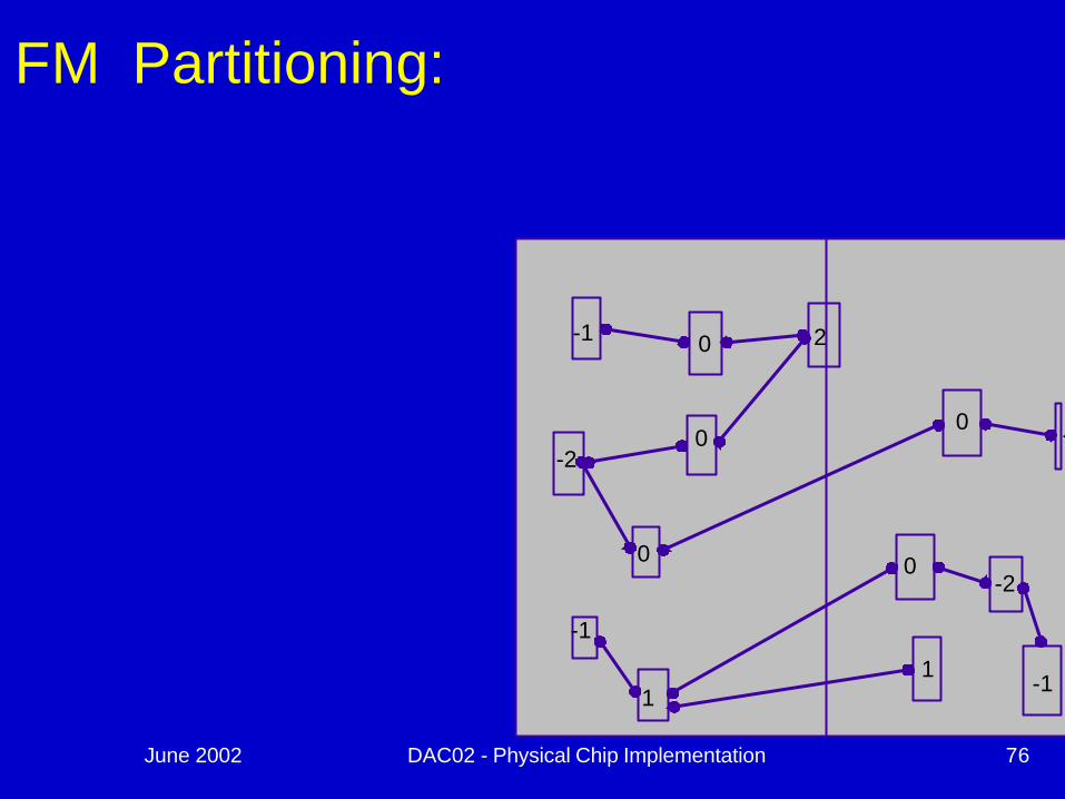
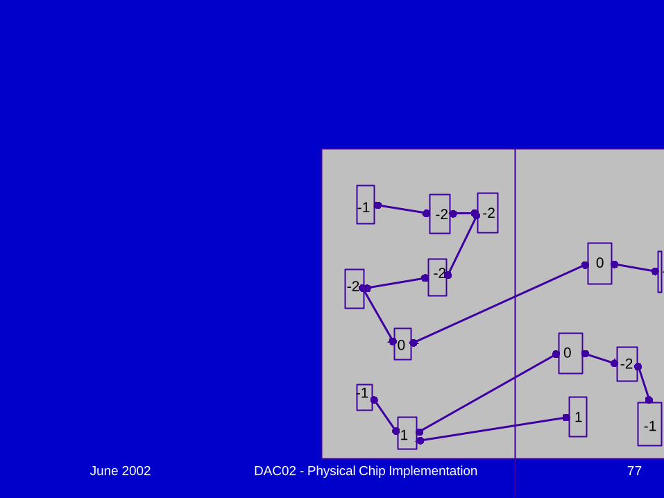
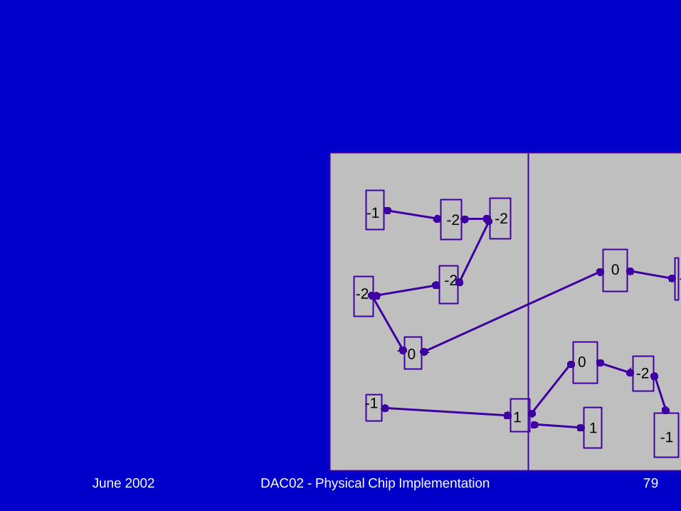
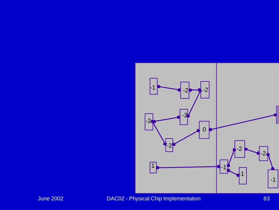
FM Partitioning:
-1
-2
-1
1
0
0
0
2
0
0
1
-
-1
-2
- each object is assigned a gain
- objects are put into a sortedgain list
- the object with the highest gainfrom the smaller of the two sidesis selected and moved.
- the moved object is "locked"- gains of "touched" objects are
recomputed- gain lists are resorted
Object Gain: The amount of change in cut crossingsthat will occur if an object is moved fromits current partition into the other partition
Moves are made based on object gain.
June 2002 DAC02 - Physical Chip Implementation 76
-1
-2
-1
1
0
0
0
2
0
0
1
-
-1
-2
FM Partitioning:
June 2002 DAC02 - Physical Chip Implementation 77
-1
-2
-1
1
0
-2
-20
0
1
-
-1
-2
-2

June 2002 DAC02 - Physical Chip Implementation 78
-1
-2
-1
1
0
-2
-20
0
1
-
-1
-2
-2
June 2002 DAC02 - Physical Chip Implementation 79
-1
-2
-11
0
-2
-20
0
1
-
-1
-2
-2

June 2002 DAC02 - Physical Chip Implementation 80
-1
-2
1 -1
0
-2
-20
-2
-1
-
-1
-2
-2

June 2002 DAC02 - Physical Chip Implementation 81
-1
-2
1 -1
0
-2
-2 0
-2
-1
-
-1
-2
-2

June 2002 DAC02 - Physical Chip Implementation 82
-1
-2
1 -1
0
-2
-20
-2
-1
-
-1
-2
-2
June 2002 DAC02 - Physical Chip Implementation 83
-1
-2
1 -1
-2
-2
-2
0
-2
-1
1
-1
-2
-2
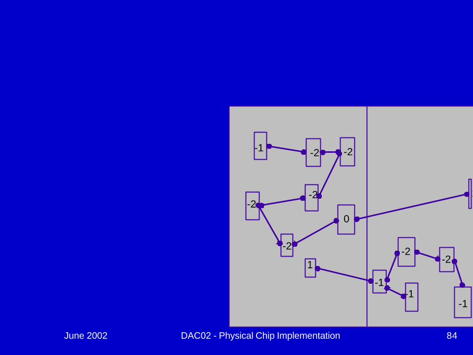
June 2002 DAC02 - Physical Chip Implementation 84
-1
-2
1
-1
-2
-2
-2
0
-2
-1
1
-1
-2
-2

June 2002 DAC02 - Physical Chip Implementation 85
-1
-2
1
-1
-2
-2
-2
0
-2
-1
1
-1
-2
-2
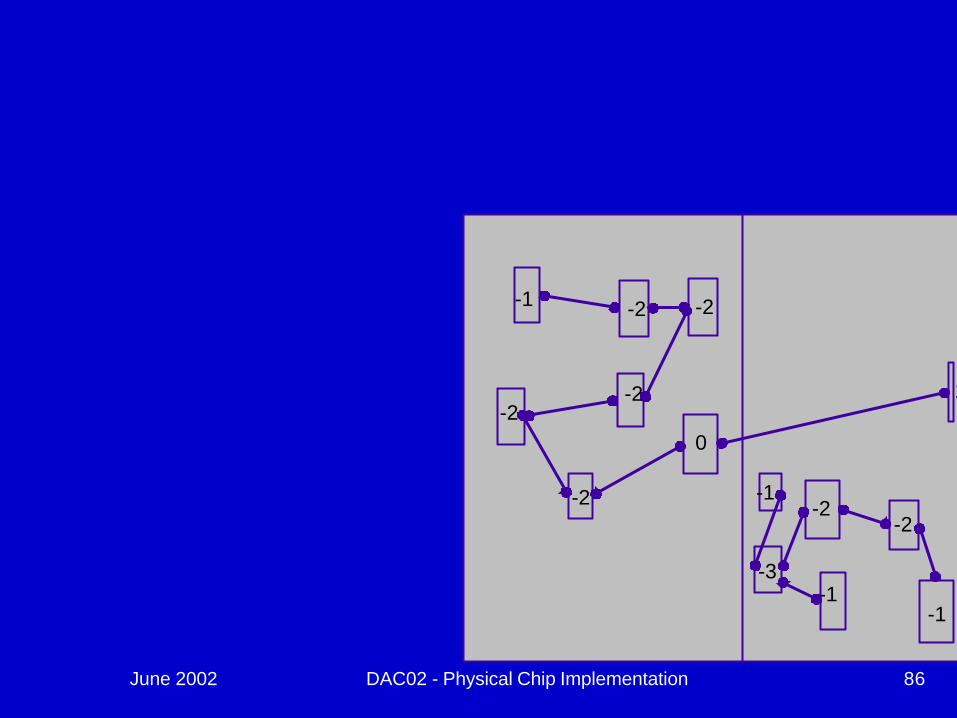
June 2002 DAC02 - Physical Chip Implementation 86
-1
-2
-1
-3
-2
-2
-2
0
-2
-1
1
-1
-2
-2
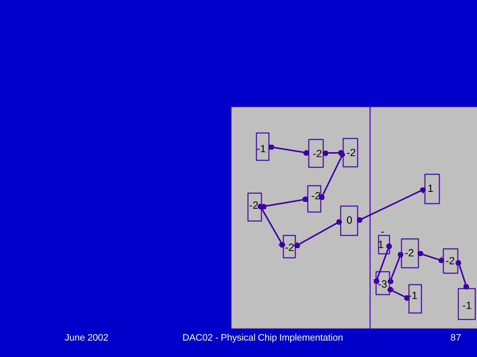
June 2002 DAC02 - Physical Chip Implementation 87
-1
-2
-1
-3
-2
-2
-2
0
-2
-1
1
-1
-2
-2
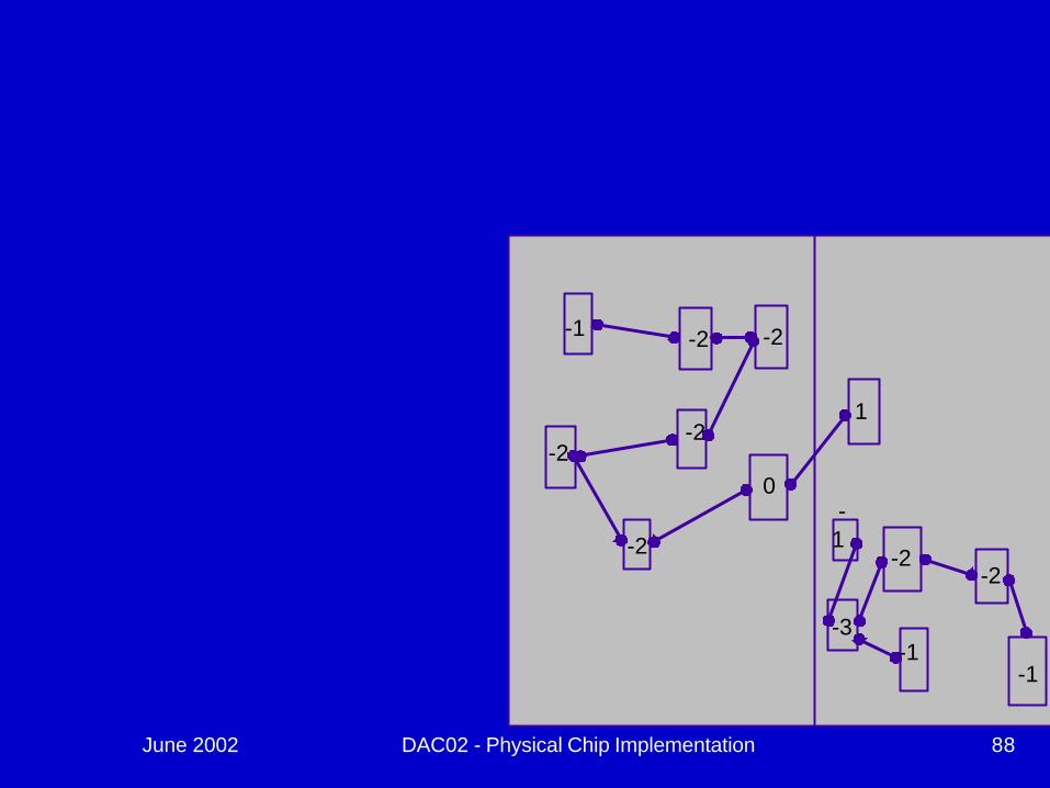
June 2002 DAC02 - Physical Chip Implementation 88
-1
-2
-1
-3
-2
-2
-2
0
-2
-1
1
-1
-2
-2

June 2002 DAC02 - Physical Chip Implementation 89
-1
-2
-1
-3
-2
-2
-2
-2
-2
-1
-1
-1
-2
-2
June 2002 DAC02 - Physical Chip Implementation 90
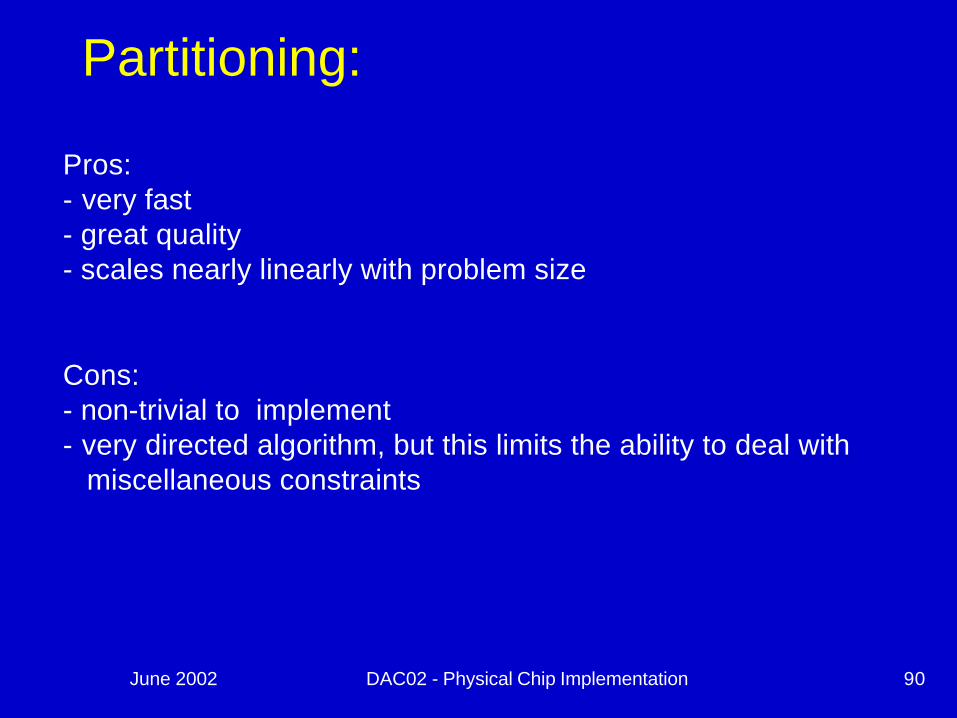
Partitioning:
Pros:- very fast- great quality- scales nearly linearly with problem size
Cons:- non-trivial to implement- very directed algorithm, but this limits the ability to deal with
miscellaneous constraints
June 2002 DAC02 - Physical Chip Implementation 91
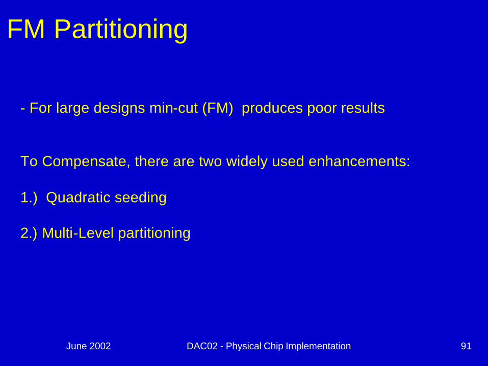
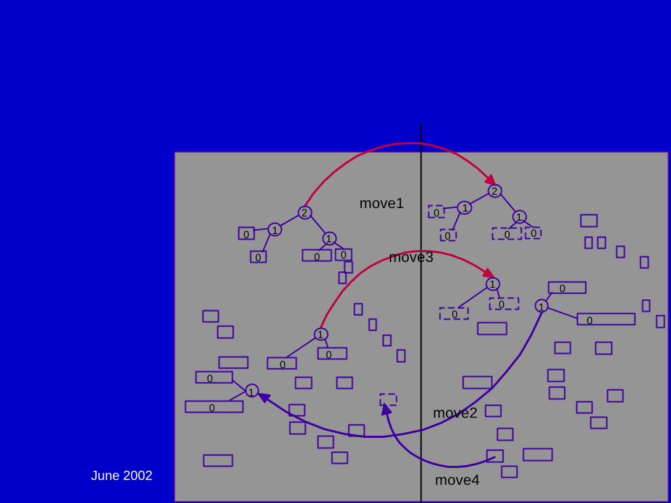
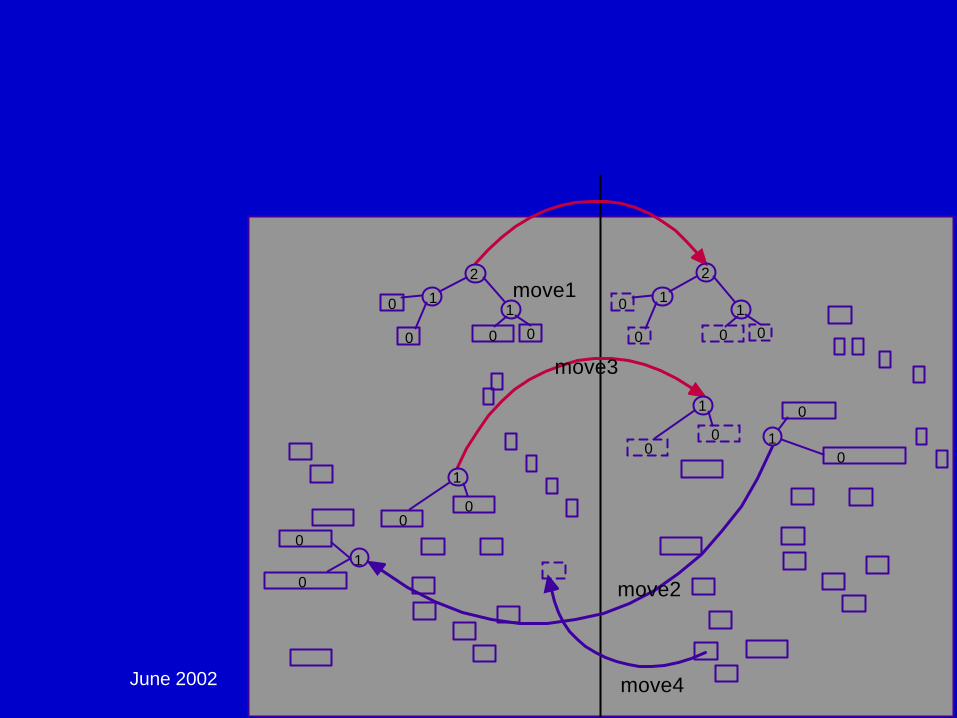
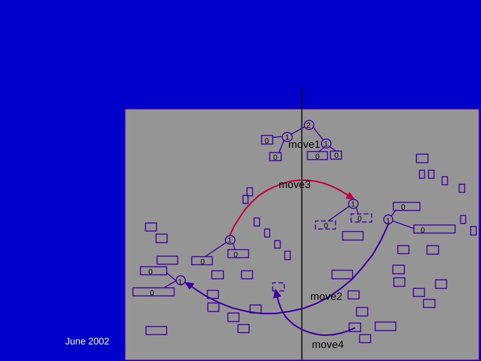
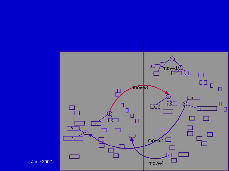
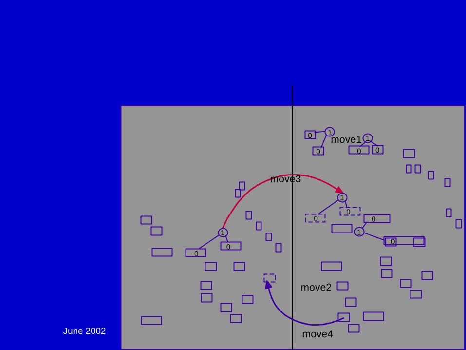
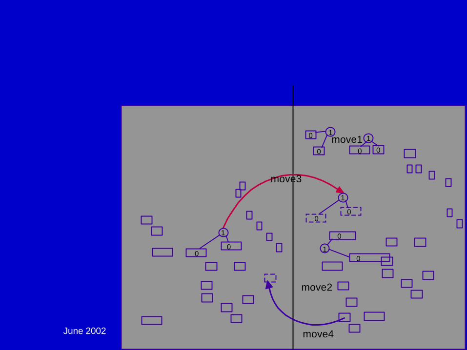
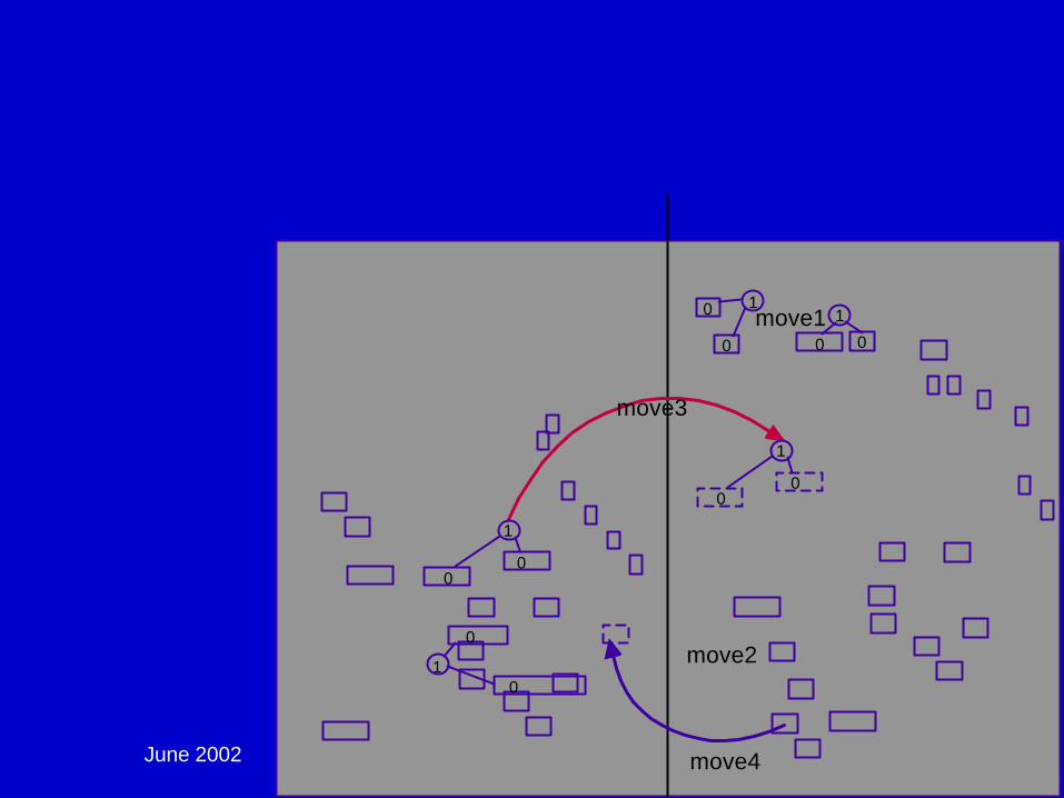
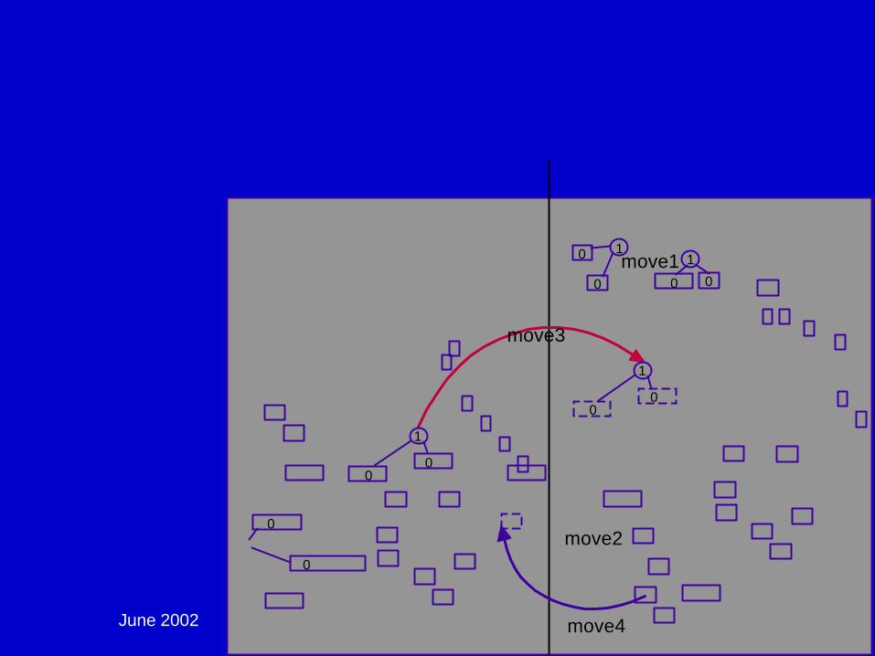
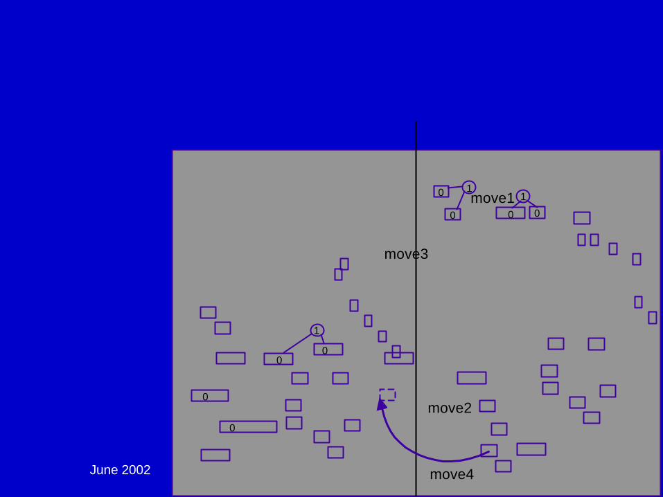
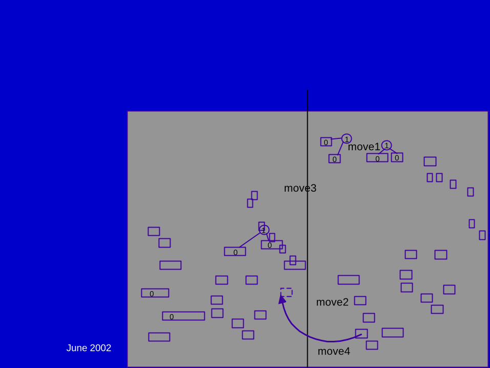
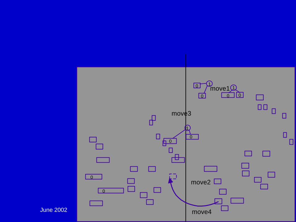
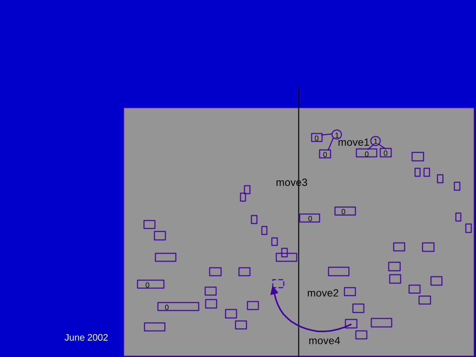
FM Partitioning
- For large designs min-cut (FM) produces poor results
To Compensate, there are two widely used enhancements:
1.) Quadratic seeding
2.) Multi-Level partitioning

June 2002 DAC02 - Physical Chip Implementation 92
cut linecut line
move1
move2
move4
move3
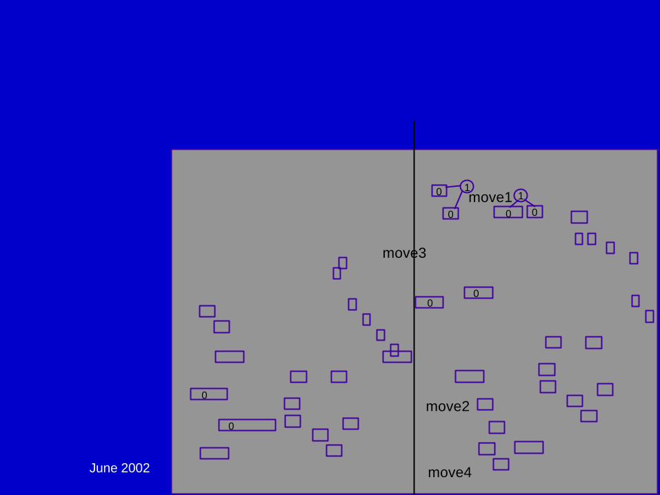
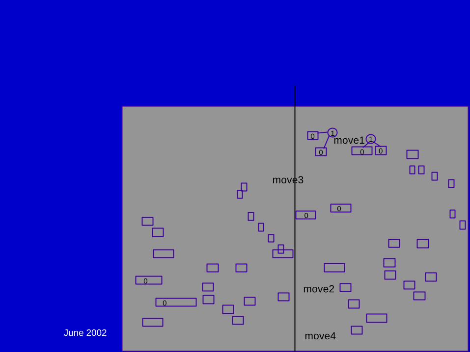
Partitioning:
June 2002 DAC02 - Physical Chip Implementation 93
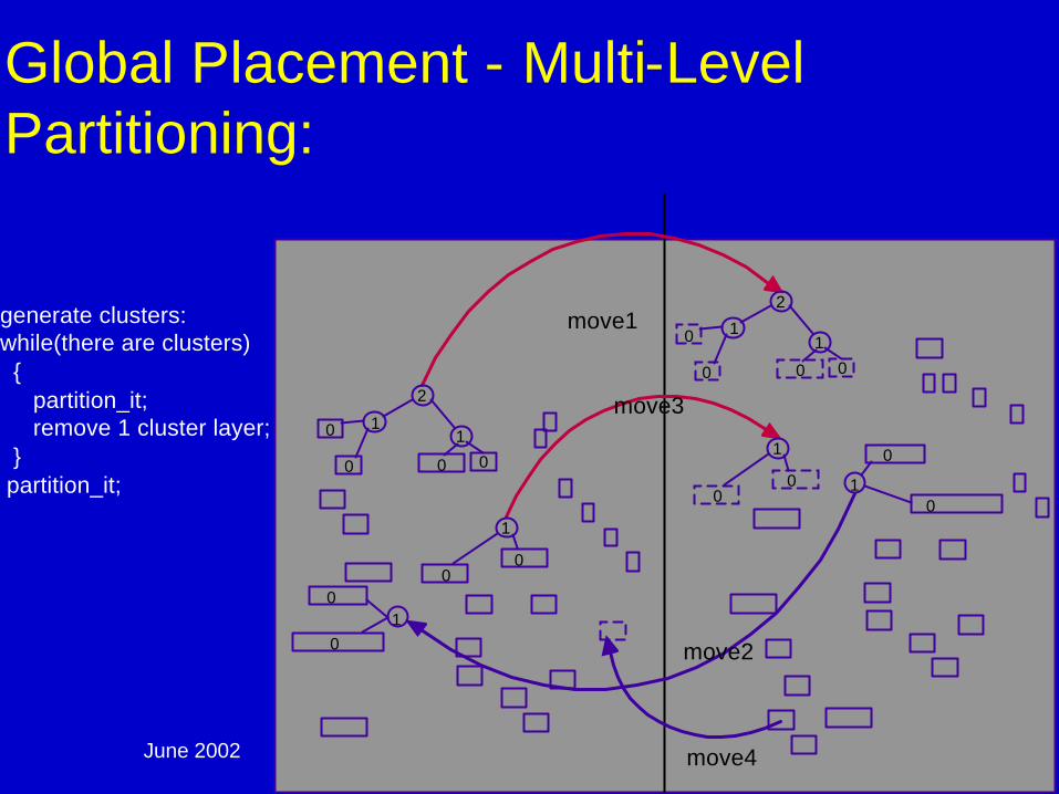
Global Placement - Multi-Level Partitioning:
move1
move2
move4
move3
0 0 0
0 11
2
00
1
1
0 0
0 11
2
0
00
1 0
0
10
0
generate clusters:while(there are clusters)
{partition_it;remove 1 cluster layer;
}partition_it;
June 2002 DAC02 - Physical Chip Implementation 94
move1
move2
move4
move30 0 0
0 11
2
00
1
1
0 0
0 11
2
0
00
1 0
0
10
0
June 2002 DAC02 - Physical Chip Implementation 95
move1
move2
move4
move30 0 0
0 11
2
00
1
1
0 0
0 11
2
0
00
1 0
0
10
0
June 2002 DAC02 - Physical Chip Implementation 96
move1
move2
move4
move30 0 0
0 11
2
00
1
1
0 0
0 11
2
0
00
1 0
0
10
0

June 2002 DAC02 - Physical Chip Implementation 97
move1
move2
move4
move3
0 0 0
0 11
2
00
1
10
0
1 0
0
10
0
June 2002 DAC02 - Physical Chip Implementation 98
move1
move2
move4
move3
0 0 0
0 11
2
00
1
10
0
1 0
0
10
0
June 2002 DAC02 - Physical Chip Implementation 99
move1
move2
move4
move3
0 0 0
0 11
2
00
1
10
0
1 0
0
10
0

June 2002 DAC02 - Physical Chip Implementation 100
move1
move2
move4
move3
0 0 0
0 11
00
1
10
0
1 0
0
10
0

June 2002 DAC02 - Physical Chip Implementation 101
move1
move2
move4
move3
0 0 0
0 11
00
1
10
0
1 0
0
10
0
June 2002 DAC02 - Physical Chip Implementation 102
move1
move2
move4
move3
0 0 0
0 11
00
1 1
00
1
0
0
June 2002 DAC02 - Physical Chip Implementation 103
move1
move2
move4
move3
0 0 0
0 11
00
1
1
00
1
0
0

June 2002 DAC02 - Physical Chip Implementation 104
move1
move2
move4
move3
0 0 0
0 11
00
1
1
00
1
0
0
June 2002 DAC02 - Physical Chip Implementation 105
move1
move2
move4
move3
0 0 0
0 11
00
1
1
00
1
0
0

June 2002 DAC02 - Physical Chip Implementation 106
move1
move2
move4
move3
0 0 0
0 11
00
1
1
00
1
0
0
June 2002 DAC02 - Physical Chip Implementation 107
move1
move2
move4
move3
0 0 0
0 11
00
1
00
1
0
0

June 2002 DAC02 - Physical Chip Implementation 108
move1
move2
move4
move3
0 0 0
0 11
00
1
00
1
0
0
June 2002 DAC02 - Physical Chip Implementation 109
move1
move2
move4
move3
0 0 0
0 11
00
1
0
0
June 2002 DAC02 - Physical Chip Implementation 110
move1
move2
move4
move3
0 0 0
0 11
00
1
0
0
June 2002 DAC02 - Physical Chip Implementation 111
move1
move2
move4
move3
0 0 0
0 11
00
1
0
0

June 2002 DAC02 - Physical Chip Implementation 112
move1
move2
move4
move3
0 0 0
0 11
00
1
0
0

June 2002 DAC02 - Physical Chip Implementation 113
move1
move2
move4
move3
0 0 0
0 11
00
0
0
June 2002 DAC02 - Physical Chip Implementation 114
move1
move2
move4
move3
0 0 0
0 11
00
0
0
June 2002 DAC02 - Physical Chip Implementation 115
move1
move2
move4
move3
0 0 0
0 11
00
0
0

June 2002 DAC02 - Physical Chip Implementation 116
move1
move2
move4
move3
0 0 0
0 11
00
0
0

June 2002 DAC02 - Physical Chip Implementation 117
move1
move2
move4
move3
0 0 0
0 11
00
0
0
June 2002 DAC02 - Physical Chip Implementation 118
move1
move2
move4
move3
0 0 0
0 11
00
0
0

June 2002 DAC02 - Physical Chip Implementation 119
MLP/FM Partitioning Cons:
n Does not know how to handle “free” spacen Results tend to be erratic, ie results from run
to run have significant variation

June 2002 DAC02 - Physical Chip Implementation 120
MLP/FM Partitioning Pros:
n Handles designs that have no fixed connection points
n Very fast - can handle large designs

June 2002 DAC02 - Physical Chip Implementation 121
Hybrid Techniques
n Use both MLP and Quadratic techniques
n Results are more predictable due to quadratic cost function
n Partitioning is used for overlap removaln Quadratic is used for “free” space
handling and some relative order indications
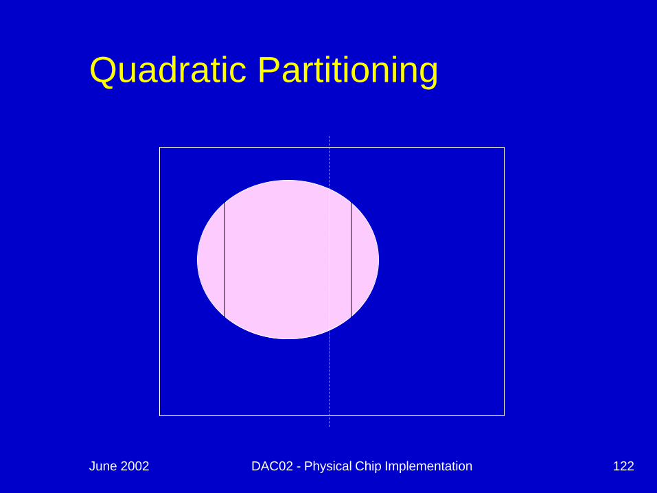
June 2002 DAC02 - Physical Chip Implementation 122
Quadratic Partitioning
June 2002 DAC02 - Physical Chip Implementation 123
June 2002 DAC02 - Physical Chip Implementation 124

June 2002 DAC02 - Physical Chip Implementation 125

June 2002 DAC02 - Physical Chip Implementation 126

June 2002 DAC02 - Physical Chip Implementation 127
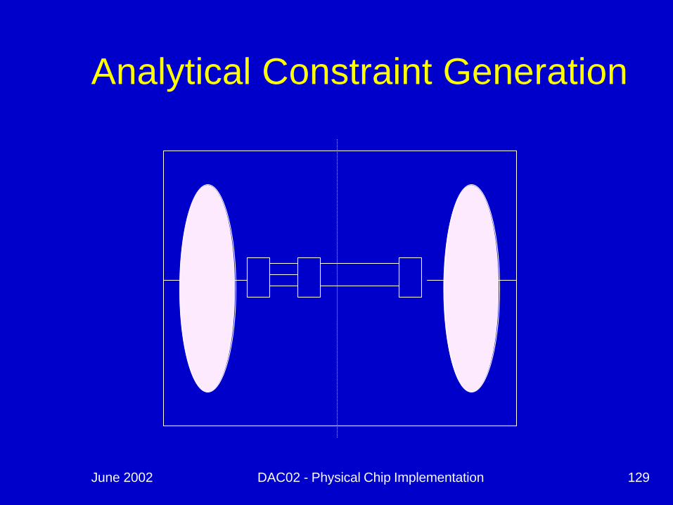
Analytical Constraint Generation
n Combine Quadratic techniques with MLP
n Use Quadratic solution to determine global position (ie balance)
n Use MLP to determine relative ordering of cells

June 2002 DAC02 - Physical Chip Implementation 128
Poor Solution
Analytical Constraint Generation
Capacity = 2 Capacity = 2
Quadratic solution Area=1Analytical constraintACG solution
June 2002 DAC02 - Physical Chip Implementation 129
Analytical Constraint Generation

June 2002 DAC02 - Physical Chip Implementation 130

June 2002 DAC02 - Physical Chip Implementation 131
June 2002 DAC02 - Physical Chip Implementation 132
June 2002 DAC02 - Physical Chip Implementation 133

June 2002 DAC02 - Physical Chip Implementation 134
June 2002 DAC02 - Physical Chip Implementation 135

June 2002 DAC02 - Physical Chip Implementation 136

June 2002 DAC02 - Physical Chip Implementation 137
June 2002 DAC02 - Physical Chip Implementation 138

June 2002 DAC02 - Physical Chip Implementation 139

June 2002 DAC02 - Physical Chip Implementation 140

June 2002 DAC02 - Physical Chip Implementation 141
June 2002 DAC02 - Physical Chip Implementation 142
June 2002 DAC02 - Physical Chip Implementation 143

June 2002 DAC02 - Physical Chip Implementation 144
June 2002 DAC02 - Physical Chip Implementation 145

June 2002 DAC02 - Physical Chip Implementation 146

June 2002 DAC02 - Physical Chip Implementation 147

June 2002 DAC02 - Physical Chip Implementation 148
June 2002 DAC02 - Physical Chip Implementation 149
June 2002 DAC02 - Physical Chip Implementation 150
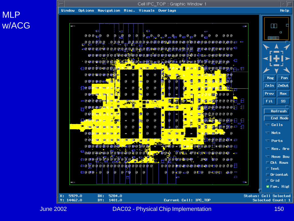
MLPw/ACG

June 2002 DAC02 - Physical Chip Implementation 151
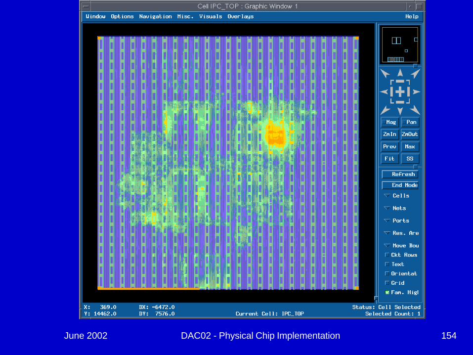
Global Route Results::
June 2002 DAC02 - Physical Chip Implementation 152
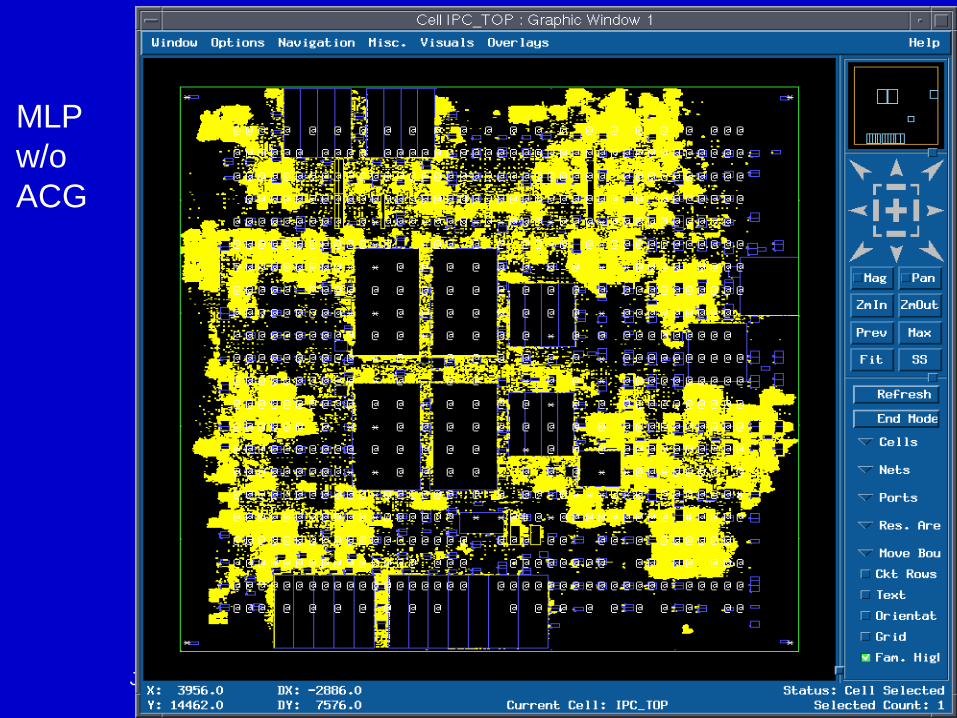
MLPw/o ACG
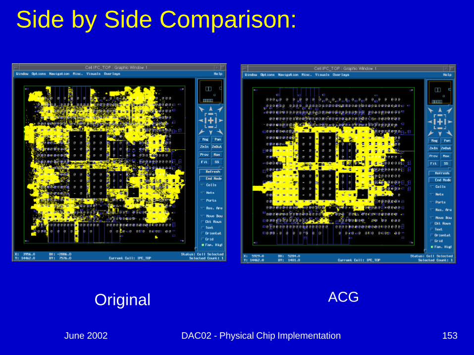
June 2002 DAC02 - Physical Chip Implementation 153
Original ACG
Side by Side Comparison:
June 2002 DAC02 - Physical Chip Implementation 154

June 2002 DAC02 - Physical Chip Implementation 155
June 2002 DAC02 - Physical Chip Implementation 156
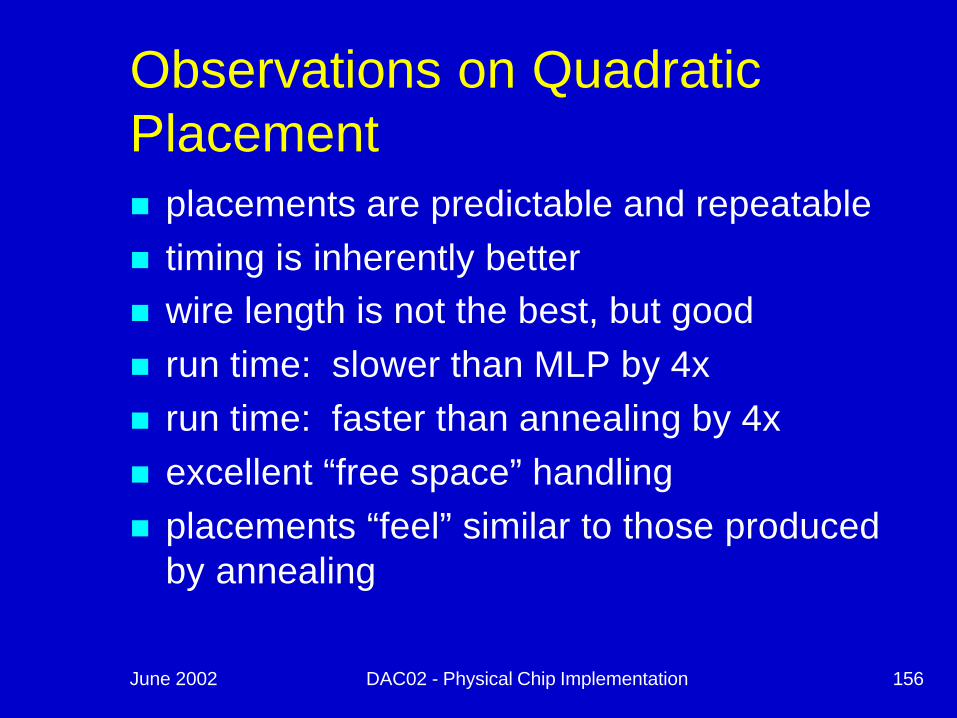
Observations on Quadratic Placementn placements are predictable and repeatablen timing is inherently bettern wire length is not the best, but goodn run time: slower than MLP by 4xn run time: faster than annealing by 4xn excellent “free space” handlingn placements “feel” similar to those produced
by annealing
June 2002 DAC02 - Physical Chip Implementation 157
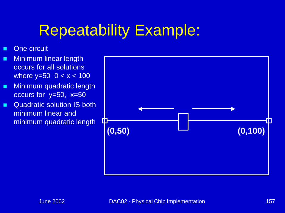
Repeatability Example:n One circuitn Minimum linear length
occurs for all solutions where y=50 0 < x < 100
n Minimum quadratic length occurs for y=50, x=50
n Quadratic solution IS both minimum linear and minimum quadratic length
(0,50) (0,100)
June 2002 DAC02 - Physical Chip Implementation 158
Section Outlinen Introductionn Review material (timing and synthesis)n Introduction to placementn Placement algorithmsn Paradigms for placement-synthesis
integrationn Placement aware synthesis techniquesn Congestion avoidance / mitigation techniquesn Routing optimization

June 2002 DAC02 - Physical Chip Implementation 159
Synthesis - Placement Interface

June 2002 DAC02 - Physical Chip Implementation 160
Read Data
Divide each Partition
Preprocessing
Detailed Placement
While ( any partition has > 2 cells )
Reflow across partitions
Done
Partitioning Algorithm: Partition & Reflow
Global Placement
Netlist
SynthesisSynthesis
June 2002 DAC02 - Physical Chip Implementation 161
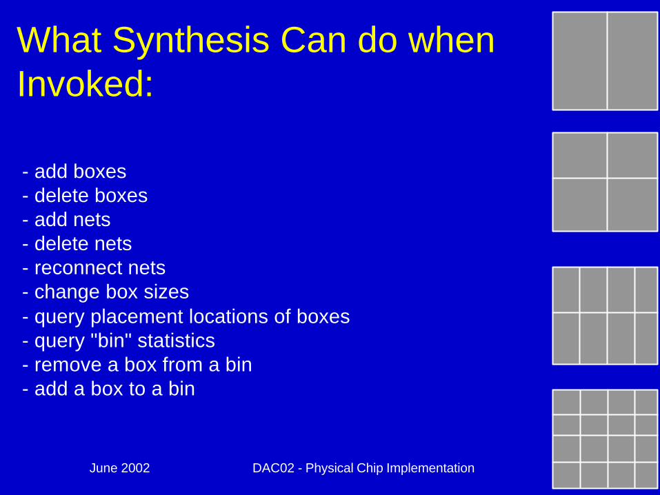
What Synthesis Can do when Invoked:
- add boxes- delete boxes- add nets- delete nets- reconnect nets- change box sizes- query placement locations of boxes- query "bin" statistics- remove a box from a bin- add a box to a bin
June 2002 DAC02 - Physical Chip Implementation 162
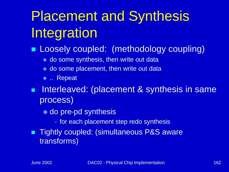
Placement and Synthesis Integrationn Loosely coupled: (methodology coupling)
u do some synthesis, then write out datau do some placement, then write out datau .. Repeat
nn Interleaved: (placement & synthesis in same process)u do pre-pd synthesis
F for each placement step redo synthesis
n Tightly coupled: (simultaneous P&S aware transforms)

June 2002 DAC02 - Physical Chip Implementation 163
Loosely Coupled Placement & Synthesis:
Characteristics:
- Placement is treated as a black box
- Multiple placement runs are made
Do Placement
Analyze
- re-synthesize- GenerateConstraints
Meet Objectives
Done w/placement
Yes
No

June 2002 DAC02 - Physical Chip Implementation 164
SynthesisSynthesis
Synthesis
Synthesis
Interleaved Placement & Synthesis:
Characteristics:
- the placement flow is the same as ina placement only methodology
- in between each step of the placementprogression, synthesis is invoked
June 2002 DAC02 - Physical Chip Implementation 165
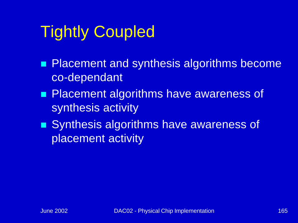
Tightly Coupled
n Placement and synthesis algorithms become co-dependant
n Placement algorithms have awareness of synthesis activity
n Synthesis algorithms have awareness of placement activity
June 2002 DAC02 - Physical Chip Implementation 166
Section Outlinen Introductionn Review material (timing and synthesis)n Introduction to placementn Placement algorithmsn Paradigms for placement-synthesis
integrationn Placement aware synthesis techniquesn Congestion avoidance / mitigation techniquesn Routing optimization
June 2002 DAC02 - Physical Chip Implementation 167
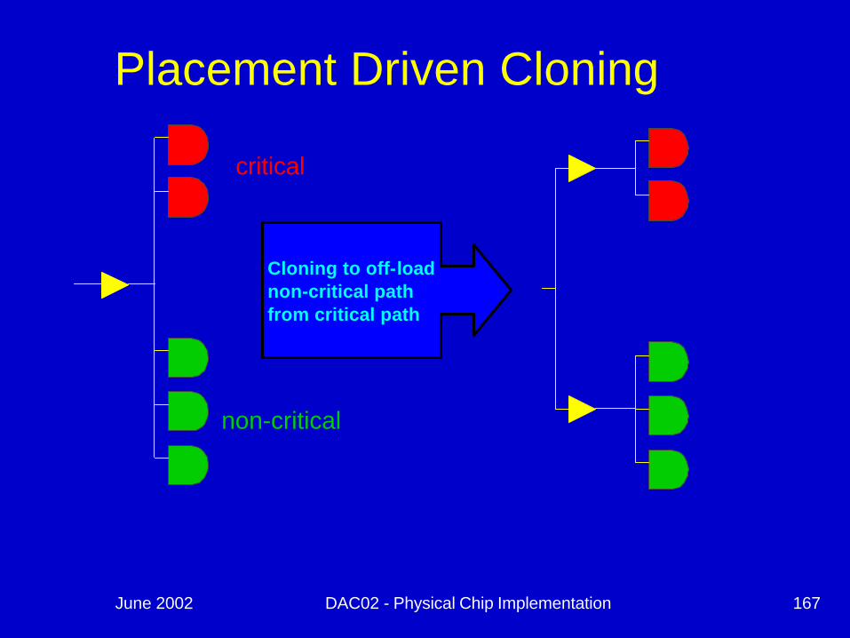
Placement Driven Cloning
critical
non-critical
Cloning to off-load non-critical path from critical path
June 2002 DAC02 - Physical Chip Implementation 168
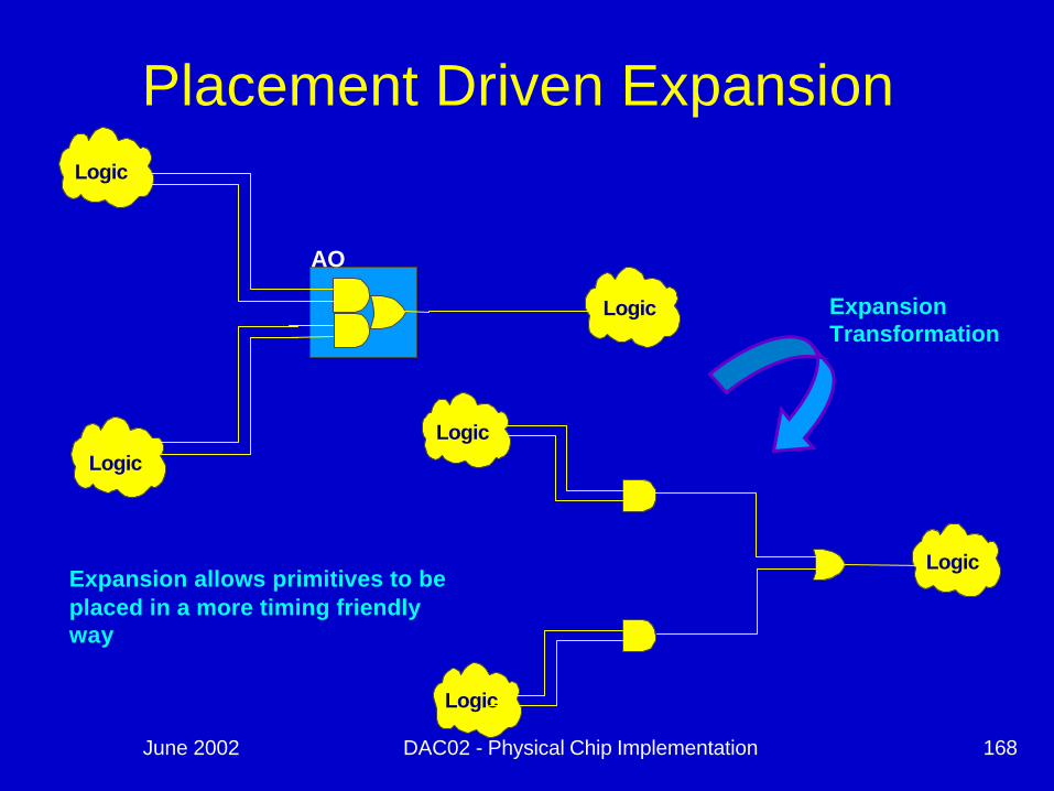
Placement Driven ExpansionLogic
Logic
AO
LogicLogic
Logic
LogicExpansion allows primitives to be placed in a more timing friendly way
Expansion Transformation
June 2002 DAC02 - Physical Chip Implementation 169
Example:
Tightly Coupled Placement Driven Expansion
June 2002 DAC02 - Physical Chip Implementation 170
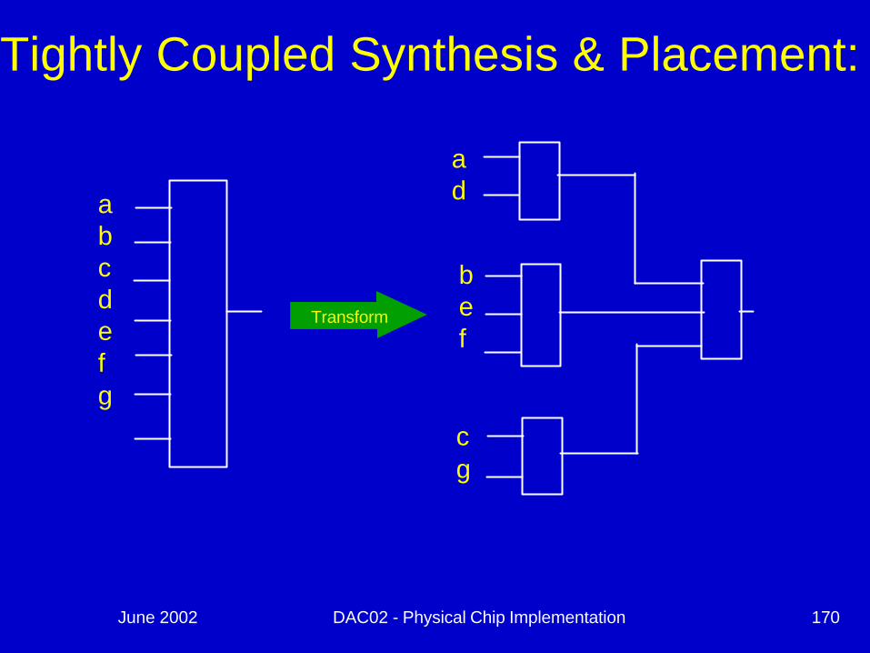
Tightly Coupled Synthesis & Placement:
abcdefg
Transform
ad
bef
cg

June 2002 DAC02 - Physical Chip Implementation 171
ab
c
d e
fg
Tightly Coupled Synthesis & Placement Example:
Suppose the primary IO constraints look like this:

June 2002 DAC02 - Physical Chip Implementation 172
Tightly Coupled Synthesis & Placement Example:
ab
c
d e
fg
The placement of the synthesized netlist would look something like this:
June 2002 DAC02 - Physical Chip Implementation 173
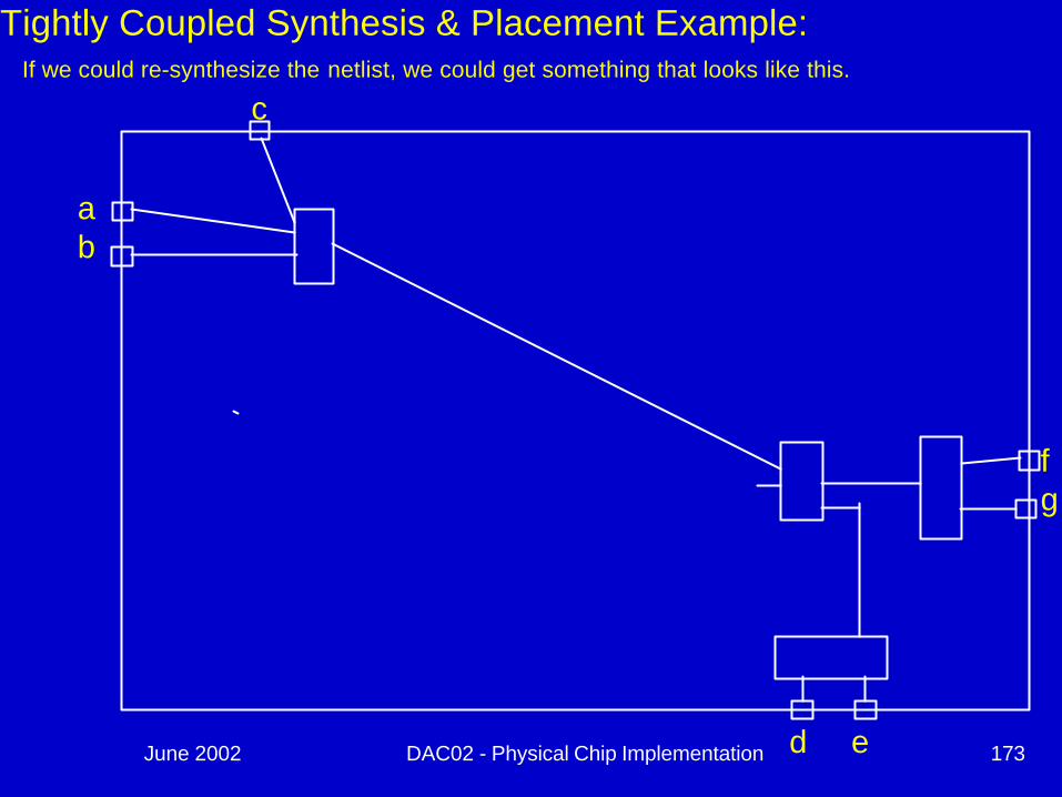
Tightly Coupled Synthesis & Placement Example:
ab
c
d e
fg
If we could re-synthesize the netlist, we could get something that looks like this.

June 2002 DAC02 - Physical Chip Implementation 174
Tightly Coupled Synthesis & Placement:
abc
defg
PD-MAP
abc
defg
weight = 1/10
weight = 1
June 2002 DAC02 - Physical Chip Implementation 175
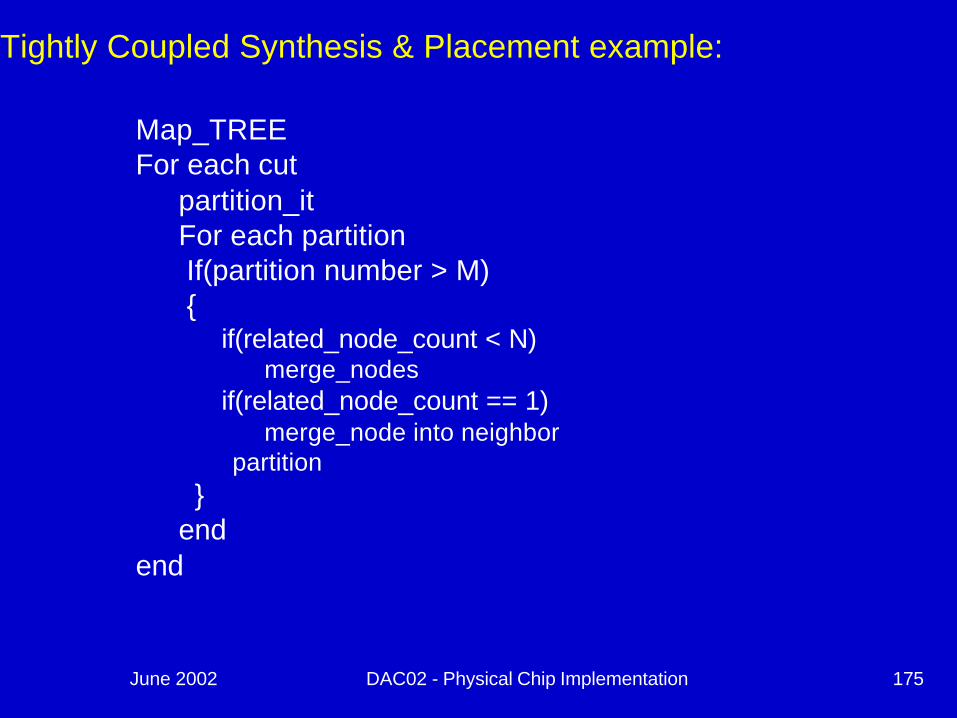
Tightly Coupled Synthesis & Placement example:
Map_TREEFor each cut
partition_itFor each partitionIf(partition number > M){
if(related_node_count < N)merge_nodes
if(related_node_count == 1)merge_node into neighbor
partition}
endend
June 2002 DAC02 - Physical Chip Implementation 176
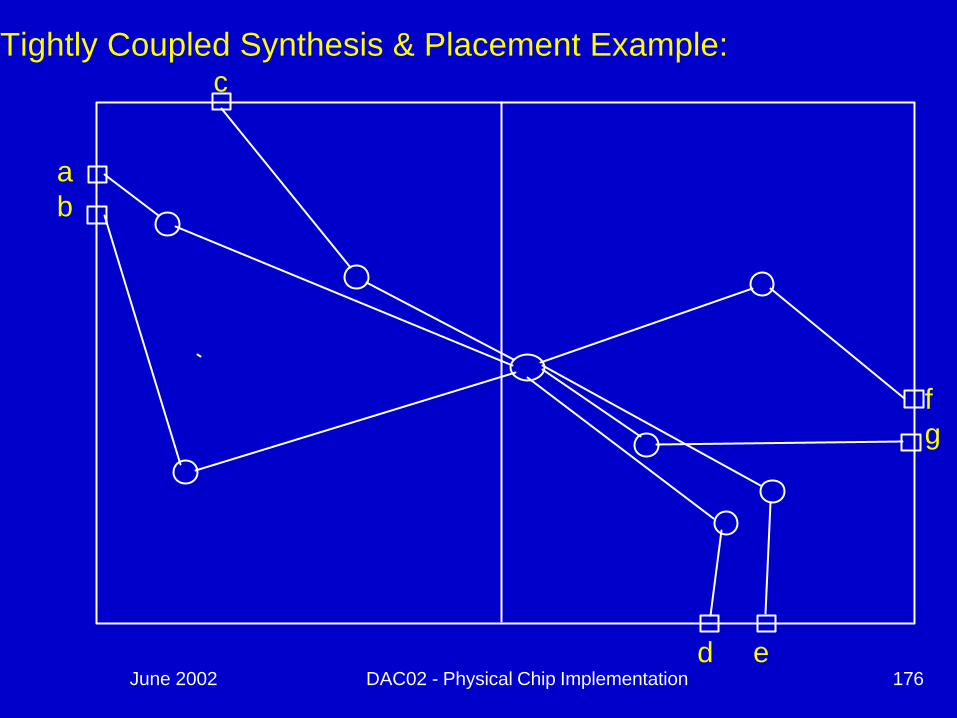
Tightly Coupled Synthesis & Placement Example:
ab
c
d e
fg
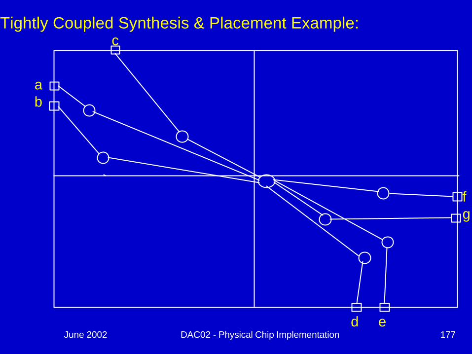
June 2002 DAC02 - Physical Chip Implementation 177
Tightly Coupled Synthesis & Placement Example:
ab
c
d e
fg

June 2002 DAC02 - Physical Chip Implementation 178
Tightly Coupled Synthesis & Placement Example:
ab
c
d e
fg

June 2002 DAC02 - Physical Chip Implementation 179
Tightly Coupled Synthesis & Placement Example:
ab
c
d e
fg
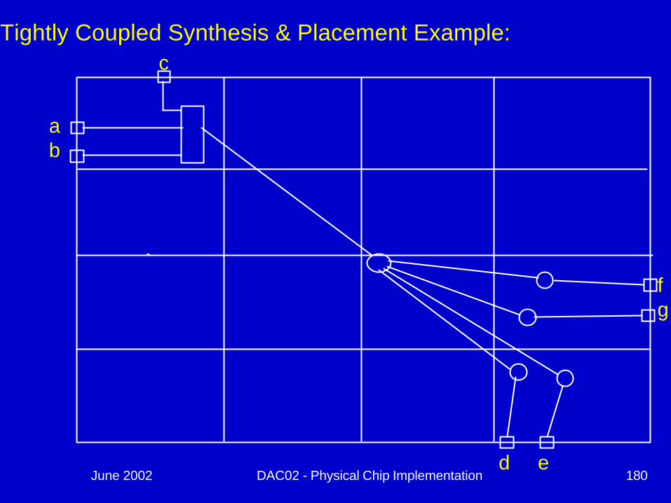
June 2002 DAC02 - Physical Chip Implementation 180
Tightly Coupled Synthesis & Placement Example:
ab
c
d e
fg
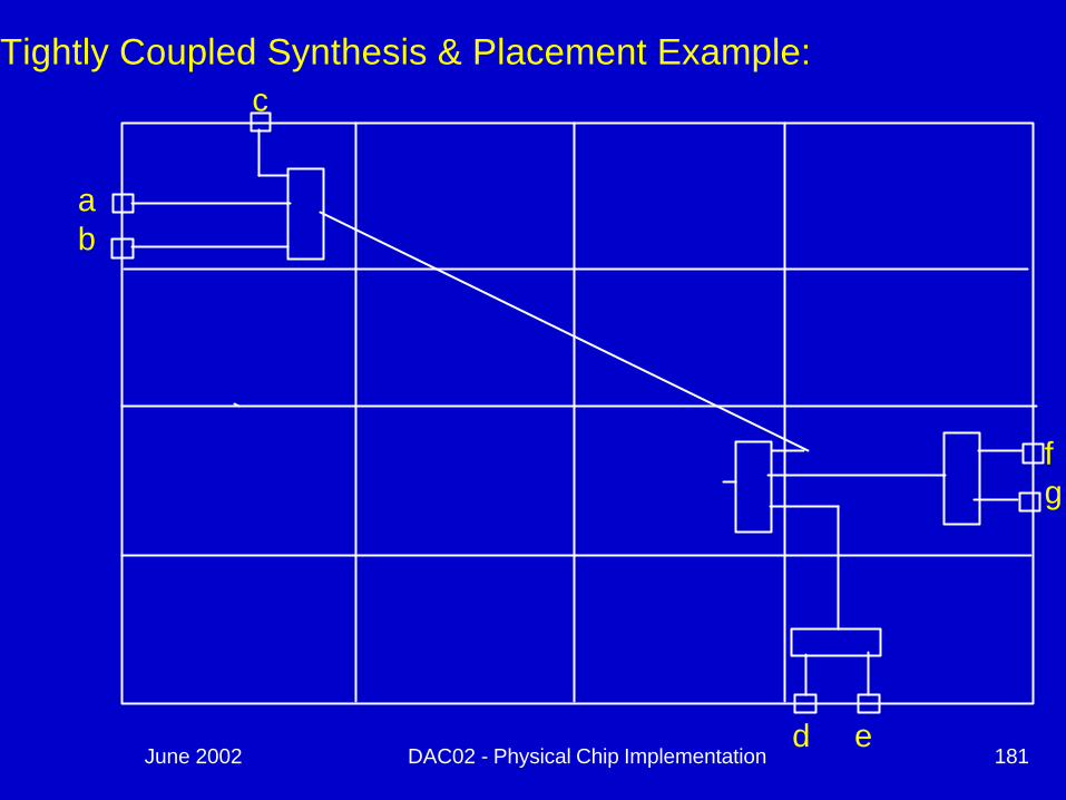
June 2002 DAC02 - Physical Chip Implementation 181
Tightly Coupled Synthesis & Placement Example:
ab
c
d e
fg
June 2002 DAC02 - Physical Chip Implementation 182
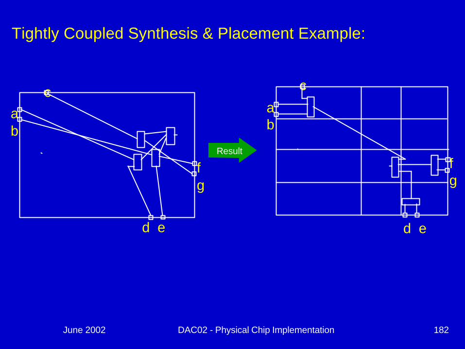
Tightly Coupled Synthesis & Placement Example:
ab
c
d e
fg
ab
c
fg
d e
Result

June 2002 DAC02 - Physical Chip Implementation 183
Placement Driven Timing Correction

June 2002 DAC02 - Physical Chip Implementation 184
Redesign Fan-in Treea
c
d
b eArr(b)=3
Arr(c)=1
Arr(d)=0
Arr(a)=4
Arr(e)=6
1
1
1
c
d
e
Arr(e)=5
1
1b1
a
e
e
Arr(e)=0

June 2002 DAC02 - Physical Chip Implementation 185
Placement Driven Repowering
n Repowering is traditionally done using load based cell characterization
n Placement changes continuously during partitioning
n Need high efficiency algorithms to do repowering in this environment
n Solution: Use Gain Based Formulation
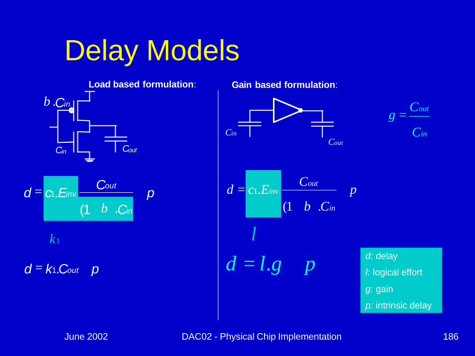
June 2002 DAC02 - Physical Chip Implementation 186
Delay Models
inC in
out
C
Cg =
outC
pC
CEcdin
outinv +
).+=
β1(. .1
pCkd out += .1
Load based formulation:
pgld += .
inC.β
inC outC
Gain based formulation:
pC
CEcdin
outinv +
).+=
β1(. .1
d: delay
l: logical effort
g: gain
p: intrinsic delay
1k l

June 2002 DAC02 - Physical Chip Implementation 187
Area vs Delay Centricn Load Based Paradigm
• (load-based delay eq.)
• sizedn Know:
u Size of each cellu Total Area ->
– area centricn Don’t know:
u Wire loadsu Delay of each cellu Delay of a path
n Estimation error is in the delay:u Local ‘path based’ property.
n Gain Based Paradigm• (gain based delay
eq.)• sizeless
n Know:u The delay of each cell.u The delay of a path ->
– delay centricn Don’t know:
u Wire loadsu The area of each cellu The total area
n Estimation error is in the areau Global property.
June 2002 DAC02 - Physical Chip Implementation 188
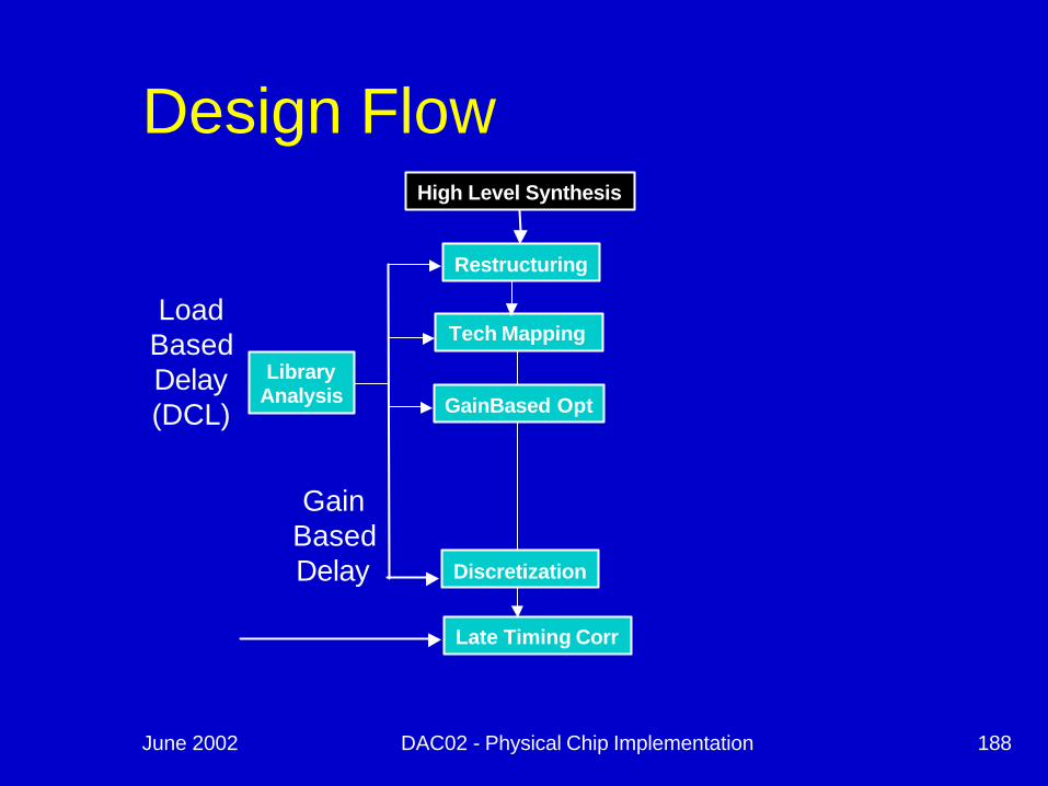
Design FlowHigh Level Synthesis
Restructuring
Tech Mapping
Late Timing Corr
LibraryAnalysis GainBased Opt
Discretization
LoadBasedDelay(DCL)
GainBasedDelay
June 2002 DAC02 - Physical Chip Implementation 189
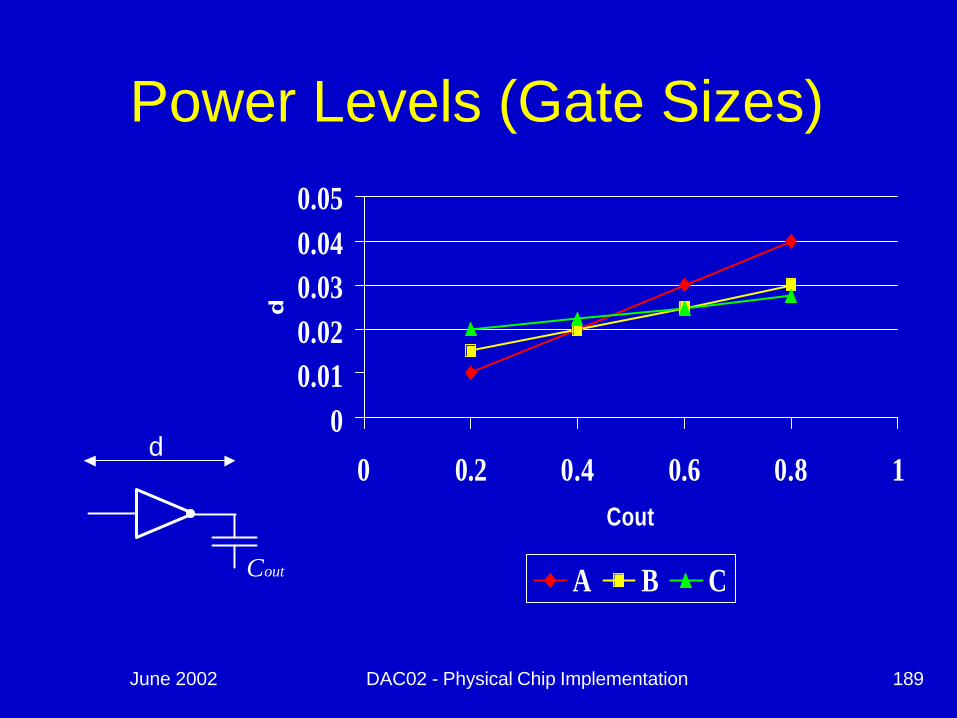
Power Levels (Gate Sizes)
00.010.020.030.040.05
0 0.2 0.4 0.6 0.8 1Cout
d
A B CoutC
d
June 2002 DAC02 - Physical Chip Implementation 190
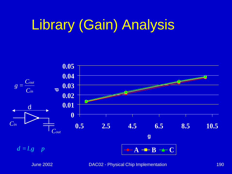
Library (Gain) Analysis
00.010.020.030.040.05
0.5 2.5 4.5 6.5 8.5 10.5g
d
A B C
in
out
CCg =
pgld += .
inCoutC
d
June 2002 DAC02 - Physical Chip Implementation 191
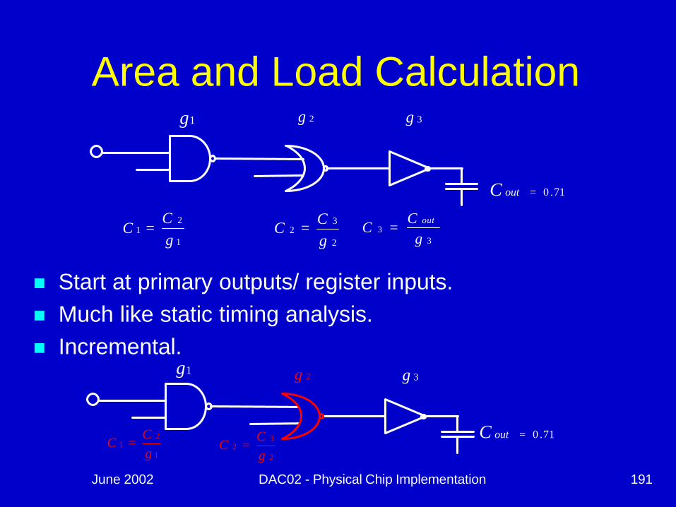
Area and Load Calculation
n Start at primary outputs/ register inputs. n Much like static timing analysis.n Incremental.
1g 2g 3g
33
gC
Cout
=2
32
gCC =
1
21
gC
C =
71.0=outC
71.0=outC
1g 2g 3g
2
32
gC
C =1
21
gC
C =

June 2002 DAC02 - Physical Chip Implementation 192
Gain Calculation
outCinC
1d 3dD
4d2d
43211
dddddDN
ii +++== ∑
=
in
outout
in
N
ii C
CCC
CC
CC
CCgggggG ==
=== ∏
43
4
2
3.
24321
1....
Minimize D such that:in
out
CCG =
∑∑==
+=N
ii
N
ii pfD
11 CinCout
LN
igi
N
ili
N
ifiF .
1.
11=∏
=∏=
=∏=
=
Solution: ffi =Geometric
pfpgld +=+= .
Minimize Such that:

June 2002 DAC02 - Physical Chip Implementation 193
Example I
71.0=outC19.0=inC
1d
2
3021.00496.0 :NOR2CC
d ×+=
inCC
d2
011.00308.0 :NAND2 ×+=
3009.00295.0 :INV
CC
d out×+=
2d 3d
000008.03
3.21. ====in
out
CCLffffF
0203.0=f
Nand2 Nor2 Inv Path
p 0.0308 0.0496 0.0295 0.1099
f 0.0203 0.0203 0.0203 0.0609
d 0.0511 0.0699 0.0498 0.1708
Cin 0.19 0.3364 0.3283 .
3C2C
June 2002 DAC02 - Physical Chip Implementation 194
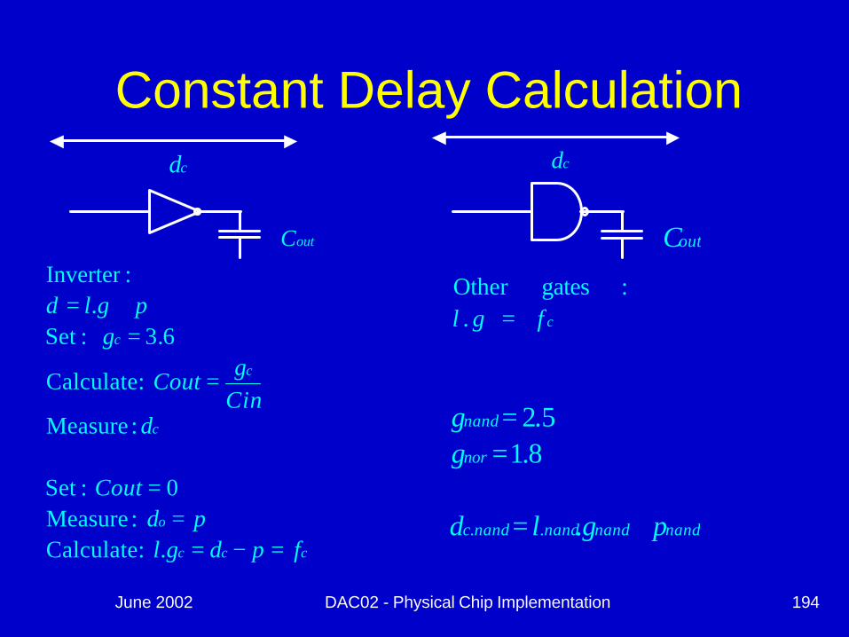
Constant Delay Calculation
outC
ccc
o
c
c
c
fpdglpd
Cout
dCingCout
gpgld
=−==
=
=
=+=
. :Calculate :Measure
0 :Set
:Measure
:Calculate
6.3 :Set.
:Inverter
cd
nandnandnandnandc
nor
nand
pgld
gg
+=
==
.
8.15.2
..
outC
cd
cfgl =.:gatesOther

June 2002 DAC02 - Physical Chip Implementation 195
Discretizationn From gain-based model back to appropriate power levelsn There is an error in timing/load when ‘ideal’ power levels are not
available.u Goal: Minimize this error.u Can be tuned to delay error or capacitance error..
1g 2g 3g
33
gC
Cout
=2
32
gCC =
1
21
gC
C =
71.0=outC
pgld += .
[Kudva98][Beeftink98]

June 2002 DAC02 - Physical Chip Implementation 196
Gain Based: Observations:n Gain Based algorithms: A major improvement.
u More homogeneous (global) algorithms and designs.u Can be better targeted for area and/or delay.
n Reveal inherent cell characteristics to optimization tools, leading to improved QOR
n Good library design is required to facilitate discretization step
n Ideally suited for operation within Physical Synthesis

June 2002 DAC02 - Physical Chip Implementation 197
Placement Driven Buffering
Rip Out all Buffers
Insert Buffers based on placement info

June 2002 DAC02 - Physical Chip Implementation 198
What to do About Long Wires?
n Add buffersn Tune wire sizesn Modify the placement to reduce them
June 2002 DAC02 - Physical Chip Implementation 199
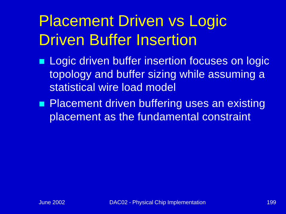
Placement Driven vs Logic Driven Buffer Insertionn Logic driven buffer insertion focuses on logic
topology and buffer sizing while assuming a statistical wire load model
n Placement driven buffering uses an existing placement as the fundamental constraint
June 2002 DAC02 - Physical Chip Implementation 200
n Multiple buffer typesn Invertersn Capacitance, Slew and Noise constraintsn Wire Sizingn Simultaneous driver sizingn High order interconnect delay and Ceffectiven Blockage handling
Placement Driven Buffer Insertion: Buffopt (IBM)
June 2002 DAC02 - Physical Chip Implementation 201
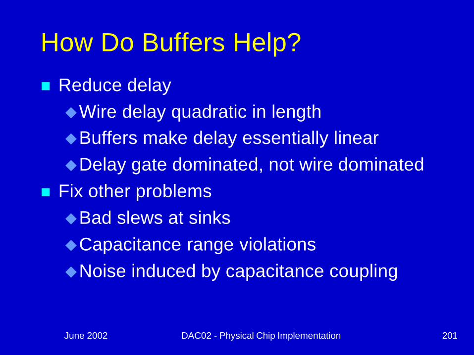
How Do Buffers Help?
n Reduce delayuWire delay quadratic in lengthuBuffers make delay essentially linearuDelay gate dominated, not wire dominated
n Fix other problemsuBad slews at sinksuCapacitance range violationsuNoise induced by capacitance coupling

June 2002 DAC02 - Physical Chip Implementation 202
How Does Wire Sizing Help?
n Highly resistive lines increase delayn Wider wires or thick metal layers reduces
resistance, but can increase capacitancen For long interconnect, resistance reduction
outweighs capacitance increase

June 2002 DAC02 - Physical Chip Implementation 203
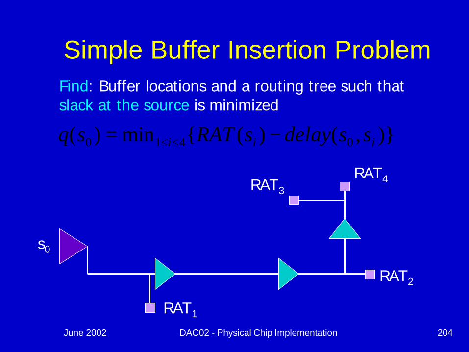
Simple Buffer Insertion ProblemGiven: Source and sink locations, sink capacitancesand RATs, a buffer type, source delay rules, unit wire resistance and capacitance
Buffer
RAT1
RAT2
RAT3
RAT4
s0
June 2002 DAC02 - Physical Chip Implementation 204
Simple Buffer Insertion ProblemFind: Buffer locations and a routing tree such that slack at the source is minimized
RAT2
RAT3
RAT4
RAT1
s0
)},()({min)( 0410 iii ssdelaysRATsq −= ≤≤

June 2002 DAC02 - Physical Chip Implementation 205
Fundamental Buffer Insertion
n Van Ginneken’s dynamic programming algorithm
n Building block: candidate (Cap, slack)uCandidates for each node stored as a listuEach sink has one candidateuPropagate candidates up the tree
n Guarantees optimal solutionn Quadratic complexity
June 2002 DAC02 - Physical Chip Implementation 206
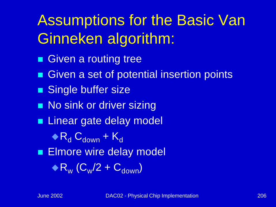
Assumptions for the Basic Van Ginneken algorithm:n Given a routing treen Given a set of potential insertion pointsn Single buffer sizen No sink or driver sizingn Linear gate delay modeluRd Cdown + Kd
n Elmore wire delay modeluRw (Cw/2 + Cdown)
June 2002 DAC02 - Physical Chip Implementation 207
Van Ginneken Extensions
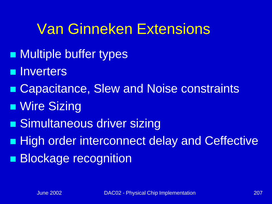
n Multiple buffer typesn Invertersn Capacitance, Slew and Noise constraintsn Wire Sizingn Simultaneous driver sizingn High order interconnect delay and Ceffectiven Blockage recognition
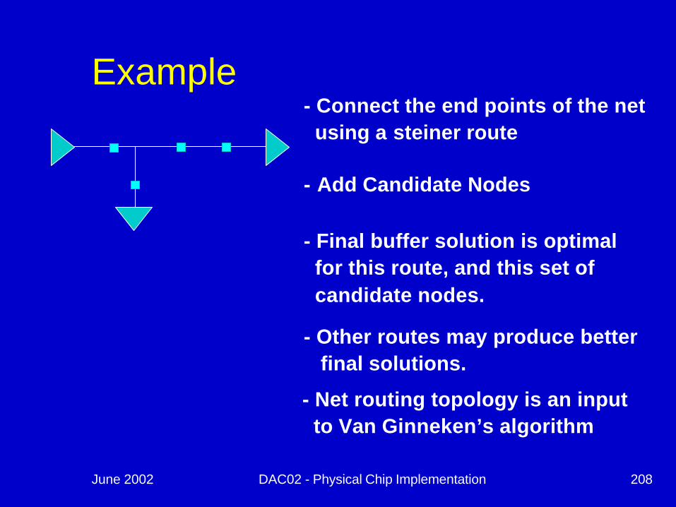
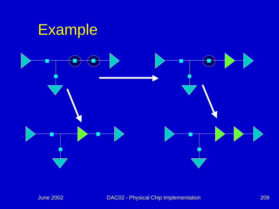
June 2002 DAC02 - Physical Chip Implementation 208
Example- Connect the end points of the netusing a steiner route
- Add Candidate Nodes
- Final buffer solution is optimal for this route, and this set of candidate nodes.
- Other routes may produce betterfinal solutions.
- Net routing topology is an inputto Van Ginneken’s algorithm
June 2002 DAC02 - Physical Chip Implementation 209
Example

June 2002 DAC02 - Physical Chip Implementation 210
How Many Candidates?
n Number of candidates seems to double with each additional node
n Prune candidate with worst slack when capacitances is greater or equal
n Linear number of candidates
June 2002 DAC02 - Physical Chip Implementation 211
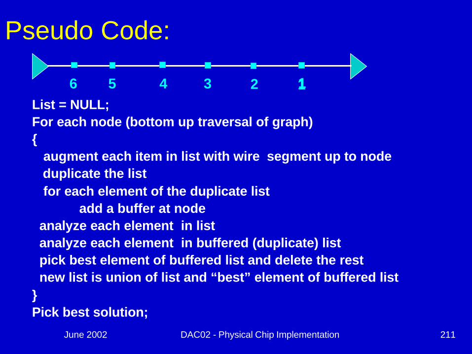
Pseudo Code:
List = NULL;For each node (bottom up traversal of graph){
augment each item in list with wire segment up to nodeduplicate the listfor each element of the duplicate list
add a buffer at nodeanalyze each element in listanalyze each element in buffered (duplicate) listpick best element of buffered list and delete the restnew list is union of list and “best” element of buffered list
} Pick best solution;
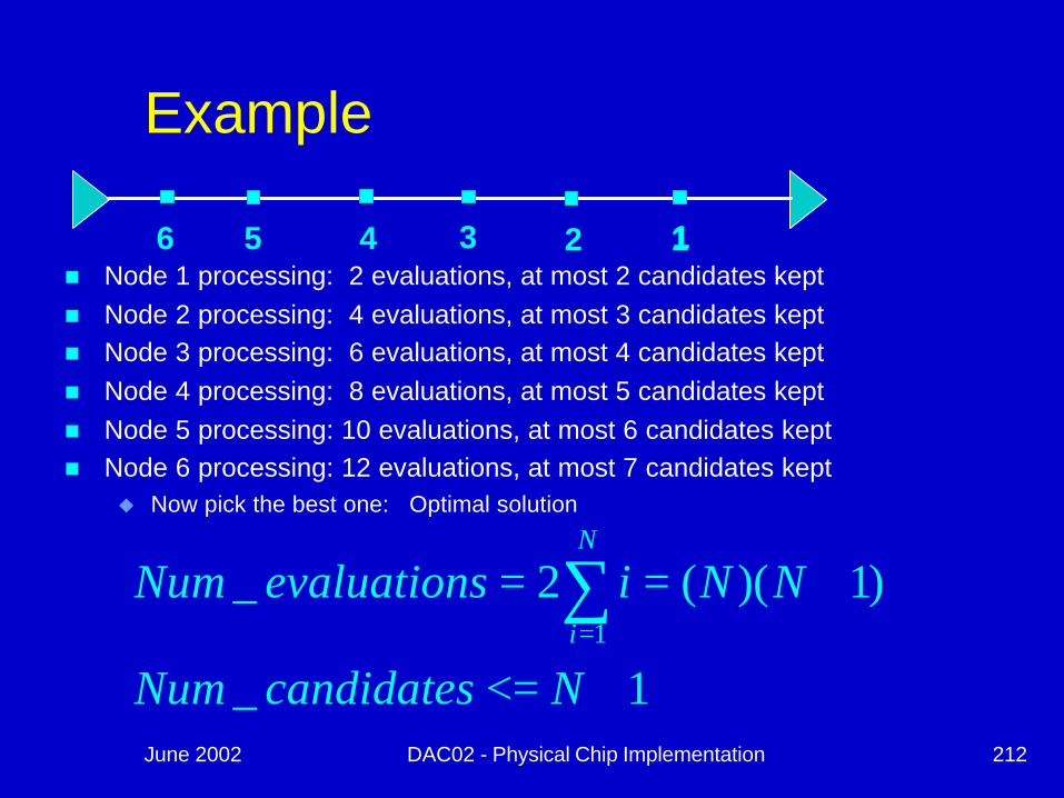
12 16 4 35
June 2002 DAC02 - Physical Chip Implementation 212
Example
12 16 4 35n Node 1 processing: 2 evaluations, at most 2 candidates kept n Node 2 processing: 4 evaluations, at most 3 candidates keptn Node 3 processing: 6 evaluations, at most 4 candidates keptn Node 4 processing: 8 evaluations, at most 5 candidates keptn Node 5 processing: 10 evaluations, at most 6 candidates keptn Node 6 processing: 12 evaluations, at most 7 candidates kept
u Now pick the best one: Optimal solution
1_
)1)((2_1
+<=
+== ∑=
NcandidatesNum
NNisevaluationNumN
i
June 2002 DAC02 - Physical Chip Implementation 213
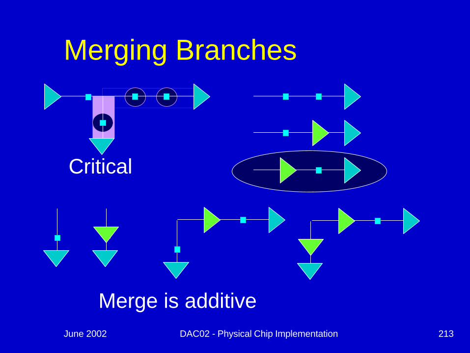
Merging Branches
Critical
Merge is additive

June 2002 DAC02 - Physical Chip Implementation 214
Van Ginneken Algorithm Summaryn GooduClever pruning controls # of candidatesu Finds an optimal solution in quadratic timeuEasily extended to cover a variety of important
considerations (like multiple buffer types, wire sizing, polarity, slew, & capacitance constraints, etc.
n BaduResults depend on quality of route provided

June 2002 DAC02 - Physical Chip Implementation 215
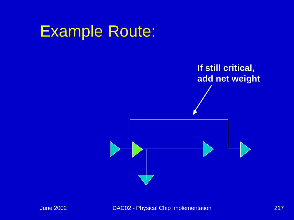
Example Route:Critical: can not offloaddue to route
Different route leadsto better solution

June 2002 DAC02 - Physical Chip Implementation 216
Physical Synthesis FlowSynthesized NetlistWire-load Models
UnplacedPhysically “unaware” timing
Cleanup: Remove buffers, nominal power levels on gates
Initial “basic” placementFor minimal wire-length, min-cut, Steiner tree estimates, physically aware timing
Logical + Placement optimizations
Timing-driven placement w/resynthesis
For minimal netweights, based on the timing of the net
Physically aware logic optimizations
Timing Improvement
?
Placed Netlist
Yes No more
June 2002 DAC02 - Physical Chip Implementation 217
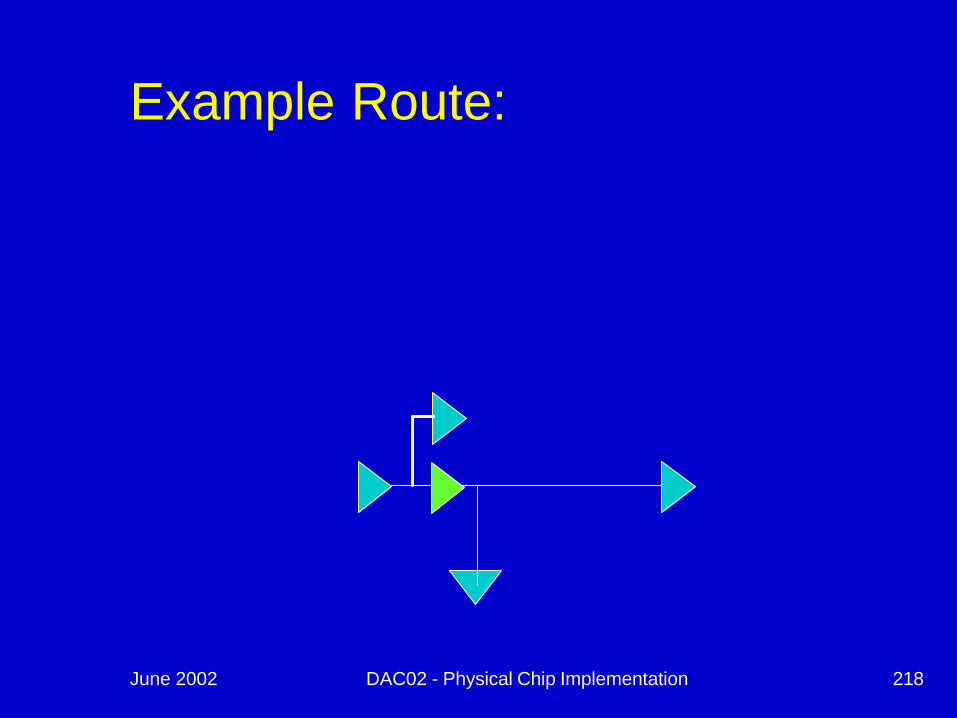
Example Route:
If still critical, add net weight
June 2002 DAC02 - Physical Chip Implementation 218
Example Route:

June 2002 DAC02 - Physical Chip Implementation 219
Multiple Buffer Types
n Instead of one buffer type, can choose from m power levels
n Generate m candidates instead of onen Still optimaln Complexity increase quadratic in m
June 2002 DAC02 - Physical Chip Implementation 220
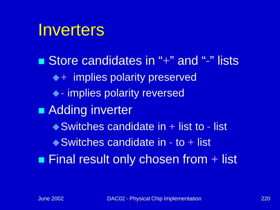
Inverters
n Store candidates in “+” and “-” listsu+ implies polarity preservedu- implies polarity reversed
n Adding inverteruSwitches candidate in + list to - listuSwitches candidate in - to + list
n Final result only chosen from + list
June 2002 DAC02 - Physical Chip Implementation 221
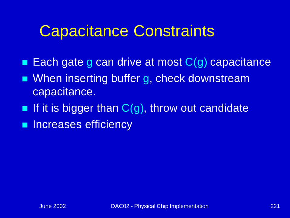
Capacitance Constraints
n Each gate g can drive at most C(g) capacitancen When inserting buffer g, check downstream
capacitance. n If it is bigger than C(g), throw out candidaten Increases efficiency

June 2002 DAC02 - Physical Chip Implementation 222
Slew Constraints
n Similar to capacitance constraintsn When inserting buffer, compute slews to
gates driven by buffern If any slew exceeds its target, throw out
candidaten Potential difficulty: computing slew accurately
in bottom-up fashion

June 2002 DAC02 - Physical Chip Implementation 223
Noise Constraints
n Each gate has acceptable noise thresholdn Compute cumulative noise for each wire via
Devgan noise metricn Throw out candidates that violate noise
Can avoid noise while optimizing timing!

June 2002 DAC02 - Physical Chip Implementation 224
Wire Sizing:
For each node (bottom up traversal of graph){
for each Wire Size{
augment each item in list with Sized wire segmentduplicate the listfor each element of the duplicate list
add a buffer at nodeanalyze each element in listanalyze each element in buffered (duplicate) listpick best element of buffered list and delete the restnew list is union of list and “best” element of buffered list
}} Do Final pruning & Pick best solution;
12 16 4 35
June 2002 DAC02 - Physical Chip Implementation 225
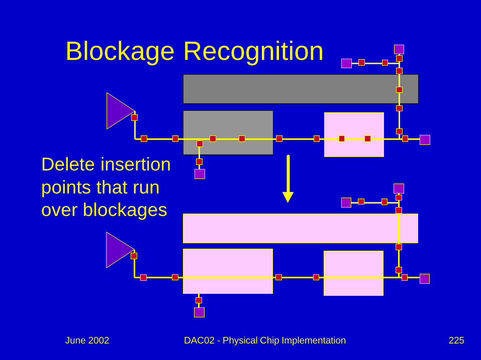
Blockage Recognition
Delete insertion points that run over blockages

June 2002 DAC02 - Physical Chip Implementation 226
Route Around Blockage
June 2002 DAC02 - Physical Chip Implementation 227
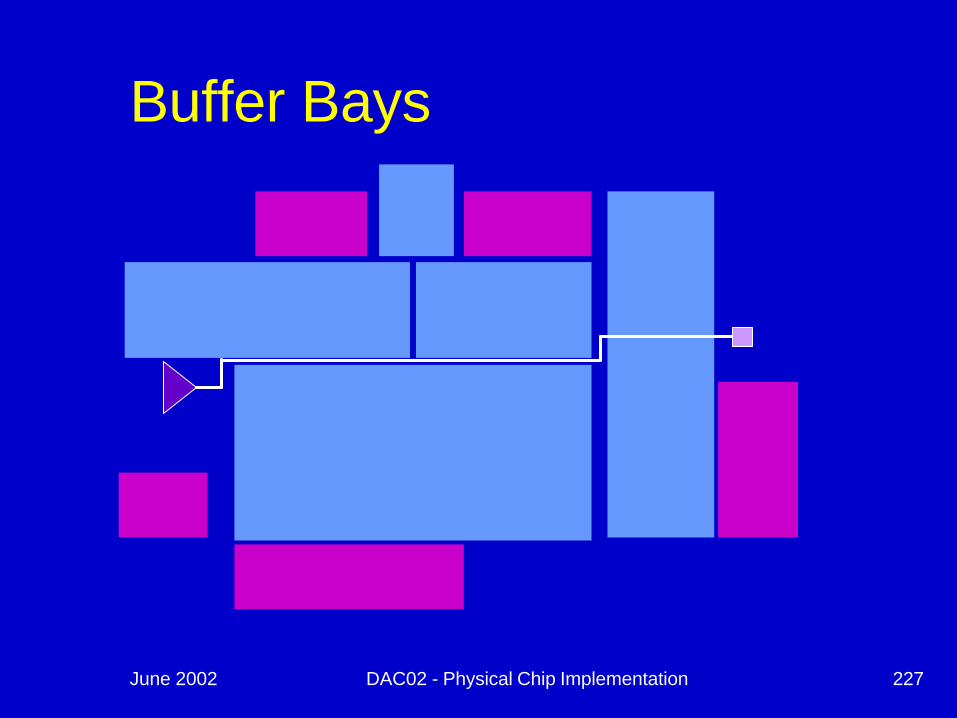
Buffer Bays

June 2002 DAC02 - Physical Chip Implementation 228
Routing Into Buffer Bays
June 2002 DAC02 - Physical Chip Implementation 229
“Buffer Site”n Similar to buffer bays, only exact buffer
locations are pre-specified, not just areasn Useful as a mechanism for IP blocks and
microprocessor designn Dummy cell that holds a buffern Not connected to any netn Becomes buffer when assigned to a netn Extra sites à decoupling capsn Sprinkle sites throughout designn Allocate percentage within macros
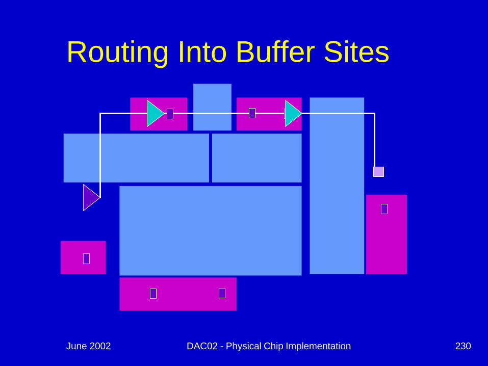
June 2002 DAC02 - Physical Chip Implementation 230
Routing Into Buffer Sites
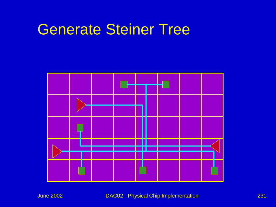
June 2002 DAC02 - Physical Chip Implementation 231
Generate Steiner Tree

June 2002 DAC02 - Physical Chip Implementation 232
Reduce Congestion and Coupling
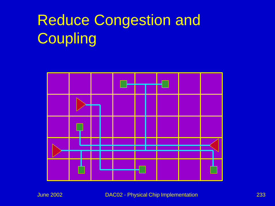
June 2002 DAC02 - Physical Chip Implementation 233
Reduce Congestion and Coupling

June 2002 DAC02 - Physical Chip Implementation 234
Assign Buffers
June 2002 DAC02 - Physical Chip Implementation 235
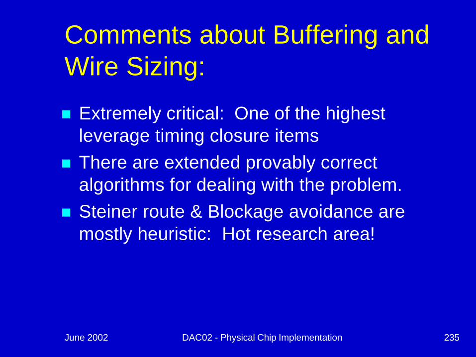
Comments about Buffering and Wire Sizing:
n Extremely critical: One of the highest leverage timing closure items
n There are extended provably correct algorithms for dealing with the problem.
n Steiner route & Blockage avoidance are mostly heuristic: Hot research area!

June 2002 DAC02 - Physical Chip Implementation 236
Section Outlinen Introductionn Review material (timing and synthesis)n Introduction to placementn Placement algorithmsn Paradigms for placement-synthesis
integrationn Placement aware synthesis techniquesn Congestion avoidance / mitigation techniquesn Routing Optimization

June 2002 DAC02 - Physical Chip Implementation 237
Congestion Mitigation
June 2002 DAC02 - Physical Chip Implementation 238
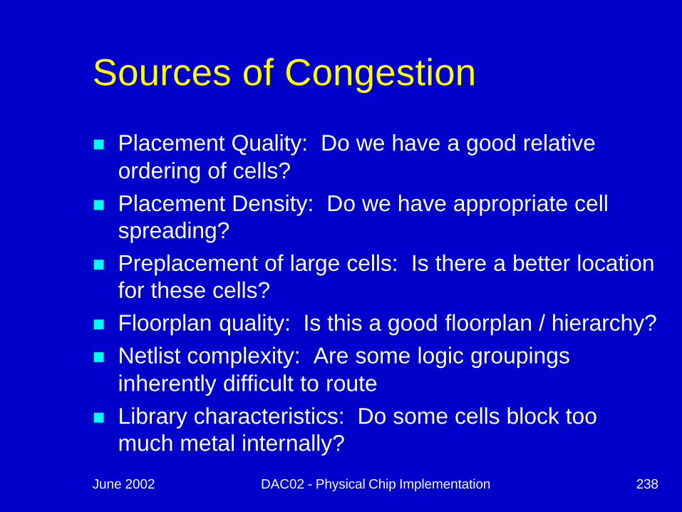
Sources of Congestion
n Placement Quality: Do we have a good relative ordering of cells?
n Placement Density: Do we have appropriate cell spreading?
n Preplacement of large cells: Is there a better location for these cells?
n Floorplan quality: Is this a good floorplan / hierarchy?n Netlist complexity: Are some logic groupings
inherently difficult to routen Library characteristics: Do some cells block too
much metal internally?

June 2002 DAC02 - Physical Chip Implementation 239
Congestion Mitigation
n Constructive Avoidanceucontrol global placement pin density: fewer
pins per unit area means fewer wires per unit area
umonitor congestion during placement and perform dynamic spreading
n Post placement fix upuremove problems from an already placed
netlist
June 2002 DAC02 - Physical Chip Implementation 240
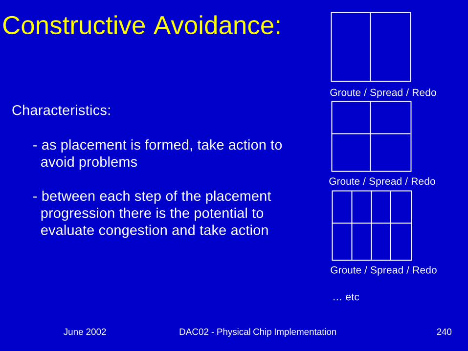
Groute / Spread / Redo
Constructive Avoidance:
Characteristics:
- as placement is formed, take action to avoid problems
- between each step of the placementprogression there is the potential to evaluate congestion and take action
Groute / Spread / Redo
Groute / Spread / Redo
… etc

June 2002 DAC02 - Physical Chip Implementation 241
Constructive Avoidance Deficiencies:n Depends on early estimates of congestion
that may not be accurate enough to avoid all problems
n Post placement actions such as clock tree insertion, repowering, buffering, etc may add congestion too the design
n Guard banding with conservative “constructive avoidance” causes lose of performance and density
June 2002 DAC02 - Physical Chip Implementation 242
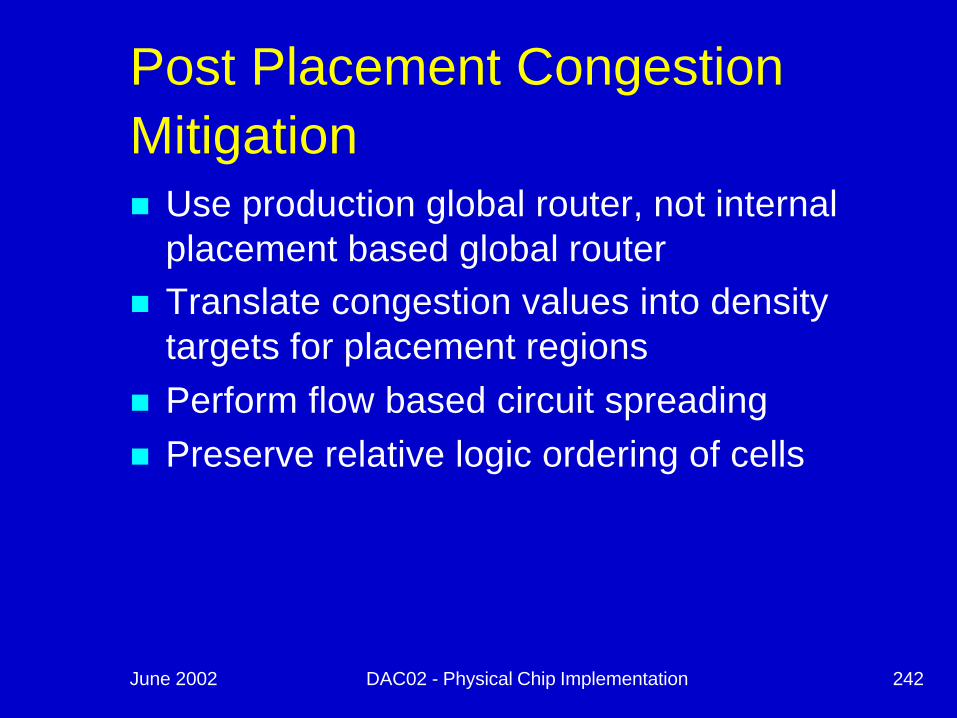
Post Placement Congestion Mitigationn Use production global router, not internal
placement based global routern Translate congestion values into density
targets for placement regionsn Perform flow based circuit spreadingn Preserve relative logic ordering of cells

June 2002 DAC02 - Physical Chip Implementation 243
Network Flow based Spreading
Supply Nodes Demand Nodes
s t
i j
b(i) > 0 b(j) < 0
ÙMin-cost max-flow formulation
¼ i if b(i) > 0,Cap(esi) = b(i)
Cost(esi) = 0
¼ i ! s , j ! t, Cap(eij) = Infinity (Large Int)Cost(eij) = K
¼ j if b(j) < 0,Cap(ejt) = -b(j)Cost(ejt) = 0
June 2002 DAC02 - Physical Chip Implementation 244
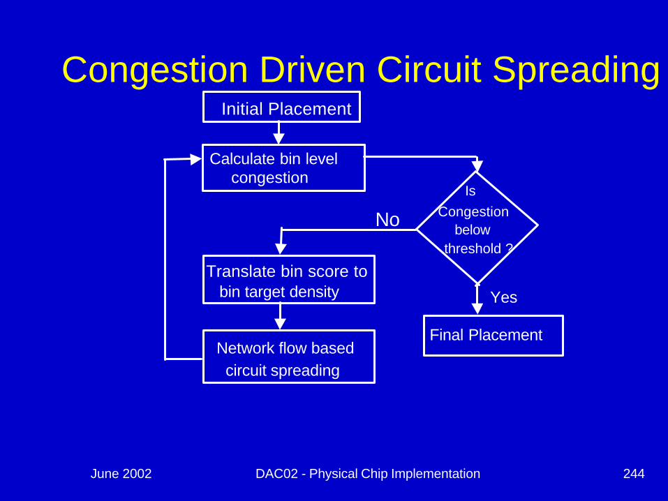
Initial Placement
Calculate bin levelcongestion
Is Congestion
belowthreshold ?
Translate bin score tobin target density
Network flow based circuit spreading
Final Placement
Congestion Driven Circuit Spreading
Yes
No

June 2002 DAC02 - Physical Chip Implementation 245

June 2002 DAC02 - Physical Chip Implementation 246
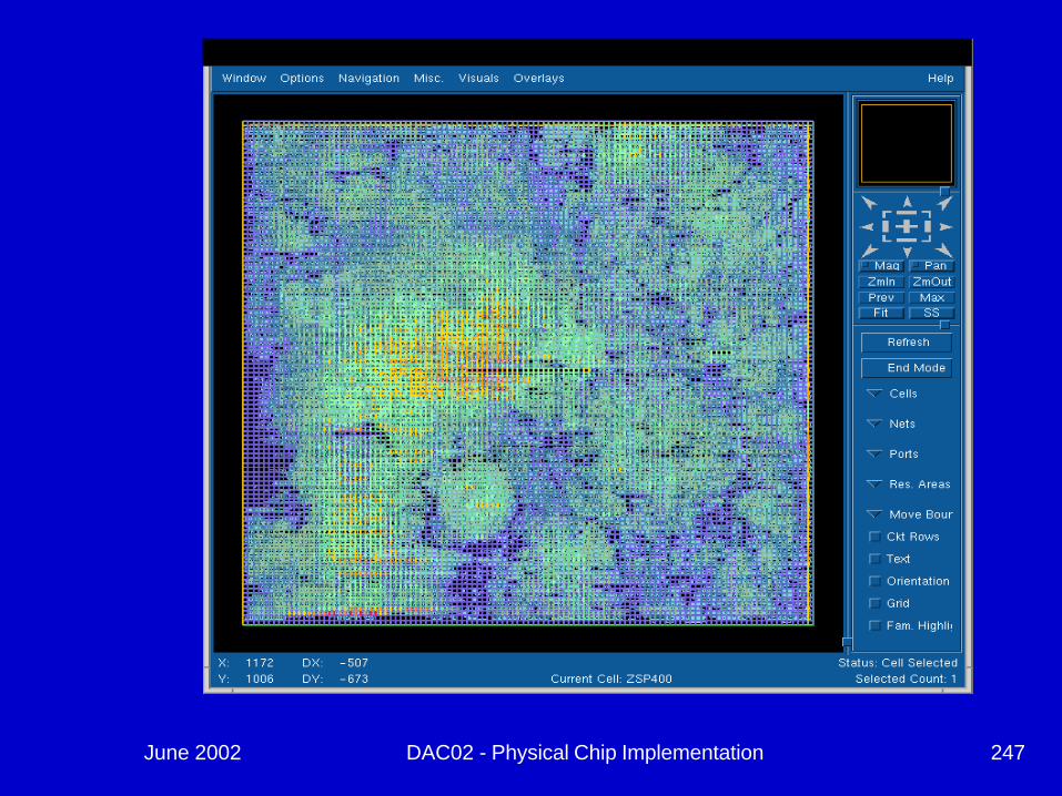
June 2002 DAC02 - Physical Chip Implementation 247
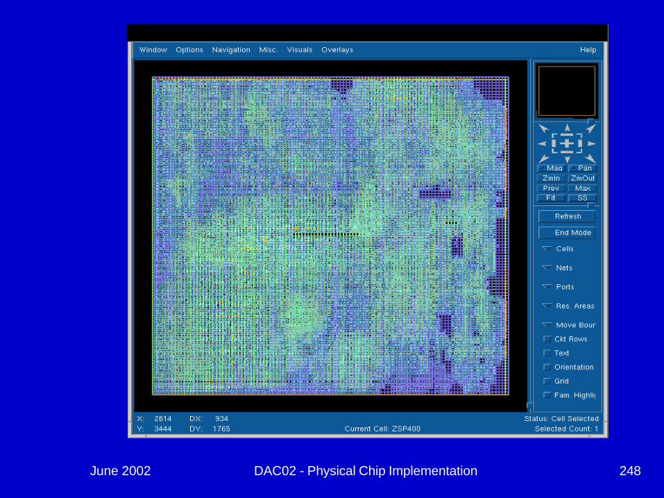
June 2002 DAC02 - Physical Chip Implementation 248

June 2002 DAC02 - Physical Chip Implementation 249
We’ve Talked About
n Placement algorithmsn Placement / Synthesis interactionn Placement aware synthesis techniquesn The Constant Delay paradigmn Physical Buffer insertion / Wire sizingn Congestion Mitigation
June 2002 DAC02 - Physical Chip Implementation 250
Let’s Look at some Examples:
June 2002 DAC02 - Physical Chip Implementation 251
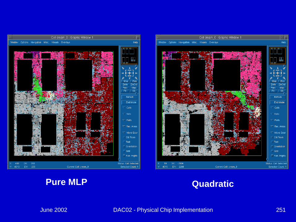
Pure MLP Quadratic

June 2002 DAC02 - Physical Chip Implementation 252
shatterclonefaninbuffer
Optimization Results

June 2002 DAC02 - Physical Chip Implementation 253
Optimization Results
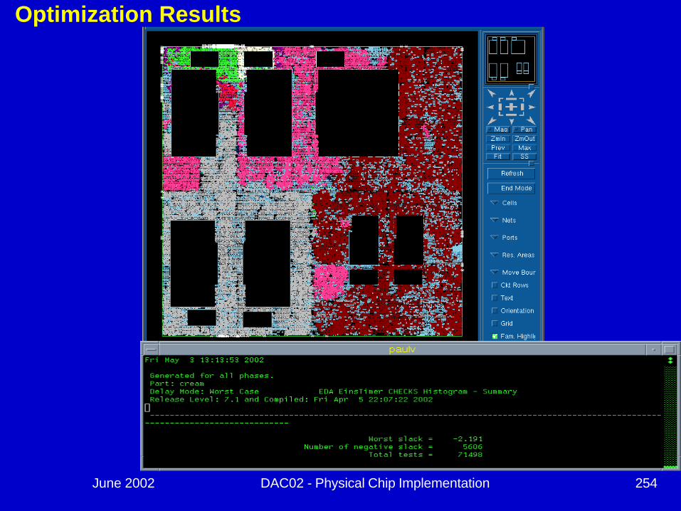
June 2002 DAC02 - Physical Chip Implementation 254
Optimization Results

June 2002 DAC02 - Physical Chip Implementation 255
Section outlinen Introductionn Review material (timing and synthesis)n Introduction to placementn Placement algorithmsn Paradigms for placement-synthesis
integrationn Placement aware synthesis techniquesn Congestion avoidance / mitigation techniquesn Routing optimization
June 2002 DAC02 - Physical Chip Implementation 256
Routing Based Optimization: RBO (IBM)

June 2002 DAC02 - Physical Chip Implementation 257
Routing based Timing Closure Issuesn Post Routing timing problems can be significantu affect design scheduleumay be too numerous to fix manually
n Increasing design density can reduce cost, but it also increases wiring congestionu timing and signal integrity become more significantu available resource for manual fixup is limiteduwithout automation may not be doable
n Rerouting with constraints may resolve some of the problems, but this process is slow

June 2002 DAC02 - Physical Chip Implementation 258
Solution:
n Integrate global routing, detailed routing and timing correction
n Global routing is efficient enough to be run in an iterative timing closure loop
n Timing critical nets avoid scenic routesn Non-critical nets that go scenic can be
repowered and buffered prior to detailed routing
June 2002 DAC02 - Physical Chip Implementation 259
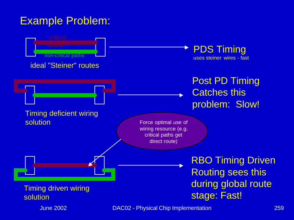
critical critical pathspaths
non-critical pathsPDS Timinguses steiner wires - fast
ideal "Steiner" routes
Timing deficient wiring solution
Post PD Timing Catches this problem: Slow!
Timing driven wiring solution
RBO Timing Driven Routing sees this during global route stage: Fast!
Force optimal use of wiring resource (e.g.
critical paths get direct route)
Example Problem:

June 2002 DAC02 - Physical Chip Implementation 260
Global RoutingDivides the entire chip into localized rectangular regions called tiles.
Compress several pin location in each tile to a single pin location
All the shapes, wires and open are represented in terms of globaltrack capacity and usage.
June 2002 DAC02 - Physical Chip Implementation 261
Global Routing
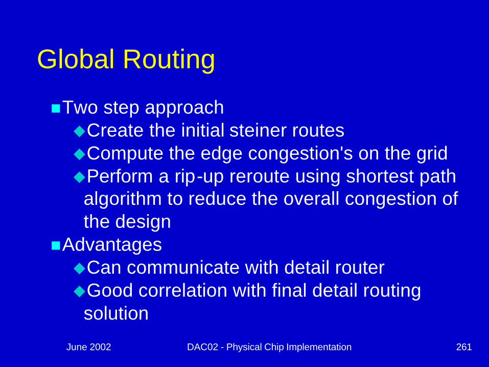
nTwo step approachuCreate the initial steiner routesuCompute the edge congestion's on the griduPerform a rip-up reroute using shortest path
algorithm to reduce the overall congestion of the design
nAdvantagesuCan communicate with detail routeruGood correlation with final detail routing
solution

June 2002 DAC02 - Physical Chip Implementation 262
Current Methodology
Physical Synthesis
Global Routing
Detailed Routing
Timing Analysis
RBO Methodology
Physical Synthesis
RBO / Physical
Synthesis
Detailed Routing
Analysis
XrGlobal
Extractor Optimizer
Einstimer
No Timing Criticality for Global router
Costly Manual Timing Correction
Routing Based Optimization

June 2002 DAC02 - Physical Chip Implementation 263
RBO Extraction Process
nVery fast uExcellent correlation with final 3D extraction
nUses global routes for extractionnNeighbor information probabilistically determined based on
the global routing congestion informationnBased on extraction tables
Capacity of All Edges = 5
Probability of having a neighbor = (#OccupiedTracks)/(#Capacity) = 2/4 = 0.5
1
3 3 2
June 2002 DAC02 - Physical Chip Implementation 264
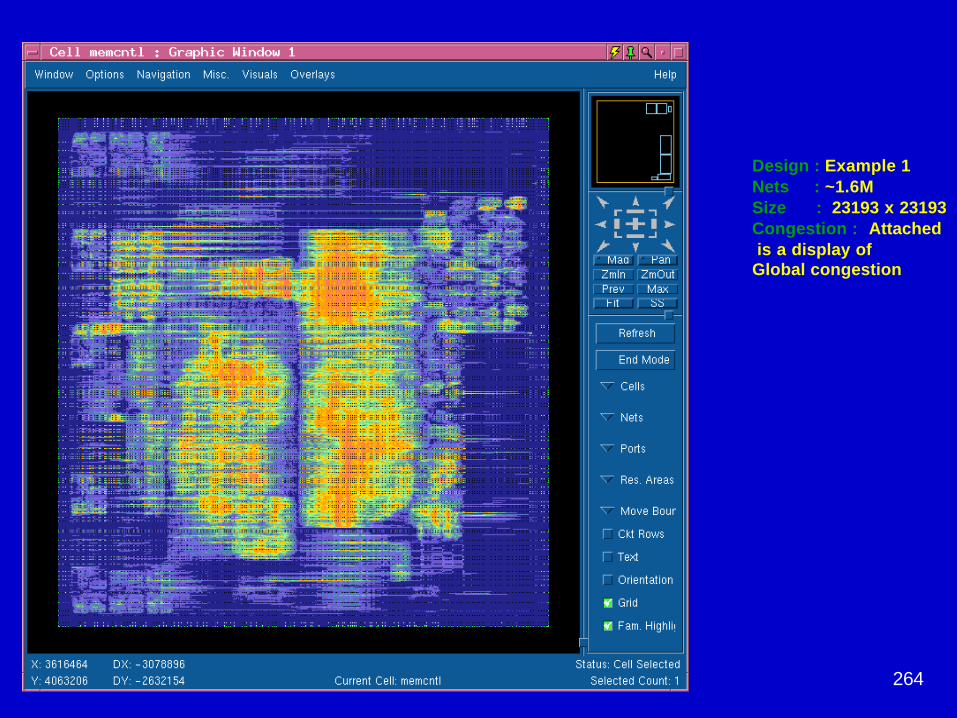
RBO results onRBO results on memcntlmemcntlDesign : Example 1Nets : ~1.6MSize : 23193 x 23193Congestion : Attached is a display of
Global congestion

June 2002 DAC02 - Physical Chip Implementation 265
Timing Critical Nets: Without RBO
June 2002 DAC02 - Physical Chip Implementation 266
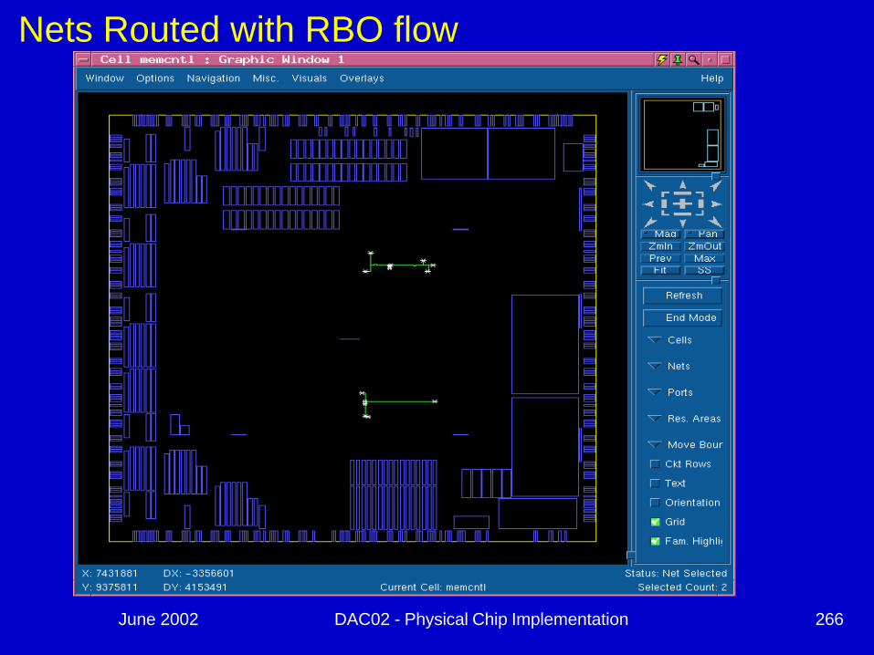
Nets Routed with RBO flow
June 2002 DAC02 - Physical Chip Implementation 267
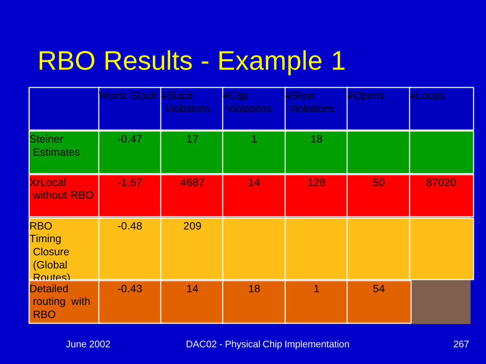
RBO Results - Example 1Worst Slack #Slack
Violations#Cap Violations
#Slew Violations
#Opens #Loops
Steiner Estimates
-0.47 17 1 18
XrLocalwithout RBO
-1.57 4687 14 128 50 87020
RBO Timing Closure (Global Routes)
-0.48 209
Detailed routing with RBO
-0.43 14 18 1 54
June 2002 DAC02 - Physical Chip Implementation 268
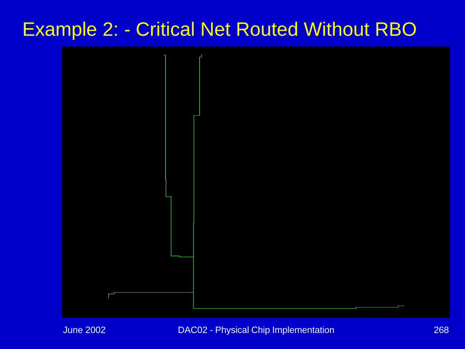
Example 2: - Critical Net Routed Without RBO
June 2002 DAC02 - Physical Chip Implementation 269
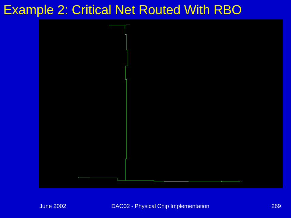
Example 2: Critical Net Routed With RBO
June 2002 DAC02 - Physical Chip Implementation 270
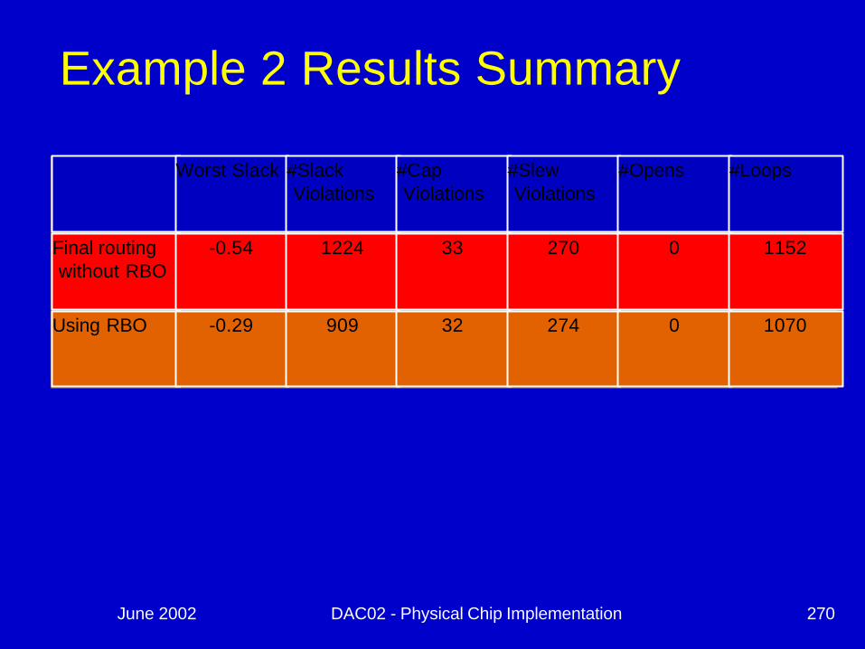
Example 2 Results Summary
Worst Slack #Slack Violations
#Cap Violations
#Slew Violations
#Opens #Loops
Final routing without RBO
-0.54 1224 33 270 0 1152
Using RBO -0.29 909 32 274 0 1070
June 2002 DAC02 - Physical Chip Implementation 271
PDS - RBO Integration
No
t No
ise Aw
are
No
ise Aw
are
112
2
3
4
56
7
8
9
10
11
11 2
23
45
678
9
10
11
Steiner Routes Timing Closure
PDS-Einstimer
Current Flow
Timing SignOff
ChipEdit-Einstimer
Detail Routing
Xrouter
No
No
iseS
ign
Off
Probabilistic Detection of Noise Problems
PDS-Einstimer-RBO
Noise Avoidance
PDS-Einstimer-RBO
SignOff Noise Detection
ETCoupling-3DNoise
Noise Correction
Manual Correction
Timing Closure
PDS-Einstimer-RBO
Steiner-Global
Projected Flow
Steiner Routes Timing Closure
PDS-Einstimer
Global Routes Timing Closure
RBO-Einstimer
SignOff Noise Detection
ETCoupling-3DNoise
Noise Correction
Manual Correction
Proposed Flow -Existing Tools

June 2002 DAC02 - Physical Chip Implementation 272
Noise Detection and Avoidance:n RBO (Detection)u Length Base
F Initial selection includes length and slack thresholdFFurther pruning based on Worst Case Miller
TiminguSwitching Window based refinement
FPattern generation based on switching window overlaps
n RBO (Avoidance)u Long Net Spreading u Track Reordering u Incremental Placement Changes u Layer Assignment
June 2002 DAC02 - Physical Chip Implementation 273
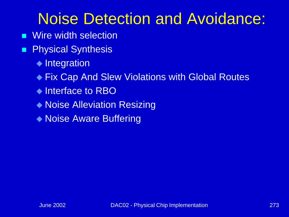
Noise Detection and Avoidance:n Wire width selectionn Physical Synthesisu Integrationu Fix Cap And Slew Violations with Global Routes u Interface to RBO uNoise Alleviation Resizing uNoise Aware Buffering

June 2002 DAC02 - Physical Chip Implementation 274
Long Net Spreader
June 2002 DAC02 - Physical Chip Implementation 275
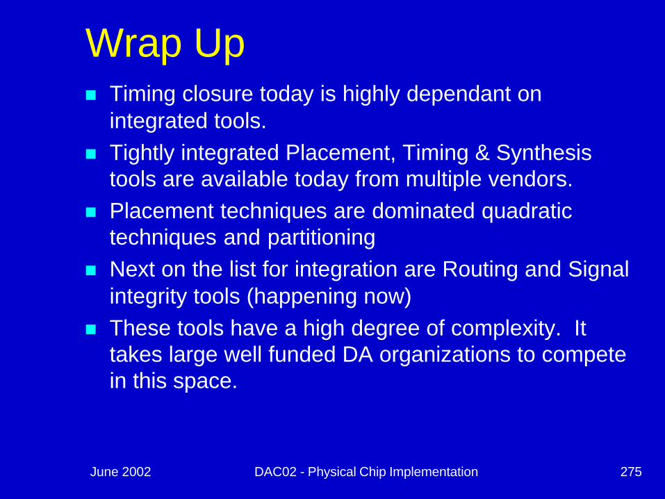
Wrap Upn Timing closure today is highly dependant on
integrated tools.n Tightly integrated Placement, Timing & Synthesis
tools are available today from multiple vendors.n Placement techniques are dominated quadratic
techniques and partitioningn Next on the list for integration are Routing and Signal
integrity tools (happening now) n These tools have a high degree of complexity. It
takes large well funded DA organizations to compete in this space.

June 2002 DAC02 - Physical Chip Implementation 276
Placement Referencesnn C. J. Alpert, T. Chan, D. J.C. J. Alpert, T. Chan, D. J.--H,H,\\. Huang, I. Markov, and K. . Huang, I. Markov, and K. YanYan, “, “Quandratic Quandratic
Placement Revisited”,Proc. 34th IEEE/ACM Design Automation ConfePlacement Revisited”,Proc. 34th IEEE/ACM Design Automation Conference, 1997, rence, 1997, pp. 752pp. 752--757757
nn C. J. Alpert, J.C. J. Alpert, J.--H Huang, and A. B. Kahng, “Multilevel Circuit Partitioning”, ProH Huang, and A. B. Kahng, “Multilevel Circuit Partitioning”, Proc. 34th c. 34th IEEE/ACM Design Automation Conference, 1997, pp. 530IEEE/ACM Design Automation Conference, 1997, pp. 530--533533
nn U. Brenner, and A. U. Brenner, and A. RoheRohe, “An Effective Congestion Driven Placement Framework”, , “An Effective Congestion Driven Placement Framework”, International Symposium on Physical Design 2002, pp. 6International Symposium on Physical Design 2002, pp. 6--1111
nn A. E. Caldwell, A. B. Kahng, and I.L. Markov, “Can Recursive BisA. E. Caldwell, A. B. Kahng, and I.L. Markov, “Can Recursive Bisection Alone ection Alone Produce Routable Placements”,Proc. 37th IEEE/ACM Design AutomatiProduce Routable Placements”,Proc. 37th IEEE/ACM Design Automation Conference, on Conference, 2000, 2000, pp pp 477477--482482
nn M.A. M.A. BreuerBreuer, “Min, “Min--Cut Placement”, J. Design Automation and Fault Tolerant Cut Placement”, J. Design Automation and Fault Tolerant Computing, I(4), 1997, Computing, I(4), 1997, pp pp 343343--362362
nn J. J. VygenVygen, “Algorithms for Large, “Algorithms for Large--Scale Flat Placement”, Scale Flat Placement”, ProcProc. 34th IEEE/ACM Design . 34th IEEE/ACM Design Automation Conference, 1988,Automation Conference, 1988,pp pp 746746--751751
nn H. H. Eisenmann Eisenmann and F. M. Johannes, “Generic Global Placement and and F. M. Johannes, “Generic Global Placement and FloorplanningFloorplanning”, ”, ProcProc. 35th IEEE/ACM Design Automation Conference, 1998, . 35th IEEE/ACM Design Automation Conference, 1998, pppp. 269. 269--274274
nn S.S.--L. L. Ou Ou and M. and M. PedramPedram, “Timing Driven Placement Based on Partitioning with , “Timing Driven Placement Based on Partitioning with Dynamic CutDynamic Cut--Net Control”, Net Control”, ProcProc. 37th IEEE/ACM Design Automation Conference, . 37th IEEE/ACM Design Automation Conference, 2000, 2000, pppp. 472. 472--476476
nn C.M. C.M. Fiduccia Fiduccia and R.M. and R.M. MattheysesMattheyses, A linear time heuristic for improving network , A linear time heuristic for improving network partitions, partitions, ProcProc. ACM/IEEE Design Automation Conference. (1982) . ACM/IEEE Design Automation Conference. (1982) pppp. 175 . 175 -- 181.181.

June 2002 DAC02 - Physical Chip Implementation 277
Synthesis Referencesnn C.L. Berman, J. L. Carter, and K.F. Day. The C.L. Berman, J. L. Carter, and K.F. Day. The Fanout Fanout Problem: From Theory to Practice. In Problem: From Theory to Practice. In
Advanced Research in VLSI: Proceedings of the 1989 Decennial CaAdvanced Research in VLSI: Proceedings of the 1989 Decennial Caltech Conference, pages ltech Conference, pages 6969--99, 198999, 1989
nn C. L. Berman, D. J. Hathaway, A. S. C. L. Berman, D. J. Hathaway, A. S. LaPaughLaPaugh, and L. H. , and L. H. TrevillyanTrevillyan. Efficient Techniques for . Efficient Techniques for Timing Corrections. In International Symposium on Circuits and Timing Corrections. In International Symposium on Circuits and Systems, Pages 415Systems, Pages 415--419, 1990419, 1990
nn F. F. BeeftingBeefting, P. N. , P. N. KudvaKudva, D. S. Kung, R. , D. S. Kung, R. PuriPuri, and L. , and L. StokStok. Combinatorial Cell Design for CMOS . Combinatorial Cell Design for CMOS Libraries INTEGRATION, the VLSI Journal, 29:67Libraries INTEGRATION, the VLSI Journal, 29:67--93, 200093, 2000
nn W. W. DonathDonath, P. , P. KudvaKudva, L. , L. StokStok, P. Villarrubia, L. Reddy, and A. Sullivan. Transformational , P. Villarrubia, L. Reddy, and A. Sullivan. Transformational placement and synthesis. In DATE, pages 194placement and synthesis. In DATE, pages 194--201, 2000201, 2000
nn D. J. Hathaway, R.P. D. J. Hathaway, R.P. AbatoAbato, A.D. , A.D. DrummDrumm, and L.P.P.P . Van , and L.P.P.P . Van GinnekenGinneken. Incremental timing . Incremental timing analysis. Technical report, IBM Corp., 1996. U.S. patent 5,508analysis. Technical report, IBM Corp., 1996. U.S. patent 5,508,937.,937.
nn D. Kung, P. D. Kung, P. KudvaKudva, and A. Sullivan. A Gate Sizing Algorithm using Geometric Prog, and A. Sullivan. A Gate Sizing Algorithm using Geometric Programming. In ramming. In ProcProc. Of the International Workshop on Logic Synthesis, 1997. Of the International Workshop on Logic Synthesis, 1997
nn T. T. Kutzschebauch Kutzschebauch and L. and L. StokStok. Regularity driven logic synthesis. In . Regularity driven logic synthesis. In Proc Proc of the of the IntInt. . ConfConf. On . On Computer Aided Design, Nov 2000.Computer Aided Design, Nov 2000.
nn P. P. RezvaniRezvani, A.H. , A.H. AjamiAjami, M. , M. PedramPedram, and H. , and H. SavojSavoj. LEOPARD: A Logical Effort based . LEOPARD: A Logical Effort based fanout fanout Optimizer for Area and Delay. In IEEE/ACM International ConfereOptimizer for Area and Delay. In IEEE/ACM International Conference on CAD, pages 516nce on CAD, pages 516--519, 519, 1999.1999.
nn L. L. StokStok, M. , M. IyerIyer, and A. Sullivan. , and A. Sullivan. Wavefront Wavefront technology mapping. In DATE, pages 531technology mapping. In DATE, pages 531--536, 536, 19991999
nn D. S. Kung. A Fast D. S. Kung. A Fast Fanout Fanout Optimization for NewOptimization for New--Continuous Buffer Libraries. In IEEE/ACM Continuous Buffer Libraries. In IEEE/ACM Design Automation Conference, pages 352Design Automation Conference, pages 352--355, 1998355, 1998

June 2002 DAC02 - Physical Chip Implementation 278
DP Buffer Insertion References
nn Buffer placement in distributed RCBuffer placement in distributed RC--tree networks for minimal Elmore delay tree networks for minimal Elmore delay van van GinnekenGinneken, L.P.P.P. Circuits and Systems, 1990., IEEE International , L.P.P.P. Circuits and Systems, 1990., IEEE International Symposium on , 1990 Page(s): 865 Symposium on , 1990 Page(s): 865 --868 vol.2868 vol.2
nn Optimal wire sizing and buffer insertion for low power and a genOptimal wire sizing and buffer insertion for low power and a generalized delay eralized delay modelmodel LillisLillis, J.; Chung, J.; Chung--KuanKuan Cheng; Lin, T.Cheng; Lin, T.--T.Y. SolidT.Y. Solid--State Circuits, IEEE State Circuits, IEEE Journal of , Volume: 31 Issue: 3 , March 1996 Page(s): 437 Journal of , Volume: 31 Issue: 3 , March 1996 Page(s): 437 ––447447
nn Buffer insertion for noise and delay optimization Alpert, C.J.;Buffer insertion for noise and delay optimization Alpert, C.J.; DevganDevgan, A.; , A.; Quay, S.T. ComputerQuay, S.T. Computer--Aided Design of Integrated Circuits and Systems, IEEE Aided Design of Integrated Circuits and Systems, IEEE Transactions on , Volume: 18 Issue: 11 , Nov. 1999 Page(s): 1633Transactions on , Volume: 18 Issue: 11 , Nov. 1999 Page(s): 1633 --16451645
nn Buffer insertion with accurate gate and interconnect delay compuBuffer insertion with accurate gate and interconnect delay computation Alpert, tation Alpert, C.J.;C.J.; DevganDevgan, A.; Quay, S.T. Design Automation Conference, 1999. , A.; Quay, S.T. Design Automation Conference, 1999. Proceedings. 36th , 1999 Page(s): 479 Proceedings. 36th , 1999 Page(s): 479 ––484484
nn Wire Segmenting For Improved Buffer Insertion Alpert, C.;Wire Segmenting For Improved Buffer Insertion Alpert, C.; DevganDevgan, A. Design , A. Design Automation Conference, 1997. Proceedings of the 34th Page(s): 58Automation Conference, 1997. Proceedings of the 34th Page(s): 588 8 ––593593
nn Simultaneous routing and buffer insertion for high performance iSimultaneous routing and buffer insertion for high performance interconnectnterconnectLillisLillis, J.; Chung, J.; Chung--KuanKuan Cheng; TingCheng; Ting--Ting Y. Lin VLSI, 1996. Proceedings., Sixth Ting Y. Lin VLSI, 1996. Proceedings., Sixth Great Lakes Symposium on , 1996 Page(s): 148 Great Lakes Symposium on , 1996 Page(s): 148 --153153

June 2002 DAC02 - Physical Chip Implementation 279
Blockage Avoidance References
nn Steiner tree optimization for buffers, blockages, and bays AlperSteiner tree optimization for buffers, blockages, and bays Alpert, C.J.;t, C.J.; GandhamGandham, G.;, G.;Jiang HuJiang Hu;; NevesNeves, J.I.; Quay, S.T.;, J.I.; Quay, S.T.; SapatnekarSapatnekar, S.S. Computer, S.S. Computer--Aided Design of Aided Design of Integrated Circuits and Systems, IEEE Transactions on , Volume: Integrated Circuits and Systems, IEEE Transactions on , Volume: 20 Issue: 4 , April 20 Issue: 4 , April 2001 Page(s): 556 2001 Page(s): 556 ––562.562.
nn A fast algorithm for contextA fast algorithm for context--aware buffer insertion aware buffer insertion JagannathanJagannathan, A.; , A.; SungSung--WooWoo HurHur;; LillisLillis, J. Design Automation Conference, 2000. , J. Design Automation Conference, 2000. Proceedings 2000 Page(s): 368 Proceedings 2000 Page(s): 368 ––373.373.
nn Simultaneous routing and buffer insertion with restrictions on bSimultaneous routing and buffer insertion with restrictions on buffer uffer locationslocations Hai ZhouHai Zhou; Wong, D.F.; I; Wong, D.F.; I--Min Liu;Min Liu; AzizAziz, A. Computer, A. Computer--Aided Aided Design of Integrated Circuits and Systems, IEEE Transactions on Design of Integrated Circuits and Systems, IEEE Transactions on , , Volume: 19 Issue: 7 , July 2000 Page(s): 819 Volume: 19 Issue: 7 , July 2000 Page(s): 819 --824824
nn Maze routing with buffer insertion and wire sizing Maze routing with buffer insertion and wire sizing MinghorngMinghorng Lai; Wong, Lai; Wong, D.F. Design Automation Conference, 2000. Proceedings 2000 Page(sD.F. Design Automation Conference, 2000. Proceedings 2000 Page(s): ): 374 374 --378378
nn Routing tree construction under fixed buffer locations Cong, J.;Routing tree construction under fixed buffer locations Cong, J.; XinXin Yuan Yuan Design Automation Conference, 2000. Proceedings 2000 Page(s): 37Design Automation Conference, 2000. Proceedings 2000 Page(s): 379 9 --384384

June 2002 DAC02 - Physical Chip Implementation 280
Interconnect Planning Referencesnn A practical methodology for early buffer and wire resource allocA practical methodology for early buffer and wire resource allocation Alpert, C.J.;ation Alpert, C.J.;
Jiang HuJiang Hu;; SapatnekarSapatnekar, S.S.;, S.S.; VillarrubiaVillarrubia, P.G. Design Automation Conference, 2001. , P.G. Design Automation Conference, 2001. Proceedings , 2001 Page(s): 189 Proceedings , 2001 Page(s): 189 ––194194
nn An interconnectAn interconnect--centric design flow for nanometer technologies Cong, J. Proceedicentric design flow for nanometer technologies Cong, J. Proceedings ngs of the IEEE , Volume: 89 Issue: 4 , April 2001 Page(s): 505 of the IEEE , Volume: 89 Issue: 4 , April 2001 Page(s): 505 --528528
nn Buffer block planning for interconnectBuffer block planning for interconnect--drivendriven floorplanningfloorplanning Cong, J.;Cong, J.; TianmingTianming Kong; Kong; Pan, D.Z. ComputerPan, D.Z. Computer--Aided Design, 1999. Digest of Technical Papers. 1999 Aided Design, 1999. Digest of Technical Papers. 1999 IEEE/ACM International Conference on , 1999 Page(s): 358 IEEE/ACM International Conference on , 1999 Page(s): 358 ––363363
nn Provably good global buffering using an available buffer block pProvably good global buffering using an available buffer block plan lan DraganDragan, F.F.;, F.F.;KahngKahng, A.B.;, A.B.; MandoiuMandoiu, I.;, I.; MudduMuddu, S.;, S.; ZelikovskyZelikovsky, A. Computer Aided Design, 2000. , A. Computer Aided Design, 2000. ICCADICCAD--2000. IEEE/ACM International Conference on , 2000 Page(s): 104 2000. IEEE/ACM International Conference on , 2000 Page(s): 104 --109109
nn Provably good global buffering byProvably good global buffering by multiterminal multicommoditymultiterminal multicommodity flow approximation flow approximation DraganDragan, F.F.;, F.F.; KahngKahng, A.B.;, A.B.; MandoiuMandoiu, I.;, I.; MudduMuddu, S.;, S.; ZelikovskyZelikovsky, A. Design , A. Design Automation Conference, 2001. Proceedings of the ASPAutomation Conference, 2001. Proceedings of the ASP--DAC 2001. Asia and South DAC 2001. Asia and South Pacific , 2001 Page(s): 120 Pacific , 2001 Page(s): 120 ––125125
nn Planning buffer locations by network flows Tang, X.; Wong, D.F.Planning buffer locations by network flows Tang, X.; Wong, D.F.; International ; International Symposium on Physical Design, April 2001 Page(s): 180Symposium on Physical Design, April 2001 Page(s): 180--185185
nn RoutabilityRoutability--Driven Repeater Block Planning for InterconnectDriven Repeater Block Planning for Interconnect--Centric Centric Floorplanning Floorplanning SarkarSarkar, P.; , P.; SundararamanSundararaman, V.; , V.; KohKoh, C., C.--K.; International Symposium on Physical K.; International Symposium on Physical Design, April 2001 Page(s): 186Design, April 2001 Page(s): 186--191191


