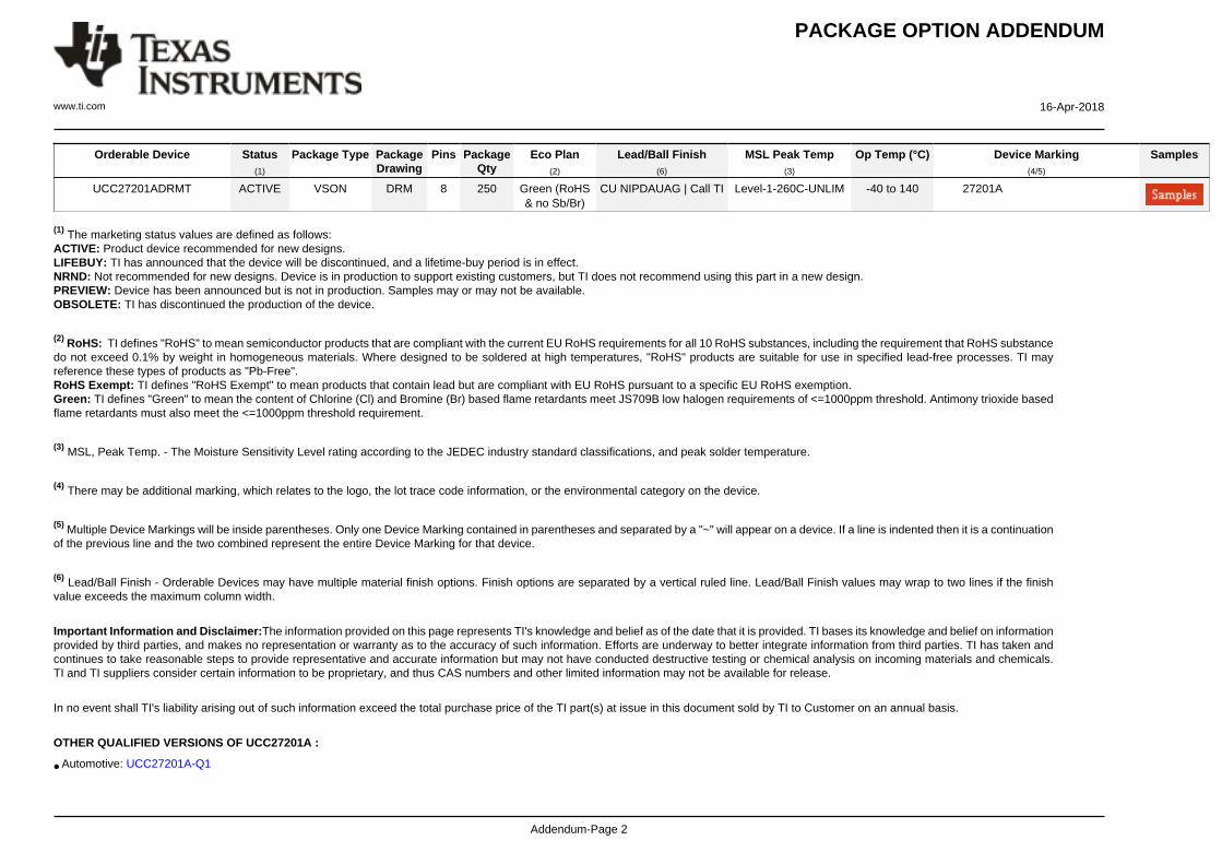
PWM CONTROLLER +12V ISOLATION AND FEEDBACK +100V SECONDARY SIDE CIRCUIT HI CONTROL DRIVE LO DRIVE HI VDD UCC27200A/1A VSS LI HB HO HS LO Product Folder Sample & Buy Technical Documents Tools & Software Support & Community UCC27200A, UCC27201A SLUSAF9B – FEBRUARY 2011 – REVISED JULY 2015 UCC2720xA 120-V Boot, 3-A Peak, High-Frequency, High-Side and Low-Side Driver 1 Features 3 Description The UCC2720xA family of high-frequency N-channel 1• Drives Two N-Channel MOSFETs in High-Side MOSFET drivers include a 120-V bootstrap diode and and Low-Side Configuration high-side/low-side driver with independent inputs for • Negative Voltage Handling on HS (–18V) maximum control flexibility. This allows for N-channel • Maximum Boot Voltage 120 V MOSFET control in half-bridge, full-bridge, two-switch forward and active clamp forward converters. The • Maximum VDD Voltage 20 V low-side and the high-side gate drivers are • On-Chip 0.65-V VF, 0.6-Ω RD Bootstrap Diode independently controlled and matched to 1-ns • Greater than 1 MHz of Operation between the turn-on and turn-off of each other. The UCC2720xA are based on the popular UCC27200/1 • 20-ns Propagation Delay Times drivers, but offer some enhancements. In order to • 3-A Sink, 3-A Source Output Currents improve performance in noisy power supply • 8-ns Rise/7-ns Fall Time with 1000-pF Load environments the UCC2720xA has an enhanced ESD • 1-ns Delay Matching input structure and also has the ability to withstand a maximum of –18 V on its HS pin. • Undervoltage Lockout for High-Side and Low-Side Driver An on-chip bootstrap diode eliminates the external discrete diodes. Under-voltage lockout is provided for • Offered in 8-Pin SOIC (D), PowerPAD™ SOIC-8 both the high-side and the low-side drivers forcing the (DDA), SON-8 (DRM), SON-9 (DRC) and SON-10 outputs low if the drive voltage is below the specified (DPR) Packages threshold. • Specified from –40°C to 140°C Two versions of the UCC27200A are offered. The UCC27200A has high-noise immune CMOS input 2 Applications thresholds while the UCC27201A has TTL-compatible • Power Supplies for Telecom, Datacom, and thresholds. Merchant Markets Both devices are offered in an 8-pin SOIC (D), • Half-Bridge Applications and Full-Bridge PowerPad SOIC-8 (DDA), SON-8 (DRM) package, a Converters 9-pin SON-9 (DRC) package and a 10-pin SON-10 • Isolated Bus Architecture (DPR) package. • Two-Switch Forward Converters Device Information (1) • Active-Clamp Forward Converters PART NUMBER PACKAGE BODY SIZE (NOM) • High-Voltage Synchronous-Buck Converters SOIC (8) 4.90 mm × 3.91 mm • Class-D Audio Amplifiers HSOP (8) 4.89 mm × 3.90 mm UCC27200A, UCC27201A VSON (9) 3.00 mm × 3.00 mm Simplified Application Diagram VSON (8) 4.00 mm × 4.00 mm UCC27201A WSON (10) 4.00 mm × 4.00 mm (1) For all available packages, see the orderable addendum at the end of the data sheet. 1 An IMPORTANT NOTICE at the end of this data sheet addresses availability, warranty, changes, use in safety-critical applications, intellectual property matters and other important disclaimers. PRODUCTION DATA.
Transcript
PWM
CONTROLLER
+12V
ISOLATION
AND
FEEDBACK
+100V
SECONDARY
SIDE
CIRCUIT
HI
CO
NT
RO
L
DRIVE
LO
DRIVE
HI
VDD
UCC27200A/1A
VSS
LI
HB
HO
HS
LO
Product
Folder
Sample &Buy
Technical
Documents
Tools &
Software
Support &Community
UCC27200A, UCC27201ASLUSAF9B –FEBRUARY 2011–REVISED JULY 2015
UCC2720xA 120-V Boot, 3-A Peak, High-Frequency, High-Side and Low-Side Driver1 Features 3 Description
The UCC2720xA family of high-frequency N-channel1• Drives Two N-Channel MOSFETs in High-Side
MOSFET drivers include a 120-V bootstrap diode andand Low-Side Configurationhigh-side/low-side driver with independent inputs for
• Negative Voltage Handling on HS (–18V) maximum control flexibility. This allows for N-channel• Maximum Boot Voltage 120 V MOSFET control in half-bridge, full-bridge, two-switch
forward and active clamp forward converters. The• Maximum VDD Voltage 20 Vlow-side and the high-side gate drivers are• On-Chip 0.65-V VF, 0.6-Ω RD Bootstrap Diode independently controlled and matched to 1-ns
• Greater than 1 MHz of Operation between the turn-on and turn-off of each other. TheUCC2720xA are based on the popular UCC27200/1• 20-ns Propagation Delay Timesdrivers, but offer some enhancements. In order to• 3-A Sink, 3-A Source Output Currents improve performance in noisy power supply
• 8-ns Rise/7-ns Fall Time with 1000-pF Load environments the UCC2720xA has an enhanced ESD• 1-ns Delay Matching input structure and also has the ability to withstand a
maximum of –18 V on its HS pin.• Undervoltage Lockout for High-Side and Low-SideDriver An on-chip bootstrap diode eliminates the external
discrete diodes. Under-voltage lockout is provided for• Offered in 8-Pin SOIC (D), PowerPAD™ SOIC-8both the high-side and the low-side drivers forcing the(DDA), SON-8 (DRM), SON-9 (DRC) and SON-10outputs low if the drive voltage is below the specified(DPR) Packagesthreshold.• Specified from –40°C to 140°CTwo versions of the UCC27200A are offered. TheUCC27200A has high-noise immune CMOS input2 Applicationsthresholds while the UCC27201A has TTL-compatible
• Power Supplies for Telecom, Datacom, and thresholds.Merchant Markets
Both devices are offered in an 8-pin SOIC (D),• Half-Bridge Applications and Full-Bridge PowerPad SOIC-8 (DDA), SON-8 (DRM) package, aConverters 9-pin SON-9 (DRC) package and a 10-pin SON-10
• Isolated Bus Architecture (DPR) package.• Two-Switch Forward Converters
PART NUMBER PACKAGE BODY SIZE (NOM)• High-Voltage Synchronous-Buck Converters
SOIC (8) 4.90 mm × 3.91 mm• Class-D Audio Amplifiers
HSOP (8) 4.89 mm × 3.90 mmUCC27200A,UCC27201A VSON (9) 3.00 mm × 3.00 mmSimplified Application Diagram
VSON (8) 4.00 mm × 4.00 mmUCC27201A WSON (10) 4.00 mm × 4.00 mm
(1) For all available packages, see the orderable addendum atthe end of the data sheet.
1
An IMPORTANT NOTICE at the end of this data sheet addresses availability, warranty, changes, use in safety-critical applications,intellectual property matters and other important disclaimers. PRODUCTION DATA.
UCC27200A, UCC27201ASLUSAF9B –FEBRUARY 2011–REVISED JULY 2015 www.ti.com
Table of Contents7.4 Device Functional Modes........................................ 131 Features .................................................................. 1
9 Power Supply Recommendations ...................... 205 Pin Configuration and Functions ......................... 310 Layout................................................................... 206 Specifications......................................................... 5
10.1 Layout Guidelines ................................................. 206.1 Absolute Maximum Ratings ...................................... 510.2 Layout Example .................................................... 216.2 ESD Ratings.............................................................. 5
11 Device and Documentation Support ................. 226.3 Recommended Operating Conditions....................... 511.1 Documentation Support ........................................ 226.4 Thermal Information .................................................. 611.2 Related Links ........................................................ 226.5 Electrical Characteristics........................................... 611.3 Community Resources.......................................... 226.6 Typical Characteristics .............................................. 811.4 Trademarks ........................................................... 227 Detailed Description ............................................ 1211.5 Electrostatic Discharge Caution............................ 227.1 Overview ................................................................. 1211.6 Glossary ................................................................ 227.2 Functional Block Diagram ....................................... 12
12 Mechanical, Packaging, and Orderable7.3 Feature Description................................................. 12Information ........................................................... 22
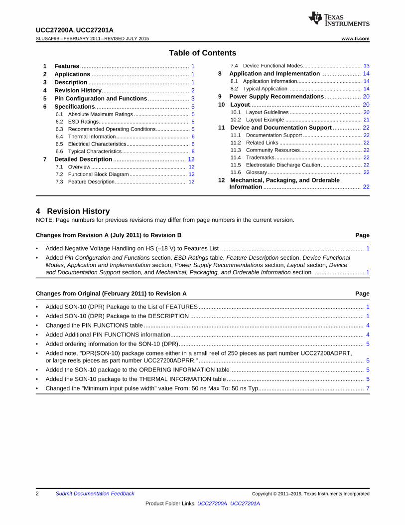
4 Revision HistoryNOTE: Page numbers for previous revisions may differ from page numbers in the current version.
Changes from Revision A (July 2011) to Revision B Page
• Added Negative Voltage Handling on HS (–18 V) to Features List ...................................................................................... 1• Added Pin Configuration and Functions section, ESD Ratings table, Feature Description section, Device Functional
Modes, Application and Implementation section, Power Supply Recommendations section, Layout section, Deviceand Documentation Support section, and Mechanical, Packaging, and Orderable Information section .............................. 1
Changes from Original (February 2011) to Revision A Page
• Added SON-10 (DPR) Package to the List of FEATURES .................................................................................................... 1• Added SON-10 (DPR) Package to the DESCRIPTION ......................................................................................................... 1• Changed the PIN FUNCTIONS table ..................................................................................................................................... 4• Added Additional PIN FUNCTIONS information..................................................................................................................... 4• Added ordering information for the SON-10 (DPR)................................................................................................................ 5• Added note, "DPR(SON-10) package comes either in a small reel of 250 pieces as part number UCC27200ADPRT,
or large reels pieces as part number UCC27200ADPRR." .................................................................................................... 5• Added the SON-10 package to the ORDERING INFORMATION table................................................................................. 5• Added the SON-10 package to the THERMAL INFORMATION table ................................................................................... 5• Changed the "Minimum input pulse width" value From: 50 ns Max To: 50 ns Typ................................................................ 7
UCC27200A, UCC27201ASLUSAF9B –FEBRUARY 2011–REVISED JULY 2015 www.ti.com
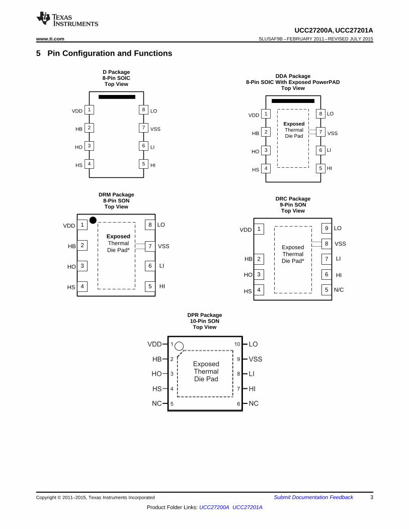
Pin FunctionsPIN
I/O DESCRIPTIONNAME DRM/D/DDA DRC DPR
Positive supply to the lower gate driver. De-couple this pin toVDD 1 1 1 I VSS (GND). Typical decoupling capacitor range is 0.22 μF to
1.0 μF.High-side bootstrap supply. The bootstrap diode is on-chip butthe external bootstrap capacitor is required. Connect positive
HB 2 2 2 I side of the bootstrap capacitor to this pin. Typical range of HBbypass capacitor is 0.022 μF to 0.1 μF, the value is dependanton the gate charge of the high-side MOSFET however.High-side output. Connect to the gate of the high-side powerHO 3 3 3 O MOSFET.High-side source connection. Connect to source of high-side
HS 4 4 4 I power MOSFET. Connect negative side of bootstrap capacitor tothis pin.
HI 5 6 7 I High-side input.LI 6 7 8 I Low-side input.
Negative supply terminal for the device which is generallyVSS 7 8 9 O grounded.Low-side output. Connect to the gate of the low-side powerLO 8 9 10 O MOSFET.
N/C — 5 5/6 — No connection. Pins labeled N/C have no connection.Connect to a large thermal mass trace or GND plane toPowerPAD (1) — — — — dramatically improve thermal performance.
(1) Pin VSS and the exposed thermal die pad are internally connected on the DDA and DRM packages only. Electrically referenced to VSS(GND).
VHB + 0.3,Output voltage on HO, VHO VRepetitive pulse <100 ns (3) VHS – 2 (VHB - VHS
<20)DC –1 120
Voltage on HS, VHS VRepetitive pulse <100 ns (3) –18 120
Voltage on HB, VHB –0.3 120 VVoltage On HB-HS –0.3 120 VOperating virtual junction temperature range, TJ –40 150 °CLead temperature (soldering, 10 sec.) 300 °CPower dissipation at TA = 25°C (D package) (4) 1.3 WPower dissipation at TA = 25°C (DDA package) (4) 2.7 WPower dissipation at TA = 25°C (DRM package) (4) 3.3 WPower dissipation at TA = 25°C (DRC package) (4) 2.86 WStorage temperature, Tstg –65 150 °C
(1) Stresses beyond those listed under Absolute Maximum Ratings may cause permanent damage to the device. These are stress ratingsonly, which do not imply functional operation of the device at these or any other conditions beyond those indicated under RecommendedOperating Conditions. Exposure to absolute-maximum-rated conditions for extended periods may affect device reliability.
(2) All voltages are with respect to Vss. Currents are positive into, negative out of the specified terminal.(3) Values are verified by characterization and are not production tested.(4) This data was taken using the JEDEC proposed high-K test PCB. See the THERMAL CHARACTERISTICS section for details.
6.2 ESD RatingsVALUE UNIT
Human body model (HBM), per ANSI/ESDA/JEDEC JS-001 (1) 2000V(ESD) Electrostatic discharge V
Charged-device model (CDM), per JEDEC specification JESD22-C101 (2) 1000
(1) JEDEC document JEP155 states that 500-V HBM allows safe manufacturing with a standard ESD control process.(2) JEDEC document JEP157 states that 250-V CDM allows safe manufacturing with a standard ESD control process.
6.3 Recommended Operating Conditionsover operating free-air temperature range (unless otherwise noted)
PARAMETER MIN NOM MAX UNITVDD Supply voltage 8 12 17 VVHS Voltage on HS –1 105 V
Voltage on HS, (repetitive pulse <100 ns) –15 110 VVHB VHS + 8, VHS + 17,Voltage on HB VVDD –1 115
Voltage slew rate on HS 50 V / nsTJ Operating junction temperature range –40 140 °C
tDLFF VLI falling to VLO falling nsTJ = -40 to 140°C CLOAD = 0 20 50TJ = -40 to 125°C CLOAD = 0 20 45
tDHFF VHI falling to VHO falling nsTJ = -40 to 140°C CLOAD = 0 20 50TJ = -40 to 125°C CLOAD = 0 20 45
tDLRR VLI rising to VLO rising nsTJ = -40 to 140°C CLOAD = 0 20 50TJ = -40 to 125°C CLOAD = 0 20 45
tDHRR VHI rising to VHO rising nsTJ = -40 to 140°C CLOAD = 0 20 50
DELAY MATCHINGtMON LI ON, HI OFF 1 7 nstMOFF LI OFF, HI ON 1 7 nsOUTPUT RISE AND FALL TIMEtR LO, HO CLOAD = 1000 pF 8 nstF LO, HO CLOAD = 1000 pF 7 nstR LO, HO (3 V to 9 V) CLOAD = 0.1 μF 0.35 0.6 ustF LO, HO (3 V to 9 V) CLOAD = 0.1 μF 0.3 0.6 usMISCELLANEOUS
Minimum input pulse width that changes the output 50 nsBootstrap diode turnoff time IF = 20 mA, IREV = 0.5 A (1) (2) 20 ns
(1) Typical values for TA = 25°C(2) IF: Forward current applied to bootstrap diode, IREV: Reverse current applied to bootstrap diode.
UCC27200A, UCC27201ASLUSAF9B –FEBRUARY 2011–REVISED JULY 2015 www.ti.com
7 Detailed Description
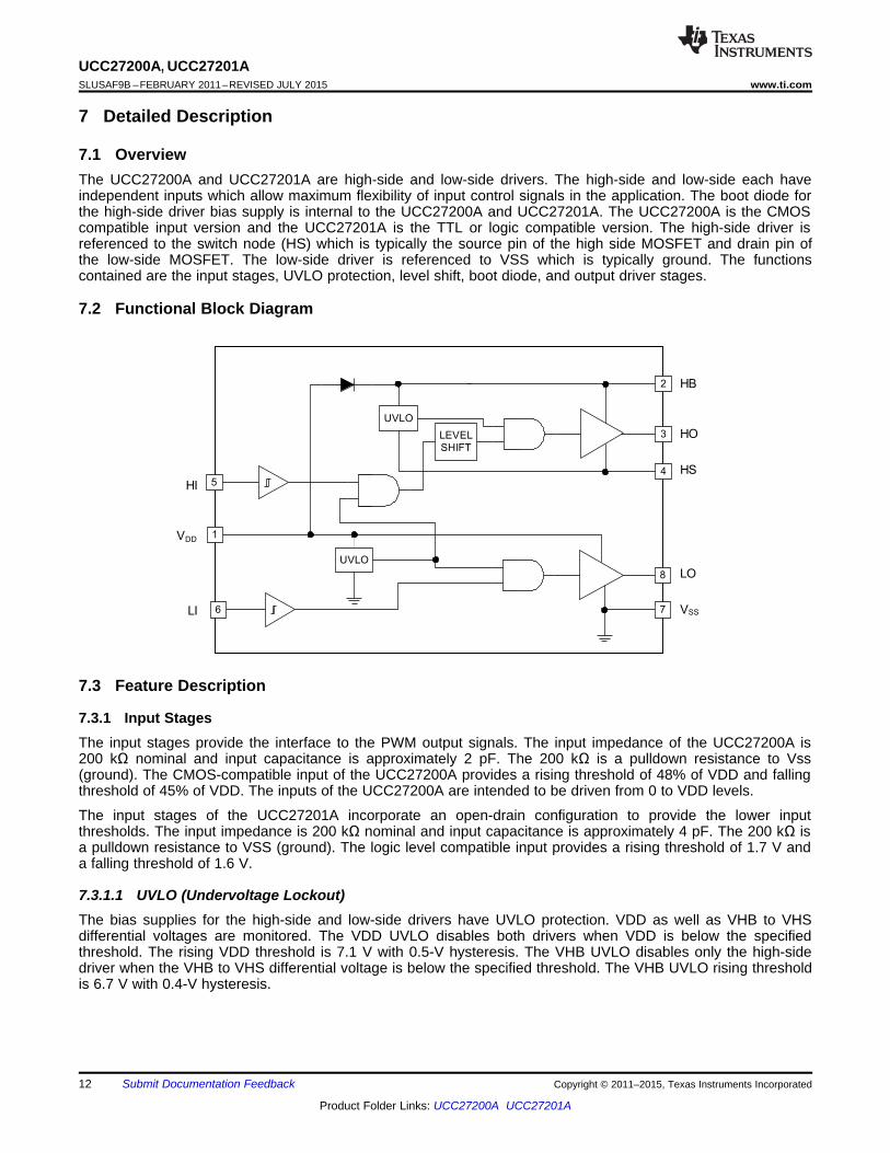
7.1 OverviewThe UCC27200A and UCC27201A are high-side and low-side drivers. The high-side and low-side each haveindependent inputs which allow maximum flexibility of input control signals in the application. The boot diode forthe high-side driver bias supply is internal to the UCC27200A and UCC27201A. The UCC27200A is the CMOScompatible input version and the UCC27201A is the TTL or logic compatible version. The high-side driver isreferenced to the switch node (HS) which is typically the source pin of the high side MOSFET and drain pin ofthe low-side MOSFET. The low-side driver is referenced to VSS which is typically ground. The functionscontained are the input stages, UVLO protection, level shift, boot diode, and output driver stages.
7.2 Functional Block Diagram
7.3 Feature Description
7.3.1 Input StagesThe input stages provide the interface to the PWM output signals. The input impedance of the UCC27200A is200 kΩ nominal and input capacitance is approximately 2 pF. The 200 kΩ is a pulldown resistance to Vss(ground). The CMOS-compatible input of the UCC27200A provides a rising threshold of 48% of VDD and fallingthreshold of 45% of VDD. The inputs of the UCC27200A are intended to be driven from 0 to VDD levels.
The input stages of the UCC27201A incorporate an open-drain configuration to provide the lower inputthresholds. The input impedance is 200 kΩ nominal and input capacitance is approximately 4 pF. The 200 kΩ isa pulldown resistance to VSS (ground). The logic level compatible input provides a rising threshold of 1.7 V anda falling threshold of 1.6 V.
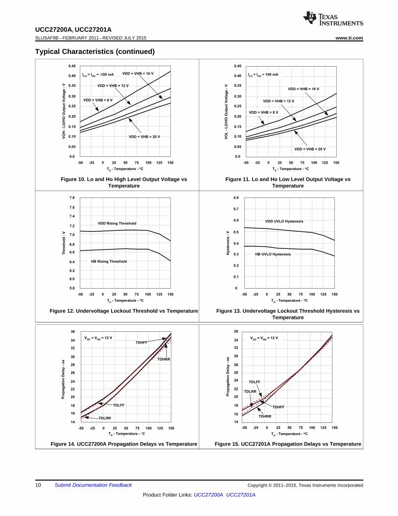
7.3.1.1 UVLO (Undervoltage Lockout)The bias supplies for the high-side and low-side drivers have UVLO protection. VDD as well as VHB to VHSdifferential voltages are monitored. The VDD UVLO disables both drivers when VDD is below the specifiedthreshold. The rising VDD threshold is 7.1 V with 0.5-V hysteresis. The VHB UVLO disables only the high-sidedriver when the VHB to VHS differential voltage is below the specified threshold. The VHB UVLO rising thresholdis 6.7 V with 0.4-V hysteresis.
UCC27200A, UCC27201Awww.ti.com SLUSAF9B –FEBRUARY 2011–REVISED JULY 2015
Feature Description (continued)7.3.1.2 Level ShiftThe level shift circuit is the interface from the high-side input to the high-side driver stage which is referenced tothe switch node (HS). The level shift allows control of the HO output referenced to the HS pin and providesexcellent delay matching with the low-side driver.
7.3.1.3 Boot DiodeThe boot diode necessary to generate the high-side bias is included in the UCC2720x family of drivers. Thediode anode is connected to VDD and cathode connected to VHB. With the VHB capacitor connected to HB andthe HS pins, the VHB capacitor charge is refreshed every switching cycle when HS transitions to ground. Theboot diode provides fast recovery times, low diode resistance, and voltage rating margin to allow for efficient andreliable operation.
7.3.1.4 Output StagesThe output stages are the interface to the power MOSFETs in the power train. High slew rate, low resistance,and high peak current capability of both output drivers allow for efficient switching of the power MOSFETs. Thelow-side output stage is referenced from VDD to VSS and the high-side is referenced from VHB to VHS.
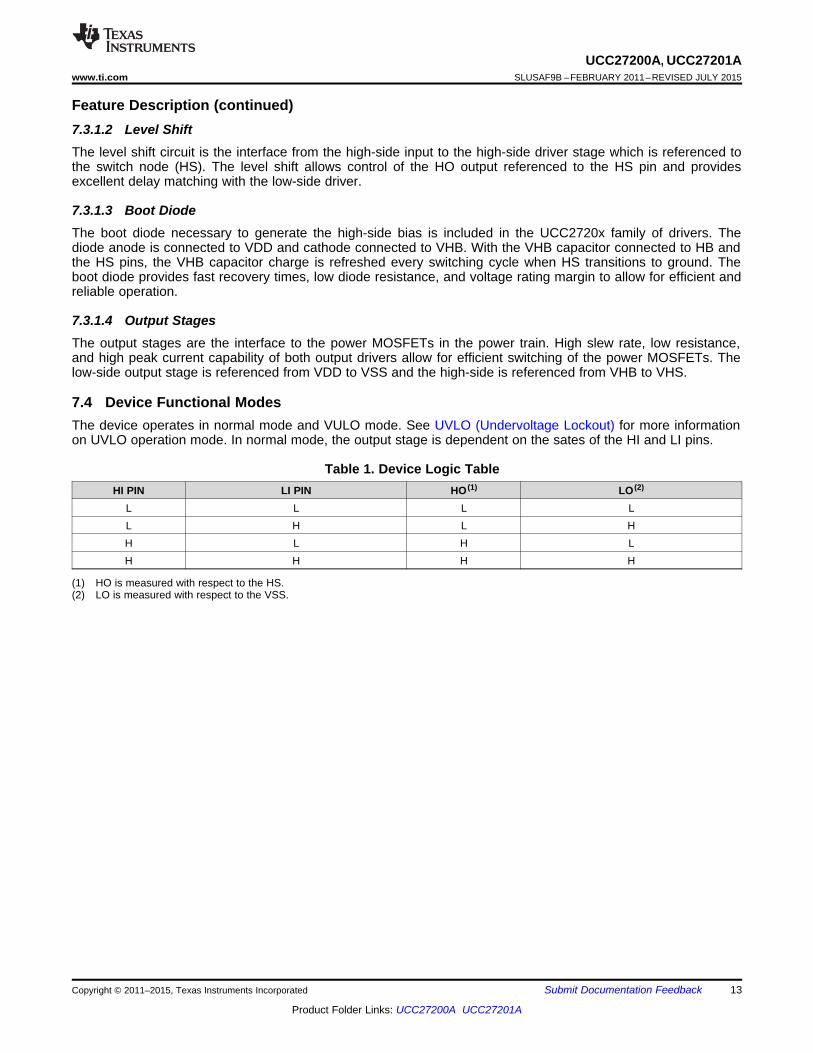
7.4 Device Functional ModesThe device operates in normal mode and VULO mode. See UVLO (Undervoltage Lockout) for more informationon UVLO operation mode. In normal mode, the output stage is dependent on the sates of the HI and LI pins.
Table 1. Device Logic TableHI PIN LI PIN HO (1) LO (2)
L L L LL H L HH L H LH H H H
(1) HO is measured with respect to the HS.(2) LO is measured with respect to the VSS.
UCC27200A, UCC27201ASLUSAF9B –FEBRUARY 2011–REVISED JULY 2015 www.ti.com
8 Application and Implementation
NOTEInformation in the following applications sections is not part of the TI componentspecification, and TI does not warrant its accuracy or completeness. TI’s customers areresponsible for determining suitability of components for their purposes. Customers shouldvalidate and test their design implementation to confirm system functionality.
8.1 Application InformationTo effect fast switching of power devices and reduce associated switching power losses, a powerful gate driver isemployed between the PWM output of controllers and the gates of the power semiconductor devices. Also, gatedrivers are indispensable when it is impossible for the PWM controller to directly drive the gates of the switchingdevices. With the advent of digital power, this situation will be often encountered because the PWM signal fromthe digital controller is often a 3.3-V logic signal which cannot effectively turn on a power switch. Level shiftingcircuitry is needed to boost the 3.3-V signal to the gate-drive voltage (such as 12 V) in order to fully turn on thepower device and minimize conduction losses. Traditional buffer drive circuits based on NPN/PNP bipolartransistors in totem-pole arrangement, being emitter follower configurations, prove inadequate with digital powerbecause they lack level-shifting capability. Gate drivers effectively combine both the level-shifting and buffer-drivefunctions. Gate drivers also find other needs such as minimizing the effect of high-frequency switching noise bylocating the high-current driver physically close to the power switch, driving gate-drive transformers andcontrolling floating power-device gates, reducing power dissipation and thermal stress in controllers by movinggate charge power losses from the controller into the driver.
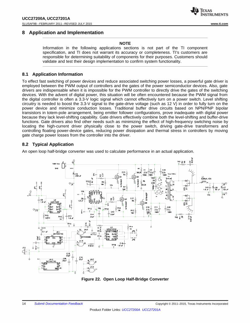
8.2 Typical ApplicationAn open loop half-bridge converter was used to calculate performance in an actual application.
UCC27201A Design RequirementsDESIGN PARAMETER EXAMPLE VALUE
Supply Voltage, VDD 12 VVoltage on HS, VHS 0 V to 100 VVoltage on HB, VHB 12 V to 112 VOutput 4 V, 20 AFrequency 200 kHz
8.2.2 Detailed Design Procedure
8.2.2.1 Switching the MOSFETsAchieving optimum drive performance at high frequency efficiently requires special attention to layout andminimizing parasitic inductances. Take care at the driver die and package level as well as the PCB layout toreduce parasitic inductances as much as possible. Figure 23 shows the main parasitic inductance elements andcurrent flow paths during the turnon and turnoff of the MOSFET by charging and discharging its CGScapacitance.
Figure 23. MOSFET Drive Paths and Circuit Parasitics
UCC27200A, UCC27201ASLUSAF9B –FEBRUARY 2011–REVISED JULY 2015 www.ti.com
The ISOURCE current charges the CGS gate capacitor and the ISINK current discharges it. The rise and fall time ofthe voltage across the gate to source defines how quickly the MOSFET can be switched. Based on actualmeasurements, the analytical curves in Figure 24 and Figure 25 indicate the output voltage and current of thedrivers during the discharge of the load capacitor. Figure 24 shows voltage and current as a function of time.Figure 25 indicates the relationship of voltage and current during fast switching. These figures demonstrate theactual switching process and limitations due to parasitic inductances.
Figure 25. Turnoff Voltage and Current Switching DiagramFigure 24. Turnoff Voltage and Current vs Time
Turning off the MOSFET needs to be achieved as fast as possible to minimize switching losses. For this reasonthe UCC2720x drivers are designed for high peak currents and low output resistance. The sink capability isspecified as 0.18 V at 100-mA dc current implying 1.8-Ω RDS(on). With 12-V drive voltage, no parasitic inductanceand a linear resistance, one would expect initial sink current amplitude of 6.7 A for both high-side and low-sidedrivers. Assuming a pure R-C discharge circuit of the gate capacitor, one would expect the voltage and currentwaveforms to be exponential. Due to the parasitic inductances and non-linear resistance of the driverMOSFET’S, the actual waveforms have some ringing and the peak-sink current of the drivers is approximately3.3 A as shown in Figure 19. The overall parasitic inductance of the drive circuit is estimated at 4 nH. Theinternal parasitic inductance of the SOIC-8 package is estimated to be 2 nH including bond wires and leads. TheSON-8 package reduces the internal parasitic inductances by more than 50%.
UCC27200A, UCC27201Awww.ti.com SLUSAF9B –FEBRUARY 2011–REVISED JULY 2015
Actual measured waveforms are shown in Figure 26 and Figure 27. As shown, the typical rise time of 8 ns andfall time of 7 ns is conservatively rated.
Figure 26. VLO and VHO Rise Time, 1-nf Load, 5 ns/div Figure 27. VLO and VHO Fall Time, 1-nf Load, 5-ns/div
8.2.2.2 Dynamic Switching of the MOSFETsThe true behavior of MOSFETS presents a dynamic capacitive load primarily at the gate to source thresholdvoltage. Using the turnoff case as the example, when the gate to source threshold voltage is reached the drainvoltage starts rising, the drain to gate parasitic capacitance couples charge into the gate resulting in the turn offplateau. The relatively low threshold voltages of many MOSFETS and the increased charge that has to beremoved (Miller charge) makes good driver performance necessary for efficient switching. An open-loop, half-bridge power converter was utilized to evaluate performance in actual applications. The schematic of the half-bridge converter is shown in . The turn off waveforms of the UCC27200A driving two MOSFETs in parallel isshown in Figure 28 and Figure 29.
Figure 29. VHO Fall Time in Half-Bridge ConverterFigure 28. VLO Fall Time in Half-Bridge Converter
UCC27200A, UCC27201ASLUSAF9B –FEBRUARY 2011–REVISED JULY 2015 www.ti.com
8.2.2.3 Delay Matching and Narrow Pulse WidthsThe total delays encountered in the PWM, driver and power stage need to be considered for a number ofreasons, primarily delay in current limit response. Also to be considered are differences in delays between thedrivers which can lead to various concerns depending on the topology. The sync-buck topology switchingrequires careful selection of dead-time between the high- and low-side switches to avoid 1) cross conduction and2) excessive body diode conduction. Bridge topologies can be affected by a resulting volt-sec imbalance on thetransformer if there is imbalance in the high and low side pulse widths in a steady-state condition.
Narrow pulse width performance is an important consideration when transient and short circuit conditions areencountered. Although there may be relatively long steady state PWM output-driver-MOSFET signals, verynarrow pulses may be encountered in 1) soft start, 2) large load transients, and 3) short circuit conditions.
The UCC2720x driver family offers excellent performance regarding high and low-side driver delay matching andnarrow pulse width performance. The delay matching waveforms are shown in Figure 30 and Figure 31. TheUCC2720x driver narrow pulse performance is shown in Figure 32 and Figure 33.
Figure 30. VLO and VHO Rising Edge Delay Matching Figure 31. VLO and VHO Falling Edge Delay Matching
UCC27200A, UCC27201Awww.ti.com SLUSAF9B –FEBRUARY 2011–REVISED JULY 2015
8.2.2.4 Boot Diode PerformanceThe UCC2720x family of drivers incorporates the bootstrap diode necessary to generate the high-side biasinternally. The characteristics of this diode are important to achieve efficient, reliable operation. The dccharacteristics to consider are VF and dynamic resistance. A low VF and high dynamic resistance results in ahigh forward voltage during charging of the bootstrap capacitor. The UCC2720x has a boot diode rated at 0.65-VVF and dynamic resistance of 0.6 Ω for reliable charge transfer to the bootstrap capacitor. The dynamiccharacteristics to consider are diode recovery time and stored charge. Diode recovery times that are specifiedwith no conditions can be misleading. Diode recovery times at no forward current (IF) can be noticeably less thanwith forward current applied. The UCC2720x boot diode recovery is specified at 20ns at IF = 20 mA, IREV = 0.5 A.At 0 mA IF the reverse recovery time is 15 ns.
Another less obvious consideration is how the stored charge of the diode is affected by applied voltage. On everyswitching transition when the HS node transitions from low to high, charge is removed from the boot capacitor tocharge the capacitance of the reverse biased diode. This is a portion of the driver power losses and reduces thevoltage on the HB capacitor. At higher applied voltages, the stored charge of the UCC2720x PN diode is oftenless than a comparable Schottky diode.
8.2.3 Application Curves
Figure 35. VHO Fall Time in Half-Bridge ConverterFigure 34. VLO Fall Time in Half-Bridge Converter
UCC27200A, UCC27201ASLUSAF9B –FEBRUARY 2011–REVISED JULY 2015 www.ti.com
9 Power Supply RecommendationsThe bias supply voltage range for which the device is rated to operate is from 8 V to 17 V. The lower end of thisrange is governed by the internal undervoltage-lockout (UVLO) protection feature on the VDD pin supply circuitblocks. Whenever the driver is in UVLO condition when the VDD pin voltage is below the V(ON) supply startthreshold, this feature holds the output low, regardless of the status of the inputs. The upper end of this range isdriven by the 20-V absolute maximum voltage rating of the VDD pin of the device (which is a stress rating).Keeping a 3-V margin to allow for transient voltage spikes, the maximum recommended voltage for the VDD pinis 17 V. The UVLO protection feature also involves a hysteresis function. This means that when the VDD pin biasvoltage has exceeded the threshold voltage and device begins to operate, and if the voltage drops, then thedevice continues to deliver normal functionality unless the voltage drop exceeds the hysteresis specificationVDD(hys).Therefore, ensuring that, while operating at or near the 8-V range, the voltage ripple on the auxiliarypower supply output is smaller than the hysteresis specification of the device is important to avoid triggeringdevice shutdown. During system shutdown, the device operation continues until the VDD pin voltage hasdropped below the V(OFF) threshold which must be accounted for while evaluating system shutdown timingdesign requirements. Likewise, at system startup, the device does not begin operation until the VDD pin voltagehas exceeded above the V(ON) threshold. The quiescent current consumed by the internal circuit blocks of thedevice is supplied through the VDD pin. Although this fact is well known, recognizing that the charge for sourcecurrent pulses delivered by the HO pin is also supplied through the same VDD pin is important. As a result, everytime a current is sourced out of the HO pin a corresponding current pulse is delivered into the device through theVDD pin. Thus ensuring that a local bypass capacitor is provided between the VDD and GND pins and locatedas close to the device as possible for the purpose of decoupling is important. A low ESR, ceramic surface mountcapacitor is a must. TI recommends using a capacitor in the range 0.22 uF to 4.7 uF between VDD and GND. Ina similar manner, the current pulses delivered by the LO pin are sourced from the HB pin. Therefore a 0.022-uFto 0.1-uF local decoupling capacitor is recommended between the HB and HS pins.
10 Layout
10.1 Layout GuidelinesTo improve the switching characteristics and efficiency of a design, the following layout rules should be followed.• Locate the driver as close as possible to the MOSFETs.• Locate the VDD and VHB (bootstrap) capacitors as close as possible to the driver.• Pay close attention to the GND trace. Use the thermal pad of the DDA and DRM package as GND by
connecting it to the VSS pin (GND). The GND trace from the driver goes directly to the source of theMOSFET but should not be in the high current path of the MOSFET(S) drain or source current.
• Use similar rules for the HS node as for GND for the high side driver.• Use wide traces for LO and HO closely following the associated GND or HS traces. 60 mil to 100 mil width is
preferable where possible.• Use as least two or more vias if the driver outputs or SW node needs to be routed from one layer to another.
For GND the number of vias needs to be a consideration of the thermal pad requirements as well as parasiticinductance.
• Avoid LI and HI (driver input) going close to the HS node or any other high dV/dT traces that can inducesignificant noise into the relatively high impedance leads.
• Keep in mind that a poor layout can cause a significant drop in efficiency versus a good PCB layout and caneven lead to decreased reliability of the whole system.
These references and links to additional information may be found at www.ti.com.1. Additional layout guidelines for PCB land patterns may be found in Application Brief SLUA2712. Additional thermal performance guidelines may be found in Application Reports SLMA002 and SLMA004
UCC27200A, UCC27201ASLUSAF9B –FEBRUARY 2011–REVISED JULY 2015 www.ti.com
11 Device and Documentation Support
11.1 Documentation Support
11.1.1 Related DocumentationFor related documentation see the following:• QFN/SON PCB Attachment, SLUA271• PowerPAD Thermally Enhanced Package, SLMA002• PowerPAD Made Easy, SLMA004
11.2 Related LinksThe table below lists quick access links. Categories include technical documents, support and communityresources, tools and software, and quick access to sample or buy.
Table 2. Related LinksTECHNICAL TOOLS & SUPPORT &PARTS PRODUCT FOLDER SAMPLE & BUY DOCUMENTS SOFTWARE COMMUNITY
UCC27200A Click here Click here Click here Click here Click hereUCC27201A Click here Click here Click here Click here Click here
11.3 Community ResourcesThe following links connect to TI community resources. Linked contents are provided "AS IS" by the respectivecontributors. They do not constitute TI specifications and do not necessarily reflect TI's views; see TI's Terms ofUse.
TI E2E™ Online Community TI's Engineer-to-Engineer (E2E) Community. Created to foster collaborationamong engineers. At e2e.ti.com, you can ask questions, share knowledge, explore ideas and helpsolve problems with fellow engineers.
Design Support TI's Design Support Quickly find helpful E2E forums along with design support tools andcontact information for technical support.
11.4 TrademarksPowerPAD, E2E are trademarks of Texas Instruments.All other trademarks are the property of their respective owners.
11.5 Electrostatic Discharge CautionThese devices have limited built-in ESD protection. The leads should be shorted together or the device placed in conductive foamduring storage or handling to prevent electrostatic damage to the MOS gates.
11.6 GlossarySLYZ022 — TI Glossary.
This glossary lists and explains terms, acronyms, and definitions.
12 Mechanical, Packaging, and Orderable InformationThe following pages include mechanical, packaging, and orderable information. This information is the mostcurrent data available for the designated devices. This data is subject to change without notice and revision ofthis document. For browser-based versions of this data sheet, refer to the left-hand navigation.
UCC27201ADRMT ACTIVE VSON DRM 8 250 Green (RoHS& no Sb/Br)
CU NIPDAUAG | Call TI Level-1-260C-UNLIM -40 to 140 27201A
(1) The marketing status values are defined as follows:ACTIVE: Product device recommended for new designs.LIFEBUY: TI has announced that the device will be discontinued, and a lifetime-buy period is in effect.NRND: Not recommended for new designs. Device is in production to support existing customers, but TI does not recommend using this part in a new design.PREVIEW: Device has been announced but is not in production. Samples may or may not be available.OBSOLETE: TI has discontinued the production of the device.
(2) RoHS: TI defines "RoHS" to mean semiconductor products that are compliant with the current EU RoHS requirements for all 10 RoHS substances, including the requirement that RoHS substancedo not exceed 0.1% by weight in homogeneous materials. Where designed to be soldered at high temperatures, "RoHS" products are suitable for use in specified lead-free processes. TI mayreference these types of products as "Pb-Free".RoHS Exempt: TI defines "RoHS Exempt" to mean products that contain lead but are compliant with EU RoHS pursuant to a specific EU RoHS exemption.Green: TI defines "Green" to mean the content of Chlorine (Cl) and Bromine (Br) based flame retardants meet JS709B low halogen requirements of <=1000ppm threshold. Antimony trioxide basedflame retardants must also meet the <=1000ppm threshold requirement.
(3) MSL, Peak Temp. - The Moisture Sensitivity Level rating according to the JEDEC industry standard classifications, and peak solder temperature.
(4) There may be additional marking, which relates to the logo, the lot trace code information, or the environmental category on the device.
(5) Multiple Device Markings will be inside parentheses. Only one Device Marking contained in parentheses and separated by a "~" will appear on a device. If a line is indented then it is a continuationof the previous line and the two combined represent the entire Device Marking for that device.
(6) Lead/Ball Finish - Orderable Devices may have multiple material finish options. Finish options are separated by a vertical ruled line. Lead/Ball Finish values may wrap to two lines if the finishvalue exceeds the maximum column width.
Important Information and Disclaimer:The information provided on this page represents TI's knowledge and belief as of the date that it is provided. TI bases its knowledge and belief on informationprovided by third parties, and makes no representation or warranty as to the accuracy of such information. Efforts are underway to better integrate information from third parties. TI has taken andcontinues to take reasonable steps to provide representative and accurate information but may not have conducted destructive testing or chemical analysis on incoming materials and chemicals.TI and TI suppliers consider certain information to be proprietary, and thus CAS numbers and other limited information may not be available for release.
In no event shall TI's liability arising out of such information exceed the total purchase price of the TI part(s) at issue in this document sold by TI to Customer on an annual basis.
Texas Instruments Incorporated (TI) reserves the right to make corrections, enhancements, improvements and other changes to itssemiconductor products and services per JESD46, latest issue, and to discontinue any product or service per JESD48, latest issue. Buyersshould obtain the latest relevant information before placing orders and should verify that such information is current and complete.TI’s published terms of sale for semiconductor products (http://www.ti.com/sc/docs/stdterms.htm) apply to the sale of packaged integratedcircuit products that TI has qualified and released to market. Additional terms may apply to the use or sale of other types of TI products andservices.Reproduction of significant portions of TI information in TI data sheets is permissible only if reproduction is without alteration and isaccompanied by all associated warranties, conditions, limitations, and notices. TI is not responsible or liable for such reproduceddocumentation. Information of third parties may be subject to additional restrictions. Resale of TI products or services with statementsdifferent from or beyond the parameters stated by TI for that product or service voids all express and any implied warranties for theassociated TI product or service and is an unfair and deceptive business practice. TI is not responsible or liable for any such statements.Buyers and others who are developing systems that incorporate TI products (collectively, “Designers”) understand and agree that Designersremain responsible for using their independent analysis, evaluation and judgment in designing their applications and that Designers havefull and exclusive responsibility to assure the safety of Designers' applications and compliance of their applications (and of all TI productsused in or for Designers’ applications) with all applicable regulations, laws and other applicable requirements. Designer represents that, withrespect to their applications, Designer has all the necessary expertise to create and implement safeguards that (1) anticipate dangerousconsequences of failures, (2) monitor failures and their consequences, and (3) lessen the likelihood of failures that might cause harm andtake appropriate actions. Designer agrees that prior to using or distributing any applications that include TI products, Designer willthoroughly test such applications and the functionality of such TI products as used in such applications.TI’s provision of technical, application or other design advice, quality characterization, reliability data or other services or information,including, but not limited to, reference designs and materials relating to evaluation modules, (collectively, “TI Resources”) are intended toassist designers who are developing applications that incorporate TI products; by downloading, accessing or using TI Resources in anyway, Designer (individually or, if Designer is acting on behalf of a company, Designer’s company) agrees to use any particular TI Resourcesolely for this purpose and subject to the terms of this Notice.TI’s provision of TI Resources does not expand or otherwise alter TI’s applicable published warranties or warranty disclaimers for TIproducts, and no additional obligations or liabilities arise from TI providing such TI Resources. TI reserves the right to make corrections,enhancements, improvements and other changes to its TI Resources. TI has not conducted any testing other than that specificallydescribed in the published documentation for a particular TI Resource.Designer is authorized to use, copy and modify any individual TI Resource only in connection with the development of applications thatinclude the TI product(s) identified in such TI Resource. NO OTHER LICENSE, EXPRESS OR IMPLIED, BY ESTOPPEL OR OTHERWISETO ANY OTHER TI INTELLECTUAL PROPERTY RIGHT, AND NO LICENSE TO ANY TECHNOLOGY OR INTELLECTUAL PROPERTYRIGHT OF TI OR ANY THIRD PARTY IS GRANTED HEREIN, including but not limited to any patent right, copyright, mask work right, orother intellectual property right relating to any combination, machine, or process in which TI products or services are used. Informationregarding or referencing third-party products or services does not constitute a license to use such products or services, or a warranty orendorsement thereof. Use of TI Resources may require a license from a third party under the patents or other intellectual property of thethird party, or a license from TI under the patents or other intellectual property of TI.TI RESOURCES ARE PROVIDED “AS IS” AND WITH ALL FAULTS. TI DISCLAIMS ALL OTHER WARRANTIES ORREPRESENTATIONS, EXPRESS OR IMPLIED, REGARDING RESOURCES OR USE THEREOF, INCLUDING BUT NOT LIMITED TOACCURACY OR COMPLETENESS, TITLE, ANY EPIDEMIC FAILURE WARRANTY AND ANY IMPLIED WARRANTIES OFMERCHANTABILITY, FITNESS FOR A PARTICULAR PURPOSE, AND NON-INFRINGEMENT OF ANY THIRD PARTY INTELLECTUALPROPERTY RIGHTS. TI SHALL NOT BE LIABLE FOR AND SHALL NOT DEFEND OR INDEMNIFY DESIGNER AGAINST ANY CLAIM,INCLUDING BUT NOT LIMITED TO ANY INFRINGEMENT CLAIM THAT RELATES TO OR IS BASED ON ANY COMBINATION OFPRODUCTS EVEN IF DESCRIBED IN TI RESOURCES OR OTHERWISE. IN NO EVENT SHALL TI BE LIABLE FOR ANY ACTUAL,DIRECT, SPECIAL, COLLATERAL, INDIRECT, PUNITIVE, INCIDENTAL, CONSEQUENTIAL OR EXEMPLARY DAMAGES INCONNECTION WITH OR ARISING OUT OF TI RESOURCES OR USE THEREOF, AND REGARDLESS OF WHETHER TI HAS BEENADVISED OF THE POSSIBILITY OF SUCH DAMAGES.Unless TI has explicitly designated an individual product as meeting the requirements of a particular industry standard (e.g., ISO/TS 16949and ISO 26262), TI is not responsible for any failure to meet such industry standard requirements.Where TI specifically promotes products as facilitating functional safety or as compliant with industry functional safety standards, suchproducts are intended to help enable customers to design and create their own applications that meet applicable functional safety standardsand requirements. Using products in an application does not by itself establish any safety features in the application. Designers mustensure compliance with safety-related requirements and standards applicable to their applications. Designer may not use any TI products inlife-critical medical equipment unless authorized officers of the parties have executed a special contract specifically governing such use.Life-critical medical equipment is medical equipment where failure of such equipment would cause serious bodily injury or death (e.g., lifesupport, pacemakers, defibrillators, heart pumps, neurostimulators, and implantables). Such equipment includes, without limitation, allmedical devices identified by the U.S. Food and Drug Administration as Class III devices and equivalent classifications outside the U.S.TI may expressly designate certain products as completing a particular qualification (e.g., Q100, Military Grade, or Enhanced Product).Designers agree that it has the necessary expertise to select the product with the appropriate qualification designation for their applicationsand that proper product selection is at Designers’ own risk. Designers are solely responsible for compliance with all legal and regulatoryrequirements in connection with such selection.Designer will fully indemnify TI and its representatives against any damages, costs, losses, and/or liabilities arising out of Designer’s non-compliance with the terms and provisions of this Notice.