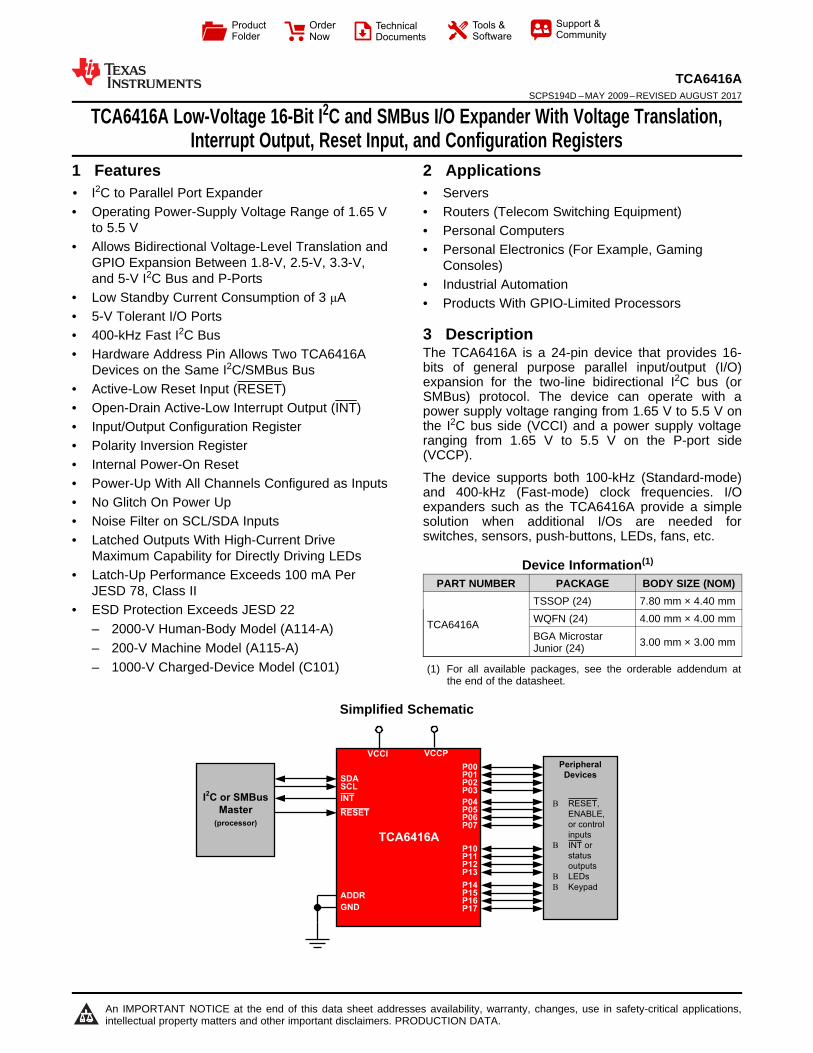
TCA6416A I 2 C or SMBus Master (processor) SDA SCL INT P10 P11 P12 P13 VCCI ADDR GND VCCP P14 P15 P16 P17 P00 P01 P02 P03 P04 P05 P06 P07 RESET Peripheral Devices B RESET, ENABLE, or control inputs B INT or status outputs B LEDs B Keypad Product Folder Order Now Technical Documents Tools & Software Support & Community An IMPORTANT NOTICE at the end of this data sheet addresses availability, warranty, changes, use in safety-critical applications, intellectual property matters and other important disclaimers. PRODUCTION DATA. TCA6416A SCPS194D – MAY 2009 – REVISED AUGUST 2017 TCA6416A Low-Voltage 16-Bit I 2 C and SMBus I/O Expander With Voltage Translation, Interrupt Output, Reset Input, and Configuration Registers 1 1 Features 1• I 2 C to Parallel Port Expander • Operating Power-Supply Voltage Range of 1.65 V to 5.5 V • Allows Bidirectional Voltage-Level Translation and GPIO Expansion Between 1.8-V, 2.5-V, 3.3-V, and 5-V I 2 C Bus and P-Ports • Low Standby Current Consumption of 3 μA • 5-V Tolerant I/O Ports • 400-kHz Fast I 2 C Bus • Hardware Address Pin Allows Two TCA6416A Devices on the Same I 2 C/SMBus Bus • Active-Low Reset Input (RESET) • Open-Drain Active-Low Interrupt Output (INT) • Input/Output Configuration Register • Polarity Inversion Register • Internal Power-On Reset • Power-Up With All Channels Configured as Inputs • No Glitch On Power Up • Noise Filter on SCL/SDA Inputs • Latched Outputs With High-Current Drive Maximum Capability for Directly Driving LEDs • Latch-Up Performance Exceeds 100 mA Per JESD 78, Class II • ESD Protection Exceeds JESD 22 – 2000-V Human-Body Model (A114-A) – 200-V Machine Model (A115-A) – 1000-V Charged-Device Model (C101) 2 Applications • Servers • Routers (Telecom Switching Equipment) • Personal Computers • Personal Electronics (For Example, Gaming Consoles) • Industrial Automation • Products With GPIO-Limited Processors 3 Description The TCA6416A is a 24-pin device that provides 16- bits of general purpose parallel input/output (I/O) expansion for the two-line bidirectional I 2 C bus (or SMBus) protocol. The device can operate with a power supply voltage ranging from 1.65 V to 5.5 V on the I 2 C bus side (VCCI) and a power supply voltage ranging from 1.65 V to 5.5 V on the P-port side (VCCP). The device supports both 100-kHz (Standard-mode) and 400-kHz (Fast-mode) clock frequencies. I/O expanders such as the TCA6416A provide a simple solution when additional I/Os are needed for switches, sensors, push-buttons, LEDs, fans, etc. Device Information (1) PART NUMBER PACKAGE BODY SIZE (NOM) TCA6416A TSSOP (24) 7.80 mm × 4.40 mm WQFN (24) 4.00 mm × 4.00 mm BGA Microstar Junior (24) 3.00 mm × 3.00 mm (1) For all available packages, see the orderable addendum at the end of the datasheet. Simplified Schematic
Transcript
TCA6416A
I2C or SMBus
Master
(processor)
SDASCL
INT
P10P11P12P13
VCCI
ADDR
GND
VCCP
P14P15P16P17
P00P01P02P03
P04P05P06P07
RESET
Peripheral
Devices
B RESET,
ENABLE,
or control
inputs
B INT or
status
outputs
B LEDs
B Keypad
Product
Folder
Order
Now
Technical
Documents
Tools &
Software
Support &Community
An IMPORTANT NOTICE at the end of this data sheet addresses availability, warranty, changes, use in safety-critical applications,intellectual property matters and other important disclaimers. PRODUCTION DATA.
TCA6416ASCPS194D –MAY 2009–REVISED AUGUST 2017
TCA6416A Low-Voltage 16-Bit I2C and SMBus I/O Expander With Voltage Translation,Interrupt Output, Reset Input, and Configuration Registers
1
1 Features1• I2C to Parallel Port Expander• Operating Power-Supply Voltage Range of 1.65 V
to 5.5 V• Allows Bidirectional Voltage-Level Translation and
GPIO Expansion Between 1.8-V, 2.5-V, 3.3-V,and 5-V I2C Bus and P-Ports
• Low Standby Current Consumption of 3 μA• 5-V Tolerant I/O Ports• 400-kHz Fast I2C Bus• Hardware Address Pin Allows Two TCA6416A
Devices on the Same I2C/SMBus Bus• Active-Low Reset Input (RESET)• Open-Drain Active-Low Interrupt Output (INT)• Input/Output Configuration Register• Polarity Inversion Register• Internal Power-On Reset• Power-Up With All Channels Configured as Inputs• No Glitch On Power Up• Noise Filter on SCL/SDA Inputs• Latched Outputs With High-Current Drive
Maximum Capability for Directly Driving LEDs• Latch-Up Performance Exceeds 100 mA Per
JESD 78, Class II• ESD Protection Exceeds JESD 22
– 2000-V Human-Body Model (A114-A)– 200-V Machine Model (A115-A)– 1000-V Charged-Device Model (C101)
2 Applications• Servers• Routers (Telecom Switching Equipment)• Personal Computers• Personal Electronics (For Example, Gaming
Consoles)• Industrial Automation• Products With GPIO-Limited Processors
3 DescriptionThe TCA6416A is a 24-pin device that provides 16-bits of general purpose parallel input/output (I/O)expansion for the two-line bidirectional I2C bus (orSMBus) protocol. The device can operate with apower supply voltage ranging from 1.65 V to 5.5 V onthe I2C bus side (VCCI) and a power supply voltageranging from 1.65 V to 5.5 V on the P-port side(VCCP).
The device supports both 100-kHz (Standard-mode)and 400-kHz (Fast-mode) clock frequencies. I/Oexpanders such as the TCA6416A provide a simplesolution when additional I/Os are needed forswitches, sensors, push-buttons, LEDs, fans, etc.
Device Information(1)
PART NUMBER PACKAGE BODY SIZE (NOM)
TCA6416A
TSSOP (24) 7.80 mm × 4.40 mmWQFN (24) 4.00 mm × 4.00 mmBGA MicrostarJunior (24) 3.00 mm × 3.00 mm
(1) For all available packages, see the orderable addendum atthe end of the datasheet.
12 Device and Documentation Support ................. 3312.1 Trademarks ........................................................... 3312.2 Electrostatic Discharge Caution............................ 3312.3 Glossary ................................................................ 33
13 Mechanical, Packaging, and OrderableInformation ........................................................... 33
4 Revision HistoryNOTE: Page numbers for previous revisions may differ from page numbers in the current version.
Changes from Revision C (September 2015) to Revision D Page
• Changed the tvd(data) MAX value From: 1 µs To: 0.9 µs in the I2C Interface Timing Requirements table............................... 8• Changed the tvd(ack) MAX value From: 1 µs To: 0.9 µs in the I2C Interface Timing Requirements table................................ 8
Changes from Revision B (January 2015) to Revision C Page
• Changed units for tIV and tIR parameters from ns to µs.......................................................................................................... 8
Changes from Revision A (November 2009) to Revision B Page
• Added ESD Ratings table, Feature Description section, Device Functional Modes, Application and Implementationsection, Power Supply Recommendations section, Layout section, Device and Documentation Support section, andMechanical, Packaging, and Orderable Information section. ................................................................................................ 1
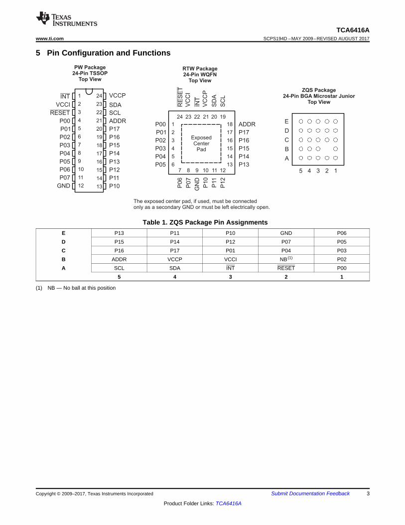
INT 1 22 A3 Interrupt output. Connect to VCCI or VCCP through a pull-up resistor.VCCI 2 23 B3 Supply voltage of I2C bus. Connect directly to the supply voltage of the external I2C master.
RESET 3 24 A2 Active-low reset input. Connect to VCCI or VCCP through a pull-up resistor, if no active connectionis used.
P00 4 1 A1 P-port input/output (push-pull design structure). At power on, P00 is configured as an input.P01 5 2 C3 P-port input/output (push-pull design structure). At power on, P01 is configured as an input.P02 6 3 B1 P-port input/output (push-pull design structure). At power on, P02 is configured as an input.P03 7 4 C1 P-port input/output (push-pull design structure). At power on, P03 is configured as an input.P04 8 5 C2 P-port input/output (push-pull design structure). At power on, P04 is configured as an input.P05 9 6 D1 P-port input/output (push-pull design structure). At power on, P05 is configured as an input.P06 10 7 E1 P-port input/output (push-pull design structure). At power on, P06 is configured as an input.P07 11 8 D2 P-port input/output (push-pull design structure). At power on, P07 is configured as an input.GND 12 9 E2 GroundP10 13 10 E3 P-port input/output (push-pull design structure). At power on, P10 is configured as an input.P11 14 11 E4 P-port input/output (push-pull design structure). At power on, P11 is configured as an input.P12 15 12 D3 P-port input/output (push-pull design structure). At power on, P12 is configured as an input.P13 16 13 E5 P-port input/output (push-pull design structure). At power on, P13 is configured as an input.P14 17 14 D4 P-port input/output (push-pull design structure). At power on, P14 is configured as an input.P15 18 15 D5 P-port input/output (push-pull design structure). At power on, P15 is configured as an input.P16 19 16 C5 P-port input/output (push-pull design structure). At power on, P16 is configured as an input.P17 20 17 C4 P-port input/output (push-pull design structure). At power on, P17 is configured as an input.ADDR 21 18 B5 Address input. Connect directly to VCCP or ground.SCL 22 19 A5 Serial clock bus. Connect to VCCI through a pull-up resistor.SDA 23 20 A4 Serial data bus. Connect to VCCI through a pull-up resistor.VCCP 24 21 B4 Supply voltage of TCA6416A for P-ports
(1) Stresses beyond those listed under Absolute Maximum Ratings may cause permanent damage to the device. These are stress ratingsonly, and functional operation of the device at these or any other conditions beyond those indicated under Recommended OperatingConditions is not implied. Exposure to absolute-maximum-rated conditions for extended periods may affect device reliability.
(2) The input negative-voltage and output voltage ratings may be exceeded if the input and output current ratings are observed.
6 Specifications
6.1 Absolute Maximum Ratings (1)
over operating free-air temperature range (unless otherwise noted)MIN MAX UNIT
VCCI Supply voltage –0.5 6.5 VVCCP Supply voltage –0.5 6.5 VVI Input voltage (2) –0.5 6.5 VVO Output voltage (2) –0.5 6.5 VIIK Input clamp current ADDR, RESET, SCL VI < 0 ±20 mAIOK Output clamp current INT VO < 0 ±20 mA
IIOK Input/output clamp currentP port VO < 0 or VO > VCCP ±20
mASDA VO < 0 or VO > VCCI ±20
IOL Continuous output low currentP port VO = 0 to VCCP 50
mASDA, INT VO = 0 to VCCI 25
IOH Continuous output high current P port VO = 0 to VCCP 50 mA
ICC
Continuous current through GND 200mAContinuous current through VCCP 160
Continuous current through VCCI 10Tstg Storage temperature –65 150 °C
(1) JEDEC document JEP155 states that 500-V HBM allows safe manufacturing with a standard ESD control process.(2) JEDEC document JEP157 states that 250-V CDM allows safe manufacturing with a standard ESD control process.
6.2 ESD RatingsVALUE UNIT
V(ESD) Electrostatic dischargeHuman-body model (HBM), per ANSI/ESDA/JEDEC JS-001 (1) ±2000
VCharged-device model (CDM), per JEDEC specification JESD22-C101 (2)
±1000
(1) The SCL and SDA pins shall not be at a higher potential than the supply voltage VCCI in the application, or an increase in currentconsumption will result.
(1) Except for ICC, all typical values are at nominal supply voltage (1.8-V, 2.5-V, 3.3-V, or 5-V VCC) and TA = 25°C. For ICC, the typicalvalues are at VCCP = VCCI = 3.3 V and TA = 25°C.
6.5 Electrical Characteristicsover recommended operating free-air temperature range, VCCI = 1.65 V to 5.5 V (unless otherwise noted)
PARAMETER TEST CONDITIONS VCCP MIN TYP (1) MAX UNIT
VIKInput diode clampvoltage II = –18 mA 1.65 V to 5.5 V –1.2 V
VPORPower-on resetvoltage VI = VCCP or GND, IO = 0 1.65 V to 5.5 V 1 1.4 V
VOHP-port high-leveloutput voltage
IOH = –8 mA
1.65 V 1.2
V
2.3 V 1.83 V 2.6
4.5 V 4.1
IOH = –10 mA
1.65 V 1.12.3 V 1.73 V 2.5
4.5 V 4.0
VOLP-port low-leveloutput voltage
IOL = 8 mA
1.65 V 0.45
V
2.3 V 0.253 V 0.25
4.5 V 0.2
IOL = 10 mA
1.65 V 0.62.3 V 0.33 V 0.25
4.5 V 0.2
IOLSDA VOL = 0.4 V 1.65 V to 5.5 V 3
mAINT VOL = 0.4 V 1.65 V to 5.5 V 3 15
IISCL, SDA,RESET VI = VCCI or GND
1.65 V to 5.5 V±0.1
μAADDR VI = VCCP or GND ±0.1
IIH P port VI = VCCP 1.65 V to 5.5 V1 μA
IIL P port VI = GND 1 μA
ICC(ICCI + ICCP)
SDA, P port,ADDR, RESET
VI on SDA and RESET = VCCI or GND,VI on P port and ADDR = VCCP,IO = 0, I/O = inputs, fSCL = 400 kHz
3.6 V to 5.5 V 10 20
μA
2.3 V to 3.6 V 6.5 151.65 V to 2.3 V 4 9
SCL, SDA, P port,ADDR, RESET
VI on SCL, SDA and RESET= VCCI or GND,VI on P port and ADDR = VCCP,IO = 0, I/O = inputs, fSCL = 0
3.6 V to 5.5 V 1.5 72.3 V to 3.6 V 1 3.21.65 V to 2.3 V 0.5 1.7
ΔICCIΔICCP
SCL,SDA,RESET
One input at VCCI – 0.6 V,Other inputs at VCCI or GND
6.6 I2C Interface Timing Requirementsover recommended operating free-air temperature range (unless otherwise noted) (see Figure 18)
STANDARD MODEI2C BUS
FAST MODEI2C BUS UNIT
MIN MAX MIN MAXfscl I2C clock frequency 0 100 0 400 kHztsch I2C clock high time 4 0.6 μstscl I2C clock low time 4.7 1.3 μstsp I2C spike time 0 50 0 50 nstsds I2C serial data setup time 250 100 nstsdh I2C serial data hold time 0 0 nsticr I2C input rise time 1000 20 + 0.1Cb
(1) 300 nsticf I2C input fall time 300 20 + 0.1Cb
(1) 300 nstocf I2C output fall time; 10 pF to 400 pF bus 300 20 + 0.1Cb
(1) 300 μstbuf I2C bus free time between Stop and Start 4.7 1.3 μststs I2C Start or repeater Start condition setup time 4.7 0.6 μststh I2C Start or repeater Start condition hold time 4 0.6 μstsps I2C Stop condition setup time 4 0.6 μstvd(data) Valid data time; SCL low to SDA output valid 1 0.9 μs
tvd(ack)Valid data time of ACK condition; ACK signal from SCL low to SDA(out) low 1 0.9 μs
(1) Minimum time for SDA to become high or minimum time to wait before doing a START
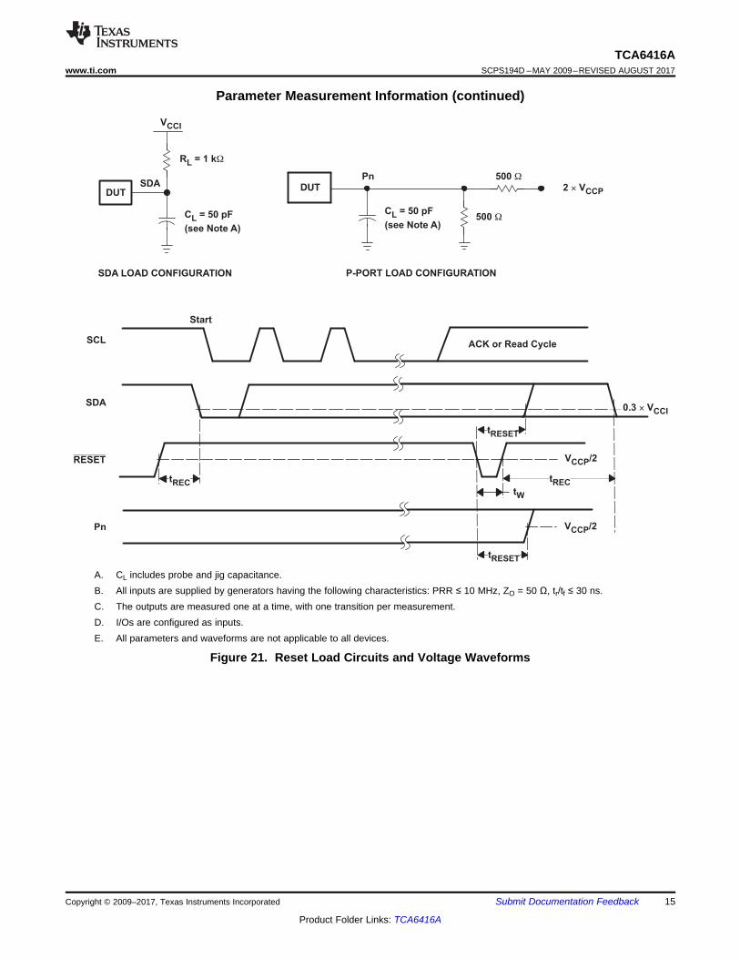
6.7 Reset Timing Requirementsover recommended operating free-air temperature range (unless otherwise noted) (see Figure 21)
STANDARD MODEI2C BUS
FAST MODEI2C BUS UNIT
MIN MAX MIN MAXtW Reset pulse duration 4 4 nstREC Reset recovery time 0 0 nstRESET Time to reset (1) 600 600 ns
6.8 Switching Characteristicsover recommended operating free-air temperature range, CL ≤ 100 pF (unless otherwise noted) (see Figure 18)
PARAMETER FROM TO
STANDARDMODE
I2C BUS
FAST MODEI2C BUS
UNIT
MIN MAX MIN MAXtIV Interrupt valid time P port INT 4 4 µstIR Interrupt reset delay time SCL INT 4 4 µstPV Output data valid SCL P7–P0 400 400 nstPS Input data setup time P port SCL 0 0 nstPH Input data hold time P port SCL 300 300 ns
A. CL includes probe and jig capacitance. tocf is measured with CL of 10 pF or 400 pF.B. All inputs are supplied by generators having the following characteristics: PRR ≤ 10 MHz, ZO = 50 Ω, tr/tf ≤ 30 ns.C. All parameters and waveforms are not applicable to all devices.
Figure 18. I2C Interface Load Circuit And Voltage Waveforms
A. CL includes probe and jig capacitance.B. All inputs are supplied by generators having the following characteristics: PRR ≤ 10 MHz, ZO = 50 Ω, tr/tf ≤ 30 ns.C. All parameters and waveforms are not applicable to all devices.
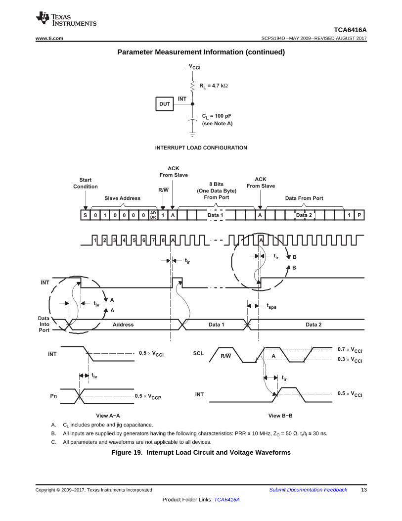
Figure 19. Interrupt Load Circuit and Voltage Waveforms
A. CL includes probe and jig capacitance.B. tpv is measured from 0.7 × VCC on SCL to 50% I/O (Pn) output.C. All inputs are supplied by generators having the following characteristics: PRR ≤ 10 MHz, ZO = 50 Ω, tr/tf ≤ 30 ns.D. The outputs are measured one at a time, with one transition per measurement.E. All parameters and waveforms are not applicable to all devices.
Figure 20. P-Port Load Circuit and Timing Waveforms
A. CL includes probe and jig capacitance.B. All inputs are supplied by generators having the following characteristics: PRR ≤ 10 MHz, ZO = 50 Ω, tr/tf ≤ 30 ns.C. The outputs are measured one at a time, with one transition per measurement.D. I/Os are configured as inputs.E. All parameters and waveforms are not applicable to all devices.
Figure 21. Reset Load Circuits and Voltage Waveforms
8.1 OverviewThe TCA6416A is a 16-bit I/O expander for the two-line bidirectional bus (I2C) is designed for 1.65-V to 5.5-Voperation. It provides general-purpose remote I/O expansion and bidirectional voltage translation for processorsthrough I2C communication, an interface consisting of serial clock (SCL), and serial data (SDA) signals.
The major benefit of the TCA6416A is its voltage translation capability over a of a wide supply voltage range.This allows the TCA6416A to interface with modern processors on the I2C side, where supply levels are lower toconserve power. In contrast to the dropping power supplies of processors, some PCB components such asLEDs, still require a 5-V power supply.
The VCCI pin is the power supply for the I2C bus, and therefore the pull-up resistors connected to the SCL, SDA,INT, and RESET pins should be terminated at VCCI on the opposite side. level of the I2C bus to the TCA6416A.The VCCP pin is the power supply for the P-ports and if pull-up resistors are used on any P-port or LEDs aredriven by any P-port, then the resistor(s) or LED(s) connected to P00-P07 and P10-P17 should be terminated atVCCP on the opposite side. The device P-ports configured as outputs have the ability to sink up to 25 mA fordirectly driving LEDs, but the current must be limited externally with an additional resistance.
The features of the device include an interrupt that is generated on the INT pin whenever an input port changesstate. The devices can also be reset to its default state by applying a low logic level to the RESET pin or bycycling power to the device and causing a power-on reset. The ADDR hardware selectable address pin allowstwo TCA6416A devices to be connected to the same I2C bus.
The TCA6416A open-drain interrupt (INT) output is activated when any input state differs from its correspondingInput Port register state and is used to indicate to the system master that an input state has changed. The INTpin can be connected to the interrupt input of a processor. By sending an interrupt signal on this line, theTCA6416A can inform the processor if there is incoming data on the remote I/O ports without having tocommunicate via the I2C bus. Thus, the TCA6416A can remain a simple slave device.
The system master can reset the TCA6416A in the event of a timeout or other improper operation by asserting alow on the RESET input pin or by cycling the power to the VCCP pin and causing a power-on reset (POR). Areset puts the registers in their default state and initializes the I2C /SMBus state machine. The RESET featureand a POR cause the same reset/initialization to occur, but the RESET feature does so without powering downthe part.
One hardware pin (ADDR) can be used to program and vary the fixed I2C address and allow two devices toshare the same I2C bus or SMBus.
The TCA6416A's digital core consists of eight 8-bit data registers: two Configuration registers (input or outputselection), two Input Port registers, two Output Port registers, and two Polarity Inversion registers. At power on orafter a reset, the I/Os are configured as inputs. However, the system master can configure the I/Os as eitherinputs or outputs by writing to the Configuration registers. The data for each input or output is kept in thecorresponding Input Port or Output Port register. The polarity of the Input Port register can be inverted with thePolarity Inversion register. All registers can be read by the system master.
8.3.1 Voltage TranslationTable 2 lists all of the optional voltage supply level combinations for the I2C bus (VCCI) and the P-ports (VCCP)supported by the TCA6416A.
Table 2. Voltage TranslationVCCI (SDA AND SCL OF I2C MASTER)
8.3.2 I/O PortWhen an I/O is configured as an input, FETs Q1 and Q2 are off, which creates a high-impedance input. Theinput voltage may be raised above VCC to a maximum of 5.5 V.
If the I/O is configured as an output, Q1 or Q2 is enabled, depending on the state of the output port register. Inthis case, there are low-impedance paths between the I/O pin and either VCC or GND. The external voltageapplied to this I/O pin should not exceed the recommended levels for proper operation.
8.3.3 Interrupt Output (INT)An interrupt is generated by any rising or falling edge of the port inputs in the input mode. After time tiv, the signalINT is valid. Resetting the interrupt circuit is achieved when data on the port is changed to the original setting orwhen data is read from the port that generated the interrupt. Resetting occurs in the read mode at theacknowledge (ACK) or not acknowledge (NACK) bit after the rising edge of the SCL signal. Interrupts that occurduring the ACK or NACK clock pulse can be lost (or be very short) due to the resetting of the interrupt during thispulse. Each change of the I/Os after resetting is detected and is transmitted as INT.
Reading from or writing to another device does not affect the interrupt circuit, and a pin configured as an outputcannot cause an interrupt. Changing an I/O from an output to an input may cause a false interrupt to occur, if thestate of the pin does not match the contents of the Input Port register.
The INT output has an open-drain structure and requires pull-up resistor to VCCP or VCCI depending on theapplication. INT should be connected to the voltage source of the device that requires the interrupt information.
8.3.4 Reset Input (RESET)The RESET input can be asserted to initialize the system while keeping the VCCP at its operating level. A resetcan be accomplished by holding the RESET pin low for a minimum of tW. The TCA6416A registers andI2C/SMBus state machine are changed to their default state once RESET is low (0). When RESET is high (1),the I/O levels at the P port can be changed externally or through the master. This input requires a pull-up resistorto VCCI, if no active connection is used.
8.4.1 Power-On ResetWhen power (from 0 V) is applied to VCCP, an internal power-on reset holds the TCA6416A in a reset conditionuntil VCCP has reached VPOR. At that time, the reset condition is released, and the TCA6416A registers andI2C/SMBus state machine initializes to their default states. After that, VCCP must be lowered to below VPORF andback up to the operating voltage for a power-reset cycle.
8.5 Programming
8.5.1 I2C InterfaceThe bidirectional I2C bus consists of the serial clock (SCL) and serial data (SDA) lines. Both lines must beconnected to a positive supply through a pull-up resistor when connected to the output stages of a device. Datatransfer may be initiated only when the bus is not busy.
I2C communication with this device is initiated by a master sending a Start condition, a high-to-low transition onthe SDA input/output, while the SCL input is high (see Figure 24). After the Start condition, the device addressbyte is sent, most significant bit (MSB) first, including the data direction bit (R/W).
After receiving the valid address byte, this device responds with an acknowledge (ACK), a low on the SDAinput/output during the high of the ACK-related clock pulse. The address (ADDR) input of the slave device mustnot be changed between the Start and the Stop conditions.
On the I2C bus, only one data bit is transferred during each clock pulse. The data on the SDA line must remainstable during the high pulse of the clock period, as changes in the data line at this time are interpreted as controlcommands (Start or Stop) (see Figure 25).
A Stop condition, a low-to-high transition on the SDA input/output while the SCL input is high, is sent by themaster (see Figure 24).
Any number of data bytes can be transferred from the transmitter to receiver between the Start and the Stopconditions. Each byte of eight bits is followed by one ACK bit. The transmitter must release the SDA line beforethe receiver can send an ACK bit. The device that acknowledges must pull down the SDA line during the ACKclock pulse, so that the SDA line is stable low during the high pulse of the ACK-related clock period (seeFigure 26). When a slave receiver is addressed, it must generate an ACK after each byte is received. Similarly,the master must generate an ACK after each byte that it receives from the slave transmitter. Setup and holdtimes must be met to ensure proper operation.
A master receiver signals an end of data to the slave transmitter by not generating an acknowledge (NACK) afterthe last byte has been clocked out of the slave. This is done by the master receiver by holding the SDA line high.In this event, the transmitter must release the data line to enable the master to generate a Stop condition.
Figure 24. Definition of Start and Stop Conditions
The last bit of the slave address defines the operation (read or write) to be performed. A high (1) selects a readoperation, while a low (0) selects a write operation.
8.6.2 Control Register and Command ByteFollowing the successful acknowledgment of the address byte, the bus master sends a command byte, which isstored in the control register in the TCA6416A. Three bits of this data byte state the operation (read or write) andthe internal registers (input, output, polarity inversion, or configuration) that will be affected. This register can bewritten or read through the I2C bus. The command byte is sent only during a write transmission.
Once a new command has been sent, the register that was addressed continues to be accessed by reads until anew command byte has been sent.
8.6.3 Register DescriptionsThe Input Port registers (registers 0 and 1) reflect the incoming logic levels of the pins, regardless of whether thepin is defined as an input or an output by the Configuration register. They act only on read operation. Writes tothese registers have no effect. The default value (X) is determined by the externally applied logic level. Before aread operation, a write transmission is sent with the command byte to indicate to the I2C device that the InputPort register will be accessed next.
Table 6. Registers 0 and 1 (Input Port Registers)BIT I-07 I-06 I-05 I-04 I-03 I-02 I-01 I-00
DEFAULT X X X X X X X XBIT I-17 I-16 I-15 I-14 I-13 I-12 I-11 I-10
DEFAULT X X X X X X X X
The Output Port registers (registers 2 and 3) shows the outgoing logic levels of the pins defined as outputs bythe Configuration register. Bit values in these registers have no effect on pins defined as inputs. In turn, readsfrom these registers reflect the value that is in the flip-flop controlling the output selection, not the actual pinvalue.
Table 7. Registers 2 and 3 (Output Port Registers)BIT O-07 O-06 O-05 O-04 O-03 O-02 O-01 O-00
The Polarity Inversion registers (register 4 and 5) allow polarity inversion of pins defined as inputs by theConfiguration register. If a bit in these registers is set (written with 1), the corresponding port pin's polarity isinverted. If a bit in these registers is cleared (written with a 0), the corresponding port pin's original polarity isretained.
The Configuration registers (registers 6 and 7) configure the direction of the I/O pins. If a bit in these registers isset to 1, the corresponding port pin is enabled as an input with a high-impedance output driver. If a bit in theseregisters is cleared to 0, the corresponding port pin is enabled as an output.
8.6.4 Bus TransactionsData is exchanged between the master and TCA6416A through write and read commands.
8.6.4.1 WritesData is transmitted to the TCA6416A by sending the device address and setting the least-significant bit (LSB) toa logic 0 (see Figure 27 for device address). The command byte is sent after the address and determines whichregister receives the data that follows the command byte. There is no limitation on the number of data bytes sentin one write transmission.
The eight registers within the TCA6416A are configured to operate as four register pairs. The four pairs are inputports, output ports, polarity inversion ports and configuration ports. After sending data to one register, the nextdata byte is sent to the other register in the pair (see Figure 29 and Figure 30). For example, if the first byte issend to Output Port 1 (register 3), the next byte is stored in Output Port 0 (register 2).
There is no limitation on the number of data bytes sent in one write transmission. In this way, each 8-bit registermay be updated independently of the other registers.
Figure 30. Write to Configuration or Polarity Inversion Registers
8.6.4.2 ReadsThe bus master first must send the TCA6416A address with the LSB set to a logic 0 (see Figure 27 for deviceaddress). The command byte is sent after the address and determines which register is accessed.
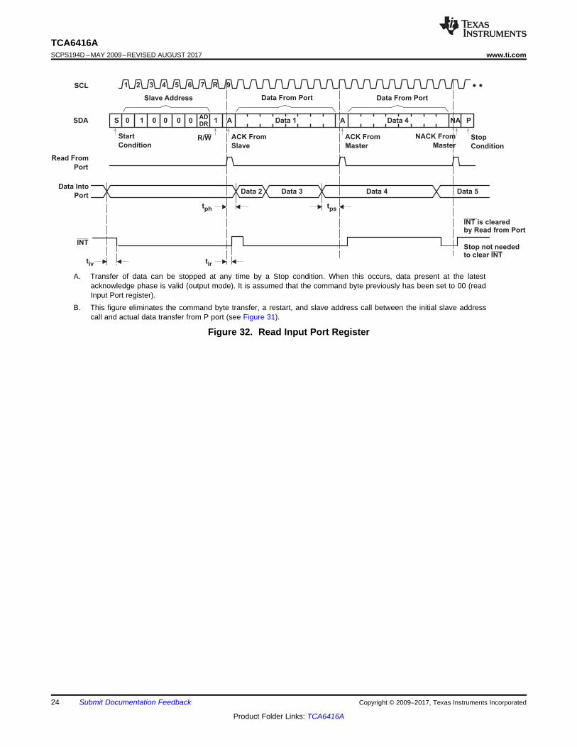
After a restart, the device address is sent again but, this time, the LSB is set to a logic 1. Data from the registerdefined by the command byte then is sent by the TCA6416A (see Figure 31 and Figure 32).
After a restart, the value of the register defined by the command byte matches the register being accessed whenthe restart occurred. For example, if the command byte references Input Port 1 before the restart, and the restartoccurs when Input Port 0 is being read, the stored command byte changes to reference Input Port 0. The originalcommand byte is forgotten. If a subsequent restart occurs, Input Port 0 is read first. Data is clocked into theregister on the rising edge of the ACK clock pulse. After the first byte is read, additional bytes may be read, butthe data now reflects the information in the other register in the pair. For example, if Input Port 1 is read, the nextbyte read is Input Port 0.
Data is clocked into the register on the rising edge of the ACK clock pulse. There is no limitation on the numberof data bytes received in one read transmission, but when the final byte is received, the bus master must notacknowledge the data.
A. Transfer of data can be stopped at any time by a Stop condition. When this occurs, data present at the latestacknowledge phase is valid (output mode). It is assumed that the command byte previously has been set to 00 (readInput Port register).
B. This figure eliminates the command byte transfer, a restart, and slave address call between the initial slave addresscall and actual data transfer from P port (see Figure 31).
NOTEInformation in the following applications sections is not part of the TI componentspecification, and TI does not warrant its accuracy or completeness. TI’s customers areresponsible for determining suitability of components for their purposes. Customers shouldvalidate and test their design implementation to confirm system functionality.
9.1 Application InformationApplications of the TCA6416A will have this device connected as a slave to an I2C master (processor), and theI2C bus may contain any number of other slave devices. The TCA6416A will be in a remote location from themaster, placed close to the GPIOs to which the master needs to monitor or control.
A typical application of the TCA6416A will operate with a lower voltage on the master side (VCCI), and a highervoltage on the P-port side (VCCP). The P-ports can be configured as outputs connected to inputs of devicessuch as enable, reset, power select, the gate of a switch, and LEDs. The P-ports can also be configured asinputs to receive data from interrupts, alarms, status outputs, or push buttons.
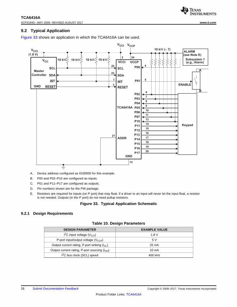
9.2 Typical ApplicationFigure 33 shows an application in which the TCA6416A can be used.
A. Device address configured as 0100000 for this example.B. P00 and P02–P10 are configured as inputs.C. P01 and P11–P17 are configured as outputs.D. Pin numbers shown are for the PW package.E. Resistors are required for inputs (on P port) that may float. If a driver to an input will never let the input float, a resistor
is not needed. Outputs (in the P port) do not need pullup resistors.
Figure 33. Typical Application Schematic
9.2.1 Design Requirements
Table 10. Design ParametersDESIGN PARAMETER EXAMPLE VALUEI2C input voltage (VCCI) 1.8 V
P-port input/output voltage (VCCP) 5 VOutput current rating, P-port sinking (IOL) 25 mA
Output current rating, P-port sourcing (IOH) 10 mAI2C bus clock (SCL) speed 400 kHz
9.2.2 Detailed Design ProcedureThe pull-up resistors, RP, for the SCL and SDA lines need to be selected appropriately and take intoconsideration the total capacitance of all slaves on the I2C bus. The minimum pull-up resistance is a function ofVCC, VOL,(max), and IOL:
(1)
The maximum pull-up resistance is a function of the maximum rise time, tr (300 ns for fast-mode operation, fSCL =400 kHz) and bus capacitance, Cb:
(2)
The maximum bus capacitance for an I2C bus must not exceed 400 pF for standard-mode or fast-modeoperation. The bus capacitance can be approximated by adding the capacitance of the TCA9538, Ci for SCL orCio for SDA, the capacitance of wires/connections/traces, and the capacitance of additional slaves on the bus.
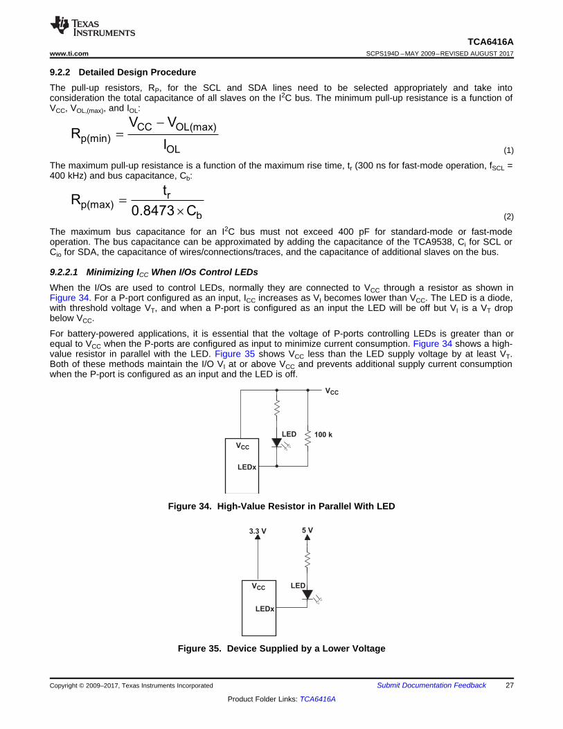
9.2.2.1 Minimizing ICC When I/Os Control LEDsWhen the I/Os are used to control LEDs, normally they are connected to VCC through a resistor as shown inFigure 34. For a P-port configured as an input, ICC increases as VI becomes lower than VCC. The LED is a diode,with threshold voltage VT, and when a P-port is configured as an input the LED will be off but VI is a VT dropbelow VCC.
For battery-powered applications, it is essential that the voltage of P-ports controlling LEDs is greater than orequal to VCC when the P-ports are configured as input to minimize current consumption. Figure 34 shows a high-value resistor in parallel with the LED. Figure 35 shows VCC less than the LED supply voltage by at least VT.Both of these methods maintain the I/O VI at or above VCC and prevents additional supply current consumptionwhen the P-port is configured as an input and the LED is off.
Figure 34. High-Value Resistor in Parallel With LED
(1) TA = 25°C (unless otherwise noted).(2) Not tested. Specified by design.
10 Power Supply Recommendations
10.1 Power-On Reset RequirementsIn the event of a glitch or data corruption, TCA6416A can be reset to its default conditions by using the power-onreset feature. Power-on reset requires that the device go through a power cycle to be completely reset. Thisreset also happens when the device is powered on for the first time in an application.
The two types of power-on reset are shown in Figure 38 and Figure 39.
Figure 38. VCC is Lowered Below 0.2 V or 0 V and Then Ramped up to VCC
Figure 39. VCC is Lowered Below the POR Threshold, Then Ramped Back up to VCC
Table 11 specifies the performance of the power-on reset feature for TCA6416A for both types of power-on reset.
Table 11. Recommended Supply Sequencing and Ramp Rates (1) (2)
PARAMETER MIN TYP MAX UNITtFT Fall rate See Figure 38 0.1 2000 mstRT Rise rate See Figure 38 0.1 2000 mstTRR_GND Time to re-ramp (when VCC drops to GND) See Figure 38 1 μstTRR_POR50 Time to re-ramp (when VCC drops to VPOR_MIN – 50 mV) See Figure 39 1 μs
VCC_GHLevel that VCCP can glitch down to, but not cause a functionaldisruption when VCCX_GW = 1 μs See Figure 40 1.2 V
tGWGlitch width that will not cause a functional disruption whenVCCX_GH = 0.5 × VCCx
See Figure 40 10 μs
VPORF Voltage trip point of POR on falling VCC 0.7 VVPORR Voltage trip point of POR on fising VCC 1.4 V
Glitches in the power supply can also affect the power-on reset performance of this device. The glitch width(VCC_GW) and height (VCC_GH) are dependent on each other. The bypass capacitance, source impedance, anddevice impedance are factors that affect power-on reset performance. Figure 40 and Table 11 provide moreinformation on how to measure these specifications.
Figure 40. Glitch Width and Glitch Height
VPOR is critical to the power-on reset. VPOR is the voltage level at which the reset condition is released and all theregisters and the I2C/SMBus state machine are initialized to their default states. The value of VPOR differs basedon the VCC being lowered to or from 0. Figure 41 and Table 11 provide more details on this specification.
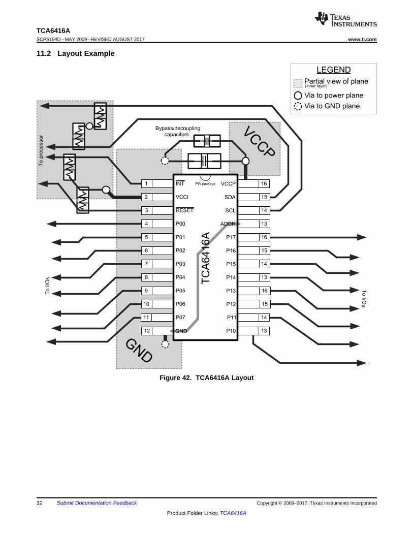
11.1 Layout GuidelinesFor printed circuit board (PCB) layout of the TCA6416A, common PCB layout practices should be followedbut additional concerns related to high-speed data transfer such as matched impedances and differentialpairs are not a concern for I2C signal speeds.In all PCB layouts, it is a best practice to avoid right angles in signal traces, to fan out signal traces awayfrom each other upon leaving the vicinity of an integrated circuit (IC), and to use thicker trace widths to carryhigher amounts of current that commonly pass through power and ground traces. By-pass and de-couplingcapacitors are commonly used to control the voltage on the VCCP pin, using a larger capacitor to provideadditional power in the event of a short power supply glitch and a smaller capacitor to filter out high-frequency ripple. These capacitors should be placed as close to the TCA6416A as possible. These bestpractices are shown in Figure 42.For the layout example provided in Figure 42, it would be possible to fabricate a PCB with only 2 layers byusing the top layer for signal routing and the bottom layer as a split plane for power (VCCI and VCCP) andground (GND). However, a 4 layer board is preferable for boards with higher density signal routing. On a 4layer PCB, it is common to route signals on the top and bottom layer, dedicate one internal layer to a groundplane, and dedicate the other internal layer to a power plane. In a board layout using planes or split planesfor power and ground, vias are placed directly next to the surface mount component pad which needs toattach to VCCI, VCCP, or GND and the via is connected electrically to the internal layer or the other side of theboard. Vias are also used when a signal trace needs to be routed to the opposite side of the board, but thistechnique is not demonstrated in Figure 42.
12.1 TrademarksAll trademarks are the property of their respective owners.
12.2 Electrostatic Discharge CautionThese devices have limited built-in ESD protection. The leads should be shorted together or the device placed in conductive foamduring storage or handling to prevent electrostatic damage to the MOS gates.
12.3 GlossarySLYZ022 — TI Glossary.
This glossary lists and explains terms, acronyms, and definitions.
13 Mechanical, Packaging, and Orderable InformationThe following pages include mechanical, packaging, and orderable information. This information is the mostcurrent data available for the designated devices. This data is subject to change without notice and revision ofthis document. For browser-based versions of this data sheet, refer to the left-hand navigation.
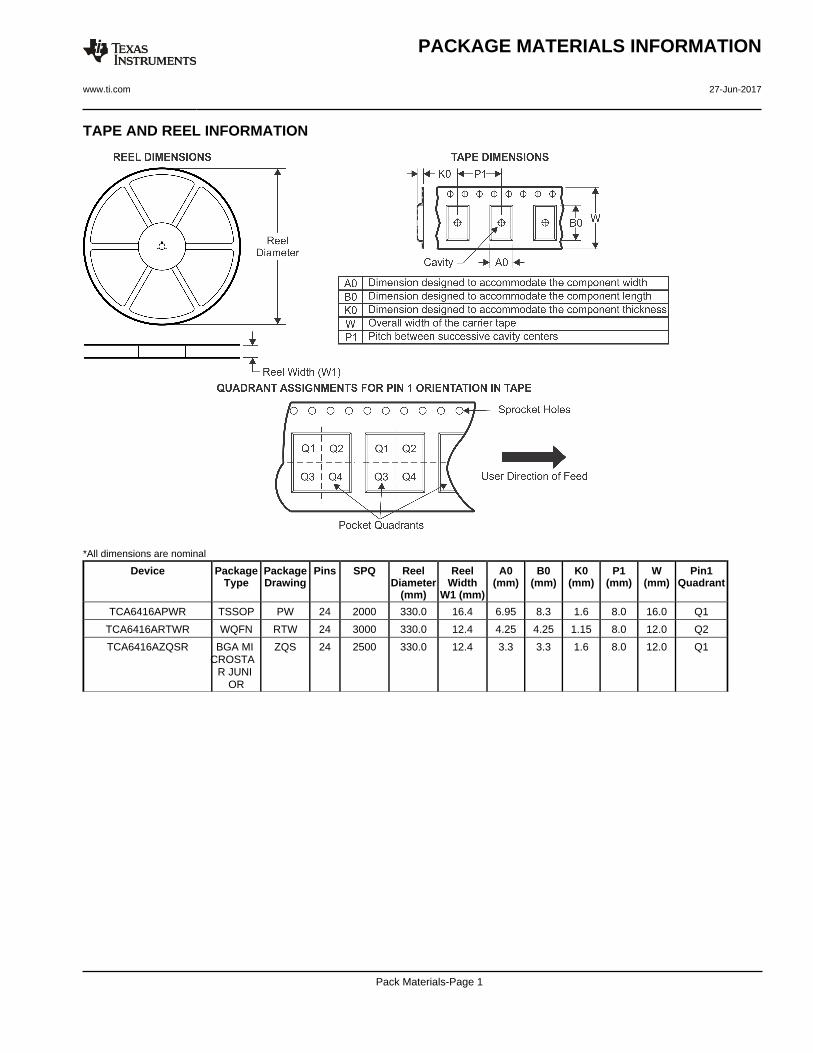
TCA6416APWR ACTIVE TSSOP PW 24 2000 Green (RoHS& no Sb/Br)
CU NIPDAU Level-1-260C-UNLIM -40 to 85 PH416A
TCA6416ARTWR ACTIVE WQFN RTW 24 3000 Green (RoHS& no Sb/Br)
CU NIPDAU Level-2-260C-1 YEAR -40 to 85 PH416A
TCA6416AZQSR ACTIVE BGAMICROSTAR
JUNIOR
ZQS 24 2500 Green (RoHS& no Sb/Br)
SNAGCU Level-1-260C-UNLIM -40 to 85 PH416A
(1) The marketing status values are defined as follows:ACTIVE: Product device recommended for new designs.LIFEBUY: TI has announced that the device will be discontinued, and a lifetime-buy period is in effect.NRND: Not recommended for new designs. Device is in production to support existing customers, but TI does not recommend using this part in a new design.PREVIEW: Device has been announced but is not in production. Samples may or may not be available.OBSOLETE: TI has discontinued the production of the device.
(2) RoHS: TI defines "RoHS" to mean semiconductor products that are compliant with the current EU RoHS requirements for all 10 RoHS substances, including the requirement that RoHS substancedo not exceed 0.1% by weight in homogeneous materials. Where designed to be soldered at high temperatures, "RoHS" products are suitable for use in specified lead-free processes. TI mayreference these types of products as "Pb-Free".RoHS Exempt: TI defines "RoHS Exempt" to mean products that contain lead but are compliant with EU RoHS pursuant to a specific EU RoHS exemption.Green: TI defines "Green" to mean the content of Chlorine (Cl) and Bromine (Br) based flame retardants meet JS709B low halogen requirements of <=1000ppm threshold. Antimony trioxide basedflame retardants must also meet the <=1000ppm threshold requirement.
(3) MSL, Peak Temp. - The Moisture Sensitivity Level rating according to the JEDEC industry standard classifications, and peak solder temperature.
(4) There may be additional marking, which relates to the logo, the lot trace code information, or the environmental category on the device.
(5) Multiple Device Markings will be inside parentheses. Only one Device Marking contained in parentheses and separated by a "~" will appear on a device. If a line is indented then it is a continuationof the previous line and the two combined represent the entire Device Marking for that device.
(6) Lead/Ball Finish - Orderable Devices may have multiple material finish options. Finish options are separated by a vertical ruled line. Lead/Ball Finish values may wrap to two lines if the finishvalue exceeds the maximum column width.
Important Information and Disclaimer:The information provided on this page represents TI's knowledge and belief as of the date that it is provided. TI bases its knowledge and belief on informationprovided by third parties, and makes no representation or warranty as to the accuracy of such information. Efforts are underway to better integrate information from third parties. TI has taken andcontinues to take reasonable steps to provide representative and accurate information but may not have conducted destructive testing or chemical analysis on incoming materials and chemicals.TI and TI suppliers consider certain information to be proprietary, and thus CAS numbers and other limited information may not be available for release.
In no event shall TI's liability arising out of such information exceed the total purchase price of the TI part(s) at issue in this document sold by TI to Customer on an annual basis.
1. All linear dimensions are in millimeters. Any dimensions in parenthesis are for reference only. Dimensioning and tolerancingper ASME Y14.5M.
2. This drawing is subject to change without notice.
PACKAGE OUTLINE
4219135/A 11/2016
www.ti.com
WQFN - 0.8 mm max height
PLASTIC QUAD FLATPACK-NO LEAD
RTW0024B
A
0.08 C
0.1 C A B0.05 C
B
SYMM
SYMM
4.13.9
4.13.9
PIN 1 INDEX AREA
0.8 MAX
0.050.00
C
SEATING PLANE
PIN 1 ID(OPTIONAL)
2X2.5
20X 0.5
2X 2.5
1
6
18
13
7 12
24 19
2.45±0.1
24X 0.340.24
24X 0.50.3
(0.2) TYP
25
EXPOSEDTHERMAL PAD
NOTES: (continued)
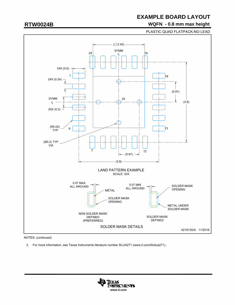
3. For more information, see Texas Instruments literature number SLUA271 (www.ti.com/lit/slua271) .
EXAMPLE BOARD LAYOUT
4219135/A 11/2016
www.ti.com
WQFN - 0.8 mm max height
RTW0024B
PLASTIC QUAD FLATPACK-NO LEAD
SYMM
SYMM
LAND PATTERN EXAMPLESCALE: 20X
( 2.45)
24X (0.6)
24X (0.24)1
6
7 12
13
18
1924
(3.8)
(0.97)
(3.8)
(0.97)
25
(R0.05) TYP
20X (0.5)
(Ø0.2) TYPVIA
0.07 MAXALL AROUND 0.07 MIN
ALL AROUNDMETAL
SOLDER MASKOPENING
SOLDER MASKOPENING
METAL UNDERSOLDER MASK
SOLDER MASK DETAILS
NON SOLDER MASKDEFINED
(PREFERRED)SOLDER MASK
DEFINED
NOTES: (continued)
4. Laser cutting apertures with trapezoidal walls and rounded corners may offer better paste release. IPC-7525 may have alternatedesign recommendations.
EXAMPLE STENCIL DESIGN
4219135/A 11/2016
www.ti.com
WQFN - 0.8 mm max height
RTW0024B
PLASTIC QUAD FLATPACK-NO LEAD
SYMM
SYMM
SOLDER PASTE EXAMPLEBASED ON 0.125 mm THICK STENCIL
EXPOSED PAD 25:78% PRINTED COVERAGE BY AREA UNDER PACKAGE
SCALE: 20X
(3.8)
(0.64) TYP
1
6
7 12
13
18
1924
25
(0.64) TYP
4X( 1.08)
(R0.05) TYP
(3.8)
20X (0.5)
24X (0.24)
24X (0.6)
METALTYP
IMPORTANT NOTICE
Texas Instruments Incorporated (TI) reserves the right to make corrections, enhancements, improvements and other changes to itssemiconductor products and services per JESD46, latest issue, and to discontinue any product or service per JESD48, latest issue. Buyersshould obtain the latest relevant information before placing orders and should verify that such information is current and complete.TI’s published terms of sale for semiconductor products (http://www.ti.com/sc/docs/stdterms.htm) apply to the sale of packaged integratedcircuit products that TI has qualified and released to market. Additional terms may apply to the use or sale of other types of TI products andservices.Reproduction of significant portions of TI information in TI data sheets is permissible only if reproduction is without alteration and isaccompanied by all associated warranties, conditions, limitations, and notices. TI is not responsible or liable for such reproduceddocumentation. Information of third parties may be subject to additional restrictions. Resale of TI products or services with statementsdifferent from or beyond the parameters stated by TI for that product or service voids all express and any implied warranties for theassociated TI product or service and is an unfair and deceptive business practice. TI is not responsible or liable for any such statements.Buyers and others who are developing systems that incorporate TI products (collectively, “Designers”) understand and agree that Designersremain responsible for using their independent analysis, evaluation and judgment in designing their applications and that Designers havefull and exclusive responsibility to assure the safety of Designers' applications and compliance of their applications (and of all TI productsused in or for Designers’ applications) with all applicable regulations, laws and other applicable requirements. Designer represents that, withrespect to their applications, Designer has all the necessary expertise to create and implement safeguards that (1) anticipate dangerousconsequences of failures, (2) monitor failures and their consequences, and (3) lessen the likelihood of failures that might cause harm andtake appropriate actions. Designer agrees that prior to using or distributing any applications that include TI products, Designer willthoroughly test such applications and the functionality of such TI products as used in such applications.TI’s provision of technical, application or other design advice, quality characterization, reliability data or other services or information,including, but not limited to, reference designs and materials relating to evaluation modules, (collectively, “TI Resources”) are intended toassist designers who are developing applications that incorporate TI products; by downloading, accessing or using TI Resources in anyway, Designer (individually or, if Designer is acting on behalf of a company, Designer’s company) agrees to use any particular TI Resourcesolely for this purpose and subject to the terms of this Notice.TI’s provision of TI Resources does not expand or otherwise alter TI’s applicable published warranties or warranty disclaimers for TIproducts, and no additional obligations or liabilities arise from TI providing such TI Resources. TI reserves the right to make corrections,enhancements, improvements and other changes to its TI Resources. TI has not conducted any testing other than that specificallydescribed in the published documentation for a particular TI Resource.Designer is authorized to use, copy and modify any individual TI Resource only in connection with the development of applications thatinclude the TI product(s) identified in such TI Resource. NO OTHER LICENSE, EXPRESS OR IMPLIED, BY ESTOPPEL OR OTHERWISETO ANY OTHER TI INTELLECTUAL PROPERTY RIGHT, AND NO LICENSE TO ANY TECHNOLOGY OR INTELLECTUAL PROPERTYRIGHT OF TI OR ANY THIRD PARTY IS GRANTED HEREIN, including but not limited to any patent right, copyright, mask work right, orother intellectual property right relating to any combination, machine, or process in which TI products or services are used. Informationregarding or referencing third-party products or services does not constitute a license to use such products or services, or a warranty orendorsement thereof. Use of TI Resources may require a license from a third party under the patents or other intellectual property of thethird party, or a license from TI under the patents or other intellectual property of TI.TI RESOURCES ARE PROVIDED “AS IS” AND WITH ALL FAULTS. TI DISCLAIMS ALL OTHER WARRANTIES ORREPRESENTATIONS, EXPRESS OR IMPLIED, REGARDING RESOURCES OR USE THEREOF, INCLUDING BUT NOT LIMITED TOACCURACY OR COMPLETENESS, TITLE, ANY EPIDEMIC FAILURE WARRANTY AND ANY IMPLIED WARRANTIES OFMERCHANTABILITY, FITNESS FOR A PARTICULAR PURPOSE, AND NON-INFRINGEMENT OF ANY THIRD PARTY INTELLECTUALPROPERTY RIGHTS. TI SHALL NOT BE LIABLE FOR AND SHALL NOT DEFEND OR INDEMNIFY DESIGNER AGAINST ANY CLAIM,INCLUDING BUT NOT LIMITED TO ANY INFRINGEMENT CLAIM THAT RELATES TO OR IS BASED ON ANY COMBINATION OFPRODUCTS EVEN IF DESCRIBED IN TI RESOURCES OR OTHERWISE. IN NO EVENT SHALL TI BE LIABLE FOR ANY ACTUAL,DIRECT, SPECIAL, COLLATERAL, INDIRECT, PUNITIVE, INCIDENTAL, CONSEQUENTIAL OR EXEMPLARY DAMAGES INCONNECTION WITH OR ARISING OUT OF TI RESOURCES OR USE THEREOF, AND REGARDLESS OF WHETHER TI HAS BEENADVISED OF THE POSSIBILITY OF SUCH DAMAGES.Unless TI has explicitly designated an individual product as meeting the requirements of a particular industry standard (e.g., ISO/TS 16949and ISO 26262), TI is not responsible for any failure to meet such industry standard requirements.Where TI specifically promotes products as facilitating functional safety or as compliant with industry functional safety standards, suchproducts are intended to help enable customers to design and create their own applications that meet applicable functional safety standardsand requirements. Using products in an application does not by itself establish any safety features in the application. Designers mustensure compliance with safety-related requirements and standards applicable to their applications. Designer may not use any TI products inlife-critical medical equipment unless authorized officers of the parties have executed a special contract specifically governing such use.Life-critical medical equipment is medical equipment where failure of such equipment would cause serious bodily injury or death (e.g., lifesupport, pacemakers, defibrillators, heart pumps, neurostimulators, and implantables). Such equipment includes, without limitation, allmedical devices identified by the U.S. Food and Drug Administration as Class III devices and equivalent classifications outside the U.S.TI may expressly designate certain products as completing a particular qualification (e.g., Q100, Military Grade, or Enhanced Product).Designers agree that it has the necessary expertise to select the product with the appropriate qualification designation for their applicationsand that proper product selection is at Designers’ own risk. Designers are solely responsible for compliance with all legal and regulatoryrequirements in connection with such selection.Designer will fully indemnify TI and its representatives against any damages, costs, losses, and/or liabilities arising out of Designer’s non-compliance with the terms and provisions of this Notice.


![F3JR MB R20 1211[31731]ncandelier.free.fr/asus/ASUS_F3JR_R20.pdfH_D#50 H_TMS H_TDO H_TCK H_TRST# H_PREQ# +VCCP +VCCP +VCCP +VCCP GND GND GND GND GND GND GND TPC26T 1 T1 R8 1 2 56Ohm](https://static.documents.pub/doc/80x56/5faf0ab01979a324157ec2b6/f3jr-mb-r20-121131731-hd50-htms-htdo-htck-htrst-hpreq-vccp-vccp-vccp.jpg)


