26
MEMORY
MEMORY

Moores Law for DRAM
2x increase in capacity every 18 months
2006: 4GB

Corollary to Moores Law
Cost / chip ~ constant (packaging)
Cost / bit = 2X reduction / 18 months
Current (2008) ~ 1 micro-cent / bit

Total Memory Production
2010
1E23 bits
produced
2006:
25% growth in for flash
memory for iPods
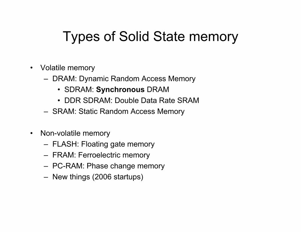
Types of Solid State memory
• Volatile memory
– DRAM: Dynamic Random Access Memory
• SDRAM: Synchronous DRAM
• DDR SDRAM: Double Data Rate SRAM
– SRAM: Static Random Access Memory
• Non-volatile memory
– FLASH: Floating gate memory
– FRAM: Ferroelectric memory
– PC-RAM: Phase change memory
– New things (2006 startups)

Memory Cell Read / Write
Word Line Read / Write enabled
Bit Line
Write
Bit Line
Read

SRAM CellStatic Random Access Memory
Word Line
Turn on read / write
Output
Negative
Output Out M1 M2 M3 M4
1 off on >> on off
0 on off >> off on
6 transistors
Holds state as long as voltage on
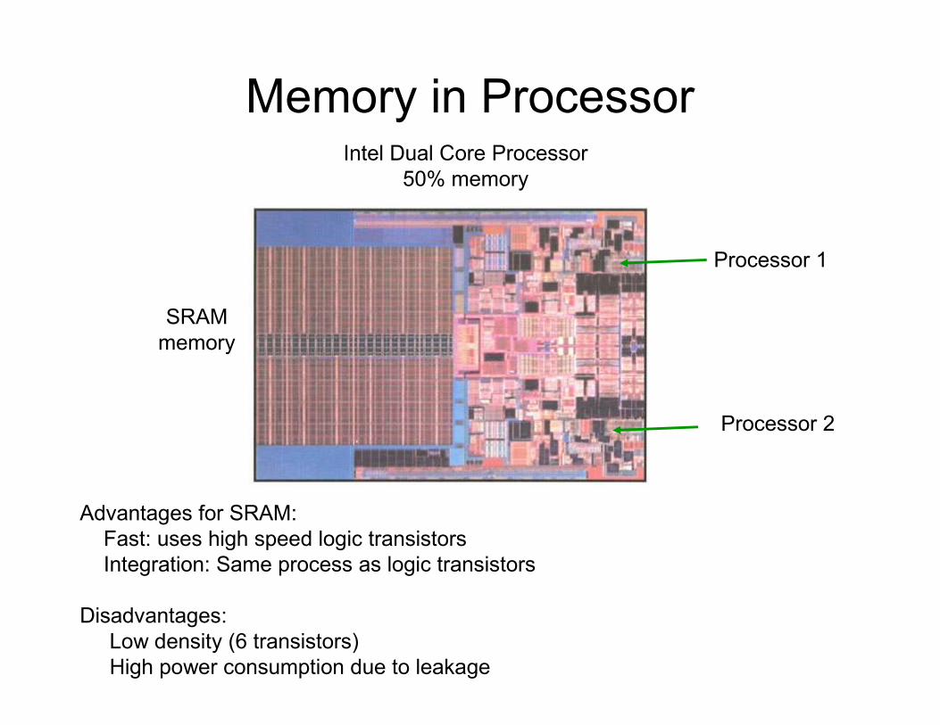
Memory in ProcessorIntel Dual Core Processor
50% memory
Processor 1
Processor 2
SRAM
memory
Advantages for SRAM:
Fast: uses high speed logic transistors
Integration: Same process as logic transistors
Disadvantages:
Low density (6 transistors)
High power consumption due to leakage

DRAMDynamic Random Access Memory
Wordline (row):
Enable read / write of capacitor
Bitline (column):
Capacitor charged = “1”
Capacitor not charged = “0”
Capacitor is storage element
Transistor enables read / write
Read:
Charge transferred to read
transistor
Write:
Bitline charged to Vdd or GNDMemory constantly being refreshed
Read / write cycle

DRAMStacked Capacitor
nFET
Capacitor leaks charge
���� More charge (capacitance) = longer refresh time
Dram requires large capacitance / area
Transistor
Conformal
oxide and
electrode
Rough surface
More area / cell

DRAMTrench Capacitor
nFET
Capacitor leaks charge
���� More charge (capacitance) = longer refresh time
Dram requires large capacitance / area
Deep trench for large area / cell
Thermal oxide + poly Si fill

Floating Gate NVRAMNon Volatile Random Access Memory
Gate Electrode isolated
� Minimum leakage sources
� Holds charge (no charge) indefinitely
� Electron Charge = transistor on
How to charge electrode?
Control Electrode isolated
� Charge in channel
� Carriers injected into floating gate
How to inject charge?
(a) Tunneling through oxide
(b) Hot carrier injection

Tunneling Through Barrier
Fowler-Nordheim
Tunneling
J ~ exp (-1/E)
Direct
Tunneling
Thermionic
Emmision
J~exp(V1/2)
Frenkel-Poole
Emmision
J~exp(V1/2)
Hot Carrier Injection
High field in S/D
High energy e/h pair
Easier to tunnel
Trap
Assisted

Hot Carrier Injection
Electrons gain
high kinetic energy (VD)
Bias is past pinch-off
Carriers injected into p-Si gap
with energy > Eg/2 Substrate biased positive
Electrons forced into gate
Gate negative
Holes injected

Charge / Clear Cycles
Charge
Cycle
Tunneling
(slow)
Injection
(fast)
Tunneling
(slow)
Clear
Cycle
Write Cycle faster
than clear cycle

Example of Floating Gate Flash

Charge Storage Flash
Floating Gate Problem:
Floating gate + control oxide add to device size
Gate oxides must be thick for reliability
Limited scaling to <90nm
Store charge within gate oxide (ONO)
SiN: high electron trap density = source of trapped charge

SiN as Charge “Sponge”
SiN >> SixNyHz
“Low quality” SiN has
trap states at specific
energy (Si dangling
bonds)
Charge Cycle Erase Cycle
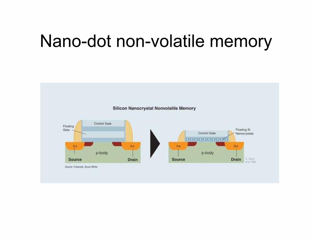
Nano-dot non-volatile memory

Current Flash Technology
Few hundred electons / gate * 1 billion gates

3-D Memory Cells
SiO2 “anti-fuse”
One time programmable
(OTP)
Stacked memory >>
� no limit to memory
cells / area
Currently in use for games
Matrix Semi. / Sandisk Inc.

New: Phase Change Memory
Word Line
Bit Line
Phase Change Material
Crystalline GeSbGe = low resistance
Heat material with Joule Heating…
Rapidly cool
Material freezes into:
Amorphous GeSbTe = high resistance
Similar technology to that for read/write CD disks
Potential for multi-level integration
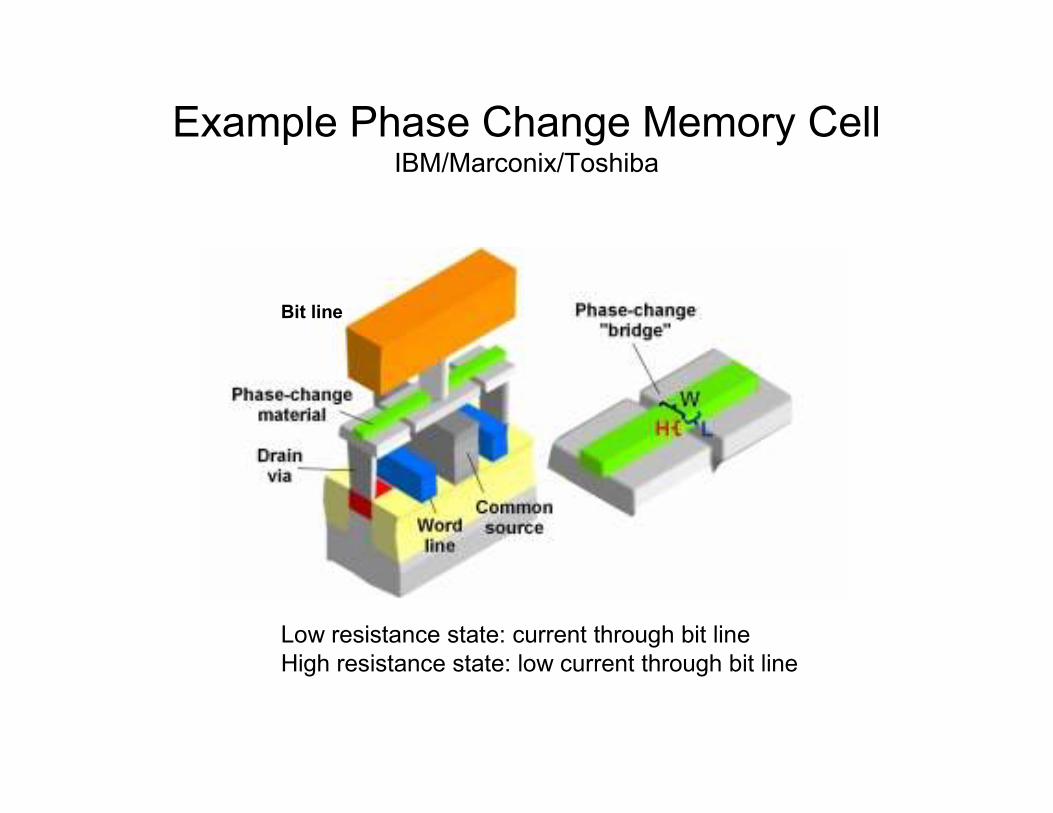
Example Phase Change Memory CellIBM/Marconix/Toshiba
Bit line
Low resistance state: current through bit line
High resistance state: low current through bit line
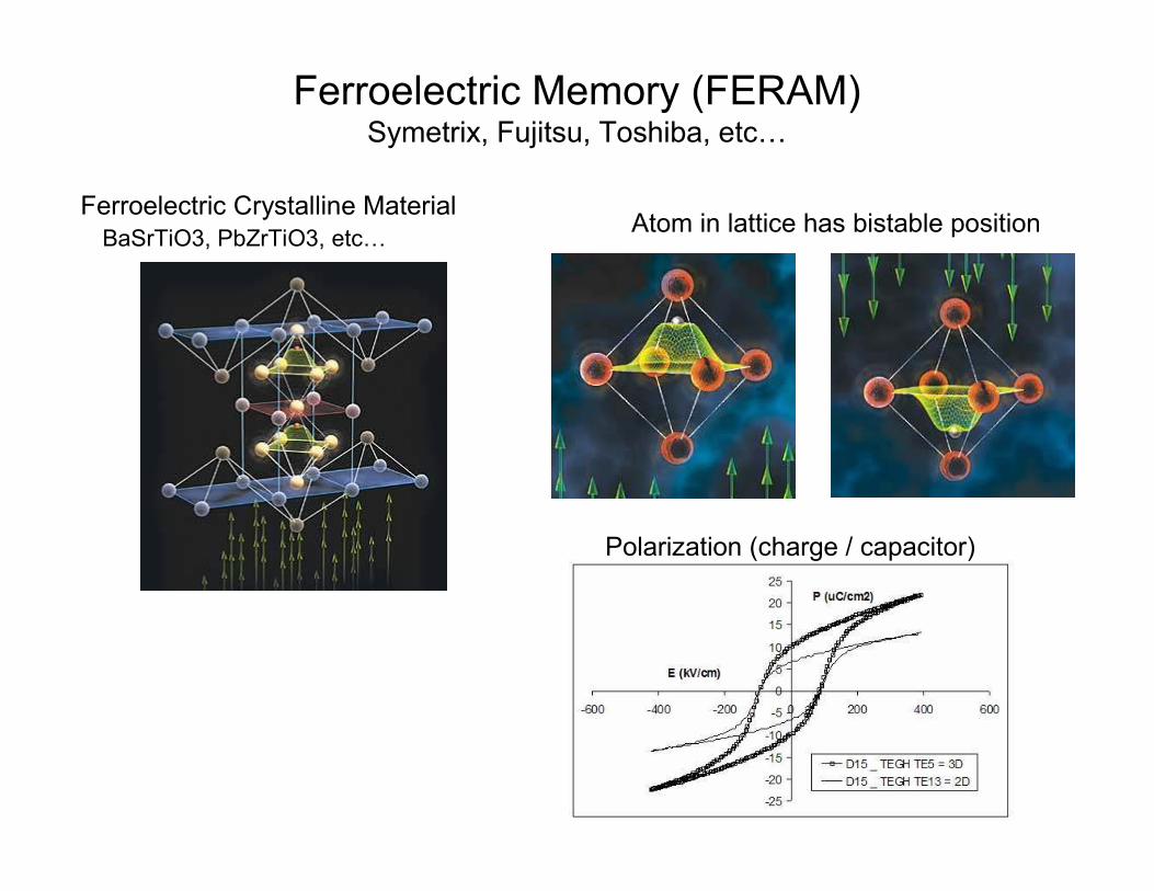
Ferroelectric Memory (FERAM)Symetrix, Fujitsu, Toshiba, etc…
Ferroelectric Crystalline Material
BaSrTiO3, PbZrTiO3, etc…Atom in lattice has bistable position
Polarization (charge / capacitor)

“Memresistor”HP, 2008
"There should be a device that remembers
how much current flowed through a device.“
= Memresistor
What about FLASH, DRAM, PC-RAM?
"It is a large amount of resistance change
with a small amount of [energy]."
Large memory Cell: Less than ER=1 error / 1E9 bits / s
Electronic attempt times τ0~1e-13 s
Boltzman Statistics:
ER = 1E-9 = (t/τ0)exp(-∆E/kT)
� ∆E = -ln(1E-13)*ln(1E-9)* kT
= 48 * 0.025eV ~ 1eV
Phase change memory: DE = 100K * Cp ~

Memory Review
Memory Type Write Speed Read Speed Density Retention
SRAM Fast Fast Low (6T) Volatile
DRAM Fast Fast High (1T) Volatile
Floating Gate Slow Fast High (1T) 10Y
Charged Gate Slow Fast High (1T) 10Y
New Types
Stacked MIM Read only Fast Very High >10y
Phase Change Slow Slow Very High >10Y
FERam Fast Fast Low 10Y


![Application Package OF GOOD MORAL CHARACTER C.P.R. CARD [Mandatory] STATEMENT OF COMMITMENT INFECTION CONTROL [Signed] DESCRIPTION NUMBER EXP. DATE EXP. DATE EXP. DATE EXP. DATE EXP.](https://static.documents.pub/doc/80x56/5abd9eef7f8b9a3a428bfa58/application-of-good-moral-character-cpr-card-mandatory-statement-of-commitment.jpg)


