Page 1
Journal of ELECTRONIC MATERIALS, Vol. 30, No. 6, 2001, 748-755
Self-ordered CdSe Quantum Dots in ZnSe and (Zn,Mn)Se Matrices Assessed by
Transmission Electron Microscopy and Photoluminescence Spectroscopy
P. MÖCK1, T. TOPURIA1, N. D. BROWNING1, L. TITOVA2, M. DOBROWOLSKA2, S. LEE2 and J. K.
FURDYNA2
1 University of Illinois at Chicago, Department of Physics (MC 273), 845 W. Taylor Street, Chicago,
IL, 60607-7059
2 University of Notre Dame, Department of Physics, Notre Dame, IN, 46556
Single and multilayer sheets of self-assembled CdSe (QDs) were grown by means of molecular beam
epitaxy in both ZnSe and (Zn0.9Mn0.1)Se matrices. Both types of structures were assessed by means of
transmission electron microscopy in the scanning, high-resolution, and diffraction-contrast modes.
Complementary results from wider sample areas were obtained by means of photoluminescence
spectroscopy. In one of the samples analyzed, a fractional monolayer of MnSe was deposited immediately
before the CdSe deposition. A second structure grown under identical conditions, but without the MnSe
fractional monolayer was also analyzed. This comparison provides direct evidence for an enhanced size and
shape homogeneity of 3D QDs caused by the presence of a tiny amount of MnSe at the interface. In the
multilayer structure, we observed the co-existence of highly strained quasi-2D QDs and CdSe rich aggregates
with compositional modulations on certain crystallographic planes in close proximity.
Key words: Self-assembled, Self-ordered, CdSe, Quantum Dots, Z-contrast STEM, TEM, PL
(Received November 21, 2000; accepted March 1, 2001)
Page 2
INTRODUCTION
Semiconductor quantum dot structures (QD) are expected to lead to “paradigm changes in semiconductor
physics”1 and have, therefore, been attracting considerable interest in recent years. For QDs to become useful
in opto-electronic devices, they should simultaneously fulfill the following conditions: dimensions of the
order of magnitude of the Bohr radius of the exciton (leading to quantized energy levels inside a QDs),
smaller bandgap than the surrounding matrix, highest possible size and composition homogeneity, highest
possible number density, and no defects such as misfit dislocations2. These desired properties of self-
assembled quantum dots are thought to be achievable by means of self-ordering processes3-5 during
heteroepitaxial growth in the Stranski-Krastanow mode (i.e. where according to the idealized classical model,
three-dimensional (3D) islands are formed on top of a two-dimensional (2D) wetting layer (WL) after a
certain critical thickness is reached). A topic of current debate is whether2-5 the observed QD configurations
might be at thermodynamic equilibrium or may be prevented by (possibly synergistic6) kinetics from reaching
the equilibrium state7-9. Furthermore, at this point in time, the nature of the ongoing self-ordering processes
has not been precisely clarified10.
Self-assembled CdSe QDs in ZnSe based matrices on GaAs are considered to be a promising material for
novel opto-electronic devices that may work in the green to blue range of the electromagnetic spectrum.
Since 1996, several groups have been growing such QD structures by means of molecular beam epitaxy
(MBE), migration enhanced epitaxy, metal-organic molecular beam epitaxy (MOMBE), and metal-organic
vapor phase epitaxy (MOVPE), a review of which is given in the textbook by Bimberg et al.3 and the
proceedings of the 9th International Conference on II-VI Compounds11. (Zn,Mn)Se rather than pure ZnSe
matrices have been found to be beneficial for the growth of the QDs12,13, leading to dilute magnetic
semiconductors14 whose luminescence properties can be controlled by a magnetic field. Recently, fractional
monolayers (ML) of BeSe have been used to induce the growth of 3D CdSe islands/QDs at a thickness region
of the WL that usually leads only to the formation of a 2D quantum well15.
Page 3
In this paper we will present results of transmission electron microscopy (TEM) studies in both the
scanning and parallel beam mode and PL assessments of single layer CdSe QDs in a ZnSe matrix. The main
analysis will focus on the comparison of two samples, one with and one without a fractional monolayer of
MnSe deposited immediately before the CdSe deposition commenced. In addition to this analysis of the
influence of a tiny amount of MnSe on the size and shape distribution of the 3D QDs, we will present
preliminary results from a multilayer structure of Cd0.03Mn0.097Zn0.873Se. In particular, Z-contrast scanning
transmission electron microscopy (STEM), high-resolution TEM (HRTEM), and transmission high energy
electron diffraction (THEED) indicate the existence of compositional modulations to the structure which are
as yet unexplained.
EXPERIMENTAL
MBE growth
The three samples analyzed here were all grown by means of MBE in a Riber 32 R&D machine equipped
with elemental sources. In the following, the samples are denoted as A, B, and C. (001) GaAs substrates were
turned into pseudo-substrates by growing approximately 2 µm (samples A and B) and approximately 1 µm
(sample C) thick ZnSe buffer layers at 300 ºC. During the growth of the ZnSe buffer layers, the reflection
high energy electron diffraction pattern showed a streaky 2 x 1 reconstruction and oscillations of the intensity
of the specular reflection.
Samples A and B form a pair and were grown under nominally the same growth conditions, except for
the initial deposition of a fractional monolayer of MnSe immediately before the deposition of the 2.6 MLs
(0.79 nm) of CdSe in sample B. Only the Mn shutter was opened during this process, which we will dubb
“Mn sprinkling”, but since MBE proceeds in an excess of the column VI element, effectively a fractional
monolayer of MnSe must have been deposited. The Mn flux was chosen to be equal to that needed for the
deposition of 0.1 ML of MnSe under the given growth conditions. Since there was no Se flux during the Mn
Page 4
deposition, we can assume that there is a nominal MnSe layer thickness of less than 0.1 ML. This fractional
monolayer of MnSe must have an in-plane lattice constant that is intermediate between ZnSe and CdSe (since
bulk MnSe has a lattice constant of 0.592 nm) and may be considered as constituting 2D islands of reduced
strain with respect to the surrounding ZnSe surface. In an idealized scenario, less than 10% of the ZnSe
surface is covered by these 2D MnSe islands. The CdSe layers of samples A and B were grown at 350 ºC and
a rate of 0.071 ML s-1 to a nominal thickness (2.6 ML), which is within the range of the commonly accepted
critical thickness for the 2D to 3D island transition of the wetting layer. After the deposition of the CdSe
layers, the growth was interrupted for 2 s. The final growth stage involved capping the CdSe by the
deposition of approximately 50 nm of ZnSe at 350 ºC.
For sample C, nominally 82.5 nm of ZnSe were first deposited homoepitaxially onto the ZnSe/GaAs
pseudo-substrate at 300 ºC. A multilayer structure of 8 sequences of 10 ML (2.83 nm) of Zn0.9Mn0.1Se
cladding layer and 0.3 ML (0.09 nm) CdSe sheet was then deposited at 350 ºC. While the Zn0.9Mn0.1Se
cladding layers were grown at a deposition rate of 1 ML s-1, the CdSe sheets were grown at a deposition rate
of 0.038 ML s-1. As the final (9th) cladding layer of the multilayer structure, 10 ML of Zn0.9Mn0.1Se were
deposited and finally a ZnSe capping layer of 50 nm nominal thickness was grown at 350 ºC. Within the
multilayer structure, there are, thus, nominally 87.3% of the cation sites occupied by Zn, 9.7% by Mn and 3%
by Cd (As the Zn to Mn ratio is 9, we can consider the matrix surrounding the CdSe layers of sample C as
Zn0.9Mn0.1Se).
Transmission electron microscopy studies and PL assessment
The primary method of analysis of these samples was the Z-contrast imaging technique in the scanning
transmission electron microscope (STEM). The Z-contrast technique produces an essentially incoherent
image16 which shows a high sensitivity to the square of the atomic numbers (ZCd2= 482, ZZn
2= 302, ZMn2= 252)
of the constituent atoms of the imaged material and is fairly insensitive to short and long range strain fields17-
18. By comparing Z-contrast images that had been recorded at different inner angles of the annular dark field
detector (also called Howie detector), we could safely exclude strain field influences17 from the interpretation
Page 5
of our data. Low-resolution Z-contrast images of these samples can, therefore, be considered in a first
approximation as a distribution map of the local Cd concentration. Employing Z-contrast imaging one can
derive reliable data on the size and shape distribution of typical QDs. Since uncovered CdSe islands are
subject to a fast Ostwald ripening process19, such data could not be obtained before by the commonly applied
atomic force microscopy techniques. Furthermore, bright features in atomic resolution Z-contrast images can
be directly interpreted as atomic columns. The relative brightness of individual atomic columns is, to a first
approximation, directly proportional to the square of the average atomic number of the constituting atoms. By
comparing intensity profiles and atomic column spacing in parallel directions within CdSe rich aggregates
and the surrounding matrix, it was possible to quantify elemental compositions and distributions on the
atomic level with an accuracy of some 20%18.
In these experiments with a 200 kV JEOL JEM 2010F Schottky field emission STEM, we typically used
a sub 0.2 nm electron probe. Energy dispersive X-ray spectroscopy (EDXS) was performed on this
microscope employing a Noran Voyager system. Conventional diffraction contrast TEM (CTEM), THEED,
and HRTEM were preformed on a JEOL JEM 3010 at 300kV, giving a point resolution of about 0.17 nm at
Scherzer focus in the latter case. Although HRTEM and CTEM are sensitive to strain fields around QDs this
can, to some extent, be reduced under kinematical diffraction conditions close to a low indexed zone axis.
THEED can easily be performed in the selected area mode to derive crystallographic information such as
self-ordering of atoms onto certain sites within the unit cell or the co-existence of different crystal phases. For
all experiments, plan-view and [110] cross-section specimen were prepared by the standard TEM techniques
of mechanical polishing followed by ion-milling.
The PL spectra were recorded using a 1m long grating monochromator. The excitation source was a multi-
line Ar laser. The samples were placed on a cold finger in a closed cycle He refrigerator.
Page 6
RESULTS AND DISCUSSIONS
Controlling the shape and size distribution of 3D QDs by Mn “sprinkling”
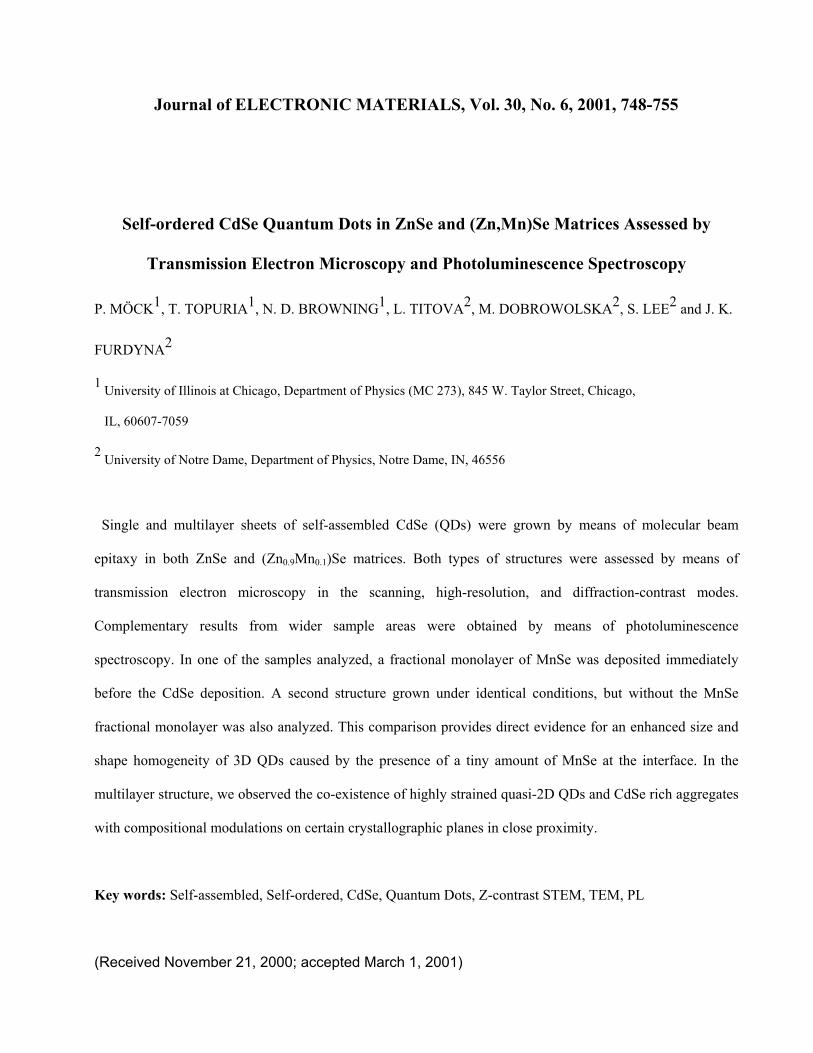
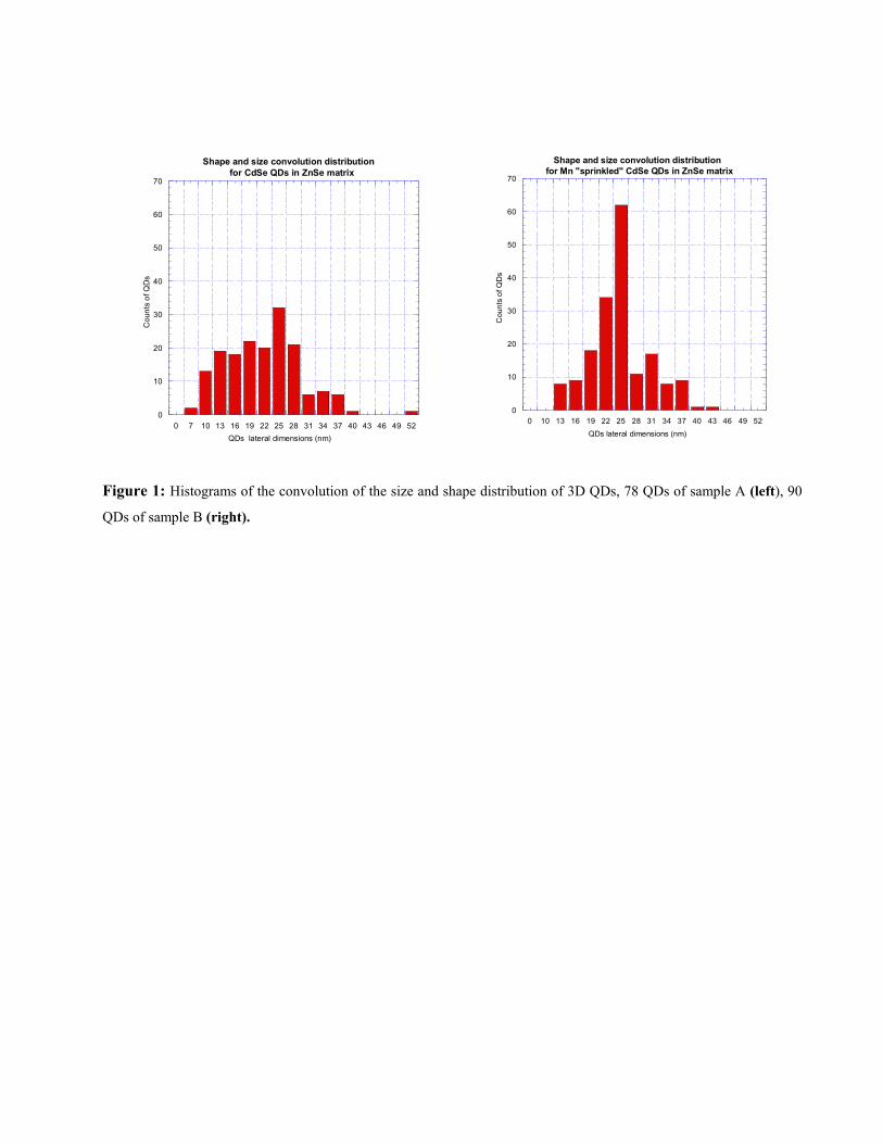
Pronounced inhomogeneities in the shape and size of the QDs were observed for sample A (no Mn
“sprinkling”), as shown by the histogram in Figure 1 (left side). This histogram contains a convolution of the
size and shape of the QDs that was obtained by plotting the largest and smallest lateral dimension as seen in
low-resolution Z-contrast STEM images. Statistical analysis of this data gives an average QD size
(expectation value20) of 22 nm and a standard deviation of 7 nm. Expressed as a relative spread of the QD
base widths (sizes) along the lines of ref.21, we obtain a shape/size “homogeneity” of 32%. The QDs, seen in
both low resolution Z-contrast, Fig. 2b, and bright field images (where the influence of the strain field
surroundings can be suppressed by a suitable choice of the imaging conditions) in STEM, possessed a wide
variety of shapes. On average, the length to width ratio of the elongated QDs was approximately 1.4. There
were, in addition, QDs with shapes of more or less regular rings, pairs of triangles, and dumbbells. About
20% of the QDs were significantly elongated with a ratio of the longer to smaller axis of about 4:1 and were
considered as representing coalesced QDs. Furthermore, orientation order, i.e. the lowest level in the
phenomenological hierarchy of self-ordered QDs arrangements3, was observed at special nucleation sites
such as terrace edges.
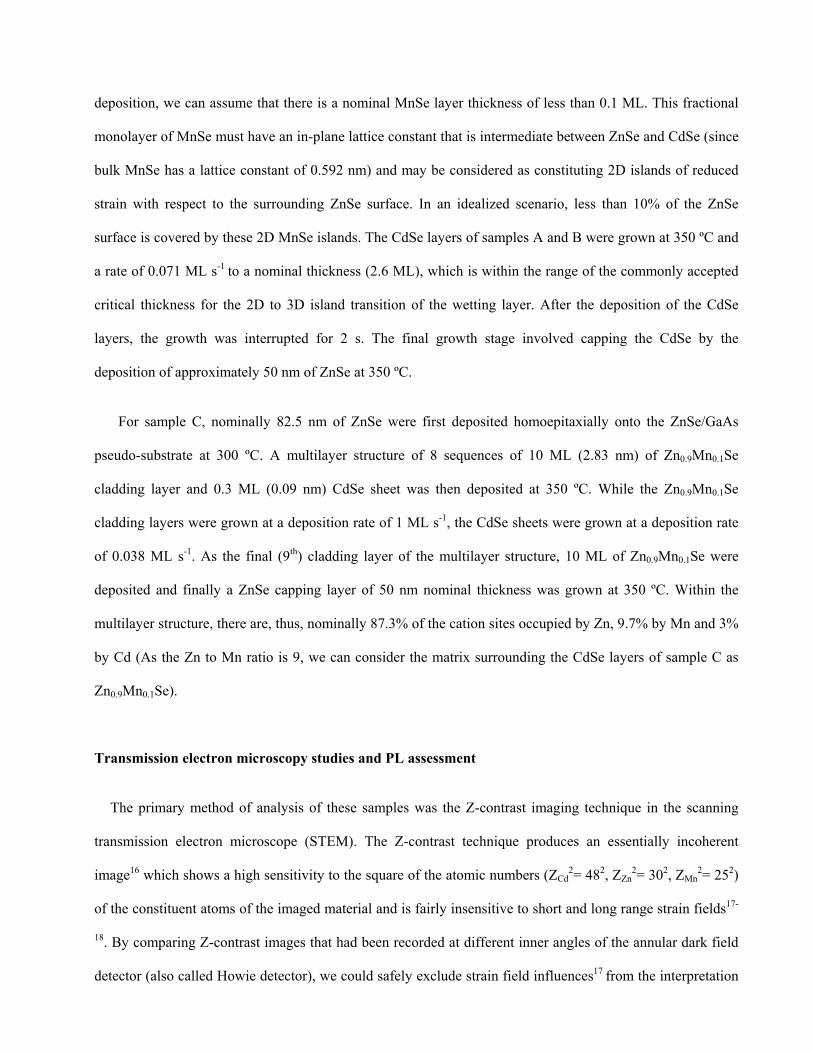
For sample B (with Mn “sprinkling”), a more homogeneous distribution of the shape and size of the QDs
was observed. More or less circular to oval shapes dominated (Figure 3a,b). The smaller QDs of up to
approximately 10 nm diameter were usually more circular. The larger QDs were usually more oval with an
average ratio of the longer to the shorter axis of on average about 1.2 to 1.4. These observations can be
summarized as indications of QDs shape/size order, i.e. the 2nd/3rd levels of the phenomenological hierarchy
of self-ordering processes3. This is well reflected in Figure 1 (right side), where the histogram is again a
convolution of the size and shape distribution. The statistical analysis of the data represented graphically in
Figure 1 (right side) gives an average QD size of 25 nm and a standard deviation of 6 nm. Expressed as a
relative spread of the QDs sizes along the lines of ref.21, we obtain a shape/size “homogeneity” of 24%. This
Page 7
is still more than twice the value that has been achieved for the size “homogeneity” of InAs QDs in GaAs
matrices21, but a remarkable improvement over sample A. The average QDs size has also increased slightly
due to the influence of the deposition of a fractional ML of MnSe.
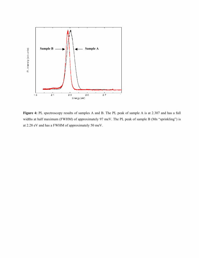
The structural observations from both samples can be correlated to the PL spectra, Figure 4. The PL peak of
sample B is narrower and at an energy that is approximately 0.027 eV lower than the PL peak of sample A.
Our standard interpretation of a narrower PL peak at a slightly lower emission energy around 2.3 eV is that
the shape/size distribution of 3D QDs is more homogenous and that the QDs are slightly larger and/or contain
more Cd22.
An improved shape and size homogeneity, i.e. higher levels of self-ordering in other words, has been
observed before in 3D InP islands on (Ga,In)P, which was lattice matched to GaAs, as a result of the
deposition of a GaP layer in the ML range23. As in our case, the formation of smaller and less isotropically
shaped 3D islands was suppressed in favor of the formation of larger and more isotropically shaped 3D
islands. The effect was explained by static strain considerations24 and a smoothening effect that may have
delayed the formation of the 3D QDs. We suspect that both of these explanations are insufficient and are
currently working on alternatives. Another conclusion to be drawn from our comparison of samples A and B
is: as in the case of InSb islands on GaSb, GaSb islands on GaAs, and InSb QDs in GaSb matrices before25,
the phenomenological model of the hierarchy of self-ordering processes3 has been proven to be applicable to
self-assembled semiconductor QDs.
Controlling the number density value and homogeneity of 3D QDs by Mn “sprinkling”
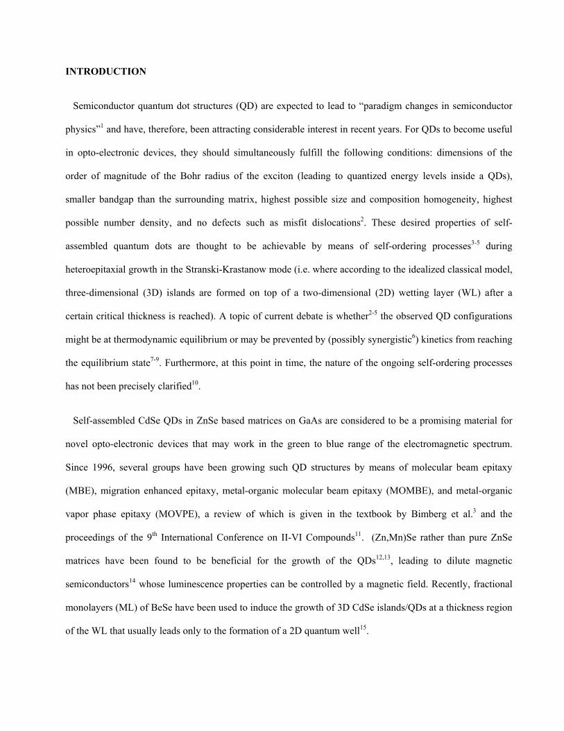
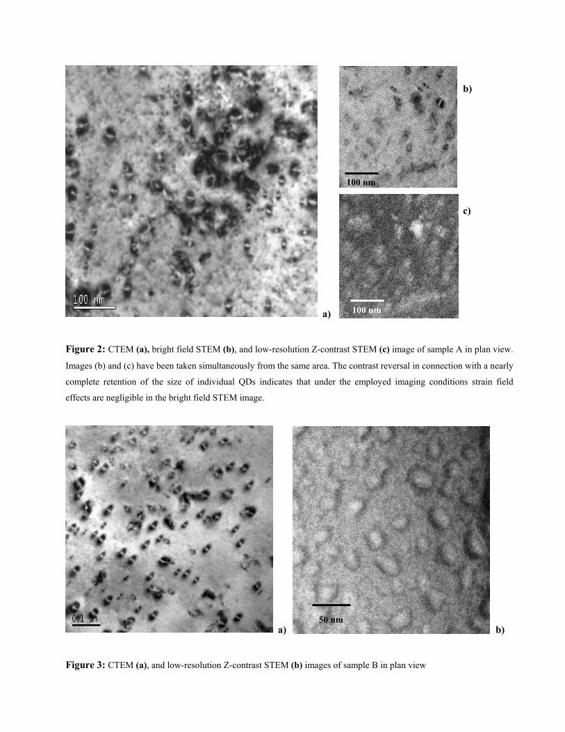
CTEM and low-resolution Z-contrast STEM shown in Figures 2a,b, reveal a rather inhomogeneous
distribution of the number density of the 3D QDs for sample A (no Mn “sprinkling”). Areas with number
densities of up to about 2x1010 cm-2 co-existed with areas where the 3D QDs number density was only about
1010 cm-2. Based on the observation that there are approximately two times more low number density areas
than high-density areas, we estimate an average number density of about 1.3x1010 cm-2. On another TEM
Page 8
specimen of sample A, there were, however, hardly any 3D QDs visible. The above given figures for the 3D
QDs number density may, therefore, not be representative for the whole of sample A. However, what is clear
from the results is that there is an inhomogeneous distribution of 3D QDs on this sample.
For sample B, areas with number densities of up to about 2.2x1010 cm-2 coexisted with areas where the
3D QDs number density was down to about 1.3x1010 cm-2, yielding an average number density of about (1.8 ±
0.5)x1010 cm-2. The number density of 3D QDs was, thus, not only slightly higher as the a result of the
deposition of less than 0.1 ML of MnSe prior to the deposition of the CdSe, but also more homogenous. This
may be partly explained by the nominal thickness of the CdSe layer, which may at certain parts of the sample
be above the critical thickness and at certain other parts below it. In addition, it is conceivable that a
fractional ML of MnSe has similar influences on the self-ordering processes to a fractional ML of BeTe15,
although the static strain relations are reversed since bulk BeTe has a 9.4% smaller lattice constant than ZnSe.
As observed in other semiconductor QDs systems before25,26, a higher number density leads for 3D CdSe
QDs in ZnSe matrix to higher levels in the self-ordering hierarchy.
Further structural differences due to Mn “sprinkling”
Since the Bohr radius of the exciton in CdSe is about 5 nm15, all of the QDs described above cannot be
considered as “true” QDs in the sense of the definition given in the introduction. There is however, some
spatial confinement due to their size which justifies the description as 3D QDs. The strained state of the vast
majority of the 3D QDs in both samples could be inferred from the existence of strain contrast in the CTEM
images shown in figures 2a and 3a.
For both samples, we observed smaller quasi-2D QDs of lateral dimensions of the order of magnitude of
about 5 nm in dark-field CTEM images with a number density in the 1011 cm-2 range for sample A (no Mn
“sprinkling”) and the 1010 cm-2 range for sample B. The high number density of these tiny QDs in sample A
explains the somewhat speckled contrast in Fig. 2a. This type of QDs, however, does not discernibly
contribute to the PL spectra shown in Fig. 4, as it has been shown earlier to photo-luminesce at energies of
Page 9
around 2.4 – 2.7 eV27,28. The lower number density of quasi-2D QDs in sample B may also be explained as
being a result of the deposition of the fractional ML of MnSe. As the formation of 3D QDs probably proceed
in competition with the formation of quasi-2D QDs, a higher number density of 3D QDs may have been
achieved by kinetic processes on expense of the number density of the quasi-2D QDs.
The 3D nature of the QD structures
Employing a nominal electron probe size of 0.5 nm, EDXS spectra were taken for sample B from two
typical QDs and their surrounding areas. In order to improve X-ray quantum counting statistics, analysis
times of several hours were employed. An enhanced Cd concentration with respect to the surroundings of
about 20% was observed at the positions of the QDs. This was also consistent with estimations of the local
Cd-concentration differences from high resolution Z-contrast images. We interpret these results mainly as
projection effects and, thus, as proof of the 3D nature of the typical QDs shown in Figure 2a,b (although there
may also be differences in the Cd composition of the 3D QDs and the remains of the WL). For sample B, a
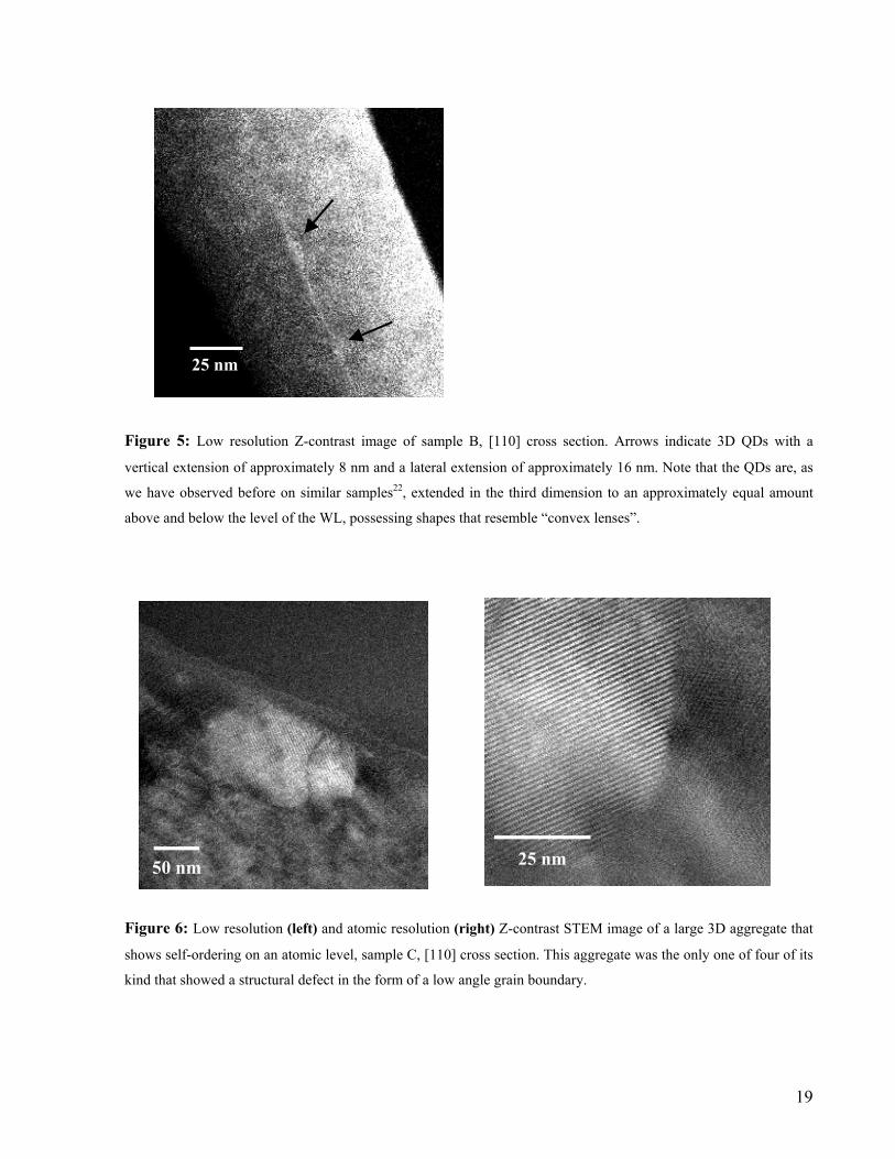
low resolution Z-contrast assessment of a [110] cross section specimen also confirms the 3D nature of the
QDs (Figure 5).
QDs and compositional modulations in the nominal (Cd,Mn,Zn)Se multilayer structure
For the Cd0.03Mn0.097Zn0.873Se multi-layer sample (C), the co-existence of different types of CdSe rich
aggregates in close proximity was observed. The first of these aggregates were easily recognizable by their
pronounced strain fields in cross section HRTEM images. The lateral dimension of these aggregates was of
the order of magnitude 5 nm and this type of QDs may be considered as being quasi-2D. Much larger CdSe
rich aggregates of predominantly the order of magnitude 100 - 200 nm lateral and 50 - 100 nm vertical
represent the second type. Some of these aggregates showed more or less well developed facets in low and
atomic-resolution Z-contrast images and were, despite their large size, usually free of structural defects
Page 10
(Figure 6). Intriguingly, the contrast in the image indicates that there is a compositional ordering taking place
in every second lattice plane of the structure.
Based on Fourier transforms of areas of the order of magnitude 100 nm2 from the aggregate and its
surrounding matrix in Fig. 6 (right side), we interpret the atomic arrangement as compositional modulation on
successive ± (1-10) planes. Self-ordering of such and other kinds has been observed before in ternary and
quaternary alloys of various III-V29,30 and II-VI31 compound semiconductors which belong in their binary
forms to the sphalerite structure type. We consider, here, the Zn and Mn atoms as distributed spatially
randomly, but in a numerical relation of 9 to 1 over their respective ± (1-10) cation site super-lattice planes
and Cd as a second type of atomic species which occupies only its proper positions in alternating ± (1-10)
cation site super-lattice planes. This implies an aggregate composition of about Cd0.5Mn0.056Zn0.444Se
surrounded by a matrix of Mn0.1Zn0.9Se. Our interpretation is confirmed within an accuracy of approximately
20% by a quantitative analysis of the atomic resolution Z-contrast images along the lines of ref.18. Selected
area THEED patterns also confirm this interpretation qualitatively.
A rather isotropically shaped smaller aggregate of the order of magnitude 25 nm was observed in HRTEM
to be free of structural defects and did not possess a noticeable strain field. The analysis of the Fourier
transform of this aggregate and its surrounding matrix indicated an ordering in successive ± (-111) planes, the
also present ± ½ (-113) extra spots probably being due to double diffraction effects. Its composition is likely
to be Cd0.5Mn0.056Zn0.444Se as well, effectively constituting a 3D QD with a compositional modulation inside.
Aggregates of different compositional modulation and with sizes of the order of magnitude 5 nm were also
observed. The related selected area THEED patterns showed ± (½ -½ ½), ± (-½ ½ ½), ± (½ -½ 3/2), ± (3/2 -½
½), ± (-1 1 0), ± (0 -3/2 3/2), ± (2/3 -2/3 0), ± (1/3 -1/3 1) reflections indicating that there are, in addition to the
well known cation ordering on {111} and {110} planes, atomic arrangements in close spatial proximity that
have not been reported before in the literature.
It is noticeable that this (Cd,Mn,Zn)Se multilayer structure was grown with the intention of producing
vertically ordered arrays of quasi-2D CdSe QDs. At present, we cannot explain why aggregates with different
Page 11
types of self-ordered atomic arrangements have been formed in addition to the quasi-2D QDs we intended to
grow. If the self-ordering processes during Stranski-Krastanow growth were, however, of a dissipative10
nature, the co-existence of aggregates with different atomic arrangements and strain status would be a quite
common phenomenon. Further experimental data from III-V and II-VI compound semiconductor QDs
systems appears to support this and is presented elswhere32,33.
SUMMARY and CONCLUSION
Summarizing the results on the single sheet CdSe structures, we have shown that depositing a tiny
amount of MnSe before the deposition of the CdSe layers (which order themselves into 3D QDs
approximately 25 nm in size) leads to a significant improvement of the shape and size homogeneity and
higher hierarchy levels of the self-ordered arrangement. This is reflected by a narrower PL peak from these
QDs. Summarizing the preliminary results on the multilayer (Cd,Mn,Zn)Se structure, we observed the co-
existence of the following CdSe rich aggregates: small (order of magnitude 5 nm, quasi 2D), highly strained
QDs, very large (order of magnitude 100 nm) compositionally modulated aggregates, negligibly strained
compositional modulated aggregates of the order of magnitude of typical 3D QDs, and small (order of
magnitude 5 nm) aggregates with crystallographically different compositional modulation. We conclude that
self-ordering processes of CdSe QDs show a much richer phenomenology that the classical Stranski-
Krastanow growth model accounts for and may, therefore, be of a dissipative nature.
ACKNOWLEDGMENTS
The authors are grateful to Dr. Alan Nicholls from the Electron Microscopy Service, Research Resources
Center of the University of Illinois at Chicago, for experimental support during the electron microscopical
investigations. PM ad TT were supported by the National Science foundation project no DMR-9733895.
Page 12
REFERENCES
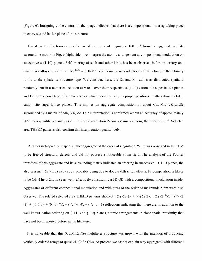
1. D. Bimberg, Semiconductors 33, 951 (1999).
2. N.N. Ledentsov, V.M Ustinov, V.A. Shchukin, V.A. Kop’ev, Zh.I. Alferov and D. Bimberg,
Semiconductors 32, 343 (1998).
3. D. Bimberg, M. Grundmann and N.N. Ledentsov, Quantum Dot Heterostructures, John Wiley & Sons,
1999, Chichester, New York, Weinheim, Brisbane, Singapore, Toronto.
4. V.A. Shchukin and D. Bimberg, Rev. Mod. Phys. 71, 1125 (1999).
5. R.A. Budiman and H.E. Ruda, J. Appl. Phys. 88, 4586 (2000).
6. R. Heitz, T.R. Ramachandran, A. Kalburge, Q. Xie, I. Mukhametzhanov, P. Chen and A. Madhukar, Phys.
Rev. Lett. 78, 4071 (1997).
7. A.-L. Barabási, Appl. Phys. Lett. 70, 2565 (1997).
8. A. Madhukar, Q. Xie, P. Chen and A. Konkar, Appl. Phys. Lett. 64, 2727 (1994).
9. D.E. Jesson, G. Chen, K.M. Chan and S.J. Pennycook, Phys. Rev. Lett. 5156 (1998).
10. Self-ordering processes can be either conservative or dissipative. An example for conservative self-
ordering is the formation of crystalline structures with low energy content at moderately low temperatures. It
seems to be arguable weather or not the processes that lead to the formation of semiconductor QDs in certain
Page 13
II-VI and III-V compound semiconductor systems may be classified as belonging to the conservative self-
ordering type since they show a very rich phenomenology, e.g. ref.6, which depends critically on the growth
conditions.
11. Proc. 9th International Conference on II-VI Compounds, Kyoto, Japan, 1-5 November 1999, eds. I.
Suemune and A. Ishibashi, J. Cryst. Growth 214/215, 1 - 1189 (2000).
12. S.H. Xin, P.D. Wang, A. Yin, C. Kim, M. Dobrowolska, J.M. Merz and J.K. Furdyna, Appl. Phys. Lett.
69, 3884 (1996).
13. C.S. Kim, M. Kim, S. Lee, J. Kossut, J.K. Furdyna and M. Dobrowolska, J. Cryst. Growth 214/215, 395
(2000).
14. J.K. Furdyna, J. Vac. Sci. Technol. A4, 2002 (1986).
15. M. Keim. M. Korn, F. Bensing, A. Waag, G. Landwehr, S.V. Ivanov, S.V. Sorokin, A.A. Sitnikova, T.V.
Shubina and A.A. Toropov, J. Cryst. Growth 214/215, 684 (2000).
16. P.D. Nellist and S.J. Pennycook, Ultramicroscopy 78, 111 (1999).
17. S.J. Pennycook, M.F. Chrisholm, Y. Yan, G. Duscher and S.T. Pantelides, Physica B, 273 (1999).
18. S.J. Pennycook, S.D. Berger, R.J. Culbertson, Journal of Microscopy 144, 229 (1986).
19. S. Lee, I. Daruka, C.S. Kim, A.-L. Barabási, J.L. Merz and J.K. Furdyna, Phys. Rev. Lett 81, 3279 (1998).
20. D.J. Hudson, Statistics, Lectures on Elementary Statistics and Probabilities, Geneva 1964.
Page 14
21. D. Bimberg, M. Grundmann and N.N. Ledentsov, MRS Bulletin, February, p. 31-34 (1998).
22. C.S. Kim, M. Kim, J.K. Furdyna, M. Dobrowolska, S. Lee, H. Rho, L.M. Smith, H.E. Jackson, E.M.
James, Y. Xin and N.D. Browning, Phys. Rev. Lett. 85, 1124 (2000).
23. N. Carlsson, K. Georgsson, L. Montelius, L. Samuelson, W. Seifert and R. Wallenberg, J. Cryst. Growth
156, 23 (1995).
24. In order to explain the observed effects, it was suggested in ref.23 that the very thin GaP layer may,
although pseudo-morphologically strained, lead to partial strain compensation since bulk GaP has a 3.6 %
smaller lattice constant than (Ga,In)P when it is lattice matched to GaAs. Bulk InP, finally, has a 3.8 % larger
lattice constant than GaAs.
We suspect, however, that static strain considerations may not be sufficient in the above mentioned case23
nor in the presented case of the influence of a fractional monolayer of MnSe on the formation of 3D CdSe
QDs, where the strain relations are qualitatively different. Alternatively, we suggest that the self-ordering
processes that lead to an improved size and shape homogeneity of 3D CdSe and InP QDs may be of a
dissipative nature10 and, therefore, be more successfully described by a dynamic synergistic approach (as
already called for by other authors in 19976) - which we are going to outline in forthcoming papers.
25. P. Möck, G.R. Booker, N.J. Mason, E. Alphandéry and R.J. Nicholas, IEE Proc.-Optoelectron. 147, 209
(2000).
26. M. Schmidbauer, Th. Wiebach, H. Raidt, M. Hanke, R. Köhler and H. Wawra, Phys. Rev. B 58, 10523
(1998).
Page 15
27. D. Schikora, S. Schwedhelm, D.J. As, K. Lischka, D. Litvinov, A. Rosenauer, D. Gerthsen, M.
Strassburg, A. Hoffmann and D. Bimberg, Appl. Phys. Lett. 76, 418 (2000).
28. M. Strassburg, Th. Deniozou, A. Hoffmann, R. Heitz, U.W. Pohl, D. Bimberg, D. Litvinov, A.
Rosenauer, D. Gerthsen, S. Schwedhelm, K. Lischka and D. Schikora, Appl. Phys. Lett. 76, 685 (2000).
29. J.Y. Tsao, Materials Fundamentals of Molecular Beam Epitaxy, Academic Press, Inc., 1993, Boston, San
Diego, New York, London Sydney, Tokyo, Toronto; chapter 4, pp. 93 - 150.
30. A. Zunger and S. Mahajan, Atomic ordering and phase separation in epitaxial III-V alloys, in Handbook
on Semiconductors, Completely Revised Edition, Elsevier Science B.V., 1994, North-Holland, Amsterdam,
London, New York, Tokyo, Vol. 3B, chapter 19, pp. 1399 - 1514, Ed. T.S. Moss, Volume Ed. S. Mahajan.
31. K. Park, L. Salamaca-Riba and B.T. Jonker, Appl. Phys. Lett. 61, 2302 (1992).
32. P. Möck, T. Topuria, N.D. Browning, G.R. Booker, N.J. Mason, R.J. Nicholas. L.V. Titova, M.
Dobrowolska, S. Lee, and J.K. Furdyna, Mater. Res. Soc. Symp. Vol. 640, P6.3.1 (2000), accessible to MRS
members at http://www.mrs.org/publications/epubs/proceedings/fall2000/
33. P. Möck, T. Topuria, N.D. Browning, G.R. Booker, N.J. Mason, R.J. Nicholas. L.V. Titova, M.
Dobrowolska, S. Lee, and J.K. Furdyna, Proc. 6th International Symposium on Advanced Physical Fields,
“Growth of Well-defined Nanostructures”, 6th – 9th March, 2001, National Institute for Materials Science,
Tsukuba, Japan.
Page 16
0
10
20
30
40
50
60
70
0 10 13 16 19 22 25 28 31 34 37 40 43 46 49 52
Shape and size convolution distribution for Mn "sprinkled" CdSe QDs in ZnSe matrix
Cou
nts
of Q
Ds
QDs lateral dimensions (nm)
0
10
20
30
40
50
60
70
0 7 10 13 16 19 22 25 28 31 34 37 40 43 46 49 52
Shape and size convolution distribution for CdSe QDs in ZnSe matrix
Cou
nts
of Q
Ds
QDs lateral dimensions (nm)
Figure 1: Histograms of the convolution of the size and shape distribution of 3D QDs, 78 QDs of sample A (left), 90
QDs of sample B (right).
Page 17
a)
100 nm
b)
100 nm
c)
Figure 2: CTEM (a), bright field STEM (b), and low-resolution Z-contrast STEM (c) image of sample A in plan view.
Images (b) and (c) have been taken simultaneously from the same area. The contrast reversal in connection with a nearly
complete retention of the size of individual QDs indicates that under the employed imaging conditions strain field
effects are negligible in the bright field STEM image.
a) b) 50 nm
Figure 3: CTEM (a), and low-resolution Z-contrast STEM (b) images of sample B in plan view
Page 18
Sample B Sample A
Figure 4: PL spectroscopy results of samples A and B. The PL peak of sample A is at 2.307 and has a full
widths at half maximum (FWHM) of approximately 97 meV. The PL peak of sample B (Mn “sprinkling”) is
at 2.28 eV and has a FWHM of approximately 50 meV.
Page 19
25 nm
Figure 5: Low resolution Z-contrast image of sample B, [110] cross section. Arrows indicate 3D QDs with a
vertical extension of approximately 8 nm and a lateral extension of approximately 16 nm. Note that the QDs are, as
we have observed before on similar samples22, extended in the third dimension to an approximately equal amount
above and below the level of the WL, possessing shapes that resemble “convex lenses”.
25 nm
50 nm
Figure 6: Low resolution (left) and atomic resolution (right) Z-contrast STEM image of a large 3D aggregate that
shows self-ordering on an atomic level, sample C, [110] cross section. This aggregate was the only one of four of its
kind that showed a structural defect in the form of a low angle grain boundary.
19