Page 1
INVITED PAPER
Semiconducting large bandgap oxides as potential thermoelectricmaterials for high-temperature power generation?
M. Backhaus-Ricoult • J. Rustad • L. Moore •
C. Smith • J. Brown
Received: 24 April 2014 / Accepted: 12 May 2014 / Published online: 25 June 2014
� Springer-Verlag Berlin Heidelberg 2014
Abstract Semiconducting large bandgap oxides are con-
sidered as interesting candidates for high-temperature
thermoelectric power generation (700–1,200 �C) due to
their stability, lack of toxicity and low cost, but so far they
have not reached sufficient performance for extended
application. In this review, we summarize recent progress on
thermoelectric oxides, analyze concepts for tuning semi-
conductor thermoelectric properties with view of their
applicability to oxides and determine key drivers and limi-
tations for electrical and thermal transport properties in
oxides based on our own experimental work and literature
results. For our experimental assessment, we have selected
representative multicomponent oxides that range from
materials with highly symmetric crystal structure (SrTiO3
perovskite) over oxides with large densities of planar crys-
tallographic defects (TinO2n-1 Magneli phases with a single
type of shear plane, NbOx block structures with intersecting
shear planes and WO3-x with more defective block and
channel structures) to layered superstructures (Ca3Co4O9
and double perovskites) and also include a wide range of
their composites with a variety of second phases. Crystal-
lographic or microstructural features of these oxides are in
0.3–2 nm size range, so that oxide phonons can efficiently
interact with them. We explore in our experiments the
effects of doping, grain size, crystallographic defects,
superstructures, second phases, texturing and (to a limited
extend) processing on electric conductivity, Seebeck coef-
ficient, thermal conductivity and figure of merit. Jonker and
lattice-versus-electrical conductivity plots are used to
compare specific materials and material families and extract
levers for future improvement of oxide thermoelectrics. We
show in our work that oxygen vacancy doping (reduction) is
a more powerful driver for improving the power factor for
SrTiO3, TiO2 and NbOx than heterovalent doping. Based on
our Seebeck-conductivity plots, we derived a set of highest
achievable power factors. We met these best values in our
own experiments for our titanium oxide- and niobium oxide-
based materials. For strontium titanate-based materials, the
estimated highest power factor was not reached; further
material improvement is possible and can be reached for
materials with higher carrier densities. Our results show that
periodic crystallographic defects and superstructures are
most efficient in reducing the lattice thermal conductivity in
oxides, followed by hetero- and homovalent doping. Due to
the small phonon mean free path in oxides, grain boundary
scattering in nanoceramics or materials with nanodisper-
sions is much less efficient. We investigated the impact of
texturing in Ca3Co4O9 ceramics on thermoelectric perfor-
mance; we did not find any improvement in the overall in-
plane performance of a textured ceramic compared to the
corresponding random ceramic.
1 Introduction
1.1 Potential value of oxides compared to other
thermoelectric materials: common advantages
and disadvantages
Thermoelectric power generators convert thermal energy
into electrical energy. Compared to other power generators,
they do not emit toxic gases, have long lifetime, low
operation and maintenance cost and can operate with waste
heat. Due to worldwide concerns about the increasing
demand of energy supply, limited availability of fossil fuel,
M. Backhaus-Ricoult (&) � J. Rustad � L. Moore � C. Smith �J. Brown
Corning Incorporated, Corning, NY 14831, USA
e-mail: [email protected]
123
Appl. Phys. A (2014) 116:433–470
DOI 10.1007/s00339-014-8515-z
Page 2
impact of global warming, CO2 emission and human
health, green sources of energy become increasingly
attractive solutions. Thermoelectric power generation is
one option. Possible applications include recovery of waste
heat from industrial processes, power plants, incinerators,
melting furnaces, gas heaters, engine exhaust streams and
many others.
Let us consider the example of heat extraction from the
automotive exhaust gas: Currently, only roughly one-third
of the fuel energy is used for the translation of the car; one-
third leaves the car in the form of exhaust gas heat and one-
third heats the radiator fluid. Thermoelectric generators in
the EGR loop, in the exhaust stream after the exhaust gas
after-treatment system (DOC, DPF) or, closer to the
engine, directly at the exhaust manifold or on the engine
surface itself, are considered as a promising technology
that can contribute to lower fuel consumption and decrease
CO2 emission.
The conversion of thermal into electrical energy in
thermoelectric generators is based on the Seebeck
effect: If a semiconductor is exposed to a temperature
gradient, the temperature dependency of its carrier
concentration produces a potential difference across the
material that is proportional to the temperature differ-
ence. Suitable thermoelectric materials produce a large
thermopower (potential difference across the sample)
when exposed to a temperature gradient. They typically
show a strong dependency of their carrier concentration
on temperature and have high carrier density, high
carrier mobility and a low thermal conductivity. Pure
p-type (n-type) materials have only positive (negative)
mobile charge carriers, electron holes (electrons) and a
positive (negative) Seebeck coefficient. Most materials
have both, positive and negative charge carriers, and
may also have in addition ionic charge carriers, so that
the sign of the Seebeck coefficient depends on the
predominant carrier.
The thermoelectric conversion efficiency of a thermo-
electric generator depends on the figure of merit ZT of its
material
ZT ¼ TS2r=j ¼ TPF=j; ð1Þ
with T being temperature, S Seebeck coefficient or ther-
mopower, r electric conductivity, j thermal conductivity
and PF the power factor [1]. Materials for efficient ther-
moelectric generation should simultaneously exhibit large
S, large r and small j and behave as ‘‘an electron crystal
and a phonon glass.’’ Property optimization for a specific
material is difficult due to the coupling of the properties.
The key properties all depend on the carrier concentration;
electrical and thermal conductivity typically increase with
carrier density, while the Seebeck coefficient decreases
with carrier density. Best thermoelectric performance is
expected for heavily doped semiconductors with carrier
concentrations in the range of 1019–1021 mol-1 [1].
Low thermal conductivity in conjunction with high
electrical conductivity is difficult to achieve since heat is
not only carried via lattice vibrations, but also by the
electronic carriers:
j ¼ je þ jlat; ð2Þ
where the lattice conductivity jlat represents the heat por-
tion of the overall thermal conductivity j that is transported
by phonons and the electrical thermal conductivity je the
fraction associated to electronic carrier transport. Carrier
heat transport is related to electrical conductivity and
temperature by the Wiedemann–Franz law
je ¼ LrT ; ð3Þ
with L being the Lorenz number (L = 2.4 9 10-8 V2/K2
for free electrons) [1].
A thermoelectric device typically includes two types
of semiconducting materials, p- and n-type conductors
that form the n- and p-legs of a device. The equilibrium
carrier concentration in a semiconductor is dependent on
temperature. If a device with its p- and n-legs is placed
in a temperature gradient, the carrier concentrations
differ at the hot and cold side of the legs and lead to a
flow of n- and p-carriers, respectively; for the device
with its combination of n- and p-legs, the heat provided
to the hot side of the device then causes an overall flow
of electrical current through the device and delivers
electrical power. Typical thermoelectric modules are
composed of an assembly of alternating n- and p-legs,
thus requiring both n-type and p-type thermoelectric
materials.
To recover about 20 % of the heat energy in some of the
above mentioned applications, n- and p-materials with a
figure of merit of around 2 are needed [1].
1.2 General summary on thermoelectric material
performance
In the past years, extended research efforts have focused on
the development of thermoelectric materials. Presently
only tellurides have reached broad commercialization.
Bi2Te3-based modules are used as Peltier cooling elements,
in refrigerators or cooled car seats. Bi2Te3/PbTe2 thermo-
electric generators (TEG) are used in prototypes and small
serial productions in cars to recover exhaust gas heat from
the automotive tailpipe. CoSb3-based skutterudites are in
the development for the same application, with the goal to
also handle the higher exhaust temperatures that have to be
filtered out by an over-temperature valve for the telluride
modules. Si–Ge alloys found application in outer space
probes, where nuclear energy is used as heat source, so that
434 M. Backhaus-Ricoult et al.
123
Page 3
electric energy can be produced over extremely long
periods of time (contacts are spring-loaded and modules
operate in constant temperature gradients).
Several low-temperature thermoelectric materials have
been developed. (Pb, Bi,…)(Te,Se,S) tellurides have been
optimized to ZT = 1–1.2 over a broad temperature range
for both, n- and p-type materials and, with silver or thal-
lium substitution, reach even ZT [1.5. Due to chemical
stability restrictions and low-melting point, applications of
Bi2Te3-based materials are limited to low temperature
(\450 �C) and, in addition, require protective surface
coating. Lead telluride has higher-temperature stability, but
is considered as environmentally unfriendly (regulated in
several countries). Limited chemical stability also restricts
applications of clathrates, skutterudites and silicides. Sur-
face protection against oxidation extends application tem-
peratures of skutterudites and silicides to 600–650 �C.
Some high-performance thermoelectric materials have
limited implementation due to environmentally unfriendly
component, such as lead, thallium,… or rare/expensive raw
materials, such as germanium, indium, ruthenium and
others.
Needs for low- and intermediate-temperature applica-
tions are in principle covered by tellurides, skutterudites,
silicides and silicon-based alloys [2, 3], even though fur-
ther material improvement is required to reach high con-
verter efficiencies. However, efficient, low cost,
environmental-friendly thermoelectric materials that can
operate at high temperatures (800–1,000 K) in air are still
lacking. Oxide materials have been considered as promis-
ing candidates based on their larger chemical and tem-
perature stability, their low cost and lack of toxic elements
[4, 5]. The best thermoelectric oxides include Na-interca-
lated Co oxide [6], layered misfit cobaltites, perovskites
[7], ZnO [8], In2O3(ZnO)n [9]. According to the literature,
single crystals of p-type sodium cobaltite excelled in ZT
and reached for optimized composition and orientation ZT
on the order of 1 [6], while ZT remains lower for known
n-materials. Significantly lower ZT values are reported for
polycrystalline materials. Ca3Co4O9 [10], doped SrTiO3
[11] and doped ZnO [8] show promising properties, but
stable polycrystalline materials with reproducible high
performance suitable for large-scale production have not
yet been demonstrated. Compared to other higher-perfor-
mance thermoelectric materials, most semiconducting
oxides suffer low carrier mobility at high carrier concen-
tration. They typically exhibit rather small power factors,
but offer relatively low thermal conductivity. Although
general concepts such as donor doping for enhancing the
carrier concentration are applicable to oxides, independent
tuning of the electrical properties seems to be more difficult
for oxides than for other small bandgap semiconductors. A
similar statement can be made for enhanced phonon
scattering through nanostructure engineering. Despite the
numerous efforts of introducing secondary-phase nano-
particles into oxides, no (reproducible) breakthrough has
been achieved.
2 Scope of this review
Due to their high-temperature stability, lack of toxicity and
low cost, semiconducting oxides are considered as poten-
tial candidates for thermoelectric power generation. Com-
pared to other high-performance thermoelectrics, they offer
low thermal conductivity, but reach only small power
factors as result of low carrier mobility and localized
charge carriers. The aim of this review was to assess the
potential of large bandgap semiconducting oxides by
evaluating existing approaches for tuning their electronic
and thermal properties. A key challenge for all thermo-
electric materials is the strong coupling of the thermo-
electric properties that has to be overcome to reach high
performance. The question is raised if it is more difficult to
overcome this coupling for oxides with their high carrier
density and low carrier mobility.
Doping is a standard procedure for semiconductors to
increase their carrier concentration and can also be applied
to oxides. However, the high carrier densities in semicon-
ducting oxides make effective doping more difficult; we
wonder if effective tuning and band engineering through
doping is possible for oxides and to what extent.
A further challenge in oxide materials becomes visible
when the widely used approach of nanostructured, engi-
neered microstructures is considered for enhancing phonon
scattering and decreasing the thermal conductivity. Struc-
turation at the nanoscale is efficient for materials with
mean free phonon path in the range of 10 nm and more and
can strongly reduce their thermal conductivity. It is more
difficult to match the mean free phonon path in oxide
materials (range of 1–2 nm or less) by microstructural
features of suited size for efficient scattering. We will
analyze and compare in this review the efficiency of pho-
non scattering at point defects, hetero- and homovalent
dopants (alloy scattering), grain boundaries, nanoprecipi-
tates and other nanoscale structures and especially analyze
the efficiency of crystallographic defects, such as stacking
faults, dislocations and point defects and superlattice
structures compared to nanograin size and nanosize sec-
ond-phase precipitates.
For our systematic experimental assessment, we select a
number of representative multicomponent oxides, that
range from materials with simple crystal structure (perov-
skite) to oxides that form planar crystallographic shear
defects (single sets of crystallographic shear planes in
Magneli phases [12] or intersecting shear planes in block
Semiconducting large bandgap oxides 435
123
Page 4
structures or more randomized channel structures), adopt
layered superstructures and/or actively partner with a wide
range of secondary phases in composites. Many of the
selected oxides were chosen because their crystallographic
or microstructure features are within the size range of
0.3–20 nm and thus suited to interact with oxide phonons
in materials. In addition, for many of these oxides, doping
can be used to introduce intergap states so that some tuning
of the materials to higher electric performance seems fea-
sible. We explore the potential of these oxide materials by
studying the effects of doping, grain size, defect engi-
neering, addition of second phases, considering some
aspects of the impact of processing, providing a general
analysis of the figure of merit of these materials and dis-
cussing the expected device performance. We provide a
brief comparison of oxides to other thermoelectrics and
extract the key differences.
3 Concepts for managing thermoelectric properties
and their applicability for oxides
Enhancing the figure of merit of thermoelectric materials is
a key goal in the development of efficient thermoelectric
generators that led to the search for materials with phonon
glass, electron-crystal behavior. Several general approa-
ches have been described and implemented to reach this
aim. They can be roughly divided into measures with focus
on improving the power factor, while preserving (or even
decreasing) the thermal conductivity and approaches for
decreasing the thermal conductivity, while preserving or
even increasing the power factor. Even though the ther-
moelectric properties are highly coupled and no full sepa-
ration of both approaches is possible, this rough
classification helps to organize and review the approaches
implemented so far.
3.1 Concepts for improving the power factor
Doping has turned out to be a very efficient path to higher
power factors in many different semiconducting materials
[1]. Despite a strong coupling of properties, an overall
benefit in the thermoelectric power factor is often achieved
for semiconductors from doping, which leads to an increase
in ZT, since the charge carrier densities and their contri-
bution to the thermal conductivity remain low. The same
concept of increasing the carrier concentration through
doping can be applied to oxides. However, unlike semi-
conductors with their limitation by the carrier concentra-
tion, oxides have relatively high carrier concentrations and
are limited by their low carrier mobility. The question then
has to be asked whether doping is an efficient approach for
oxides. The benefit of an increase in power factor can
easily be annihilated by a substantial increase in thermal
carrier conductivity. High-conductivity oxides would suf-
fer most by increase in thermal conductivity.
Band engineering can be used to reach large power
factors. Based on Vining’s [13] expressions for conduc-
tivity and Seebeck coefficient from the density of states, a
special role can be attributed to states close to the Fermi
level, especially high densities of state in the bandgap just
below the Fermi level. Based on statistical thermodynamics
relationships between the Seebeck coefficient and the
derivative of the DOS at the Fermi level, an anomaly high
Seebeck coefficient is expected for high DOS and large
value for its slope close to the Fermi level. Tuning of the
bandstructure by doping is more efficient for semicon-
ductors than for oxides, since the densities of dopant-
induced intergap states remain very small in oxides.
In case of anisotropic distribution of carriers in a structure,
carrier pockets can be targeted and engineered for best ther-
moelectric property combination. The concept was described
for Si/SiGe and GaAs/AlAs superlattices, where the carrier
distribution was rendered anisotropic in the superlattice
structure [14], but also for anisotropic bulk materials.
Additional states can be introduced in the DOS of a
material through interaction with a dopant or second-phase
particles by a so-called resonance effect and yield to an
increase in Seebeck coefficient. Heremans [15] reported
doubling of ZT of PbTe by doping with thallium; thallium
provided additional energy levels (resonance levels) and
increased the density of states close to the Fermi level,
which then drove a higher Seebeck coefficient. Another
example is the interaction of ErAs nanoprecipitates with a
GaInAs matrix [16].
In nanostructured materials with the correct nanodi-
mensions, low-energy electrons are scattered at the inter-
face barriers, while higher-energy electrons pass unaffected
so that an energy filtering of the electrons takes place. For
the correct combination of nanodimension and electron
energy, the electron density distribution is narrowed by
such scattering in proximity of the Fermi level, so that a
beneficial effect on the Seebeck coefficient can be obtained
[14, 17].
Significant increase in ZT was achieved for low-
dimensional materials, when not only the thermal con-
ductivity was decreased, but also the Seebeck coefficient
increased by quantum confinement and strong localization
of states close to the Fermi level. Introduction of nanosize
alters the density of electronic states by quantum confine-
ment. The discontinuity of the electric properties can lead
to a decoupling of Seebeck coefficient, electrical conduc-
tivity and thermal conductivity and in special configura-
tions increase the figure of merit [14]. Examples are the
layered quantum dot structures of doped PbTe with (PbS-
eTe) dots that reached ZT = 3.5 (570 K) [18].
436 M. Backhaus-Ricoult et al.
123
Page 5
3.2 Concepts for reducing thermal conductivity
Several approaches focus directly on enhanced phonon
scattering to decrease the thermal conductivity.
Amorphous materials or glasses offer lowest thermal
conductivity; however, they do not meet the requirement of
high electrical conductivity for good thermoelectric per-
formance. Quasi-crystalline alloys and conducting glasses
so far have not reached promising performance.
Introduction of homovalent and heterovalent dopants in
the crystal lattice yields enhanced scattering of phonons at
the perturbed lattice sites. The volume fraction of the alloy
scattering centers is limited by the maximum solubility of
the various atoms/ions in the structure. Thus, its contribu-
tion remains often of limited importance for oxide mate-
rials with small solubilities and high carrier concentrations.
Heavy-ion species with large vibrational amplitude
(rattlers) at partially filled structural sites provide efficient
phonon scattering, as can be seen in skutterudites, clath-
rates and other cage structures [19]. In addition, a mixture
of different rattler atoms can be used to reach efficient
scattering in a broader range of the phonon spectrum
(demonstrated in multi-filled skutterudites [20]).
Nanostructured monolithic materials, composites and
superlattices offer a large number of grain boundaries and/
or interfaces that can be designed to reduce the thermal
conductivity more than the electrical conductivity [21].
The mean free path of electrons in solid matter is in general
much shorter than the mean free paths of phonons. In
addition, phonons show a very broad spectrum that for
materials such as silicon can range up to tens of micro-
meters, so that structural and mass perturbations within a
certain length scale range can be created in a crystal to
produce strong scattering of the phonons, but not of the
electrons. In some cases, only the low-energy electrons are
scattered at an interface barrier so that, in the best con-
figuration, energy filtering [14, 17] of the electrons takes
place and a narrower electron density distribution in
proximity of the Fermi level is obtained that then provides
in addition a beneficial effect on the Seebeck coefficient.
Structuration of a material at the nanoscale cannot only
include introduction of nanograins or fine second-phase
dispersions, but also nanopores. Extended efforts on con-
trolling nanovoid size and distribution together with
assessing related changes in thermoelectric performance
have been undertaken for ZnO [22].
Minimization of jlat through efficient nanostructuration
has been proposed as a path to high ZT. Phonon scattering
in nanostructured monolithic and composite materials has
been suggested and successfully implemented for example
for Si-based materials. Si–Ge alloys with grain sizes from
micrometer down to 10 nm have been systematically
studied [23]. Decreasing the grain size into the nanometer
range, adding second-phase particles and amorphous grain
boundary layers have been used to enhance phonon scat-
tering in Si–Ge and shown significant improvement in the
figure of merit due to enhanced phonon scattering at the
grain boundaries in the nanomaterials. The success for Si–
Ge alloys cannot easily be reproduced for other materials
because silicon has a very high lattice conductivity
([10 W/mK at 1,000 K), a huge phonon mean free path of
200–300 nm and an extremely wide distribution in its
phonon energies, ranging from free phonon paths of 3 nm
to a broad tail with more than 10 or even 50 lm. Phonons
of those energies can be efficiently scattered by nanograins
of 100, 200 nm and even larger. Broad grain size distri-
bution in the nanomaterials offers enhanced scattering for
broad phonon distributions.
For the evident reason that most materials have not
similarly large mean free path and broad distribution as
silicon, the nanostructuration approach for enhanced pho-
non scattering was applied with less success other materi-
als, such as tellurides, silicides and skutterudites.
3.3 Potential of renowned concepts of thermoelectric
performance tailoring for oxide materials
Compared to metallic semiconductors, oxides typically
have a larger bandgap, higher carrier density, more local-
ized electrons and much lower carrier mobility. While for
metallic semiconductors the power factor can typically be
improved by increasing the carrier concentration through
doping and this is sufficient to raise the figure of merit, the
high carrier concentrations in conductive oxides make this
approach more difficult and produce a stronger coupling of
electrical conductivity, Seebeck coefficient and thermal
conductivity. Therefore, traditional approaches are less
efficient to increase the figure of merit in large bandgap
semiconducting oxides.
Phonons in oxide materials have a typical mean free path
in the range of 0.2–2 nm, which is about a factor of hundred
smaller than in silicon. In silicon, the phonon distribution
shows a mean free path of 200–300 nm and an extremely
long tail that extends up to tens of micrometers. Therefore,
structural and mass perturbations at length scales from
10 nm to micrometers are able to produce strong phonon
scattering in silicon without having any major impact on the
electrons (at least for large wavelengths). Besides silicon,
very few materials have such large phonon mean free path
and broad distribution. Due to the small phonon mean free
path in oxides, structuration at the scale of 100 nm or even
10 nm, as typically found in nanoceramics or materials with
second-phase dispersions, is not efficient for phonon scat-
tering in oxides. Features of 0.5–2 nm size are needed to
introduce efficient phonon scattering. Features that have
multiple characteristic distances or cover a range are
Semiconducting large bandgap oxides 437
123
Page 6
preferred to a unique size feature, so that a broader frequency
range of phonons can be scattered.
Mass and size fluctuations are introduced in the oxide
crystal lattice by point defects, such as vacancies, homo-
valent and heterovalent dopants in both, cation or anion
sublattices; they offer a suited length scale for scattering
the oxide phonons. However, the volume fraction of such
defects is typically small (\1 % or even\10-3), so that the
number of scattering centers remains relatively small and
the overall benefit limited. Crystallographic defects, such
as dislocations, stacking faults or any other planar defects
also have suited sizes, but again their density has to be high
enough to introduce efficient scattering. Dislocation den-
sities in ceramics remain rather small, even in plastically
heavily deformed materials. Planar defects can occur at
high density in some oxide structures, they include twin-
ning, crystallographic shear, antiphase boundaries. It was
pointed out by Backhaus-Ricoult et al. [24] that crystallo-
graphic shear planes and twin boundaries contribute effi-
ciently to phonon scattering in titania and niobium oxide
ceramics and produce low lattice thermal conductivity.
Layered superstructures offer another opportunity for
enhancing phonon scattering in oxides. It is known that
misfit cobaltites Ca3Co4O9 with their alternating layers of
conducting CoO2- and insulating rock salt units exhibit
anisotropic properties with high electrical conduction in the
plane and low conductivity perpendicular to the plane.
Electrons propagating in the direction of the conducting
layers are less scattered than phonons propagating in this
direction, so that an overall in-plane advantage in the figure
of merit is expected in textured materials.
A comparison of high-temperature lattice thermal con-
ductivities of various oxide materials shows that typical
values range from 3 to 20 W/mK (e.g., 3.5 W/mK for
TiO2, 4–5 W/mK for SrTiO3, 7 W/mK for ZnO, and 20 W/
mK for alumina), while Nb oxide block structures, double
perovskites [25] and misfit cobaltites can show lattice
conductivity below 2 W/mK.
4 Crystallographic shear defects (CS) in large bandgap
oxides
Since crystallographic shear defects play an important role
in several materials of this review, their nature is described
in the following short excursion.
Crystallographic shear occurs in several transition metal
oxides WO3, MoO3, Nb2O5 and the rutile form of titania or
its combination with vanadium, chromium or other oxides
[26]. A crystallographic shear plane is a planar crystallo-
graphic defect that is associated with a change in the anion
to cation ratio without any change in coordination or sig-
nificant deformation of the anion polyhedra surrounding
the metal atoms. The metal coordination polyhedron is
usually an octahedron of oxygen atoms. Oxygen ions are
linked by corners or edges and corners to form a rather
open structure. Upon reduction, either by direct removal of
oxygen or by reaction with lower valence compounds, the
open structure collapses along specific crystallographic
planes, the crystallographic shear planes, to provide lower
energy structures, from which an entire plane of oxygen is
removed. The crystallographic shear vector is equal to an
oxygen–oxygen distance. With the frequency of this so-
called Wadsley defect (or CS defect) in the structure, the
non-stoichiometry can be varied. A homologous series of
defined compounds with different shear plane distances can
be formed. Simple structures exhibit only one set of shear
planes, such as titanium oxide.
Other materials can undergo simultaneously shear on
different planes and form different types of CS defects,
which intersect and result in a block structure. The CS
planes intersect to divide the materials into columns of
corner-linked octahedra. Local rearrangement in block size
and changes in their packing can be introduced by com-
position changes (cation substitution). Defects consisting
of clusters or walls of inappropriate blocks are very com-
mon in these compounds; their occurrence is strongly
controlled by processing.
5 Literature review on large bandgap oxide materials
5.1 SrTiO3
Doped, oxygen-deficient SrTiO3 materials have received
particular attention because of their high Seebeck coeffi-
cients and electrical conductivity [7]. SrTiO3 crystallizes in
the cubic perovskite ABO3 structure with the smaller Ti4?
ions at the cube corners being surrounded by 6O2-,
forming the TiO6 octahedral building units, and the large
Sr2? ions occupying the cube center. Stoichiometric
SrTiO3 is an insulator with a bandgap of 3.2 eV. The
perovskite structure offers some flexibility in composition,
such as oxidation, ultimately leading to the formation of
A2B2O7 pyrochlore, reduction toward A2B2O5 Brown-
millerite, incorporation of AO excess to form Ruddlesden
Popper phases Srn?1TinO3n?1 or integration of BO2 excess
that would ultimately lead to AB2O5 pseudobrookite for-
mation. Intrinsic transport properties of SrTiO3 can be
described by considering Sr-vacancies, O-vacancies and
electronic carriers (Ti-vacancies only have to be considered
at very high temperatures) [27]. Further on, homovalent
and heterovalent substitutions on both, A- and B-sites, as
well as introduction of oxygen vacancies via reduction are
possible. These simple point defects were sufficient to
describe the behavior of SrTiO3 [28]. Substitution,
438 M. Backhaus-Ricoult et al.
123
Page 7
deficiency or excess of the ions in the structure were typ-
ically found to lead not only to chemical and carrier density
changes, but also to structural distortions that lead to sig-
nificant modifications of the band structure. Similar other
oxides, doped n-type SrTiO3 has carrier concentrations in
the range of 1021/mol and low Hall mobility (0.3–0.4 cm2/
Vs), but excels by its exceptionally large effective carrier
mass (m* = 5–10 m0 in Nb-doped SrTiO3, while
m* = 2 m0 in Nb-doped titania and m* = m0 in spinel)
[29]. The large Seebeck coefficient of doped (reduced)
SrTiO3 is a direct result of the large effective mass, the
highly symmetric cubic structure with its triple-degener-
ated t2g state and the high density of states close to the
Fermi level. It results in power factors that are larger than
those of other oxides. The high lattice conductivity of
undoped and doped strontium titanate (5–12 W/mK) is a
disadvantage that is difficult to overcome by nanostruc-
turing for promoted phonon scattering since the phonon
mean free path is in the order of 1–2 nm at 1,000 K. The
amorphous limit of the lattice conductivity is estimated
around 1.8 W/mK (1,000 K).
The layered Ruddlesden Popper phases of the homolo-
gous series (SrO)n?1TinO3n?1 [30] with their superstruc-
tures of n perovskite layers per inserted distorted rock salt-
type SrO layer (also described by removal of TiO2 layers
along (100) and shear of the remaining perovskite block by
1/2[111]) were considered as particularly attractive since
their internal planar defect interspacing promises enhanced
phonon scattering and resulting low lattice conductivity.
Effectively, various Ruddlesden Popper phases were
intensively investigated [31, 32].
5.2 Titanium oxide
We chose titanium oxide as a second model material
family in this review, since it includes not only materials
with a wide range of point defect concentrations (oxygen
vacancies, cation substitution, anion substitution) in
undoped and doped rutile or anatase, but also different
types and densities of planar crystallographic shear
defects and microtwins in its Magneli phases. As a con-
sequence, the titania material family allows us to study
and compare the impact of point defects, planar defects
and grain size on the thermoelectric properties. Scattering
of phonons occurs at the point defects in a crystal and
scales with the concentration of those defects, which can
be impurities, dopant or substitution atoms and randomly
or ordered intrinsic defects, such as oxygen vacancies or
interstitial titanium ions. The TinO2n-x Magneli phases
are particularly interesting for thermoelectric applications
since their crystallographic shear plane distances are in
the same range as the mean free phonon path in these
oxides.
Based on the literature, the Ti–O phase diagram [33, 34]
presents a number of different oxide phases, including
titanium dioxide which crystallizes in three different
structures, rutile, anatase and brookite, the homologous
series of Magneli phases TinO2n-1 with n [ 4, Ti3O4,
Ti2O3, TiO1-x, a number of low-temperature suboxides and
a metallic solution.
At low oxygen activity, titania is an n-type conductor
with oxygen vacancies VO:: and Ti3? interstitials as dom-
inant point defects; the defects are more or less randomly
distributed. Rutile is the thermodynamically stable high-
temperature structure; anatase forms at low temperature
and for small particle size. Rutile has an extended stoi-
chiometry range and is able to host a large number of more
or less randomly distributed oxygen vacancies together
with charge-compensating cations [35]. Point defect mod-
els for rutile have been derived by several authors as
function of oxygen chemical potential, temperature and
doping level [36, 37]. The models indicate that the elec-
trical conductivity of titanium dioxide increases with
decreasing oxygen partial pressure. While donor dopants
improve the conductivity in the donor-controlled interme-
diate oxygen partial pressure range, the highest electrical
conductivities are reached in the extremely reducing
intrinsic regime, where the conductivity is controlled by
Ti3? interstitials and electrons [38]. Random oxygen
vacancies can only accommodate non-stoichiometries up to
x = 10-4 in TiO2-x. Once the oxygen vacancy concen-
tration in the rutile structure exceeds this threshold, the
randomly distributed oxygen vacancies collapse into a
planar shear defect; edge- and face-shared octahedral
replace the corner-shared TiO6-octahedral, and the cation
to anion ratio changes, but the cation coordination and
TiO6 octahedra structure remain unchanged. Crystallo-
graphic shear defects form on (1–21), (12–3),… rutile
planes with shear in the [110] direction. Shear plane type
and density vary, giving rise to a large number of rutile
Magneli phases [39].
The oxygen-deficient Magneli phases TinO2n-1 that
form at very low oxygen activity show CS superstructures
that accommodate the oxygen deficiency through oxygen-
deficient Ti2O3-type crystal slabs that are periodically
inserted every 1, 2,…, n-2 TiO2 layers to form Ti4O7,
Ti5O9,… TinO2n-1 [12]. For the higher Magneli phases
with n = 18–20, the CS densities remain low; the CS
planes are no longer periodically arranged and are strongly
associated with intertwinning. Lower Magneli phases are
reported to exhibit a periodic insertion of their crystallo-
graphic shear planes. Thus, Ti4O7 is built of rutile-like
slabs of TiO6-octahedra that extend infinitely in the a- and
b-directions and that are 4 octahedra thick in the c direction
inbetween the (110)-type shear planes. Ti5O9 shows a
periodicity of five octahedra inbetween the shear planes. In
Semiconducting large bandgap oxides 439
123
Page 8
higher Magneli phases, the energetically most favorable
shear planes typically form first. However, Magneli phases
with n = 4, 5, 6 require very high shear plane densities,
which cannot be provided by the lowest energy planes, so
that energetically less-favorable shear planes with higher-
defect energy form. In the Ti–O system, simultaneous
formation of CS defects on different planes was not
observed.
Shear defects in Magneli phases are separated by 4, 5,
… x d121rutile planes, with interdefect spacings of 0.7–2 nm,
which matches extremely well the mean free path of pho-
nons in titania (about 1 nm), so that a strong phonon
scattering can be expected.
We used literature data [40, 41] and carried out our own
studies [24] for doped rutile, anatase and various undoped
and doped Magneli-phase materials. Improved ZT values
compared to our own results were reported in the literature
for anion-doped Magneli-phase ceramics with nitrogen
Tin(O,N)2n-2 [42] for n [ 15 that showed similar sub-
stantial reduction in thermal conductivity as our own
research on undoped Magneli ceramics, but reached a
slightly higher ZT = 0.25 (1,000 K).
In addition, we compared in our own work the impact of
micrometer and nanometer grain size relative to the impact
of point or planar defects on the thermoelectric properties.
5.3 Niobium oxide
Niobium oxide block structures were included in this
review in the goal of enhancing the CS defect density and
introducing multiple coexisting interdefect distances. Nio-
bium oxides with compositions between NbO2.5 and
NbO2.42 adopt block structures. Two sets of crystallo-
graphic shear planes intersect to divide the materials into
columns of corner-linked octahedral. In projection, the
columns look like rectangular blocks. The phase range of
these structures can be extended by partial substitution of
Nb2O5 by TiO2, which drives the stoichiometry toward
MO2 and introduces additional smaller size blocks, or
WO3, which drives the stoichiometry toward MO3 and
introduces larger size block. Compositional changes occur
at the block periphery. Changes in local composition can
be implemented by local rearrangements in block size and
packing. Defects consisting of clusters or walls of inap-
propriate blocks are very common in these compounds and
are often processing specific. Phase diagram and crystal-
lographic-phase information are provided in [5, 44–46].
Based on the combined information, the niobium–oxygen
phase diagram reveals several oxides, NbO, NbO2, NbO2.5,
the homologous series of structurally related niobium oxide
phases with general formula Nb3n?1O8n-2, n = 5, 6, 7, 8
(Nb16O38, Nb19O46, Nb22O54, Nb25O62), Nb12O29
(12Nb2O5–2O) and Nb94O232 (47Nb2O5–3O).
NbO has a defective NaCl-type structure with both,
ordered cation and anion vacancies, and extends only over
a narrow homogeneity range from NbO0.982 to NbO1.008.
NbO2 crystallizes at room temperature in a deformed
rutile structure with chains of edge-shared NbO-octahedral
along the c axis, while neighboring chains are connected by
shared oxygen atoms. The Nb4? ions are shifted and form
metal–metal pairs within the chains. The bonded Nb–Nb
atoms are separated by a distance of 0.28 nm, whereas the
Nb–Nb distance along the chain is 0.312 nm. Bonding
within chains is reported to be homopolar and expected to
trap all available electrons in these bonds. NbO2 transforms
at about 1,125 K into a basic rutile (The transformation
temperature decreases with decreasing pO2.). NbO2 is a
small polaron conductor. Simple point defect models with
interstitial niobium and niobium vacancies as predominant
defects allow us to describe the intrinsic semiconductor and
metallic conductor behavior.
Nb2O5 is an insulator with a bandgap of 3 eV between
the oxygen 2p-valence band and the Nb 5d� band. It either
adopts a large number of different structures or was
described in the form of slightly different symmetries
[47]. The Nb2O5 structures can be roughly described by
very similar low- and medium-temperature phases that
transform at 1,273 K into a high-temperature block
structure of NbO6 octahedral (3 9 4 and 3 9 5) that share
corners with octahedral in their own block and edges with
octahedral in other blocks. One of the 28 niobium atoms
in each unit cell occupies a tetrahedral site at some block
junction. The low-/medium-temperature unit cell has a
more asymmetric pattern with 42 oxygen atoms forming
large open circles and 8 Nb ions being located in distorted
octahedral, while another 8 Nb ions occupy pentagonal
bipyramids. The remaining 0.8 Nb ions per unit cell are
located in interstitial 9-coordinated sites in the unit cell.
Both stoichiometric phases contain already several types
of niobium ions in the structure; electron densities and
carrier localization are expected to differ for those dif-
ferent niobium sites.
In addition to the stoichiometric phases, numerous
Nb2O5-x phases were reported. Even though no full
agreement on different phases and homologous series was
achieved by the different authors (some due to use of dif-
ferent crystallographic reference systems), most findings
can be summarized as homologous series of structurally
related niobium oxide phases with general formula
Nb3n?1O8n-2, n = 5, 6, 7, 8 (Nb16O38, Nb19O46, Nb22O54,
Nb25O62) and additional oxides of formula Nb12O29
(12Nb2O5–2O) and Nb94O232 (47Nb2O5–3O) [5, 26]. At
least the two latter phases seem to be stable, while others
are described as transient phases that form upon oxidation
of NbO or NbO2. Some of the metastable phases can be
considered as mixtures of different compounds of the
440 M. Backhaus-Ricoult et al.
123
Page 9
homologous series or more complex mixtures of those with
stable compounds. Some structural details are reported
based on HRTEM [30].
Based on high conductivity, tunable structural defects,
wide redox range and extended possibilities for hetero- and
homovalent substitution, niobium oxide-based materials
promise potential as n-type materials for thermoelectric
power generation at high temperature. Since only limited
data on thermoelectric properties are available in the lit-
erature, we investigated the properties of the various nio-
bium oxide phases and the effect of doping, substitution
and second-phase addition [48].
5.4 Tungsten oxide
Oxygen-deficient tungsten oxides were included in our
review, since they form highly defective structures ranging
from defective perovskites over Magneli-type phases to
chain structures. Details of the W–O phase diagram are
reported in [49]. The fully oxidized WO3 phase can be
considered as a modified perovskite-type (ABO3) structure,
where the large A atom is missing and the B atom is W6?.
The W6? atoms occupy the center of the oxygen octahedra.
At room temperature, WO3 is monoclinic rather than cubic
due to tilting of the octahedra. With increasing tempera-
ture, WO3 transforms from monoclinic to orthorhombic
(*603 K) and from orthorhombic to tetragonal
(*1,013 K) with transitions to other tetragonal structures
at higher temperatures. With increasing oxygen deficiency,
two series of Magneli phases are formed, WnO3n-1 and
WnO3n-2. In the WnO3n-1 series, point defects condense to
form crystal shear (CS) planes on {102}, where the lowest
n value is *14. These phases are referred to as {102} CS
phases. In the WnO3n-2 series, the CS planes lie on {103},
n ranges from about 12–28, and they are referred to as
{103} CS phases. For the W oxide Magneli phases, it was
found that each individual Magneli phase WnO2n-1
exhibits only a single n-specific type of shear plane and that
Magneli phase and shear plane change to another type,
when the shear planes get too close and the shear plane
interaction energy becomes too high. At lower oxygen
levels, two additional stable WO3-x phases were found,
W12O34 (WO2.83) and W18O49 (WO2.72). These are not
Magneli phases, rather the octahedra align to form pen-
tagonal columns. They are referred to as PC phases. Below
W18O49, WO2 is the only stable oxide. WO2 has a structure
similar to VO2 and is related to the rutile structure.
5.5 Misfit cobaltites
Even though misfit cobaltites are p-type oxides and do not
fit in the category of the so far considered substoichio-
metric n-type oxide materials of this review, we have
included them to illustrate both, the impact of their
incommensurate layered crystal structure on the thermo-
electric properties and the effect of texturing in case of
anisotropy in the transport properties.
NaxCoO2 [6] was the first metallic oxide with large
Seebeck coefficient that revealed excellent thermoelectric
properties (extrapolated ZT(1,000 K) = 0.7), but unfortu-
nately had a low high-temperature stability (sodium loss at
high temperature and hygroscopic in air). NaxCoO2 is built
of CoO2 layers with sodium atoms inserted inbetween the
layers. Numerous higher misfit cobaltites have been
derived with larger inserted oxide building blocks that are
more stable, such as Ca3Co4O9, BiCa2Co5/3Ox and others.
Ca3Co4O9 [50–52] adopts a CdI2-type crystal structure,
where layers of CoO2 with edge-sharing CoO6 octahedra
alternate with a triple-rock salt layers (Ca,Ca,CoO3). The
two layers have common lattice parameters in the a-
direction of the plane, but different parameters in the b-
direction. They form an incommensurate structure. It is
commonly stated that the CoO2 layers provides directed
planar electrical conduction, whereas the rock salt layers
can be considered as a reservoir for charge injection into
the CoO2 layers. The length scale of the superstructure and
charge transfer can be modified with dopant and substi-
tuting atoms of different sizes.
6 Modeling approaches for predicting thermoelectric
performance of oxides
First principles methods are widely used in the screening
and discovery of new thermoelectric materials, giving a
detailed picture of the band structure and suggesting new
ideas for how to adjust it to optimize thermoelectric per-
formance [53]. A major problem in such applications is the
strongly correlated nature of the electrons in many oxide
materials [54]. In such systems, one-electron theories often
yield limited insight and the many-body aspects of the
electronic structure, ostensibly, have to be explicitly con-
sidered [55]. The electronic structure of strongly correlated
oxide systems, even very simple ones such as TiO2,
remains an active area of research with important impli-
cations in the theory and understanding of oxide thermo-
electric materials. A major question is the extent of
localization of the electrons. If the electrons are delocal-
ized, the transport properties can be estimated from the
band structure, with the band curvature giving the effective
mass. The Boltzmann transport equations can be conve-
niently solved with codes such as BoltzTrap [56] to make
estimates of thermoelectric properties providing informa-
tion such as the optimal doping level for high thermopower
[57]. On the other hand, if the electrons are localized, and
electron transport is dominated by polaron hopping, the
Semiconducting large bandgap oxides 441
123
Page 10
calculation of conductivities requires knowledge of the
hopping matrix elements and reorganization energies. In
such cases, the thermopower can be estimated with simple
statistical mechanical principles.
Computational methods have also been widely applied to
the calculation of thermal conductivities. In comparison with
other simple transport properties, accurate calculation of
thermal conductivities is notoriously difficult and remains an
active area of research, even for simple materials such as
GaN [58]. Because of the long integration times required to
converge the heat–current correlations, even using non-
equilibrium techniques, the methods have only been applied
to systems with empirical potentials and thus have limited
generality. There have not really been sufficient studies
carried out to know how to best construct potential functions
that give accurate conductivities; much of the research effort
still goes into simply computing converged conductivities
(i.e., precision) without worrying too much about accuracy.
The particularly recalcitrant combination of strongly corre-
lated electronic structure and the difficulty of computing
reliable, reproducible thermal conductivities make explora-
tion of thermoelectric materials through molecular modeling
approaches highly challenging.
The TiO2 system illustrates well the inherent difficulties
in searching for optimal dielectric materials using atomistic
modeling approaches. First, the electronic structure of
excess electrons in TiO2 has been a subject of considerable
controversy with contradictory theoretical and experimen-
tal evidence for both localized and delocalized electronic
states. For example, X-ray structural studies in the Ti4O7
(2TiO2–Ti2O3) system have shown evidence for a Verwey-
type transition from localized electronic states at low
temperature to delocalized states at room temperature [59].
This has been recently shown to be consistent with
LDA ? U electronic structure calculations [60]. Recent
calculations [61] have suggested the existence of two
coexisting populations of localized and delocalized elec-
tronic states. In this work, it was shown that, because of the
extremely low mobilities expected for the localized elec-
trons, transport properties should be controlled by the de-
localized electrons.
It is known that there is strong conduction anisotropy in
reduced TiO2 with excess electrons, with high conductivity
along the [001] direction connecting edge-sharing TiO2
octahedra [62]. However, GGA ? U calculations [24] find
negligible anisotropy in the conductivities in contradiction
to experiments. This is an important check on the method;
while absolute conductivities cannot be computed within
the Boltzmann equation without knowledge of the relaxa-
tion time, the extent of anisotropy can still be predicted, at
least under the assumption that the anisotropy in the
relaxation time itself is small. This suggests that the de-
localized picture may not be correct, as it is obvious that a
hopping mechanism will give the expected anisotropy due
to the close Ti–Ti distances along the [001] direction (see
calculations in [63]). On the other hand, Janotti et al. [64]
showed in their Fig. 1 that the effective mass in the [110]
(M) direction is higher than along [001] (Z), a finding that
appears to differ qualitatively from the more complete
analysis provided by BoltzTraP. Further, studies of the
thermopower over the series TiO(1.75–1.91) in Backhaus-
Ricoult et al. [24] give excellent agreement with the Cha-
ikin–Beni expressions for the thermopower expected from
a U0 � kT Hubbard model in the localized-carrier regime
[65]. Presented with such contradictory evidence for a
system-like TiO2-x, it is difficult to see how electronic
structure calculations, at the present time, can serve as a
reliable guide for screening thermoelectric materials in
oxide systems. Clearly the community can look forward to
exciting improvements in computational screening of
thermoelectric oxide materials as research on electronic
structure calculations in strongly correlated oxide systems
moves forward.
Interesting preliminary insights into thermal conductiv-
ity in the TiO2-x system have been provided by molecular
dynamics calculations of thermal conductivity using
empirical potentials [66]. The calculations showed the
expected decrease in conductivity with interplanar spacing
in the Magneli phases; however, they showed an unex-
pected anisotropy with retarded heat conduction along the
Magneli shear planes. The reported effect is small but in
the right sense for improvement of thermoelectric proper-
ties as it is the same direction as the fast direction for
electrical conductivity in Ti4O7 [67]. This finding illus-
trates the promise of atomistic simulation approaches in
designing materials for optimal thermal scattering.
7 Oxide-specific problems and difficulties
for measuring thermoelectric properties at high
temperature
High-temperature electrical conductivity and Seebeck
coefficient have been frequently measured simultaneously
by using a ZEM (Ulvac Technologies) or similar equip-
ment. The thermal conductivity was then measured sepa-
rately. While the Laserflash method was broadly applied
and provided sufficient quality in its heat diffusion mea-
surements, the assessment of heat capacity in the same
equipment was often of low quality and specialized DSC
equipment produced higher-quality heat capacity mea-
surements. The van der Pauw approach allows us to mea-
sure simultaneously electrical and thermal properties on the
same sample; unfortunately, this approach is limited to low
temperatures due to the difficulty of making reliable high-
temperature contacts [1].
442 M. Backhaus-Ricoult et al.
123
Page 11
We used in our work a ZEM3 with platinum electrodes,
carbon contact foil and helium gas with a residual oxygen
content of 5–10 ppm oxygen (0.1 bar total pressure) and
acquired data in the temperature range from 400 to 1,100 K
on plan-parallel polished bar-shaped samples of size
2–3 mm 9 2–3 mm 9 12–15 mm. We restricted our
study to temperatures where the samples were stable during
the measurement time in the ZEM at low oxygen level and
did not change their stoichiometry (reproducible runs).
Stoichiometry changes were observed for some oxide
materials at temperatures [1,000 K or when exposed to
higher (lower) oxygen content than the processing or post-
annealing condition. In our work, we measured thermal
conductivity on carbon-coated 10 mm 9 10 mm 9
2–3 mm samples between 400 and 1,050 K in Argon
(residual oxygen level about 10 ppm) by the laser flash
method in an ANTAR 3. The thermal conductivity j was
derived as product of thermal diffusivity d, specific heat cp
and bulk density q of the sample, j = d � cp � q. The
density of the samples was determined at room temperature
from sample weight and dimensions; thermal expansion
coefficients from the literature were used. Heat capacity
was measured either in a Netzsch DSC 400 or a Laserflash
(Anter), comparing changes to a known standard of alu-
mina (Netzsch) or Pyroceram� (Anter).
In order to extract levers for low thermal conductivity
and compare the measured properties of different materials,
it is useful to derive the lattice thermal conductivities of the
dense materials by extrapolating measured values to full
material density and subtracting the electron contribution
from the thermal conductivity k using the Wiedemann–
Franz law, which is typically well obeyed at high tem-
perature. For lack of better data, we used in our work the
Lorenz number for free electrons 2.45 9 10-8 WX/K2 to
derive our lattice conductivities as function of temperature.
There are some particular challenges for property mea-
surements of oxide materials.
7.1 Effect of oxygen partial pressure and material
relaxation during measurements
Even though it is often stated that thermoelectric oxide
materials offer the advantage of being stable in air, this
statement has to be considered very carefully. Oxides and
especially those which are known for their n- or p-ther-
moelectric performance undergo changes in their oxygen
stoichiometry in their thermodynamic stability range.
Under thermodynamic equilibrium conditions, an oxide
equilibrates with its surrounding oxygen-containing envi-
ronment under oxygen ex- or incorporation. At low tem-
peratures, the kinetics may be sluggish, and a sample may
not be able to respond within the measurement time to a
change in pO2. At high temperature, kinetics may be fast
enough so that a bulk sample may respond rapidly to the
changes in the surrounding environment, particularly to the
oxygen partial pressure, so that a complete bulk sample or
only a surface layer changes its composition. The change in
oxygen stoichiometry corresponds to ‘‘oxygen vacancy
doping’’ and is often used as a powerful driver during the
optimization of oxide thermoelectrics. Therefore, care has
to be taken when thermoelectric properties are measured
for oxide materials, and it has to be evaluated whether the
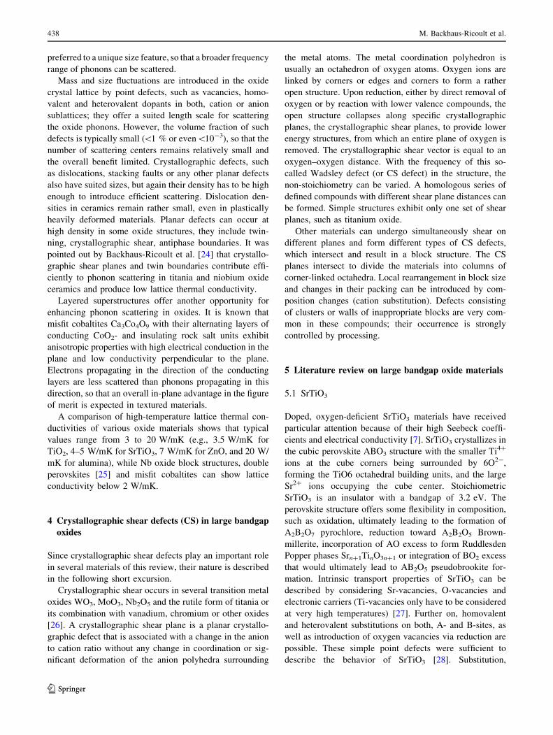
Fig. 1 Schematics of the organization of MO6 octahedral in a perfect
rutile structure (TiO2, NbO2, WO3), b Magneli structure with
crystallographic shear defects on one type of shear plane (homologous
series of TinO2n-1, n = 4–9, …), c block structure with crystallo-
graphic shear defects on intersecting planes. The yellow and blue
squares represent full MO6 octahedral with a central M-atom
symmetrically surrounded by six oxygen atoms. Bonding between
octahaedra occurs via corner-sharing (represented as corner-
connected squares), edge-sharing (represented in the sketch as the
partial overlap of blue and yellow squares which corresponds to the
projected view of edge-sharing octahedral). Additional isolated M
ions are in the block structure (black dots) filling s interblock gaps.
The sketch is obtained by shear on different crystallographic planes
and represents a typical niobium oxide block structure with 3 9 4,
3 9 5, 3 9 3 blocks of NbO6 octahedral
Semiconducting large bandgap oxides 443
123
Page 12
material is ‘‘modified’’ (reduced or oxidized) during the
measurement. It is recommended to run measurements
during heat up and cool down or over long time to identify
material modifications. Often different piece of equipment
are also operated under different atmosphere; for example,
the inert gas ‘‘nitrogen’’ at one site may contain a different
residual oxygen content than the inert nitrogen or argon gas
used at a different site (rough levels of oxygen in bottled
nitrogen or argon are in the ppm range, but depend on the
gas quality).
The example of heavily reduced Zn(Al,Ce)O is used
as illustration. If doped zinc oxide is fabricated at
1,200 �C under heavily reducing environment, and its
electrical properties are measured in argon (5 ppm O2)
environment in a ZEM, during heating, at temperature
around 800 K, the electrical conductivity typically
shows a discontinuity in its slope due to oxidation of the
sample. Conductivity data acquired during sample cool
down will follow the lower conductivity branch of the
oxidized material.
7.2 Effect of material anisotropy in measurements
Many thermoelectric materials have complex (non-cubic)
crystal symmetry and show substantial anisotropy in their
properties. The anisotropy of a material can be further
enhanced by processing; uniaxial pressing, forging, tem-
plating, extrusion, etc., and may introduce anisotropy in
the microstructure and in the pore structure of the mate-
rial so that the electrical and thermal properties of a
sample differ in different sample directions. To assess the
thermoelectric properties of such anisotropic samples or
materials, it is important that electric conductivity, See-
beck coefficient, and thermal conductivity are measured
in the same direction of the sample (and preferentially on
the same sample).
The literature on oxide thermoelectric materials is
unfortunately full of data sets that were not measured in
same direction and show an exaggerated figure of merit.
We will use two examples for illustration, a hot-pressed
porous material with flattened pores in the compression
axis and a layered crystal structure, misfit cobaltite
Ca3Co4O9 with high conductivity in the CoO2 plane and
low conductivity perpendicular to it.
For small hot-pressed disk samples, bar samples are
typically cut from the disk for assessing electrical proper-
ties by ZEM in the direction perpendicular to the pressing
direction, which contains the smaller pore projections and
consequently has higher conductivity. If the disk itself or
part of it is used to assess the thermal transport by the
Laserflash method, the thermal conductivity is measured in
the direction of the compression axis, which means through
sections with large pore projections and thus lower thermal
(and electrical) conductivity. If those two sets of measured
data are combined, the resulting figure of merit is overes-
timated and false:
ZTfalse ¼ T rradSradial=vaxial� �
[ T rradSradial=vradial� �
¼ ZT
By precaution for a new process or material, it is rec-
ommended that measurements are always done in the same
direction or for both directions to assess the anisotropy of
the samples.
The crystalline anisotropy in layered crystal structures,
as for example misfit cobaltites, is praised for its low
thermal conductivity in the direction perpendicular to the
layering and the high electrical conductivity in the direc-
tion of the layer. A clear benefit from the anisotropy in
thermal and electric conduction is not evident. In textured
cobaltite ceramic, the grains are no longer randomly ori-
ented, but preferentially aligned in one direction. The
texturing yields anisotropic properties and makes it nec-
essary to assess thermoelectric material performance from
property measurements in the same directions, see Figs. 24
and 25.
8 Extraction of drivers for oxide thermoelectric
properties from experimental data
The strong coupling of the thermoelectric properties
makes it of little use to evaluate the effect of material
changes on a single thermoelectric property. Instead, the
impact on the overall thermoelectric performance has to
be compared. In order to compare materials and extract
trends in their thermoelectric properties as function of
dopant nature and concentration, grade of reduction,
second-phase addition, etc., we plotted both the Seebeck
coefficient and the lattice thermal conductivity as a
function of the logarithm of the electrical conductivity. In
these plots, our measured properties were extrapolated to
fully dense ceramics. The first type of plot is commonly
known as Jonker plot. Jonker had shown that for non-
degenerate semiconductors with band conduction, the
electrical conductivity (r) and Seebeck coefficient (S) are
related according to the equation:
S ¼ � k
eðln r� ln r0Þ ¼ �2:3026
k
elog r� log r0ð Þ; ð4Þ
where ? is for n-type and - is for p-type semiconductors
[68]. Similar relationships have been formulated for small
polaron conductors [69, 70].
Jonker plot and lattice-versus-electrical conductivity
plot allow us to identify drivers (inhibitors) for thermo-
electric performance. Drivers are found in the high Seebeck
coefficient–high conductivity corner of the Jonker plot with
largest possible deviation from the line representing the
444 M. Backhaus-Ricoult et al.
123
Page 13
ideal semiconductor behavior and in the lattice-versus-
electrical conductivity plot in the corner of high electric
conductivity and small lattice conductivity. If the experi-
mental data of a material family can be described by a
common relationship between S and r, then PF and ZT of
that material family or group of compositions can be cal-
culated from that relationship.
9 Material results
9.1 SrTiO3
9.1.1 Literature results on SrTiO3 thermoelectric
properties
In the field of oxide thermoelectrics, doped, oxygen-defi-
cient SrTiO3 ceramics have received particular attention
because of their high Seebeck coefficient and high electrical
conductivity, although their high thermal conductivity was
an obstacle for the realization of high ZT bulk materials.
Many studies explored the effects of reduction and doping
on the thermoelectric properties of SrTiO3 [4]. In the lit-
erature, results for oxygen vacancy doping [71], heterova-
lent doping [72] and homovalent A-site doping [29] were
reported. Some of the highest ZT values for n-type oxide
bulk materials were reported for Nb-doped strontium tita-
nate: ZT(1,000 K) = 0.35 for SrNb0.2Ti0.8O3 [73]. Efforts
on doping, grain size decrease and second-phase disper-
sions were implemented for enhanced phonon scattering
and led to a variety of materials with ZT(1,000 K) =
0.3–0.35. We demonstrated ZT (1,050 K) = 0.33 in poly-
crystalline bulk materials SrNb0.2Ti0.8O3-d and (La,Y)0.2-
Sr0.8TiO3-d with TiC addition [74]. We also investigated
the effects of combined heterovalent and homovalent A-site
doping (La0.15Y0.05CaxSr0.8-xTiO3-d), A ? B-site co-dop-
ing ((La,Y)xSr1-xNbyTi1-yO3-d), titania excess ((La0.15-
Y0.05Sr0.8)1-yTi1?yO3-d), and different second-phase
additions (TiB2, TiN, NbC, LaB6, LaAlO3, Y3Al5O12) on
the thermoelectric performance of strontium titanate [75,
76]. Although no bulk materials with ZT(1,000 K) values
higher than 0.33 were discovered, we found different paths
for reaching this value and gained insight into drivers and
limitations for further material development.
High thermal conductivity and limited dopant solubility
were key challenges for the successful development of
strontium titanate bulk materials with higher ZT. For thin
films and particularly constrained films on substrates,
higher ZT was reported (ZT = 0.37 for pulsed laser
deposited expitaxial films) [77]; particularly high ZT
(ZT = 2.4) was reported for the two-dimensional interfa-
cial layers between doped SrTiO3 film and LaAlO3 sub-
strate [78].
The layered crystal structures of the Ruddlesden Popper
phases offered another approach for reducing the thermal
conductivity. Effectively, a decrease in lattice conductivity
(about 40–50 % at room temperature and 80–90 % at
1,000 K compared to that of the symmetric perovskite
structure) was found, but it was unfortunately accompanied
by low electrical conductivity. The latter was caused by the
insulating nature of the SrO layers and a small effective
mass, only half of the value in the Nb-doped perovskite
structure. ZT typically ranged only around 0.15–0.2 at
1,000 K.
Several attempts were reported on modeling lattice
vibrations and their impact on thermal and carrier con-
duction [79].
9.1.2 Results from own work
In our own work, we have investigated the effects of
reduction, A-site, B-site and co-doping, as well as second-
phase addition on the high-temperature thermoelectric
properties of strontium titanate materials.
Processing We derived strontium titanium oxide materi-
als from mixtures of SrCO3, La2O3, Y2O3, TiO2, Ti2O3
and, in some cases, additional CaCO3 or Nb2O5 powders
that were turbula-mixed, cold-pressed into pellets, calcined
at 1,200 �C for 12 h in air, milled, then recalcined under
the same conditions and re-milled. For some materials, fine
second-phase particles of TiC, TiN, TiB2, LaB6, Al2O3 or
zirconia were added. Cold-pressed pellets were reduced in
a graphite bed at 1,400 �C for 6 h. The reduced materials
were milled and sieved to -325 mesh. Powders were
densified in a graphite die by current-assisted rapid sin-
tering (SPS) with hold at top temperature 1,500 �C for 15 s
under 35 MPa. Reduction of the materials was induced by
heat treating the powders in a graphite bed and, in some
cases, was enforced by adding reducing second phases.
9.1.2.1 Oxygen vacancy doping Reduction, also known
as oxygen vacancy doping, is a key driver for the ther-
moelectric properties of strontium titanate; high electrical
conductivity is only achieved in highly reduced materials.
Intrinsic (unreduced) SrTiO3 ceramics have very low
electrical conductivity and large Seebeck coefficient,
associated with a thermal conductivity in the range of
6–8 W/mK, so that their figure of merit remains below
ZT(1,000 K) = 0.01. Donor doping with La or Nb leads to
unreduced materials with Seebeck coefficients of -250 to
-500 lV/K and electrical conductivities that roughly scale
with the level of dopant and range from 2,000 to 8,000 S/m
at 1,000 K. Even highest concentrations of donor dopant,
for example 27 % of niobium, still do not provide prom-
ising thermoelectric properties; the figure of merit is only
Semiconducting large bandgap oxides 445
123
Page 14
ZT(1,000 K) = 0.05. The electrical conductivity is
expected to scale with the dopant level; 1 % of M3? donor
dopant on an A-site can potentially contribute 3.8 9 1.020/
cm3 carriers. However, the conductivities of unreduced
materials suggest that these carriers remain partially
localized and do not fully contribute to the conductivity.
Literature provides Hall mobilities for unreduced La- and
Nb-doped materials in the range of 1–4 cm2/Vs. Electronic
structure calculations showed a strong increase in the
effective mass m* with niobium doping compared to the
intrinsic material.
Reduction or oxygen vacancy doping is the most suc-
cessful driver to higher thermoelectric performance. It
leads to a large increase in the carrier mobility (Hall
mobility in the range of 10 cm2/Vs), increase in the
effective mass up to m* = 8 and to additional increase in
the carrier concentration. After reduction, niobium-doped
strontium titanate can reach an electrical conductivity of
15,000 S/m at 1,000 K and preserve a Seebeck coefficient
of -250 lV/K, so that, at similar thermal conductivity, the
figure of merit is dramatically increased to ZT = 0.25
(1,000 K). At the same level of reduction, donor dopants
play an important role in reduced material and drive the
electrical conductivity to higher values, while the Seebeck
coefficient is hardly altered, so that the figure of merit is
continuously improved with increasing donor dopant level.
While the above described trends were reflected in the
literature data, they were not clearly attributed. Therefore,
we systematically studied the effects of doping and
reduction in our own work and confirmed the behavior, see
Fig. 2.
9.1.2.2 Co-doping From the initial discovery of high
thermoelectric performance in reduced, n-doped SrTiO3,
further material optimization was included a systematic
exploitation of heterovalent and homovalent doping and
co-doping on A- and B-sites of the perovskite. Heterova-
lent A-site doping had been reported as a successful path to
higher ZT in the literature. We studied the effect of het-
erovalent A-site co-doping with La and Y in (La,Y)xSr1-
xTiO3-d materials with x = 0.05–0.25. Depending on raw
materials and processing conditions, our materials had
grain sizes in the range of 1–10 lm. With increasing sub-
stitution of strontium by trivalent yttrium and/or lantha-
num, an improvement of the thermoelectric properties was
observed. An optimum was achieved at 20 % strontium
substitution, before the ZT started to decline at higher
doping levels (either due to material inhomogeneity and/or
limit of dopant solubility). Figure 3 summarizes the evo-
lution of the figure of merit of reduced SrTiO3 (using our
reduction process) as function of dopant content. The
summary plot includes results from niobium B-site doping
and lanthanum and/or yttrium A-site doping and co-doping
in single-phase ceramics and composites with 5 wt% TiC
nanoparticles. Independent of the nature of dopants, the
figure of merit of the materials increased with the total
dopant content from 0.03 to a maximum ZT of 0.25–0.33 at
dopant levels of about 0.2 before decreasing. The data
revealed a solubility limit for A- and B-site dopants in a
range between 0.27 and 0.37 at 1,050 K, in broad agree-
ment with rigid-band Boltzmann transport calculations
[80]. The nature of the dopant and substitution site show a
slight impact on the ZT reached at a fixed dopant con-
centration. Niobium is the most efficient dopant, followed
by lanthanum, followed by yttrium. Mixed (La, Y) A-site
doping combined with addition of reducing second phase
(5 %TiC) produced a similar ZT evolution as simple nio-
bium B-site doping. Based on the experimental data, it is
not clear if the decrease in ZT at higher dopant levels was
caused by the limit in dopant solubility or reflected the
Fig. 2 Schematic presentation of the impact of donor doping and reduction on electrical conductivity and Seebeck coefficient of strontium
titanate
446 M. Backhaus-Ricoult et al.
123
Page 15
decline in power factor that was predicted by modeling for
a carrier density larger than 1 9 10-21 cm-3 (larger than
the dopant-associated carrier concentration in our
experiments).
The ratio between the two donor dopants Y and La in
(La0.2-xYx,Sr0.8)TiO3 was varied over a range of x = 0–0.2
to study the impact of A-site co-dopant ratio on the proper-
ties. The overall figure of merit was found to increase for
addition of lanthanum and also for addition of yttrium; best
improvement was demonstrated for co-doping with
0.025–0.05 yttrium and 0.025–0.15 lanthanum. The best
values, ZT (1,050 K) = 0.07 and 0.15, were reached for
unreduced and reduced La0.15Y0.05Sr0.8TiO3, respectively
[74].
Composite materials were made with addition of TiC
nanoparticles that were added prior to material densifica-
tion. TEM analysis revealed the presence of grain boundary
and triple-point decoration by a carbon-rich phase, possibly
a solid solution of TiC. The electrical conductivity of the
composite increased by addition of TiC compared to
material that was simply reduced in a carbon bed, thereby
suggesting that the addition of TiC induced a further
reduction of strontium titanate. The second-phase addition
was varied over a range of 0–30 %; best ZT was achieved
for about 5 wt% of TiC nanopowder addition. At 1,050 K,
the electrical conductivity of the best composite material
with TiC was twice that of TiC-free reduced material.
Seebeck coefficients were negative for all materials and the
absolute values increased with increasing temperature.
Even though the Seebeck coefficient preserved some cou-
pling with the electrical conductivity, an overall benefit in
the power factor of reduced material was visible. The
reduced material achieved power factors in the range of
5 9 10-4 W/mK2 (1,050 K). Addition of nanoTiC
produced an additional large increase in electrical con-
ductivity by a factor of 2 at 1,050 K (factor 6 at 550 K!),
while the Seebeck coefficient did not change. As a result,
the power factor reached 8 9 10-4 W/mK2 at high tem-
perature (1,000 K). The thermal conductivity was observed
to increase with reduction, but the thermal conductivity of
the reduced material without and with TiC addition
remained very similar. As shown in Fig. 4, the lattice
thermal conductivity of TiC-containing reduced material
was actually lower than the lattice conductivity of both,
calcined and reduced materials without TiC addition. This
suggests that fine TiC particles in the final composite
contribute to the phonon scattering. The effect produced a
decrease in lattice conductivity from 3.0 to 2.5 W/mK over
a wide temperature range. The figure of merit of both
reduced materials was higher than that of unreduced
material and increased with temperature. A ZT of 0.3 at
1,050 K was obtained for reduced composite material with
5 % TiC addition. A comparison of the thermoelectric
properties for calcined and reduced La0.15,Y0.05Sr0.8TiO3-d
and its composite with 5 wt% TiC as a function of tem-
perature is presented in Fig. 4. Further details were
reported in [75].
With the aim of further reducing the lattice thermal
conductivity, we combined homovalent and heterovalent
A-site doping and introduced Ca in addition to Y, La on the
A-site in monolithic materials (La0.15Y0.05)CaxSr0.8-x-
TiO3-d
, x = 0.1, 0.2, 0.3 and their composites with 5 wt%
TiC. In the monolithic materials (without TiC), Ca-doping
produced a large decrease in electrical conductivity with
little change in Seebeck coefficient and therefore very low
power factors. In materials with TiC addition, the power
factor increased with Ca-doping, although the highest
achieved power factors were similar to the Ca-free material
Fig. 3 Impact of dopant nature
and concentration in reduced
monolithic SrTiO3 and its
composites with TiC on ZT at
1,050 K; an approximate
solubility limit is indicated by a
dotted vertical line
Semiconducting large bandgap oxides 447
123
Page 16
with TiC. At low temperatures (\750 K), the thermal
conductivity effectively decreased with increasing Ca due
to lower lattice conductivity. At higher temperatures
([950 K), lattice conductivity and total thermal conduc-
tivity converged for all Ca-levels. The lowest lattice con-
ductivity was 2.5 W/mK at 1,050 K. The highest ZT at
1,050 K (0.27) was reached for a composite with 0.3Ca and
5 % TiC. Further details were reported in [81].
To fully explore all cation doping options, we partially
substituted titanium by the heavy donor atom niobium on
the B-site, (La,Y)xSr1-xNbyTi1-yO3-d, in the hope to fur-
ther increase the power factor and decrease the lattice
conductivity.
For a total dopant level (x ? y) = 0.2, no improve-
ments in properties were found for different A-/B-site
doping ratios (x:y) over material without any B-site
doping. Materials were also prepared with different total
dopant concentrations (x ? y) = 0.1, 0.175, 0.2, 0.25 at
fixed Sr/Nb ratio x:y = 1 and fixed ratio [La]/[Y] = 1
with and without TiC additions. Figure 5 shows the
results. For materials without TiC second phase, the
electrical conductivity was low (\5,000 S/m), and power
factor and thermal conductivity decreased with increasing
total dopant level. ZT = 0.1 (1,050 K) was the best
value for reduced samples with x ? y = 0.125 without
any second-phase addition of TiC. For materials with
TiC addition, the electrical conductivity increased with
the total dopant level (x ? y), while the absolute value of
the Seebeck coefficient decreased. The thermal conduc-
tivity was similar for different total dopant levels
(x ? y). Thus, the ZT curves for different TiC levels
were similar with maximum values around ZT = 0.3 at
1,050 K. The figure of merit for A ? B-site doping was
comparable to La ? Y co-doping in (La0.15Y0.05)0.2-
Sr0.8TiO3-d [81].
In order to better understand the impact of A/B stoi-
chiometry, (La,Y)-co-doped strontium titanates were pro-
duced with titanium-excess y = 0.04–0.11 in composition
(La0.15Y0.05Sr0.8)1-yTi1?yO3-d. The excess titanium oxide
was added as Ti2O3 to the starting powder; calcining,
reduction and sintering were not changed compared to the
previously described process. No TiC was added. Best
results were obtained for y = 0.078–0.09. The electrical
conductivity of the material with excess Ti was signifi-
cantly increased over that of the stoichiometric composi-
tion (y = 0), but remained lower than conductivities of
reduced stoichiometric composites with TiC. The Seebeck
coefficient of the stoichiometric composite material and the
excess Ti material were the same. The lattice thermal
conductivity, however, was higher in the material with Ti-
excess. ZT(1,050 K) = 0.25 was achieved with Ti-excess
and reduction.
Fig. 4 Comparison of thermoelectric properties as a function of temperature for (La,Y)0.2Sr0.8TiO3-d materials as-made, reduced and reduced
with 5 wt% TiC addition
448 M. Backhaus-Ricoult et al.
123
Page 17
9.1.2.3 SrTiO3 composites Since addition of TiC as sec-
ond phase had a strong impact on the thermoelectric prop-
erties of reduced co-doped strontium titanates, the effect of
other second-phase additions was investigated. TiC, TiB2,
TiN, NbC, LaB6 LaAlO3, Y3Al5O12 were added to a base
composition of La0.15Y0.05Sr0.8TiO3-d. TiC, TiN, TiB2 and
LaB6 efficiently increased the electrical conductivity and
the power factor and produced a decrease in lattice thermal
conductivity, see Fig. 6. TiC, TiB2 and TiN were most
effective and gave ZT = 0.3–0.33 at 1,050 K [81].
Further on, the addition of insulating second phases,
such as alumina, zirconia, was explored at levels between 2
and 4 wt%. No improvement in the overall ZT was
achieved compared to the monolithic ceramics
(ZT(1,050 K) = 0.34). The result was not affected by the
size of the second-phase particles, supporting once more
that second-phase dispersions need size below 10 nm for
efficient interaction with the phonons.
9.1.2.4 Comparison of strontium titanate-based materi-
als The Jonker plot in Fig. 7 includes doped SrTiO3
materials and composites. The dotted line in Fig. 7
describes the behavior of an ideal single-parabolic band
semiconductor with slope k/e; the line was fitted to
materials with low conductivity. Figure 7 demonstrates
that the family of SrTiO3 materials cannot be described by
a single line in the Jonker plot. Many materials with low
electrical conductivity deviate from the line, showing
lower absolute Seebeck coefficient and thus smaller power
factors. High-conductivity materials align on a common
line with a slope in the order of 0.5 k/e; they distinguish
from the low conductivity materials by the benefit of higher
Seebeck coefficient compared to ideal semiconductor
behavior and represent a group of materials with improved
power factor.
Figure 7b shows the thermal conductivity as function
of the logarithm of the electrical conductivity. Reduced
SrTiO3 with homo- and heterovalent doping and/or sec-
ond-phase addition shows lattice conductivities in the
range of 2.5–3.5 W/mK. The plot suggests an overall
slight decrease in lattice conductivity with increasing
electrical conductivity. This suggests that the penalty of a
higher carrier contribution to the thermal conductivity for
high electrical conductivity materials is partially or fully
compensated by lower lattice conductivity. Particularly
low lattice conductivity at high electrical conductivity
was found for reduced doped materials made with second-
phase addition of TiC, TiN, LaB6, TiB2.
Fig. 5 Thermoelectric properties of A- and B-site co-doped SrTiO3, (La,Y)xSr1-xNbyTi1-yO3-d with La and Y on the A-site and Nb on the
B-site for reduced monolithic material and composite obtained with 5 % TiC addition
Semiconducting large bandgap oxides 449
123
Page 18
9.2 Titanium oxide-based materials
9.2.1 Thermoelectric performance from the literature
View the interest over the past decade in titania for solar
applications, photocatalysis, photo-electrochemical water
splitting, sensing applications and others, many of the
physical properties of rutile, anatase and brookite have
been reported in the literature, including electrical con-
ductivity and to a lesser extent thermal conductivity and
thermopower [36, 82–85]. Undoped titanium dioxide
(rutile) is an n-type semiconductor with a bandgap of about
3.3 eV. The n-type properties are promoted by donor-type
intrinsic defects including oxygen vacancies and interstitial
titanium cations. Defects that support p-type conduction,
titanium vacancies, form only at high oxygen activity and,
Fig. 6 Impact of various second-phase additions on the thermoelectric properties of reduced La0.15Y0.05Sr0.8TiO32d
Fig. 7 Presentation of a Seebeck coefficient and b lattice thermal conductivity as function of the logarithm of the electrical conductivity for
SrTiO3 materials with various dopants, reduction levels and second-phase additions
450 M. Backhaus-Ricoult et al.
123
Page 19
in addition, are rather immobile and require very high
temperatures for equilibration. Therefore, the intrinsic
defect disorder in titania can be described by defect for-
mation and equilibration equations for oxygen vacancies,
titanium interstitials Ti3?, Ti4?, electrons e0, electron holes
h, the charge neutrality condition and the site conservation
in the crystal.
Since the electrical conductivity is the weighted product
of the concentration of the charge carriers and their charge,
and the ionic conduction is small compared to electronic
conduction, the overall conductivity can be approximated
by r = Ne e be ? Nh 9 h 9 bh (N—carrier concentration,
b—mobility).
Based on the defect chemistry, the intrinsic behavior of
titania is controlled by oxygen vacancies in an interme-
diate to low oxygen activity regime, while at very low
oxygen activity, Ti3? interstitials become the dominant
defects with concentrations that increase with decreasing
oxygen activity. As a consequence, the electrical con-
ductivity is expected to follow V-shape as function of
oxygen activity.
Experimental data for electrical conductivity, Seebeck
coefficient and Hall mobility for titanium dioxide are
reported in the literature as function of temperature and to a
limited extent also as function of oxygen partial pressure.
Data for pure titanium dioxide are summarized in [86–90].
The electrical conductivity follows the expected V-shaped
curve as function of oxygen activity, and the V-curves shift
to lower values with decreasing temperature. Only few of
the reported data were measured under controlled oxygen
activity and temperature and for clean samples. High-
quality data include those by Tani and Baumard [37] and
the multiple studies by Novotny. Novotny measured both,
electrical conductivity and Seebeck coefficient, for single
crystals and for polycrystalline materials with different
dopants. The anisotropy in conductivity was scarcely
explored [62, 91]; results suggest an eight times higher
conductivity in the \001[ direction than in the \110[direction.
Reduced titania Magneli phases TinO2n-1 have been
object of numerous studies since their discovery by Mag-
neli himself [40]. Early work on Magneli phases
TiO1.94–1.86 (fabricated from anatase powder by reduction
in H2 at high temperature and subsequent cold pressing)
advanced the hypothesis of ZT(350 K) = 0.2 and, based
on experimental Seebeck coefficient of -0.5 mV/K at
70 �C and extremely optimistic assumptions (not mea-
sured) on the thermal conductivity, possibly much better
high-temperature values [92]. Those assumptions were
proven wrong by later work. In [24, 93], various reduced
rutile and Magneli phases were processed and their elec-
trical and thermal properties measured; ZT(1,000 K) was
not found to exceed 0.2.
Heavily reduced titania TiO1.1–1.2 (processed by con-
trolled combustion synthesis from metallic titanium with
sodium perchlorate, etc., and densified by spark plasma
sintering) was reported to reach exceptional figures of
merit of 1.2–1.64 at temperature of 700–1,200 �C [94], but
these results were not confirmed by the scientific commu-
nity, including our own work.
Thermal properties can be derived from electronic
structure calculations, but require intensive computation
and typically only provide properties of perfect structures,
while thermal properties of real material are significantly
affected by their point defects, impurities, planar defects
and grain boundaries (in polycrystals), which produce
phonon scattering and lead to a decrease in thermal lattice
conductivity. Few computational results are available on
thermal properties. In [95], strong anisotropy in thermal
conduction was shown in the rutile single-crystal phonon
DOS.
Experimental high-temperature measurements are
scarce, especially under defined thermodynamic conditions
or as function of crystal orientations. There is a general
consent on significant anisotropy in the thermal conduc-
tivity of rutile with values perpendicular to the c direction
being larger than in the c direction with 13 W/mK parallel
and 9 W/mK perpendicular to the c axis at 273 K [95].
Experimental results also reflected an impact of the rutile
non-stoichiometry on the thermal conductivity.
Experimental observations of lowered lattice conduc-
tivity in Magneli phases compared to nanoceramics of
rutile or anatase confirmed this expectation. Ceramics with
the highest shear defect density, Ti4O7, showed a 25 %
decrease in lattice conductivity compared to rutile ceram-
ics. While similar findings were reported in the literature
[93], no comparison was provided for the effectiveness of
phonon scattering by point defects, grain boundaries or
nanodispersions in such titania ceramics.
9.2.2 Thermoelectric performance results from own work
With the aim of comparing the impact of point defects
from hetero- and homovalent cation doping or oxygen
vacancy ‘‘doping’’ via reduction, planar crystallographic
defects and grain boundaries on the thermoelectric prop-
erties, we conducted own research, fabricated a wide range
of undoped and doped titanium oxides and their composites
with micro- and nanograin size and determined their
properties, covering a wide range of reduction from stoi-
chiometric titanium dioxide to TiO.
Processing Our own titanium oxide-based materials were
prepared via partial reduction at increased temperature
from unreacted or reacted powders or densified ceramics of
undoped or doped rutile or anatase and their composites.
Semiconducting large bandgap oxides 451
123
Page 20
Some materials were made by reduction in gas mixtures
(O2/N2, CO/CO2, H2/H2O), in graphite containment or by
mixing them with TiO, NbO, niobium metal, graphite, TiC,
TiN, NbC, WC, W, Mo. Materials were fabricated by
natural sintering in air or controlled environment and by
current-assisted rapid densification in uncoated and/or
alumina-coated graphite dies. Details on processing were
reported in [24]. Our assessment also included rutile single
crystals with different orientations and various levels of
reduction.
Our titania ceramics covered a wide range of grain sizes
(single crystals to 30 nm grain size nanoceramics) and
electrical conductivity (insulator to metallic behavior).
Most materials had densities of 95 % and more. In the
presented own data, we extrapolated all material properties
to 100 % density to enable best comparison.
9.2.2.1 Electrical properties of undoped titanium oxides
Rutile single crystals (MTI) in their as-received state
exhibited the typical high Seebeck coefficient and low
electrical conductivity of an insulator, 700 lV/K and 100
or 200 S/m in air at 1,000 K, respectively, perpendicular to
(001) and (100). For polycrystals, an average of all single-
crystal directions would be expected (in case of ideal
behavior). However, our measured electrical properties of
polycrystalline (micrometer grain size) and nanocrystalline
rutile and anatase showed lower power factors with con-
ductivities around 100 S/m (lowest values for smallest
grain size) and 500 lV/K as Seebeck coefficient in air at
1,000 K. The results were attributed to the imperfect nature
of the poly- and nanocrystalline materials, small levels of
acceptor impurities (Fe, alkaline earth and alkali) in the
bulk and segregation at grain boundaries. At similar grain
size and same oxygen partial pressure, anatase slightly
exceeded in electrical conductivity, but had a lower See-
beck coefficient (-400 to -500 lV/K) than nanorutile
(-600 lV/K). In response to equilibration in reducing
environment, the absolute value of the Seebeck coefficient
decreased and the electrical conductivity increased; (100)
single crystals, poly- and nanocrystalline materials were
found to follow a common evolution upon reduction,
reaching Seebeck coefficients of about -200 lV/K at
about 10,000 S/m. The conductivity increased with
increasing temperature. The evolution of the electrical
properties with reduction was visualized in a Jonker plot,
Fig. 9, where the Seebeck coefficient is plotted as a func-
tion of the logarithm of the electrical conductivity. For
ideal single-parabolic band semiconductors, a straight line
with slope k/e is expected, since the electrical conductivity
is proportional to the carrier density r = N e b (N carrier
density, e carrier charge and b carrier mobility), while the
Seebeck coefficient exhibits inverse proportionality to the
carrier density S = k/e [ln(2pm* kT/h2N)] ? const = k/
e lnr ? k/e ln(2pm*kT/h2)0b0 const. Surprisingly, a com-
mon straight line with slope k/e was found for all rutile
ceramics and single crystals at different states of reduction;
anatase ceramics closely followed the same line.
The Seebeck coefficients of the Magneli phases spanned a
wide range. Magneli phases with low non-stoichiometry
exhibited semiconductor behavior with increasing electrical
conductivity for increasing temperature, while Magneli
phases Ti4O7 and Ti5O9 reflected metal behavior with
decreasing conductivity for increasing temperature, Fig. 8.
At 1,000 K, Ti4O7 reached electrical conductivities in the
range of 60,000 S/m at a Seebeck coefficient of -100 lV/K.
The electrical conductivity was found to increase with
increasing oxygen non-stoichiometry, and power factors
were dramatically improved with reduction (Figs. 8 and 9).
Even though a strong coupling between Seebeck coef-
ficient and electrical conductivity was expected, it was
surprising that the Magneli phases followed the unique line
of reduced rutile in the Jonker plot and that the line
extended over three orders of magnitude in conductivity
from the metallic Magneli phases to the slightly reduced
rutile single crystal, Fig. 9. Properties of Ti2O3 and TO1?x
with their vanishing Seebeck coefficients slightly deviated
from the common behavior of the other titanium oxides.
The observation that semiconducting and metallic Magneli
phases follow the same dependency as insulating rutile
reflects a major lack of differentiation in the band structure
features of their contributing carriers. We had expected that
structural CS defects would introduce special localized
states with differing degeneracy or additional delocalized
states, but apparently the TiO6 octahedral environment
remains the determining feature in all structures. While this
may explain the behavior of the semiconducting higher
Magneli phases, an explanation of highly localized elec-
trons in the metallic Magneli phases Ti4O7 and Ti5O9
cannot be used. It was even more surprising that the See-
beck coefficients of all Magneli phases fitted the Heike’s
formula for localized-carrier transport
S ¼ � kB
ej j ln2Sn þ 1
2Snþ1 þ 1
� �1� x
x
� �� �
The predicted Seebeck coefficients perfectly matched
the experimental data of the Magneli phases at high tem-
perature. Based on our observations, we had to conclude
that models for band and polaron conduction predicted the
same Seebeck coefficient and matched the experimental
data for the titanium oxide Magneli phases.
9.2.2.2 Impact of grain boundaries and crystallographic
shear defects on thermal conductivity Rutile single
crystals revealed anisotropy in their lattice thermal con-
ductivity, as shown by the values of 4 and 6.5 W/mK at
550 K and 3.5 and 5 W/mK at 1,050 K that we measured
452 M. Backhaus-Ricoult et al.
123
Page 21
in the [100] and [001] directions, respectively. Polycrys-
talline rutile with micrometer grain size was found within
those bounds, close to the lower value, thus demonstrating
some contribution of phonon scattering at grain boundaries
in the polycrystalline ceramic. Compared to large grain
size ceramic, nanorutile and anatase ceramics showed
slightly lower lattice conductivities of 3.3 and 3.0 W/mK
(1,000 K), respectively. Anatase has a structural advantage
and therefore exhibited lower thermal conductivity than
rutile. Significantly lower lattice thermal conductivity was
observed for the Magneli phases. For these ceramics, no
advantage was achieved by decreasing the grain size. The
lattice conductivity was found to decrease with increasing
shear plane density (or non-stoichiometry), reaching a
minimum of about 2.5 W/mK at 1,000 K for Ti4O7,
Fig. 10. The lattice conductivity of a given Magneli-phase
ceramic was found to be the same for micro- and nano-
crystalline materials and thus independent of grain size.
The differences in thermal conductivity were more pro-
nounced for lower temperatures, since the carrier contri-
butions to the thermal transport remained low (scaled with
temperature).
The combination of electrical and thermal perfor-
mances provided a clear increase in ZT from single
crystalline to polycrystalline to nanocrystalline rutile or
anatase, followed by a large leap in performance to the
Magneli phases with their crystalline shear defects,
Fig. 8d. In our studies, Ti8O15–Ti10O19 showed the
largest ZT; they were closely followed by the other
semiconducting Magneli phases. Ti5O9 had clearly
lower ZT and Ti4O7 again substantially lower ZT, even
though the values remained larger than those of unre-
duced rutile. Even though Ti4O7 had the lowest thermal
lattice conductivity and the highest electrical conduc-
tivity, its ceramic did not provide the highest ZT. Its
Fig. 8 Electrical conductivity, Seebeck coefficient, thermal lattice conductivity and ZT as function of temperature for as-processed and reduced
single-crystalline rutile, micro- and nanorutile, anatase, various Magneli phases and Ti2O3
Fig. 9 Jonker plot for pure titanium oxide phases with different
degrees of reduction
Semiconducting large bandgap oxides 453
123
Page 22
high electrical conductivity yielded large contributions
of the carriers to the thermal conductivity.
Since each Magneli phase provides only one particular
CS defect spacing, the question was asked whether a
variety of CS spacings in a mixture of different Magneli
phases would enhance the phonon scattering and result in
even lower thermal conductivity and higher figure of merit.
To test this hypothesis, we fabricated various mixtures of
2–5 different Magneli phases. We found that the electrical
properties and lattice conductivity matched the phase
average without any particular benefit in the lattice con-
ductivity or the overall performance.
Based on the above results, we identified three dif-
ferent drivers for TE performance of pure titanium
oxide phases, oxygen vacancy doping (reduction) that
improves ZT mainly through improvement of the elec-
trical performance, phonon scattering at grain boundary
that provides a slight improvement in thermal lattice
conductivity and phonon scattering at crystallographic
shear defects as strong driver for decreasing the thermal
conductivity. Phonon scattering at the crystallographic
shear defects was more efficient than phonon scattering
at grain boundaries in nanomaterials. The key role of
CS defects was explained by the very high densities of
crystallographic shear planes and the particularly good
match of the shear defect spacing with the mean free
phonon path.
9.2.2.3 Cation doping and substitution In the literature,
the effect of dopants on the defect chemistry, the electrical
conductivity and the Seebeck coefficient of titania was
extensively studied for n-dopants, such as Ta, Nb. It was
shown that Nb-doping (0.65 %) increased the carrier con-
centration and improved the electronic conductivity by
several orders of magnitude. Nb-doping shifted the n–p
transition to higher oxygen activity. Metallic-like conduc-
tion was obtained at low oxygen activity and semicon-
ductor behavior prevailed in the high oxygen activity
range. The defect chemistry was analyzed in detail in [96].
We explored a wide range of donor dopants, including
Nb, Mo, Ta, V, W, homovalent substitution by heavy
cations Zr and Sn and low levels of acceptor doping with
Fe, Sr, Al and some combinations.
Niobium can be hosted in the rutile lattice up to
levels beyond 10 %. In our work, niobium-doped rutile
effectively showed a substantial increase in electrical
conductivity in air and reached much higher power
factors than undoped rutile ceramics, Fig. 11. As a result,
the figure of merit reached 0.05 at 1,000 K, and thus
doubled the ZT of undoped rutile. However, the power
factors remained below 1 9 10-4 W/mK2 (1,000 K) for
highest doping levels and did not come close to the
values of the Magneli phases that were about an order of
magnitude higher.
Reduction (oxygen vacancy doping) of niobium-doped
rutile produced a significant increase in electrical conduc-
tivity (20,000–25,000 S/m at 1,000 K) and Seebeck coef-
ficient, so that the power factors (5 9 10-4 W/mK2 at
1,000 K) exceeded those of the undoped Magneli phases,
Fig. 11. Unfortunately the possibility of forming CS defects
is suppressed by doping with pentavalent niobium, so that
the lattice thermal conductivity of niobium-doped rutile
remained much higher (2.9–4 W/mK at 1,000 K) than that
of Magneli phases with their high CS densities, Fig. 11. As
a consequence, the overall ZT of Nb-doped, reduced rutile
ranged only in between the best Magneli phases. In sum-
mary, niobium was found to act as an efficient electron
donor, but stabilized the rutile structure so that benefits for
the thermal conductivity were restricted to scattering by the
heavier niobium atoms and could not be combined with the
more efficient phonon scattering at CS defects.
We fabricated several mixed composites of Nb-doped
rutile and Magneli phases in the hope of producing phonon
scattering at the CS defects and achieve an overall benefit,
but, even in case of fine nanocomposites, did not observe
any advantage in ZT.
We further tried to enable the CS defect formation in
niobium-doped titanium oxide ceramics through targeted
co-doping with trivalent cornerstone atoms, which we
expected to introduce and fix the CS defects, but not to
contribute to the electrical conductivity. The concept was
explored through experiments for Al, Ga or Y addition.
Unfortunately, the optimization of the carrier concentration
at highest possible shear defect density required, based on
Fig. 10 Plot of lattice thermal conductivity as function of the
logarithm of the electrical conductivity for rutile single-crystal,
polycrystalline rutile, nanocrystalline rutile, nanocrystalline anatase,
several Magneli phases and doped rutile
454 M. Backhaus-Ricoult et al.
123
Page 23
our estimates, about 10 % trivalent co-dopant cations, a
concentration that exceeded the solubility and caused phase
transformation or second-phase formation.
We explored the effect of other dopants at levels
between 1 and 3 % for an exemplary composition of
approximately Ti(D)O1.94 (D standing for dopant). We
fabricated homogeneous powders from precursors and
densified them by current-assisted sintering. Plots of See-
beck coefficients and lattice thermal conductivity as func-
tion of the (log) electrical conductivity provided insight in
the response of the different dopants. Figure 12 shows that
the doped materials all followed the straight line of the
reduced pure titanium oxide phases in the Jonker plot,
showing thereby that doping and substitution did not break
the strong coupling between the electrical properties. Ta
and Mo produced compositions with high electrical con-
ductivity, but showed a similar disadvantage of very high
lattice thermal conductivity as niobium. Vanadium doping
produced fewer changes. Surprisingly, homovalent doping
with zirconium also yielded high conductivity and high
thermal conductivity. Most dopants, such as Fe, V, Sn, Al,
produced only small conductivity modifications. Co-dop-
ing with Nb ?Al, Li ? Ta, Sr ? Nb substantially
decreased the electrical conductivity, but preserved the
high lattice thermal conductivity of simple Nb or Ta
doping. The overall benefits from doping for the figure of
merit can be illustrated by plotting the power factors as
function of the lattice thermal conductivity. Drivers for the
figure of merit, such as Sn, are found in the right bottom
corner of the plot; while materials in the left upper corner
of the plot that includes Nb, Ta, W, lower ZT.
Fig. 11 Thermoelectric properties of unreduced and reduced undoped and Nb-doped rutile and Magneli phases
Fig. 12 a Lattice thermal conductivity (green) and Seebeck coeffi-
cient (blue) as function of the logarithm of the electrical conductivity
for doped TiOx; x was kept approximately constant, dopant nature and
levels are indicated for each data point
Semiconducting large bandgap oxides 455
123
Page 24
Within the range of dopants that we explored, we did
not achieve an increase in ZT compared to the best
undoped Magneli phases, but we were able to reach
similar ZT through niobium doping of rutile. The donor-
or acceptor-dopant induced changes in carrier concentra-
tion brought no advantages due to the strong coupling of
electrical conductivity, Seebeck coefficient and carrier
thermal transport.
Introduction of mass fluctuations in the oxide lattice
through substitution of Ti by heavier homovalent atoms,
such as Sn, Zr, proved as efficient. For 1–3 % Sn substi-
tution, a 20 % reduction in lattice thermal conductivity was
reached at high temperature, while zirconium substitution
provided only a 10–15 % decrease.
9.2.2.4 Composite approach Decreasing the lattice
thermal conductivity through enhanced phonon scatter-
ing at fine second-phase particles is a common approach
used in semiconductor thermoelectrics. In order to study
the effect of second-phase dispersions in Magneli
composites, we fabricated a number of composites with
second phases of TiC, TiN, WC, SrTiO3. For compos-
ites with TiC and TiN, their nanopowders were mixed
with rutile nanopowder, while all other composites with
oxide second phases, WC or metal were made via
hydrolysis of mixed precursors to ensure homogeneity
and small grain size.
Composites of TiO2-x with TiC, TiN and WC were
reactive-phase mixtures that were not brought to thermo-
dynamic equilibrium, but only partially reacted and then
quenched to a non-reactive state. Those composites cov-
ered a wide range in conductivity and Seebeck coefficient
depending on phase ratio and processing conditions, but
exhibited the same coupling of electrical properties as the
pure Magneli phases. For small volume fraction of finer
WC nanoparticles, a minor improvement in lattice con-
ductivity was observed. No advantages for the lattice
conductivity were observed for TiC and TiN second pha-
ses. This was attributed to an increase in the composite
lattice thermal conductivity due to the highly conducting
TiC or TiN fraction, so that any benefit of the second-phase
dispersion was lost.
It was expected that dispersions of insulating oxide
particles were more efficient. We observed that composites
of Magneli phases with small level of alumina or SrTiO3
preserved the electrical properties of the dispersion-free
materials up to secondary-phase fractions of 3 %; for
higher dispersion levels, degradation in electrical conduc-
tivity was observed. The introduction of oxide second-
phase dispersion in Magneli composites produced in some
cases a further decrease in lattice conductivity. Thus,
additional SrTiO3 nanoparticles provided 10–15 % further
decrease in lattice conductivity.
Even for a simple system, such as silicon with sec-
ond-phase dispersions, a clear ranking of drivers for
lattice conductivity reduction by heavy mass, interface
structure, second-phase particle size or particle distri-
bution has not been fully determined. In the case of
oxides, such consideration may be more complex, but
also much simpler, when considering the mean free
phonon path of few nanometers. A mean free phonon
path of 1–2 nm suggests that even nanoprecipitates are
too large in size to cause any substantial scattering. A
further disadvantage is the low-volume fraction of sec-
ond-phase dispersions. It is then evident that the CS
defects in the Magneli phases with their high densities
and interspacing of 1–4 nm are highly suited for phonon
scattering and, as demonstrated, produce lowest lattice
thermal conductivities.
Based on the above result (with ZT optimized com-
posites being only slightly better than PF optimized com-
posites), it is not obvious that a ZT optimization of doped
and second-phase Magneli-phase composites can provide
any significant improvement in ZT beyond the perfor-
mance of pure Magneli phases.
9.2.2.5 Comparison of titanium oxide-based materi-
als The Jonker plot of rutile, anatase and pure Magneli
phases was extended by including doped materials and
composites, Fig. 13a. Materials with dopants such as Sn, V,
W, Zr, Mo, Nb, Fe or second phases such as TiC, TiN, alu-
mina, SrTiO3 all match the Seebeck coefficient–electrical
conductivity relationship of the pure Magneli phases. We
conclude therefore that dopants or nanoparticles provide no
benefit for the electrical properties; they only drive the
properties along the electrical conductivity scale. While for
most dopants such shifts were small, they were very large for
niobium and provided very high electrical conductivity.
Extension of the comparative thermal conductivity
analysis, Fig. 13b, showed that the addition of dopants or
second phases affected the lattice thermal conductivity and
that, compared to the pure Magneli phases, certain dopants
provided substantial advantages or disadvantages at simi-
lar electrical properties. The enhancement in electrical
conductivity and Seebeck coefficient in the presence of
Nb, Ta, W, Mo was coupled with a stabilization of the
rutile phase and the impossibility of forming CS defects,
so that these heavy n-type dopants did not provide the
expected advantage. Addition of homovalent Zr and
especially Sn revealed the expected effect of heavier mass
and an associated decrease in lattice conductivity, espe-
cially for tin.
456 M. Backhaus-Ricoult et al.
123
Page 25
9.3 Niobium oxide
9.3.1 Thermoelectric properties reported in the literature
Electrical conductivity classifications of Nb2O5-x block
structures were derived from the filling level of the con-
duction band (2 electrons per missing oxygen) by Ruescher
[97]. Ruescher proposed band-like conduction for high
carrier concentrations and polaron conduction for NbO2.5-x
with x \ 0.05 (carrier concentrations \1.7 9 1021 cm-3
and 1 nm average distance between adjacent polaron cen-
ters). It was further suggested that bipolarons and single
polarons coexist in a metal–insulator transition regime with
0.01 \ x \ 0.05, while NbO2.417 was suggested to possess
localized electrons and quasi-free electrons and the end
member of the block-type series NbO2.4 was expected to
show metallic conductivity. Based on studies of the
anisotropy in properties, Ruescher advanced the hypothesis
of a quasi one-dimensional charge carrier system with
insulator-like behavior perpendicular to the block columns
and metallic behavior along the block columns (b-direc-
tion, needle axis) as a result of polaron overlap in this
crystallographic direction [97]. These considerations sug-
gested excellent thermoelectric properties for Nb2O5-x and
motivated us to explore the performance in this system.
Literature included electrical conductivity and Seebeck
coefficient measurements for a number of niobium oxides,
but no complete evaluation for the figure of merit.
Experimental data for NbO (made from sintered, oxi-
dized niobium powder) showed [98] very small thermo-
electric power (10–15 lV/K at 1,000 K) and electrical
conductivity below 1 S/m (1,000 K). Seebeck coefficients
of -100 to -200 lV/K (widely independent of stoichi-
ometry) at electrical conductivity of 100–20,000 S/m were
reported for NbO2 [98, 99]; the best power factors
(2 9 10-4 W/mK2 at 1,000 K) did not enable
ZT(1,000 K) [ 0.1. The same authors [100, 101] reported
Seebeck coefficients ranging from -100 to -500 lV/K
(1,000 K) for Nb2O5 with highest values close to the 2:5
stoichiometry. A similar set of data [102] projected slightly
lower electrical conductivities. Most of the reported
materials were made from coarse powders by natural sin-
tering; even though information on grain size and density is
lacking, the large differences in electrical conductivities
suggest that the grain boundaries in those materials acted as
strong barriers for transport (impurity segregation, inter-
granular glass, space charge layers or…).
Few results are published on doped niobium oxides.
Reported data include doping of NbO2 rutile with boron
[103] and vanadium [104]. While an increase in electrical
conductivity was achieved, the reports disagreed on the
impact on the high-temperature Seebeck coefficient.
9.3.2 Thermoelectric performance results from own work
In order to fully evaluate the potential of niobium oxide—
based materials, we conducted own research, fabricated a
wide range of undoped and doped niobium oxides and their
composites with micro- and nanograin size and determined
their properties.
Processing details We fabricated different niobium
oxide-based n-type materials that contained a single pure or
doped/substituted niobium oxide phase or a mixture or
composites with second phases such as NbO or metals
such as Nb, W, Mo, or carbide such as TiC, NbC, WC, or
nitride such as TiN or oxide such as TiO2. We used
micrometer (1–10 lm) or nanometer-size niobium oxide
starting powders that were mixed with dopant or second-
phase powders, partially reduced by carbothermal reduc-
tion (Nb2O5 ? C ? Nb2O5-x ? CO), disproportionation
(Nb2O5 ? x NbO (Nb) ? Nb2O5-x) or reaction with TiC,
TiN, NbC (Nb2O5 ? x TiC ? Nb(Ti)2O5-x ? CO) and
cold-pressed to pellets. The pellets were sintered in sealed
Fig. 13 a Jonker plot and b lattice-versus-electrical conductivity plot of pure and doped titanium oxide-based materials and their composites,
temperature 1,000 K
Semiconducting large bandgap oxides 457
123
Page 26
ampoules or rapidly densified by current-assisted sintering
under pressure in a Spark Plasma Sintering machine under
3–20 MPa at 1,000–1,300 �C. Some samples were post-
annealed under different oxygen partial pressure–temper-
ature conditions. Most materials had 95 % and more den-
sity. In the presented own data, we extrapolated all material
properties to 100 % density to enable best comparison.
9.3.2.1 Thermoelectric properties of pure niobium oxi-
des The thermoelectric properties of niobium oxide
ceramics were systematically explored. All niobium oxides
were n-type conductors. NbO was an excellent conductor
with more than 200,000 S/m, a Seebeck coefficient of
25 lV/K and high lattice conductivity of 8 W/mK
(1,000 K). NbO2 ceramics showed lower electrical con-
ductivity, 15,000 S/m, Seebeck coefficient of 150 lV/K
and lattice conductivity of 3 W/mK (1,000 K). Pure Nb2O5
materials exhibited the low electrical conductivity of an
insulator (2,600 S/m at 1,000 K) with Seebeck coefficient
(220 lV/K), so that reduction was needed to achieve good
thermoelectric performance. The beneficial effect of CS
defects in Nb2O5 was immediately apparent in its low
lattice conductivity, which was without further optimiza-
tion in the order of 2 W/mK.
Sub-stoichiometric Nb2O5-x, NbO2 and Nb12O29 pure-
phase materials were obtained by disproportion reaction
followed by slow natural sintering or rapid current-assisted
reactive sintering; the Nb47O116 composition showed an
Nb2O5-x-type-related structure. Figure 14 shows typical
microstructures of the materials. The thermoelectric per-
formance of the sub-stoichiometric phases and their mix-
tures are shown in Fig. 15. Compositions with Nb2O5-type
structures clustered in one group with low electrical con-
ductivity (\5,000 S/m at 1,000 K) with negative temper-
ature dependency and a moderate Seebeck coefficient
(-150 to -300 lV/K at 1,000 K) that improved with
temperature. Compositions in the range from Nb12O29 to
NbO2?x formed a second group of materials with semi-
conductor-type electrical conductivity and reached about
30,000 S/m at 1,000 K with smaller Seebeck coefficients
around -100 lV/K at 1,000 K. Both material groups
showed the same low lattice thermal conductivity of about
2 W/mK2 at high temperature, but differed at low tem-
perature. The Nb12O29 group adopted higher lattice con-
ductivity, while Nb2O5-type materials demonstrated
temperature-independent lattice conductivity. The figure of
merit of the Nb12O29-based materials was higher and
reached ZT(1,000 K) = 0.16, Fig. 15.
9.3.2.2 Thermoelectric properties of niobium oxide-based
composites Nb2O5-x composites with NbC, WC, TiC, TiN
underwent some reaction during rapid current-assisted den-
sification and formed additional reaction products; some of
the latter arranged as shell around the second-phase particles,
Fig. 14b. For a wide range of composite types, phase ratios
and their associated widely varying electrical conductivity, a
rather fixed high-temperature Seebeck coefficient of about
-100 lV/K was found. The lattice thermal conductivity of
the composites was increased compared to that of pure
substoichiometric Nb2O5. This was attributed to a volume–
fraction-based contribution of the higher lattice conductivity
of the second phases. The second-phase dispersions appar-
ently did not induce any visible advantage for the lattice
conductivity through enhanced phonon scattering. We come
back to our earlier findings for titania Magneli phases; the
dimensions of the second-phase nanodispersions were again
too large compared to the phonon mean free path.
ZT(1,000 K) = 0.2 was reached for several composites,
again a trade-off between electrical conductivity and See-
beck coefficient had to be found. Results for various com-
posites with TiC, TiN, SiC and WC are summarized in
Fig. 16.
9.3.2.3 Comparison of niobium oxide-based materials In
the Jonker plot, Fig. 17, NbOx-based materials aligned on a
single line with a slope in the order of �(k/e) and thus
differentiated from the ideal semiconductor behavior that
was also adopted by TiO2 materials. The deviation from the
Fig. 14 a Nb12O29 with minor amount of Nb2O5 second phase and b NbO2–TiN composite
458 M. Backhaus-Ricoult et al.
123
Page 27
ideal semiconductor behavior suggested some level of
degenerate semiconductor behavior. Best niobium oxide-
based materials covered a similar range in electrical
properties as TiO2-derived materials, but their maximum
power factor occurred at higher electrical conductivity and
significantly lower lattice conductivity. The low lattice
conductivities are related to the block structure with its two
sets of crystallographic shear planes at interdistances as
small as 0.7 nm, which offered highly effective scattering
sites for the oxide phonons. The impact of stoichiometry,
W, Mo and Ti dopants and second-phase particles TiC,
TiN, NbC, WC and metallic W were investigated. Com-
posites with TiN or W second-phase addition reached the
best performance a maximum ZT = 0.23 (1,000 K).
While titania-based materials respected the strong cou-
pling between electrical conductivity and Seebeck coeffi-
cient with a penalty in Seebeck coefficient for every
increase in electrical conductivity, in the niobium oxide-
based materials, a certain degree of decoupling was
achieved at high temperature. Composites showed a rela-
tively constant Seebeck coefficient over a wide range in
electrical conductivity. Such decoupling was typically
observed for other degenerate semiconductors, such as
SrTiO3 and misfit cobaltites.
9.4 Tungsten oxides
Since the literature reports included only limited information
on high-temperature conductivity and Seebeck coefficients
[105], we synthesized various WOx polycrystalline ceramics
by solid-state reaction and spark plasma sintering and deter-
mined their high-temperature thermoelectric properties.
Processing details WO3-x materials were made by
mixing WO2 and WO3 powders, reacting them under
vacuum and densifying them by spark plasma sintering.
The starting powders were tungsten (IV) oxide (Alfa
Aesar 40367, WO2, 99.9 %, -100 mesh) and tungsten
Fig. 15 Electrical conductivity, Seebeck coefficient, lattice thermal conductivity and ZT as function of temperature for niobium oxides with
different reduction levels
Semiconducting large bandgap oxides 459
123
Page 28
(VI) oxide (Alfa Aesar 13398, WO3, 99.998 %). Stoi-
chiometric batches of the two powders were weighed
and mixed to make WO3-x compositions: W18O49
(WO2.722), W12O34 (WO2.833), W20O58 (WO2.9), W25O73
(WO2.92), W25O74 (WO2.96). The mixtures were balled-
milled for 1 h in a planetary ball mill. The milled
powder mixtures were cold-pressed into pellets and
vacuum-sealed in quartz. The pellets were heat-treated
at 1,000 �C for 50 h, then re-milled and sieved to
–325 mesh. Powders were densified under rapid heating
in a graphite die in a spark plasma sintering machine.
Samples of each of the five reacted powders, the jet
milled WO3 powder and the ball milled WO2 powders
were sintered in the SPS. The maximum temperature
and hold time were 1,200 �C for 4 min with and applied
force of 35 MPa.
The transport properties of reduced tungsten oxides with
stoichiometries WO3-x, x = 0.04–0.28 and WO2 were
measured over a temperature range from 460 to 1,050 K.
Electrical conductivity was found to increase with
increasing reduction, with the exception of WO2, which
situated between W18O49 (WO2.72) and W12O46 (WO3.83).
A metal–semiconductor transition was observed at
x * 0.1. Seebeck coefficients were negative for all phases,
with absolute values increasing with increasing tempera-
ture and decreasing x (Fig. 18). The thermal conductivity
increased with increasing x, with WO2 exhibiting an
exceptionally high lattice thermal conductivity (6.8 W/
mK) compared to the other phases (Fig. 18). The extremely
low lattice conductivity values at high x that had been
derived from the total thermal conductivity was not correct
and indicated that our extrapolation with use of the
Fig. 16 Electrical conductivity, Seebeck coefficient, lattice thermal conductivity and ZT as function of temperature for niobium oxide
composites
460 M. Backhaus-Ricoult et al.
123
Page 29
Wiedemann–Franz law did not apply. Over the temperature
and composition range of the study, Seebeck coefficients
varied from -23 to -94 lV/K and did not fit the Jonker
model for non-degenerate semiconductors, Fig. 19. The
figure of merit changed with the tungsten oxide stoichi-
ometry and evolved through a maximum; WO2.9 exhibited
the highest thermoelectric figure of merit, ZT(1,050 K) *0.10 (Fig. 18).
Fig. 17 a Jonker plot and b lattice-versus-electrical conductivity plot including a large number of undoped and doped niobium oxide and their
composites
Fig. 18 Thermoelectric properties, electrical conductivity, Seebeck coefficient, lattice conductivity (extrapolated from the lattice conductivity
by using the Wiedemann–Franz law) and figure of merit ZT for tungsten oxide ceramics WO32x at 1,050 K
Semiconducting large bandgap oxides 461
123
Page 30
9.5 Niobium-based double perovskites
Double perovskites adopt a layered crystal structure of
slabs of perovskite (SrNbO3) and additional SrO layers that
are stacked with a shear-type defect. The combination of
layered crystal structure, heavy elements Sr and Nb and
even heavier potential dopants such as La or W trigger for
these compounds expectations of extremely small lattice
conductivity. In the literature, effectively, very low con-
ductivity at low temperatures was reported perpendicular to
the stacked layers in single crystals [25]. We hoped to
achieve a benefit in high-temperature properties for poly-
crystalline ceramics and processed undoped and doped Nb-
based double perovskites of type SrNb2O6, Sr2Nb2O7,
Sr4Nb4O14 and Sr5Nb5O17 with heavy element doping (La
and W) and various reduction states. Representative
microstructures of the double perovskites are shown in
Fig. 20; they illustrate the platy grain shape of the layered
crystal structure. XRD confirmed that the as-processed
densified ceramics adopted a double perovskite structure.
Seebeck coefficients of the as-processed materials ranged
from 200 to 400 lV/K, but the electrical conductivity
remained very small.
View that both, SrTiO3 perovskite and Nb oxides,
benefitted from partial reduction, we tried to reduce the
double perovskites during processing. Sr2Nb2O6 showed
significant improvement in electrical conductivity, but the
Seebeck coefficients dropped below 100 lV/K. Higher
members of the series decomposed upon reduction under
formation of insulating SrNbO3 perovskite.
The thermal conductivity of undoped and doped dou-
ble-perovskite ceramics met the expectations of low lat-
tice conductivity, Fig. 21. The lattice conductivity was
found to be in the range of 1.5 W/mK (constant from RT
to 1,000 K). An increase in lattice conductivity was
noticed upon reduction due to formation of normal
perovskite.
Double perovskites with their extremely strong anisot-
ropy can almost be considered as one-dimensional con-
ductors. They would have been ideal in the scope of this
review to illustrate the effect of anisotropy and texturing on
ZT, but unfortunately we were not able to identify a
composition–reduction window in our work that provided
acceptable power factor of at least 1 9 10-4 W/mK2.
For that reason, we used Ca3Co4O9 materials for illus-
trating effects of anisotropy and texturing.
Fig. 19 Jonker plot and lattice-versus-electrical conductivity for tungsten oxide ceramics WO32x at 1,050 K
Fig. 20 Representative microstructures of double perovskites
462 M. Backhaus-Ricoult et al.
123
Page 31
9.6 Ca3Co4O9
9.6.1 Literature reports on thermoelectric properties
A large number of experimental and modeling results were
reported in the literature on misfit cobaltites. Both, first
principles band structure calculations in combination with
standard Boltzmann transport theory, where correlation
effects were neglected, and application of the Hubbard
model (paradigmatic model for strongly correlated sys-
tems) predicted large power factors. Exceptionally high ZT
(extrapolated ZT = 1 at 1,000 K) was measured for small
single crystals [10]. Polycrystalline materials were so far
not successful to reach that performance. The reason is a
comparably much lower electrical conductivity that is
caused by the combination of lattice anisotropy of electric
and thermal transport properties, distribution in grain ori-
entation and high grain boundary resistance. Numerous
attempts were made to reach the single-crystal performance
by texturing. Different approaches were used, including
template growth from aligned Co(OH)2 precursor platelets
[106], magnetic field alignment [107] and sinter forging
[108]. Texturing was reported to improve the material
performance (ZT(1,000 K) = 0.25 [106]).
Cation substitution for both elements and in both layers
was widely studied, but did not indicate clear trends. The
large scattering and even contradiction of reported results
may be related to some extend to an assessment of elec-
trical and thermal properties in different sample directions,
which resulted for anisotropic materials in highly overes-
timated ZT. From the large number of published results, we
identified processing as a dominant driver for properties.
While we do not want to discuss the impact of doping or
analyze in detail the different processing approaches, we
want to use some examples from our own work to illustrate
the importance of the Co-oxidation state throughout pro-
cessing and contribute to the understanding on the impact
of texturing on the properties.
9.6.2 Results of own work
9.6.2.1 Impact of the Co-oxidation state throughout pro-
cessing on final material performance We used in our
work the solid-state templating reaction that was first
introduced by Tani [109]. Ca3Co4O9 starting powder was
made by solid-state reaction from CaCO3 powder and
Co(OH)2 precursor platelets. Reaction temperature and time
and especially the quality of the Co(OH)2 precursor plate-
lets had a strong impact on the quality of the Co3Co4O9
powder. Cobalt hydroxide was fabricated in a hydrothermal
process under nitrogen flow from cobalt chloride solution
by slowly adding sodium hydroxide solution and forming a
fine blue–green hydrated precipitated that, during aging,
turned under water loss into a fine pink precipitate that was
carefully dried and stored under exclusion of air.
Co H2Oð Þ6� 2þþ2OH�
blue�green
! Co H2Oð Þ4 OHð Þ2�
þ 2H2Opink
! b-Co OHð Þ2#pink
Co(OH)2 and CaCO3 powders were mixed in stoichi-
ometric ratio and reacted at temperatures between 800 and
950 �C in air; best results were obtained for reaction at
850 �C for 8 h. The reacted powders were densified by
direct current sintering (SPS). Best results were obtained
for a hold of 10 min at top temperature 800 �C under
70 MPa.
Even small traces of oxidation of the Co(OH)2 precursor
at any stage of the process produced lower-quality cobaltite
samples with substantially lowered electrical conductivity
(at same Seebeck coefficient and lattice conductivity),
Fig. 22. The Co(OH)2 templates were very sensitive to air
and moisture and readily degraded into cobalt(III)
hydroxide in the presence of both air and moisture (visible
as brownish coloration of cobalt III hydroxide). Traces of
cobalt(III) hydroxide produced undesirable by-products
during the solid reaction with calcium carbonate or other
Fig. 21 Seebeck coefficient and lattice conductivity of various double perovskites with different degrees of reduction
Semiconducting large bandgap oxides 463
123
Page 32
Ca sources, such as Ca3Co2O6 (chain structure with low
conductivity), lowered the electrical conductivity of the
final materials and resulted in low ZT.
The impact of various other processing parameters, such
as platelet size, solid-state reaction environment, raw
material sources, densification parameters, etc., was stud-
ied; no other parameter had as much impact as traces of
oxidation of the precursor platelets.
9.6.2.2 Impact of texturing We explored two different
approaches to process textured ceramics from Ca3Co4O9
powders that were obtained by solid-state reaction from
Co(OH)2 precursor platelets.
In the first approach, Ca3Co4O9 containing slip was
tape-casted; the thin tape was stacked and calendared into a
thick film; thick films were stacked in a die and densified
by high-temperature pressing in the SPS. Materials that
were obtained by natural sintering or hot-pressing were
found to exhibit an unexpected random orientation of their
platy grains (texture factor 0). While the grain size could be
modified by sintering time, temperature, oxygen partial
pressure and applied pressure, such process changes did
help to produce any texturing of the final ceramic. SEM
studies revealed the presence of agglomerates in the slurry
that inhibited the alignment of the individual plates in the
tape casting process and provided a random distribution of
the spherical agglomerates and their plates, Fig. 23b. The
resulting tape-cast ceramic had an in-plane (in-tape) elec-
trical conductivity that was slight smaller than in sintered
powder pellets (9,000 S/m at 173 lV/K instead of
13,000 S/m at 150 lV/K, 1,050 K) and had a similar figure
of merit, 0.14 instead of 0.15, as material made from
pressed powder.
In the second approach, Ca3Co4O9 powder was sinter-
forged. In a first step, powder was pressed into a pellet
under low force (30–60 MPa) in the SPS (1,073–1,173 K,
5–10 min). In the second step, the pellet was placed into a
larger die and repressed under higher force (decreasing
Fig. 22 Electrical conductivity Seebeck coefficient, lattice thermal
conductivity and figure of merit ZT as function of temperature for
Ca3Co4O9 dense ceramics that were made with exactly the same
processing parameters, but from Co(OH)2 precursor with different
oxidation levels (Co3? content)
464 M. Backhaus-Ricoult et al.
123
Page 33
force over the pressing process from 120 MPa to 60 MPa)
at 1,123–1,173 K. Strongly aligned microstructures with
texture factors in the range of 0.6–0.9 (texture factor 1 for
perfect alignment) were obtained, Fig. 24c. The alignment
improved with forging temperature and force and benefit-
ted from slow heating rates. We measured the thermal
transport in pressure-forged samples parallel and perpen-
dicular to the forging direction, see Fig. 24. Compared to
untextured materials with random plate distribution, all
forged samples showed improved in-plane electrical con-
ductivity perpendicular to the forging direction,
15,000–18,000 S/m at relatively constant Seebeck coeffi-
cient, 158–168 lV/K. The lattice conductivity in samples
with random orientation ranged from 1.5 to 1.8 W/mK
(1,000 K); in the textured samples, it was lower in the
direction perpendicular to the layers, 1.0–1.2 W/mK and
higher in-plane, 2.7 W/mK. Combination of electrical and
thermal transport data provided exactly the same figure of
merit of ZT(1,000 K) = 0.15 for random materials and for
textured material in the in-plane direction, Fig. 25. The
random and textured materials of Fig. 25 were all made
from the same raw materials and by the same process and
had similar densities. The results strongly suggest that
texturing does not provide any advantage, since not only
the electrical conductivity was increased, but also the
thermal conductivity. Our finding did not meet the expec-
tations of a performance benefit due to energy filtering in
the layered cobaltite structure. It also did not match liter-
ature results on textured ceramics that reported an
improvement of in-plane ZT through texturing [109, 110].
However, it cannot be excluded that the reported results in
[109, 110] were affected by use of different raw materials
for random and textured ceramics. Many published results
on ‘‘random’’ and textured Ca3Co4O9 materials used a
combination of in-plane electrical conductivity and out-of-
plane thermal conductivity and thus obtained a highly
overestimated figure of merit. Our Fig. 25 includes such
‘‘overestimated ZT’’ from in-plane conductivity and per-
pendicular to plane thermal conductivity, which is by more
than a factor 2 larger than the correctly measured in-plane
ZT and has to be considered not only as overestimated, but
false!
Our best undoped (Co3?-free) materials with random
microstructure reached a figure of merit ZT(1,050 K) =
0.32. Dopants were not found to provide significant further
Fig. 23 SEM micrographs of polished cross-sections of a pressure-sintered powder pellet, b pressure-sintered tape-casted film stack and
c pressure-forged pellet
Fig. 24 Sample preparation from a pressed disk for evaluation of
electrical and thermal conductivity; a and b show typical cuts that
lead easily to a mixed parallel and perpendicular assessment of
electrical and thermal properties and leads to overestimated ZT; e–
f cut and orientation of sample for in-plane thermal conductivity
measurement
Semiconducting large bandgap oxides 465
123
Page 34
improvement. Some initial work on further optimization of
processing and densification conditions indicated further
possible paths for improvement. Our textured materials did
not show any advantage compared to the same random
materials and were far away from the single-crystal per-
formance reported in the literature. The main reason must
be the high resistance of the grain boundaries. Detailed
analysis of the grain boundary chemistry and grain
boundary electrical properties would advance the under-
standing of causes for high resistance and provide ideas for
efficient grain boundary engineering.
10 Conclusions
Even though large bandgap semiconducting oxides are
promising candidates for high-temperature thermoelectric
power generation (700–1,200 �C) due to their high-tem-
perature stability, lack of toxicity and low cost, they typi-
cally reach only much smaller power factors than Bi/Pb
tellurides, skutterudites or silicon–germanium alloys.
Compared to other thermoelectrics, oxides have rather high
carrier concentrations, but low carrier mobility with more
localized charge carriers. Compared to intermetallics or
silicon alloys, the thermal conductivity of oxides is rather
small and, in some cases, can be even extremely small.
This general picture roughly describes many large bandgap
semiconducting oxides; it does not include any principle
obstacle for high thermoelectric performance. However,
experience from the literature and our own work showed
that the strong coupling of the transport properties makes a
thermoelectric performance optimization difficult.
In order to assess how such shortcoming can be best
overcome, we reviewed the concepts and approaches that
were successfully applied for other thermoelectric semi-
conductors and examined their value for oxide materials.
Performance of those other semiconductors was mainly
limited by their carrier concentration; the carriers had high
mobility. Therefore, most approaches focused on increas-
ing the carrier concentration through doping and were
rather successful, since contributions of carriers to the
thermal transport remained low for small carrier concen-
trations. In oxides, the situation is different. Doping oxides
with their already high carrier densities leads only to a
minor relative increase in carrier concentration and also
produces immediately a significant carrier-induced
Fig. 25 Thermoelectric properties of simply pressed, random and dynamically forged, textured Ca3Co4O9 with indication of the measurement
directions (in-plane and perpendicular to the conduction plane of the platelets)
466 M. Backhaus-Ricoult et al.
123
Page 35
increase in thermal conductivity. In addition, solubility
limits restrict doping in many oxides to small concentra-
tions; only in exceptional cases, levels above 1 % can be
reached. For the n-type conductors of this review, SrTiO3,
TiO2-x, Nb2O5-x, WO3-x, reduction or oxygen vacancy
doping turned out to be much more efficient than cation
doping and provided significant improvement in the power
factor. Even for materials with a small stoichiometry range,
such as SrTiO3 or rutile, substantial improvement was
achieved. This suggests that oxygen vacancy ‘‘doping’’
does not only increase the carrier concentration, but also
affects the carrier mobility. Our experimental results
demonstrated a power factor improvement for doped,
reduced SrTiO3 by addition of second reducing phases,
such as TiC or TiN, which effectively promote further
reduction. Literature also reported increases in the effective
mass for reduced doped SrTiO3-x and TiO2-x and illus-
trated that the increase in effective mass was much larger
in reduced SrTiO3 than in La- or Nb-doped SrTiO3. Based
on these findings, oxygen vacancy doping was identified as
a key driver for the electrical performance that allowed to
reach some decoupling of the electric transport properties.
The Jonker plots of SrTiO3 and NbOx effectively showed
the largest deviation from the ideal semiconductor behavior
for highly reduced materials. A comparison of different
material families in the Jonker plot showed that all titanium
oxide-based materials followed a single straight line over a
wide range of conductivity with the characteristic slope k/e
of a single-parabolic band semiconductor, while niobium
oxide-based materials aligned on a common line, but with
much smaller slope (about 0.5 k/e). SrTiO3-based com-
posites showed less alignment on a common line and
showed significant deviation from the k/e slope for high
electrical conductivity. The misfit cobaltites finally illus-
trated the behavior of a fully degenerate semiconductor
with almost constant Seebeck coefficient for a (extended)
range of electric conductivities. Compared to the n-type
materials of this review, the conductivity range that was
covered by the cobaltites was too limited (5,000–20,000 S/
m) to derive a meaningful Jonker plot.
We concluded that the more degenerate semiconductors
offered the highest potential for tuning their electrical
performance and thus achieving higher figures of merit.
We fitted the behavior of each material family (in its
most promising range in the Jonker plot) by a straight line
and computed the evolution of the power factor as function
of the carrier concentration, Fig. 26. The resulting curves
suggested a maximum power factor at 1,000 K of about
5 9 10-4 W/mK2 at an electrical conductivity around
20,000 S/m for titanium oxide-based materials and
5 9 10-4 W/mK2 at comparatively higher electrical con-
ductivity, about 100,000 S/m, for niobium oxide-based
materials, 3 9 10-3 W/mK2 at an electrical conductivity
around 50,000 S/m for SrTiO3-based materials, respec-
tively. We reached the predicted maximum power factors
for titanium and niobium oxides in our own experiments for
heavily reduced material (Magneli phases and block struc-
tures). From this, we concluded that no further improve-
ment in electric properties is expected from simple carrier
density optimization. For SrTiO3-based materials, neither
literature results for bulk materials, nor our own experi-
ments reached the predicted maximum power factor. All
our results were obtained for lower electrical conductivity
than the predicted optimum conductivity. Therefore, further
improvement of the material can be expected from an
increase in carrier density. While this may be very difficult
for bulk materials and traditional processing, thin film
technology offers opportunities to move far away from the
thermodynamic equilibrium. Effectively, results by Ohta
et al. on extremely high ZT (2.4) of an interfacial layer of
doped, reduced SrTiO3 encourage pursuing such path.
Our literature review and own work also had the goal to
identify drivers for low thermal conductivity in oxide
materials. In our experimental assessment, we studied
multicomponent oxides with a simple crystal structure
(SrTiO3 perovskite), high densities of planar crystallo-
graphic defects (single sets of crystallographic shear planes
in TinO2n-1 Magneli phases, intersecting shear planes in
NbOx block structures or more irregular or channel struc-
tures in WO3-x) and layered superstructures (Ca3Co4O9).
We investigated monolithic materials with different grain
sizes (including nanoceramics) and composites. Many of
these oxides had crystallographic or microstructure fea-
tures in the size range of 0.3–20 nm. Our experimental
results allowed to compare the impact of doping, grain size,
crystallographic defects, superstructures, second-phase
addition, texturing and (to a limited extend) processing on
the thermal conductivity and figure of merit.
We found that a high density of crystallographic defects,
such as crystallographic shear planes or superlattice
structures, were by far the best drivers for low lattice
conductivity. They were followed by high levels of do-
pants. Nanograin size and second-phase dispersions played
only a secondary role for phonon scattering in oxides due
to the difficulty of matching their dimension to the phonon
mean free path (\2 nm). For layered structures, we con-
firmed the benefit of superlattices for the thermal conduc-
tivity. Ca3Co4O9 and double perovskites reached very low
lattice conductivity in the range of 1.5 W/mK, which is
close to the conductivity of their corresponding random
compounds.
Literature suggests that texturing of layered oxides
allows us to reach higher figures of merit, especially for
incommensurate crystal structures like Ca3Co4O9. Effec-
tively, many efforts were made to texture misfit cobaltites;
and some benefits were reported in the literature. However,
Semiconducting large bandgap oxides 467
123
Page 36
for many of the reported results either material processing,
raw materials or property, measurements were changed
between the assessment of random and textured materials.
We have shown that processing is a key driver for the
thermoelectric properties of Ca3Co4O9, so that small vari-
ations in the fabrication can easily drive the changes that
were reported in the literature. In addition, many literature
reports presented a highly overestimated figure of merit by
assessing electrical and thermal properties in different
texturing direction (high in-plane electrical conductivity
combined with low perpendicular thermal conductivity).
We have shown in our work that such false assessment can
overestimate the figure of merit by a factor 2! We prepared
random and textured materials using exactly the same
process and showed that random materials and textured
materials (in-plane) had exactly the same figure of merit.
The higher in-plane thermal conductivity compensated the
benefit of higher in-plane electrical conductivity in the
textured material.
In conclusion, we identified a number of key drivers for
electrical and thermal properties in oxide thermoelectrics
and provide guidelines for future material research.
Acknowledgments The authors want to thank Kim Work, Michelle
Wallen, Robert Fretz, Indrajit Dutta, Ron Davis, Mike Carson, Ron
Parysek, Bryan Wheaton, Erica Stapleton, Teresa McDermott and
Andrew Russell for materials characterization and materials pro-
cessing and acknowledge Deenamma Vargheese’s and Todd St.
Clair’s contributions to the larger area of this research and mention
discussions and support by many other colleagues from Corning
Incorporated.
References
1. D.M. Rowe (ed.), Thermoelectrics Handbook (CRC Taylor and
Francis, London, 2006)
2. G.S. Nolas, J. Poon, M. Kanatzidis, Mater. Res. Soc. Bull. 31,
199–205 (2006)
3. T.M. Tritt, M.A. Subramanian, MRS Bull. 31, 188–198 (2006)
4. K. Koumoto, R. Funahashi, E. Guilmeau, Y. Miyazaki, A.
Weidenkaff, W. Wang, C. Wan, J. Am. Ceram. Soc. 96, 1–23
(2013)
5. M. Novak, L. Ziolek, Chem. Rev. 99, 3603–3624 (1999)
6. I. Terasaki, Y. Sasago, K. Uchinokura, Phys. Rev. B 56, R12685
(1997)
7. K. Koumoto, I. Terasaki, R. Funahashi, Mater. Res. Soc. Bull.
31, 206–210 (2006)
8. M. Ohtaki, K. Araki, K. Yamamoto, J. Electron. Mater. 38, 1234
(2009)
9. E.M. Mitchell, Q. Zhu, J. Song, H. Peng, A. Freeman, T.O.
Mason, J. Appl. Phys. 109, 013713 (2011)
10. M. Shikano, R. Funahashi, Appl. Phys. Lett. 82, 1851 (2003)
11. T. Ohta, H. Ohta, M. Hirano, H. Hosono, K. Koumoto, Appl.
Phys. Lett. 87, 092108 (2005)
12. J. Anderson, B. Collen, A. Magneli, Acta Chem. Scand. 11,
1641 (1957)
13. Y.I. Ravich, Phys. Stat. Sol. 43, 453 (1971)
14. L.D. Hicks, M.S. Dresselhaus, Phys. Rev. B47, 16631–16634
(1993)
15. J.P. Heremans, V. Jovovic, E.S. Toberer, A. Saramat, K.
Kurosaki, A. Charoenphakdee, S. Yamanaka, J. Snyder, Science
321, 558 (2008)
16. A. Gossard, C. Palmstroem, UC St Barbara
17. L.D. Hicks, T.C. Harman, M.S. Dresselhaus, Appl. Phys. Lett.
63, 3230 (1993)
18. T.C. Harman, P.J. Taylor, M.P. Walsh, B.E. Laforge, Science
297, 2229 (2002)
19. C. Uher in Thermoelectrics Handbook; Macro to Nano, ed. by
D.M. Rowe (CRC, Boca Raton, 2006) chapter 34, p. 34
20. X. Shi, J. Yang, J.R. Salvador, M. Chi, J.Y. Cho, H. Wang, S.
Bai, J. Yang, W. Zhang, L. Chen, J. Am. Chem. Soc. 133,
7837–7846 (2011)
21. M. Dresselhaus et al., Adv. Mater. 19, 1043–1053 (2007)
22. M. Ohtaki, K. Araki, J. Jap, Ceram. Soc. 119, 813–816 (2011)
23. M. Dresselhaus, G. Chen, M.Y. Tang, R. Yang, H. Lee, D.
Wang, Z. Ren, J.P. Fleurial, P. Gogna, Adv. Mater. 19,
1043–1053 (2007)
24. M. Backhaus-Ricoult, J.R. Rustad, D. Vargheese, I. Dutta, K.
Work, J. Electron. Mater. 41, 1636–1647 (2012)
25. J. Feng, B. Xiao, R. Zhou, W. Pan, D.R. Clark, Acta Mater. 60,
3380–3392 (2012)
26. R.J.D. Tilley, Surf Defect Prop Solids 8, 121–201 (1980)
27. R. Moos, K.H. Hardtl, J. Am. Ceram. Soc. 80(10), 2549
(1997)
Fig. 26 a Comparison of a power factors and b lattice conductivity as function of the logarithm of the electrical conductivity for SrTiO3, Ti
oxide and niobium oxide materials of our study
468 M. Backhaus-Ricoult et al.
123
Page 37
28. J. Maier, Physical Chemistry of Ionic Materials (Wiley, London,
2011)
29. M. Yamamoto, H. Ohta, K. Koumoto, Appl. Phys. Lett. 90,
072101 (2007)
30. S.N. Ruddlesdon, P. Popper, New compounds of the K2NiF4.
Acta Crystallogr. 10, 538 (1957)
31. K. Koumoto, S. Ohta, H. Ohta, in Proceedings of the 23rd
International Conference on Thermoelectrics IEEE, Vol. 92
(2005)
32. K.H. Lee, S.W. Kim, H. Ohta, K. Koumoto, J. Appl. Phys. 101,
083707 (2008)
33. J.L. Murray, H.A. Wriedt, Bull. Alloy Phase Diagr. 8, 148
(1987)
34. G. Eriksson, A. Pelton, Metall. Trans. B 24B(5), 795–805 (1993)
35. T. Bak, J. Nowotny, M.K. Nowotny, J. Phys. Chem. B 110,
21560–21567 (2006)
36. J. Nowotny, T. Bak, T. Burg, Ionics 13, 3 (2007)
37. J.F. Baumard, E. Tani, J. Chem. Phys. 67, 867 (1977)
38. L.R. Sheperd, T. Bak, J. Nowotny, Int. J. Hydrog. Energy 32,
2660 (2007)
39. J. Anderson, B. Collen, A. Magneli, Acta Chem. Scand. 11,
1641 (1957)
40. Y. Lu, Y. Matsuda, K. Sagara, L. Hao, Adv. Mater. Res.
415–417, 1291–1296 (2012)
41. R. Tu, G.S. Huo, T. Kimura, T. Goto, Thin Solid Films 518,
6927 (2010)
42. M. Mikami, K. Ozaki, J. Phys. Conf. Ser. 379, 012006 (2012)
43. C.H. Ruescher, Physica C 200, 129–139 (1992)
44. H. Inaba, T. Mima, K. Naito, J. Chem. Thermodyn. 16(5),
411–418 (1984)
45. R.P. Elliott, Trans. Am. Soc. Met. 52, 990–1005 (1960)
46. K. Naito, N. Kamegashira, N. Sasaki, J. Solid State Chem.
35(3), 305–311 (1980)
47. Numerical Landolt-Bornstein, Data and Functional Relation-
ships in Science and Technology, New Series (Springer, Berlin,
1987)
48. M. Backhaus, US 20130126800. A1 Niobium oxide-based
thermoelectric composites
49. H.A. Wriedt in Monograph Series on Alloy Phase Digrams:
Phase Diagrams of Binary Tungsten Alloys. ed. by S.V. Na-
gender Naidu, P. Rama Rao (Indian Institute of Metals, Calcutta,
1991)
50. A.C. Masset, C. Michel, A. Maignan, M. Hervieu, O. Toule-
monde, F. Studer, B. Raveau, Phys. Rev. 39(B62), 166–175
(2000)
51. S. Li, R. Funahashi, I. Matsubara, K. Ueno, S. Sodeka, H.
Yamada, Chem. Mater. 12, 2424–2427 (2000)
52. Y. Miyazaki, K. Kudo, M. Akoshima, Y. Ono, Y. Koike, T.
Kajitani, Jpn. J. Appl. Phys. 39, L531–L533 (2000)
53. D. Singh, in Theoretical Considerations for Finding New
Thermoelectric Materials, Mat. Res. Soc. Symp. Proc. 691
(2002) G1.2.1
54. I. Terasaki, Transport Properties and Electronic States of the
Thermoelectric Oxide NaCo2O4. arXiv:cond-mat/0207315
(2002)
55. K. Held, R. Arita, V.I. Anisimov, K. Kuroki, The
LDA ? DFMT Route to Identify Good Thermoelectrics, ar-
Xiv:0903.2994 [cond-mat.str-el] (2009)
56. G.K.H. Madsen, D. J. Singh, BolzTraP. A code for calculating
band-structure dependent quantities. arXiv:cond-mat/0602203
[cond-mat.mtrl-sci] (2006)
57. A. Kinaci, C. Sevik, T. Cagin, Phys. Rev. B 82, 155114 (2010)
58. X.W. Zhou, S. Aubry, R.E. Jones, A. Greenstein, P.K. Schelling,
more accurate molecular dynamics calculation of thermal con-
ductivity. case study: GaN bulk crystals. arXiv:1206.5445
[cond-mat.mtrl-sci] (2012)
59. Y. Le Page, M. Marezio, J. Solid State Chem. 53, 13–21 (1984)
60. M. Weissmann, R. Weht, Phys. Rev. B. 84, 144419 (2011)
61. A. Janotti, C. Franchini, J.B. Varley, G. Kresse, C.G. Van de
Walle, Dual behavior of excess electrons in rutile TiO2. ar-
Xiv:1212.5949 [cond-mat.mtrl-sci])
62. O. Byl, J.T. Yates, J. Phys. Chem. B. Lett. 110, 22966–22967
(2006)
63. N.A. Deskins, M. Dupuis, Phys. Rev. B 75, 195212 (2007)
64. A. Janotti, J.B. Varley, P. Rinke, N. Umezawa, G. Kresse, C.G.
Van de Walle, Phys. Rev. B. 81, 085212 (2010)
65. P.M. Chaikin, G. Beni, Phys. Rev. B 13, 647–651 (1976)
66. Y. Miyauchi, M. Tada, M. Yoshiya, S. Harada, K. Tanaka, H.
Yasuda, H. Inui, in: The 4th International Symposium on
Advanced Microscopy and Theoretical Calculations (2014)
67. R.F. Bartholomew, D.R. Frankl, Phys. Rev. 187, 828–833
(1969)
68. G.H. Jonker, Philips Res. Repts 23, 131–138 (1968)
69. J. Nell, B.J. Wood, S.E. Dorris, T.O. Mason, J. Solid State
Chem. 82, 247–254 (1989)
70. Q. Zhu, E. Mitchell Hopper, B.J. Ingram, T.O. Mason, J. Am.
Ceram. Soc. 94, 187–193 (2011)
71. N.-H. Chan, R.K. Sharma, D.M. Smyth, Solid-State Sci. Tech-
nol. 128, 1762–1768 (1981)
72. J.C. Abrantes, J.A. Labrincha, J.R. Frade, Ionics 3, 16–22 (1997)
73. S. Ohta, H. Ohta, K. Koumoto, Jpn. J. Ceram. Soc. 114, 102–105
(2006)
74. US Patent 8628680, Reduced oxides having large thermo-
electric ZT values. M. Backhaus-Ricoult, C. Smith, T. StClair
(2014)
75. L. Moore, L. Smith, in Ceramic for Environmental and Energy
Applications II, ed. by Faith Dogan et al. (2013) [in print]
Ceramic Transactions, Volume 246, p45, 2014 (Wiley Press)
76. M. Backhaus-Ricoult, L. Moore, C. Smith, T. St. Clair, US
20130240801A1, Reduced oxides having large thermoelectric
ZT values
77. S. Ohta, T. Nomura, H. Ohta, M. Hirano, H. Hosono, K. Ko-
umoto, Appl. Phys. Lett. 87, 092108 (2005)
78. H. Ohta, S.W. Kim, Y. Mune, T. Mizoguchi, K. Nomura, S.
Ohta, T. Nomura, Y. Nakanishi, Y. Ikuhara, M. Hirano, H.
Hosono, K. Koumoto, Nat. Mater. 6, 129 (2007)
79. W. Wunderlich, Solid State Electron. 52, 1082–1087 (2008)
80. A. Kinaci, C. Sevik, T. Cagin, Phys. Rev. B 82, 155114 (2010)
81. US patent application by M. Backhaus-Ricoult, L. Moore, C.
Smith, T.P. St Clair [in print]
82. J. Nowotny, T. Bak, M.K. Nowotny, L.R. Sheppard, Int.
J. Hydrog. Energy 32, 2630–2643 (2007)
83. T. Kuratomi, K. Yamaguchi, M. Yamawaki, T. Bak, J. Now-
otny, M. Rekas, C.C. Sorrell, Solid State Ionics 154–155,
223–228 (2002)
84. M.K. Nowotny, T. Bak, J. Nowotny, J. Phys. Chem. B 110,
16283–16291 (2006)
85. F.M. Hossain, L. Sheppard, J. Nowotny, G.E. Murch, J. Phys.
Chem. Solids 69, 1820–1828 (2008)
86. T. Bak, J. Nowotny, M. Rekas, C.C. Sorrel, J. Phys. Chem.
Solids 64, 1057–1067 (2003)
87. M.K. Nowotny, T. Bak, J. Nowotny, J. Phys. Chem. B 110,
16270–16283 (2006)
88. R.N. Blumenthal, J. Coburn, J. Baukus, W.M. Hirthe, J. Phys.
Chem. Solids 27, 643–1077 (1966)
89. P. Kofstad, Less Common Meter. 13, 635 (1967)
90. R. Hsiguti, Adv. Mater. Sci. 2, 69 (1972)
91. M. Hollander, P. Castro, Phys. Rev. 119, 6 (1960)
92. I. Tsuyumoto, T. Hososno, M. Murata, JACS 89, 2301–2303
(2006)
93. S. Harada, K. Tanaka, H. Inui, J. Appl. Phys. 108, 083703
(2010)
Semiconducting large bandgap oxides 469
123
Page 38
94. N. Okinaka, T. Akiyama, Jpn. J. Appl. Phys. 45, 7009–7010
(2006)
95. R. Sikora, J. Phys. Chem. Solids 66, 1069–1073 (2005)
96. L.R. Sheppard, T. Bak, J. Nowotny, J. Phys. Chem. C112,
611–617 (2008)
97. C.H. Ruescher, Phys. C 200, 129–139 (1992)
98. J. Roberson, R. Rapp, J. Phys. Chem. Solids 30, 1119 (1969)
99. R.F. Jannincik, D.H. Whitmore, J. Phys. Chem. Solids 27, 1183
(1966)
100. R.F. Janninck, D.H. Whitmore, J. Chem. Phys. 39, 179 (1963)
101. R.F. Janninck, D.H. Whitmore, J. Chem. Phys. 37, 2750 (1962)
102. R. Valleta, J. Chem. Phys. 37, 67 (1962)
103. S.N. Vaidya, M.P. Srinivasan, S.K. Malik, C.V. Tomy, D.T.
Adroja, Solid State Commun. 67, 119–122 (1988)
104. C.N.R. Rao, G.R. Rao, G.V.S. Rao, J. Solid State Chem. 6, 340
(1973)
105. E. Salje, B. Guttler, Philos. Mag. B 50, 607–620 (1984)
106. H. Ithara, J. Sugiyama, T. Tani, J. Appl. Phys. 43, 5134–5139
(2004)
107. Y. Zhou, S. Matsubara, S. Horii, T. Takeuchi, R. Funahashi, M.
Shikano, J. Shimoyana, K. Kishio, W. Shin, N. Izu, N. Muray-
ama, J. Appl. Phys. 93, 2653–2658 (2003)
108. E. Guilmeau, R. Funahashi, M. Mikami, K. Chong, D. Chat-
eigner, Appl. Phys. Lett. 85, 1490–1492 (2004)
109. H. Itahara, S. Tajima, T. Tani, J. Ceram. Soc. Jpn. 110,
1048–1052 (2002)
110. H. Itahara, C. Xia, Y. Seno, J. Sugiyama, T. Tani, K. Koumoto
in: 22nd International Conference on Thermoelectrics (2003)
470 M. Backhaus-Ricoult et al.
123