MOTOROLA SEMICONDUCTOR TECHNICAL DATA Motorola TVS/Zener Device Data 6-97 500 mW DO-35 Glass Data Sheet 500 mW DO-35 Glass Zener Voltage Regulator Diodes GENERAL DATA APPLICABLE TO ALL SERIES IN THIS GROUP 500 Milliwatt Hermetically Sealed Glass Silicon Zener Diodes Specification Features: • Complete Voltage Range — 1.8 to 200 Volts • DO-204AH Package — Smaller than Conventional DO-204AA Package • Double Slug Type Construction • Metallurgically Bonded Construction Mechanical Characteristics: CASE: Double slug type, hermetically sealed glass MAXIMUM LEAD TEMPERATURE FOR SOLDERING PURPOSES: 230°C, 1/16″ from case for 10 seconds FINISH: All external surfaces are corrosion resistant with readily solderable leads POLARITY: Cathode indicated by color band. When operated in zener mode, cathode will be positive with respect to anode MOUNTING POSITION: Any WAFER FAB LOCATION: Phoenix, Arizona ASSEMBLY/TEST LOCATION: Seoul, Korea MAXIMUM RATINGS (Motorola Devices)* Rating Symbol Value Unit DC Power Dissipation and T L ≤ 75°C Lead Length = 3/8″ Derate above T L = 75°C P D 500 4 mW mW/°C Operating and Storage Temperature Range T J , T stg – 65 to +200 °C * Some part number series have lower JEDEC registered ratings. 0.7 0.6 0.5 0.4 0.3 0.2 0.1 0 0 20 40 60 80 100 120 140 160 180 200 T L , LEAD TEMPERATURE (°C) P D , MAXIMUM POWER DISSIPATION (WATTS) Figure 1. Steady State Power Derating HEAT SINKS 3/8” 3/8” GENERAL DATA CASE 299 DO-204AH GLASS 500 mW DO-35 GLASS GLASS ZENER DIODES 500 MILLIWATTS 1.8–200 VOLTS
Transcript
MOTOROLASEMICONDUCTORTECHNICAL DATA
Motorola TVS/Zener Device Data6-97
500 mW DO-35 Glass Data Sheet
500 mW DO-35 GlassZener Voltage Regulator DiodesGENERAL DATA APPLICABLE TO ALL SERIES INTHIS GROUP
500 MilliwattHermetically SealedGlass Silicon Zener DiodesSpecification Features:• Complete Voltage Range — 1.8 to 200 Volts• DO-204AH Package — Smaller than Conventional DO-204AA Package• Double Slug Type Construction• Metallurgically Bonded Construction
Mechanical Characteristics:
CASE: Double slug type, hermetically sealed glassMAXIMUM LEAD TEMPERATURE FOR SOLDERING PURPOSES: 230°C, 1/16″ from
case for 10 secondsFINISH: All external surfaces are corrosion resistant with readily solderable leadsPOLARITY: Cathode indicated by color band. When operated in zener mode, cathode
will be positive with respect to anodeMOUNTING POSITION: AnyWAFER FAB LOCATION: Phoenix, ArizonaASSEMBLY/TEST LOCATION: Seoul, Korea
MAXIMUM RATINGS (Motorola Devices)*
Rating Symbol Value Unit
DC Power Dissipation and TL ≤ 75°CLead Length = 3/8″Derate above TL = 75°C
PD5004
mWmW/°C
Operating and Storage Temperature Range TJ, Tstg – 65 to +200 °C* Some part number series have lower JEDEC registered ratings.
0.7
0.6
0.5
0.4
0.3
0.2
0.1
00 20 40 60 80 100 120 140 160 180 200
TL, LEAD TEMPERATURE (°C)
P D, M
AXIM
UM
PO
WER
DIS
SIPA
TIO
N (W
ATTS
)
Figure 1. Steady State Power Derating
HEATSINKS
3/8” 3/8”
GENERALDATA
CASE 299DO-204AH
GLASS
500 mWDO-35 GLASS
GLASS ZENER DIODES500 MILLIWATTS1.8–200 VOLTS
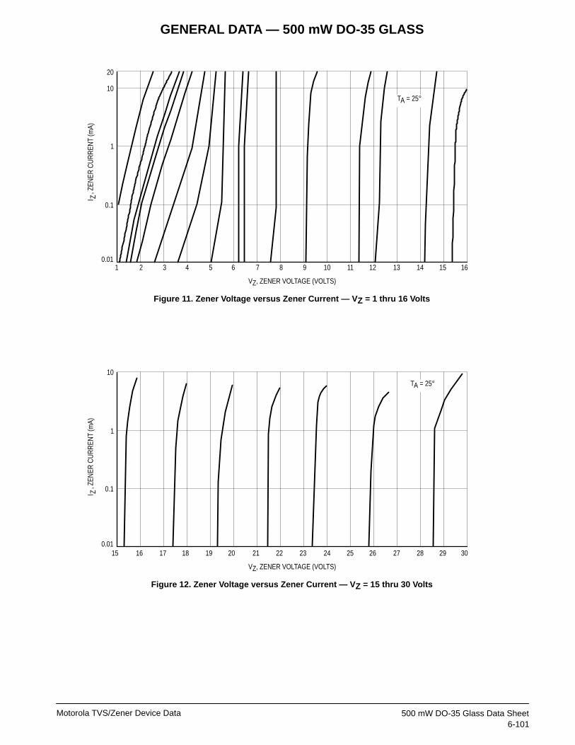
GENERAL DATA — 500 mW DO-35 GLASS
Motorola TVS/Zener Device Data6-98500 mW DO-35 Glass Data Sheet
APPLICATION NOTE — ZENER VOLTAGE
Since the actual voltage available from a given zener diodeis temperature dependent, it is necessary to determine junc-tion temperature under any set of operating conditions in orderto calculate its value. The following procedure is recom-mended:
Lead Temperature, TL, should be determined from:
TL = θLAPD + TA.
θLA is the lead-to-ambient thermal resistance (°C/W) and PD isthe power dissipation. The value for θLA will vary and dependson the device mounting method. θLA is generally 30 to 40°C/Wfor the various clips and tie points in common use and forprinted circuit board wiring.
The temperature of the lead can also be measured using athermocouple placed on the lead as close as possible to the tiepoint. The thermal mass connected to the tie point is normallylarge enough so that it will not significantly respond to heatsurges generated in the diode as a result of pulsed operationonce steady-state conditions are achieved. Using the mea-sured value of TL, the junction temperature may be deter-mined by:
TJ = TL + ∆TJL.
∆TJL is the increase in junction temperature above the leadtemperature and may be found from Figure 2 for dc power:
∆TJL = θJLPD.
For worst-case design, using expected limits of IZ, limits ofPD and the extremes of TJ(∆TJ) may be estimated. Changes involtage, VZ, can then be found from:
∆V = θVZTJ.
θVZ, the zener voltage temperature coefficient, is found fromFigures 4 and 5.
Under high power-pulse operation, the zener voltage willvary with time and may also be affected significantly by thezener resistance. For best regulation, keep current excursionsas low as possible.
Surge limitations are given in Figure 7. They are lower thanwould be expected by considering only junction temperature,as current crowding effects cause temperatures to be ex-tremely high in small spots, resulting in device degradationshould the limits of Figure 7 be exceeded.
L L
500
400
300
200
100
00 0.2 0.4 0.6 0.8 1
2.4–60 V
62–200 V
L, LEAD LENGTH TO HEAT SINK (INCH)JL, J
UN
CTI
ON
-TO
-LEA
D T
HER
MAL
RES
ISTA
NC
E (
C/W
)θ
°
Figure 2. Typical Thermal Resistance
TYPICAL LEAKAGE CURRENTAT 80% OF NOMINALBREAKDOWN VOLTAGE
+25°C
+125°C
100070005000
2000
1000700500
200
1007050
20
1075
2
10.70.5
0.2
0.10.070.05
0.02
0.010.0070.005
0.002
0.0013 4 5 6 7 8 9 10 11 12 13 14 15
VZ, NOMINAL ZENER VOLTAGE (VOLTS)
I, L
EAKA
GE
CU
RR
ENT
(A)µ
R
Figure 3. Typical Leakage Current
GENERAL DATA — 500 mW DO-35 GLASS
Motorola TVS/Zener Device Data6-99
500 mW DO-35 Glass Data Sheet
+12
+10
+8
+6
+4
+2
0
–2
–42 3 4 5 6 7 8 9 10 11 12
VZ, ZENER VOLTAGE (VOLTS)
Figure 4a. Range for Units to 12 Volts
VZ @ IZT(NOTE 2)
RANGE
TEMPERATURE COEFFICIENTS(–55°C to +150°C temperature range; 90% of the units are in the ranges indicated.)
1007050
30
20
10
75
3
2
12 3 4 5 6 7 8 9 10 11 12 10 20 30 50 70 100
VZ, ZENER VOLTAGE (VOLTS)
Figure 4b. Range for Units 12 to 100 Volts
RANGE VZ @ IZ (NOTE 2)
120 130 140 150 160 170 180 190 200
200
180
160
140
120
100
VZ, ZENER VOLTAGE (VOLTS)
Figure 4c. Range for Units 120 to 200 Volts
VZ @ IZT(NOTE 2)
+6
+4
+2
0
–2
–43 4 5 6 7 8
VZ, ZENER VOLTAGE (VOLTS)
Figure 5. Effect of Zener Current
NOTE: BELOW 3 VOLTS AND ABOVE 8 VOLTSNOTE: CHANGES IN ZENER CURRENT DO NOTNOTE: AFFECT TEMPERATURE COEFFICIENTS
1 mA
0.01 mA
VZ @ IZTA = 25°C
1000
C, C
APAC
ITAN
CE
(pF)
500
200
100
50
20
10
5
2
11 2 5 10 20 50 100
VZ, ZENER VOLTAGE (VOLTS)
Figure 6a. Typical Capacitance 2.4–100 Volts
TA = 25°C
0 V BIAS
1 V BIAS
50% OFVZ BIAS
1007050
30
20
1075
3
2
1120 140 160 180 190 200 220
VZ, ZENER VOLTAGE (VOLTS)
Figure 6b. Typical Capacitance 120–200 Volts
TA = 25°C
1 VOLT BIAS
50% OF VZ BIAS
0 BIAS
θVZ
, TEM
PER
ATU
RE
CO
EFFI
CIE
NT
(mV/
°C)
20 mA
C, C
APAC
ITAN
CE
(pF)
θVZ
, TEM
PER
ATU
RE
CO
EFFI
CIE
NT
(mV/
°C)
θVZ
, TEM
PER
ATU
RE
CO
EFFI
CIE
NT
(mV/
°C)
θVZ
, TEM
PER
ATU
RE
CO
EFFI
CIE
NT
(mV/
°C)
GENERAL DATA — 500 mW DO-35 GLASS
Motorola TVS/Zener Device Data6-100500 mW DO-35 Glass Data Sheet
Tolerance DesignationThe type numbers shown have tolerance designations as follows:1N4370A series: ±5% units, C for ±2%, D for ±1%.1N746A series: ±5% units, C for ±2%, D for ±1%.1N957B series: ±5% units, C for ±2%, D for ±1%.
NOTE 2. ZENER VOLTAGE (VZ) MEASUREMENT
Nominal zener voltage is measured with the device junction in thermal equilibrium at the leadtemperature of 30°C ±1°C and 3/8″ lead length.
NOTE 3. ZENER IMPEDANCE (ZZ) DERIVATION
ZZT and ZZK are measured by dividing the ac voltage drop across the device by the ac currentapplied. The specified limits are for IZ(ac) = 0.1 IZ(dc) with the ac frequency = 60 Hz.
NOTE 4. MAXIMUM ZENER CURRENT RATINGS (IZM)
Values shown are based on the JEDEC rating of 400 mW. Where the actual zener voltage(VZ) is known at the operating point, the maximum zener current may be increased and islimited by the derating curve.
The type numbers shown have a standard tolerance of ±5% on the nominal Zener voltage,C for ±2%, D for ±1%.
NOTE 2. MAXIMUM ZENER CURRENT RATINGS (IZM)
Maximum Zener current ratings are based on maximum Zener voltage of the individual unitsand JEDEC 250 mW rating.
NOTE 3. REVERSE LEAKAGE CURRENT (I R)
Reverse leakage currents are guaranteed and measured at VR as shown on the table.
NOTE 4. MAXIMUM VOLTAGE CHANGE ( ∆VZ)
Voltage change is equal to the difference between VZ at 100 µA and VZ at 10 µA.
NOTE 5. ZENER VOLTAGE (VZ) MEASUREMENT
Nominal Zener voltage is measured with the device junction in thermal equilibrium at the leadtemperature at 30°C ±1°C and 3/8″ lead length.
GENERAL DATA — 500 mW DO-35 GLASS
Motorola TVS/Zener Device Data6-106500 mW DO-35 Glass Data Sheet
ELECTRICAL CHARACTERISTICS (TA = 25°C unless otherwise noted. Based on dc measurements at thermal equilibrium; lead length= 3/8″; thermal resistance of heat sink = 30°C/W) VF = 1.1 Max @ IF = 200 mA for all types.
ELECTRICAL CHARACTERISTICS — continued (TA = 25°C unless otherwise noted. Based on dc measurements at thermal equi-librium; lead length = 3/8″; thermal resistance of heat sink = 30°C/W) VF = 1.1 Max @ IF = 200 mA for all types.
The JEDEC type numbers shown indicate a tolerance of ±5%. For tighter tolerance devicesuse suffixes “C” for ±2% and “D” for ±1%.
NOTE 2. TEMPERATURE COEFFICIENT (θVZ)
Test conditions for temperature coefficient are as follows:a. IZT = 7.5 mA, T1 = 25°C,a. T2 = 125°C (1N5221B through 1N5242B).b. IZT = Rated IZT, T1 = 25°C,a. T2 = 125°C (1N5243B through 1N5281B).
Device to be temperature stabilized with current applied prior to reading breakdown voltageat the specified ambient temperature.
NOTE 3. ZENER VOLTAGE (VZ) MEASUREMENT
Nominal zener voltage is measured with the device junction in thermal equilibrium at the leadtemperature of 30°C ±1°C and 3/8″ lead length.
NOTE 4. ZENER IMPEDANCE (ZZ) DERIVATION
ZZT and ZZK are measured by dividing the ac voltage drop across the device by the ac currentapplied. The specified limits are for IZ(ac) = 0.1 IZ(dc) with the ac frequency = 60 Hz.
For more information on special selections contact your nearest Motorola representa-tive.
GENERAL DATA — 500 mW DO-35 GLASS
Motorola TVS/Zener Device Data6-108500 mW DO-35 Glass Data Sheet
*ELECTRICAL CHARACTERISTICS (TL = 30°C unless otherwise noted.) (VF = 1.5 Volts Max @ IF = 100 mAdc for all types.)
MotorolaNominal
Zener Voltage TestMax Zener Impedance (Note 3) Max Reverse Leakage Current Max DC
NOTE 1. TOLERANCE AND VOLTAGE DESIGNATIONTolerance designation — Device tolerances of ±5% are indicated by a “B” suffix, ±2% by a“C” suffix, ±1% by a “D” suffix.
NOTE 2.
This data was calculated using nominal voltages. The maximum current handling capabilityon a worst case basis is limited by the actual zener voltage at the operating point and the pow-er derating curve.
NOTE 3.
ZZT and ZZK are measured by dividing the ac voltage drop across the device by the ac currentapplied. The specified limits are for IZ(ac) = 0.1 IZ(dc) with the ac frequency = 1.0 kHz.
NOTE 4.
Nominal Zener Voltage (VZ) is measured with the device junction in thermal equilibrium at thelead temperature of 30°C ±1°C and 3/8″ lead length.
@
GENERAL DATA — 500 mW DO-35 GLASS
Motorola TVS/Zener Device Data6-109
500 mW DO-35 Glass Data Sheet
ELECTRICAL CHARACTERISTICS (TL = 30°C unless otherwise noted.) (VF = 1.3 Volts Max, IF = 100 mAdc for all types.)
Tolerance designation — The type numbers listed have zener voltage min/max limits asshown. Device tolerance of ±2% are indicated by a “B” instead of a “C”. Zener voltage is mea-sured with the device junction in thermal equilibrium at the lead temperature of 30°C ±1°Cand 3/8″ lead length.
NOTE 2.
This data was calculated using nominal voltages. The maximum current handling capability
on a worst case basis is limited by the actual zener voltage at the operating point and the pow-er derating curve.
NOTE 3.
ZZT and ZZK are measured by dividing the ac voltage drop across the device by the ac currentapplied. The specified limtis are for IZ(ac) = 0.1 IZ(dc) with the ac frequency = 1.0 kHz.
GENERAL DATA — 500 mW DO-35 GLASS
Motorola TVS/Zener Device Data6-110500 mW DO-35 Glass Data Sheet
*ELECTRICAL CHARACTERISTICS (TL = 30°C unless otherwise noted.) (VF = 1.5 Volts Max @ IF = 100 mAdc for all types.)
NOTE 1. Zener voltage is measured under pulse conditions such that TJ is no more than 2°Cabove TA.
NOTE 2. TOLERANCE AND VOLTAGE DESIGNATION
Tolerance designation —– The type numbers listed have zener voltage min/max limits as
shown. Device tolerances of ±2% are indicated by a “B” instead of a “C,” and ±1% by “A.”
NOTE 3. ZZT is measured by dividing the ac voltage drop across the device by the ac currentapplied. The specified limits are for IZ(ac) = 0.1 IZ(dc) with the ac frequency = 1.0 kHz.
GENERAL DATA — 500 mW DO-35 GLASS
Motorola TVS/Zener Device Data6-111
500 mW DO-35 Glass Data Sheet
ELECTRICAL CHARACTERISTICS (at TA = 25°C)Motorola ZPD and BZX83C series. Forward Voltage VF = 1 Volt Max at IF = 50 mA.
Zener Voltage (Note 1)at IZT = 5.0 mA
Impedance ( Ω)Max (Note 2) Typ. Temp.
C ff
VR Min
at IZ = 1 mA
yp pCoeff.at IZT
V
Device Type Nominal Min Max at IZT BZX83 ZPDat IZT
Motorola TVS/Zener Device Data6-112500 mW DO-35 Glass Data Sheet
Designed for 250 mW applications requiring low leakage,low impedance. Same as 1N4099 through 1N4104 and1N4614 through 1N4627 except low noise test omitted.
• Voltage Range from 1.8 to 10 Volts• Zener Impedance and Zener Voltage Specified for Low-
Level Operation at IZT = 250 µA
ELECTRICAL CHARACTERISTICS (TA = 25°C unless otherwise specified. IZT = 250 µA and VF = 1 V Max @ IF = 200 mA for allELECTRICAL CHARACTERISTICS types)
NOTE 1. TOLERANCE AND VOLTAGE DESIGNATIONThe type numbers shown have a standard tolerance of ±5% on the nominal zener voltage.
NOTE 2. ZENER VOLTAGE (VZ) MEASUREMENT
Nominal Zener Voltage is measured with the device junction in the thermal equilibrium withambient temperature of 25°C.
NOTE 3. ZENER IMPEDANCE (ZZT) DERIVATION
The zener impedance is derived from the 60 cycle ac voltage, which results when an ac cur-rent having an rms value equal to 10% of the dc zener current (IZT) is superimposed on IZT.
NOTE 4. MAXIMUM ZENER CURRENT RATINGS (IZM)
Maximum zener current ratings are based on maximum zener voltage of the individual units.
NOTE 5. REVERSE LEAKAGE CURRENT I RReverse leakage currents are guaranteed and are measured at VR as shown on the table.
NOTE 6. SPECIAL SELECTORS AVAILABLE INCLUDE:
A) Tighter voltage tolerances. Contact your nearest Motorola representative for more infor-mation.
GENERAL DATA — 500 mW DO-35 GLASS
Motorola TVS/Zener Device Data6-113
500 mW DO-35 Glass Data Sheet
Low Voltage Avalanche PassivatedSilicon Oxide Zener Regulator DiodesSame as 1N5520B through 1N5530B except low noise testspec omitted.• Low Maximum Regulation Factor• Low Zener Impedance• Low Leakage Current
ELECTRICAL CHARACTERISTICS (TA = 25°C unless otherwise specified. Based on dc measurements at thermal equilibrium;ELECTRICAL CHARACTERISTICS VF = 1.1 Max @ IF = 200 mA for all types.)
M l
NominalZener
TMax Zener
Max Reverse Leakage Current MaximumDC Zener Regulation Low
The “B” suffix type numbers listed are ±5% tolerance of nominal VZ.
NOTE 2. ZENER VOLTAGE (VZ) MEASUREMENT
Nominal zener voltage is measured with the device junction in thermal equilibrium with ambi-ent temperature of 25°C.
NOTE 3. ZENER IMPEDANCE (ZZ) DERIVATION
The zener impedance is derived from the 60 Hz ac voltage, which results when an ac currenthaving an rms value equal to 10% of the dc zener current (IZT) is superimposed on IZT.
NOTE 4. REVERSE LEAKAGE CURRENT I RReverse leakage currents are guaranteed and are measured at VR as shown on the table.
NOTE 5. MAXIMUM REGULATOR CURRENT (I ZM)
The maximum current shown is based on the maximum voltage of a ±5% type unit, therefore,it applies only to the “B” suffix device. The actual IZM for any device may not exceed the valueof 400 milliwatts divided by the actual VZ of the device.
NOTE 6. MAXIMUM REGULATION FACTOR ( ∆VZ)
∆VZ is the maximum difference between VZ at IZT and VZ at IZL measured with the devicejunction in thermal equilibrium.
NOTE 7. SPECIAL SELECTORS AVAILABLE INCLUDE:
A) Tighter voltage tolerances. Contact your nearest Motorola representative for more infor-mation.
GENERAL DATA — 500 mW DO-35 GLASS
Motorola TVS/Zener Device Data6-114500 mW DO-35 Glass Data Sheet
500 mW DO-35 Glass
MULTIPLE PACKAGE QUANTITY (MPQ)REQUIREMENTS
Zener Voltage Regulator Diodes — Axial Leaded
CASE 299-02DO-204AH
GLASS
(Refer to Section 10 for Surface Mount, Thermal Data and Footprint Information.)
Refer to Section 10 for more information on Packaging Specifications.
MIN MINMAX MAXMILLIMETERS INCHES
DIM3.051.520.46—
25.40
5.082.290.561.2738.10
0.1200.0600.018—
1.000
0.2000.0900.0220.0501.500
ABDFK
All JEDEC dimensions and notes apply.
NOTES:1. PACKAGE CONTOUR OPTIONAL WITHIN A AND B
HEAT SLUGS, IF ANY, SHALL BE INCLUDEDWITHIN THIS CYLINDER, BUT NOT SUBJECT TOTHE MINIMUM LIMIT OF B.
2. LEAD DIAMETER NOT CONTROLLED IN ZONE FTO ALLOW FOR FLASH, LEAD FINISH BUILDUPAND MINOR IRREGULARITIES OTHER THANHEAT SLUGS.
3. POLARITY DENOTED BY CATHODE BAND.4. DIMENSIONING AND TOLERANCING PER ANSI
Y14.5M, 1982.
B
A
KD
F
F
K
Package Option
Tape and Reel 5K
Type No. Suffix
RL, RL2(1)
MPQ (Units)
Tape and Ammo TA, TA2(1) 5K
NOTES: 1. The “2” suffix refers to 26 mm tape spacing.NOTES: 2. Radial Tape and Reel may be available. Please contact your MotorolaNOTES: 2. representative.
GENERAL DATA — 500 mW DO-35 GLASS
Motorola TVS/Zener Device Data6-115
500 mW DO-35 Glass Data Sheet
1–1.3 Watt DO-41 GlassZener Voltage Regulator DiodesGENERAL DATA APPLICABLE TO ALL SERIES INTHIS GROUP
One Watt Hermetically Sealed GlassSilicon Zener Diodes
Specification Features:• Complete Voltage Range — 3.3 to 100 Volts• DO-41 Package• Double Slug Type Construction• Metallurgically Bonded Construction• Oxide Passivated Die
Mechanical Characteristics:
CASE: Double slug type, hermetically sealed glassMAXIMUM LEAD TEMPERATURE FOR SOLDERING PURPOSES: 230°C, 1/16″ from
case for 10 secondsFINISH: All external surfaces are corrosion resistant with readily solderable leadsPOLARITY: Cathode indicated by color band. When operated in zener mode, cathode
will be positive with respect to anodeMOUNTING POSITION: AnyWAFER FAB LOCATION: Phoenix, ArizonaASSEMBLY/TEST LOCATION: Seoul, Korea
MAXIMUM RATINGS
Rating Symbol Value Unit
DC Power Dissipation @ TA = 50°CDerate above 50°C
PD 16.67
WattmW/°C
Operating and Storage Junction Temperature Range TJ, Tstg – 65 to +200 °C
Figure 1. Power Temperature Derating Curve
TL, LEAD TEMPERATURE (°C)
P ,
MAX
IMU
M D
ISSI
PATI
ON
(WAT
TS)
D
0 20 40 60 20080 100 120 140 160 180
0.25
0.5
0.75
1
1.25L = LEAD LENGTH TO HEAT SINK
L = 3/8″L = 1/8″L = 1″
GENERALDATA
CASE 59-03DO-41GLASS
1–1.3 WATTDO-41 GLASS
1 WATTZENER REGULATOR
DIODES3.3–100 VOLTS
GENERAL DATA — 500 mW DO-35 GLASS
Motorola TVS/Zener Device Data6-116500 mW DO-35 Glass Data Sheet
Figure 2. Temperature Coefficients(–55°C to +150°C temperature range; 90% of the units are in the ranges indicated.)
a. Range for Units to 12 Volts b. Range for Units to 12 to 100 Volts
+12
+10
+8
+6
+4
+2
0
–2
–42 3 4 5 6 7 8 9 10 11 12
VZ, ZENER VOLTAGE (VOLTS)
θVZ
, TEM
PER
ATU
RE
CO
EFFI
CIE
NT
(mV/
°C) 100
7050
30
20
1075
3
2
110 20 30 50 70 100
VZ, ZENER VOLTAGE (VOLTS)
θVZ
, TEM
PER
ATU
RE
CO
EFFI
CIE
NT
(mV/
°C)
VZ @ IZTRANGE
RANGE VZ @ IZT
Figure 3. Typical Thermal Resistanceversus Lead Length
Figure 4. Effect of Zener Current
175
150
125
100
75
50
25
00 0.1 0.2 0.3 0.4 0.5 0.6 0.7 0.8 0.9 1
L, LEAD LENGTH TO HEAT SINK (INCHES)θ JL
, JU
NC
TIO
N-T
O-L
EAD
TH
ERM
AL R
ESIS
TAN
CE
(mV/
°C/W
)
θVZ
, TEM
PER
ATU
RE
CO
EFFI
CIE
NT
(mV/
°C) +6
+4
+2
0
–2
–43 4 5 6 7 8
VZ, ZENER VOLTAGE (VOLTS)
VZ @ IZTA = 25°C
20 mA
0.01 mA1 mA
NOTE: BELOW 3 VOLTS AND ABOVE 8 VOLTSNOTE: CHANGES IN ZENER CURRENT DO NOTNOTE: EFFECT TEMPERATURE COEFFICIENTS
Figure 6. Effect of Zener Currenton Zener Impedance
Figure 7. Effect of Zener Voltageon Zener Impedance
Figure 9. Typical Capacitance versus V Z
Figure 8. Typical Leakage Current
1000500
200
100
50
20
10
5
2
10.1 0.2 0.5 1 2 5 10 20 50 100
IZ, ZENER CURRENT (mA)
ZZ
, DYN
AMIC
IMPE
DAN
CE
(OH
MS)
1000700500
200
1007050
20
1075
2
11 2 100
VZ, ZENER CURRENT (mA)3 5 7 10 20 30 50 70
ZZ
, DYN
AMIC
IMPE
DAN
CE
(OH
MS)
1000070005000
2000
1000700500
200
1007050
20
1075
2
10.70.5
0.2
0.10.070.05
0.02
0.010.0070.005
0.002
0.001
I R, L
EAKA
GE
CU
RR
ENT
(µA)
3 4 5 6 7 8 9 10 11 12 13 14 15
VZ, NOMINAL ZENER VOLTAGE (VOLTS)
+25°C
+125°C
TYPICAL LEAKAGE CURRENTAT 80% OF NOMINALBREAKDOWN VOLTAGE
TJ = 25°CiZ(rms) = 0.1 IZ(dc)f = 60 Hz
6.2 V
27 V
VZ = 2.7 V
47 V
TJ = 25°CiZ(rms) = 0.1 IZ(dc)f = 60 Hz
20 mA
5 mA
IZ = 1 mA
0 V BIAS
1 V BIAS
400300
200
100
50
20
108
41 2 5 10 20 50 100
VZ, NOMINAL VZ (VOLTS)
C, C
APAC
ITAN
CE
(pF)
50% OF BREAKDOWN BIAS
MINIMUM
GENERAL DATA — 500 mW DO-35 GLASS
Motorola TVS/Zener Device Data6-118500 mW DO-35 Glass Data Sheet
APPLICATION NOTE
Since the actual voltage available from a given zener diodeis temperature dependent, it is necessary to determine junc-tion temperature under any set of operating conditions in orderto calculate its value. The following procedure is recom-mended:
Lead Temperature, TL, should be determined from:
TL = θLAPD + TA.
θLA is the lead-to-ambient thermal resistance (°C/W) and PD isthe power dissipation. The value for θLA will vary and dependson the device mounting method. θLA is generally 30 to 40°C/Wfor the various clips and tie points in common use and forprinted circuit board wiring.
The temperature of the lead can also be measured using athermocouple placed on the lead as close as possible to the tiepoint. The thermal mass connected to the tie point is normallylarge enough so that it will not significantly respond to heatsurges generated in the diode as a result of pulsed operationonce steady-state conditions are achieved. Using the mea-sured value of TL, the junction temperature may be deter-mined by:
TJ = TL + ∆TJL.∆TJL is the increase in junction temperature above the lead
temperature and may be found as follows:
∆TJL = θJLPD.
θJL may be determined from Figure 3 for dc power condi-tions. For worst-case design, using expected limits of IZ, limitsof PD and the extremes of TJ(∆TJ) may be estimated. Changesin voltage, VZ, can then be found from:
∆V = θVZ ∆TJ.
θVZ, the zener voltage temperature coefficient, is found fromFigure 2.
Under high power-pulse operation, the zener voltage willvary with time and may also be affected significantly by thezener resistance. For best regulation, keep current excursionsas low as possible.
Surge limitations are given in Figure 5. They are lower thanwould be expected by considering only junction temperature,as current crowding effects cause temperatures to be ex-tremely high in small spots, resulting in device degradationshould the limits of Figure 5 be exceeded.
GENERAL DATA — 500 mW DO-35 GLASS
Motorola TVS/Zener Device Data6-119
500 mW DO-35 Glass Data Sheet
*ELECTRICAL CHARACTERISTICS (TA = 25°C unless otherwise noted) VF = 1.2 V Max, IF = 200 mA for all types.
JEDEC
NominalZener Voltage Test
Maximum Zener Impedance (Note 4) Leakage CurrentSurge Current @
The JEDEC type numbers listed have a standard tolerance on the nominal zener voltage of±5%. C for ±2%, D for ±1%.
NOTE 2. SPECIALS AVAILABLE INCLUDE:
Nominal zener voltages between the voltages shown and tighter voltage tolerances.
For detailed information on price, availability, and delivery, contact your nearest Motorola rep-resentative.
NOTE 3. ZENER VOLTAGE (VZ) MEASUREMENT
Motorola guarantees the zener voltage when measured at 90 seconds while maintaining thelead temperature (TL) at 30°C ± 1°C, 3/8″ from the diode body.
NOTE 4. ZENER IMPEDANCE (ZZ) DERIVATION
The zener impedance is derived from the 60 cycle ac voltage, which results when an ac cur-rent having an rms value equal to 10% of the dc zener current (IZT or IZK) is superimposedon IZT or IZK.
NOTE 5. SURGE CURRENT (ir) NON-REPETITIVE
The rating listed in the electrical characteristics table is maximum peak, non-repetitive, re-verse surge current of 1/2 square wave or equivalent sine wave pulse of 1/120 second dura-tion superimposed on the test current, IZT, per JEDEC registration; however, actual devicecapability is as described in Figure 5 of the General Data — DO-41 Glass.
GENERAL DATA — 500 mW DO-35 GLASS
Motorola TVS/Zener Device Data6-120500 mW DO-35 Glass Data Sheet
ELECTRICAL CHARACTERISTICS (TA = 25°C unless otherwise noted.) (VF = 1.2 V Max, IF = 200 mA for all types.)
The type numbers listed have zener voltage min/max limits as shown. Device tolerance of±2% are indicated by a “B” instead of “C.”
NOTE 2. SPECIALS AVAILABLE INCLUDE:
Nominal zener voltages between the voltages shown and tighter voltage tolerances.
For detailed information on price, availability, and delivery, contact your nearest Motorola rep-resentative.
NOTE 3. ZENER VOLTAGE (VZ) MEASUREMENTVZ is measured after the test current has been applied to 40 ± 10 msec., while maintainingthe lead temperature (TL) at 30°C ± 1°C, 3/8″ from the diode body.
NOTE 4. ZENER IMPEDANCE (ZZ) DERIVATION
The zener impedance is derived from the 1 kHz cycle ac voltage, which results when an accurrent having an rms value equal to 10% of the dc zener current (IZT) or (IZK) is superim-posed on IZT or IZK.
NOTE 5. SURGE CURRENT (ir) NON-REPETITIVE
The rating listed in the electrical characteristics table is maximum peak, non-repetitive, re-verse surge current of 1/2 square wave or equivalent sine wave pulse of 1/120 second dura-tion superimposed on the test current IZT. However, actual device capability is as describedin Figure 5 of General Data DO-41 glass.
GENERAL DATA — 500 mW DO-35 GLASS
Motorola TVS/Zener Device Data6-121
500 mW DO-35 Glass Data Sheet
ELECTRICAL CHARACTERISTICS (TA = 25°C unless otherwise noted) VF = 1.2 V Max, IF = 200 mA for all types.
The type numbers listed have zener voltage min/max limits as shown. Device tolerance of±2% are indicated by a “C” and ±1% by a “D” suffix.
NOTE 2. SPECIALS AVAILABLE INCLUDE:
Nominal zener voltages between the voltages shown and tighter voltage tolerances.
For detailed information on price, availability, and delivery, contact your nearest Motorola rep-resentative.
NOTE 3. ZENER VOLTAGE (VZ) MEASUREMENTVZ is measured after the test current has been applied to 40 ± 10 msec., while maintainingthe lead temperature (TL) at 30°C ± 1°C, 3/8″ from the diode body.
NOTE 4. ZENER IMPEDANCE (ZZ) DERIVATION
The zener impedance is derived from the 1 kHz cycle ac voltage, which results when an accurrent having an rms value equal to 10% of the dc zener current (IZT) of (IZK) is superim-posed on IZT or IZK.
NOTE 5. SURGE CURRENT (ir) NON-REPETITIVE
The rating listed in the electrical characteristics table is maximum peak, non-repetitive, re-verse surge current of 1/2 square wave or equivalent sine wave pulse of 1/120 second dura-tion superimposed on the test current IZT, however, actual device capability is as describedin Figure 5 of General Data DO-41 glass.
GENERAL DATA — 500 mW DO-35 GLASS
Motorola TVS/Zener Device Data6-122500 mW DO-35 Glass Data Sheet
1–1.3 Watt DO-41 Glass
MULTIPLE PACKAGE QUANTITY (MPQ)REQUIREMENTS
Zener Voltage Regulator Diodes — Axial Leaded
CASE 59-03DO-41GLASS
(Refer to Section 10 for Surface Mount, Thermal Data and Footprint Information.)
(Refer to Section 10 for more information on Packaging Specifications.)
Package Option
Tape and Reel 6K
Type No. Suffix
RL, RL2
MPQ (Units)
Tape and Ammo TA, TA2 4K
NOTES:1. ALL RULES AND NOTES ASSOCIATED WITH
JEDEC DO-41 OUTLINE SHALL APPLY.2. POLARITY DENOTED BY CATHODE BAND.3. LEAD DIAMETER NOT CONTROLLED WITHIN F
DIMENSION.
K
K
F
A
F
D
MIN MINMAX MAXMILLIMETERS INCHES
DIM4.072.040.71—
27.94
5.202.710.861.27—
0.1600.0800.028
— 1.100
0.2050.1070.0340.050
—
ABDFK
B
NOTE: 1. The “2” suffix refers to 26 mm tape spacing.
GENERAL DATA — 500 mW DO-35 GLASS
Motorola TVS/Zener Device Data6-123
500 mW DO-35 Glass Data Sheet
1 to 3 Watt DO-41 Surmetic 30Zener Voltage Regulator DiodesGENERAL DATA APPLICABLE TO ALL SERIES INTHIS GROUP
1 to 3 Watt Surmetic 30Silicon Zener Diodes. . . a complete series of 1 to 3 Watt Zener Diodes with limits and operating characteristicsthat reflect the superior capabilities of silicon-oxide-passivated junctions. All this in anaxial-lead, transfer-molded plastic package offering protection in all common environmen-tal conditions.
Specification Features:• Surge Rating of 98 Watts @ 1 ms• Maximum Limits Guaranteed On Up To Six Electrical Parameters• Package No Larger Than the Conventional 1 Watt Package
Mechanical Characteristics:
CASE: Void-free, transfer-molded, thermosetting plasticFINISH: All external surfaces are corrosion resistant and leads are readily solderablePOLARITY: Cathode indicated by color band. When operated in zener mode, cathode
will be positive with respect to anodeMOUNTING POSITION: AnyWEIGHT: 0.4 gram (approx)WAFER FAB LOCATION: Phoenix, ArizonaASSEMBLY/TEST LOCATION: Seoul, Korea
MAXIMUM RATINGS
Rating Symbol Value Unit
DC Power Dissipation @ TL = 75°CLead Length = 3/8″Derate above 75°C
PD 3
24
Watts
mW/°C
DC Power Dissipation @ TA = 50°CDerate above 50°C
PD 16.67
WattmW/°C
Operating and Storage Junction Temperature Range TJ, Tstg – 65 to +200 °C
GENERALDATA
CASE 59-03DO-41
PLASTIC
1–3 WATTDO-41
SURMETIC 30
1 TO 3 WATTZENER REGULATOR
DIODES3.3–400 VOLTS
Figure 1. Power Temperature Derating Curve
TL, LEAD TEMPERATURE (°C)
P ,
MAX
IMU
M D
ISSI
PATI
ON
(WAT
TS)
D
0 20 40 60 20080 100 120 140 160 1800
1
2
3
4
5
L = 1/8″
L = 3/8″
L = 1″
L = LEAD LENGTH TO HEAT SINK
GENERAL DATA — 500 mW DO-35 GLASS
Motorola TVS/Zener Device Data6-124500 mW DO-35 Glass Data Sheet
Since the actual voltage available from a given zener diodeis temperature dependent, it is necessary to determine junc-tion temperature under any set of operating conditions in orderto calculate its value. The following procedure is recom-mended:
Lead Temperature, TL, should be determined from:
TL = θLA PD + TAθLA is the lead-to-ambient thermal resistance (°C/W) andPD is the power dissipation. The value for θLA will vary anddepends on the device mounting method. θLA is generally30–40°C/W for the various clips and tie points in commonuse and for printed circuit board wiring.
The temperature of the lead can also be measured using athermocouple placed on the lead as close as possible to the tiepoint. The thermal mass connected to the tie point is normallylarge enough so that it will not significantly respond to heatsurges generated in the diode as a result of pulsed operationonce steady-state conditions are achieved. Using the mea-sured value of TL, the junction temperature may be deter-mined by:
TJ = TL + ∆TJL
∆TJL is the increase in junction temperature above the leadtemperature and may be found from Figure 2 for a train ofpower pulses (L = 3/8 inch) or from Figure 10 for dc power.
∆TJL = θJL PD
For worst-case design, using expected limits of IZ, limits ofPD and the extremes of TJ (∆TJ) may be estimated. Changesin voltage, VZ, can then be found from:
∆V = θVZ ∆TJ
θVZ, the zener voltage temperature coefficient, is found fromFigures 5 and 6.Under high power-pulse operation, the zener voltage will
vary with time and may also be affected significantly by thezener resistance. For best regulation, keep current excursionsas low as possible.
Data of Figure 2 should not be used to compute surge capa-bility. Surge limitations are given in Figure 3. They are lowerthan would be expected by considering only junction tempera-ture, as current crowding effects cause temperatures to be ex-tremely high in small spots resulting in device degradationshould the limits of Figure 3 be exceeded.
GENERAL DATA — 500 mW DO-35 GLASS
Motorola TVS/Zener Device Data6-125
500 mW DO-35 Glass Data Sheet
Figure 5. Units To 12 Volts Figure 6. Units 10 To 400 Volts
Figure 7. V Z = 3.3 thru 10 Volts Figure 8. V Z = 12 thru 82 Volts
Figure 9. V Z = 100 thru 400 Volts Figure 10. Typical Thermal Resistance
ZENER VOLTAGE versus ZENER CURRENT(Figures 7, 8 and 9)
TEMPERATURE COEFFICIENT RANGES(90% of the Units are in the Ranges Indicated)
NOTE 1. TOLERANCE AND VOLTAGE DESIGNATIONTolerance designation — Device tolerances of ±5% are indicated by a “B” suffix.
NOTE 2. SPECIAL SELECTIONS AVAILABLE INCLUDE:Nominal zener voltages between those shown and ±1% and ±2% tight voltage tolerances.Consult factory.
NOTE 3. ZENER VOLTAGE (VZ) MEASUREMENT
Motorola guarantees the zener voltage when meausred at 90 seconds while maintaining thelead temperature (TL) at 30°C ±1°C, 3/8″ from the diode body.
NOTE 4. ZENER IMPEDANCE (ZZ) DERIVATION
The zener impedance is derived from the 60 cycle ac voltage, which results when an ac cur-rent having an rms value equal to 10% of the dc zener current (IZT or IZK) is superimposedon IZT or IZK.
GENERAL DATA — 500 mW DO-35 GLASS
Motorola TVS/Zener Device Data6-128500 mW DO-35 Glass Data Sheet
ELECTRICAL CHARACTERISTICS (TA = 25°C unless otherwise noted) VF = 1.5 V Max, IF = 200 mA for all types)
Suffix 5 indicates 5% tolerance. Any other tolerance will be considered as a special device.
NOTE 2. ZENER VOLTAGE (VZ) MEASUREMENTMotorola guarantees the zener voltage when measured at 40 ms ±10 ms 3/8″ from the diodebody, and an ambient temperature of 25°C (+8°C, –2°C)
NOTE 3. ZENER IMPEDANCE (ZZ) DERIVATION
The zener impedance is derived from the 60 cycle ac voltage, which results when an ac cur-rent having an rms value equal to 10% of the dc zener current (IZT or IZK) is superimposedon IZT or IZK.
NOTE 4. SURGE CURRENT (ir) NON-REPETITIVE
The rating listed in the electrical characteristics table is maximum peak, non-repetitive, re-verse surge current of 1/2 square wave or equivalent sine wave pulse of 1/120 second dura-tion superimposed on the test current, IZT, per JEDEC standards, however, actual device ca-pability is as described in Figure 3 of General Data sheet for Surmetic 30s.
NOTE 5. SPECIAL SELECTIONS AVAILABLE INCLUDE:Nominal zener voltages between those shown. Tight voltage tolerances such as ±1% and±2%. Consult factory.
GENERAL DATA — 500 mW DO-35 GLASS
Motorola TVS/Zener Device Data6-130500 mW DO-35 Glass Data Sheet
ELECTRICAL CHARACTERISTICS (TA = 25°C unless otherwise noted.) VF = 1.5 V Max, IF = 200 mA for all types.
NOTE 1. TOLERANCE AND TYPE NUMBER DESIGNATIONThe type numbers listed have zener voltage min/max limits as shown.
NOTE 2. ZENER VOLTAGE (VZ) MEASUREMENTThe zener voltage is measured after the test current (IZT) has been applied for 40±10 millisec-onds, while maintaining a lead temperautre (TL) of 30°C at a point of 10 mm from the diodebody.
NOTE 3. (ir) NON-REPETITIVE SURGE CURRENT
Maximum peak, non-repetitive reverse surge current of half square wave or equivalent sinewave pulse of 50 ms duration, superimposed on the test current (IZT).
NOTE 4. SPECIAL SELECTIONS AVAILABLE INCLUDE:
Nominal zener voltages between those shown. Tight voltage tolerances such as ±1% and±2%. Consult factory.
GENERAL DATA — 500 mW DO-35 GLASS
Motorola TVS/Zener Device Data6-131
500 mW DO-35 Glass Data Sheet
ELECTRICAL CHARACTERISTICS (TA = 25°C unless otherwise noted) VF = 1.5 V Max, lF = 200 mA for all types
The type numbers listed have a standard tolerance on the nominal zener voltage of ±5%. Thetolerance on the 1M type numbers is indicated by the digits following ZS in the part number.“5” indicates a ±5% VZ tolerance.
NOTE 1. TOLERANCE AND TYPE NUMBER DESIGNATION
NOTE 4. SURGE CURRENT (ir) NON-REPETITIVE
NOTE 2. ZENER VOLTAGE (VZ) MEASUREMENTMotorola guarantees the zener voltage when measured at 90 seconds while maintaining thelead temperature (TL) at 30°C ±1°C, 3/8″ from the diode body.
NOTE 3. ZENER IMPEDANCE (ZZ) DERIVATIONThe zener impedance is derived from the 60 cycle ac voltage, which results when an ac
The rating listed in the electrical characteristics table is maximum peak, non-repetitive,reverse surge current of 1/2 square wave or equivalent sine wave pulse of 1/120 secondduration superimposed on the test current, IZT, however, actual device capability is asdescribed in Figure 3 of General Data — Surmetic 30.
NOTE 5. SPECIAL SELECTIONS AVAILABLE INCLUDE:Nominal zener voltages between those shown. Tight voltage tolerances such as ±1% and±2%. Consult factory.
current having an rms value equal to 10% of the dc zener current (IZT or IZK) is superimposedon IZT or IZK.
GENERAL DATA — 500 mW DO-35 GLASS
Motorola TVS/Zener Device Data6-132500 mW DO-35 Glass Data Sheet
1–3 Watt DO-41 Surmetic 30
MULTIPLE PACKAGE QUANTITY (MPQ)REQUIREMENTS
Zener Voltage Regulator Diodes — Axial Leaded
CASE 59-03DO-41
PLASTIC
(Refer to Section 10 for Surface Mount, Thermal Data and Footprint Information.)
(Refer to Section 10 for more information on Packaging Specifications.)
Package Option
Tape and Reel 6K
Type No. Suffix
RL
MPQ (Units)
Tape and Ammo TA 4K
NOTES:1. ALL RULES AND NOTES ASSOCIATED WITH
JEDEC DO-41 OUTLINE SHALL APPLY.2. POLARITY DENOTED BY CATHODE BAND.3. LEAD DIAMETER NOT CONTROLLED WITHIN F
DIMENSION.
K
K
F
A
F
D
MIN MINMAX MAXMILLIMETERS INCHES
DIM4.072.040.71—
27.94
5.202.710.861.27—
0.1600.0800.028
— 1.100
0.2050.1070.0340.050
—
ABDFK
B
MOTOROLASEMICONDUCTORTECHNICAL DATA
Motorola TVS/Zener Device Data6-1335 Watt Surmetic 40 Data Sheet
5 Watt Surmetic 40Silicon Zener Diodes
This is a complete series of 5 Watt Zener Diodes with tight limits and better operatingcharacteristics that reflect the superior capabilities of silicon-oxide-passivated junctions.All this is in an axial-lead, transfer-molded plastic package that offers protection in all com-mon environmental conditions.
Specification Features:• Up to 180 Watt Surge Rating @ 8.3 ms• Maximum Limits Guaranteed on Seven Electrical Parameters
Mechanical Characteristics:
CASE: Void-free, transfer-molded, thermosetting plasticFINISH: All external surfaces are corrosion resistant and leads are readily solderablePOLARITY: Cathode indicated by color band. When operated in zener mode, cathode
will be positive with respect to anodeMOUNTING POSITION: AnyWEIGHT: 0.7 gram (approx)WAFER FAB LOCATION: Phoenix, ArizonaASSEMBLY/TEST LOCATION: Seoul, Korea
MAXIMUM RATINGS
Rating Symbol Value Unit
DC Power Dissipation @ TL = 75°CLead Length = 3/8″Derate above 75°C
PD 5
40
Watts
mW/°C
Operating and Storage Junction Temperature Range TJ, Tstg – 65 to +200 °C
Figure 1. Power Temperature Derating Curve
TL, LEAD TEMPERATURE (°C)
PD
, MAX
IMU
M P
OW
ER D
ISSI
PATI
ON
(WAT
TS) 8
6
4
2
00 20 40 60 80 100 120 140 160 180 200
L = LEAD LENGTHL = TO HEAT SINKL = (SEE FIGURE 5)L = 1/8″
L = 3/8″
L = 1″
1N5333Bthrough1N5388B
CASE 17PLASTIC
5 WATTZENER REGULATOR
DIODES3.3–200 VOLTS
1N5333B through 1N5388B
Motorola TVS/Zener Device Data6-1345 Watt Surmetic 40 Data Sheet
Devices listed in bold, italic are Motorola preferred devices.
ELECTRICAL CHARACTERISTICS (TA = 25°C unless otherwise noted, VF = 1.2 Max @ IF = 1 A for all types)
NOTE 1. TOLERANCE AND TYPE NUMBER DESIGNATIONThe JEDEC type numbers shown indicate a tolerance of ±5%.
NOTE 2. ZENER VOLTAGE (VZ) AND IMPEDANCE (ZZT & ZZK)
Test conditions for zener voltage and impedance are as follows: IZ is applied 40 ± 10 ms priorto reading. Mounting contacts are located 3/8″ to 1/2″ from the inside edge of mounting clipsto the body of the diode. (TA = 25°C +8, –2°C).
NOTE 3. SURGE CURRENT (ir)
Surge current is specified as the maximum allowable peak, non-recurrent square-wave cur-rent with a pulse width, PW, of 8.3 ms. The data given in Figure 6 may be used to find themaximum surge current for a square wave of any pulse width between 1ms and 1000 ms byplotting the applicable points on logarithmic paper. Examples of this, using the 3.3 V and200 V zeners, are shown in Figure 7. Mounting contact located as specified in Note 3. (TA =25°C +8, –2°C.)
NOTE 4. VOLTAGE REGULATION ( ∆VZ)
Test conditions for voltage regulation are as follows: VZ measurements are made at 10% andthen at 50% of the IZ max value listed in the electrical characteristics table. The test currenttime duration for each VZ measurement is 40 ± 10 ms. (TA = 25°C +8, –2°C). Mounting contactlocated as specified in Note 2.
NOTE 5. MAXIMUM REGULATOR CURRENT (I ZM)
The maximum current shown is based on the maximum voltage of a 5% type unit, therefore,it applies only to the B-suffix device. The actual IZM for any device may not exceed the valueof 5 watts divided by the actual VZ of the device. TL = 75°C at 3/8″ maximum from the devicebody.
NOTE 6. SPECIALS AVAILABLE INCLUDE:
Nominal zener voltages between the voltages shown and tighter voltage tolerance such as±1% and ±2%. Consult factory.
TEMPERATURE COEFFICIENTS
Figure 2. Temperature Coefficient-Rangefor Units 3 to 10 Volts
Figure 3. Temperature Coefficient-Rangefor Units 10 to 220 Volts
VZ, ZENER VOLTAGE @ IZT (VOLTS)
10
8
6
4
2
0
–2
3 4 5 6 7 8 9 10
RANGE
300200
100
50
3020
10
50 20 40 60 80 100 120 140 160 180 200 220
VZ, ZENER VOLTAGE @ IZT (VOLTS)
θVZ
, TEM
PER
ATU
RE
CO
EFFI
CIE
NT
(mV/
°C) @
IZT
θVZ
, TEM
PER
ATU
RE
CO
EFFI
CIE
NT
(mV/
°C) @
IZT RANGE
1N5333B through 1N5388B
Motorola TVS/Zener Device Data6-1365 Watt Surmetic 40 Data Sheet
Devices listed in bold, italic are Motorola preferred devices.
Figure 4. Typical Thermal ResponseL, Lead Length = 3/8 Inch
Figure 5. Typical Thermal Resistance Figure 6. Maximum Non-Repetitive Surge Currentversus Nominal Zener Voltage
(See Note 3)
θ JL
(t, D
), TR
ANSI
ENT
THER
MAL
RES
ISTA
NC
EJU
NC
TIO
N-T
O-L
EAD
( °C
/W)
20
10
5
2
1
0.5
0.20.00
10.00
50.01 0.05 0.1 0.5 1 5 10 20 50 100
D = 0.5
D = 0.2
D = 0.1
D = 0.05
D = 0.01
D = 0
NOTE: BELOW 0.1 SECOND, THERMALNOTE: RESPONSE CURVE IS APPLICABLENOTE: TO ANY LEAD LENGTH (L).
DUTY CYCLE, D = t1/t2SINGLE PULSE ∆ TJL = θJL(t)PPK
REPETITIVE PULSES ∆ TJL = θJL(t, D)PPK
PPK t1
t2
t, TIME (SECONDS)
40
30
20
10
00 0.2 0.4 0.6 0.8 1
PRIMARY PATH OFCONDUCTION IS THROUGH
THE CATHODE LEAD
L L
L, LEAD LENGTH TO HEAT SINK (INCH)JL, J
UN
CTI
ON
-TO
-LEA
D T
HER
MAL
RES
ISTA
NC
E (
θ°C
/W)
i r, P
EAK
SUR
GE
CU
RR
ENT
(AM
PS)
40
20
10
4
2
1
0.1
0.2
0.4
3 4 6 8 10 20 30 40 60 80 100 200
*SQUARE WAVE PW = 100 ms*
PW = 1000 ms*
PW = 1 ms*
PW = 8.3 ms*
NOMINAL VZ (V)
3020
10
0.1
0.2
0.5
1
2
5
1 10 100 1000
1000
100
10
1
0.11 2 3 4 5 6 7 8 9 10
I Z, Z
ENER
CU
RR
ENT
(mA)
PW, PULSE WIDTH (ms) VZ, ZENER VOLTAGE (VOLTS)
Figure 7. Peak Surge Current versus Pulse Width(See Note 3)
Figure 8. Zener Voltage versus Zener CurrentVZ = 3.3 thru 10 Volts
VZ = 200 V
VZ = 3.3 V
PLOTTED FROM INFORMATIONGIVEN IN FIGURE 6
TC = 25°C
T = 25°C
i r, P
EAK
SUR
GE
CU
RR
ENT
(AM
PS)
1N5333B through 1N5388B
Motorola TVS/Zener Device Data6-137
5 Watt Surmetic 40 Data Sheet
Devices listed in bold, italic are Motorola preferred devices.
I Z, Z
ENER
CU
RR
ENT
(mA)
VZ, ZENER VOLTAGE (VOLTS)
1000
100
10
1
0.110 20 30 40 50 60 70 80
100
10
1
0.180 100 120 140 160 180 200 220
VZ, ZENER VOLTAGE (VOLTS)
I Z, Z
ENER
CU
RR
ENT
(mA)
T = 25°C
Figure 9. Zener Voltage versus Zener CurrentVZ = 11 thru 75 Volts
Figure 10. Zener Voltage versus Zener CurrentVZ = 82 thru 200 Volts
APPLICATION NOTE
Since the actual voltage available from a given zener diodeis temperature dependent, it is necessary to determine junc-tion temperature under any set of operating conditions in orderto calculate its value. The following procedure is recom-mended:
Lead Temperature, TL, should be determined from:
TL = θLA PD + TAθLA is the lead-to-ambient thermal resistance and PD is thepower dissipation.
Junction Temperature, TJ, may be found from:
TJ = TL + ∆TJL
∆TJL is the increase in junction temperature above the leadtemperature and may be found from Figure 4 for a train ofpower pulses or from Figure 5 for dc power.
∆TJL = θJL PD
For worst-case design, using expected limits of IZ, limits ofPD and the extremes of TJ (∆TJ) may be estimated. Changesin voltage, VZ, can then be found from:
∆V = θVZ ∆TJ
θVZ, the zener voltage temperature coefficient, is found fromFigures 2 and 3.
Under high power-pulse operation, the zener voltage willvary with time and may also be affected significantly by thezener resistance. For best regulation, keep current excursionsas low as possible.
Data of Figure 4 should not be used to compute surge capa-bility. Surge limitations are given in Figure 6. They are lowerthan would be expected by considering only junction tempera-ture, as current crowding effects cause temperatures to be ex-tremely high in small spots resulting in device degradationshould the limits of Figure 6 be exceeded.
Motorola TVS/Zener Device Data6-138
5 Watt Surmetic 40 Data Sheet
5 Watt Surmetic 40
MULTIPLE PACKAGE QUANTITY (MPQ)REQUIREMENTS
Zener Voltage Regulator Diodes — Axial Leaded
CASE 17-02PLASTIC
(Refer to Section 10 for Surface Mount, Thermal Data and Footprint Information.)
(Refer to Section 10 for more information on Packaging Specifications.)