Page 1
Microprocessors and Interfacing 2015
Department of ECE, Vardhaman College of Engineering, Shamshabad, Hyderabad - 501218 Page 1
Courtesy: Advanced Microprocessors and Peripherals, A.K. Ray, Tata McGraw Hill
UNIT - III MEMORY AND IO INTERFACING
SEMICONDUCTOR MEMORY INTERFACING
Semiconductor memories are of two types, viz. RAM (Random Access Memory) and ROM (Read Only
Memory).
The semiconductor RAMs are of broadly two types-static RAM and dynamic RAM. The semiconductor
memories are organized as two dimensional arrays of memory locations. For example, 4Kx8 or 4K byte
memory contains 4096 locations, where each location contains 8-bit data and only one of the 4096
locations can be selected at a time.
The general procedure of static memory interfacing with 8086 is briefly described as follows:
1. Arrange the available memory chips so as to obtain 16-bit data bus width. The upper 8-bit bank is
called "odd address memory bank" and the lower 8-bit bank is called "even address memory bank".
2. Connect available memory address lines of memory chips with those of the microprocessor and also
connect the memory �� and �� inputs to the corresponding processor control signals. Connect 16-bit
data bus of the memory bank with that of the microprocessor 8086.
3. The remaining address lines of the microprocessor, ��� and A0 are used for decoding the required
chip select signals for the odd and even memory banks. The �� of memory is derived from the O/P of
the decoding circuit.
Relation between number of address pins and memory capacity
Problem 1
Interface two 4Kx8 EPROM and two 4Kx8 RAM chips with 8086. Select suitable maps.
Solution:
We know that, after reset, the IP and CS are initialized to form address FFFF0H. Hence, this address must
lie in the EPROM. The address of RAM may be selected anywhere in the 1MB address space of 8086, but
we will select the RAM address such that the address map of the system is continuous.
Page 2
Microprocessors and Interfacing 2015
Department of ECE, Vardhaman College of Engineering, Shamshabad, Hyderabad - 501218 Page 2
Courtesy: Advanced Microprocessors and Peripherals, A.K. Ray, Tata McGraw Hill
Memory Map Table
Address A19 A18 A17 A16 A15 A14 A13 A12 A11 A10 A09 A08 A07 A06 A05 A04 A03 A02 A01 A00
FFFFFH 1 1 1 1 1 1 1 1 1 1 1 1 1 1 1 1 1 1 1 1
EPROM 8K X 8
FE000H 1 1 1 1 1 1 1 0 0 0 0 0 0 0 0 0 0 0 0 0
FDFFFH 1 1 1 1 1 1 0 1 1 1 1 1 1 1 1 1 1 1 1 1
RAM 8K X 8
FC000H 1 1 1 1 1 1 0 0 0 0 0 0 0 0 0 0 0 0 0 0
Total 8K bytes of EPROM need 13 address lines A0-A12 (since z13 = 8K).
Address lines A13 - A19 are used for decoding to generate the chip select.
The ��� signal goes low when a transfer is at odd address or higher byte of data is to be accessed.
Let us assume that the latched address, ��� and demultiplexed data lines are readily available for
interfacing.
The memory system in this problem contains in total four 4K x 8 memory chips.
The two 4K x 8 chips of RAM and ROM are arranged in parallel to obtain 16-bit data bus width. If A0 is 0,
i.e., the address is even and is in RAM, then the lower RAM chip is selected indicating 8-bit transfer at an
even address. If A0 is i.e., the address is odd and is in RAM, the ��� goes low, the upper RAM chip is
selected, further indicating that the 8-bit transfer is at an odd address. If the selected addresses are in
ROM, the respective ROM chips are selected. If at a time A0 and ��� both are 0, both the RAM or ROM
chips are selected, i.e., the data transfer is of 16 bits. The selection of chips here takes place as shown in
table below.
Page 3
Microprocessors and Interfacing 2015
Department of ECE, Vardhaman College of Engineering, Shamshabad, Hyderabad - 501218 Page 3
Courtesy: Advanced Microprocessors and Peripherals, A.K. Ray, Tata McGraw Hill
Memory Chip Selection Table:
Decoder I/P -->
Address/��� -->
A2
A13
A1
A0
A0
���
Selection/
Comment
Word transfer on D0 - D15 0 0 0 Even and odd address in RAM
Byte transfer on D7 - D0 0 0 1 Only even address in RAM
Byte transfer on D8 - D15 0 1 0 Only odd address in RAM
Word transfer on D0 - D15 1 0 0 Even and odd address in RAM
Byte transfer on D7 - D0 1 0 1 Only even address in RAM
Byte transfer on D8 - D15 1 1 0 Only odd address in ROM
Problem2: Design an interface between 8086 CPU and two chips of 16K×8 EPROM and two chips of
32K×8 RAM. Select the starting address of EPROM suitably. The RAM address must start at 00000 H.
Solution: The last address in the map of 8086 is FFFFF H. after resetting, the processor starts from FFFF0
H. hence this address must lie in the address range of EPROM.
It is better not to use a decoder to implement the above map because it is not continuous, i.e. there is
some unused address space between the last RAM address (0FFFF H) and the first EPROM address
(F8000 H). Hence the logic is implemented using logic gates.
Page 4
Microprocessors and Interfacing 2015
Department of ECE, Vardhaman College of Engineering, Shamshabad, Hyderabad - 501218 Page 4
Courtesy: Advanced Microprocessors and Peripherals, A.K. Ray, Tata McGraw Hill
Problem3: It is required to interface two chips of 32K×8 ROM and four chips of 32K×8 RAM with
8086, according to following map.
ROM 1 and ROM 2 F0000H - FFFFFH, RAM 1 and RAM 2 D0000H - DFFFFH, RAM 3 and RAM 4
E0000H - EFFFFH. Show the implementation of this memory system.
Solution:
Page 5
Microprocessors and Interfacing 2015
Department of ECE, Vardhaman College of Engineering, Shamshabad, Hyderabad - 501218 Page 5
Courtesy: Advanced Microprocessors and Peripherals, A.K. Ray, Tata McGraw Hill
INTERFACING I/O PORTS
� I/O ports or Input/output ports are the devices through which the microprocessor
communicates with other devices or external data source/destinations.
� Input activity, as one may expect, is the activity that enables the microprocessor to read data
from external devices, and for example keyboards. These devices are known as input devices as
they feed data into microprocessor system.
� Output activity transfers data from the microprocessor to the external devices, for example CRT
display. These devices which accept the data from a microprocessor system are called output
devices.
� Thus for a microprocessor the input activity is similar to read operation, while the output activity
is similar to write operation.
Steps in Interfacing an I/O Device
� Connect the data bus of the microprocessor system with the data bus of the I/O port.
� Derive a device address pulse by decoding the required address of the device and use it as the
chip select of the device.
� Use a suitable control signal i.e.�� �������� �� ���������� to carry out device operations.
Methods of Interfacing I/O Devices
Memory Mapping IO mapping
1. 20-bit addresses are provided for IO devices. 1. 8-bit or 16-bit address are provided for IO devices
2. The IO ports or peripherals can be treated like
memory locations and so all instructions
related to memory can be used for data
transfer.
2. Only IN and OUT instructions can be used for data
transfer between IO device and the processor.
3. In memory mapped ports, the data can be
moved from any register to port and vice versa
3. In IO mapped ports, the data transfer can take
only between the accumulator and the ports
4. When memory mapping is used for IO devices,
the full memory address space cannot be used
for addressing memory.
4. When IO mapping is used for IO devices, then the
full address space can be used for addressing
memory.
Problem: Interface an input port 74LS245 to read the status of switches SW1 to SW8. The switches,
when shorted, input a 1 else input a 0 to the microprocessor system. Store the status in register BL. The
address of the port is 0740H.
Solution:
Page 6
Microprocessors and Interfacing 2015
Department of ECE, Vardhaman College of Engineering, Shamshabad, Hyderabad - 501218 Page 6
Courtesy: Advanced Microprocessors and Peripherals, A.K. Ray, Tata McGraw Hill
The ALP is given as follows:
MOV BL, 00 ; Clear BL for status
MOV DX, 0740H ; 16-bit port address in DX
IN AL, DX ; Read port 0740H for switch positions
MOV BL, AL ; Store status of switches from AL into BL
HLT ; Stop
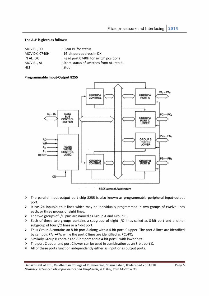
Programmable Input-Output 8255
� The parallel input-output port chip 8255 is also known as programmable peripheral input-output
port.
� It has 24 input/output lines which may be individually programmed in two groups of twelve lines
each, or three groups of eight lines.
� The two groups of I/O pins are named as Group A and Group B.
� Each of these two groups contains a subgroup of eight I/O lines called as 8-bit port and another
subgroup of four I/O lines or a 4-bit port.
� Thus Group A contains an 8-bit port A along with a 4-bit port, C upper. The port A lines are identified
by symbols PA0 –PA7 while the port C lines are identified as PC4-PC7.
� Similarly Group B contains an 8-bit port and a 4-bit port C with lower bits.
� The port C upper and port C lower can be used in combination as an 8-bit port C.
� All of these ports function independently either as input or as output ports.
Page 7
Microprocessors and Interfacing 2015
Department of ECE, Vardhaman College of Engineering, Shamshabad, Hyderabad - 501218 Page 7
Courtesy: Advanced Microprocessors and Peripherals, A.K. Ray, Tata McGraw Hill
� This can be achieved by programming the bits of internal register of 8255 called as Control Word
Register.
� The 8-bit data bus buffer is controlled by read/write control logic.
� The read/write control logic manages all of the internal and external transfer of both data and
control words.
Modes of Operation of 8255
� There are two basic modes of operation of 8255- I/O mode and Bit Set-Reset mode(BSR).
� In the I/O mode, the 8255 ports work as programmable I/O ports, while in BSR mode only port
C(PC0-PC7) can be used to set or reset its individual port bits.
� Under the IO mode of operation, further there are three modes of operation of 8255 so as to
support different types of applications- mode0, mode1 and mode2.
Bit Set-Reset Mode
� In this mode, any of the 8 bits of port C can be set or reset depending on B0 of the control word.
� The individual bits of port C can be set or reset by sending out a single OUT instruction to the control
register.
� When port C is used for control/status operation, this feature can be used to set or reset individual
bits.
� The bit to be set or reset is selected by bit select flags B3, B2 and B1 of the CWR.
BSR Mode Control Word Register Format
IO Modes
MODE 0: This mode is also known as basic input/output mode. This mode provides simple input and
output capability using each of the three ports.
The salient features of this mode are
1. Two 8 bit ports (port A and port B) and two 4-bits ports (port C upper and lower) are available.
The two 4-bit ports can be combinedly used as a third 8-bit port.
2. Any port can be used as an input and output port
3. Output ports are latched. Input ports are not latched.
4. A maximum of four ports are available so that overall 16 I/O configurations are possible.
Page 8
Microprocessors and Interfacing 2015
Department of ECE, Vardhaman College of Engineering, Shamshabad, Hyderabad - 501218 Page 8
Courtesy: Advanced Microprocessors and Peripherals, A.K. Ray, Tata McGraw Hill
All these modes can be selected by programming a register internal to 8255 known as Control Word
Register (CWR) which has two formats.
MODE 1: This mode is also known as strobed input/output mode. In this mode the handshaking signals
control the input or output action of the specified port.
The salient features of this mode are
1. Two groups- group A and group B are available for strobed data transfer.
2. Each group contains one 8-bit data I/O port and one 4-bit control/data port.
3. The 8-bit port can be either used as input or an output port.
4. Out of 8-bit port C, PC0-PC2 are used to generate control signals for port B and PC3-PC5 are used
to generate control signals for port A. the lines PC6,PC7 may be used as independent data lines.
MODE 2: This mode is also known as strobed Bidirectional input/output mode.
The salient features of this mode are
1. The single 8-bit port in group A is available.
2. The 8-bit port is bidirectional and additionally a 5-bit control port is available.
3. Three I/O lines are available at port C
4. Input and output ports are both latched
5. The 5-bit control port C is used for generating/accepting handshake signals for 8-bit data
transfer on port A.
Interfacing 8255 to 8086
Problem: Interface an 8255 with 8086 to work as an I/O port. Initialize port A as output port, port B as
input port and port C as output port. Port A address should be 0740H. Write a program to sense switch
positions SW0-SW7 connected to port B. the sensed pattern is to display on port A, to which 8 LEDs are
connected, while the port C lower displays number of on switches out of the total eight switches.
Solution:
Thus 82H is the control word for the requirements in the problem. The port address can be done as
given below.
Page 9
Microprocessors and Interfacing 2015
Department of ECE, Vardhaman College of Engineering, Shamshabad, Hyderabad - 501218 Page 9
Courtesy: Advanced Microprocessors and Peripherals, A.K. Ray, Tata McGraw Hill
� The 8255 is to be interfaced with lower order data bus, i.e. D0-D7
� The A0 and A1 pins of 8255 are connected to A01 and A02 pins of microprocessor respectively.
� The A00 pin of the microprocessor is used for selecting lower byte of data bus.
� Hence any change in the status of A00 does not affect the port to be selected.
� Let us use absolute decoding scheme that uses all the 16 address lines for deriving the device
address pulse.
� Out of A0-A15 lines, two address lines A02 and A01 are directly required by 8255 for three port and
CWR address decoding.
� Hence only A3 to A15 are used for decoding address.
Flow Chart
Page 10
Microprocessors and Interfacing 2015
Department of ECE, Vardhaman College of Engineering, Shamshabad, Hyderabad - 501218 Page 10
Courtesy: Advanced Microprocessors and Peripherals, A.K. Ray, Tata McGraw Hill
Program
MOV DX, 0746H ; Initialize CWR with
MOV AL, 82H ; control word 82H
OUT DX, AL ;
SUB DX, 04 ; Get address of port B in DX
IN AL, DX ; Read port B for switch
SUB DX, 02 ; positions in to AL and get port A address in DX
OUT DX, AL ; Display switch positions on port A
MOV BL, 00H ; Initialize BL for switch count
MOV CH, 08H
YY: ROL AL ; Rotate AL through carry to check,
JNC XX ; whether the switches are on or
INC BL ; off, i.e. either 1 or 0
XX: DEC CH ; Check for next switch. If all
JNZ YY ; switch are checked, the
MOV AL, BL ; number of on switches are
ADD DX, 04 ; in BL. Display it on port C
OUT DX, AL ; lower
HLT
Interfacing to Keyboard
� In most keyboards, the key switches are connected in a matrix of rows and columns.
� We use simple mechanical switches but the principle is same for other types of switches.
� Getting a meaningful data from a keyboard requires three major tasks.
1. Detect a key press.
2. Debounce the key press
3. Encode the key press
� The three tasks can be done with hardware, software, or a combination of two depending on
application.
Problem: Interface a 4*4 keyboard with 8086 using 8255 and write an ALP for detecting a key closure
and return the key code in AL. The debouncing period for a key is 10ms. Use software key debouncing
technique. DEBOUNCE is an available 10ms delay routine.
Solution:
� Port A is used as output port for selecting a row of key while port B is used as an input port for
sensing a closed key.
� Thus keyboard lines are selected one by one through port A and the port B lines are polled
continuously till a key closure is sensed.
� Then routine DEBOUNCE is called for debouncing.
� The key code is decided depending upon the selected row and a low sensed column.
� The higher order lines of port A and port B are left unused.
� The address of port A and port B will be respectively 8000H and 8002H while the address of CWR
will be 8006H.
Page 11
Microprocessors and Interfacing 2015
Department of ECE, Vardhaman College of Engineering, Shamshabad, Hyderabad - 501218 Page 11
Courtesy: Advanced Microprocessors and Peripherals, A.K. Ray, Tata McGraw Hill
Flow chart:
Page 12
Microprocessors and Interfacing 2015
Department of ECE, Vardhaman College of Engineering, Shamshabad, Hyderabad - 501218 Page 12
Courtesy: Advanced Microprocessors and Peripherals, A.K. Ray, Tata McGraw Hill
Check 1: whether any key is pressed or not?
1. Make all column lines zero by sending low on all output lines. This activates all keys in the
keyboard matrix.
2. Read the status of return lines. If status of all lines is logic high, key is not pressed; otherwise
pressed.
Check 2:
1. Activate keys from any one column by making any one column line zero.
2. Read the status of return lines. The zero on any return line indicates key is pressed from the
corresponding row and selected column.
3. Activate the keys from next column and repeat 2 and 3 for all columns.
Program:
ASSUME CS: CODE
CODE SEGMENT
START: MOV AL, 82H ; Load CWR with
MOV DX, 8006H ; control word
OUT DX, AL ; required
MOV BL, 00H ; Initialize BL for key code
XOR AX, AX ; Clear all flags
MOV DX, 8000H ; Port Address in AX
OUT DX, AL ; Ground all rows
ADD DX, 02 ; Port B address in DX
WAIT: IN AL, DX ; Read all columns
AND AL, 0F H ; Mask data lines D7-D4
CMP AL, 0F ; any key closed?
JZ WAIT ; if not, wait till key
CALL DEBOUNCE ; closure else wait for 10ms
MOV AL, F7 H ; Load data byte to ground
MOV BH, 04 H ; a row and set row counter
NXTROW: ROL AL, 01 H ; rotate AL to ground next row
MOV CH, AL ; save data byte to ground next row
SUB DX, 02 ; output Port address is in DX
OUT DX, AL ; ground one of the rows
ADD DX, 02 ; input port address is in DX
IN AL, DX ; read input for key closure
AND AL, 0F H ; mask D4-D7
MOV CL, 04 H ; set column counter
NXTCOL: ROR AL, 01 ; move D0 in CF
JNC CODEKY ; key closure is found, if CF=0
INC BL ; increment BL for next binary key code
DEC CL ; decrement column counter, if no key closure found
JNZ NXTCOL ; check for key closure key in next column
MOV AL, CH ; load data byte to ground next row
DEC BH ; if no key closure found in column get ready to ground next row
JNZ NXTROW ; go back to ground next row
JMP WAIT ; jump back to check for key closure again
CODEKY: MOV AL, BL ; key code is transferred to AL
MOV AH, 4C H ; return to DOS prompt
INT 21 H
Page 13
Department of ECE, Vardhaman College of Engineering, Shamshabad, Hyderabad
Courtesy: Advanced Microprocessors and Peripherals, A.K. Ray,
Procedure to generate 10ms delay at 5 MHz operating frequency
DEBOUNCE PROC NEAR
MOV CL, 0E2 H
BACK: NOP
DEC CL
JNZ BACK
RET
DEBOUNCE ENDP
CODE ENDS
END START
� Most of the microprocessor controlled instruments and mach
alphabet and numbers to give directions or data values to users.
� This can be displayed using CRT, LED or LCD displays.
� CRT displays are used when a large amount of data is to be displayed.
� In systems where only a small a
are used.
� 7 segment displays are generally used as numerical indicators and consists of a number of LEDs
arranged in seven segments.
� Any number between 0-
� The seven segments are labeled
� By forward biasing different LED segments, we can display the digits 0 through 9.
Problem: Interface an 8255 with 8086 at 80H as an I/O
displays with 8255. Write a sequence of instructions to display 1, 2, 3, 4 and 5 over five displays
continuously as per their positions starting with 1 at the least significant position.
Solution: In this scheme. I/O port A is multiplexed to carry data to all the 7
selects one of the displays at a time.
All these codes, decided above, are stored in a loo
Program:
ASSUME CS: CODE
CODE SEGMENT
AGAIN: MOV CL, 05H
MOV BX, 2000H
Microprocessors and Interfacing
ardhaman College of Engineering, Shamshabad, Hyderabad - 501218
Advanced Microprocessors and Peripherals, A.K. Ray, Tata McGraw Hill
nerate 10ms delay at 5 MHz operating frequency
Interfacing to Alphanumeric Displays
Most of the microprocessor controlled instruments and machines need to display letters of
alphabet and numbers to give directions or data values to users.
This can be displayed using CRT, LED or LCD displays.
CRT displays are used when a large amount of data is to be displayed.
In systems where only a small amount of data is to be displayed, simple LED and LCD displays
Interfacing to Seven Segment Displays
7 segment displays are generally used as numerical indicators and consists of a number of LEDs
arranged in seven segments.
-9 can be indicated by lighting the appropriate segments.
The seven segments are labeled as a-g and dot is labeled as h.
By forward biasing different LED segments, we can display the digits 0 through 9.
Interface an 8255 with 8086 at 80H as an I/O address of port A. interface five 7 segment
displays with 8255. Write a sequence of instructions to display 1, 2, 3, 4 and 5 over five displays
continuously as per their positions starting with 1 at the least significant position.
. I/O port A is multiplexed to carry data to all the 7-segment displays. The port B
selects one of the displays at a time. The displays used are common anode type.
All these codes, decided above, are stored in a look up table starting at 2000:0000
; Count for displays
; Initialize data segment
and Interfacing 2015
501218 Page 13
ines need to display letters of the
mount of data is to be displayed, simple LED and LCD displays
7 segment displays are generally used as numerical indicators and consists of a number of LEDs
9 can be indicated by lighting the appropriate segments.
By forward biasing different LED segments, we can display the digits 0 through 9.
address of port A. interface five 7 segment
displays with 8255. Write a sequence of instructions to display 1, 2, 3, 4 and 5 over five displays
continuously as per their positions starting with 1 at the least significant position.
segment displays. The port B
k up table starting at 2000:0000
Page 14
Microprocessors and Interfacing 2015
Department of ECE, Vardhaman College of Engineering, Shamshabad, Hyderabad - 501218 Page 14
Courtesy: Advanced Microprocessors and Peripherals, A.K. Ray, Tata McGraw Hill
MOV DS, BX ; for look up table
MOV CH, 01H ; 1st number to be displayed
MOV AL, 80H ; Load control word in the
OUT 86H, AL ; CWR
MOV DL, 01H ; Enable code for least significant 7-seg display
NXTDGT: MOV BX, 0000H ; Set pointer to look up table
MOV AL, CH ; First no to display Store number to be displayed in AL
XLAT ; Find code from look up table
OUT 80H, AL ; Display the code
MOV AL, DL ; Enable the display
OUT 82H, AL;
ROL DL ; Go for selecting next display
INC CH ; Next number to display
DEC CL
JNZ NXTDGT ; Go for next digit display
JMP AGAIN
CODE ENDS
Interfacing to Stepper Motor
� A stepper motor is a device used to obtain an accurate position control of rotating shafts.
� It employs rotation of its shafts in terms of steps, rather than continuous rotation as in case of
AC or DC motors.
� To rotate the shafts of the stepper motor, a sequence of pulses is needed to be applied to the
windings of the stepper motor in a proper sequence.
� The numbers of pulses required for one complete rotation of the shaft of the stepper motor are
equal to its number of internal teeth or its rotor.
� A typical stepper motor may have parameters like torque 3Kg-cm, operating voltage 12V,
current rating 0.2A and a step angle 1.80, i.e. 200 steps/revolution (number of rotor teeth).
� A simple scheme for rotating the shaft of stepper motor is called a wave scheme.
Page 15
Microprocessors and Interfacing 2015
Department of ECE, Vardhaman College of Engineering, Shamshabad, Hyderabad - 501218 Page 15
Courtesy: Advanced Microprocessors and Peripherals, A.K. Ray, Tata McGraw Hill
� In this scheme, the windings Wa, Wb, Wc and Wd are applied with required voltage pulses, in a
cyclic fashion.
Problem: Design a stepper motor controller and write an ALP to rotate shaft of 4-phase stepper motor:
a. In clock wise 5 rotations
b. In anticlockwise 5 rotations
The 8255 port A address is 0740H. The stepper motor has 200 rotor teeth. The port A bit PA0 drives
winding Wa, PA1 drives Wb and so on. The stepper motor has an inertial delay of 10ms. Assume that the
routine for this delay is already available.
Solution: The stepper motor connections for all the four windings are
Program:
ASSUME CS: CODE
CODE SEGMENT
START: MOV AL, 80H
OUT CWR, AL
MOV AL, 88H ; Bit pattern 10001000 to start the sequence of excitation from Wa.
MOV CX, 1000 ; for clockwise rotations the count is 200*5=1000
AGAIN1: OUT PORTA, AL ;
CALL DELAY ; Excite Wa, Wb, Wc, Wd in sequence with delay.
ROL AL, 01 ;
DEC CX ;
JNZ AGAIN1 ; Excite till count=0
MOV AL, 88H ; Bit pattern to excite Wa
MOVCX, 1000 ; count for 5 rotations
AGAIN2: OUT PORTA, AL ; excite Wa, Wb, Wc, Wd
CALL DELAY ; Wait
ROR AL, 01 ; anticlockwise
Page 16
Microprocessors and Interfacing 2015
Department of ECE, Vardhaman College of Engineering, Shamshabad, Hyderabad - 501218 Page 16
Courtesy: Advanced Microprocessors and Peripherals, A.K. Ray, Tata McGraw Hill
DEC CX
JNZ AGAIN2
MOV AH, 4CH
INT 21H
CODE ENDS
END START
Interfacing to A/D Converter
A general algorithm for ADC interfacing contains:
1. Ensure the stability of analog input applied to the ADC
2. Issue start of conversion (SOC) pulse to ADC
3. Read end of conversion (EOC) signal to mark the end of conversion process
4. Read digital data output of the ADC as equivalent digital output
It may be noted that the analog input voltage must be a constant at the input of the ADC right from the
beginning to end of the conversion to get correct results.
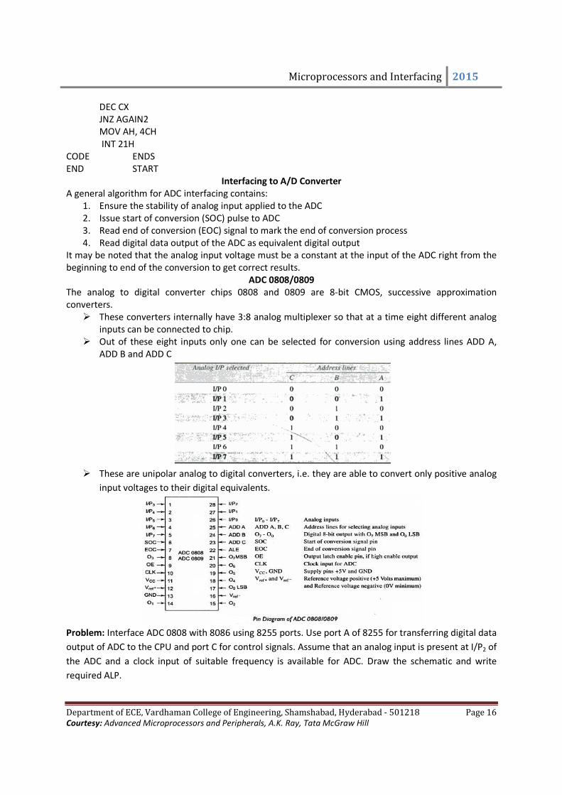
ADC 0808/0809
The analog to digital converter chips 0808 and 0809 are 8-bit CMOS, successive approximation
converters.
� These converters internally have 3:8 analog multiplexer so that at a time eight different analog
inputs can be connected to chip.
� Out of these eight inputs only one can be selected for conversion using address lines ADD A,
ADD B and ADD C
� These are unipolar analog to digital converters, i.e. they are able to convert only positive analog
input voltages to their digital equivalents.
Problem: Interface ADC 0808 with 8086 using 8255 ports. Use port A of 8255 for transferring digital data
output of ADC to the CPU and port C for control signals. Assume that an analog input is present at I/P2 of
the ADC and a clock input of suitable frequency is available for ADC. Draw the schematic and write
required ALP.
Page 17
Microprocessors and Interfacing 2015
Department of ECE, Vardhaman College of Engineering, Shamshabad, Hyderabad - 501218 Page 17
Courtesy: Advanced Microprocessors and Peripherals, A.K. Ray, Tata McGraw Hill
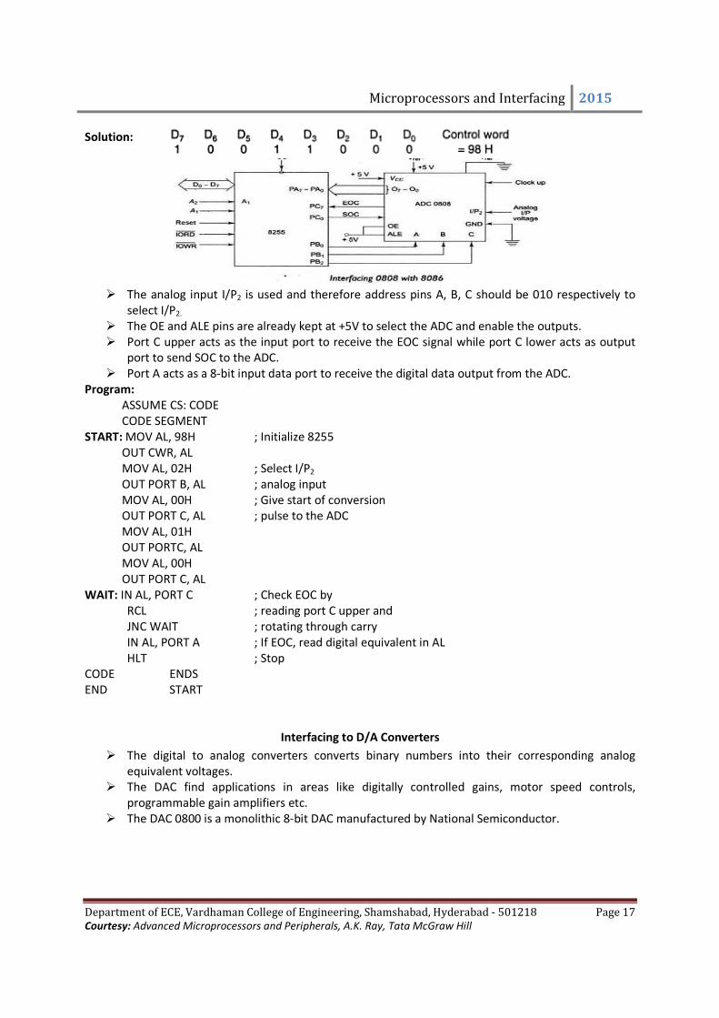
Solution:
� The analog input I/P2 is used and therefore address pins A, B, C should be 010 respectively to
select I/P2.
� The OE and ALE pins are already kept at +5V to select the ADC and enable the outputs.
� Port C upper acts as the input port to receive the EOC signal while port C lower acts as output
port to send SOC to the ADC.
� Port A acts as a 8-bit input data port to receive the digital data output from the ADC.
Program:
ASSUME CS: CODE
CODE SEGMENT
START: MOV AL, 98H ; Initialize 8255
OUT CWR, AL
MOV AL, 02H ; Select I/P2
OUT PORT B, AL ; analog input
MOV AL, 00H ; Give start of conversion
OUT PORT C, AL ; pulse to the ADC
MOV AL, 01H
OUT PORTC, AL
MOV AL, 00H
OUT PORT C, AL
WAIT: IN AL, PORT C ; Check EOC by
RCL ; reading port C upper and
JNC WAIT ; rotating through carry
IN AL, PORT A ; If EOC, read digital equivalent in AL
HLT ; Stop
CODE ENDS
END START
Interfacing to D/A Converters
� The digital to analog converters converts binary numbers into their corresponding analog
equivalent voltages.
� The DAC find applications in areas like digitally controlled gains, motor speed controls,
programmable gain amplifiers etc.
� The DAC 0800 is a monolithic 8-bit DAC manufactured by National Semiconductor.
Page 18
Microprocessors and Interfacing 2015
Department of ECE, Vardhaman College of Engineering, Shamshabad, Hyderabad - 501218 Page 18
Courtesy: Advanced Microprocessors and Peripherals, A.K. Ray, Tata McGraw Hill
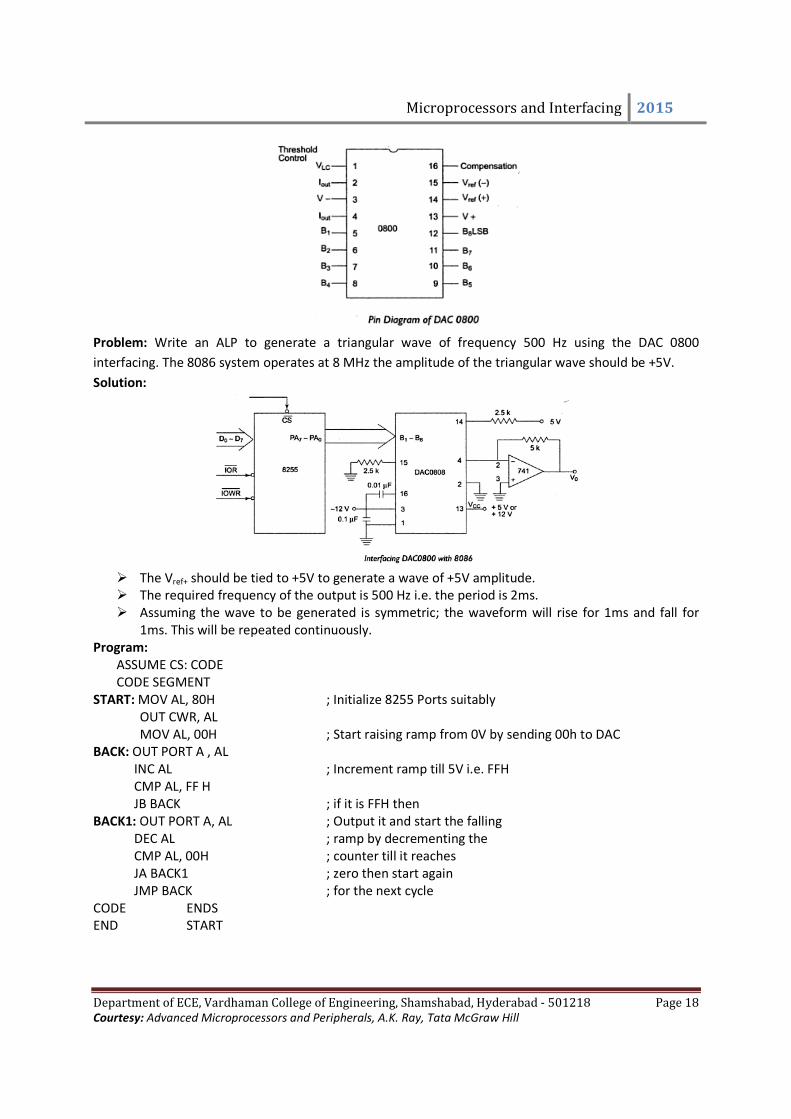
Problem: Write an ALP to generate a triangular wave of frequency 500 Hz using the DAC 0800
interfacing. The 8086 system operates at 8 MHz the amplitude of the triangular wave should be +5V.
Solution:
� The Vref+ should be tied to +5V to generate a wave of +5V amplitude.
� The required frequency of the output is 500 Hz i.e. the period is 2ms.
� Assuming the wave to be generated is symmetric; the waveform will rise for 1ms and fall for
1ms. This will be repeated continuously.
Program:
ASSUME CS: CODE
CODE SEGMENT
START: MOV AL, 80H ; Initialize 8255 Ports suitably
OUT CWR, AL
MOV AL, 00H ; Start raising ramp from 0V by sending 00h to DAC
BACK: OUT PORT A , AL
INC AL ; Increment ramp till 5V i.e. FFH
CMP AL, FF H
JB BACK ; if it is FFH then
BACK1: OUT PORT A, AL ; Output it and start the falling
DEC AL ; ramp by decrementing the
CMP AL, 00H ; counter till it reaches
JA BACK1 ; zero then start again
JMP BACK ; for the next cycle
CODE ENDS
END START


![[XLS] · Web viewKapas Hera Tarikere Chowtuppal Shamshabad Bhongir Kama Reddy Zaheerabad Kattingeri Deralakatte Ujire Bhemunipatnam-Tagarapuvalasa Parvathipuram Ramabhadrapuram S.Kota](https://static.documents.pub/doc/80x56/5aea20a27f8b9a3b2e8c36ac/xls-viewkapas-hera-tarikere-chowtuppal-shamshabad-bhongir-kama-reddy-zaheerabad.jpg)


