26
04.07.2006 Seite: 1 Semiconductor Packaging for High Power Diode Lasers
| Date post: | 16-Mar-2018 |
| Category: |
Documents |
| Upload: | hoangthuan |
| View: | 218 times |
| Download: | 2 times |

04.07.2006 Seite: 1
Semiconductor Packaging for
High Power Diode Lasers
04.07.2006 Seite: 2
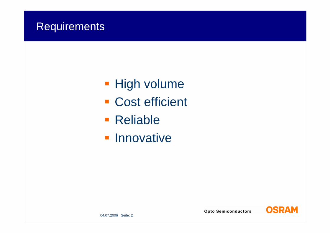
Requirements
High volumeCost efficientReliableInnovative

04.07.2006 Seite: 3
Considerations
Mechanicaldifferent materials with distinct properties at different conditions (-40°C…+125°C)Electricalhigh current at low voltage or internal conversionOpticalhigh intensity light source needs low/zero absorption materialsEconomicalthe concept must work and must be affordable

04.07.2006 Seite: 4
Examples
Smart laser.pulse laser for peak pulses up to P=100W withinternal driver circuit
ACC - pulse laser modulepulse laser-bar with 12 channels on PCB for SMT packaging
Sirilas®cw-laser module on TO263 lead-frame technology
04.07.2006 Seite: 5
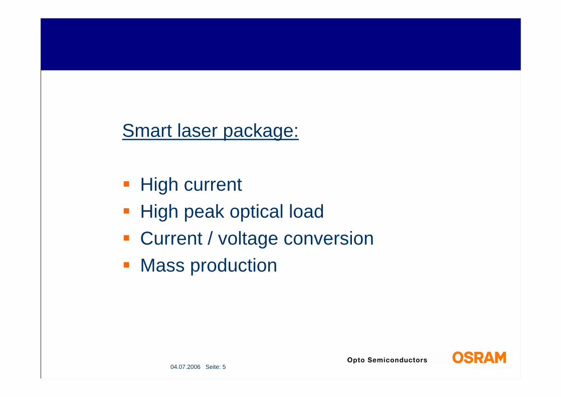
Smart laser package:
High currentHigh peak optical loadCurrent / voltage conversionMass production

04.07.2006 Seite: 6
Smart laser – general performance
70
80
90
100
110
0 250 500 750 1000
time [h]
Pop
t_de
t [%
] .
h 80 W @ 100° C ambient temp.
h hardly any degradation at high power level and high temperature
50
75
100
-25 25 75 125T [°C]
P [W
] 50A
Pw = 50 ns
ν = 1 kHz

04.07.2006 Seite: 7
Smart laser - components
Lead frame
Laser chipCapacitorsFET

04.07.2006 Seite: 8
Smart laser - die bonding
Laser die
FET
Capacitor for charge acc
Capacitor for charge acc
Die bonding: - standard process,- uses often conductive glue- high throughput and highly automized
04.07.2006 Seite: 9
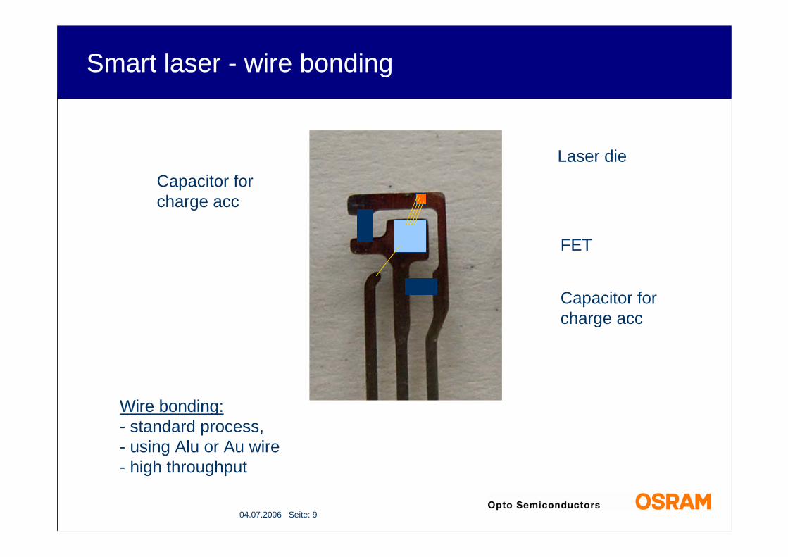
Smart laser - wire bonding
Laser die
FET
Capacitor for charge acc
Capacitor for charge acc
Wire bonding: - standard process,- using Alu or Au wire- high throughput

04.07.2006 Seite: 10
Smart laser - casting
Casting:Resin needs to grant: protection
against mechanical forcesagainst humidityagainst solvents
while offering good light output andgood stability at all temperatureswithout damaging device and package
Lead frame afterdie and wire bonding
Casting form filledwith resin

04.07.2006 Seite: 11
Smart laser - singulation and testingLL90_3
3 samples, Lot 01-17-01, 30ns, 1kHz, 25°C
0
10
20
30
40
50
60
70
80
0 5 10 15 20 25 30 35
Charge Voltage, V
Opt
ical
Pow
er, W
1
2
3
Singulation (after casting) and testing. Depicted is a measurement that showsthat the laser is operated at high voltage
Finished package after casting

04.07.2006 Seite: 12
Package for pulse laser array:
High currentHigh optical loadMultiple channelAutomotive qualification

04.07.2006 Seite: 13
Application: Laser range finder
Detects distance and velocity relative to thecar driving ahead⇒ Enables automatic Save Distance control⇒ Range 100 - 200 m
0
40
80
120
0 10 20 30 40 50current [A]
Pea
k-P
ower
[W] 3
2
1
04.07.2006 Seite: 14
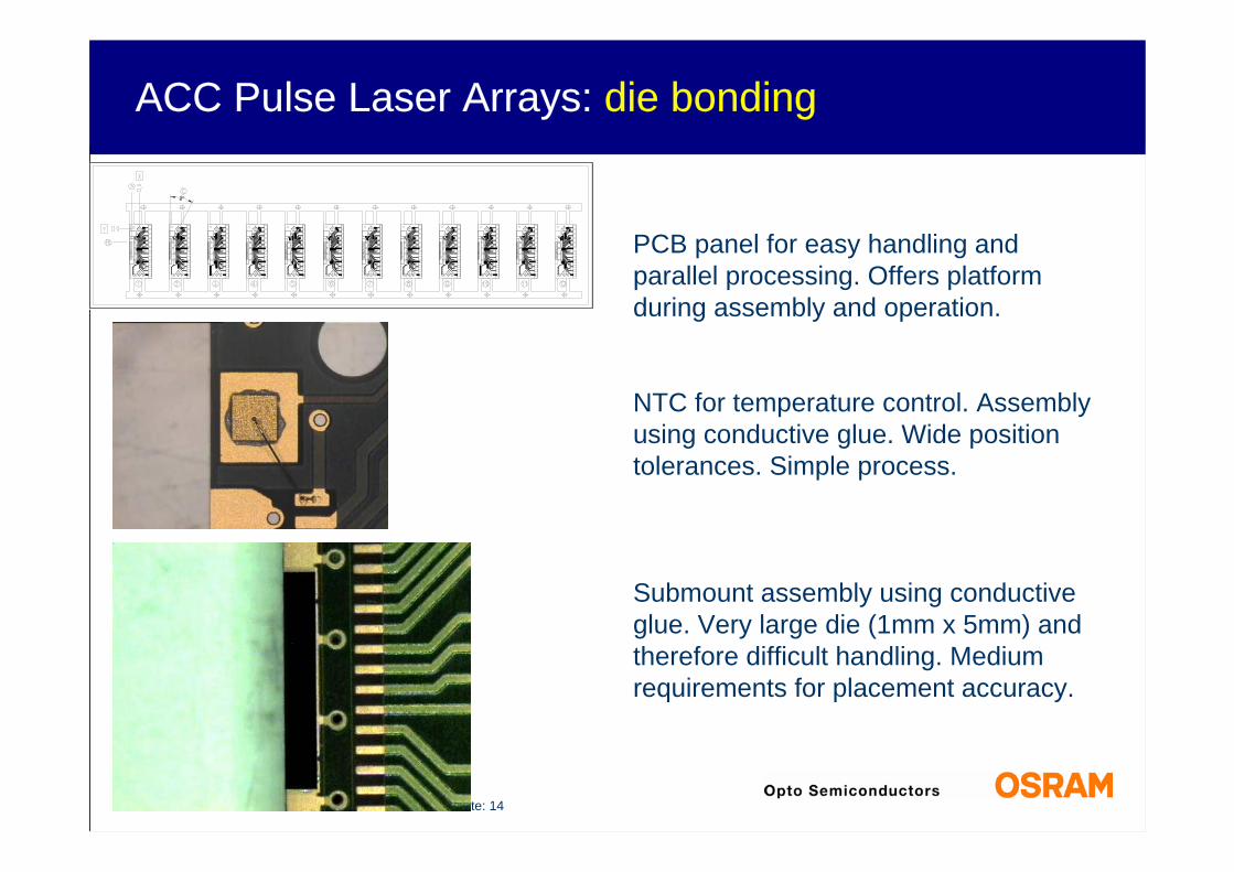
ACC Pulse Laser Arrays: die bonding
PCB panel for easy handling and parallel processing. Offers platformduring assembly and operation.
NTC for temperature control. Assemblyusing conductive glue. Wide positiontolerances. Simple process.
Submount assembly using conductiveglue. Very large die (1mm x 5mm) andtherefore difficult handling. Medium requirements for placement accuracy.
04.07.2006 Seite: 15
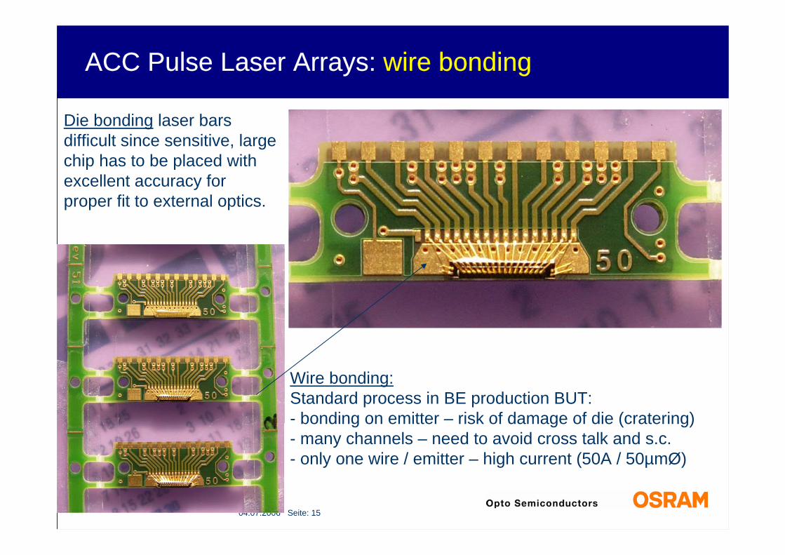
ACC Pulse Laser Arrays: wire bonding
Die bonding laser barsdifficult since sensitive, large chip has to be placed withexcellent accuracy forproper fit to external optics.
Wire bonding:Standard process in BE production BUT:- bonding on emitter – risk of damage of die (cratering)- many channels – need to avoid cross talk and s.c.- only one wire / emitter – high current (50A / 50µmØ)

04.07.2006 Seite: 16
ACC Pulse Laser Arrays: housing and separation
Housing assembly:Gluing PCB to housing. Risc of damaging die or wire bonds.
Punching of PCB for separation of individual units out of frame. Riscof bending PCB and loosing glueinterface
Fit housing – PCB:Tight fit requires tight specificationsand tight manufacturing specs for housing and PCB mechanicalinterfaces: Holes in PCB and postsin housing
Tracing:For later reference, all samples must betraceable. Therefore logisticdrops in at this working step.
04.07.2006 Seite: 17
Package for CW Laser:
High heat loadHigh currentHigh optical load

04.07.2006 Seite: 18
Application: Hardening
2 x 1.5 kW
99% availability
04.07.2006 Seite: 19
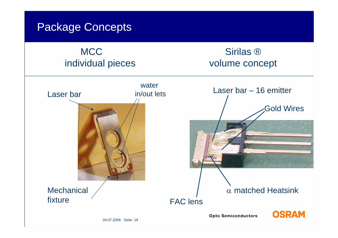
Package Concepts
FAC lensα matched Heatsink
Laser bar – 16 emitter
Gold Wires
MCC Sirilas ®individual pieces volume concept
Laser bar
Mechanical fixture
waterin/out lets

04.07.2006 Seite: 20
Interfaces : Current, heat, light
Drive current:35 .. 40 A @ 2 V
Optical outputpower:up to 30W cwNA < 0.1
Thermal load: 40 to 50 W Rth ≈ 0,6 K/W
Water cooling

04.07.2006 Seite: 21
Package Technology
High temperaturepremold TO263 type leadframe
Laserbar
Heatsink
Cylindrical lens
04.07.2006 Seite: 22
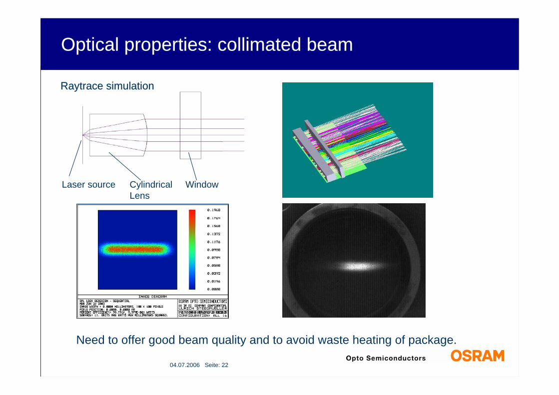
Optical properties: collimated beam
Laser source CylindricalLens
Window
Raytrace simulation
Need to offer good beam quality and to avoid waste heating of package.

04.07.2006 Seite: 23
Assembly: die and wire bonding
After wire bonding and lens assemblyDie bonding:
Wire bonding:
Laser bar lens

04.07.2006 Seite: 24
• ITH = 8.4 A
• η = 1.28 W/A
• RS = 4,4 mΩ
6.4mm Laser bar @ 50 W opt power: • IOP = 48,5 A• UOP = 1.81 V• WPE = 58.6 %
L-I-V characteristics
0
0,4
0,8
1,2
1,6
2
2,4
0 10 20 30 40 50Current, A
Vol
tage
/ V
0
10
20
30
40
50
60
Pow
er /
W; W
PE
/ %

04.07.2006 Seite: 25
Reliability: Intermittent CW
0,0
0,2
0,4
0,6
0,8
1,0
1,2
0,0 4,0 8,0 12,0 16,0 20,0 24,0 28,0 32,0 36,0 40,0
MShot
Popt
[nor
m.]
Wear out failures ( Degradation ) t50% = 62 MShotRandom failures with. open contact not seen yet
Iop=0A..36A
Using hard solder and CTE matched submount reduces stress and allows for excellent reliability. Up to now, no spontaneous failure.

04.07.2006 Seite: 26
Summary
Diode lasers are used for many distinct applications(sensing, illumination, direct application…)
They operate in a very wide range of environmentalconditions (-40°C….+125°C, humidity, …)
Different kind of packages have been developed(high volume, highly specialized, optics, SMT….) for optimal use of die capabilties.


