Order this document by AN1739/D Semiconductor Products Sector Application Note AN1739 A/D Conversion Software for the MC68HC05JJ/JP Series Microcontrollers By Mark L. Shaw Member, Technical Staff Phoenix, Arizona Introduction The MC68HC05JJ/JP series of microcontrollers (MCUs) can be used to build simple single slope analog-to-digital (A/D) converters of up to 12-bits of measurement. The intent of this application note is to present a set of software examples for the MC68HC05JJ/JP using each of the four modes of operation. Additional information on the analog subsystem of these MCUs can be found in Applications Using the Analog Subsystem on MC68HC05JJ/JP Series Microcontrollers, Freescale Freescale Semiconductor, I For More Information On This Product, Go to: www.freescale.com nc...
Transcript
Order this documentby AN1739/D
Fre
esc
ale
Se
mic
on
du
cto
r, I
nc
...
Semiconductor Products SectorApplication Note
AN1739
A/D Conversion Software for theMC68HC05JJ/JP Series Microcontrollers
By Mark L. ShawMember, Technical StaffPhoenix, Arizona
Introduction
The MC68HC05JJ/JP series of microcontrollers (MCUs) can be used to build simple single slope analog-to-digital (A/D) converters of up to 12-bits of measurement. The intent of this application note is to present a set of software examples for the MC68HC05JJ/JP using each of the four modes of operation. Additional information on the analog subsystem of these MCUs can be found in Applications Using the Analog Subsystem on MC68HC05JJ/JP Series Microcontrollers, Freescale
For More Information On This Product, Go to: www.freescale.com
rxzb30
ForwardLine
rxzb30
fslcopyrightline
rxzb30
freescalecolorjpeg
Application Note
F
ree
sca
le S
em
ico
nd
uc
tor,
I
Freescale Semiconductor, Inc.n
c..
.
Analog-to-Digital Conversion
Analog-to-digital conversion can be accomplished using the JJ/JP-series by allowing the current source to charge up (ramp) an integration capacitor connected to PB0 and use comparator 2 to detect the time when the ramp voltage crosses the unknown voltage being measured as shown in Figure 1.
Figure 1. Single Slope A/D Convertor
+
–
PB0
VDD
AN0
ICHG
PBX
VCAP
VX
ON
CMP2+
–
PB0
VDD
AN0
IDISCHG
PBX
VCAP
VX
ON
CMP2
VX
VCAPVSS
CHG
CHARGE
CHARGE (CHG = 1)
DISCHARGE
DISCHARGE (CHG = 0)
OFF
OFF
CMP2
AN1739
2 For More Information On This Product,
Go to: www.freescale.com
Application NoteAnalog-to-Digital Conversion
F
ree
sca
le S
em
ico
nd
uc
tor,
I
Freescale Semiconductor, Inc.n
c..
.
Performance Calculations
Fundamental to the single slope A/D conversion technique is the following equation relating time to voltage dependent on the external ramping capacitor and its charging current:
where:
tCHG = Charge time (seconds)
VX = Voltage to reach (volts)
CEXT = External ramp capacitor (µF)
ICHG = Charge current (µA)
From this basic equation the time can be translated into a number of counts at a given frequency:
where:
tFS = Full scale charge time (seconds)
NFS = Full scale counts (counts)
P = Prescaler (counts out/counts in)
fOSC = Oscillator frequency (Hz)
CEXT = External ramp capacitor (µF)
tCHG =CEXT × Vx
ICHG
tFS =P × NFS
fOSC
CEXT × VFS
ICHG=
For More Information On This Product,
Go to: www.freescale.com
Application Note
F
ree
sca
le S
em
ico
nd
uc
tor,
I
Freescale Semiconductor, Inc.n
c..
.
Step-By-Step A/D Conversion
After selecting the right components, the single slope A/D can be operated as a series of simple software controlled steps:
1. Initialize the analog subsystem to the desired configuration.
2. Discharge the internal sample capacitor and channel select bus.
3. Select a signal source.
4. Start charging the ramp capacitor (set CHG bit in ACR)
5. Keep track of time while waiting for comparator 2 output to go high.
6. Capture time when comparator 2 output goes high.
7. Start discharging the ramp capacitor (clear CHG bit in ACR)
8. Calculate the charge time.
9. Compare the charge time to that for a reference signal.
10. When the ramp capacitor is fully discharged, go back to step 3.
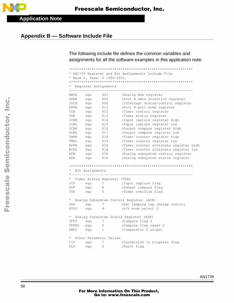
Analog Subsystem Registers
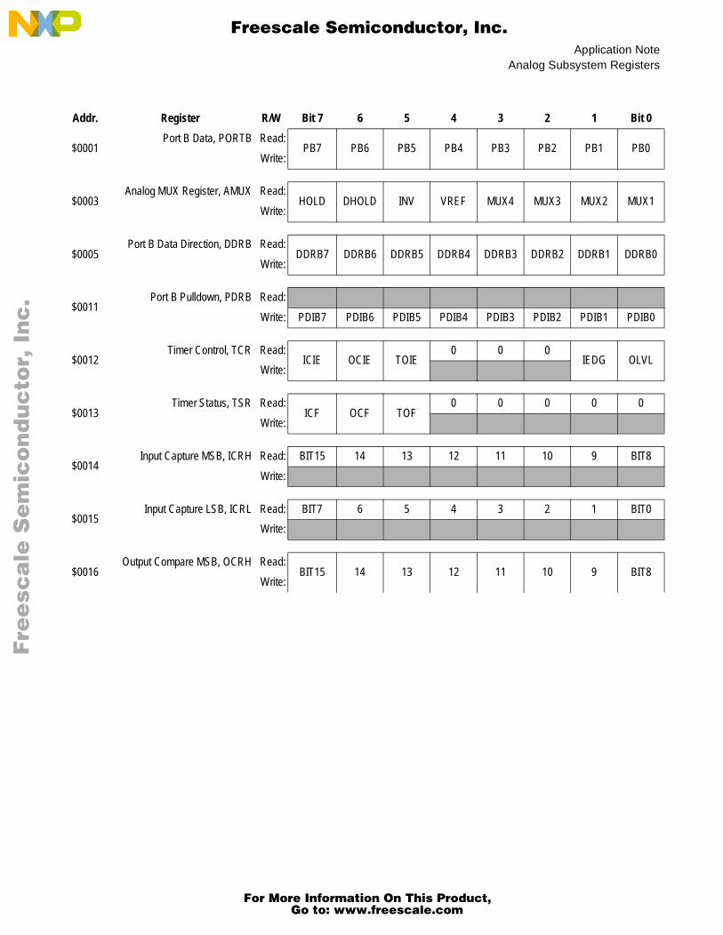
The analog subsystem is structured around several basic components: a pair of voltage comparators and a constant current source which are controlled and monitored by the analog MUX register (AMUX) at $0003, the analog control register (ACR) at $001D, and the analog status register (ASR) at $001E. All the registers relating to the analog subsystem are shown in Figure 2.
Single slope A/D conversion has six unwanted faults near the limits of its input voltage range, in the signal noise, and timing with respect to the software. The user should check their application to see if any of these faults are possible. These faults are described briefly here with further detail available from Applications Using the Analog Subsystem on MC68HC05JJ/JP Series Microcontrollers, Freescale document order number AN1740/D.
Infinite Conversion Time
When the unknown input signal is above the common-mode range of comparator 2 the integration ramp on the PB0 pin can never reach the level to trip comparator 2 and set the CPF2 flag.
Disabled Conversion A/D Fault
The CPF2 flag bit is set by a rising transition on the output of comparator 2. If the output of comparator 2 cannot return to the low state this flag bit cannot get set indefinitely. This occurs if the PB0 pin cannot be discharged below the level on the negative input to comparator 2.
Extra Conversion A/D Fault
When the PB0 pin has been discharged and the input voltage is near VSS the presence of noise on either the measured input voltage or the PB0 pin can cause comparator 2 to switch and the CPF2 flag bit will be set even though there is no conversion ramp in progress.
Early ConversionA/D Fault
When the conversion time is long there exists the possibility for noise on either the input signal or the PB0 ramping voltage to cause comparator 2 to trip the CPF2 flag earlier than would normally have occurred.
Conversion Overlap A/D Fault
When the conversion time becomes too long in mode 0 or 1 the software is still looping on the conversion and no subsequent events can occur. But in mode 2 or 3 a very long conversion could overlap the next TOF or OCF which is trying to start another conversion. The net result will be
AN1739
6 For More Information On This Product,
Go to: www.freescale.com
Application NoteManual A/D Conversions (Modes 0 and 1)
F
ree
sca
le S
em
ico
nd
uc
tor,
I
Freescale Semiconductor, Inc.n
c..
.
that an ICF for the first conversion may appear associated with the start of the second conversion. This fault is only associated with mode 2 or 3.
Conversion Masking A/D Fault
In mode 0 or 1 the software handles all the events in an established subsequence such that simultaneous events do not happen. But in mode 2 or 3 an unwanted conversion fault may make an ICF occur near the same time as the TOF or OCF which is trying to start another conversion. Such an unwanted ICF just before the TOF cannot be discerned from a true ICF that would occur if the input voltage were near VSS. This fault is only associated with mode 2 or 3.
Manual A/D Conversions (Modes 0 and 1)
Mode 0 or 1 conversions are completely under the control of the software and therefore are slow compared to hardware timing. All events are therefore predictable and occur in a known sequence.
The main limitation of modes 0 and 1 is that the timing will be slower either due to software timing loops or slower accesses to the 16-bit timer or multifunction timer. Therefore, modes 0 or 1 are usually limited to 8-bit conversions unless extremely long conversion times can be tolerated in the application.
For More Information On This Product,
Go to: www.freescale.com
Application Note
F
ree
sca
le S
em
ico
nd
uc
tor,
I
Freescale Semiconductor, Inc.n
c..
.
Timing via Timer Reads
Timing of the conversion can be done by reading the state of the 16-bit timer or the multifunction timer. The software must account for the delays in reading these registers and the asynchronous clocking of these timers with respect to the instruction cycles. These sources of timing “jitter” will degrade the accuracy of the readings.
Analog Interrupt Timing
The conversion can be timed with a combination of software start of the charging ramp and an analog interrupt which reads the 16-bit timer or multifunction timer. This mode of operation will allow other tasks to be performed while the conversion is in progress, which is especially useful for very long conversions. However, the accuracy of the analog interrupt being able to capture the ending time means that all other interrupts may not be active until after the conversion is complete.
Also, once the analog interrupt is entered, the time that is read must be corrected for the minimum interrupt latency time to get into the analog interrupt service routine and read the timer state. This latency, and therefore the accuracy of the time, will be affected by the variation in cycle times of all instruction types used in the particular application software. Avoiding long cycle time instructions such as JSR, SWI, MUL, and some indexed addressing modes can reduce this variation from 9 to 3 bus cycles.
Automated A/D Conversions (Modes 2 and 3)
Mode 2 and 3 conversions are mostly under the control of the 16-bit timer, but need occasional maintenance to keep flags cleared and transfer input capture times to RAM for use by other routines. Due to the more accurate start and stop timing and high possible bit counts, mode 2 or 3 conversions are best for conversions of more than 8 bits.
Mode 2 or 3 conversions use the timer overflow flag (TOF) or the output compare flag (OCF) and the input capture flag (ICF) of the 16-bit timer to control the charging of the integration capacitor connected to PB0.
AN1739
8 For More Information On This Product,
Go to: www.freescale.com
Application NoteAutomated A/D Conversions (Modes 2 and 3)
F
ree
sca
le S
em
ico
nd
uc
tor,
I
Freescale Semiconductor, Inc.n
c..
.
When using these timer flags the designer should be aware of the following behaviors:
1. The TOF flag bit is set whenever the 16-bit timer counter overflows from $FFFF to $0000 regardless of whether or not the timer overflow interrupt is enabled (TOIE bit set in TCR).
a. Once set, the TOF bit must be reset by the proper software sequence of reading the TSR, then the TMRL.
b. Since the timer starts with $FFFC after a reset of the MCU a TOF will occur almost immediately following a reset.
2. The OCF flag bit is set whenever the 16-bit timer counter matches the count stored into the output compare registers regardless of whether or not the timer output compare interrupt is enabled (OCIE bit set in TCR).
a. Once set, the OCF bit must be reset by the proper software sequence of reading the TSR, then the OCRL.
b. Once set, the OCF will lock out any future compares until the OCF flag bit is cleared.
c. An OCF can occur at any time following a reset since the contents of the OCRL and OCRH are unaffected by a reset.
3. The ICF flag bit is set whenever an input capture is received by the 16-bit timer regardless of whether or not the timer input capture interrupt is enabled (ICIE bit set in TCR).
a. Once set, the ICF bit must be reset by the proper software sequence of reading the TSR, then the ICRL.
b. Once set, the ICF will lock out any future input captures until the ICF flag bit is cleared.
c. In the control of the analog current source the ICF flag overrides the TOF or OCF flags. If an TOF or OCF is present when the ICF is cleared, the charging of the PB0 pin will begin immediately.
d. The ICF can be triggered by a positive or negative going edge depending on the state of the IEDG bit in the TCR.
e. The trigger source for the ICF can be either the signal on PB3 or the output of voltage comparator 2 dependent on the state of the ICEN bit in the ACR.
AN1739
9 For More Information On This Product,
Go to: www.freescale.com
Application Note
F
ree
sca
le S
em
ico
nd
uc
tor,
I
Freescale Semiconductor, Inc.n
c..
.
The most important considerations in using the automated modes 2 or 3 is that the TOF, OCF, and ICF flags can get set without any enabling control; and that following a reset they can get set before the software is ready to use them. This means that modes 2 or 3 can operate as either interrupt driven or free-running software. The following examples for mode 2 or 3 A/D conversions take into account these factors.
Use of Conversion Flags
It is highly recommended that modes 2 and 3 use conversion status flags such as EOC (for end-of-conversion) and CIP (for conversion-In-progress). These flags allow the timer interrupt service routine to determine if the conversions are executing properly or a fault has occurred. These flags should be contained in an assigned RAM location. Avoid using the CHG bit in the ACR or the CPF2 or CMP2 bits in the ASR for these purposes since they can be set automatically by hardware events that are not under the user’s direct software control.
Value of the Captured Times
The biggest advantage of modes 2 and 3 is that the start time of the conversion is clearly defined by the TOF of OCF timer state and the end of conversion is captured precisely by the ICF. Therefore, the software sequence and cycle times are not critical to the timing accuracy. The only concern should be that the ICF is combined with the correct TOF of OCF that started the conversion ramp. Also the software must access the proper values and clear the flags before the next conversion is to begin. This allows more latitude in defining error checks than is possible with modes 0 or 1 which are sensitive to software cycle timing.
Correct Mode Initialization
The initialization of either mode 2 or 3 must be done at the proper time since the TOF or OCF flags may become set before the mode can be established. If the TOF is already set and mode 2 is initiated, then the charge ramp will begin immediately without regard for when the TOF actually occurred. Similarly, the OCF could be set before mode 3 is initialized. It is important that the TOF and ICF flags be clear before the mode 2 is established; or that the OCF and ICF flags be clear before the mode 3 is established. The best way to accomplish this is to wait for the first TOF in mode 2 or first OCF in mode 3, then clear all flags and finally set the ATD1 and ATD2 bits as required.
AN1739
10 For More Information On This Product,
Go to: www.freescale.com
Application NoteA/D Examples
F
ree
sca
le S
em
ico
nd
uc
tor,
I
Freescale Semiconductor, Inc.n
c..
.
A/D Examples
The following A/D conversion examples all use the include files from Appendix B — Software Include File for variables and the subroutines in Appendix C — General Subroutines Used in Examples.
A/D #1 — Mode 0
In this A/D example the device is placed in mode 0 and the current source is controlled by software to charge the PB0 pin while keeping a count in software. Results are stored as an 8-bit result in RAM. Code is added to test for any excessively long conversion times in case the input is undefined, out of the common range of the comparator, or at or below the VSS potential. This A/D conversion example will follow the basic flow chart given in Figure 3 and the listing given in Software Listing 1 — Mode 0 A/D Conversions.
The A/D cycle time is about 4.4 ms between maximum length conversions for a 0.1-µF capacitor and 2-MHz oscillator. Discharge time is about 0.8 ms. Full scale value of $FF occurs with an input voltage of about 3.5 volts for a 5-volt supply to VDD.
At first glance this may look like a lot of code to simply set the CHG bit and count time until the CMP2 bit goes high. But only 29 bytes do the actual A/D conversion subroutine. The conversion loop takes 14 CPU bus cycles which is equal to a prescaler of 28 with respect to the oscillator frequency, fOSC. The A/D conversion software also handles the possible faults described earlier. The software example provides for ideal sampling, where it is desirable to have the first test of the comparator output occur at 1/2 of the recurring cycle time or “bit time” of the conversion loop. Thus, the start of the charge ramp occurs on the 4th bus cycle of the BSET instruction and the first read of the comparator output occurs on the 3rd bus cycle of the BRSET instruction. The BRN instruction gives a three cycle delay for a total time from ramp start to first read of 7 bus cycles.
AN1739
11 For More Information On This Product,
Go to: www.freescale.com
Application Note
F
ree
sca
le S
em
ico
nd
uc
tor,
I
Freescale Semiconductor, Inc.n
c..
.
The A/D conversion is implemented as a subroutine which can be called as needed by the background routines. This allows the background routine to select the desired channel and use the conversion results as needed.
NOTE: It should be noted that some assemblers do not support the BRN instruction. In this case, insert a FDB $2100 which is the opcode for the BRN instruction ($21) plus a dummy offset ($00).
In mode 0 careful attention to the timing of read or write cycles should be done when controlling signals to the comparators or reading their output states. The information in Instruction Cycle Timing of MC68HC05JJ/JP Series Microcontrollers, Freescale document order number AN1738/D, indicates the time within the instruction where it actually reads or writes data.
jsr INIT0 ;Initialize analog subsystem;Set up oscillator
cli ;Enable interrupts, if used
************************************************************* MAKE A/D CONVERSIONS BY MONITORING COMPARATOR 2 OUTPUT* Ready to monitor comparator outputs and selected input* channel for comparator 2. *-----------------------------------------------------------BLOOP lda #%10000001 ;Select HOLD and MUX1
jsr ATDGO ;Go fetch A/D conversionsta DATA ; count in accumulator
ldx #$76 ;Wait 720 usec for dischargejsr TDELAY ; delay of 6 msec/uF. Delay
; not required if background; software time long enough.
lda #%10100001 ;Select HOLD, INV, and MUX1jsr ATDGO ;Go fetch A/D conversionsta IDATA ; count in accumulator
ldx #$76 ;Wait 720 usec for dischargejsr TDELAY ; delay of 6 msec/uF when
; using 0.12 uF. Delay; not required if background; software time long enough.
*-----------------------------------------------------------* NOTE: Inverted input and averaging may not be required for* some applications which need less than 8-bit results.*-----------------------------------------------------------
bcc ATDLP ;If accum. count reaches; maximum, then carry will; be set. If carry is clear; then A/D loop count should; continue, else continue on; to process fault, with; carry bit set and ACCA; left equal to $00.
AN1739
15 For More Information On This Product,
Go to: www.freescale.com
Application Note
F
ree
sca
le S
em
ico
nd
uc
tor,
I
Freescale Semiconductor, Inc.n
c..
.
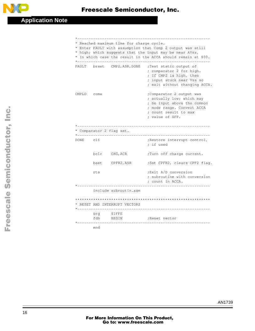
*-----------------------------------------------------------* Reached maximum time for charge cycle.* Enter FAULT with assumption that Comp 2 output was still* high; which suggests that the input may be near AVss.* In which case the result in the ACCA should remain at $00.*-----------------------------------------------------------FAULT brset CMP2,ASR,DONE ;Test static output of
; comparator 2 for high.; If CMP2 is high, then; input stuck near Vss so; exit without changing ACCA.
CMPLO coma ;Comparator 2 output was; actually low; which may; be input above the common; mode range. Convert ACCA; count result to max; value of $FF.
*-----------------------------------------------------------* Comparator 2 flag set.*-----------------------------------------------------------DONE cli ;Restore interrupt control,
; if used
bclr CHG,ACR ;Turn off charge current.
bset CPFR2,ASR ;Set CPFR2, clears CPF2 flag.
rts ;Exit A/D conversion; subroutine with conversion; count in ACCA.
This A/D example is the same as A/D #1 except that in mode 1 the CHG bit is automatically reset when the comparator output sets the CPF2 flag as shown in the flow chart in Figure 4 and the listing in Software Listing 2 — Mode 1 A/D Conversions.
Mode 1 looks identical to the mode 0 example except for the exit method from ATDGO subroutine. But mode 1 has one tricky aspect dealing with the CHG bit. These changes are so minor that the setup subroutine (INIT1) looks very similar to mode 0 (INIT0) with the ACR initialized to $25 instead of $05. This sets the ATD1 bit and switches the A/D mode from 0 to 1. The software timing loop is also unchanged. But, the end of the ATDGO subroutine differs from Software Listing 1 — Mode 0 A/D Conversions with several changes given in the partial listing in Software Listing 2 — Mode 1 A/D Conversions:
1. The clearing of the CHG bit is omitted from the exit of the A/D subroutine in mode 1, since the CHG bit is automatically reset by hardware when the CPF2 bit becomes set.
2. However the clearing of the CHG bit should be added to the FAULT routine for mode 1, since the CHG bit will not be automatically reset if the CPF2 bit never gets set. The clearing of the CHG bit must occur before the test of the CMP2 bit using a BRSET.
Therefore, it appears that the mode 1 functionality does not add any significant value over mode 0. Historically mode 1 was the result of using all of the four states of the mode selection bits, ATD1 and ATD2.
bcc ATDLP ;If accum. count reaches; maximum, then carry will; be set. If carry is clear; then A/D loop count should; continue, else continue on; to process fault, with; carry bit set and ACCA; left equal to $00.
AN1739
19 For More Information On This Product,
Go to: www.freescale.com
Application Note
F
ree
sca
le S
em
ico
nd
uc
tor,
I
Freescale Semiconductor, Inc.n
c..
.
*-----------------------------------------------------------* Reached maximum time for charge cycle.* Enter FAULT with assumption that Comp 2 output was still* high; which suggests that the input may be near AVss.* In which case the result in the ACCA should remain at $00.*-----------------------------------------------------------FAULT bclr CHG,ACR ;Force the discharge of the ; ramp cap since the output ; of the comparator cannot ; trigger an automatic ; discharge.
brset CMP2,ASR,DONE ;Test static output of ; comparator 2 for high. ; If CMP2 is high, then ; input stuck near Vss so ; exit without changing ACCA.
CMPLO coma ;Comparator 2 output was ; actually low; which may ; be input above the common ; mode range. Convert ACCA ; count result to max ; value of $FF.
*-----------------------------------------------------------* Comparator 2 flag set.*-----------------------------------------------------------DONE cli ;Restore interrupt control, ; if used. Discharge turned ; on automatically in Mode 1 ; when comparator 2 output ; went high.
bset CPFR2,ASR ;Set CPFR2, clears CPF2 flag.
rts ;Exit A/D conversion ; subroutine with conversion ; count in ACCA.
In this A/D example, the device is placed in mode 2 and the current source is controlled by the 16-bit timer to charge and discharge the PB0 pin. The TOF flag starts the charge cycle and the discharge is turned on after comparator 2 trips the input capture and causes an ICF flag. The resulting time count for the conversion is stored in the input capture register as an 16-bit number. If the next TOF occurs before the ICF, then the input to the comparator is either at or below VSS. The software will follow the flow chart for the background routine given in Figure 5, the timer interrupt routine in Figure 6, and the listing in Software Listing 3 — Interrupt Driven Mode 2 A/D Conversions.
There are additional features to prevent low level inputs near VSS from causing noisy readings. Also included is a maximum time check in case the input should get too close to VSS or above the common mode range of the comparator.
The A/D cycle time is about 131 ms between TOF conversions for a 0.2 µF capacitor and 4 MHz oscillator. Discharge time is about 0.8 ms. Full scale value of $FFF occurs with an input voltage of about 4.0 volts for a 5 volt supply to VDD.
The software example also makes use of the software flag bit, CIP, contained in a defined FLGS variable. The software example is commented to show the reader what is being performed in each step.
AN1739
21 For More Information On This Product,
Go to: www.freescale.com
Application Note
F
ree
sca
le S
em
ico
nd
uc
tor,
I
Freescale Semiconductor, Inc.n
c..
.
Figure 5. Background Flow Chart for A/D #3, #4, and #7
org $0800************************************************************* SETUP DEVICE*-----------------------------------------------------------BEGIN rsp ;Redundant reset of
; stack pointersei ;Redundant set of
; interrupt mask bit, I
jsr INIT0 ;Initialize analog subsystem;Set up oscillator
************************************************************* SETUP ANALOG AND 16-BIT TIMER*-----------------------------------------------------------
lda #%10100010 ;Set ICIE, TOIE and IEDGsta TCR ;Enable both ICF and TOF
; interrupts; and set; detection edge to rising.
;---------------------------------------------------; IMPORTANT - IEDG bit must be set if ICF is to be; driven by comparator 2.;---------------------------------------------------
jsr RESET ;Restore ramp capacitor to; discharged state and reset; A/D conversion process.
clr TIMMSB ;Clear stored time readingclr TIMLSB ; to $0000
lda #%10000001 ;Select HOLD and MUX1sta AMUX ; to initially connect
************************************************************* BACKGROUND PROGRAM* Loop through the background routine and use the Timer* interrupts to detect, calculate, and control any A/D* conversions.*-----------------------------------------------------------BLOOP sei ;Temporarily disable
; interrupts so that; reading of TIMMSB and; TIMLSB registers will; not be corrupted by an; intervening interrupt.
lda TIMMSB ;Transfer time data tosta ATDMSB ; another set of RAMlda TIMLSB ; registers.sta ATDLSB
cli ;Restore interrupts
nop ;Insert background codenop ; routines here; and thennop ; loop back to start ofnop ; background loop.bra BLOOP
************************************************************* TIMER INTERRUPT ROUTINE* When the I-bit is cleared, any interrupt can seize* control. In this software example only the 16-bit Timer* is defined as an interrupt. This interrupt routine* captures the time data from the Input Capture Register* and transfers it to RAM as TIMMSB, TIMLSB. The* background routine will transfer this time data to* another working variable in RAM as ATDMSB, ATDLSB.** Signals near Vss which may cause extra ICFs later in* the TOF cycle have been reduced by means of the CIP* flag bit which helps to lock out further ICFs until* the next TOF is detected.** Additional feature added to check if TOF is received* while the CIP flag is still set. This indicates that* there was no intervening ICF and the comparator 2 inputs* may be stuck near Vss or above the common mode range.*-----------------------------------------------------------TIMER brset ATD2,ACR,CKICF ;If Mode 2 already established
; check for ICF present, elsebrset TOF,TSR,GOMD2 ; check for TOF present.
RSTMD jsr RESET ;No TOF or Mode 2, thereforebra TEXIT ; ignore and reset analog
; and flags.
AN1739
25 For More Information On This Product,
Go to: www.freescale.com
Application Note
F
ree
sca
le S
em
ico
nd
uc
tor,
I
Freescale Semiconductor, Inc.n
c..
.
GOMD2 jsr SETMD2 ;First TOF, so go set upbra TEXIT ; Mode 2 for first time.
CKICF brset ICF,TSR,CKCPF2 ;If ICF present go checkbra CKTOF ; for valid CPF2 flag, else
; go check for TOF.
CKCPF2 brset CPF2,ASR,CKTOF ;If valid CPF2 flag isbra RSTMD ; present then go check
; for TOF, else reset A/D.
CKTOF brset TOF,TSR,GOTTOF ;Check if TOF present.
brset ICF,TSR,ICF1 ;Check if ICF present.bra RSTMD ;No ICF or TOF, therefore
; reset analog and flags.
ICF1 brset CIP,FLGS,GETTIM ;Test for CIP flag to see if; a conversion was still in; progress. If so, then the; ICF is valid end of a; conversion.
lda ICRL ;Extra ICF found when nobra CLCPF2 ; conversion in progress, so
; clear ICF and ignore.
;---------------------------------------------------; TOF ENCOUNTERED; Always clear the TOF before clearing the ICF. If a ; TOF and ICF are both set, clearing the ICF first ; will cause an immediate start of a new charge; cycle without regard for actual timing of the TOF.;---------------------------------------------------GOTTOF lda TMRL ;Clear TOF
brset ICF,TSR,CKICF2 ;Check if ICF present.
brset CIP,FLGS,STUCK ;Check for CIP flag; showing a conversion; was still in progress.
GOCONV bset CIP,FLGS ;Set CIP to indicatebra TEXIT ; that a conversion has
; been started.
CKICF2 brset CPF2,ASR,ICF2 ;Test for CPF2 flag with; ICF for validity.
bra RSTMD ;No ICF with CPF2, therefore; reset analog and flags.
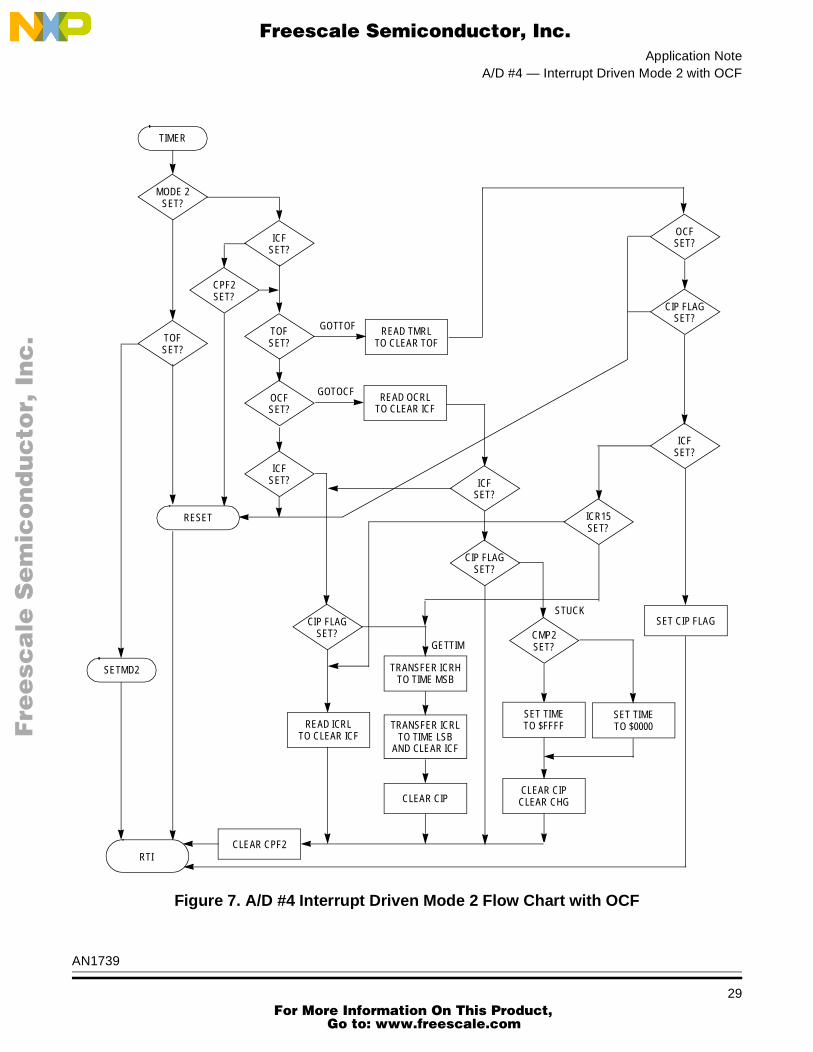
Mode 2 conversions as in A/D #3 can be enhanced to give an earlier detection of a time-out if the OCF in the 16-bit timer is not being used for some other function. This example is the same as A/D #3 except that if an OCF occurs while a conversion is still in progress, then the input to the comparator is either near or below VSS or out of the common mode range. The software will follow the background flow chart given in Figure 5, the timer interrupt flow chart given in Figure 7; and the listing in Software Listing 4 — Interrupt Driven Mode 2 A/D Conversions with OCF.
The software example also makes use of the software flag bit, CIP, contained in a defined FLGS variable. The software example is commented to show the reader what is being performed in each step.
AN1739
28 For More Information On This Product,
Go to: www.freescale.com
Application NoteA/D #4 — Interrupt Driven Mode 2 with OCF
************************************************************* Program Specific Parameter Values*-----------------------------------------------------------OVRFLW equ $C0 ;Count for MSB of OCR to
; check conversion overflow.
org $0800************************************************************* SETUP DEVICE*-----------------------------------------------------------BEGIN rsp ;Redundant reset of
; stack pointer sei ;Redundant set of
; interrupt mask bit, I
jsr INIT0 ;Initialize analog subsystem;Set up oscillator
************************************************************* SETUP ANALOG AND 16-BIT TIMER*----------------------------------------------------------- lda #%11100010 ;Set ICIE, OCIE, TOIE and IEDG sta TCR ;Enable both ICF and TOF
; interrupts; and set; detection edge to rising.
;---------------------------------------------------; IMPORTANT - IEDG bit must be set if ICF is to be; driven by comparator 2.;---------------------------------------------------
lda #OVRFLW ;Update TEMP value withsta TEMP ; new value for OCRjsr RESET ;Restore ramp capacitor to
; discharged state and reset; A/D conversion process.
clr TIMMSB ;Clear stored time reading clr TIMLSB ; to $0000
lda #%10000001 ;Select HOLD and MUX1 sta AMUX ; to initially connect
; PB1 direct to input of; comparator 2.
cli ;Enable all interrupts
************************************************************* BACKGROUND PROGRAM* Loop through the background routine and use the Timer* interrupts to detect, calculate, and control any A/D* conversions.*-----------------------------------------------------------BLOOP sei ;Temporarily disable
; interrupts so that; reading of TIMMSB and; TIMLSB registers will; not be corrupted by an; intervening interrupt.
lda TIMMSB ;Transfer time data to sta ATDMSB ; another set of RAM lda TIMLSB ; registers. sta ATDLSB
cli ;Restore interrupts
nop ;Insert background code nop ; routines here; and then nop ; loop back to start of nop ; background loop. bra BLOOP
************************************************************* TIMER INTERRUPT ROUTINE* When the I-bit is cleared, any interrupt can seize* control. In this software example only the 16-bit Timer* is defined as an interrupt. This interrupt routine* captures the time data from the Input Capture Register* and transfers it to RAM as TIMMSB, TIMLSB. The* background routine will transfer this time data to* another working variable in RAM as ATDMSB, ATDLSB.** Signals near Vss which may cause extra ICFs later in* the TOF cycle have been reduced by means of the CIP* flag bit which helps to lock out further ICFs until* the next TOF is detected.** Additional feature added to check if OCF is received* while the CIP flag is still set. This indicates that* there was no intervening ICF and the comparator 2 inputs* may be stuck near Vss or above the common mode range.*-----------------------------------------------------------
AN1739
31 For More Information On This Product,
Go to: www.freescale.com
Application Note
F
ree
sca
le S
em
ico
nd
uc
tor,
I
Freescale Semiconductor, Inc.n
c..
.
TIMER brset ATD2,ACR,CKICF ;Check if Mode 2 has already; been established.
brset TOF,TSR,GOMD2 ;Check if TOF present.
RSTMD lda #OVRFLW ;Update TEMP value withsta TEMP ; new value for OCRjsr RESET ;No TOF or Mode 2, therefore
bra TEXIT ; ignore and reset analog; and flags.
GOMD2 jsr SETMD2 ;First TOF, so go set up bra TEXIT ; Mode 2 for first time.
CKICF brset ICF,TSR,CKCPF2 ;If ICF present go checkbra CKTOF ; for valid CPF2 flag, else
; go check for TOF.
CKCPF2 brset CPF2,ASR,CKTOF ;If valid CPF2 flag go checkbra RSTMD ; for TOF, else reset A/D.
CKTOF brset TOF,TSR,GOTTOF ;Check if TOF present.
brset OCF,TSR,GOTOCF ;Check if OCF present.
brset ICF,TSR,ICF1 ;Check for ICF present.bra RSTMD ;No interrupt flags so
; reset A/D.
ICF1 brset CIP,FLGS,GETTIM ;Test for CIP flag to see if; a conversion was still in; progress. If so, then the; ICF is valid end of a; conversion.
CLRICF lda ICRL ;Extra ICF found when no bra CLCPF2 ; conversion in progress, so ; clear ICF and ignore.
;---------------------------------------------------; TOF ENCOUNTERED; Always clear the TOF before clearing the ICF. If a ; TOF and ICF are both set, clearing the ICF first ; will cause an immediate start of a new charge; cycle without regard for actual timing of the TOF.;---------------------------------------------------GOTTOF lda TMRL ;Clear TOF
brset OCF,TSR,RSTMD ;If OCF also present reset; A/D, else go check for ; CIP flag.
brset CIP,FLGS,RSTMD ;If CIP also present reset; A/D, else go check for; an ICF.
************************************************************* RESET AND INTERRUPT VECTORS*-----------------------------------------------------------
org $1FF6fdb TIMER ;Timer vectororg $1FFEfdb BEGIN ;Reset vector
*----------------------------------------------------------- end
A/D #5 — Non-Interrupt Driven Mode 2
In this A/D example the device is placed in mode 2 with similar performance to A/D #3, except that this example does not rely on enabling the timer interrupts and requires additional checks to make sure that the TOF and ICF are in the proper sequence. The software will follow the flow chart given in Figure 8 and the listing in Software Listing 5 — Non-Interrupt Driven Mode 2 A/D Conversions.
The software example does not make use of the software flag bit, CIP. The software example is commented to show the reader what is being performed in each step.
************************************************************* Program Specific Parameter Values*-----------------------------------------------------------LIMIT equ $C0 ;Limit for time MSB
org $0800************************************************************* SETUP DEVICE*-----------------------------------------------------------BEGIN rsp ;Redundant reset of
; stack pointersei ;Redundant set of
; interrupt mask bit, I
jsr INIT0 ;Initialize analog subsystem;Set up oscillator
************************************************************* SETUP ANALOG AND 16-BIT TIMER*-----------------------------------------------------------
lda #%00000010 ;Set IEDG for detectionsta TCR ; of rising edge to ICF.
;---------------------------------------------------; IMPORTANT - IEDG bit must be set if ICF is to be; driven by comparator 2.;---------------------------------------------------
jsr RESET ;Restore ramp capacitor to; discharged state and reset; A/D conversion process.
clr ATDMSB ;Clear stored time readingclr ATDLSB ; to $0000
lda #%10000001 ;Select HOLD and MUX1sta AMUX ; to initially connect
************************************************************* BACKGROUND PROGRAM* Loop through the background routine and use the Timer* interrupt flags to detect, calculate, and control any A/D* conversions.*-----------------------------------------------------------BLOOP brset TOF,TSR,CHKMD ;If TOF found go check for
bra LOOP ; Mode 2, else skip checks
CHKMD brset ATD2,ACR,CKICF ;If Mode 2 already establishedjsr SETMD2 ; check for ICF present, elsebra LOOP ; set up Mode 2.
CKICF brset ICF,TSR,GOTICF ;If ICF present go get; conversion data, else; go check for overrun.
CHKTM lda ACRH ;Fetch MSB of timer count.cmp #LIMIT ;Check against max limit.bhs MAXTM ;If over limit go checkbra LOOP ; comparator state, else
; continue with background.
GOTICF lda ICRH ;Check MSB of ICF datacmp #LIMIT ; against limit.bhs SETMAX ; If higher or same set thesta ATDMSB ; A/D result to $FFFF, elselda ICRL ; transfer ICR contents tosta ATDLSB ; to A/D result.bra RSTATD
MAXTM brset CMP2,ASR,SETLO ;If CMP2 set then comparator; input stuck low, else it; is stuck high.
SETMAX lda #$FF ;Default A/D result to thesta ATDMSB ; maximum value of $FFFF.sta ATDLSBbra RSTATD
SETLO lda #$00 ;Default A/D result to thesta ATDMSB ; minimum value of $0000.sta ATDLSB
RSTATD lda TSR ;Read the TSR to arm flags; for clearing.
;---------------------------------------------------; IMPORTANT - Always clear TOF before clearing ICF.;---------------------------------------------------
lda TMRL ;Clear TOF flag, if any.lda ICRL ;Clear ICF flag, if any.bset CPFR2,ASR ;Clear CPF2 flag, if any.
AN1739
37 For More Information On This Product,
Go to: www.freescale.com
Application Note
F
ree
sca
le S
em
ico
nd
uc
tor,
I
Freescale Semiconductor, Inc.n
c..
.
bclr CHG,ACR ;Force discharge of PB0; for case where time; was over limit.
CALC lda ATDMSB ;Transfer A/D result to thesta TIMMSB ; other background routines.lda ATDLSBsta TIMLSB
The mode 2 conversions in A/D #5 can be enhanced to give an earlier detection of a time-out if the OCF in the 16-bit timer is not being used for some other function. This A/D example is the same as A/D #5 except that this example does not rely on enabling the timer interrupts and requires additional checks to make sure that the TOF, OCF, and ICF are in the proper sequence. The software will follow the flow chart given in Figure 9 and the listing in Software Listing 6 — Non-Interrupt Driven Mode 2 A/D Conversions with OCF.
The software example does not make use of the software flag bit, CIP. The software example is commented to show the reader what is being performed in each step.
AN1739
38 For More Information On This Product,
Go to: www.freescale.com
Application NoteA/D #6 — Non-Interrupt Driven Mode 2 with OCF
************************************************************* Program Specific Parameter Values*-----------------------------------------------------------LIMIT equ $10 ; Limit for time using OCF MSB
org $0800************************************************************* SETUP DEVICE*-----------------------------------------------------------BEGIN rsp ;Redundant reset of
; stack pointersei ;Redundant set of
; interrupt mask bit, I
jsr INIT0 ;Initialize analog subsystem;Set up oscillator
************************************************************* SETUP ANALOG AND 16-BIT TIMER*-----------------------------------------------------------
lda #%00000010 ;Set IEDG for detectionsta TCR ; of rising edge to ICF.
;---------------------------------------------------; IMPORTANT - IEDG bit must be set if ICF is to be; driven by comparator 2.;---------------------------------------------------
lda #LIMIT ;Update TEMP value withsta TEMP ; new value for OCRjsr RESET ;Restore ramp capacitor to
; discharged state and reset; A/D conversion process.
clr ATDMSB ;Clear stored time readingclr ATDLSB ; to $0000
lda #%10000001 ;Select HOLD and MUX1sta AMUX ; to initially connect
************************************************************* BACKGROUND PROGRAM* Loop through the background routine and use the Timer* interrupt flags to detect, calculate, and control any A/D* conversions.*-----------------------------------------------------------BLOOP brset OCF,TSR,CKTOF ;If OCF found go check for
brset TOF,TSR,CHKMD ;If TOF found go check forbra LOOP ; Mode 2, else skip checks.
CKTOF brset TOF,TSR,CHKMD ;If TOF also present thenlda OCRL ; OCF is valid overrun of time,bra LOOP ; else reset OCF.
CHKMD brset ATD2,ACR,CKICF ;If Mode 2 already establishedjsr SETMD2 ; check for ICF present, elsebra LOOP ; set up Mode 2.
CKICF brset ICF,TSR,GOTICF ;If ICF present go get; conversion data, else; go check for overrun.
brset OCF,TSR,MAXTM ;Check for OCF to see ifbra LOOP ; over time limit, else
; continue with loop.
GOTICF brset OCF,TSR,SETMAX ;If OCF found then max out; the A/D result
lda ICRH ;Transfer ICF data to thesta ATDMSB ; A/D result registers.lda ICRLsta ATDLSBbra RSTATD
MAXTM brset CMP2,ASR,SETLO ;If CMP2 set then comparator; input stuck low, else it; is stuck high.
SETMAX lda #$FF ;Default A/D result to thesta ATDMSB ; maximum value of $FFFF.sta ATDLSBbra RSTATD
SETLO lda #$00 ;Default A/D result to thesta ATDMSB ; minimum value of $0000.sta ATDLSB
RSTATD lda TSR ;Read the TSR to arm flags; for clearing.
AN1739
41 For More Information On This Product,
Go to: www.freescale.com
Application Note
F
ree
sca
le S
em
ico
nd
uc
tor,
I
Freescale Semiconductor, Inc.n
c..
.
;---------------------------------------------------; IMPORTANT - Always clear TOF and OCF before; clearing ICF.;---------------------------------------------------
lda TMRL ;Clear TOF flag, if any.lda OCRL ;Clear OCF flag, if any.lda ICRL ;Clear ICF flag, if any.bset CPFR2,ASR ;Clear CPF2 flag, if any.bclr CHG,ACR ;Force discharge of PB0.
CALC lda ATDMSB ;Transfer A/D result to thesta TIMMSBlda ATDLSBsta TIMLSB
In this A/D example the device is placed in mode 3 and the current source is controlled by the 16-bit timer to charge and discharge the PB0 pin. The OCF flag starts the charge cycle and the discharge is turned on after comparator 2 trips the input capture and causes an ICF flag. The resulting time count for the conversion is stored in the input capture register as an 16-bit number. If the next OCF occurs before the ICF, then the input to the comparator is either at or below VSS.
There are additional features to prevent low level inputs near VSS from causing noisy readings. Also included is a maximum time check in case the input should get too close to VSS or above the common mode range of the comparator.
The A/D cycle time is about 16 ms between OCF conversions for a 0.2 µF capacitor and 4 MHz oscillator. Discharge time is about 0.8 ms. Full scale value of $FFF occurs with an input voltage of about 4.0 volts for a 5 volt supply to VDD. The software will follow the background flow chart given in Figure 5, the timer interrupt flow chart given in Figure 10, and the listing in Software Listing 7 — Interrupt Driven Mode 3 A/D Conversions.
The software example also makes use of the software flag bit, CIP, contained in a defined FLGS variable. The software example is commented to show the reader what is being performed in each step.
************************************************************* Program Specific Parameter Values*-----------------------------------------------------------STEP equ $20 ;Step for MSB of OCRDSTEP equ $40 ;Double step for MSB of OCRMAXMSB equ $1F ;Set limit for MSB of time
org $0800************************************************************* SETUP DEVICE*-----------------------------------------------------------BEGIN rsp ;Redundant reset of
; stack pointersei ;Redundant set of
; interrupt mask bit, I
jsr INIT0 ;Initialize analog subsystem;Set up oscillator
************************************************************* SETUP ANALOG AND 16-BIT TIMER*-----------------------------------------------------------
lda #%11000010 ;Set ICIE, OCIE and IEDGsta TCR ;Enable both ICF and OCF
; interrupts; and set; detection edge to rising.
;---------------------------------------------------; IMPORTANT - IEDG bit must be set if ICF is to be; driven by comparator 2.;---------------------------------------------------
lda OCRH ;Fetch current OCR MSBadd #DSTEP ;Update to twice normalsta TEMP ; stepjsr RESET ;Restore ramp capacitor to
; discharged state and reset; A/D conversion process.
clr TIMMSB ;Clear stored time readingclr TIMLSB ; to $0000
AN1739
45 For More Information On This Product,
Go to: www.freescale.com
Application Note
F
ree
sca
le S
em
ico
nd
uc
tor,
I
Freescale Semiconductor, Inc.n
c..
.
lda #%10000001 ;Select HOLD and MUX1sta AMUX ; to initially connect
; PB1 direct to input of; comparator 2.
cli ;Enable all interrupts
************************************************************* BACKGROUND PROGRAM* Loop through the background routine and use the Timer* interrupts to detect, calculate, and control any A/D* conversions.*-----------------------------------------------------------BLOOP sei ;Temporarily disable
; interrupts so that; reading of TIMMSB and; TIMLSB registers will; not be corrupted by an; intervening interrupt.
lda TIMMSB ;Transfer time data tosta ATDMSB ; another set of RAMlda TIMLSB ; registers.sta ATDLSB
cli ;Restore interrupts
nop ;Insert background codenop ; routines here; and thennop ; loop back to start ofnop ; background loop.bra BLOOP
************************************************************* TIMER INTERRUPT ROUTINE* When the I-bit is cleared, any interrupt can seize* control. In this software example only the 16-bit Timer* is defined as an interrupt. This interrupt routine* captures the time data from the Input Capture Register* and transfers it to RAM as TIMMSB, TIMLSB. The* background routine will transfer this time data to* another working variable in RAM as ATDMSB, ATDLSB.** The next OCF needs to be calculated each time an OCF* is detected. The time measurement is the ICR data* minus the "start" time for the OCF that started the* conversion cycle.** Signals near Vss which may cause extra ICFs later in* the OCF cycle have been reduced by means of the CIP* flag bit which helps to lock out further ICFs until* the next OCF is detected.*
* Additional feature added to check if TOF is received* while the CIP flag is still set. This indicates that* there was no intervening ICF and the comparator 2 inputs* may be stuck near Vss or above the common mode range.*-----------------------------------------------------------TIMER lda ACR ;Fetch contents of ACR
and #%01100000 ;Mask off ATD1 and ATD2 bits.cmp #%01100000 ;Check if Mode 3 has alreadybeq CKICF ; been established.
brset OCF,TSR,GOMD3 ;Check if OCF present.
RSTMD lda OCRH ;Fetch current OCR MSBadd #DSTEP ;Update to twice normalsta TEMP ; stepjsr RESET ;No OCF or Mode 3, thereforejmp TEXIT ; ignore and reset analog
; and flags.
GOMD3 lda OCRH ;Fetch current OCR MSBadd #DSTEP ;Update to twice normalsta TEMP ; stepjsr SETMD3 ;First OCF, so go set upbra TEXIT ; Mode 3 for first time.
CKICF brset ICF,TSR,CKCPF2 ;If ICF set go check forbra CKOCF ; valid CPF2, else go
; check for an OCF.
CKCPF2 brset CPF2,ASR,CKOCF ;If valid CPF2 go checkbra RSTMD ; for OCF, else reset A/D.
CKOCF brset OCF,TSR,GOTOCF ;Check if OCF present.
brset ICF,TSR,ICF1 ;Check if ICF present.bra RSTMD ;No ICF or TOF, therefore
; reset analog and flags.
ICF1 brset CIP,FLGS,GETTIM ;Test for CIP flag to see if; a conversion was still in; progress. If so, then the; ICF is valid end of a; conversion.
lda ICRL ;Extra ICF found when nobra CLCPF2 ; conversion in progress, so
; clear ICF and ignore.
;---------------------------------------------------; OCF ENCOUNTERED ; Always clear the OCF before clearing the ICF. If; an OCF and ICF are both set, clearing the ICF; first will cause an immediate start of a new; charge cycle without regard for the actual timing ; of the OCF.;---------------------------------------------------
AN1739
47 For More Information On This Product,
Go to: www.freescale.com
Application Note
F
ree
sca
le S
em
ico
nd
uc
tor,
I
Freescale Semiconductor, Inc.n
c..
.
GOTOCF lda OCRH ;Fetch MSB of OCR.sta STMMSB ;Update MSB of start time.add #STEP ;Add MSB of step.sta OCRH ;Update MSB of OCR.clr OCRL ;Clear LSB of OCR and clear
; OCF, if any.clr STMLSB ;Update LSB of start time.
brset ICF,TSR,ICF2 ;Check if ICF present.
brset CIP,FLGS,STUCK ;Check for CIP flag; showing a conversion; was still in progress.
GOCONV bset CIP,FLGS ;Set CIP to indicatebra TEXIT ; that a conversion has
; been started.
ICF2 brset CIP,FLGS,CLRICF ;Check for CIP flag; showing that conversion; is in progress.
ldx ICRH ;Fetch MSB of ICR.lda ICRL ;Fetch LSB of ICR, and clear
; any ICF present.clc ;Clear any borrow pending.sub STMLSB ;Subtract LSB of start time.txa ;Move MSB of ICR to accumulator.
; Borrow not affected by this; operation.
sbc STMMSB ;Subtract MSB of start time; and any borrow from MSB of; captured ICR.
bcs IGNORE ; result of calculated time.bra GETTIM
CLRICF lda ICRL ;ICF captured near next; OCF, so ignore ICF and; check CMP2.
STUCK brset CMP2,ASR,STKLOW ;Check output of comparator; 2 to determine input; state.
bclr CHG,ACR ;Clear CHG bit in ACRbra CLCPF2 ; to discharge ramp
; capacitor due to; infinite conversion.; (OCF was already cleared; above at GOTOCF.)
STKLOW clr TIMMSB ;Comparator 2 output wasclr TIMLSB ; high, therefore input wasbra CLRCHG ; near Vss or lower.
IGNORE lda ICRL ;Read ICRL to clear ICF.bra CLRCHG ;GO clear CHG bit in ACR.
;---------------------------------------------------; Check to see if conversion time getting too close; to next OCF such that the ramp capacitor cannot; discharge in time.;---------------------------------------------------GETTIM ldx ICRH ;Fetch MSB of ICR.
lda ICRL ;Fetch LSB of ICR, and clear; any ICF present.
clc ;Clear any borrow pending.sub STMLSB ;Subtract LSB of start time.sta TIMLSB ;Save LSB of calculated time.txa ;Move MSB of ICR to accumulator.
; Borrow not affected by this; operation.
sbc STMMSB ;Subtract MSB of start time; and any borrow from MSB of; captured ICR.
sta TIMMSB ;Save MSB of calculated time.
lda TIMMSB ;Fetch MSB of time.cmp #MAXMSB ;Check against limit.blo CLRCIP ;If MSB less than limitjmp RSTMD ; then OK, else reset A/D.
CLRCIP bclr CIP,FLGS ;Clear CIP to indicate; that conversion is over.
In this A/D example the device is placed in mode 3 similar to A/D #7 except that this example does not rely on enabling the timer interrupts and requires additional checks to make sure that the OCF and ICF are in the proper sequence. The software will follow the flow chart given in Figure 11 and the listing in Software Listing 8 — Non-Interrupt Driven Mode 3 A/D Conversions.
The software example does not make use of the software flag bit, CIP. The software example is commented to show the reader what is being performed in each step.
************************************************************* Program Specific Parameter Values*-----------------------------------------------------------STPMSB equ $20 ;MSB of time step for next OCFSTPLSB equ $00 ;LSB of time step for next OCFLMTMSB equ $18 ;MSB of time limit from last OCFLMTLSB equ $00 ;LSB of time limit from last OCF
org $0800************************************************************* SETUP DEVICE*-----------------------------------------------------------BEGIN rsp ;Redundant reset of
; stack pointersei ;Redundant set of
; interrupt mask bit, I
jsr INIT0 ;Initialize analog subsystem;Set up oscillator
************************************************************* SETUP ANALOG AND 16-BIT TIMER*-----------------------------------------------------------
lda #%00000010 ;Set IEDG for detectionsta TCR ; of rising edge to ICF.
;---------------------------------------------------; IMPORTANT - IEDG bit must be set if ICF is to be; driven by comparator 2.;---------------------------------------------------
lda TMRH ;Fetch MSB of current timeadd #STPMSB ;Calculate next OCR timesta TEMPjsr RESET ;Restore ramp capacitor to
; discharged state and reset; A/D conversion process.
clr ATDMSB ;Clear stored time readingclr ATDLSB ; to $0000
lda #%10000001 ;Select HOLD and MUX1sta AMUX ; to initially connect
************************************************************* BACKGROUND PROGRAM* Loop through the background routine and use the Timer* interrupt flags to detect, calculate, and control any A/D* conversions.*-----------------------------------------------------------BLOOP brset OCF,TSR,CHKMD ;If OCF found go check for
bra LOOP ; Mode 3, else skip checks.
CHKMD brset ATD2,ACR,CKICF ;If Mode 3 already established; ignore state of ATD1 bit
lda TMRH ;Fetch MSB of current timeadd #STPMSB ;Calculate next OCR timesta TEMPjsr SETMD3 ; check for ICF present, elsebra LOOP ; set up Mode 3.
CKICF brset ICF,TSR,GOTICF ;If ICF present go get; conversion data, else; go check for overrun.
CKTIM clc ;Clear any borrow pending.
ldx ACRH ;Fetch MSB of ACR.lda ACRL ;Fetch LSB of ACR
sub STMLSB ;Subtract LSB of start time.sta DIFLSB
txa ;Move MSB of time to accumulator.; Borrow not affected by this; operation.
sbc STMMSB ;Subtract MSB of start timesta DIFMSB ; and any borrow from MSB of
; present time.
bcs LOOP ;If carry set the time was; before the OCF and ignore.
jsr CHKLMT ;Check if time over limit.bcs MAXTM ;If over time limit go testbra LOOP ; for reason, else continue
; with loop.
GOTICF clc ;Clear any borrow pending.
ldx ICRH ;Fetch MSB of ICR.lda ICRL ;Fetch LSB of ICR, and clear
; any ICF present.
sub STMLSB ;Subtract LSB of start time.sta DIFLSB ;Save LSB of calculated time.
txa ;Move MSB of ICR to accumulator.; Borrow not affected by this; operation.
AN1739
53 For More Information On This Product,
Go to: www.freescale.com
Application Note
F
ree
sca
le S
em
ico
nd
uc
tor,
I
Freescale Semiconductor, Inc.n
c..
.
sbc STMMSB ;Subtract MSB of start time; and any borrow from MSB of; captured ICR.
sta DIFMSB ;Save MSB of calculated time.
bcs IGNORE ;If borrow set then ICF occurred; before the OCF. Ignore ICF and; OCF cycle.
jsr CHKLMT ;Check if time over limit.bcs MAXTM ;If over time limit go set
; result to max value, else; go clear flags.
lda DIFMSB ;Transfer valid time differencesta ATDMSB ; to A/D result registerslda DIFLSBsta ATDLSBbra RSTATD
IGNORE bset CPFR2,ASR ;Clear CPF2 flag.bra LOOP
MAXTM brset CMP2,ASR,SETLO ;If CMP2 set then comparator; input stuck low, else it; is stuck high.
SETMAX lda #$FF ;Default A/D result to thesta ATDMSB ; maximum value of $FFFF.sta ATDLSBbra RSTATD
SETLO lda #$00 ;Default A/D result to thesta ATDMSB ; minimum value of $0000.sta ATDLSB
RSTATD lda STMLSB ;Fetch LSB of start time.add #STPLSB ;Add LSB of time step.
sta STMLSB ;Save as new start time.tax ;Save LSB in index register.
lda STMMSB ;Fetch MSB of start time.adc #STPMSB ;Add MSB of time step plussta STMMSB ; any carry.
sta OCRH ;Update OCRH, hold compare
;---------------------------------------------------; IMPORTANT - Always clear TOF and OCF before; clearing ICF.;---------------------------------------------------
************************************************************* LOCAL PROGRAM SUBROUTINES************************************************************* CHKLMT, Check Time Limit Subroutine* This routine calculates the time limit minus the* difference from the previous calculation.If the* number is negative (borrow set) then the difference* time exceeded the limit.*-----------------------------------------------------------CHKLMT clc ;Clear any borrow pending.
lda LMTLSB ;Fetch LSB of time limit.
sub DIFLSB ;Subtract LSB of difference.
lda LMTMSB ;Fetch MSB of time limit.sbc DIFMSB ;Subtract MSB of difference.
rts ;Return with borrow set for; time over limit or borrow; clear for time OK.
************************************************************* RESET AND INTERRUPT VECTORS*-----------------------------------------------------------
There are a number of design considerations in using channel selection, sample and hold, and other A/D related topics. The design checks which should be observed when using the JJ/JP series MCUs for single slope A/D conversion are given briefly in Table A-1. Further information can be found in Applications Using the Analog Subsystem on MC68HC05JJ/JP Series Microcontrollers, Freescale document order number AN1740/D.
7DEOH�$����$�'�&RQYHUVLRQ�'HVLJQ�&KHFNV
Function Design Check
A/DBe sure to calculate the common mode range over the range of voltage levels expected for
VDD; and always keep one input to the voltage comparators within the common mode range.
A/DIt is important that the INV and VOFF bits are not changed during the time that a voltage is
being held on the sample capacitor.
A/DWhen calculating the minimum and maximum values for CEXT, VFS, ICHG, and fOSC be sure to
include any effects caused by expected changes in supply voltage and temperature.
Channel Multiplexers
The simple channel multiplexers do not include any automatic break-before-make or make-before-break control of multiple simultaneous changes. Therefore, the user must control the multiplexers in the proper sequence to avoid shorting two channels together during the transition.
ComparatorsBefore sampling the comparator outputs or clearing the CPF1 or CPF2 flags be sure to allow
sufficient delay after the comparators are powered up. Otherwise, the outputs may be undefined or the flags may not be cleared.
ComparatorsThe CPF2 flag bit may get set incorrectly when changing channels to an input source voltage
which is near VSS. A/D conversion software should account for this case and clear out any unwanted CPF2 flags before starting another conversion.
ComparatorWhen operating with one comparator input near VSS it is recommended that the input always be
tested with the INV bit both set and clear. If the results are different, then the inputs are both within VIO of VSS.
ComparatorChanges to the INV, CP1EN, CP2EN, and ICEN bits can cause the comparator static flags to
get set. Always clear the CPF1 and CPF2 static flag bits after changing any configuration of the comparators.
Discharge Device
Discharging large capacitors or low impedance loads into the PB0 pin can cause high current spikes which may disrupt the internal analog VSS and cause unwanted analog noise.
EPROMThe window on erasable EPROM devices must be covered with an opaque material such as
black electrical tape. Common white paper labels are not opaque enough to prevent light from affecting bias currents, trip points, and leakage in the analog subsystem.
Input DividerThe divided input is only compensated for one channel multiplexer at a time. If multiple channel
multiplexers are on simultaneously, then the divider ratio will increase slightly.
InterruptsAvoid using BOTH the input capture and the analog interrupt at the same time for the
comparator trip detection. The ICF always wins priority and the analog interrupt will essentially be ignored.
PulldownsBe sure to turn off the pulldown on the PB0 pin when used for A/D conversions. Leaving this
pulldown on can lead to a nonlinear charge waveform and unexpected measurement results.
PulldownsThe most common cause of unwanted input current or low input impedance is a failure to turn
off the input pulldown devices.
Sample & Hold
The sample capacitor can typically hold its charge for several minutes at room temperature, but due to inherent leakage currents this degrades quickly as the temperature is raised.
Sample & Hold
Experience has shown that the least sensitivity to noise sources is created when the channel select bus is connected to the internal VDD after the HOLD of DHOLD multiplexer has been turned off.
Sample & Hold
In cases where severe system noise affects input signal measurements it is recommended that the sample and hold method not be used.
Sample & Hold
When trying to maintain the sample voltage avoid discharging capacitors or other high current loads through the MCU’s VSS pin or power supply return wiring.
Sample & Hold
When using the sample and hold capacitor, always turn off the HOLD and DHOLD bits on a separate write to the AMUX register before making any changes to the other channel multiplexers.
16-Bit TimerAlways clear the TOF and OCF before clearing the ICF. Otherwise, clearing the ICF will
immediately enable any existing TOF or OCF to control charging of the PB0 pin without regard for their proper timing points.
16-Bit TimerAvoid clearing the CPF2 comparator static flag too quickly after clearing the ICF as this enables
the timer to capture a new time should the comparator output then rise again later.
16-Bit TimerAvoid changing the state of the INV bit after clearing the ICF as this will cause a switching pulse
to set the CPF2 bit and trigger an unwanted ICF.
16-Bit TimerChanges to the ICEN, ICIE, or IEDG bits can cause the ICF flag bit to become set. Always
clear the ICF flag following any change in the state of the ICEN, ICIE, and IEDG bits.
************************************************************* INIT0, Initialize Analog Subsystem to Mode 0 or Mode 1* Discharge sample cap and prepare analog.*-----------------------------------------------------------INIT0 lda #%00000101 ;Set Mode 0
sta ACR ; Turn on comparator 2 and; current source with the; discharge device on.
bra SETMUX
INIT1 lda #%00100101 ;Set Mode 1sta ACR ; Turn on comparator 2 and
; current source with the; discharge device on.
SETMUX lda #%10000000 ;Select HOLD and AVSSsta AMUX ;Connect channel bus and
; sample cap to AVss to; discharge any leftover; charge.
************************************************************* SETOSC, Set Up Oscillator* The oscillator changeover delay allows time to discharge * external capacitor in case a reset was too short for * fully charged capacitor. The initial time delay is based * on the LPO frequency of 500 kHz.*-----------------------------------------------------------SETOSC lda #%01100000 ;Select OM2 and OM1 and
sta ISCR ; write to ISCR.;This turns on both the; LPO and EPO.
ldx #$51 ;Wait for EPO to stabilize.jsr TDELAY ; 2.0 msec at fosc = 500 kHz.
lda #%00100000 ;Select OM1 only andsta ISCR ; write to ISCR.
;This switches the clock; source to the EPO.
lda #$FF ;Inhibit port B pulldownssta PDRB ; by writing $FF to PDRB.
clr DDRB ;Set up port B as inputs; by clearing the DDRB.
lda #%00110000 ;CPFR2 and CPFR1sta ASR ;Clear any comparatorrts ; flags, if set
************************************************************* RESET, Restore Mode 2 or 3 Subroutine* This routine restores the initial conditions of the analog* subsystem and insures that the ramp capacitor on PB0 is* fully discharged following any reset event. Also includes * initialization routine for establishing Mode 2 or 3 for the * first conversion cycle at entry points SETMD2 or SETMD3.* Value to update OCR with must be in TEMP before call.*-----------------------------------------------------------RESET lda #%00000001 ;Set to Mode 0, reset CHG
bra SETMD ; bit and set ISEN to enable; the discharge device; connected to PB0 to fully; discharge the external; ramp capacitor.
SETMD2 lda #%01010101 ;Set to Mode 2, reset CHGbra SETMD ; bit and enable analog
; by setting ICEN, CP2EN,; and ISEN. Set ATD2 and; clear ATD1.
SETMD3 lda #%01110101 ;Set to Mode 3, reset CHG; bit and enable analog; by setting ICEN, CP2EN,; and ISEN. Set ATD1 and; ATD2.
SETMD sta ACRnop ;Wait 5 microsec (at 2 MHznop ; bus clock) for comparatorsnop ; to stabilize before clearingnop ; any flags.noplda TSR ;Read the TSR to arm flags
; for clearing.
;---------------------------------------------------; IMPORTANT - Always clear OCF before clearing ICF.;---------------------------------------------------
lda TMRL ;Clear TOF flag, if any.
lda TEMP ;Fetch MSB for OCR.sta STMMSB ;Update MSB of start time.sta OCRH ;Update OCRH and lock out
; compare until OCRL is; written.
AN1739
61 For More Information On This Product,
Go to: www.freescale.com
Application Note
F
ree
sca
le S
em
ico
nd
uc
tor,
I
Freescale Semiconductor, Inc.n
c..
.
clr STMLSB ;Clear LSB of start time.clr OCRL ;Clear OCRL and clear OCF,
; if any.
lda ICRL ;Clear ICF flag, if any.
clr FLGS ;Clear CIP flag, if used.
bset CPFR2,ASR ;Clear CPF2 flag, if any.rts
************************************************************* TDELAY, General Purpose Time Delay Subroutine.* Preload and decrement X-register to 0. A complete* setup of X-register, subroutine call and return with a* count of (1) in X-register uses 20 bus cycles. Each* additional count stored to the X-register causes an* additional 6 cycle delay. This is equivalent to:** ( 3 * N + 7) usec at 4 MHz fosc (2 MHz bus)* ( 6 * N + 14) usec at 2 MHz fosc (1 MHz bus)* ( 12 * N + 28) usec at 1 MHz fosc (500 kHz bus)* ( 24 * N + 56) usec at 500 kHz fosc (250 kHz bus)* (120 * N + 280) usec at 100 kHz fosc ( 50 kHz bus)** where (N) equals the count stored to the X-register* before entry.** NOTE: Entering with the X-register set to $00 causes* the longest delay of 1550 bus cycles.*-----------------------------------------------------------TDELAY decx
bne TDELAY ;Loop until X is zero againrts ;Return from subroutine