+ All Categories
Home > Documents > Sensors sensors - MDPI · Sensors 2007, 7 762 investigate the dynamic characteristics of the...

Sensors sensors - MDPI · Sensors 2007, 7 762 investigate the dynamic characteristics of the...

Date post: 30-Apr-2020
Category:
Upload: others
View: 14 times
Download: 0 times
Share this document with a friend
37
Sensors 2007, 7, 760-796 sensors ISSN 1424-8220 © 2007 by MDPI www.mdpi.org/sensors Review Stability, Nonlinearity and Reliability of Electrostatically Actuated MEMS Devices Wen-Ming Zhang 1, *, Guang Meng 1 and Di Chen 2 1 State Key Laboratory of Mechanical System and Vibration, Shanghai Jiao Tong University, 800 Dongchuan Road, Shanghai 200240, China 2 National Key Laboratory of Micro/Nano Fabrication Technology, Shanghai Jiao Tong University, 1954 Huashan Road, Shanghai 200030, China * Author to whom correspondence should be addressed; E-mail: [email protected]. Received: 13 April 2007 / Accepted: 22 May 2007 / Published: 31 May 2007 Abstract: Electrostatic micro-electro-mechanical system (MEMS) is a special branch with a wide range of applications in sensing and actuating devices in MEMS. This paper provides a survey and analysis of the electrostatic force of importance in MEMS, its physical model, scaling effect, stability, nonlinearity and reliability in detail. It is necessary to understand the effects of electrostatic forces in MEMS and then many phenomena of practical importance, such as pull-in instability and the effects of effective stiffness, dielectric charging, stress gradient, temperature on the pull-in voltage, nonlinear dynamic effects and reliability due to electrostatic forces occurred in MEMS can be explained scientifically, and consequently the great potential of MEMS technology could be explored effectively and utilized optimally. A simplified parallel-plate capacitor model is proposed to investigate the resonance response, inherent nonlinearity, stiffness softened effect and coupled nonlinear effect of the typical electrostatically actuated MEMS devices. Many failure modes and mechanisms and various methods and techniques, including materials selection, reasonable design and extending the controllable travel range used to analyze and reduce the failures are discussed in the electrostatically actuated MEMS devices. Numerical simulations and discussions indicate that the effects of instability, nonlinear characteristics and reliability subjected to electrostatic forces cannot be ignored and are in need of further investigation. Keywords: MEMS, Electrostatic force, Scaling effect, Stability, Nonlinearity, Reliability.
Transcript

Sensors 2007, 7, 760-796

sensors ISSN 1424-8220 © 2007 by MDPI

www.mdpi.org/sensors Review

Stability, Nonlinearity and Reliability of Electrostatically Actuated MEMS Devices

Wen-Ming Zhang 1,*, Guang Meng 1 and Di Chen 2 1 State Key Laboratory of Mechanical System and Vibration, Shanghai Jiao Tong University,

800 Dongchuan Road, Shanghai 200240, China 2 National Key Laboratory of Micro/Nano Fabrication Technology, Shanghai Jiao Tong University,

1954 Huashan Road, Shanghai 200030, China

* Author to whom correspondence should be addressed; E-mail: [email protected].

Received: 13 April 2007 / Accepted: 22 May 2007 / Published: 31 May 2007

Abstract: Electrostatic micro-electro-mechanical system (MEMS) is a special branch with

a wide range of applications in sensing and actuating devices in MEMS. This paper

provides a survey and analysis of the electrostatic force of importance in MEMS, its

physical model, scaling effect, stability, nonlinearity and reliability in detail. It is necessary

to understand the effects of electrostatic forces in MEMS and then many phenomena of

practical importance, such as pull-in instability and the effects of effective stiffness,

dielectric charging, stress gradient, temperature on the pull-in voltage, nonlinear dynamic

effects and reliability due to electrostatic forces occurred in MEMS can be explained

scientifically, and consequently the great potential of MEMS technology could be explored

effectively and utilized optimally. A simplified parallel-plate capacitor model is proposed

to investigate the resonance response, inherent nonlinearity, stiffness softened effect and

coupled nonlinear effect of the typical electrostatically actuated MEMS devices. Many

failure modes and mechanisms and various methods and techniques, including materials

selection, reasonable design and extending the controllable travel range used to analyze and

reduce the failures are discussed in the electrostatically actuated MEMS devices.

Numerical simulations and discussions indicate that the effects of instability, nonlinear

characteristics and reliability subjected to electrostatic forces cannot be ignored and are in

need of further investigation.

Keywords: MEMS, Electrostatic force, Scaling effect, Stability, Nonlinearity, Reliability.

Sensors 2007, 7

761

1. Introduction

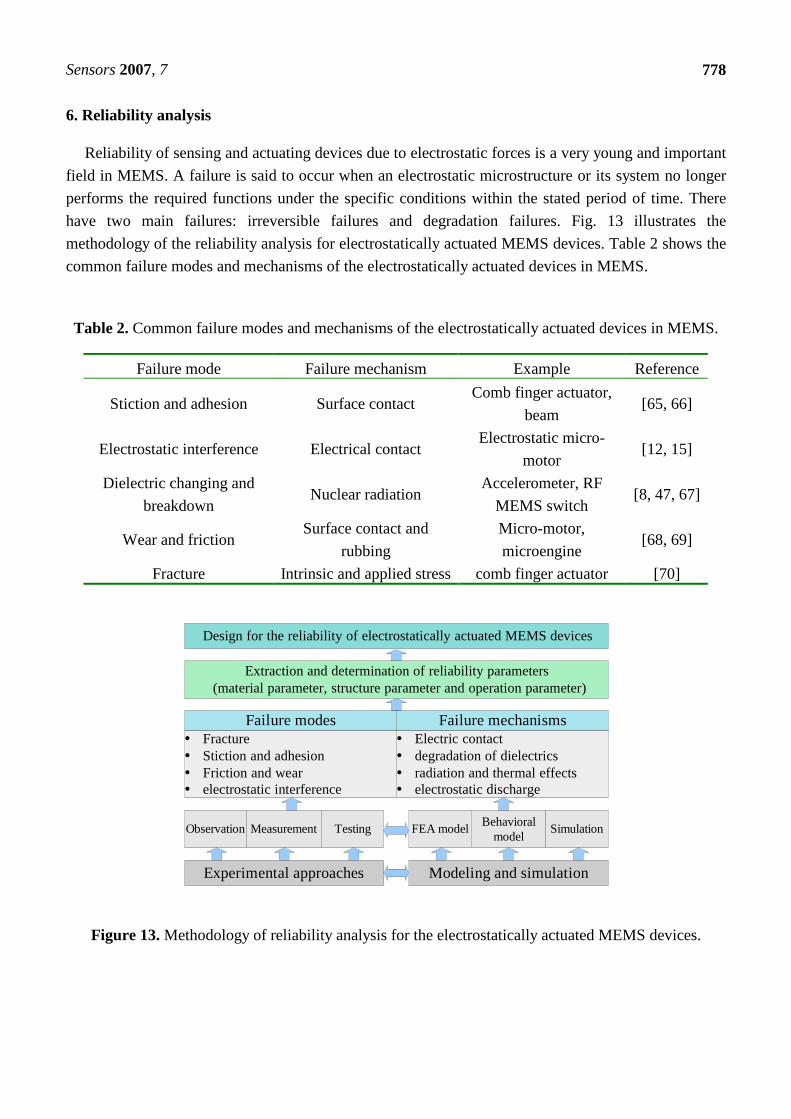
Although electrostatic forces have found many applications, they are seldom considered for the

actuation of macro-scale structures unless very high voltages are involved [1,2]. Electrostatic forces

may offer distinct advantages over more familiar actuation forces at size scales approaching microns

[3]. The electrostatic principle is common in the sensing and actuating MEMS devices and there are

many MEMS structures subjected to electrostatic forces [2,4].

Electrostatic MEMS is an important branch with a wide range of applications including sensing

devices and actuating devices in MEMS [5]. For example, the sensing devices such as capacitive

accelerometers [6] and capacitive sensors [7] are widely used. In MEMS, electrostatic forces are often

used to actuate microstructures, including switches [8,9], micro-grippers [10], micro-relays [11],

electrostatic motors [12,13], etc. Furthermore, electrostatic forces are extensively used both in linear

and rotary motors [12-14]. For an electrostatic micro-actuator with liner motion, it has been proposed

parallel, quad, and comb types of actuators. Electrostatic micro-motors are classified as top-drive, side-

drive, and wobble types [12,14-15], etc. Other examples of electrostatic micro-actuators are

electrostatic film actuator, insect type micro robot, and air levitated electrostatic actuator system [14].

The use of electrostatic actuation in MEMS is attractive because of the quite efficient, high energy

densities and large forces available for MEMS devices in micro-scale [16]. Moreover, electrostatic

actuators have advantages of inherent simplicity in their design, fast response, the ability to achieve

rotary motion, and low power consumption. The fabrication of electrostatic actuators is compatible

with integrated circuit (IC) processes in contrast to other actuators [2]. In addition, the most successful

commercialized examples are the electrostatically actuated inkjet head applied in inkjet printers and the

digital micro mirror array applied in optical scanner and digital light projectors [4].

Unfortunately, microstructures undergo large deformation when subject to electrostatic actuation

and the interaction between a nonlinear electrostatic force and the coupled effects from different energy

fields which may cause pull-in instability and failures (stiction, wear, dielectric changing and

breakdown etc.) in many electrostatically actuated MEMS devices. As a consequence of the popularity

and utility of electrostatic MEMS, many aspects of effects subject to electrostatic forces in MEMS

devices have been investigated in recent years. Researchers have studied the pull-in instability [17-20],

characteristics of the displacement during actuation [16,21-23], shape and location of electrodes

[24-26], dynamic response and optimization of the electrostatic force [9,27], nonlinear dynamics, chaos

and bifurcation of the electrostatically actuated systems and analysis methods (FEM, FDM and FCM,

etc.) for evaluating the nonlinear electrostatic forces [28-32], simulation software and systems

(ANSYS, ABAQUS, COULOMB, MEMCAD system and Macromodel, etc.) to simulate the dynamic

behaviors [31,33-35], influence of bonding parameters (applied voltage, temperature, etc.) on the

electrostatic force [36], inherent nonlinear and stiffness softened effects [4,28], failure modes and

mechanisms, materials selection and reasonable design, etc. in the aspects concerning reliability

[15,17,37-42] in MEMS. Without an understanding of the effects of electrostatic forces in MEMS,

many phenomena of practical importance, such as instability, nonlinearity and reliability in MEMS

cannot be explained scientifically, and consequently the great potential of MEMS technology could

neither be explored effectively nor utilized optimally. Therefore, it is important and necessary to

Sensors 2007, 7

762

investigate the dynamic characteristics of the electrostatic force and its nonlinear effects on MEMS

devices in micro-scale.

In this paper, a detailed review and analysis of the important electrostatic force in MEMS, its

physical model, scaling effect, stability, nonlinear dynamics and reliability are depicted. It has the

following structure. In section 2, the physical model is described for the analysis of electrostatic forces

usually applied in MEMS. In section 3, the scaling effect on the electrostatic force in micro-scale is

probed. In section 4, pull-in instability is investigated, the effects of the effective stiffness, dielectric

charging, stress gradient and temperature on the pull-in voltage are discussed and several methods to

extend the controllable travel range are suggested. In section 5, the nonlinear dynamic behaviors of a

system under the effects of inherent nonlinearity, stiffness softened and their coupled nonlinear

characteristics are studied. Different kinds of failure modes and mechanisms and methods to reduce the

failures in electrostatically actuated MEMS devices are discussed in detail in section 6. Finally, the

paper is ended in section 7 with conclusions.

2. Physical model

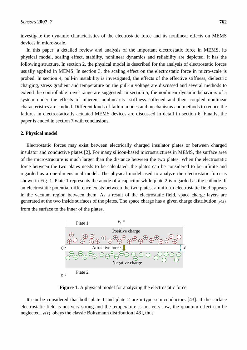
Electrostatic forces may exist between electrically charged insulator plates or between charged

insulator and conductive plates [2]. For many silicon-based microstructures in MEMS, the surface area

of the microstructure is much larger than the distance between the two plates. When the electrostatic

force between the two plates needs to be calculated, the plates can be considered to be infinite and

regarded as a one-dimensional model. The physical model used to analyze the electrostatic force is

shown in Fig. 1. Plate 1 represents the anode of a capacitor while plate 2 is regarded as the cathode. If

an electrostatic potential difference exists between the two plates, a uniform electrostatic field appears

in the vacuum region between them. As a result of the electrostatic field, space charge layers are generated at the two inside surfaces of the plates. The space charge has a given charge distribution )(zρ

from the surface to the inner of the plates.

Positive charge

Negative charge

Plate 1

Plate 2

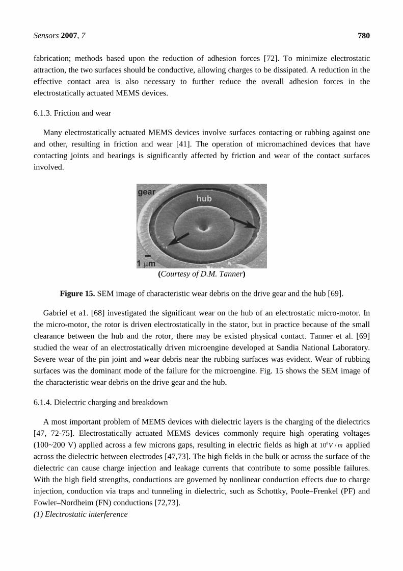
0 Attractive force d

z

0V

Figure 1. A physical model for analyzing the electrostatic force.

It can be considered that both plate 1 and plate 2 are n-type semiconductors [43]. If the surface

electrostatic field is not very strong and the temperature is not very low, the quantum effect can be neglected. ( )ρ z obeys the classic Boltzmann distribution [43], thus

Sensors 2007, 7

763

0 0( ) / ( ) /( ) 1 1z B K z B Kq V V k T q V V k Tb bρ z q n e p e− − − = − − − (1)

Where q is the elementary charge, bn and bp are the equilibrium densities of holes and electrons,

respectively, zV is the electrostatic potential at the point Z , 0zV V− is the potential difference between

point Z and the inside of the semiconductor plate 1, Bk is the Boltzmann constant and KT is the

temperature in Kelvin.

At the surface of one plate, one-dimensional Poisson equation can be given by

2

20

( )

r

d V ρ z

ε εdz= − (2)

Where 0ε and rε are the permittivity of vacuum and the relative permittivity of the material,

respectively. The electrostatic field can then be obtained [43]

( ) ( )0 0

1/ 21/ 2

0 0 02

( ) ( )( ) 2 1 1

q V V q V Vz zk T k TB K B Kr B K z zB K

f b bB K B K

ε ε k T q V V q V Vk TE z n e p e

q k T k Tq

− − −−

− − = − − − + −

(3)

After the electrostatic field is found, the electrostatic force can be easily calculated by

2

0

1

2e fF ε AE= (4)

Where fE is the electrostatic field, A is the surface area of the plates.

3. Scaling effect

It is useful to understand how forces scale in the design of micro-sensors and micro-actuators [14,

44-45]. To explain the scaling effects on electrostatically actuated MEMS devices, Trimmer’s analysis

of the scaling of a simple parallel plate capacitor can be followed [44]. The size of the system is

represented by a single scale parameter L , which describes the linear scaling of the system and the

choice of it for a system is arbitrary. However, all dimensions of the system are equally scaled down in

size as L is decreased if L is chosen. Table 1 shows the dimensions of several forces in micro-scale

[14,45]. As shown in Table 1, each force has different dimension, and is affected differently by

miniaturization.

Electrostatic forces become significant in micro-domain and have numerous potential applications in MEMS. The exact form of the scaling of electrostatic forces depends upon how the fE field changes

with size. Generally speaking, the breakdown electric field fE of the insulator increases as the system

becomes smaller. For the constant electric field ( 0[ ]fE L= ) the electrostatic force scales as 2[ ]L . When

fE scales as 1/ 2[ ]L− , then the electrostatic force has the even better scaling of 1[ ]F L= .

Since electrostatic forces are generated between the approaching objects, there is no application for

the conventional actuator except for the micro-actuator in MEMS [14]. In MEMS, electrostatic forces

influence the objects effectively when they approach each other gradually. Because of that and the

Sensors 2007, 7

764

scaling effect, an electrostatic micro-actuator is suitable for actuation and is easy to miniaturize.

However, the issue of using the electrostatic force as the driving force is that high voltage is needed to

generate it. Electrostatic force eF can be obtained from Equation (4) and is represented by the following

formulation listed in Table 1.

2

0 2

1

2e

VF ε A

d= (5)

Where V is the applied voltage, d is the distance of gap between the two plates. Dimension of

Equation (5) can be represented by

[ ]2 2

2 2 00 0 02 2

1 1 [ ] 1

2 2 2[ ]e

V LF ε A ε V ε V L

d L

= = ⋅ = ⋅ (6)

Table 1. Scaling effects on the dimension for different kinds of forces.

Force Formulation Scaling Description

20

1

2e fF ε AE= [ ]2L fE : electric field strength 0ε :

permittivity A : surface area

(Normal) Electrostatic force

2

2

02

1

d

VAεFe = [ ]0L

V : applied voltage d : gap

(MEMS)

Electromagnetic

force cm A

µ

BF

0

2

2= [ ]2L

0µ : permeability B : magnetic

density

cA : area of cross section of coil

Piezoelectric force L

ELEAFp

)(∆= [ ]2L L : length E : Young’s modules

L∆ : strain

Lorentz force )( BLIFL ×= [ ]2L I : current density

Thermal expansion

force

∆ ( )t

L TF EA

L= [ ]2L

L : length E : Young’s modules

∆L : strain T : temperature

Inertial force 2

2

t

xmFi ∂

∂= [ ]3L m : mass t : time x :

displacement

Viscosity force t

x

L

AcF vv ∂

∂= [ ]2L vc : viscosity coefficient A :

surface area t : time x :

displacement

Elastic force L

LEAFel

∆= [ ]2L L : length E : Young’s modules

L∆ : strain A : cross section area

Friction force NµF f = [ ]2L µ : friction coefficient N :

normal force

Sensors 2007, 7

765

From Equation (5), it is noticed that it is the electrostatic field rather than high applied voltage that

is responsible for the effect of the electrostatic force. In small volume, extremely high electrostatic

field can be obtained, though the total voltage drop may be deceptively small [2]. Equation (6) shows

that electrostatic force is generated in proportion to 2/ dA , i.e. 0[ ]L . If 2/ dA is a constant in

miniaturizing the electrostatically actuated MEMS devices, the electrostatic force generated has no

change. Therefore, the electrostatic force can be suited as the driving force for the micro-actuators in

MEMS.

A large displacement in an electrostatic micro-actuator element can be achieved only if the actuator

moves parallel to the capacitor plate. The electrostatic force between the two plates includes two parts

in two directions, i.e. the perpendicular electrostatic force ( epF ) and the tangential electrostatic force

( etF ), can be given by [45]

2

20 02

1 1

2 2ep f

abVF ε ε AE

d= = (7)

and

2

20 0

1 1

2 2et f

bVF ε ε bdE

d= = (8)

Where a and b are the lateral dimensions of the poles. These forces depend on the voltage that can be put across the electrodes. On a macroscopic level,

the breakdown strength of a gas is assumed to be constant and is about cmkV /30 for air at room

temperature and atmospheric pressure [45]. When scaled, the electrostatic force will change with a

factor 2[ ]L (the electric field is supported to be constant). At very small distances, the breakdown

voltage even increases again. At atmospheric pressure, the minimum breakdown voltage is V350 at

mµ8 [45].

4. Stability analysis

4.1. Pull-in effect

A major problem is the well-known pull-in instability resulted from electrostatic forces, which tends

to limit the stable travel range of many electrostatic micro-sensors and micro-actuators [16, 18, 46].

Pull-in voltage is one of the basic parameters in the design of many electrostatically actuated MEMS

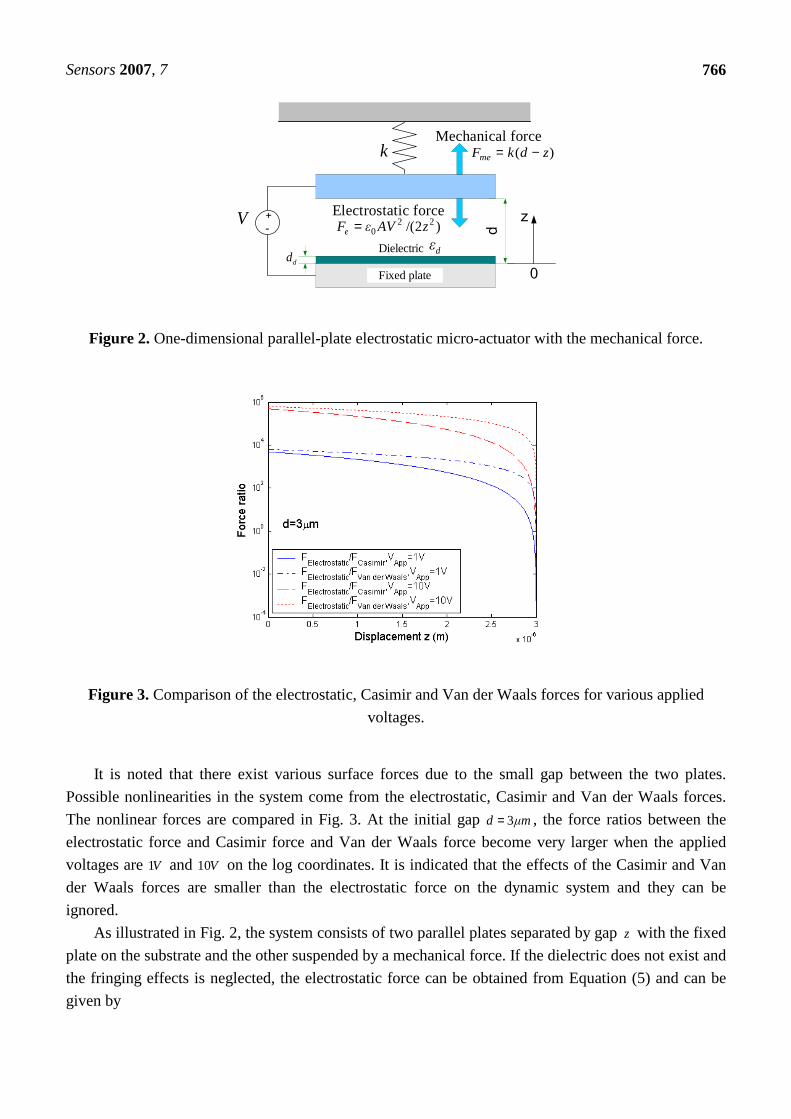
devices [5, 18]. In order to illustrate this phenomenon, a simplified typical variable capacitor model for

the analytical description of electrostatically micro-actuators is shown in Fig. 2.

Sensors 2007, 7

766

z

0

+-

V

d

k

)2/( 220 zAVεFe =

Fixed plate

Electrostatic force

Mechanical force)( zdkFme −=

ddDielectric dε

Figure 2. One-dimensional parallel-plate electrostatic micro-actuator with the mechanical force.

Figure 3. Comparison of the electrostatic, Casimir and Van der Waals forces for various applied

voltages.

It is noted that there exist various surface forces due to the small gap between the two plates.

Possible nonlinearities in the system come from the electrostatic, Casimir and Van der Waals forces.

The nonlinear forces are compared in Fig. 3. At the initial gap mµd 3= , the force ratios between the

electrostatic force and Casimir force and Van der Waals force become very larger when the applied

voltages are V1 and V10 on the log coordinates. It is indicated that the effects of the Casimir and Van

der Waals forces are smaller than the electrostatic force on the dynamic system and they can be

ignored.

As illustrated in Fig. 2, the system consists of two parallel plates separated by gap z with the fixed

plate on the substrate and the other suspended by a mechanical force. If the dielectric does not exist and

the fringing effects is neglected, the electrostatic force can be obtained from Equation (5) and can be

given by

Sensors 2007, 7

767

2

2

02

1

z

VAεFe = (9)

The electrostatic force is nonlinear because it depends on 2/1 z , while the elastic restoring force,

)( zdkFme −= , is linear with z , where k is the stiffness of the spring.

The distance z at different voltages is obtained from the balance between the electrostatic force and

the mechanical force, i.e. mee FF = , then it satisfies

02

2023 =+−

k

AVεdzz (10)

From Equation (10), we can set it in the inverse form and give the following equation

)(2

)( 2

0

zdzAε

kzV −= (11)

Analyzing Equation (11), we can obtain that the function )(zV reaches its maximum value inpullV − at

3/2dzz inpull == − , i.e.

3

027

8d

kV inpull =− (12)

Figure 4. Electrostatic micro-actuator deflection as a function of the applied voltage.

With the values of k and d , which the reference state is mFε /1085.8 120

−×= , mNk /17.0= , mµd 3= , 29106.1 mA −×= [28,29], the pull-in voltage is calculated as VV inpull 8.9=− . Fig. 4 displays the relationship

between the electrostatic deflections and the applied voltages. For voltages inpullVV −< (i.e., at distance

inpullzz −> ) the upper plate resides in a stable region. For inpullVV −> (i.e., at distance inpullzz −< ) the elastic

suspended plate collapses towards the opposite plate, and resides in the unstable region.

Sensors 2007, 7

768

Pull-in instability occurs as a result of the fact that the electrostatic force increases nonlinearly with

decreasing gap ( 2−∝ zFe ), whereas the mechanic force is a linear function of the change in the gap

( )( zdFme −∝ ). The equilibrium position of the plate may be found by equaling the electrostatic and

mechanical forces. As V increases, the gap distance at first decreases gradually. However, at a critical

voltage value (i.e. pull-in voltage), a bifurcation occurs, and the plate suddenly collapses. The

maximum stable deflection of the plate before pull-in is 1/3 of the undeflected gap d .

4.2. Effects on the pull-in voltage

4.2.1. Effect of effective stiffness effk

The analysis for estimating effective stiffness effk of the spring is simplified to a large range due to

the absence of axially induced forces [5]. A micro-cantilever beam is subjected to a distribution load

over a partial length pL originating from the tip of the beam. The stiffness of the spring seen at the

point of the maximum displacement [5], i.e. at the free end, is easily evaluated and is given by

* 3

3 3

2 3

3 8 6effr r

E bhk

L λ λ

= − +

(13)

Where /r pλ L L= , b , h and L are the width, depth and length of the micro-cantilever beam,

respectively. The effective Young’s modulus *E is equal to E for hb ≈ , and equal to the plate modulus 2/(1 )E υ− for 5b h> , υ is the Poisson ratio.

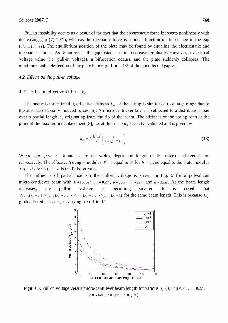
The influence of partial load on the pull-in voltage is shown in Fig. 5 for a polysilicon

micro-cantilever beam with GPaE 160= , 27.0=υ , mµb 50= , mµh 1= and mµd 3= . As the beam length

increases, the pull-in voltage is becoming smaller. It is noted that

( 0.1) ( 0.3) ( 0.5) ( 1)pull in r pull in r pull in r pull in rV λ λ V λ V λ− − − −= > = > = > = for the same beam length. This is because effk

gradually reduces as rλ is varying from 1 to 0.1.

Figure 5. Pull-in voltage versus micro-cantilever beam length for various rλ ( 160E GPa= , 27.0=υ ,

mµb 50= , 1h µm= , mµd 3= ).

Sensors 2007, 7

769

4.2.2. Effect of dielectric charging

If the effect of the interfacial charge pσ at the air dielectrics interface in the electrostatically actuated

model shown in Fig. 2 has been considered, it has been proven that the pull-in voltage of the cantilever

beam will have to increase to compensate for the field reduction in the air gap due to the interface

charge. The voltage offset offsetV due to the parasitic charge can be expressed as [47]

poffset d

d

σV d

ε= − (14)

This offset is best determined by calculating half the difference between the absolute values of the

positive and negative pull-in voltage. Thus, sensors and actuators are subject to an additional

electrostatic force depending nonlinearly on the applied voltage and the displacement. The pull-in

voltage with the effect of the interface charge can be given by [48]

2

0

2 2

3 3d

pull ind

dkV d d

ε A ε−

= +

(15)

Where dd , dε are the thickness and the relative permittivity of the dielectric, respectively.

It is indicated that the effect of the interface charge is to shift the pull-in voltage. The increase of the

pull-in voltage can be explained by the accumulation of charges in the dielectric. They create a

parasitic electric field that superposes the electric field created by the applied actuation voltage.

4.2.3. Effect of stress gradient

The release of a cantilever beam from the substrate can lead to an important beam curvature if stress

is not homogenous over the thickness direction. This gradient of stress over the thickness direction

causes a moment that results in a maximum deflection, the deflection can be written as [49]

2

max

2

L σz

E= (16)

Where maxz is the maximum beam deflection, σ is the stress. The deflection of the micro-cantilever

beam can be easily measured by optical profilometers or microscopes.

Rocha et al. [50] introduced the in plane 0.2 /MPa µm stress gradient in the actuator capacitor model

to check its effect on the pull-in voltage. Since the stress gradient causes bending, the electrostatic

force is not in equilibrium and there is a small initial deflection of the micro-cantilever beam. In this

case, the pull-in voltage shifts to a lower value than that previously calculated.

4.2.4. Effect of temperature

The pull-in voltage shows a temperature coefficient [50]. The source of the temperature dependence

of the pull-in voltage appears to be the thermal expansion of the materials and the dependence of

Sensors 2007, 7

770

Young’s modulus on the temperature. Both properties change the mechanical spring of the system,

leading to changes in the voltage required to get the critical deflection.

If a simple analysis is performed concerning the thermal effect on the micro-cantilever beam, the

spring stiffness k is represented as the temperature dependent part [51]. The relationship between the

temperature T and the spring stiffness k can be expressed as

[ ]( ) 1 ( )k T k α β T= + + (17)

Where α and β are the thermal expansion coefficient and the Young’s modulus thermal coefficient,

respectively. For the polysilicon structure, the thermal expansion coefficient is 6 13 10α K− −= × and the

Young’s modulus thermal coefficient is 6 167 10β K− −= − × [50,51].

Substituting Equation (17) into Equation (12) and taking the derivative to temperature, the

following expression can be yielded by

[ ] [ ]

31/ 2 1/ 2

0

8

27 2 1 ( ) 2 1 ( )

pull inpull in

V k α β α βd V

T ε A α β α β

−−

∂ + += ⋅ = ⋅∂ + + + +

(18)

From Equation (18), it can be seen that the pull-in thermal efficient is nonlinear, and that it increases

with the temperature. For example, there are two opposite effects acting on the pull-in voltage of the

RF switch [49]. Firstly, the bridge dilates with the increase of temperature, the gap increases and thus

also the pull-in voltage. Secondly, the Young’s modulus decreases with increasing temperature,

therefore the bridge’s stiffness and consequently the pull-in voltage decrease. Rocha et al. [52]

presented a two DOF analytical pull-in model to verify the effect of the temperature on the pull-in

voltage. Introducing 6 13 10α K− −= × and 6 167 10β K− −= − × , the relationship between the temperature and

the pull-in voltage can be obtained. The pull-in voltage has been computed between 0 and 40 Co and

yielded a 0.5 /mV K− temperature coefficient [50]. Moreover, Tada et al. [53] reported that the Young’s

modulus temperature coefficient contains quadratic and higher terms in addition to the linear

coefficient β .

4.2.5. Extending the travel range

Although the electrostatically actuated MEMS devices are widely used, they are inherently limited

in the travel range due to stable actuation is achievable only over one third of the gap between the

plates. Therefore, it is desirable to increase the travel range of the electrostatically actuated MEMS

devices beyond the 1/ 3 limit.

Design trade-offs have to be made between force, displacement and applied voltage requirements

for extending the travel range. Several methods have been suggested to extend the controllable travel

range by optimizing the structural design [16], by incorporating an on-board folded capacitor on the

device [22], by using a multiphase piecewise linear mechanical flexure [54], by external electrodes

[55], and by adding additional circuitry [56]. A control law was proposed in [57] for linearizing an

electrostatic actuator. Sun et al. [58] presented experimental results using a nonlinear model to extend

the travel range without additional hardware and device area and further complicate fabrication

Sensors 2007, 7

771

processes. In attempts to extend the controllable regime for device actuation, designers have

implemented a zipping approach to electrostatic design [59], also demonstrated with curved laterally

displaced electrostatic cantilever devices [60]. Moreover, charge control [61], which is opposed to

voltage control, becomes one effective way to extend the stable range of actuation.

For example, Hung et al. [16] investigated the pull-in instability and presented the leveraged

bending and strain-stiffening methods for extending the stable travel range of electrostatic actuators

beyond 1/3 of the pull-in instability limit for parallel-plate electrostatic actuators. The leveraged

bending method is to reduce the pull-in instability by applying electrostatic force to only a part of a

structure, then using the rest of the structure as a lever to position specific parts of the structure through

a large range of motion. As shown in Fig. 6, the leveraged bending method is applied to a simple

electrostatically actuated beam. In this case, the beam can move the larger gap, even if the part of the

beam that is being electrostatically actuated moves 1/3 of the gap or less. The leveraged bending effect

can be used to maximize the travel range of an electrostatic micro-actuator for a given gap size,

achieving up to full gap travel at the cost of increased actuation voltage.

VF

Large stable deflection

VF

Large stable deflection

F

(a)

(b)

Figure 6. Leveraged bending method to extend the stable travel range of an electrostatic micro-

actuator: (a) cantilever beam; (b) doubly clamped beam.

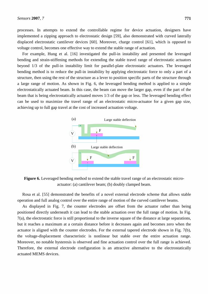
Rosa et al. [55] demonstrated the benefits of a novel external electrode scheme that allows stable

operation and full analog control over the entire range of motion of the curved cantilever beams.

As displayed in Fig. 7, the counter electrodes are offset from the actuator rather than being

positioned directly underneath it can lead to the stable actuation over the full range of motion. In Fig.

7(a), the electrostatic force is still proportional to the inverse square of the distance at large separations,

but it reaches a maximum at a certain distance before it decreases again and becomes zero when the

actuator is aligned with the counter electrodes. For the external tapered electrode shown in Fig. 7(b),

the voltage-displacement characteristic is nonlinear but stable over the entire actuation range.

Moreover, no notable hysteresis is observed and fine actuation control over the full range is achieved.

Therefore, the external electrode configuration is an attractive alternative to the electrostatically

actuated MEMS devices.

Sensors 2007, 7

772

Substrate

Dielectric

External electrodeCantilever beamClamped end

a b

Figure 7. Schematic diagrams of the micro-cantilever beams: (a) external electrode; (b) and tapering

external electrode.

5. Nonlinearity analysis

5.1. Resonance response

The electrostatic force has a square dependence on the applied voltage 21

)]cos([ 0 tωVV = , in order to

isolate the parametric effects from harmonic effects, we can use a square rooted sinusoidal voltage

signal. We presented a modified nonlinear Mathieu equation for the electrostatically actuated system

[28] shown in Fig. 2, i.e.

)()()()(),( 0 tpxetqxfxxxψx =⋅++++ &&& (19)

Where xζxxψ && =),( , 0)(0 =xf , 0( ) Ψ cosΩq t V t= , 232)( xxxe −−= , 0( ) Ψ cosΩp t V t= , 0Ω /ω ω= , /ζ c km= ,

0 /ω k m= and 02 3

0

Ψ2

ε A

mω d= .

Using the harmonic balance (HB) method, the relationship between the amplitude a and the

dimensionless frequency *a can be given by

*

2 2 202 *2 2 3 *2 2

Ψ ΩΨ( ) ( )Ω Ω Ω

Va Va

a ζ a ζ= +

+ + (20)

Where Ψ and ζ are the dimensional variables, Ω is the resonant parameter.

Sensors 2007, 7

773

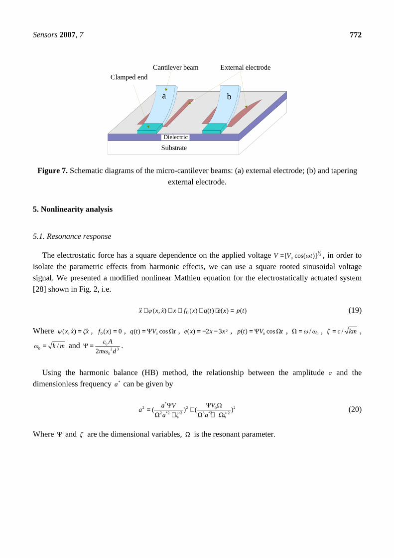
Figure 8. The relationship between the amplitude a and the frequency *a of an electrostatically actuated system in MEMS when umumumd 5,3,1= with VV 100 = and 1=Ω .

The relationships between the amplitude a and the frequency *a under different applied voltages

and various gaps between the plates are illustrated in Fig. 8. As showed in Fig. 8, the amplitude a

reduces quickly and tends to an approximation when the gap between the plates is becoming wider (e.g., 005.0≈a at umd 5= with 1=Ω and VV 100 = ). Therefore, the gap d and the applied voltage 0V are

the main factors for the measurement and detection of the displacement of an electrostatically actuated

system in MEMS.

5.2. Inherent nonlinear effect

It is known that the dynamic characteristics of a system depend on the operational parameters,

geometrical dimensions and material properties [4]. However, for an electrostatically actuated system,

the electrostatic force will change the dynamic characteristics of structures and as the structure

deforms, the electrostatic force redistributes, thereby modifying the mechanical loads.

Expanding the nonlinear electrostatic force term ))(2/( 220 zdAVε − in Equation (9) by Taylor series

with respect to the equilibrium position, i.e. 0=z , gives

)32

1(2

1

)(2

1 2

22

2

02

2

0 L+++⋅=−

⋅ zd

zdd

VAε

zd

VAε (21)

Based on the small displacement assumption, the higher order terms can be neglected, thus the

nonlinear electrostatic force can be linearized as

)22

1(2

1

)(2

1 2

22

2

02

2

0 zd

zdd

VAε

zd

VAε ++⋅=

−⋅ (22)

Sensors 2007, 7

774

Introducing the dimensional vector TT xxxx ],[],[ 21 &= , the state space representation of the

electrostatically actuation model gives a nonlinear, parametric and forcing excitations, time-varying

and T-periodic model, i.e.

21

22 1 1 1 0 02 (2 3 )Ψ cosΩ Ψ cosΩ

xx

ζx x x x V t V tx

=

− − + + +

&

&

(23)

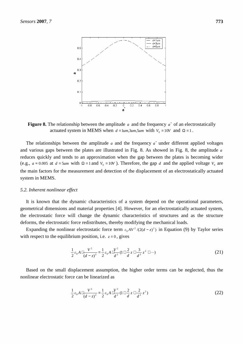
Figure 9. phase portrait and Poincare map of the nonlinear dynamic system with VV 200 = , 1=Ω and

umd 3= , the simulation is scaled in time with relation 0tωt = for numerical integration accuracy.

The phase portrait of the system is a representation of all its trajectories. Fig. 9 illustrates the phase

portrait to investigate the nonlinear dynamical behaviors of the system. It can be found that the phase

portrait at 1=Ω is a two-dimensional close loop and its stable equilibrium is a fixed point A (in

Poincare plane) for trajectory in phase space. Therefore, the system is stable for different resonant

parameters without considering the nonlinear spring stiffness term.

5.3. Stiffness softened effect

The electrostatic force can significantly affect and soften the stiffness of a dynamic system [4, 30-

31]. Adams et al. [30] utilized a combination of two or more electrostatic actuators to produce linear,

quadratic, cubic, and higher order stiffness. He also carried out experiments focused on determining the

electrostatic stiffness produced using different tuning voltage combinations and obtained the result that

the electrostatic stiffness is roughly inversely proportional to the gap squared. Zhang et al [31]

presented the modeling, analysis, and experimental verification that the nonlinear effect of the cubic

electrostatic stiffness changes the dynamic behavior of the system.

To analyze the stiffness softened effect on the dynamic system, the modal expansion method [4] can

be used to discretize the governing equation of the dynamic system and the modal stiffness ′jk can be

obtained

Sensors 2007, 7

775

4

2200

3

2200

2

)(cos3)(cos

d

tAV

d

tAVkkkk jsjj

ωεωε−−′=−′= (24)

Figure 10. Changes of the first and second modal stiffness.

Equation (24) shows that the modal stiffness jk is a periodically time-varying function depending

on the applied voltage. It is indicated that the electrostatic force soften the modal stiffness of the

microstructure periodically. Numerical simulations and results of the changes of the first and second

modal stiffness 1k and 2k are illustrated in Fig. 10.

As can be seen in Fig. 10, the modal stiffness decreases periodically with the frequency ω of the

applied voltage and the variation increases with the larger magnitude 0V . Therefore, the stiffness of an

electrostatically actuated microstructure in MEMS will be softened periodically with the frequency of

the applied voltage and the variation increases with the increasing of the magnitude of the applied

voltage.

5.4. Coupled nonlinear effect

The structure-electrostatic coupling effect must be taken into account on the design of

electrostatically actuated MEMS devices. MEMS devices are often characterized by structures that are

a few microns in size, separated by micron-sized gaps. At these sizes, air damping dominates over

other dissipation. Squeeze film damping may be used to represent the air damping experienced by the

moving plates [62,63]. Starr [64] presented the expression of the damping force for a rectangular plate

of dimensions Lb 22 × as

3

23 3

16 rsfd

µc b L kF x x

x x= − = −& & (25)

Where µ is the viscous coefficient, b and L are the width and length of the beam, respectively [29].

And rc is approximately equal to

Sensors 2007, 7

776

L

Wrc 6.01−= , )10( << L

W (26)

The applied voltage is an important factor of the parallel plate capacitor which leads to coupled

nonlinearities. It is useful to understand the dynamic characteristics of the electrostatically actuated

MEMS devices by the chaotic motions of the systems due to the cubic nonlinear term. Fig. 11(a)~(d)

are the bifurcation diagrams of 0V and Poincare maps at different applied voltages without the effect of

squeeze film damping for the coupling system when the cubic nonlinear stiffness is 1 0.3k = .

Figure 11. Bifurcation diagrams of 0V for the electrostatic coupling nonlinear dynamic system and

Poincare maps under different applied voltages: (a) Bifurcation diagram of 0V ( 20PV V= );

(b) Bifurcation diagram of 0V ( 0PV V= ); (c) Poincare map (0 40V V= , 20PV V= );

(d) Poincare map (0 30V V= , 0PV V= ).

It can be seen from Fig. 11(a) that the response of the electrostatic coupling system is stable when

0V gets lower value. When 0 7.4V V> , the system response displays double periodic bifurcation:

1 2 4P P P− → − → − . Then, the system response changes between quasi-periodic and periodic motions

alternatively when 0V varies from 8.8V to 13.0V . When 0 13.0V V> , the system response becomes 1P −

(period one) motion, then shows double periodic bifurcation and enters into chaotic motion, and finally

leaves chaotic state with periodic one motion. Fig. 11(c) shows the Poincare map of the system

response at 0 40V V= . There is an isolated chaotic island in the Poincare map. It is indicated that the

system is chaotic at this time. Fig. 11(b) is the bifurcation diagram of 0V for the electrostatic coupling

dynamic system at 0PV V= . When 0 27.1V V> , the system response shows double periodic bifurcation:

1 2 4P P P− → − → − . Then, the system response alternates between quasi-periodic and periodic motions

( 6P − , 3P − , etc) in turn when 0V varies from 27.9V to 30.5V . Fig. 11(d) illustrates the Poincare map of

Sensors 2007, 7

777

the system response at 0 30V V= . It is found that a closed ring formed in the Poincare map and the

system is quasi-periodic. Therefore, the alternating current (AC) voltage and the polarization voltage

play an important role in the system responses and the responses display very rich dynamic behaviors

when these two kind of voltages change.

Squeeze film damping coefficient and ratio are the key parameters for the dynamic responses of the

MEMS devices. The larger the squeeze film damping, the louder noise will exist. Considering the

effect of squeeze film damping structural coupling with the electrostatic force on the system response,

Fig. 12(a)~(d) display the bifurcation diagrams of the damping ratio gc . It can be seen from Fig. 12(a)

that the system response changes between periodic, quasi-periodic and chaotic motion alternatively

when 0.5gc > . Then it enters into 3P − motion from chaotic state when 0.64gc > . when 0.86gc > , it

displays inverse double period bifurcation: 8 4 2 1P P P P− → − → − → − and becomes 1P − motion. With

the increase of polarization voltage, the system response changes obviously. Fig. 12(b) illustrates the

bifurcation diagram at 5PV V= . It is found that the system response displays inverse periodic

bifurcation from 2P − motion to 1P − motion, and then enters into chaotic motion when 0.58gc > .

When the squeeze film damping ratio is increasing continuously, the system response changes among

chaotic, periodic ( 4P − , 8P − and 3P − , etc.) and quasi-periodic motions alternatively. The system

response shows double periodic bifurcation (2 4P P− → − ) when 0.70gc > . When the alternating current

(AC) and polarization voltages vary simultaneously, the system responses change obviously. Fig. 12(c)

and Fig. 12 (d) are the system responses for the two combinations: 0 20V V= , 30PV V= and 0 30V V= ,

20PV V= . Therefore, the effect of squeeze film damping on the system response can not be neglected

for MEMS structures in micro-scale. The dynamic characteristics of the electrostatically actuated

MEMS devices will alter with the change of the alternating current (AC) and polarization voltages.

Figure 12. Bifurcation diagrams of gc for the electrostatic coupling nonlinear dynamic system: (a)

0 40V V= , 0PV V= , 1 0.3k = , Ω 1= ; (b) 0 40V V= , 5PV V= , 1 0.3k = , Ω 1= ; (c) 0 20V V= , 30PV V= , 1 0.3k = ,

Ω 1= ; (d) 0 30V V= , 20PV V= , 1 0.3k = , Ω 1= .

Sensors 2007, 7

778

6. Reliability analysis

Reliability of sensing and actuating devices due to electrostatic forces is a very young and important

field in MEMS. A failure is said to occur when an electrostatic microstructure or its system no longer

performs the required functions under the specific conditions within the stated period of time. There

have two main failures: irreversible failures and degradation failures. Fig. 13 illustrates the

methodology of the reliability analysis for electrostatically actuated MEMS devices. Table 2 shows the

common failure modes and mechanisms of the electrostatically actuated devices in MEMS.

Table 2. Common failure modes and mechanisms of the electrostatically actuated devices in MEMS.

Failure mode Failure mechanism Example Reference

Stiction and adhesion Surface contact Comb finger actuator,

beam [65, 66]

Electrostatic interference Electrical contact Electrostatic micro-

motor [12, 15]

Dielectric changing and

breakdown Nuclear radiation

Accelerometer, RF

MEMS switch [8, 47, 67]

Wear and friction Surface contact and

rubbing

Micro-motor,

microengine [68, 69]

Fracture Intrinsic and applied stress comb finger actuator [70]

Design for the reliability of electrostatically actuated MEMS devices

Extraction and determination of reliability parameters (material parameter, structure parameter and operation parameter)

Failure modes Failure mechanisms Fracture Stiction and adhesion Friction and wear electrostatic interference

Electric contact degradation of dielectrics radiation and thermal effects electrostatic discharge

ObservationMeasurement Testing FEA modelBehavioral

modelSimulation

Experimental approaches Modeling and simulation

Figure 13. Methodology of reliability analysis for the electrostatically actuated MEMS devices.

Sensors 2007, 7

779

6.1. Failure models and mechanisms

6.1.1. Fracture

Fracture strength, a statistical property in brittle materials such as silicon, is a function of

microstructure and processing, which can exhibit variation from run to run due to process variability

[71]. Stress in polysilicon elements should be kept to 10% or less of the measured fracture strength for

the material and process in use. Stress values in the range of several hundred MPa appear to be quite

acceptable. A completed device [70] is shown by the scanning electron micrograph SEM in Fig. 14.

(Courtesy of H. Kahn)

Figure 14. SEM micrographs of a MEMS fracture [70].

Fracture occurs when the applied load on an electrostatically actuated MEMS device is greater than

the strength of the component materials. Fracture is a serious reliability concern because it can

immediately cause catastrophic failures, particularly for the brittle materials. Therefore, it is very

important to know the mechanical properties of the materials and microstructures in micro-scale for the

electrostatically actuated MEMS devices.

6.1.2. Stiction and adhesion

Stiction is the effect that microstructures tend to adhere to each other when their surfaces come into

contact [65,66]. Stiction and adhesion are the important and almost unavoidable problems that occur in

the electrostatically actuated devices fabricated by surface micromachining in MEMS. Surface tension

forces such as electrostatic force can pull the MEMS component into contact with the substrate

resulting in stiction failure. Other causes of stiction include shock induced stiction and voltage

overstress resulting in contact.

Stiction between the contact surfaces limits the repeatability of operation or may even prevent the

operation completely. The components of the electrostatically actuated MEMS devices are small,

therefore, the surface forces can dominate each other and cause these parts come into contact. The

surface roughness is a major influence in the stiction phenomenon [66]. Permanent adhesion arises

from the large interfacial forces (capillary, electrostatic, and van der Waals forces) compared with the

restoring force of the deflected structure. All of these forces must be manipulated if the adhesion force

is to be reduced below the mechanical restoring force.

Stiction can be prevented or reduced in several ways, which can roughly be divided into two groups:

methods based upon the prevention of physical contact between structures and the substrate during

Sensors 2007, 7

780

fabrication; methods based upon the reduction of adhesion forces [72]. To minimize electrostatic

attraction, the two surfaces should be conductive, allowing charges to be dissipated. A reduction in the

effective contact area is also necessary to further reduce the overall adhesion forces in the

electrostatically actuated MEMS devices.

6.1.3. Friction and wear

Many electrostatically actuated MEMS devices involve surfaces contacting or rubbing against one

and other, resulting in friction and wear [41]. The operation of micromachined devices that have

contacting joints and bearings is significantly affected by friction and wear of the contact surfaces

involved.

(Courtesy of D.M. Tanner)

Figure 15. SEM image of characteristic wear debris on the drive gear and the hub [69].

Gabriel et a1. [68] investigated the significant wear on the hub of an electrostatic micro-motor. In

the micro-motor, the rotor is driven electrostatically in the stator, but in practice because of the small

clearance between the hub and the rotor, there may be existed physical contact. Tanner et al. [69]

studied the wear of an electrostatically driven microengine developed at Sandia National Laboratory.

Severe wear of the pin joint and wear debris near the rubbing surfaces was evident. Wear of rubbing

surfaces was the dominant mode of the failure for the microengine. Fig. 15 shows the SEM image of

the characteristic wear debris on the drive gear and the hub.

6.1.4. Dielectric charging and breakdown

A most important problem of MEMS devices with dielectric layers is the charging of the dielectrics

[47, 72-75]. Electrostatically actuated MEMS devices commonly require high operating voltages

(100~200 V) applied across a few microns gaps, resulting in electric fields as high at 810 /V m applied

across the dielectric between electrodes [47,73]. The high fields in the bulk or across the surface of the

dielectric can cause charge injection and leakage currents that contribute to some possible failures.

With the high field strengths, conductions are governed by nonlinear conduction effects due to charge

injection, conduction via traps and tunneling in dielectric, such as Schottky, Poole–Frenkel (PF) and

Fowler–Nordheim (FN) conductions [72,73].

(1) Electrostatic interference

Sensors 2007, 7

781

Materials with high insulation resistance and field strength, such as silicon oxide and silicon nitride,

are often used for insulation in the electrostatically actuated MEMS devices. The bulk or surface of

such dielectrics can be charged up locally and they provide trap sites for positive and negative charges

both deep in the bulk and at the interfaces in multilayer stacks [47]. Parasitic charge accumulating in

the electrostatically actuated MEMS devices may alter actuation voltages and change the mechanical

behaviors. Wibbeler et al. [47] studied the effects of parasitic charges on the relationship between the

deflection and applied voltage of bulk micromachined silicon cantilever actuators and provided

measurements of the charge decay.

For example, schematic illustration of a RF MEMS switch with dielectric is shown in Fig. 16. The

beam will move downwards when subjected to the electrostatic force due to the applied voltage. The

distance between the beam and dielectric will then change. Charging can arise during handling and

operation. High applied voltage exceeding the breakdown voltage of the gap will give rise to

considerable charge deposition of the dielectric. When the dielectric is charged by the ionizing

radiation and causes a change in position of the beam due to electrostatic actuation, the device behavior

will become erratic.

Substrate

Dielectric

BeamAccumulation charge

V

Figure 16. Schematic illustration of a RF MEMS switch with dielectric.

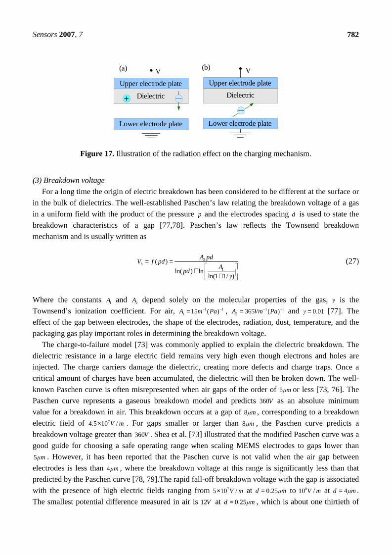
(2) Radiation effect

It is well-known that electrical systems are susceptible to radiation. The most obvious source of

dielectric charging is ionizing radiation, which can be a major problem for the application of MEMS.

Schanwald et al. [74] evaluated the mechanical and electrical performance of MEMS comb drive and

microengine actuators in the total dose radiation environments. Radiation induced charging can be

developed between the gear hub and the drive gear, and the gear pin and the drive gear [74]. Radiation

effect can aggravate the lateral and linear electrostatic clamping failures when comb drives.

The radiation effect is attributed to electrostatic force caused by charge accumulation in dielectric

layers, such as Parylene, SiO2, Si3N4, etc. To illustrate the charging mechanism, a physical arrangement

is shown in Fig. 17. The charge distribution in the dielectric produced by radiation in the presence of a

biasing voltage is complicated due to the gap between the dielectric and the lower electrode plate [75].

As illustrated in Fig. 17(a), for negative bias during radiation, secondary electrons are emitted from the

dielectric before becoming thermalized and lead to a net positive charge at the surface of the dielectric.

For positive bias during radiation, secondary electrons are emitted from the lower electrode plate are

attracted to the dielectric, as displayed in Fig. 17(b).

Sensors 2007, 7

782

Upper electrode plate

Lower electrode plate

V(a)

+ Dielectric

Upper electrode plate

Lower electrode plate

V(b)

Dielectric

Figure 17. Illustration of the radiation effect on the charging mechanism.

(3) Breakdown voltage

For a long time the origin of electric breakdown has been considered to be different at the surface or

in the bulk of dielectrics. The well-established Paschen’s law relating the breakdown voltage of a gas

in a uniform field with the product of the pressure p and the electrodes spacing d is used to state the

breakdown characteristics of a gap [77,78]. Paschen’s law reflects the Townsend breakdown

mechanism and is usually written as

2

1

( )

ln( ) lnln(1 1/ )

b

A pdV f pd

Apd

γ

= = + +

(27)

Where the constants 1A and 2A depend solely on the molecular properties of the gas, γ is the

Townsend’s ionization coefficient. For air, 1 11 15 ( )A m Pa− −= , 1 1

2 365 ( )A Vm Pa− −= and 0.01γ = [77]. The

effect of the gap between electrodes, the shape of the electrodes, radiation, dust, temperature, and the

packaging gas play important roles in determining the breakdown voltage.

The charge-to-failure model [73] was commonly applied to explain the dielectric breakdown. The

dielectric resistance in a large electric field remains very high even though electrons and holes are

injected. The charge carriers damage the dielectric, creating more defects and charge traps. Once a

critical amount of charges have been accumulated, the dielectric will then be broken down. The well-

known Paschen curve is often misrepresented when air gaps of the order of 5µm or less [73, 76]. The

Paschen curve represents a gaseous breakdown model and predicts 360V as an absolute minimum

value for a breakdown in air. This breakdown occurs at a gap of 8µm, corresponding to a breakdown

electric field of 74.5 10 /V m× . For gaps smaller or larger than 8µm , the Paschen curve predicts a

breakdown voltage greater than 360V . Shea et al. [73] illustrated that the modified Paschen curve was a

good guide for choosing a safe operating range when scaling MEMS electrodes to gaps lower than

5µm . However, it has been reported that the Paschen curve is not valid when the air gap between

electrodes is less than 4µm , where the breakdown voltage at this range is significantly less than that

predicted by the Paschen curve [78, 79].The rapid fall-off breakdown voltage with the gap is associated

with the presence of high electric fields ranging from 75 10 /V m× at 0.25d µm= to 810 /V m at 4d µm= .

The smallest potential difference measured in air is 12V at 0.25d µm= , which is about one thirtieth of

Sensors 2007, 7

783

the minimum breakdown voltage according to Paschen’s law. Moreover, Etching away the dielectric is

a very effective solution to reduce the breakdown voltage, but not to damage the electrodes [73].

(4) Lifetime prediction

Since the high field strengths required for actuation of electrostatically actuated MEMS devices, the

charging of the dielectrics become a more widespread problem. A typical dielectric of nm200 with a

voltage of V40 across it will result in the field strength of mV /102 8× [72].

The critical amount of charge when actuating with a square wave can be obtained for different

charge densities [80]. For the negative interface charge, the critical amount of charge critσ can be given

by

02 ( ) 2 ( )d d d dcrit

d

ε k d d ε d d dσ

A d

− − += − ⋅

(28)

Zafar et al. [81] calculated the amount of parasitic charge after a certain charging period for thin

high k− gate dielectric stacks. The trapped charge density ( )σ t can be written as

00

0

( )( ) 1 exp( / )

ρ τσ t N q t τ dτ

N

∞ = − −

∫ (29)

Where ( )ρ τ is the charge distribution at the time τ , q is the elementary charge, t is the charging time,

and 0N is the total trap density.

When the amount of charge is so large that the pull-out voltage crosses zero, the device will fail

[80]. The time constant for charging exponentially depends on the actuation voltage. Spengen et al.

[80] simplified the trapped charge density ( )σ t and calculated the time to failure when ( ) critσ t σ= for

SiO2 dielectric. The relationship between the actuation voltage aV and the time to failure ft can be

yielded

0

1critf a

σt V Ln

N q

= − −

(30)

(5) Methods to reduce the effects of charging

Charging of the dielectrics and the associated uncertain electrostatic forces in MEMS structures

have been a serious performance issue for many electrostatically actuated MEMS devices, such as

microphones, displays, micromirrors, and RF switches, etc. [47,73-74]. Design, modeling and

simulation that eliminate the effects of charging become more and more important.

Bochobza-Degani [61] modeled an interface charge and the modeling is too general to be easily

applicable to real MEMS devices. A most straightforward method to decrease the effect of dielectric

charging is to use a bipolar AC rather than DC voltage actuation [73]. However, the charging effect can

not be eliminated completely and more complex actuation electronics are required. The other way to

reduce the effect of the dielectric charging is by controlling the electrode and dielectric geometry,

mainly the width of the gaps with exposed dielectric between electrodes, the thickness of the

electrodes, selective etching of the dielectric and dielectric materials. Smaller gap can decrease the

Sensors 2007, 7

784

magnitude of charging induced drift and shorten the saturation time, resulting in reducing the adverse

effect of charging on mirror stability. At the same time, careful consideration of operating conditions

and trade-off design are required before deciding on the ideal gap size for a given application due to the

influences of the anodic oxidation and the breakdown voltage.

Moreover, depositing or growing a thin conductive layer on top of the dielectric in order both to

bleed off surface charge and to screen bulk charge from the reflector has been developed and applied to

MEMS devices [73]. This charge dissipation layer (CDL) must not contain charge traps and typically

consists of a thin film of a poor conductor such as a doped oxide. A Co-Fe-O film of tunable

conductance is an effective CDL for MEMS devices [73]. Rather than depositing a CDL over the

dielectric, the dielectric material itself can act as a CDL if its electrical transport properties are suitable.

For capacitive RF MEMS switches, Raytheon patented the approach of leaky SiN to control charging

[82].

6.1.5. Environmentally induced failure mechanisms

(1) Anodic oxidation

Anodic oxidation of silicon electrodes and wiring is not a novel problem, but can be an important

failure mode of non-hermetically packaging electrostatically actuated MEMS devices [73]. If moisture

exists, the adsorbed water on the surface of the dielectric between electrodes or wiring provides a

leakage path for current to flow between neighboring electrodes. Anodic oxidation in MEMS devices

had been observed [83] and the effects (relative humidity, voltage, electric field, leakage current, and

electrode geometry, etc.) of it on surface micromachined polisilicon had been performed [73,84].

Anodic oxidation occurs when there is a finite surface leakage current between electrodes on the

surface of the dielectric. The poly-Si at the anode reacts with OH- to form SiO2 [85]. The rate of anodic

oxidation is proportional to the leakage current between electrodes on the surface of the dielectric.

Relative humidity is an accelerating factor, the higher the humidity, the more water is adsorbed on the

surface, and thus the larger the surface leakage current will be. The surface leakage current increases

roughly exponentially with relative humidity and the rate of anodic oxidation scales similarly with all

other condition kept constant. Voltage is a strong accelerating factor because the leakage current is

roughly proportional to the applied voltage. The electric field is also an accelerating factor. Much more

oxidation is seen at sharp corners where the field is concentrated. Changing the gap between electrodes

or wirings from 2 to 3µm has a large effect on the rate of anodic oxidation.

Shea et al. [73] illustrated two goals to control the rate of anodic oxidation. First, MEMS chips are

designed such that anodic oxidation occurs as slowly as possible should the package leak. Second,

structures that are purposefully extremely susceptible to anodic oxidation are designed and used as

early warning devices.

(2) Electrostatic discharge

Electrostatic discharge (ESD) is an important consideration and has been observed as a failure mode

in MEMS [65, 73]. An ESD discharge can cause both electrical and mechanical damage. Possible

electrical damage from the discharge includes melted wires or electrodes, pinholes or weakened

dielectrics, and shorted transistors. While the effects of ESD on MEMS structures have not been

Sensors 2007, 7

785

published to date, it can be assumed that certain electrostatically actuated MEMS devices will be

susceptible to the ESD damage.

6.2. Approaches to failure analysis

6.2.1. Selection of materials

The principal performance and reliability metrics considered for electrostatically actuated MEMS

devices are the applied voltage, speed of actuation, actuation force, stored energy, electrical resistivity,

mechanical quality factor, and resistance to fracture, friction, shock, and stiction [38, 40, 42, 86]. The

materials properties governing these parameters are the Young’s modulus, density, fracture strength,

intrinsic residual stress, resistivity, and intrinsic material damping [38]. The material parameters of

microstructures, such as Young’s modulus and intrinsic stresses can also be given by the relationship

between the electrostatic loads and the structural deflections [17].

According to the Ashby method for the selection of materials [87], the performance of an element

can be described by the following form

),,( MGFpp = (31)

Where F , G and M represent the functional requirements, geometric parameters and material indices.

p describes the performance aspects of component such as its mass or volume, cost and life. Optimal

design is the selection of the material and geometry, maximizing or minimizing p according to its

reliability and desirability.

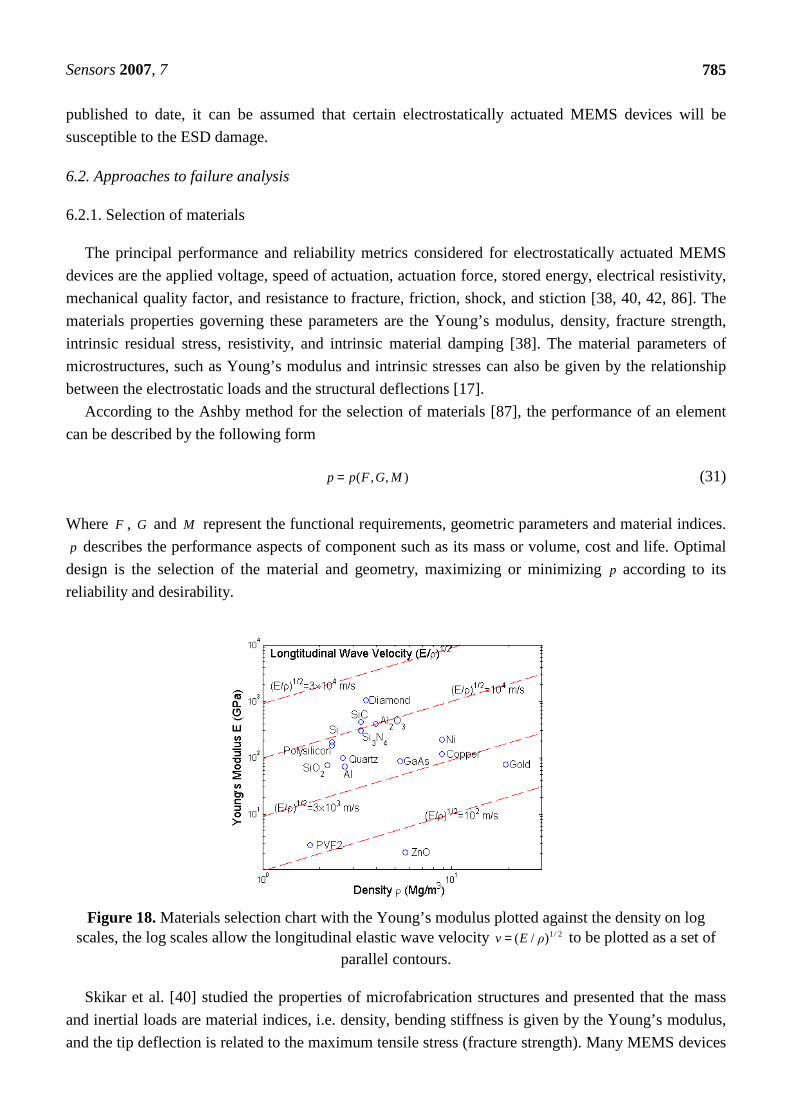
Figure 18. Materials selection chart with the Young’s modulus plotted against the density on log scales, the log scales allow the longitudinal elastic wave velocity 2/1)/( ρEv = to be plotted as a set of

parallel contours.

Skikar et al. [40] studied the properties of microfabrication structures and presented that the mass

and inertial loads are material indices, i.e. density, bending stiffness is given by the Young’s modulus,

and the tip deflection is related to the maximum tensile stress (fracture strength). Many MEMS devices

Sensors 2007, 7

786

are susceptible to the failure by electrostatically actuated stiction, which occurs when the structures are

forced into mechanical contact at operation. The higher the bending stiffness, the lower the deflection

and the probability of stiction will be. Requirements for the materials are that high 2/1)/( ρE , low ρ and

high E can be used to increase the probability of obtaining mechanical response, decrease the

magnitude of the inertial load and minimize the structural deflection, respectively.

Fig. 18 plots the relationship between the Young’s modulus E and the density ρ . Material

performance indices for several elements are referred to the literatures [42]. It can be used to make an

initial choice: diamond, silicon carbide (SiC), aluminum oxide (Al2O3), silicon nitride (Si3N4), and

silicon (Si) emerge as the attractive candidates for fabricating electrostatically actuated MEMS devices

with high resistance to stiction and adhesion.

The relationship between the Young’s modulus E and the fracture strength fσ is plotted in Fig. 19

for various microstructure materials. The nominal values shown in Fig. 19 are intended to guide the

initial choice of materials. It is indicated that materials for the large force actuators are diamond, Al2O3

and SiC, etc.

Figure 19. Materials selection chart with the Young’s modulus plotted against the fracture strength.

Material properties may significantly affect the reliability of future products because MEMS designs

become increasingly complex and the number of commercial applications is increasing [86].

Processing considerations have made silicon a popular choice as the material for the electrostatically

actuated MEMS devices, but recent advances in micromachining techniques enable the integration of a

number of different metals, alloys, ceramics, glasses, and polymers into MEMS [76]. For instance, the

materials used to fabricate electrostatic micro-motors include silicon dioxide, nickel, diamond, silicon

carbide, and polysilicon, etc. As the MEMS material sets continue to expand, it is necessary to find a

rational and systematic approach to the selection of materials in the design of electrostatically actuated

MEMS devices.

Sensors 2007, 7

787

6.2.2. Modeling and simulation

The analysis of components in the MEMS design is often based on FEA. FEA is able to couple

different physical domains (mechanical, thermal, electrical and piezoelectric, etc). In our previous work

[88], the coupling effect of mechanical and piezoelectric domains on a micro-cantilever beam was

studied and discussed. Part mode shapes of a beam (the length, width and thickness are 500µm , 30µm

and 3µm for a SiO2 beam, respectively) using finite element simulation are shown in Fig. 20.

Figure 20. Part mode shapes of the beam using finite element simulation.

Although there are many designs which use piezoelectric, thermal and magnetic actuations, so far

the most popular approach is to use electrostatic forces to move micromachined parts [33].The design

of an electrostatically actuated device in MEMS is of great important. The fabrication of an

electrostatic micro-actuator is becoming technologically feasible, but is extremely difficult, so that the

mathematical modeling of the actuator design is likely to be very important in the advancement of this

technology. Price et al [3] reviewed the basic elements of the electrostatic devices (conductors,

dielectrics, insulators, electrets and ferroelectrics) and shown that the modeling of the electrostatic

force is very different, and in many ways a more difficult undertaking than the modeling of a magnetic

interaction. Models must take into account the realities of materials, in particular the fact that the

resistivity is never infinite, and that any structural part of an actuator will affect fields through its

dielectric.

Designs of MEMS devices which use the electrostatic forces as the actuated forces are complicated

due to the fact that the dynamic characteristics of structure elements will be changed by the

electrostatic forces and that as the structure deforms, the electrostatic forces redistribute, thereby

modifying the mechanical loads [4]. Consequently, the structure-electrostatic coupling effect becomes

an important issue on the design of such structures in MEMS.

Zhang et al. [37] presented a mathematic model and FE model to calculate the area of contact and

stresses and strains in the contact region between the rotor and the bearing hub in an electrostatic

micro-motor under the effect of electrostatic forces. The stress and strain distributions under different

applied voltages are illustrated in Fig. 21 and Fig. 22. Fig. 21 shows the stress distributions in z

direction at 100U V= . On the conditions of gap unchanged and maximum gap changed, the stresses are

changing continuously. The maximum stresses are about 6 23.9 10 /N m× at 0z = in z direction. In

addition, the stresses in different scope and their distributions are similar to dissymmetrical and

symmetrical ellipses. As shown in Fig. 22, the strains are symmetric concerning the axis and the

distributions are close to half ellipses. The strains get the maximum values at 0=z , while obtaining the

minimum at their maximum contact widths. Additionally, under different applied voltages, the strains

are different and in direct proportion to the applied voltages, and similar to the stresses. When the rotor

Sensors 2007, 7

788

bushing wears against the dielectric substrate, the gradient curve of the contact pressure distribution in

the contact region can be illustrated in Fig. 23. The contact pressure displays an axis-symmetry

parabolic distribution and the results satisfy the general rules of the theoretical solutions. It is indicated

that the FE model is reasonable to model the contact behavior between the rotor bushing and the

ground plane in electrostatic micromtors.

Figure 21. Stress distributions in z directions under the effect of gap (100U V= ).

Figure 22. Strain distributions under different applied voltages.

Figure 23. Gradient curve of contact pressure distribution in the contact region.

Sensors 2007, 7

789

As driven systems, rotating electrostatic micro-motors are fabricated by surface micromachining

using polysilicon with a thickness of only a few micrometers. Except for the reasonable design and

effective modeling and simulation, many different microfabrication processes can then be applied for

fabricating various electrostatic micro-motors. The polysilicon center pin process, polysilicon flange

process, selective CVD tungsten process, Diamond-like Carbon (DLC) process, LIGA process with

sacrificial layer, and three-mask tungsten process have been published for the fabrications of

electrostatic micro-motors [13, 89].

In addition, Modeling and simulation of the electrostatically actuated MEMS devices play an

important role in the design phase in predicting device characteristics [5]. For instance, the device

models help the designers in identifying the regions of stable operation and in understanding the causes

of instabilities.

6.2.3. Experimental techniques

This section focuses on the main experimental techniques that are suitable for studying the

reliability of MEMS devices. The primary techniques, including observation, measurement and testing,

are explained and discussed.

(1) Observation

Observation techniques are important to observe the contours, images, sizes, and arrangements of

MEMS structures. Lafontan et al. [49] presented the conventional and new observation techniques,

such as optical inspection (bright field illumination, dark field illumination and Normarsky contrast

visualization), scanning electron microscopy (SEM), transmission electron microscopy (TEM), FIB-

TEM, confocal IR imaging, and full field optical profilometer and vibrometer, etc. FIB, parallel

polishing, lift-off and laser ablation have been developed and applied to MEMS sample preparations.

FIB preparation uses the ion beam to image the sample and to remove material from both sides of

the desired section [49, 69, 72, 90]. In the FIB, the material removal is monitored in real time. Pre-

thinning and lift out are the two approaches to FIB sample preparations and the cross-section of an

unreleased electrostatic micro-motor realized in MUMPs [49, 90]. In such a design, the size of the

oxide layers controls the mechanical clearance between the rotor and the hub. The gap between the

rotor and the hub is approximately 15% thinner than the standard layer thickness. It is important for the

designer to calculate the capacitive electrostatic force with this gap.

(2) Measurement

In recent years, many measurement methods and instruments have been developed and used to

MEMS devices [49, 66, 80, 91]. For the measurement, contact, non-contact and an intermediate mode

are the main methods [49]. The surface roughness of MEMS structure can be measured using atomic

force microscopy (AFM). The optical scanning profilometer can measure the topography in 3D of a

surface and its roughness with non-contact [49]. SEM and AFM can be used to measurement the

stiction characterizations of MEMS structures, such as RF MEMS switch [66, 80].

Sensors 2007, 7

790

(Courtesy of D.M. Tanner)

Figure 24. SEM image of the force detector shows the ring and the location of the anchor and actuator,

the force detector ring has gages at the three locations of X, Y1, and Y2 [91].

In order to characterize an electrostatic actuator, the spring constant and force output of the actuator

must be determined. Bending equations are then used to calculate the force. Tanner et al. [91]

described a novel force detector used to determine force and spring constant. The force detector

contains a ring of polysilicon anchored to the substrate at one location and attached to the actuator 180o

from the anchor as shown in Fig. 24. Pulling from the actuator end will elongate the ring, with

deflections measured in three locations (X, Y1, and Y2).

(3) Testing

In order to get the failure data from the electrostatically actuated MEMS devices, many testing

methods have been presented and test vehicles have been designed [71-72, 92-93]. A popular way to

obtain fatigue data is the resonant aging method. The main wear mechanism was investigated by a

Sandia electrostatic micro-motor [72]. Ashursta et al. [92] successfully designed, fabricated and tested

a functional first generation electrostatic sidewall adhesion test device. Larsen et al. [93] developed a

representative fatigue testing device. In the top part of the testing beam and the corresponding lever

arm is situated. The right hand side of the lever is connected to the electrostatic actuator in the bottom

part via the narrow flexible beam. The electrostatic actuator operates by pull-in of the moveable

electrodes. The device uses two sets of electrodes. Bumpers stop the electrodes before short circuit,

leaving a 2µm gap. Using direct electrostatic plate-to-plate attraction yields larger attraction forces per

device area compared to the comb devices, by which the size and complexity of the component is

reduced.

7. Conclusions

Electrostatic forces of importance and necessary in MEMS are investigated and analyzed in this

paper. It is shown that because of extremely small sizes of microstructures in MEMS, interaction

between micromechanical components caused by electrostatic forces may become significant to

influence the behaviors of MEMS devices.

Sensors 2007, 7

791

Electrostatic forces display many advantages than other actuated forces due to the scaling effect, an

electrostatic micro-actuator is suitable for micro-sensors and micro-actuators and is easy to miniaturize.

However, pull-in instability and many influence factors restrict the wide applications of the

electrostatically actuated MEMS devices, and nonlinear effects due to electrostatic forces also affect

the dynamic characteristics and reliability of the electrostatically actuated MEMS components or even

the whole dynamic systems.

In conclusion, the research on the interaction of stability, nonlinearity and reliability in the

electrostatically actuated MEMS devices is an interesting and significant field of very importance for

the successful applications of MEMS technology. It is necessary to develop new solution methods and

novel techniques to meet the requirements for further investigating the interplay and coupling of

stability, nonlinearity and reliability in MEMS.

Acknowledgements

The authors are grateful to Dr. J. Y. Chen and J. B. Zhou for their valuable suggestions. This work

was supported by the National Natural Science Foundation of China under Grant No. 10602033 and

50575132, the National Outstanding Youth Foundation of China under Grant No.10325209, and the

China Postdoctoral Science Foundation under Grant No. 20060400165.

References

1. Huber, J.E.; Fleck, Z.A.; Ashby, M.F. The selection of mechanical actuators based on performance

indices. Proc R Soc London Ser A 1997, 453, 2185-2205.

2. Zhou, Shu-Ang. On forces in microelectromechanical systems. International Journal of

Engineering Science 2003, 41, 313-335.

3. Price, R.H.; Wood, J.E; Jacobsen, S.C. Modelling considerations for electrostatic forces in

electrostatic microactuators. Sensors and Actuators 1989, 20, 107-114.

4. Hu, Y.C.; Chang, C.M.; Huang, S.C. Some design considerations on the electrostatically actuated

microstructures. Sensors and Actuators A 2004, 112, 155-161.

5. Pamidighantam, S.; Puers, R.; Baert, K.; Tilmans, H.A.C. Pull-in voltage analysis of

electrostatically actuated beam structures with fixed-fixed and fixed-free end conditions. J

Micromech Microeng 2002, 12, 454-464.

6. Sasayama, T.; Suzuki, S.; Tsuchitani, S.; Koide, A.; Suzuki, M.; Ichikawa, N.; Nakazawa, T.

Highly reliable silicon micromachined physical sensors in mass production. Sensors and Actuators

A 1996, 54, 714-717.

7. Bao, M.H.; Yang, H.; Yin, H.; Shen, S.Q. Effects of electrostatic forces generated by the driving

signal on capacitive sensing devices. Sensors and Actuators A 2000, 24, 213–219.

8. Lee, S.; Ramadoss, R.; Buck, M.; Bright, V.M.; Gupta, K.C.; Lee, Y.C. Reliability testing of

flexible printed circuit-based RF MEMS capacitive switches. Microelectronics Reliability 2004,

44, 245–250.

9. MoCarthy, B.; Adams, G.G.; McGruer, N.E.; Potter, D. A dynamical model, including contact

bounce, of an electrostatically actuated microswitch. J Microelectromech Syst 2002, 11, 276-283.

10. Millet, O.; Bernardoni, P.; Regnier, S.; Bidaud, P.; Tsitsiris, E.; Collard, D.; Buchaillot, L.

Sensors 2007, 7

792

Electrostatic actuated micro gripper using an amplification mechanism. Sensors and Actuators A

2004, 114, 371-378.

11. Schiele, I.; Huber, J.; Hillerich, B.; Kozlowski, F. Surface-micromachined electrostatic microrelay.

Sensors and Actuators A 1998, 66, 345-354.

12. Mehregany, M.; Nagarkar, P.; Senturia, S.D.; Lang, J.H. Operation of microfabricated harmonic

and ordinary side-drive motors. Proc. 3rd. IEEE MEMS Workshop, Napa Valley, CA, Feb. 1990.

p. 1–8.

13. Tavrow, L.S.; Bart, S.F.; Lang, J.H. Operational characteristics of microfabricated electric motors.

Sensors and Actuators A 1992, 35, 33-44.

14. Ishihara, H.; Arai, F.; Fukuda. T. Micro mechatronics and micro actuators. IEEE/ASME

Transactions on Mechatronics 1996, 1(1), 68-79.

15. Zhang, W.M.; Meng, G.; Li, H.G. Electrostatic micromotor and its reliability. Microelectronics

Reliability 2005, 45, 1230-1242.

16. Hung, E.S.; Senturia, S.D. Extending the travel range of analog-tuned electrostatic actuators. J

Microelectromech Syst 1999, 8(4), 497-505.

17. Osterberg, P.M.; Senturia, S.D. M-test: a test chip for MEMS material property measurement

using electrostatically actuated test structures. J Microelectromech Syst 1997, 6(2), 107–118.

18. Zhang, W.M.; Meng G. Nonlinear dynamic analysis of electrostatically actuated resonant MEMS

sensors under parametric excitation. IEEE Sensors Journal 2007, 7(3), 370-380.

19. Castaner, L.M.; Senturia, S.D. Speed-energy optimization of electrostatic actuators based on pull-

in. J Microelectromech Syst 1999, 8, 290-298.

20. Castaner, L.; Rodriguez, A.; Pons, J.; Senturia, S.D. Pull-in time energy product of electrostatic

actuators: comparison of experiments with simulation. Sensors and Actuators A 2000, 83, 263-

269.

21. Quevy, E.; Bigotte, P.; Collard, D.; Buchaillot, L. Large stroke actuation of continuous membrane

for adaptive optics by 3D self-assembled microplates. Sensors and Actuators A 2002, 95, 183-195.

22. Chan, E.K.; Dutton, R.W. Electrostatic micromechanical actuator with extended range of travel. J

Microelectromech Syst 2000, 9, 321-328.

23. Nadal-Guardia, R.; Dehe, A.; Aigner, R.; Castaner, L.M. Current drive methods to extend the

range of travel of electrostatic microactuators beyond the voltage pull-in point. J

Microelectromech Syst 2002, 11, 255-263.

24. Legtenberg, R.; Gilbert, J.; Senturia, S.D.; Elwenspoek, M. Electrostatic curved electrode

actuators. J Microelectromech Syst 1997, 6, 257-265.

25. Tang, W.C.; Nguyen, T.C.H.; Judy, M.W.; Howe, R.T. Electrostatic comb drive of lateral

polysilicon resonators. Sensors and Actuators A 1990, 21-23, 323-331.

26. Ye, W.; Mukherjee, S.; Macdonald, N.C. Optimal shape design of an electrostatic comb drive in

microelectromechanical systems. J Microelectromech Syst 1998, 7, 16-26.

27. Busta, H.; Amantea, R.; Furst, D.; Chen, J.M.; Turowski, M.; Mueller, C. A MEMS shield

structure for controlling pull-in forces and obtaining increased pull-in voltages. J Micromech

Microeng 2001, 11, 720-725.

Sensors 2007, 7

793

28. Zhang, W.M.; Meng, G. Nonlinear dynamical system of micro-cantilever under combined

parametric and forcing excitations in MEMS. Sensors and Actuators A 2005, 119, 291-299.

29. Liu, S.; Davidson, A.; Lin, Q. Simulating nonlinear dynamics and chaos in a MEMS cantilever

using Poincare mapping. IEEE, Transducers’03, the 12th International Conference on Solid State

Sensors, Actuators and Microsystems, Boston, June 8-12, 2003. pp.1092-1095.

30. Adams, S.G.; Bertsch, F.M.; Shaw, K.A.; MacDonald, N.C. Independent tuning of linear and

nonlinear stiffness coefficients. J Microelectromech Syst 1998, 7(2), 172-180.

31. Zhang, W.; Baskaran, R.; Turner, K.L. Effect of cubic nonlinearity on auto-parametrically

amplified resonant MEMS mass sensor. Sensors and Actuators A 2002, 102, 139–150.

32. Li, G.; Aluru, N.C. Linear, nonlinear and mixed-regime analysis of electrostatic MEMS. Sensors

and Actuators A 2001, 91, 278-291.

33. Aluru, N.R.; White, J. An efficient numerical technique for electromechanical simulation of

complicated microelectromechanical structures. Sensors and Actuators A 1997, 58, 1-11.

34. Younis, M.I.; Abdel-Rahman, E.M.; Nayfeh, A. A reduced-order model for electrically actuated

microbeam-based MEMS. J Microelectromech Syst 2003, 12(5), 672-680.

35. Senturia, S.D.; Harris, R.M.; Johnson, B.P.; Kim, S.; Nabors, K.; Shulman, M.A.; White, J.K. A

computer-aided design system for microelectromechanical systems (MEMCAD). J

Microelectromech Syst 1992, 1, 3–13.

36. Li, G.Y.; Wang, L. Influence of bonding parameters on electrostatic force in anodic wafer bonding.

Thin Solid Films 2004, 462–463, 334–338.

37. Zhang, W.M.; Meng, G. Contact dynamics between the rotor and bearing hub in an electrostatic

micromotor. Microsystem Technologies 2005, 11, 438–443.

38. Srikar, V.T.; Spearing, S.M. Materials selection for microfabricated electrostatic actuators. Sensors

and Actuators A 2003, 102, 279-285.

39. Zhang, W.M.; Meng, G. Stability, bifurcation and chaos analyses of a high-speed micro-rotor

system with rub-impact. Sensors and Actuators A: Physical 2006, 127(1), 163-178.

40. Srikar, V.T.; Spearing, S.M. Materials selection in micromechanical design: an application of the

Ashby approach. J Microelectromech Syst 2003, 12(1), 3-10.

41. Zhang, W.M.; Meng, G. Numerical simulation of sliding wear between the rotor bushing and

ground plane in micromotors. Sensors and Actuators A: Physical 2006, 126, 15-24

42. Spearing, S.M. Materials issues in microelectromechanical systems (MEMS). Acta mater 2000, 48,

179-196.

43. Li, B.Q.; Zhu, C.C.; Liu, J.H. Electrostatic force influenced by space charge in submicrometer or

nanometer silicon microstructures. J Micromech Microeng 1999, 9, 319–323.

44. Trimmer, W.S.N. Microrobots and Micromechanical Systems. Sensors and Actuators 1989, 19(3),

267-287.

45. Peirs, J.; Reynaerts, D.; Brussel, H.V. Scale effects and thermal considerations for micro-actuators.

Proceedings of the 1998 IEEE International Conference on Robotics & Automation, Leuven,

Belgium, May 1998. p. 1516-21.

Sensors 2007, 7

794

46. Fischer, M.; Giousouf, M.; Schaepperle, J.; Eichner, D.; Weinmann, M. Electrostatically

deflectable polysilicon micromirrors-dynamic behaviour and comparison with the results from

FEM modeling with ANSYS. Sensors and Actuators A 1998, 67, 89-95.

47. Wibbeler, J.; Pfeifer, G.; Hietschold, M. Parasitic charging of dielectric surfaces in capacitive

microelectromechanical systems (MEMS). Sensors and Actuators A 1998, 71(1-2), 74-80.

48. O’Mahony, C.; Duane, R.; Hill, M.; Mathewson, A. Low-voltage micromechanical test structures

for measurement of residual charge in dielectrics. Electronics Letters 2005, 41(7), 409-410.

49. Lafontan, X.; Pressecq, F.; Beaudoin, F.; Rigo, S.; Dardalhon, M.; Roux, J.-L.; Schmitt,

P.; Kuchenbecker, J.; Baradat, B.; Lellouchi, D.; Le-Touze, C.; Nicot, J.-M.

The advent of MEMS in space. Microelectronics Reliability 2003, 43, 1061-1083.

50. Rocha, L.A.; Cretu, E.; Wolffenbuttel, R.F. Full characterization of pull-in single-sided clamped

beams. Sensors and Actuators A 2004, 110, 301-309.

51. Rocha, L.A.; Cretu, E.; Wolffenbuttel, R.F. Compensation of temperature effects on the pull-in

voltage of microstructures. Sensors and Acutators A 2004, 115, 351-356.

52. Rocha, L.A.; Cretu, E.; Wolffenbuttel, R.F. The pull-in of symmetrically and asymmetrically

driven microstructures and the use in dc voltage references. In Proc. of IMTC02, Vol. 1,

Anchorage, USA, 21-23 May 2002. pp. 759-764.

53. Tada, H.; Kumpel, A.E.; Lathrop R.E.;Slanina, J.B.; Nieva, P.; Zavracky, P.; Miaoulis, I.N.;

Wong, P.Y. Thermal expansion coefficient of polycrystalline silicon and silicon dioxide thin films

at high temperatures. J Appl Phys 2000, 87, 4189-4193.

54. Burns, D.M.; Bright, V.M. Nonlinear flexture for stable deflection of an electrostatically actuated

micromirror. In Proc. of the SPIE on Microelectronics Structures and MEMS for Optical

Processing Ⅲ, Vol.3226, 1997. pp. 125-135.

55. Rosa, M.A.; Bruyker, D.D.; Volkel, A.R.; Peeters, E. A novel external electrode configuration for

the electrostatic actuation of MEMS based devices. J Micromech Microeng 2004, 14, 446-451.

56. Seeger, J.I.; Boser, B.E. Dynamics and control of parallel-plate actuators beyond the electrostatic

instability. In: Proc. of the Transducers, 1999. pp. 474-477.

57. Chu, P.B.; Pister, K.S.J. Analysis of closed-loop control of parallel plate electrostatic

microgrippers. In: Proc. of the IEEE International Conference on Robotics and Automation 1994;

pp. 820-825.

58. Sun, Y.; Piyabongkarn, D.; Sezen, A.; Nelson, B.J.; Rajamani, R. A high-aspect-ratio two-axis

electrostatic microactuator with extended travel range. Sensors and Actuators A 2002, 102, 49-60.

59. Gilbert, J.R.; Senturia, S.D. Two-phase actuators: stable zipping devices without fabrication of

curved structures Solid-State Sensor and Actuator Workshop (Hilton Head, SC) 1996; pp 98–100.

60. Legtenberg, R.; Berenschot, E.; Elwenspoek, M.; Fluitman, J. Electrostatic curved electrode

actuators. IEEE Workshop on Micro Electro Mechanical Systems (MEMS)’95, Amsterdam, 1995;

pp. 37–42.

61. Bochobza-Degani, O.; Elata, D.; Nemirovsky, Y. A general relation between the ranges of stability

of electrostatic actuators under charge or voltage control. Appl Phys Lett 2003, 82, 302–304.

62. Chu, P.B. ; Nelson, P.R. ; Tachiki, M.L. ; Pister, K.S. Dynamics of polysilicon parallel-plate

electrostatic actuator. Sensors and Actuators A 1996, 52, 216-220.

Sensors 2007, 7

795

63. Veijola, T.; Kuisma, H.; Lahdenpera, J. The influence of gas-surface interaction on gas film

damping in a silicon accelerometer. Sensors and Actuators A 1998, 66, 83-92.

64. Starr, J.B. Squeeze-film damping in solid-state accelerometers, Proc. IEEE Solid State Sensor and

Actuator Workshop, Hilton Head Island, SC, USA, June4-7, 1990. pp.44-47.

65. Walraven, J.A. Failure Mechanisms in MEMS. ITC International Test Conference. Charlotte, NC,

USA, September 30-October 02, 2003. pp. 808-812.

66. Spengen, W.M.V.; Puers, R.; Wolf, I.D. A physical model to predict stiction in MEMS. J

Micromech Microeng 2002, 12, 702-713.

67. Knudson, A.R.; Buchner, S.; McDonald, P.; Stapor, W.J.; Campbell, A.B.; Grabowski,

K.S.; Knies, D.L.; Lewis, S.; Zhao, Y. The effects of radiation on MEMS accelerometers. IEEE

Trans Nucl Sci Indian Wells, CA, USA, 1996; 43(6):3122-3126.

68. Gabriel, K.J.; Behi, F.; Mahadevan, R. In-Situ Friction and Wear Measurements in Integrated

Polysilicon Mechanisms. Sensors and Actuators A 1990, 21-23, 184-188.

69. Tanner, D.M.; Miller, W.M.; Peterson, K.A.; Dugger, M.T.; Eaton, W.P.; Irwin, L.W.; Senft,

D.C.; Smith, N.F.; Tangyunyong, P.; Miller, S.L. Frequency dependence of the lifetime of a

surface micromachined microengine driving a load. Microelectronics Reliability 1999, 39, 401-

414.

70. Kahn, H.; Tayebi, N.; Ballarini, R.; Mullen, R.L.; Heuer, A.H. Fracture toughness of polysilicon

MEMS devices. Sensors and Actuators A 2000, 82, 274-280.

71. Komvopoulos, K. Surface engineering and microtribology for microelectromechanical systems.

Wear 1996, 200(1-2), 305-327.

72. Spengen, W.M.V. MEMS reliability from a failure mechanisms perspective. Microelectronics

Reliability 2003, 43, 1049-1060.

73. Shea, H.R.; Gasparyan, A.; Chan, H.B.; Arney, S.; Frahm, R.E.; Lopez, D.; Jin, S.; McConnel, R.P.

Effects of electrical leakage currents on MEMS reliability and performance. IEEE Transactions on

Device and Materials Reliability 2004, 4(2), 198-207.

74. Schanwald, L.P.; Schwank, J.R.;Sniegowski, J.J.; Albuquerque, N.M. Radiation effects on surface

micromachined comb drives and microengines. IEEE Trans Nucl Sci 1998, 45, 2789-2798.

75. Mcclure, S.S.; Edmonds, L.D.; Mihailovich, R.; Johnston, A.

Radiation effects in microelectromechanical systems (MEMS): RF relay. IEEE Transactions on

Nuclear Science 2002, 49(6), 3197-3202.

76. Madou, M.J. Fundamentals of Microfabrication: The Science of Miniaturization, 2nd ed.

Cleveland, OH: CRC Press; 2002.

77. http://home.earthlink.net/~jimlux/hv/paschen.htm (online)

78. Dhariwal, R.S.; Torres, J.M.; Desmulliez, M.P.Y. Electric field breakdown at micrometer

separations in air and nitrogen at atmospheric pressure. IEE Proc Sci Meas Technol 2000, 147(5),

261-265.

79. Torres, J.M.; Dhariwal, R.S. Electric field breakdown at micrometre separations in air and

vacuum. Microsystem Technologies 1999, 6, 6-10.

Sensors 2007, 7

796

80. Spengen, W.M.V.; Puers, R.; Mertens, R.; Wolf, I.D. A comprehensive model to predict the

charging and reliability of capacitive RF MEMS switches. J Micromech Microeng 2004, 14, 514-

521.

81. Zafar, S.; Callegari, A.; Gusev, E.; Fischetti, M.V. Charge trapping in high k gate dielectric stacks.

Proc Int Electron Devices Meeting (IEDM) 2002, pp.517.

82. Ehmke, J.; Goldsmith, C.; Yao, Z.; Eshelman, S. Method and apparatus for switching high

frequency signals. U.S. Patent 6, 391, 675, May 21 2002.

83. Shea, H.R.; White, C.; Gasparyan, A.; Comizzoli, R.B.; Abusch-Magder, C.; Arney, S. Anodic

oxidation and reliability of poly-Si MEMS electrodes at high voltages and in high relative

humidity. MEMS Reliability for Critical Applications, R. Lawton, Ed., 2000, vol. 4180, Proc.

SPIE; p. 117–122.

84. Plass, R.A.; Walraven, J.A.; Tanner, D.M.; Sexton, F.W. Anodic oxidation-induced delamination

of the SUMMiT polysilicon nitride interface. Reliability, Testing, and Characterization of

MEMS/MOEMS II, R. Ramesham and D. M. Tanner, Eds., 2003, vol. 4980, Proc. SPIE; p. 81–86.

85. Lewerenz, H.J. Anodic oxides on silicon. Electrochimica Acta 1992, 37, 847–864.

86. Romig, J.A.D.; Dugger, M.T.; McWhorter, P.J. Materials issues in microelectromechanical

devices: science, engineering, manufacturability and reliability. Acta Materialia 2003, 51, 5837-

5866.

87. Ashby, M.F. Materials Selection in Mechanical Design. Oxford, U.K.: Butterworth-Heinemann;

1999.

88. Zhang, W.M.; Meng, G. Active vibration control of micro-cantilever beam in MEMS. IEEE,

International Conference on Intelligent Mechatronics and Automation, Chengdu, China, August

26-31 2004. pp. 272-276.

89. Zettler, T. Integrated circuit fabrication compatible three-mask tungsten process for micromotors

and gears. Sensors and Actuators A 1994, 44, 159-163.

90. Reyntjens, S.; Puers, R. A review of focused ion beam applications in microsystem technology. J

Micromech Microeng 2001, 11, 287–300.

91. Walraven, J.A.; Peterson, K.A.; Tangyunyong, P.; Dugger, M.T.; Miller, S.L.

MEMS reliability: Infrastructure, test structures, experiments, and failure modes. Sandia National

Laboratories, Albuquerque, NM, Sandia Rep. SAND 2000-0091.

92. Ashursta, W.R.; Boerb, M.P.D.; Carraroa, C.; Maboudian, R. An investigation of sidewall adhesion

in MEMS. Applied Surface Science 2003, 212-213, 735-741.

93. Larsen, K.P.; Rasmussen, A.A.; Ravnkilde, K.T.; Ginnerup, M.; Hansen, O. MEMS device for

bending test: measurements of fatigue and creep of electroplated nickel. Sensors and Actuators A

2003, 103, 156-164.

© 2007 by MDPI (http://www.mdpi.org). Reproduction is permitted for noncommercial purposes.


Recommended