LOW VOLTAGE 16-BIT I2C I/O EXPANDERWITH INTERRUPT AND RESET
Check for Samples: TCA1116
1FEATURES• I2C to Parallel Port Expander • Polarity Inversion Register• Supports partial power down i.e. SDA and SCL • Configurable with up to four different I2C
are 5V tolerant (<1uA leakage) even when addresses using hardware pinsVcc=0 • Directly drive LEDs using high current push
• Supports 1.8V I2C operation pull outputs• Open-Drain Active-Low Interrupt Output • Latch-Up Performance Exceeds 100 mA Per
JESD 78, Class II• Active-Low Reset Input• ESD Protection Exceeds JESD 22• I/O Ports are 5V tolerant
– 2000-V Human-Body Model (A114-A)• Low Standby-Current Consumption of3 μA Max – 1000-V Charged-Device Model (C101)
• 400-kHz Fast I2C Bus support
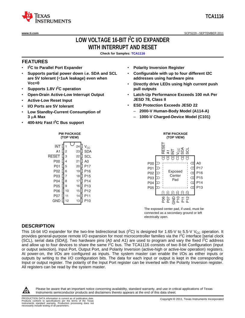
PW PACKAGE RTW PACKAGE(TOP VIEW) (TOP VIEW)
The exposed center pad, if used, must beconnected as a secondary ground or leftelectrically open.
DESCRIPTIONThis 16-bit I/O expander for the two-line bidirectional bus (I2C) is designed for 1.65-V to 5.5-V VCC operation. Itprovides general-purpose remote I/O expansion for most microcontroller families via the I2C interface [serial clock(SCL), serial data (SDA)]. Two hardware pins (A0 and A1) are used to program and vary the fixed I2C addressand allow up to four devices to share the same I2C bus. The TCA1116 consists of two 8-bit Configuration (inputor output selection), Input Port, Output Port, and Polarity Inversion (active-high or active-low operation) registers.At power-on, the I/Os are configured as inputs. The system master can enable the I/Os as either inputs oroutputs by writing to the I/O configuration bits. The data for each input or output is kept in the correspondingInput or output register. The polarity of the Input Port register can be inverted with the Polarity Inversion register.All registers can be read by the system master.
1
Please be aware that an important notice concerning availability, standard warranty, and use in critical applications of TexasInstruments semiconductor products and disclaimers thereto appears at the end of this data sheet.
This integrated circuit can be damaged by ESD. Texas Instruments recommends that all integrated circuits be handled withappropriate precautions. Failure to observe proper handling and installation procedures can cause damage.
ESD damage can range from subtle performance degradation to complete device failure. Precision integrated circuits may be moresusceptible to damage because very small parametric changes could cause the device not to meet its published specifications.
DESCRIPTION CONTINUEDThe system master can reset the TCA1116 in the event of a time-out or other improper operation by asserting alow in the RESET input. The power-on reset puts the registers in their default state and initializes the I2C/SMBusstate machine. Asserting RESET causes the same reset/initialization to occur without depowering the part.
The TCA1116 open-drain interrupt (INT) output is activated when any input state differs from its correspondingInput Port register state and is used to indicate to the system master that an input state has changed.
INT can be connected to the interrupt input of a microcontroller. By sending an interrupt signal on this line, theremote I/O can inform the microcontroller if there is incoming data on its ports without having to communicate viathe I2C bus. Thus, the TCA1116 can remain a simple slave device.
The device outputs (latched) have high-current drive capability for directly driving LEDs. The device has lowcurrent consumption.
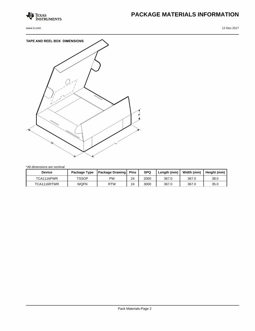
ORDERING INFORMATIONTA PACKAGE (1) (2) ORDERABLE PART NUMBER TOP-SIDE MARKING
TSSOP – PW Reel of 2000 TCA1116PWR RL116–40°C to 85°C
QFN – RTW Reel of 3000 TCA1116RTWR RL116
(1) Package drawings, thermal data, and symbolization are available at www.ti.com/packaging.(2) For the most current package and ordering information, see the Package Option Addendum at the end of this document, or see the TI
TCA1116PWR ACTIVE TSSOP PW 24 2000 Green (RoHS& no Sb/Br)
CU NIPDAU Level-1-260C-UNLIM -40 to 85 RL116
TCA1116RTWR ACTIVE WQFN RTW 24 3000 Green (RoHS& no Sb/Br)
CU NIPDAU Level-1-260C-UNLIM -40 to 85 RL116
(1) The marketing status values are defined as follows:ACTIVE: Product device recommended for new designs.LIFEBUY: TI has announced that the device will be discontinued, and a lifetime-buy period is in effect.NRND: Not recommended for new designs. Device is in production to support existing customers, but TI does not recommend using this part in a new design.PREVIEW: Device has been announced but is not in production. Samples may or may not be available.OBSOLETE: TI has discontinued the production of the device.
(2) RoHS: TI defines "RoHS" to mean semiconductor products that are compliant with the current EU RoHS requirements for all 10 RoHS substances, including the requirement that RoHS substancedo not exceed 0.1% by weight in homogeneous materials. Where designed to be soldered at high temperatures, "RoHS" products are suitable for use in specified lead-free processes. TI mayreference these types of products as "Pb-Free".RoHS Exempt: TI defines "RoHS Exempt" to mean products that contain lead but are compliant with EU RoHS pursuant to a specific EU RoHS exemption.Green: TI defines "Green" to mean the content of Chlorine (Cl) and Bromine (Br) based flame retardants meet JS709B low halogen requirements of <=1000ppm threshold. Antimony trioxide basedflame retardants must also meet the <=1000ppm threshold requirement.
(3) MSL, Peak Temp. - The Moisture Sensitivity Level rating according to the JEDEC industry standard classifications, and peak solder temperature.
(4) There may be additional marking, which relates to the logo, the lot trace code information, or the environmental category on the device.
(5) Multiple Device Markings will be inside parentheses. Only one Device Marking contained in parentheses and separated by a "~" will appear on a device. If a line is indented then it is a continuationof the previous line and the two combined represent the entire Device Marking for that device.
(6) Lead/Ball Finish - Orderable Devices may have multiple material finish options. Finish options are separated by a vertical ruled line. Lead/Ball Finish values may wrap to two lines if the finishvalue exceeds the maximum column width.
Important Information and Disclaimer:The information provided on this page represents TI's knowledge and belief as of the date that it is provided. TI bases its knowledge and belief on informationprovided by third parties, and makes no representation or warranty as to the accuracy of such information. Efforts are underway to better integrate information from third parties. TI has taken andcontinues to take reasonable steps to provide representative and accurate information but may not have conducted destructive testing or chemical analysis on incoming materials and chemicals.TI and TI suppliers consider certain information to be proprietary, and thus CAS numbers and other limited information may not be available for release.
In no event shall TI's liability arising out of such information exceed the total purchase price of the TI part(s) at issue in this document sold by TI to Customer on an annual basis.
1. All linear dimensions are in millimeters. Any dimensions in parenthesis are for reference only. Dimensioning and tolerancingper ASME Y14.5M.
2. This drawing is subject to change without notice.
PACKAGE OUTLINE
4219135/A 11/2016
www.ti.com
WQFN - 0.8 mm max height
PLASTIC QUAD FLATPACK-NO LEAD
RTW0024B
A
0.08 C
0.1 C A B0.05 C
B
SYMM
SYMM
4.13.9
4.13.9
PIN 1 INDEX AREA
0.8 MAX
0.050.00
C
SEATING PLANE
PIN 1 ID(OPTIONAL)
2X2.5
20X 0.5
2X 2.5
1
6
18
13
7 12
24 19
2.45±0.1
24X 0.340.24
24X 0.50.3
(0.2) TYP
25
EXPOSEDTHERMAL PAD
NOTES: (continued)
3. For more information, see Texas Instruments literature number SLUA271 (www.ti.com/lit/slua271) .
EXAMPLE BOARD LAYOUT
4219135/A 11/2016
www.ti.com
WQFN - 0.8 mm max height
RTW0024B
PLASTIC QUAD FLATPACK-NO LEAD
SYMM
SYMM
LAND PATTERN EXAMPLESCALE: 20X
( 2.45)
24X (0.6)
24X (0.24)1
6
7 12
13
18
1924
(3.8)
(0.97)
(3.8)
(0.97)
25
(R0.05) TYP
20X (0.5)
(Ø0.2) TYPVIA
0.07 MAXALL AROUND 0.07 MIN
ALL AROUNDMETAL
SOLDER MASKOPENING
SOLDER MASKOPENING
METAL UNDERSOLDER MASK
SOLDER MASK DETAILS
NON SOLDER MASKDEFINED
(PREFERRED)SOLDER MASK
DEFINED
NOTES: (continued)
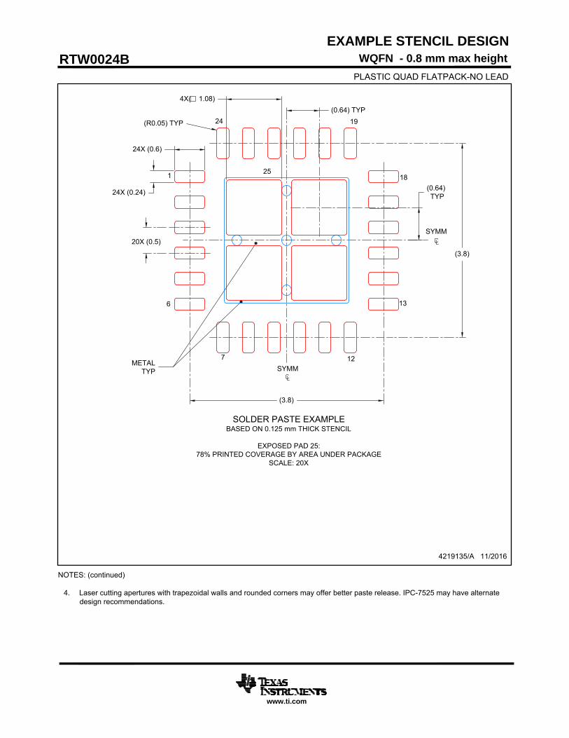
4. Laser cutting apertures with trapezoidal walls and rounded corners may offer better paste release. IPC-7525 may have alternatedesign recommendations.
EXAMPLE STENCIL DESIGN
4219135/A 11/2016
www.ti.com
WQFN - 0.8 mm max height
RTW0024B
PLASTIC QUAD FLATPACK-NO LEAD
SYMM
SYMM
SOLDER PASTE EXAMPLEBASED ON 0.125 mm THICK STENCIL
EXPOSED PAD 25:78% PRINTED COVERAGE BY AREA UNDER PACKAGE
SCALE: 20X
(3.8)
(0.64) TYP
1
6
7 12
13
18
1924
25
(0.64) TYP
4X( 1.08)
(R0.05) TYP
(3.8)
20X (0.5)
24X (0.24)
24X (0.6)
METALTYP
IMPORTANT NOTICE
Texas Instruments Incorporated (TI) reserves the right to make corrections, enhancements, improvements and other changes to itssemiconductor products and services per JESD46, latest issue, and to discontinue any product or service per JESD48, latest issue. Buyersshould obtain the latest relevant information before placing orders and should verify that such information is current and complete.TI’s published terms of sale for semiconductor products (http://www.ti.com/sc/docs/stdterms.htm) apply to the sale of packaged integratedcircuit products that TI has qualified and released to market. Additional terms may apply to the use or sale of other types of TI products andservices.Reproduction of significant portions of TI information in TI data sheets is permissible only if reproduction is without alteration and isaccompanied by all associated warranties, conditions, limitations, and notices. TI is not responsible or liable for such reproduceddocumentation. Information of third parties may be subject to additional restrictions. Resale of TI products or services with statementsdifferent from or beyond the parameters stated by TI for that product or service voids all express and any implied warranties for theassociated TI product or service and is an unfair and deceptive business practice. TI is not responsible or liable for any such statements.Buyers and others who are developing systems that incorporate TI products (collectively, “Designers”) understand and agree that Designersremain responsible for using their independent analysis, evaluation and judgment in designing their applications and that Designers havefull and exclusive responsibility to assure the safety of Designers' applications and compliance of their applications (and of all TI productsused in or for Designers’ applications) with all applicable regulations, laws and other applicable requirements. Designer represents that, withrespect to their applications, Designer has all the necessary expertise to create and implement safeguards that (1) anticipate dangerousconsequences of failures, (2) monitor failures and their consequences, and (3) lessen the likelihood of failures that might cause harm andtake appropriate actions. Designer agrees that prior to using or distributing any applications that include TI products, Designer willthoroughly test such applications and the functionality of such TI products as used in such applications.TI’s provision of technical, application or other design advice, quality characterization, reliability data or other services or information,including, but not limited to, reference designs and materials relating to evaluation modules, (collectively, “TI Resources”) are intended toassist designers who are developing applications that incorporate TI products; by downloading, accessing or using TI Resources in anyway, Designer (individually or, if Designer is acting on behalf of a company, Designer’s company) agrees to use any particular TI Resourcesolely for this purpose and subject to the terms of this Notice.TI’s provision of TI Resources does not expand or otherwise alter TI’s applicable published warranties or warranty disclaimers for TIproducts, and no additional obligations or liabilities arise from TI providing such TI Resources. TI reserves the right to make corrections,enhancements, improvements and other changes to its TI Resources. TI has not conducted any testing other than that specificallydescribed in the published documentation for a particular TI Resource.Designer is authorized to use, copy and modify any individual TI Resource only in connection with the development of applications thatinclude the TI product(s) identified in such TI Resource. NO OTHER LICENSE, EXPRESS OR IMPLIED, BY ESTOPPEL OR OTHERWISETO ANY OTHER TI INTELLECTUAL PROPERTY RIGHT, AND NO LICENSE TO ANY TECHNOLOGY OR INTELLECTUAL PROPERTYRIGHT OF TI OR ANY THIRD PARTY IS GRANTED HEREIN, including but not limited to any patent right, copyright, mask work right, orother intellectual property right relating to any combination, machine, or process in which TI products or services are used. Informationregarding or referencing third-party products or services does not constitute a license to use such products or services, or a warranty orendorsement thereof. Use of TI Resources may require a license from a third party under the patents or other intellectual property of thethird party, or a license from TI under the patents or other intellectual property of TI.TI RESOURCES ARE PROVIDED “AS IS” AND WITH ALL FAULTS. TI DISCLAIMS ALL OTHER WARRANTIES ORREPRESENTATIONS, EXPRESS OR IMPLIED, REGARDING RESOURCES OR USE THEREOF, INCLUDING BUT NOT LIMITED TOACCURACY OR COMPLETENESS, TITLE, ANY EPIDEMIC FAILURE WARRANTY AND ANY IMPLIED WARRANTIES OFMERCHANTABILITY, FITNESS FOR A PARTICULAR PURPOSE, AND NON-INFRINGEMENT OF ANY THIRD PARTY INTELLECTUALPROPERTY RIGHTS. TI SHALL NOT BE LIABLE FOR AND SHALL NOT DEFEND OR INDEMNIFY DESIGNER AGAINST ANY CLAIM,INCLUDING BUT NOT LIMITED TO ANY INFRINGEMENT CLAIM THAT RELATES TO OR IS BASED ON ANY COMBINATION OFPRODUCTS EVEN IF DESCRIBED IN TI RESOURCES OR OTHERWISE. IN NO EVENT SHALL TI BE LIABLE FOR ANY ACTUAL,DIRECT, SPECIAL, COLLATERAL, INDIRECT, PUNITIVE, INCIDENTAL, CONSEQUENTIAL OR EXEMPLARY DAMAGES INCONNECTION WITH OR ARISING OUT OF TI RESOURCES OR USE THEREOF, AND REGARDLESS OF WHETHER TI HAS BEENADVISED OF THE POSSIBILITY OF SUCH DAMAGES.Unless TI has explicitly designated an individual product as meeting the requirements of a particular industry standard (e.g., ISO/TS 16949and ISO 26262), TI is not responsible for any failure to meet such industry standard requirements.Where TI specifically promotes products as facilitating functional safety or as compliant with industry functional safety standards, suchproducts are intended to help enable customers to design and create their own applications that meet applicable functional safety standardsand requirements. Using products in an application does not by itself establish any safety features in the application. Designers mustensure compliance with safety-related requirements and standards applicable to their applications. Designer may not use any TI products inlife-critical medical equipment unless authorized officers of the parties have executed a special contract specifically governing such use.Life-critical medical equipment is medical equipment where failure of such equipment would cause serious bodily injury or death (e.g., lifesupport, pacemakers, defibrillators, heart pumps, neurostimulators, and implantables). Such equipment includes, without limitation, allmedical devices identified by the U.S. Food and Drug Administration as Class III devices and equivalent classifications outside the U.S.TI may expressly designate certain products as completing a particular qualification (e.g., Q100, Military Grade, or Enhanced Product).Designers agree that it has the necessary expertise to select the product with the appropriate qualification designation for their applicationsand that proper product selection is at Designers’ own risk. Designers are solely responsible for compliance with all legal and regulatoryrequirements in connection with such selection.Designer will fully indemnify TI and its representatives against any damages, costs, losses, and/or liabilities arising out of Designer’s non-compliance with the terms and provisions of this Notice.