111
SerialLite II IP Core User Guide Last updated for Quartus Prime Design Suite: 16.0 Subscribe Send Feedback UG-0705 2016.05.02 101 Innovation Drive San Jose, CA 95134 www.altera.com

SerialLite II IP Core User Guide
Last updated for Quartus Prime Design Suite: 16.0
Subscribe
Send Feedback
UG-07052016.05.02
101 Innovation DriveSan Jose, CA 95134www.altera.com
Contents
SerialLite II IP Core Overview............................................................................ 1-1General Description.....................................................................................................................................1-2Performance and Resource Utilization.....................................................................................................1-4
SerialLite II IP Core Getting Started.................................................................. 2-1Parameterize the IP Core............................................................................................................................ 2-1Set Up Simulation........................................................................................................................................ 2-3Generate Files............................................................................................................................................... 2-3Simulate the Design..................................................................................................................................... 2-4Instantiate the IP Core................................................................................................................................ 2-4Compile and Program................................................................................................................................. 2-4Specify Constraints...................................................................................................................................... 2-5
Assign Virtual Pins.......................................................................................................................... 2-5Fitter Constraints............................................................................................................................. 2-5Timing Constraints..........................................................................................................................2-5
SerialLite II Parameter Settings..................................................................................................................2-6Link Consistency............................................................................................................................2-12Data Rate......................................................................................................................................... 2-12Reference Clock Frequency.......................................................................................................... 2-13Port Type.........................................................................................................................................2-13Self Synchronized Link Up........................................................................................................... 2-16Scramble.......................................................................................................................................... 2-18Broadcast Mode..............................................................................................................................2-18Lane Polarity and Order Reversal................................................................................................2-19Data Type........................................................................................................................................ 2-20Packet Type.....................................................................................................................................2-20Flow Control Operation................................................................................................................2-23Transmit/Receive FIFO Buffers................................................................................................... 2-28Data Integrity Protection: CRC....................................................................................................2-30Transceiver Configuration............................................................................................................2-30Error Handling...............................................................................................................................2-33Optimizing the Implementation..................................................................................................2-34
SerialLite II IP Core Functional Description..................................................... 3-1Atlantic Interface..........................................................................................................................................3-2High-Speed Serial Interface........................................................................................................................ 3-4Clocks and Data Rates.................................................................................................................................3-4
Aggregate Bandwidth...................................................................................................................... 3-4External Clock Modes..................................................................................................................... 3-5Internal Clocking Configurations..................................................................................................3-6SerialLite II Deskew Support..........................................................................................................3-6
TOC-2
Altera Corporation
SerialLite II Clocking Structure......................................................................................................3-7SerialLite II Pin-Out Diagrams.................................................................................................... 3-13Initialization and Restart...............................................................................................................3-17
Multiple Core Configuration................................................................................................................... 3-18IP Core Configuration for Arria 10, Arria V, Cyclone V, and Stratix V Devices............................. 3-19
Design Consideration....................................................................................................................3-19Parameter Settings For SerialLite II and Custom PHY IP Cores............................................ 3-20Extra Signals Between SerialLite II and Custom PHY IP Cores..............................................3-22
SerialLite II Signals.................................................................................................................................... 3-23IP Core Verification...................................................................................................................................3-40
SerialLite II IP Core Testbench...........................................................................4-1Testbench Files............................................................................................................................................. 4-1Testbench Specifications.............................................................................................................................4-2Simulation Flow........................................................................................................................................... 4-7
Running a Simulation......................................................................................................................4-8Simulation Pass and Fail Conditions............................................................................................ 4-8
Testbench Components............................................................................................................................ 4-10AGEN.............................................................................................................................................. 4-11AMON.............................................................................................................................................4-13Status Monitors.............................................................................................................................. 4-17Clock and Reset Generator...........................................................................................................4-18Custom PHY IP Core.................................................................................................................... 4-18Example Testbench – Verilog HDL............................................................................................ 4-18
SerialLite II IP Core User Guide Archives......................................................... A-1
Revision History for SerialLite II IP Core User Guide...................................... B-1
TOC-3
Altera Corporation
SerialLite II IP Core Overview 12016.05.02
UG-0705 Subscribe Send Feedback
The SerialLite II MegaCore function is a lightweight protocol suitable for packet and streaming data inchip-to-chip, board-to-board, and backplane applications.
The SerialLite II protocol offers low gate count and minimum data transfer latency. It provides reliable,high-speed transfers of packets between devices over serial links. The protocol defines packet encapsula‐tion at the link layer and data encoding at the physical layer, and integrates transparently with existingnetworks without software support.
Table 1-1: SerialLite II IP Core Release Information
Information Description
Version 16.0
Release Date May 2016
Ordering Code IP-SLITE2
Device Family Support Arria® 10, Arria V, Arria II GX, Cyclone V, Stratix® V and Stratix IVdevice families.
Note: Arria 10 devices are indirectly supported by the SerialLite IIIP core version 15.0 and later. If your design needs toimplement SerialLite II interface in Arria 10 devices, contactyour local Altera representative or file a Service Request(SR) to obtain a design example, a guideline document, anda special license to enable the Quartus Prime software togenerate the FPGA configuration file (.sof) for the Arria 10devices.
Altera verifies that the current version of the Quartus Prime software compiles the previous version ofeach IP core. The IP Core Release Notes and Errata report any exceptions to this verification. Altera doesnot verify compilation with IP core versions older than one release.
© 2016 Altera Corporation. All rights reserved. ALTERA, ARRIA, CYCLONE, ENPIRION, MAX, MEGACORE, NIOS, QUARTUS and STRATIX words and logos aretrademarks of Altera Corporation and registered in the U.S. Patent and Trademark Office and in other countries. All other words and logos identified astrademarks or service marks are the property of their respective holders as described at www.altera.com/common/legal.html. Altera warrants performanceof its semiconductor products to current specifications in accordance with Altera's standard warranty, but reserves the right to make changes to anyproducts and services at any time without notice. Altera assumes no responsibility or liability arising out of the application or use of any information,product, or service described herein except as expressly agreed to in writing by Altera. Altera customers are advised to obtain the latest version of devicespecifications before relying on any published information and before placing orders for products or services.
ISO9001:2008Registered
www.altera.com101 Innovation Drive, San Jose, CA 95134

Table 1-2: SerialLite II IP Core Features
Features Description
Physical layer features • 622 Mbps to 6.375 Gbps per lane(1)
• Single or multiple lane support (up to 16 lanes)• 8-, 16-, or 32-bit data path per lane• Symmetric, asymmetric, unidirectional/simplex or broadcast mode• Optional payload scrambling• Full-duplex or self-synchronizing link state machine (LSM)• Channel bonding scalable up to 16 lanes• Synchronous or asynchronous operation• Automatic clock rate compensation for asynchronous use: ±100 and
±300 parts per million (ppm)
Link layer features • Atlantic interface compliant• Support for two user packet types: data packet and priority packet• Optional packet integrity protection using cyclic redundancy code
(CRC-32 or CRC-16)• Optional link management packets
• Retry-on-error for priority packets• Individual port (data/priority) flow control
• Unrestricted data and priority packet size• Support for TimeQuest timing analyzer• Polarity reversal• Lane order reversal• IP functional simulation models for use in Altera-supported VHDL
and Verilog HDL simulators
Related InformationSerialLite II IP Core User Guide Archives on page 5-1Provides a list of user guides for previous versions of the SerialLite II IP core.
General DescriptionThe SerialLite II IP core is a simple, high-speed, low-latency, and low-resource point-to-point serial datacommunication link.
The SerialLite II IP core performs up to:
• 3.75 Gbps in Arria II GX devices• 5 Gbps in Cyclone V devices• 6.375 Gbps in Arria V, Stratix IV, and Stratix V devices• More than 6.375 Gbps in Arria 10 devices
(1) For Arria 10 devices, the IP core supports higher than 6.375 Gbps per lane.
1-2 General DescriptionUG-0705
2016.05.02
Altera Corporation SerialLite II IP Core Overview
Send Feedback
The SerialLite II IP core is highly configurable, and provides a wide range of functionality suited tomoving data in many different environments.
The IP core provides a simple and lightweight way to move data from one point to another reliably at highspeeds. It consists of a serial link of up to 16 bonded lanes, with logic to provide a number of basic andoptional link support functions. The Atlantic interface is the primary access for delivering and receivingdata.
The SerialLite II protocol specifies a link that is simple to build, uses as little logic as possible, and requireslittle work for a logic designer to implement. The SerialLite II MegaCore function uses all of the featuresavailable in the SerialLite II protocol. You can parameterize the IP core using the SerialLite II parametereditor.
A link built using the SerialLite II IP core operates at 622 Mbps to 6.375 Gbps per lane (or more for Arria10 devices). Link reliability is enhanced by the 8B10B encoding scheme and optional CRC capabilities.You can achieve further reductions in the bit-error rate by using the optional retry-on-error feature. Datarate and consumption mismatches can be accommodated using the optional flow-control feature toensure that no data is lost.
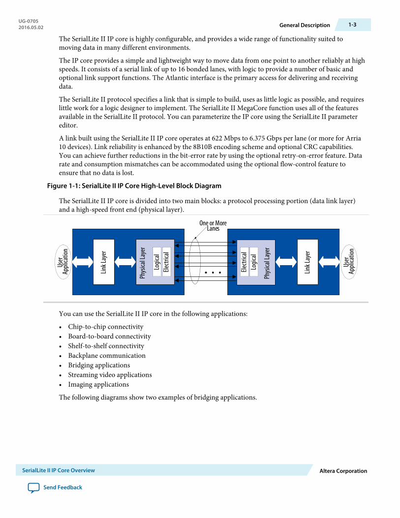
Figure 1-1: SerialLite II IP Core High-Level Block Diagram
The SerialLite II IP core is divided into two main blocks: a protocol processing portion (data link layer)and a high-speed front end (physical layer).
One or MoreLanes
Logic
alEle
ctrica
l
Phys
ical L
ayer
Link L
ayer
Logic
alEle
ctrica
l
Phys
ical L
ayer
Link L
ayer
User
Appli
catio
n
User
Appli
catio
n
You can use the SerialLite II IP core in the following applications:
• Chip-to-chip connectivity• Board-to-board connectivity• Shelf-to-shelf connectivity• Backplane communication• Bridging applications• Streaming video applications• Imaging applications
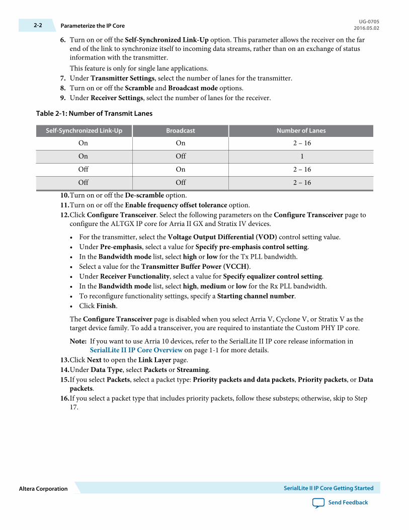
The following diagrams show two examples of bridging applications.
UG-07052016.05.02 General Description 1-3
SerialLite II IP Core Overview Altera Corporation
Send Feedback
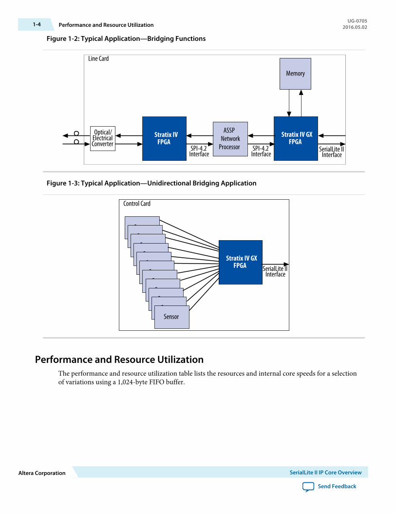
Figure 1-2: Typical Application—Bridging Functions
Memory
ASSPNetwork
Processor
Stratix IV GXFPGA
Stratix IVFPGA
SPI-4.2Interface
SPI-4.2Interface
SerialLite IIInterface
Optical/ElectricalConverter
Line Card
Figure 1-3: Typical Application—Unidirectional Bridging Application
Stratix IV GXFPGA SerialLite II
Interface
Control Card
SensorSensor
SensorSensor
SensorSensor
SensorSensor
SensorSensor
Sensor
Performance and Resource UtilizationThe performance and resource utilization table lists the resources and internal core speeds for a selectionof variations using a 1,024-byte FIFO buffer.
1-4 Performance and Resource UtilizationUG-0705
2016.05.02
Altera Corporation SerialLite II IP Core Overview
Send Feedback

Table 1-3: Performance for Stratix IV Devices
These results were obtained using the Quartus Prime software version 16.0 for the Stratix IV device(EP4SGX70HF35C2).
Lane PacketType
TransferSize
CRC ROE FC Through-put atMbps
RXBuffer
Size(Data)
RXBuffer
Size(Prio)
Combina‐tionalALUT
Memory9K
MemoryALUT
LogicRegister
1 Data 1 0 0 0 1250 – – 841 10 18 856
1 Data 2 0 0 0 3125 – – 847 11 0 820
1 Data 4 0 0 0 6375 – – 935 21 20 959
4 Data 1 0 0 0 1250 – – 1399 21 56 1291
4 Data 2 0 0 0 3125 – – 1636 31 112 1507
4 Data 4 0 0 0 6375 – – 2184 50 0 1748
16 Data 2 0 0 0 3125 – – 4416 87 308 3656
16 Data 4 0 0 0 6375 – – 6685 181 0 5066
1 Data 1 32 0 1 1250 1024 – 1135 11 35 1265
1 Data 2 32 0 1 3125 1024 – 1189 12 16 1206
1 Data 4 32 0 1 6375 2048 – 1413 22 36 1357
4 Data 1 32 0 1 1250 2048 – 1814 22 72 1675
4 Data 2 32 0 1 3125 4096 – 2380 32 128 1995
4 Data 4 32 0 1 6375 8192 – 3402 51 16 2326
1 Priority 2 16 1 1 3125 – 1024 1519 21 16 1396
1 Priority 4 16 1 1 6375 – 2048 1745 32 36 1541
4 Priority 2 16 1 1 3125 – 4096 2687 51 128 2165
4 Priority 4 16 1 1 6375 – 8192 3661 71 488 3626
Table 1-4: Fmax for Stratix IV Devices
The performance results were obtained using these frequencies at 900 mV 85°C Corner.
Lane Packet Type Transfer Size Fmax(txrdp_clk)
MHz
Fmax(rxrdp_clk)
MHz
Fmax(txhpp_clk)
MHz
Fmax (rxhpp_clk)
MHz
1 Data 1 252.78 261.3 – –
1 Data 2 294.38 302.57 – –
1 Data 4 292.06 298.06 – –
UG-07052016.05.02 Performance and Resource Utilization 1-5
SerialLite II IP Core Overview Altera Corporation
Send Feedback

Lane Packet Type Transfer Size Fmax(txrdp_clk)
MHz
Fmax(rxrdp_clk)
MHz
Fmax(txhpp_clk)
MHz
Fmax (rxhpp_clk)
MHz
4 Data 1 287.77 286.62 – –
4 Data 2 285.47 299.94 – –
4 Data 4 325.31 292.91 – –
16 Data 2 312.99 285.8 – –
16 Data 4 260.35 247.52 – –
1 Data 1 258.67 274.73 – –
1 Data 2 281.61 256.02 – –
1 Data 4 282.97 274.35 – –
4 Data 1 291.12 271.67 – –
4 Data 2 269.61 264.97 – –
4 Data 4 271.67 267.02 – –
1 Priority 2 – – 287.69 252.33
1 Priority 4 – – 271.59 283.77
4 Priority 2 – – 259.61 288.1
4 Priority 4 – – 337.5 272.33
1-6 Performance and Resource UtilizationUG-0705
2016.05.02
Altera Corporation SerialLite II IP Core Overview
Send Feedback

SerialLite II IP Core Getting Started 22016.05.02
UG-0705 Subscribe Send Feedback
The SerialLite II IP core is installed as part of the Quartus® Prime installation process.
You can select and parameterize any Altera IP core from the library. Altera provides an integratedparameter editor that allows you to customize the SerialLite II IP core to support a wide variety of applica‐tions.
Related Information
• Introduction to Altera IP CoresProvides general information about all Altera IP cores, including parameterizing, generating,upgrading, and simulating IP.
• Creating Version-Independent IP and Qsys Simulation ScriptsCreate simulation scripts that do not require manual updates for software or IP version upgrades.
• Project Management Best PracticesGuidelines for efficient management and portability of your project and IP files.
Parameterize the IP CoreThe SerialLite II IP core parameter editor guides you through the setting of parameter values and selectionof optional ports.
1. Click Parameter Settings in the SerialLite II parameter editor. The Physical Layer page appears.2. Key in a data rate in megabits per second (Mbps). The SerialLite II IP core supports data rates of 622 to
6,375 Mbps per lane.
Note: For Arria 10 devices, the IP core supports higher than 6.375 Gbps per lane.3. Choose a Transfer size. The Transfer size determines the number of contiguous data columns. The
Transfer size also determines the serialization/deserialization (SERDES) factor and internal data pathwidth.
4. Specify the Reference Clock Frequency. This option defines the frequency of the reference clock forthe Arria II GX or Stratix IV internal transceiver. You can select any frequency supported by thetransceiver.This option is not available in Arria V, Cyclone V, and Stratix V configurations.
5. Select a Port Type. You have three choices: Bidirectional, Transmitter only, and Receiver only.If you choose Transmitter only or Receiver only, the Self-Synchronized Link-Up parameter (LSM) isenabled by default.
© 2016 Altera Corporation. All rights reserved. ALTERA, ARRIA, CYCLONE, ENPIRION, MAX, MEGACORE, NIOS, QUARTUS and STRATIX words and logos aretrademarks of Altera Corporation and registered in the U.S. Patent and Trademark Office and in other countries. All other words and logos identified astrademarks or service marks are the property of their respective holders as described at www.altera.com/common/legal.html. Altera warrants performanceof its semiconductor products to current specifications in accordance with Altera's standard warranty, but reserves the right to make changes to anyproducts and services at any time without notice. Altera assumes no responsibility or liability arising out of the application or use of any information,product, or service described herein except as expressly agreed to in writing by Altera. Altera customers are advised to obtain the latest version of devicespecifications before relying on any published information and before placing orders for products or services.
ISO9001:2008Registered
www.altera.com101 Innovation Drive, San Jose, CA 95134
6. Turn on or off the Self-Synchronized Link-Up option. This parameter allows the receiver on the farend of the link to synchronize itself to incoming data streams, rather than on an exchange of statusinformation with the transmitter.This feature is only for single lane applications.
7. Under Transmitter Settings, select the number of lanes for the transmitter.8. Turn on or off the Scramble and Broadcast mode options.9. Under Receiver Settings, select the number of lanes for the receiver.
Table 2-1: Number of Transmit Lanes
Self-Synchronized Link-Up Broadcast Number of Lanes
On On 2 – 16
On Off 1
Off On 2 – 16
Off Off 2 – 16
10.Turn on or off the De-scramble option.11.Turn on or off the Enable frequency offset tolerance option.12.Click Configure Transceiver. Select the following parameters on the Configure Transceiver page to
configure the ALTGX IP core for Arria II GX and Stratix IV devices.
• For the transmitter, select the Voltage Output Differential (VOD) control setting value.• Under Pre-emphasis, select a value for Specify pre-emphasis control setting.• In the Bandwidth mode list, select high or low for the Tx PLL bandwidth.• Select a value for the Transmitter Buffer Power (VCCH).• Under Receiver Functionality, select a value for Specify equalizer control setting.• In the Bandwidth mode list, select high, medium or low for the Rx PLL bandwidth.• To reconfigure functionality settings, specify a Starting channel number.• Click Finish.
The Configure Transceiver page is disabled when you select Arria V, Cyclone V, or Stratix V as thetarget device family. To add a transceiver, you are required to instantiate the Custom PHY IP core.
Note: If you want to use Arria 10 devices, refer to the SerialLite II IP core release information in SerialLite II IP Core Overview on page 1-1 for more details.
13.Click Next to open the Link Layer page.14.Under Data Type, select Packets or Streaming.15.If you select Packets, select a packet type: Priority packets and data packets, Priority packets, or Data
packets.16.If you select a packet type that includes priority packets, follow these substeps; otherwise, skip to Step
17.
2-2 Parameterize the IP CoreUG-0705
2016.05.02
Altera Corporation SerialLite II IP Core Getting Started
Send Feedback
• Turn on or off the Retry-on-error option.• If you turned on Retry-on-error, specify a value for Timeout and Segment size.• Under Buffer Size, specify a value for Transmitter and Receiver.• Turn on or off the Enable flow control option.• If you turned on Enable flow control, specify the values for Pause quantum time, Threshold, and
Refresh period.• If you selected Priority packets only, skip Step 17.
17.If you selected a packet type that includes data packets, follow these substeps;
• Turn on or off the Enable flow control option.• If you turned on Enable flow control, specify the values for Pause quantum time, Threshold, and
Refresh period.• Under Buffer Size, specify a value for Transmitter and Receiver.
18.If your transmitter or receiver requires cyclic redundancy code (CRC) checking, turn on the EnableCRC option for your chosen packet type and specify a value for CRC Type.
Related InformationSerialLite II Parameter Settings on page 2-6
Set Up SimulationAn IP functional simulation model is a cycle-accurate VHDL or Verilog HDL model produced by theQuartus Prime software. The model allows for fast functional simulation of IP using industry-standardVHDL and Verilog HDL simulators.
To generate an IP functional simulation model for your IP core:
1. On the EDA page, under Simulation Libraries, turn on Generate Simulation Model.2. Some third-party synthesis tools can use a netlist that contains only the structure of the IP core, but
not detailed logic, to optimize performance of the design that contains the IP core. If your synthesistool supports this feature, turn on Generate netlist.
3. Click Next to display the Summary page.
Note: For Arria V, Cyclone V, and Stratix V devices, the generated simulation model does not comewith transceiver. You need to integrate yourself. When you generate the transceiver, alsoinclude the reset controller for the respective devices. For Arria 10 devices, contact your localAltera representative or file a Service Request (SR).
Generate FilesYou can use the check boxes on the Summary page to enable or disable the generation of specified files. Agray checkmark indicates a file that is automatically generated; other checkmarks indicate optional files.
UG-07052016.05.02 Set Up Simulation 2-3
SerialLite II IP Core Getting Started Altera Corporation
Send Feedback
To generate your parameterized IP core:
1. Turn on the files you want to generate.2. To generate the specified files and close the SerialLite II parameter editor, click Finish. The generation
phase can take several minutes to complete.3. If you generate the IP core instance in a Quartus Prime project, you are prompted to add the Quartus
Prime IP File (.qip) to the current Quartus Prime project.The .qip file is generated by the SerialLite II parameter editor and contains information about agenerated IP core. In most cases, the .qip file contains all of the necessary assignments and informationrequired to process the IP core or system in the Quartus Prime compiler. The SerialLite II parametereditor generates a single .qip file for each IP core.
Note: For Arria V, Cyclone V, and Stratix V devices, you must also generate the Custom PHY andreset controller, and then add the transceiver .qip files in. You must manually integrate thetransceiver to the SerialLite II IP core, and the reset controller to the transceiver. For Arria 10devices, contact your local Altera representative or file a Service Request (SR).
4. After your review the generation report, <variation name>.html, in your project directory, click Exit toclose the SerialLite II parameter editor.
Simulate the DesignYou can simulate your design using the Quartus-generated VHDL and Verilog HDL IP functionalsimulation models.
Altera also provides a Verilog HDL demonstration testbench that shows you how to instantiate a model ina design for all configurations. Altera also provides a VHDL demonstration testbench for a restrictednumber of configurations. The testbench stimulates the inputs and checks the outputs of the interfaces ofthe SerialLite II IP core, allowing you to evaluate the IP core’s basic functionality.
Note: For Arria V, Cyclone V, and Stratix V devices, the generated testbench is incorrect because the toplevel design has the transceiver integrated with it. The generated simulation model does not havethe transceiver integrated with it, so you need to change the testbench accordingly. For thesedevices, you also need to modify the generated simulation script to add the Custom PHYtransceiver files. For Arria 10 devices, contact your local Altera representative or file a ServiceRequest (SR).
Related InformationSerialLite II IP Core Testbench on page 4-1
Instantiate the IP CoreYou can now integrate your custom IP core variation into your design and simulate your complete designusing your own custom testbench.
Compile and ProgramAfter you are done with simulating and instantiating the IP core, you can compile and program yourdesign
2-4 Simulate the DesignUG-0705
2016.05.02
Altera Corporation SerialLite II IP Core Getting Started
Send Feedback

1. Click Start Compilation on the Processing menu in the Quartus Prime software to compile yourdesign.
2. After successfully compiling your design, program the targeted Altera device with the Programmer inthe Tools menu and verify the design in hardware.
Specify ConstraintsThe SerialLite II example design applies constraints to create virtual pins and set up timing analysis.
Assign Virtual PinsIf you are compiling the SerialLite II IP core variation as a standalone component, you must specifyvirtual pin assignments. The SerialLite II parameter editor generates a tool command language (Tcl) scriptthat automates this task.
To run the script:
1. On the Tools menu, click Tcl Scripts to open the Tcl Scripts dialog box.2. In the project directory, select <variation_name>_constraints.3. Click Run.
Note: The script assumes the default names for the virtual pins. If you have connected the pins tonames other than the default names, you must edit this script and change the virtual pin nameswhen the core is still compiled in stand-alone mode.
Fitter ConstraintsThe Tcl script also optimizes fitter settings to produce the best performance (fMAX). Use this script as aguide to set constraints for the SerialLite II IP core variation in your design. The timing constraints arecurrently set for the SerialLite II IP core variation as a standalone component, so you must update thescript with hierarchy information for your own design. The Tcl script also points to the generatedSynopsys Design Constraints (SDC) timing constraint script if the TimeQuest timing analyzer is enabled.
The The Fitter optimizes your design based on the requirements in the .sdc files in your project. Thescript uses the FITTER_EFFORT "STANDARD FIT" Fitter setting.
Note: This fitter setting may conflict with your Quartus Prime software settings.
You can now integrate your IP core variation into your design and simulate and compile.
Timing ConstraintsThe SerialLite II IP core generates an ASCII file (with the .sdc extension) that contains design constraintsand timing assignments in the industry-standard SDC format. The constraints in the .sdc file aredescribed using the Tcl tool command language and follow Tcl syntax rules.
To specify the TimeQuest timing analyzer as the default timing analyzer:
1. On the Assignments menu, click Timing Analysis Settings.2. In the Timing Analysis Settings page, turn on Use TimeQuest Timing Analyzer during compila‐
tion.The TimeQuest timing constraints are currently set for the SerialLite II IP core variation as astandalone component. You must update the script with hierarchy information if your own design isnot a standalone component.
UG-07052016.05.02 Specify Constraints 2-5
SerialLite II IP Core Getting Started Altera Corporation
Send Feedback

Note: The .sdc generated for an Arria V, Cyclone V, or Stratix V device is incomplete. You need tochange the "set_clock_groups" assignment which specifies "<variant_name>*receive|clkout" and "<variant_nane>*transmit|clkout" to the correct name of the clkout signalscoming from the transceiver. Other similar clocks from the transceiver in the generated .sdc arealso incorrect and need to be replaced by the actual name and path accordingly. For Arria 10devices, contact your local Altera representative or file a Service Request (SR).
SerialLite II Parameter SettingsYou set the parameters using the SerialLite II parameter editor.
Table 2-2: SerialLite II Parameters
Parameter Description
Physical Layer
Device family Select the targeted device family.
Note: For Arria 10 devices, contact your local Altera representa‐tive or file a Service Request (SR).
Data rate Key in a data rate in megabits per second (Mbps). The SerialLite II IPcore supports data rates of 622 to 6,375 Mbps per lane.
Note: The data rate must be an acceptable range for the Transfersize. The parameter editor returns a warning or an errormessage if you specify a data rate that is not within therange for the specified Transfer size.
Transfer size The Transfer size (TSIZE) parameter determines the number ofcontiguous data columns and the internal data path width per lane.
• TSIZE 1— equates to an internal data path of 8 bits (Recommendedfor less than 2.5 gigabits per second (Gbps))
• TSIZE 2 —equates to an internal data path of 16 bits(Recommended for less than or equal to 3.125 Gbps)
• TSIZE 4 —equates to an internal data path of 32 bits (Typically forgreater than 3.125 Gbps, and only available for Arria V, Cyclone V,Stratix IV, and Stratix V devices)
A transfer size also determines the width of the SERDES block:
• TSIZE 1—10 bit-wide SERDES block• TSIZE 2—20 bit-wide SERDES block• TSIZE 4—40 bit-wide SERDES block
2-6 SerialLite II Parameter SettingsUG-0705
2016.05.02
Altera Corporation SerialLite II IP Core Getting Started
Send Feedback
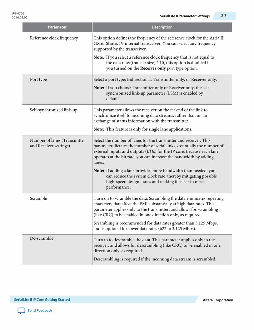
Parameter Description
Reference clock frequency This option defines the frequency of the reference clock for the Arria IIGX or Stratix IV internal transceiver. You can select any frequencysupported by the transceiver.
Note: If you select a reference clock frequency that is not equal tothe data rate/(transfer size) * 10, this option is disabled ifyou turned on the Receiver only port type option.
Port type Select a port type: Bidirectional, Transmitter only, or Receiver only.
Note: If you choose Transmitter only or Receiver only, the self-synchronized link-up parameter (LSM) is enabled bydefault.
Self-synchronized link-up This parameter allows the receiver on the far end of the link tosynchronize itself to incoming data streams, rather than on anexchange of status information with the transmitter.
Note: This feature is only for single lane applications.
Number of lanes (Transmitterand Receiver settings)
Select the number of lanes for the transmitter and receiver. Thisparameter dictates the number of serial links, essentially the number ofexternal inputs and outputs (I/Os) for the IP core. Because each laneoperates at the bit rate, you can increase the bandwidth by addinglanes.
Note: If adding a lane provides more bandwidth than needed, youcan reduce the system clock rate, thereby mitigating possiblehigh-speed design issues and making it easier to meetperformance.
Scramble Turn on to scramble the data. Scrambling the data eliminates repeatingcharacters that affect the EMI substantially at high data rates. Thisparameter applies only to the transmitter, and allows for scrambling(like CRC) to be enabled in one direction only, as required.
Scrambling is recommended for data rates greater than 3,125 Mbps,and is optional for lower data rates (622 to 3,125 Mbps).
De-scramble Turn to to descramble the data. This parameter applies only to thereceiver, and allows for descrambling (like CRC) to be enabled in onedirection only, as required.
Descrambling is required if the incoming data stream is scrambled.
UG-07052016.05.02 SerialLite II Parameter Settings 2-7
SerialLite II IP Core Getting Started Altera Corporation
Send Feedback

Parameter Description
Broadcast mode Turn on to use broadcast mode. This parameter applies only to thetransmitter.
If you enable this parameter, you configure the IP core to use a singleshared transmitter and multiple receivers in the master device.
Enable frequency offset tolerance This parameter sets the value for the frequency offset tolerance (clockcompensation). This parameter also determines whether the system isconfigured for synchronous or asynchronous clocking operation.
If you turn on this option, select an offset tolerance of ±100 or ±300parts per million (ppm).
Link Layer
Data type Select whether to format the data as a stream or in packets. If you selectStreaming, all link layer basic parameters, including data and priorityports, and buffering are disabled (grayed out). Streaming mode doesnot include link-layer functions.
Packet type Select whether to send your packets as priority packets, data packets, orboth.
Enable flow control The SerialLite II IP core provides this parameter as an optional meansof exerting backpressure on a data source when data consumption istoo slow. Turn on this parameter to ensure that the receive FIFObuffers do not overflow.
Note: Flow control is only needed when the system logic on thereceiving end of the link is reading the data slower than thesystem logic on the transmitting end of the link is sendingdata.
Pause quantum time Activation of flow control causes a pause in transmission. Specify apause duration from to 8 to 2,040 columns.
Threshold You must set the Threshold parameter to a value such that the FIFOdoes not completely empty during a flow control operation (this cancause inefficiencies in the system), and leave enough room in the FIFOto ensure any remaining data in the system can be safely stored in theFIFO without the FIFO overflowing
Refresh period The flow control refresh period determines the number of columnsbefore a flow control packet can be retransmitted (for example if a flowcontrol link management packet is lost or corrupted). This period mustbe less than the pause quantum time. The packet is retransmitted if theFIFO buffer is still breached.
2-8 SerialLite II Parameter SettingsUG-0705
2016.05.02
Altera Corporation SerialLite II IP Core Getting Started
Send Feedback

Parameter Description
Retry-on-error This parameter improves the bit error rate of your data.
• On: Logic is created to acknowledge segments and retransmitsegments when errors occur. Eight transmit segment buffers arecreated.
• Off: Logic is not created to acknowledge segments. This is thedefault setting.
If you turn off this parameter, no segment acknowledgments aregenerated or expected, and all segments are transmitted without anyacknowledgments from the receiver.
This parameter is only available for priority packets.
Timeout Set the time out value for the segment to be acknowledged. The time-out value is based primarily on the round trip latency—from the time apacket is sent to when the acknowledge signal is returned to thattransmitter. The exact value of the round trip latency is undetermined,pending device characterization, but a value of 1,024 columns isrecommended.
• Do not to set the time out to be too long so the system does nothave to wait too long for link errors to resolve.
• Do not set the time out to be too short because then the systemalways times out and the link never remains up.
Segment size This parameter is only applicable when the Retry-on-error parameteris turned on. This parameter settings range from 8 to 2,048 bytes in 2n
increments, and the default value is 256 bytes.
Priority packets are broken into segments of segment size bytes andsent across the link. Priority packets less than or equal to segment sizebytes and without an end marker are buffered before transmission.This buffering is required to support the Retry-on-error option, whichis only allowed for priority packets.
If a packet is larger than a segment size, a full segment must be queuedbefore it can be transmitted. This queuing may result in mid-packetbackpressure on the priority port Atlantic interface. Segmentinterleaving, priority segments destined for different ports, is fullysupported, as long as the address change occurs on a segmentboundary.
Buffer size (Transmitter andReceiver)
Specify a FIFO buffer size value for the transmitter and receiver.
UG-07052016.05.02 SerialLite II Parameter Settings 2-9
SerialLite II IP Core Getting Started Altera Corporation
Send Feedback

Parameter Description
Enable CRC for priority/datapackets (Transmitter andReceiver)
If your transmitter or receiver requires cyclic redundancy code (CRC)checking, turn on the Enable CRC option for your chosen packet type.
• On: CRC logic is created. CRC usage is specified independently foreach port.
• Off: CRC logic is not created. CRC usage is specified independentlyfor each port. This is the default CRC setting.
CRC Type Select 16 bits or 32 bits for the CRC type.
• 16 bits: Generates a two-byte CRC. Adequate for packets of around1 KBytes or smaller. This is the default algorithm when CRC isenabled.
• 32 bits: Generates a 4-byte CRC. Should only be used for packetslarger than about 1 KBytes or when extreme protection is required,because it is resource-intensive.
Configure Transceiver (only applicable for Arria II GX and Stratix IV devices)
Specify VOD control setting Select the Voltage Output Differential (VOD) control setting value.
Note: This parameter is disabled when the number of lanes in thetransmit direction is equal to zero.
Specify pre-emphasis controlsetting
Select pre-emphasis control setting value.
For Stratix IV devices, the pre-emphasis control values supported are0,1,2,3,4, and 5.
• 0 = Pre-emphasis option is turned off• 1 = Maximum negative value• 2 = Medium negative value• 3 = Special value in which only the first post-tap is set (set to the
maximum), while the other taps are off• 4 = Medium positive value• 5 = Maximum positive value
For Arria II GX devices, the pre-emphasis setting cannot be changed.
This parameter is set to 0 by default. It is disabled when the number oflanes in the transmit direction is equal to zero.
2-10 SerialLite II Parameter SettingsUG-0705
2016.05.02
Altera Corporation SerialLite II IP Core Getting Started
Send Feedback
Parameter Description
Bandwidth mode (Transmitterand Receiver)
The transmitter and receiver PLLs in the ALTGX IP core offerprogrammable bandwidth settings. The PLL bandwidth is the measureof its ability to track the input clock and jitter, determined by the -3 dBfrequency of the PLL’s closed-loop gain.
Select low or high bandwidth mode for the transmitter and low,medium, or high bandwidth mode for the receiver.
• The low bandwidth setting filters out more high frequency inputclock jitter, but increases lock time. The PLL is set to the low settingby default.
• The medium setting balances the lock time and noise rejection/jitter filtering between the high and low settings.
• The high bandwidth setting provides a faster lock time and tracksmore jitter on the input clock source which passes it through thePLL to help reject noise from the voltage control oscillator (VCO)and power supplies.
If the number of lanes in the transmit or receive direction is equal tozero, the bandwidth mode for that direction is disabled.
Note: This parameter is not applicable for Arria II GX devices.
Transmitter buffer power(VCCH)
This setting is used to calculate the VOD from the buffer power supplyand the transmitter termination to derive the proper VOD range.
• Arria II GX devices = 1.5 V• Stratix IV devices = 1.4 V or 1.5 V
Specify equalizer control setting Select the equalizer control setting value.
The transceiver offers an equalization circuit in each receiver channelto increase noise margins and help reduce the effects of high frequencylosses. The programmable equalizer compensates for inter-symbolinterference (ISI) and high frequency losses that distort the signal andreduce the noise margin of the transmission medium by equalizing thefrequency response.
For Stratix IV devices, the equalization control values supported are 0,1, 2, 3, and 4. These values correspond to lowest/off (0), betweenmedium and lowest (1), medium (2), between medium and high (3),and high (4).
For Arria II GX devices, the equalization cannot be changed.
UG-07052016.05.02 SerialLite II Parameter Settings 2-11
SerialLite II IP Core Getting Started Altera Corporation
Send Feedback

Parameter Description
Starting channel number To reconfigure the functionality settings, select a starting channelnumber. The range for the dynamic reconfiguration starting channelnumber setting is 0 to 380. These ranges are in multiples of fourbecause the dynamic reconfiguration interface is per transceiver block.The range 0 to 380 is the logical channel address, based purely on thenumber of possible transceiver instances.
Note: This parameter is not applicable for Arria II GX devices.
Related InformationParameterize the IP Core on page 2-1
Link ConsistencyA SerialLite II link consists of two instantiations of logic implementing the SerialLite II protocol.
Each end of the link has a transmitter and a receiver.
Figure 2-1: Complete SerialLite II Link
FPGA 2
SerialLite II System
FPGA 1
SerialLite IIMegaCore
SystemLogic Logic
One ormore lanes
Tx
Rx
Rx
Tx
Atlantic InterfaceAtlantic Interface
High-SpeedTransceivers
High-SpeedTransceivers
FunctionVariation
MegaCoreFunctionVariation
Data RateThe data rate range varies based on the device and the transfer size (TSIZE).
The SerialLite II IP core supports a data rate range of 622 to 6,375 Mbps per lane. In Arria II GX devices,the data rate must be less than 3,750 Mbps, and in Stratix IV devices, less than 6,375 Mbps.
2-12 Link ConsistencyUG-0705
2016.05.02
Altera Corporation SerialLite II IP Core Getting Started
Send Feedback

Table 2-3: Data Rate Dependencies on Transfer Size
DevicesData Rate
2.5 Gbps 3.125 Gbps 3.75 Gbps 5 Gbps 6.375 Gbps
Arria II GX TSIZE= 1, 2 TSIZE= 2 TSIZE= 2 Not Supported Not Supported
Stratix IVGX
TSIZE= 1, 2 TSIZE= 2 TSIZE= 4 TSIZE= 4 TSIZE= 4
Stratix IVGT
– TSIZE= 2 TSIZE= 4 TSIZE= 4 TSIZE= 4
The data rates for an individual Arria II GX device are limited to the respective speed grades,
Table 2-4: Arria II GX Speed Grade-Data Rate Limits
Device Speed Grade Minimum Data Rate (Mbps) Maximum Data Rate (Mbps)
C4 600 3,750
C5 600 3,125
C6 600 3,125
Reference Clock FrequencyValid values for reference clock frequency change with the data rate but the reference input clockfrequency must be within 50 MHz and 622 MHz.
The general formula to determine frequency:
Frequency = p×Data Rate/(2×m)
where p = 1 or 2, and m = 4, 5, 8, 10, 16, 20, or 25
Condition for frequency to be valid:
(50×p) < Frequency < 622
Port TypeThe Port Type parameter offers three options: bidirectional, transmitter only, and receiver only.
• If you set the Number of lanes for the transmitter and receiver settings to the same value, youconfigure the IP core to operate in symmetric, bidirectional mode.
• If you set the Port Type to Receiver only or Transmitter only, you configure the IP core to operate inunidirectional mode, transmitter, or receiver only.
• If you set the Port Type to Bidirectional, but have the number of lanes set to a value other than zero,but not equal to the other function’s value, you configure the IP core to operate in asymmetric mode.
The following diagrams illustrate the symmetric and asymmetric modes.
Note: A full line indicates a mandatory lane, and a dotted line indicates an optional lane.
UG-07052016.05.02 Reference Clock Frequency 2-13
SerialLite II IP Core Getting Started Altera Corporation
Send Feedback

Figure 2-2: Symmetric Mode Block Diagram
One or more lanes(up to N)
FPGA 1
Light-weightLinklayer
PHYLayer
FPGA 2
Light-weightLinklayer
PHYLayer
AtlanticInterface
CDRSERDES
CDRSERDES
One or more lanes(up to N)
AtlanticInterface
Figure 2-3: Streaming Symmetric Mode Block Diagram
One or more lanes(up to N)FPGA 1
PHYLayer
FPGA 2
PHYLayer
AtlanticInterface
CDRSERDES
CDRSERDES
One or more lanes(up to N)
AtlanticInterface
2-14 Port TypeUG-0705
2016.05.02
Altera Corporation SerialLite II IP Core Getting Started
Send Feedback

Figure 2-4: Simplex Mode Block Diagram
One lane only
FPGA 1
Light-weightLinklayer
PHYLayer
FPGA 2
Light-weightLinklayer
PHYLayer
AtlanticInterface
CDRSERDES
CDRSERDES
AtlanticInterface
Figure 2-5: Streaming Simplex Mode Block Diagram
One lane only
FPGA 1
PHYLayer
FPGA 2
PHYLayer
AtlanticInterface
CDRSERDES
CDRSERDES
AtlanticInterface
UG-07052016.05.02 Port Type 2-15
SerialLite II IP Core Getting Started Altera Corporation
Send Feedback

Figure 2-6: Asymmetric Mode Block Diagram
One or more lanes(up to N)
FPGA 1
Light-weightLinklayer
PHYLayer
FPGA 2
Light-weightLinklayer
PHYLayer
AtlanticInterface
CDRSERDES
CDRSERDES
One or more lanes(up to M, but
not equal to N)
AtlanticInterface
Figure 2-7: Streaming Asymmetric Mode Block Diagram
One or more lanes(up to N)FPGA 1
PHYLayer
FPGA 2
PHYLayer
AtlanticInterface
CDRSERDES
CDRSERDES
One or more lanes(up to M, but
not equal to N)
AtlanticInterface
Self Synchronized Link UpThe receiver on the far end must synchronize itself to incoming data streams. To do so, it uses the self-synchronizing LSM, a light-weight implementation that is especially useful when data is streaming.
The receiver on the far end must synchronize itself to incoming data streams. To do so, the receiver usesthe self-synchronizing LSM, a light-weight implementation that is especially useful when data isstreaming. Because there is no handshaking or exchange of status information between the receiver andtransmitter, the Self Synchronized Link Up parameter uses considerably fewer logic elements than thefull-duplex LSM. The self-synchronizing LSM can be used in all modes, except asymmetric mode, but thismode can only support one lane.
The Self Synchronized Link Up parameter is enabled by default when the IP core operates in unidirec‐tional mode because the duplex LSM cannot be used when there is no return path.
2-16 Self Synchronized Link UpUG-0705
2016.05.02
Altera Corporation SerialLite II IP Core Getting Started
Send Feedback

The ctrl_tc_force_train signal must be asserted for the training patterns to be sent. Negate the signalin one of these two conditions:
• When the adjacent receiver has locked—if this status information can be made available.• After a user-defined period of time when the link status of the adjacent receiver is not known or
cannot be known.
The LSM links up after receiving 64 consecutive valid, error-free characters. The link goes down afterreceiving four consecutive errors; at this time, the ctrl_tc_force_train signal should be reasserted untilthe receiver relocks. The required hold time for the ctrl_tc_force_train signal largely depends onwhen the ALTGX or Custom PHY IP core completes the power-on reset cycle. The self-synchronizinglink-up state machine does not look at the incoming stream until the transceiver reset is complete.
Note: The Arria II GX and Stratix IV devices use the ALTGX IP core. The later devices use the CustomPHY IP core.
For example, the following procedure shows the transceiver reset sequence in a transceiver device:
1. Wait for the pll_locked signal (stat_tc_pll_locked) to be asserted, which happens when the PLLin the ALTGX or Custom PHY IP core locks to the reference clock (trefclk). The reference clockmust be characterized—10 ms or less is normal.
2. Wait for the rx_freqlocked signal (stat_rr_freqlock) to be asserted, which happens when theALTGX or Custom PHY IP core locks onto the serial stream—5 ms or less is normal.
3. The Rx digital reset needs to complete; this reset normally takes one million internal tx_coreclockcycles after rx_freqlocked is asserted. The stat_tc_rst_done signal is asserted to indicate that thereset sequence has been completed.
Note: The normal time values are much shorter in simulation, (for example, IP Functional SimulationModel), but not in gate-level simulation. Gate-level simulation uses the hardware equivalent timevalues.
You should characterize the timing of the signals in the transceiver reset sequence to set up the size ofyour ctrl_tc_force_train counter. The IP core also has a reset done status signal (stat_tc_rst_done)that can be useful for measurements.
The following SerialLite II status output signals correspond to each step above:
• stat_tc_pll_locked
• stat_rr_freqlock
• stat_tc_rst_done (to see when rx_digitalreset has been negated)
After the reset controller completes, the IP core waits for the transceiver byte aligner to detect and alignthe control (k28.5) character in the training sequence. When the transceiver detects this character, thecount starts at every k28.5 that is received (basically, counting every training sequence). Once 64 error-free training sequences have been received, the IP core reports linkup. Any errors (for example, disparityor 8B/10B errors) that are received reset the count, and the IP core continues to wait until 64 error-freetraining patterns are received.
Note: The self-synchronizing LSM also locks onto the clock compensation sequence.
For Arria II GX and Stratix IV devices, you can turn on the Enable frequency offset toleranceoption to allow the receiver to automatically relock if the link goes down. Therefore, thetransmitter is not required to assert ctrl_tc_force_train to retrain the link (which may be
UG-07052016.05.02 Self Synchronized Link Up 2-17
SerialLite II IP Core Getting Started Altera Corporation
Send Feedback
impossible in a unidirectional link because the transmitter does not necessarily detect that thereceiver has lost the link).
For Arria V, Cyclone V, and Stratix V devices, you have to expose and integrate all the relatedsignals from the transceiver.
ScrambleScrambling the data eliminates repeating characters, which affect the EMI substantially at high data rates.
A linear feedback shift register (LSFR) is used as a pseudo-random number generator to scramble thedata, using the following polynomial equation:
G(x) = X16 + X5 + X4 + X3 + 1
The transmitted bits are XORed with the output of the LFSR in the data stream. At the receiver, the datastream is again XORed with an identical scrambler to recover the original bits. To synchronize thetransmitter to the receiver, the COM character initializes the LFSR with the initial seed of 0×FFFF XORedwith the lane number (LN).
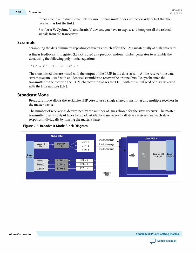
Broadcast ModeBroadcast mode allows the SerialLite II IP core to use a single shared transmitter and multiple receivers inthe master device.
The number of receivers is determined by the number of lanes chosen for the slave receiver. The mastertransmitter uses its output lanes to broadcast identical messages to all slave receivers, and each slaveresponds individually by sharing the master's lanes.
Figure 2-8: Broadcast Mode Block Diagram
Master FPGABroadcast message
Broadcast message
Broadcast message
N-returnlanes
Shared TXLink
RX Link 1
RX Link 2
RX Link N
AtlanticInterface
Shared TXPHY
RX PHY 1
RX PHY 2
RX PHY N
TX Tsv r 1TX Tsv r 2TX Tsv r N
RX Tsv r 1RX Tsv r 2
RX Tsv r N
Slave FPGA N
Light-weightLinklayer
PHYLayer
CDRSERDES
AtlanticInterface
2-18 ScrambleUG-0705
2016.05.02
Altera Corporation SerialLite II IP Core Getting Started
Send Feedback
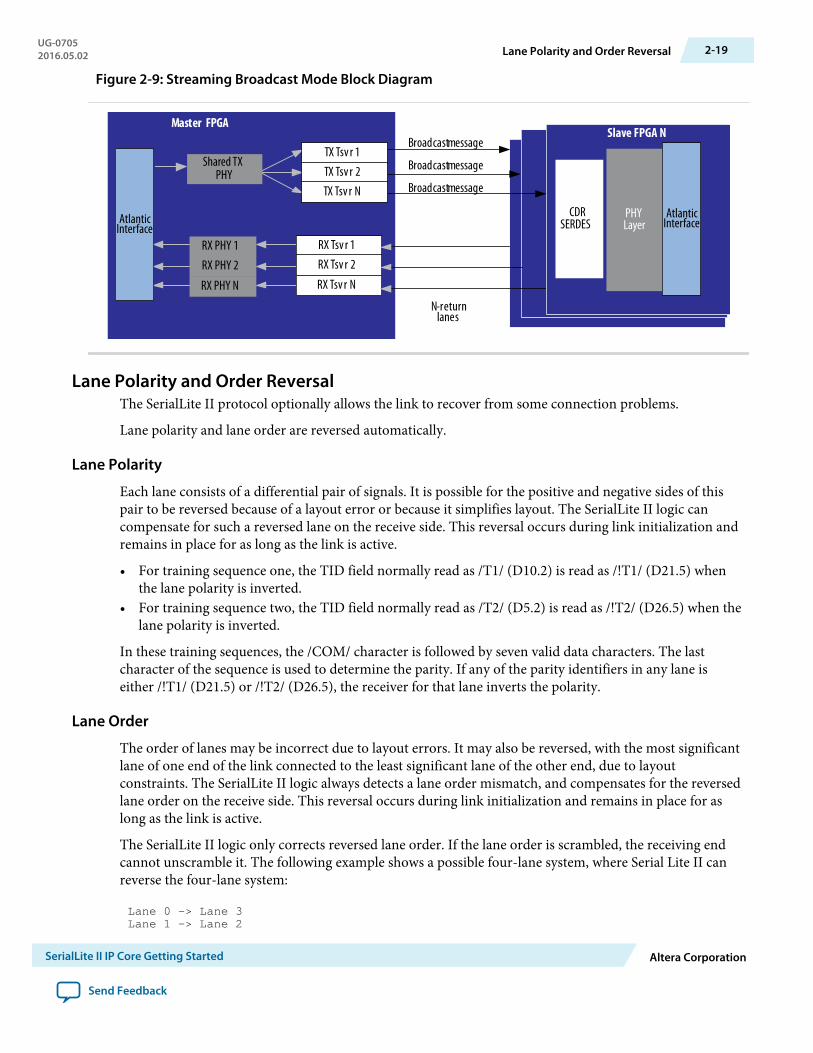
Figure 2-9: Streaming Broadcast Mode Block Diagram
Master FPGABroadcast message
Broadcast message
Broadcast message
N-returnlanes
AtlanticInterface
Shared TXPHY
RX PHY 1
RX PHY 2
RX PHY N
TX Tsv r 1TX Tsv r 2TX Tsv r N
RX Tsv r 1RX Tsv r 2
RX Tsv r N
Slave FPGA N
PHYLayer
CDRSERDES
AtlanticInterface
Lane Polarity and Order ReversalThe SerialLite II protocol optionally allows the link to recover from some connection problems.
Lane polarity and lane order are reversed automatically.
Lane Polarity
Each lane consists of a differential pair of signals. It is possible for the positive and negative sides of thispair to be reversed because of a layout error or because it simplifies layout. The SerialLite II logic cancompensate for such a reversed lane on the receive side. This reversal occurs during link initialization andremains in place for as long as the link is active.
• For training sequence one, the TID field normally read as /T1/ (D10.2) is read as /!T1/ (D21.5) whenthe lane polarity is inverted.
• For training sequence two, the TID field normally read as /T2/ (D5.2) is read as /!T2/ (D26.5) when thelane polarity is inverted.
In these training sequences, the /COM/ character is followed by seven valid data characters. The lastcharacter of the sequence is used to determine the parity. If any of the parity identifiers in any lane iseither /!T1/ (D21.5) or /!T2/ (D26.5), the receiver for that lane inverts the polarity.
Lane Order
The order of lanes may be incorrect due to layout errors. It may also be reversed, with the most significantlane of one end of the link connected to the least significant lane of the other end, due to layoutconstraints. The SerialLite II logic always detects a lane order mismatch, and compensates for the reversedlane order on the receive side. This reversal occurs during link initialization and remains in place for aslong as the link is active.
The SerialLite II logic only corrects reversed lane order. If the lane order is scrambled, the receiving endcannot unscramble it. The following example shows a possible four-lane system, where Serial Lite II canreverse the four-lane system:
Lane 0 -> Lane 3Lane 1 -> Lane 2
UG-07052016.05.02 Lane Polarity and Order Reversal 2-19
SerialLite II IP Core Getting Started Altera Corporation
Send Feedback
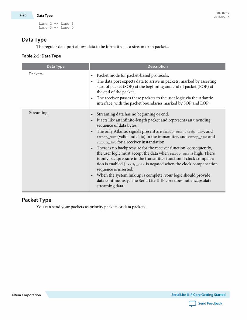
Lane 2 -> Lane 1Lane 3 -> Lane 0
Data TypeThe regular data port allows data to be formatted as a stream or in packets.
Table 2-5: Data Type
Data Type Description
Packets • Packet mode for packet-based protocols.• The data port expects data to arrive in packets, marked by asserting
start of packet (SOP) at the beginning and end of packet (EOP) atthe end of the packet.
• The receiver passes these packets to the user logic via the Atlanticinterface, with the packet boundaries marked by SOP and EOP.
Streaming • Streaming data has no beginning or end.• It acts like an infinite-length packet and represents an unending
sequence of data bytes.• The only Atlantic signals present are txrdp_ena, txrdp_dav, and
txrdp_dat (valid and data) in the transmitter, and rxrdp_ena andrxrdp_dat for a receiver instantiation.
• There is no backpressure for the receiver function; consequently,the user logic must accept the data when rxrdp_ena is high. Thereis only backpressure in the transmitter function if clock compensa‐tion is enabled (txrdp_dav is negated when the clock compensationsequence is inserted.
• When the system link up is complete, your logic should providedata continuously. The SerialLite II IP core does not encapsulatestreaming data. .
Packet TypeYou can send your packets as priority packets or data packets.
2-20 Data TypeUG-0705
2016.05.02
Altera Corporation SerialLite II IP Core Getting Started
Send Feedback

Table 2-6: Differences between Data Packets and Priority Packets
Data Packets Priority Packets (Retry-on-ErrorEnabled)
Priority Packets (Retry-on-Error Disabled)
• A cut-through data flowis implemented for datapackets.
• Packet data istransmitted as soon asenough data is receivedto fill a column, withoutwaiting for the entirepacket to be delivered tothe transmitter.
• This approach providesthe lowest latency.
• There is no packet sizelimitation.
• A cut-through data flow isimplemented for prioritypackets.
• Priority packet data istransmitted as soon asenough data is received tofill a column, withoutwaiting for the entirepacket to be delivered tothe transmitter.
• This approach provides thelowest latency.
• There is no packet sizelimitation.
• Priority packets haveprecedence over datapackets. The SerialLite II IPcore inserts high prioritypackets within a datapacket that is already intransmission (nestingpackets).
• A store-and-forward data flow isimplemented for priority packetsegments.
• Priority packets are broken intosegment-sized bytes that are bufferedand sent across the link.
• The transmission of data does not startuntil a segment or an end of packet hasbeen delivered to the transmitter.
• Priority packets have precedence overdata packets. The SerialLite II IP coreinserts high priority packets within adata packet that is already in transmis‐sion (nesting packets).
• There is also no maximum packet sizelimitation.
Retry-on-ErrorThe retry-on-error mechanism improves the bit error rate of your data.
The retry-on-error parameter provides for segments with errors to be retransmitted, so that only goodsegments are delivered to the Atlantic receive interface. When you turn on the Retry-on-error parameter,all segments sent by the transmitter are acknowledged.
• ACK: The received segment is good and error-free.• NACK: The received segment contains an error.
• If you turn on the Retry-on-error parameter, the transmitter retransmits all segments starting fromthe segment with errors.
• If you turn off the Retry-on-error parameter, the receiver raises a data error.
The segment buffers in the transmitting logic hold segments until they have been acknowledged. Once asegment has been acknowledged by ACK, it is released from the buffer so that the buffer can be used foranother segment. If a segment is acknowledged by NACK, that segment and all segments sent after thatsegment are retransmitted.
The IP core can hold up to seven segments waiting for acknowledgement at once. If more segments arrivewhile all eight buffers are occupied, the priority data port stalls until an acknowledgment is received,freeing up a buffer for the next segment.
UG-07052016.05.02 Retry-on-Error 2-21
SerialLite II IP Core Getting Started Altera Corporation
Send Feedback
The retry-on-error operation proceeds in this sequence:
1. When the receiver receives a good segment, the segment is delivered to the Atlantic interface and anACK acknowledgment is sent back to the transmitter.
2. Any data errors cause the segment to be acknowledged as errored (NACK). Once that happens, thereceiver ignores all incoming data until it receives the retransmitted segment.
3. All segments are numbered internally with a segment ID. The receiver knows which segment it expectsnext, so if the next expected segment has been corrupted or lost, the next received segment has thewrong segment number and the receiver requests a retransmission of the sequence starting with thesegment ID it was expecting.
4. The oldest outstanding segment to be acknowledged has an associated timer, set by the Timeout valueon the Link Layer page in the SerialLite II parameter editor. If an acknowledgment (ACK or NACK) islost or corrupted in transit, the timer expires causing the affected segment and all subsequent segmentsto be retransmitted.
5. The transmitter knows which segment it expects to be acknowledged next. If the next acknowledgmentis not for the expected segment, the transmitter infers that the expected acknowledgment was lost andretransmits the segment in question and all subsequent segments. Only segments that have the correctsegment ID are buffered. The timer starts when the segment is identified as the next segment to beacknowledged.
6. If the timer expires three times in succession, a link error is declared and the link is restarted. You cancontrol the Timeout limit in the SerialLite II parameter editor.
• Do not to set the time out to be too long so the system does not have to wait too long for suchsituations to resolve.
• Do not set the time out to be too short because then the system always times out and the link neverremains up.
Implementation of the retry-on-error mechanism is optional for the priority port. If the Retry-on-errorparameter is turned off, no segment acknowledgments are generated or expected, and all segments aretransmitted without any acknowledgments from the receiver.
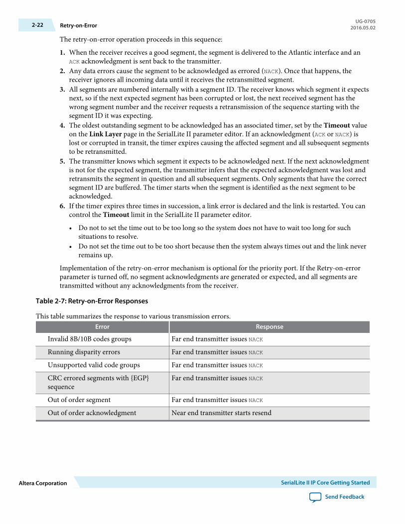
Table 2-7: Retry-on-Error Responses
This table summarizes the response to various transmission errors.Error Response
Invalid 8B/10B codes groups Far end transmitter issues NACK
Running disparity errors Far end transmitter issues NACK
Unsupported valid code groups Far end transmitter issues NACK
CRC errored segments with {EGP}sequence
Far end transmitter issues NACK
Out of order segment Far end transmitter issues NACK
Out of order acknowledgment Near end transmitter starts resend
2-22 Retry-on-ErrorUG-0705
2016.05.02
Altera Corporation SerialLite II IP Core Getting Started
Send Feedback

Figure 2-10: Retry-On-Error Example
This figure shows an example of the retry-on-error operation.
ACK_S; ACK_T; ACK_U
Seg_S; Seg_T; Seg_U
ACK_A; NACK_B
ACK_B; ACK_C
Resend Seg _B; Se g_C
1
5
6
7
3
4
2
Device A Device B
Seg_A; Seg_B; Seg_C
Device A transmits Seg_A, Seg_B, and Seg_C to Device B.At the same time, Device B transmits Seg_S, Seg_T, and Seg_U to Device A.Device B properly receives Seg_A, but detects an error with Seg_B.Device B returns positive acknowledge for Seg_A, but requests retransmission of Seg_B. Device B discards all subsequently received segments until Seg_B is received again.Device A acknowledges the proper reception of Seg_S; Seg_T; and Seg_U.Device A resends all segments starting from Seg_B.Finally, Device B acknowledges the proper reception of Seg_B and Seg_C.
(1)(2)(3)(4)
(5)(6)(7)
Notes:
Flow Control OperationThe flow control feature in the SerialLite II IP core operates by having the receiving end of the link issue aPAUSE instruction to the transmitting end of the link when threshold of the receiver’s FIFO buffer isbreached.
The PAUSE instruction causes the transmitter to cease transmission for specified pause duration. When thepause duration expires, the transmission resumes.
When flow control is used, the FIFO buffer is structured as two sections, threshold and headroom.
UG-07052016.05.02 Flow Control Operation 2-23
SerialLite II IP Core Getting Started Altera Corporation
Send Feedback
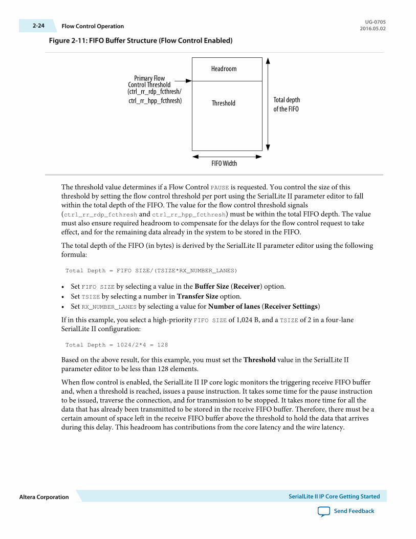
Figure 2-11: FIFO Buffer Structure (Flow Control Enabled)
Threshold
HeadroomPrimary Flow
Control Threshold(ctrl_rr_rdp_fcthresh/ ctrl_rr_hpp_fcthresh) Total depth
of the FIFO
FIFO Width
The threshold value determines if a Flow Control PAUSE is requested. You control the size of thisthreshold by setting the flow control threshold per port using the SerialLite II parameter editor to fallwithin the total depth of the FIFO. The value for the flow control threshold signals(ctrl_rr_rdp_fcthresh and ctrl_rr_hpp_fcthresh) must be within the total FIFO depth. The valuemust also ensure required headroom to compensate for the delays for the flow control request to takeeffect, and for the remaining data already in the system to be stored in the FIFO.
The total depth of the FIFO (in bytes) is derived by the SerialLite II parameter editor using the followingformula:
Total Depth = FIFO SIZE/(TSIZE*RX_NUMBER_LANES)
• Set FIFO SIZE by selecting a value in the Buffer Size (Receiver) option.• Set TSIZE by selecting a number in Transfer Size option.• Set RX_NUMBER_LANES by selecting a value for Number of lanes (Receiver Settings)
If in this example, you select a high-priority FIFO SIZE of 1,024 B, and a TSIZE of 2 in a four-laneSerialLite II configuration:
Total Depth = 1024/2*4 = 128
Based on the above result, for this example, you must set the Threshold value in the SerialLite IIparameter editor to be less than 128 elements.
When flow control is enabled, the SerialLite II IP core logic monitors the triggering receive FIFO bufferand, when a threshold is reached, issues a pause instruction. It takes some time for the pause instructionto be issued, traverse the connection, and for transmission to be stopped. It takes more time for all thedata that has already been transmitted to be stored in the receive FIFO buffer. Therefore, there must be acertain amount of space left in the receive FIFO buffer above the threshold to hold the data that arrivesduring this delay. This headroom has contributions from the core latency and the wire latency.
2-24 Flow Control OperationUG-0705
2016.05.02
Altera Corporation SerialLite II IP Core Getting Started
Send Feedback
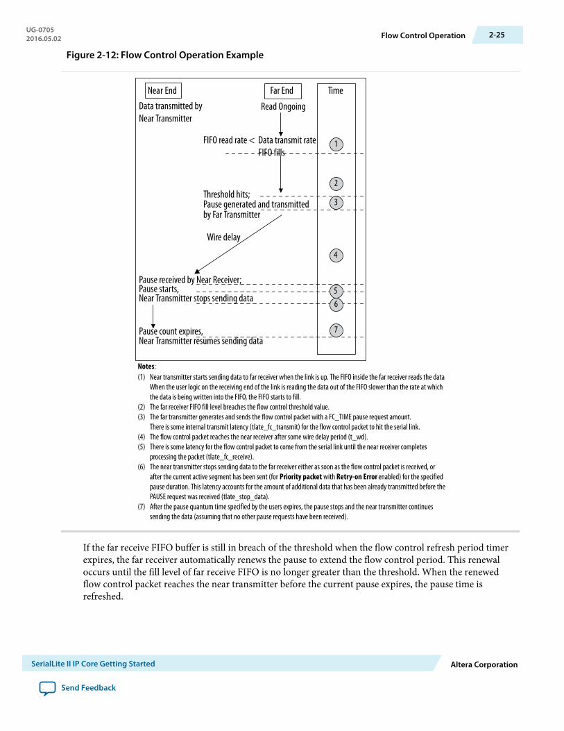
Figure 2-12: Flow Control Operation Example
Near End
Far End
Data transmitted by Near Transmitter
Read Ongoing
Time
1
3
4
2
7
FIFO read rate < Data transmit rateFIFO fills
Threshold hits;Pause generated and transmittedby Far Transmitter
56
Pause received by Near Receiver;Pause starts,Near Transmitter stops sending data
Pause count expires,Near Transmitter resumes sending data
Near transmitter starts sending data to far receiver when the link is up. The FIFO inside the far receiver reads the data.When the user logic on the receiving end of the link is reading the data out of the FIFO slower than the rate at whichthe data is being written into the FIFO, the FIFO starts to fill.The far receiver FIFO fill level breaches the flow control threshold value.The far transmitter generates and sends the flow control packet with a FC_TIME pause request amount. There is some internal transmit latency (tlate_fc_transmit) for the flow control packet to hit the serial link.The flow control packet reaches the near receiver after some wire delay period (t_wd).There is some latency for the flow control packet to come from the serial link until the near receiver completesprocessing the packet (tlate_fc_receive).The near transmitter stops sending data to the far receiver either as soon as the flow control packet is received, orafter the current active segment has been sent (for Priority packet with Retry-on Error enabled) for the specifiedpause duration. This latency accounts for the amount of additional data that has been already transmitted before thePAUSE request was received (tlate_stop_data).After the pause quantum time specified by the users expires, the pause stops and the near transmitter continuessending the data (assuming that no other pause requests have been received).
(1)
(2)(3)
(4)(5)
(6)
(7)
Notes:
Wire delay
If the far receive FIFO buffer is still in breach of the threshold when the flow control refresh period timerexpires, the far receiver automatically renews the pause to extend the flow control period. This renewaloccurs until the fill level of far receive FIFO is no longer greater than the threshold. When the renewedflow control packet reaches the near transmitter before the current pause expires, the pause time isrefreshed.
UG-07052016.05.02 Flow Control Operation 2-25
SerialLite II IP Core Getting Started Altera Corporation
Send Feedback

• This refresh time must be set so that the renewed flow control packets are received by the neartransmitter before the current pause time completes. Set the value of Refresh period to be smaller thanPause quantum time in the Priority Packet Settings or Data Packet Settings in the parameter editor.
• If the refresh period is small, more flow control packets are sent on the link, possibly degrading theperformance of an alternate active port. This is a trade off for the link bandwidth performance.
To overcome head-of-line blocking, every port has its own flow control that suspends the flow of data toeither the priority port or the regular data port, depending on the FIFO buffer status. For example, if thenear transmitter receives a flow control pause request for the priority port, the data on the regular port istransmitted (as long as the regular port is not also being requested to pause).
Selecting the Proper Threshold ValueTo determine FIFO threshold size, you need to factor in the flow control internal latency.
Table 2-8: SerialLite II Flow Control Internal Latency
This table defines the specification value for flow control internal latency. Use this information to determine theminimum FIFO threshold size avoiding starvation during the flow control.
Internal Latency Latency Value (cycles) Description
tlate_fc_
transmit
24 Latency that occurs during RX FIFO breach up to thepoint where the associated flow control link managementpacket is sent out on the link. This includes the time forthe core to generate the link management packet and thetime through the transceiver.
t_wd This value depends onthe data rate and tracelengths in theapplication.
Wire delay between the devices.
tlate_fc_receive 23 + deskew cycles Latency that occurs in the duration when the flow controllink management packet reaches the transceiver pins untilthe IP core processes the request.
• Deskew cycles = 0 for single lane configuration• Deskew cycles = worst case lane to lane skew in the
transceiver
2-26 Selecting the Proper Threshold ValueUG-0705
2016.05.02
Altera Corporation SerialLite II IP Core Getting Started
Send Feedback
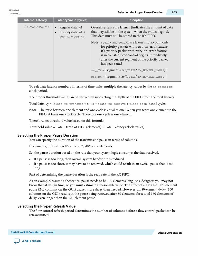
Internal Latency Latency Value (cycles) Description
tlate_stop_data • Regular data: 41• Priority data: 41 +
seg_TX + seg_RX
Overall system core latency (indicates the amount of datathat may still be in the system when the PAUSE begins).This data must still be stored in the RX FIFO.
Note: seg_TX and seg_RX are taken into account onlyfor priority packets with retry-on-error feature.If a priority packet with retry-on-error featureis in transfer, flow control begins immediatelyafter the current segment of the priority packethas been sent.]
seg_TX = [segment size/(TSIZE* TX_NUMBER_LANES)]
seg_RX = [segment size/(TSIZE* RX_NUMBER_LANES)]
To calculate latency numbers in terms of time units, multiply the latency values by the tx_coreclockclock period.
The proper threshold value can be derived by subtracting the depth of the FIFO from the total latency.
Total Latency = [tlate_fc_transmit + t_wd + tlate_fc_receive + tlate_stop_data] cycles
Note: The ratio between one element and one cycle is equal to one. When you write one element to theFIFO, it takes one clock cycle. Therefore one cycle is one element.
Therefore, set threshold value based on this formula:
Threshold value = Total Depth of FIFO (elements) – Total Latency (clock cycles)
Selecting the Proper Pause DurationYou can specify the duration of the transmission pause in terms of columns.
In elements, this value is 8/TSIZE to 2,040/TSIZE elements.
Set the pause duration based on the rate that your system logic consumes the data received.
• If a pause is too long, then overall system bandwidth is reduced.• If a pause is too short, it may have to be renewed, which could result in an overall pause that is too
long.
Part of determining the pause duration is the read rate of the RX FIFO.
As an example, assume a theoretical pause needs to be 100 elements long. As a designer, you may notknow that at design time, so you must estimate a reasonable value. The effect of a TSIZE-2, 120-elementpause (240 columns on the GUI) causes more delay than needed. However, an 80-element delay (160columns on the GUI) results in the pause being renewed after 80 elements, for a total 160 elements ofdelay, even longer than the 120-element pause.
Selecting the Proper Refresh ValueThe flow control refresh period determines the number of columns before a flow control packet can beretransmitted.
UG-07052016.05.02 Selecting the Proper Pause Duration 2-27
SerialLite II IP Core Getting Started Altera Corporation
Send Feedback

The stat_tc_rdp_thresh_breach, stat_tc_hpp_thresh_breach, stat_fc_hpp_retransmit, andstat_tc_fc_hpp_retransmit status signals indicate whether the refresh period is set appropriately. Ifstat_tc_rdp_thresh_breach or stat_tc_hpp_thresh_breach (which indicates that the RX FIFO is stillbreached) is still asserted after the FC refresh period (based on the value set), the far transmitter generatesanother flow control packet (based on the value set at the Pause Quantum Time option) and sends it out,causing the stat_fc_hpp_retransmit or stat_tc_fc_hpp_retransmit to be asserted.
External Flow Control (When RX FIFO Size is 0)The SerialLite II IP core supports an external flow control when the RX FIFO size is zero.
The rxrdp_dav and rxhpp_dav input signals are provided to activate flow control to pause the datatransmission when the corresponding regular port or priority data port is selected. Drive rxrdp_dav lowwhen the fill level of your external FIFO has been breached. This action triggers the flow control pauserequest. When this signal is high, no flow control requests is generated.
Transmit/Receive FIFO BuffersThe SerialLite II IP core automatically sets the width of the receive FIFO buffers at TSIZE bytes per lane.
• The transmit FIFO buffers are used by the transmitting end of the SerialLite II link to store data to betransmitted across the high-speed serial link.
• The receive FIFO buffers are used by the receiving end of the SerialLite II link to store data forpresentation to the Atlantic interface and eventual consumption by the system logic.
The size of the FIFO buffers are affected by these factors:
• Flow control—If flow control is enabled, the FIFO buffer size should change to account for thethresholds that must be set.
• Pause duration—When optimizing against starvation during flow control, the pause duration affectsthe FIFO buffer size.
• Number of packets (and packet sizes)—If you want to use a store-and-forward FIFO (using theeop_dav and a high threshold), the FIFO must be big enough to hold a full packet at minimum.
• Wire delay and bit rate—The wire propagation delay and the bit rate change the wire latency, whichmust be accommodated if flow control is used.
Figure 2-13: Atlantic FIFO Buffer Structure
Width set automaticall y
Threshold
Headroom
FTL/FTH
Totaldepth
2-28 External Flow Control (When RX FIFO Size is 0)UG-0705
2016.05.02
Altera Corporation SerialLite II IP Core Getting Started
Send Feedback
The FIFO buffer threshold low (FTL), ctl_rxrdp_ftl/ctl_rxhpp_ftl, value for receiver variationscontrols when the rxrdp_dav/rxhpp_dav signals are asserted for the read side of the FIFO buffer,respectively. If the fill level of the buffer is higher than the FTL value, the rxrdp_dav/rxhpp_dav signal isasserted indicating that there is a burst of data available.
Note: There is no requirement to wait for the rxrdp_dav/rxhpp_dav signal to be asserted; you can readfrom the buffer at any time by asserting the rxrdp_ena/rxhpp_ena signal at all times andqualifying the data with the rxrdp_val/rxhpp_val signal. The FIFO buffer has built-in underflowprotection, such that an underflow condition does not exit.
The receiver Atlantic FIFO buffers include an end-of-packet based data available feature which can beturned on by asserting the ctl_rxrdp_eopdav/ctl_rxhpp_eopdav signals. The end-of-packet featuredetermines whether the dav remains high: if the signal is asserted, and there is an end-of- packet beneaththe FTL threshed, the dav signal remains high until the end-of-packet is read out of the FIFO buffer.Otherwise, if the signal is not asserted, the dav signal only remains high when the fill level of the buffer ishigher than the FTL value.
ctl_rxhpp_fth and ctl_rxrdp_fth are the threshold levels for the high priority and regular data portson the receiver Atlantic FIFO buffers. When the data fill level is higher than the threshold level set byctl_rxhpp_fth or ctl_rxrdp_fth, or dav = 1, it means that there a large amount of data ready to befetched at the FIFO buffer. You must set these threshold levels based on your design requirements, andensure that the FIFO buffer does not underflow. You may also set the threshold levels to segment size of apriority packet; or to the lowest level so that you can fetch data as soon as it is stored in the FIFO buffer.
You can set ctl_rxhpp_ftl to 1 element unit so that it fetches the data from the RX FIFO buffer as soonas there is data available. If you want to store some data before fetching it, you can raise the thresholdlevel. The FIFO buffer threshold high (ctl_txrdp_fth/ctl_txhpp_fth) value for transmitter variationscontrols when the txrdp_dav/txhpp_dav signals are asserted and deasserted for the write side of the FIFObuffer, respectively. The txrdp_dav signal indicates when there is room available to write new data intothe FIFO buffer, and is asserted when the fill level of the FIFO is less than the FTH setting, and deassertedwhen the fill level of the FIFO is greater than the FTH.
For example, if FTH is five, and the fill level is four, the txrdp_dav/txhpp_dav signal is high, indicatingthat the user can write data into the FIFO. If the fill level for this example is six, the txrdp_dav/txhpp_davsignal is low, indicating that the user should stop writing data into the FIFO. ctl_txhpp_fth andctl_txrdp_fth are the threshold levels for the high priority and regular data ports on the transmitterAtlantic FIFO buffers. When the data fill level at the FIFO buffer is lower than the threshold level set byctl_txhpp_fth or ctl_txrdp_fth, or dav = 1, it means that there are plenty of spaces available for datato write into the buffer. You must set these threshold levels high so that the user logic knows whenever theFIFO buffer has available spaces for data buffering and to ensure that overflow does not occur. However,these threshold settings should not exceed the FIFO depth.
For example, if the transmitter buffer size is 4,096 bytes, and the transmitter FIFO depth is 2,048 elementunits, you should set the level of ctl_txhpp_fth = 250 element units.
TSIZE = 2, and one FIFO element = 2 bytes
Maximum TX FIFO level (TX 8 lane) = 2,048/8 = 256 element units
Note: You can set any value below 256 element units for ctl_txhpp_fth; Altera recommends a level of250 element units or 8'hFA.
The threshold levels on both the transmitter and receiver Atlantic FIFO buffers differ according toimplementation. They may depend on the data traffic, the FIFO depth, and the clock frequencies for read
UG-07052016.05.02 Transmit/Receive FIFO Buffers 2-29
SerialLite II IP Core Getting Started Altera Corporation
Send Feedback
and write. Based on your design, you can gauge the usual fill level of the FIFO buffers and determine theappropriate threshold levels.
Data Integrity Protection: CRCIf you need error protection, you may add CRC checking to your packet.
The CRC is automatically generated in transmission and is automatically checked on reception. On thedata port, a CRC check failure results in the packet being marked as bad using the rxrdp_err/rxhpp_errsignal on the Atlantic interface. You decide independently for each port whether CRC usage is enabled.
The SerialLite II IP core supports both 16-bit and 32-bit CRC algorithms. You decide which CRCalgorithm to use independently for each port.
• The 16-bit algorithm generates a two-byte result, and uses the following polynomial equation:
G(x) = X16 + X12 + X5 + 1
• The 32-bit algorithm generates a four-byte result, and uses the following polynomial equation:
G(x) = X32 + X26 + X23 + X22 + X16 + X12 + X11 + X10 + X8 + X7 + X5 + X4 + X2 + X + 1
The 16-bit version provides excellent protection for packets smaller than about 1 KBytes. For largerpackets, CRC-32 can be considered, but it requires significantly more logic, especially in implementationsrequiring many lanes. At 16 lanes, CRC-32 logic may constitute as much as half of the logic of the entireSerialLite II instantiation. Therefore, CRC-32 should only be used when absolutely necessary.
Transceiver ConfigurationThe transceiver IP core offers several configuration options that can be set based on board-levelconditions, design constraints, or other application-specific requirements, to ensure the proper operationof the serial link.
Note: The Configure Transceiver option is available only for Arria II GX and Stratix IV devices. If youselect Arria V, Cyclone V, or Stratix V as the target device family, you are required to instantiatethe Custom PHY IP core as the hard transceiver. For Arria 10 devices, contact your local Alterarepresentative or file a Service Request (SR).
Related InformationIP Core Configuration for Arria 10, Arria V, Cyclone V, and Stratix V Devices on page 3-19
Voltage Output Differential (VOD) Control SettingsThe Stratix IV transceivers allow you to set the VOD to handle different length, backplane, and receiverrequirements.
A range from 200 to 1,200 mV is supported for Stratix IV devices. Arria II GX devices have a fixed value,which cannot be changed. The range is decoded using the GUI integer value and the on-chip transmitterprogrammable termination values.
2-30 Data Integrity Protection: CRCUG-0705
2016.05.02
Altera Corporation SerialLite II IP Core Getting Started
Send Feedback

Table 2-9: VOD Control Settings
This table shows how the VOD value you chose in the SerialLite II parameter editor corresponds to the mV value.The VOD value is 0 by default.
VOD Value (Per Lane) 100 Ω (mV) Stratix IV
0 200
1 400
2 600
3 700
4 800
5 900
6 1,000
7 1,200
Pre-Emphasis Control SettingsThe programmable pre-emphasis setting boosts the high frequencies in the transmit data signal, whichmay be attenuated by the transmission medium.
The pre-emphasis setting maximizes the data eye opening at the far-end receiver, which is particularlyuseful in lossy transmission mediums.
Transmitter Buffer Power (VCCH)You can set your preferred VCCH value to the transmit and receive pins.
1. In the Quartus Prime software, on the Assignments menu, click Assignment Editor.2. In the <<new>> row, in the To column, double-click and type rxin to set value for the receive pin.3. Double-click in the Assignments Name column, and click I/O Standard (Accepts wildcards/groups).
The entry is set to I/O Standard.4. Double-click in the Value column and click 1.4-V PCML or 1.5-V PCML.5. In the new <<new>> row, repeat steps 2 to 4 to set the value for the transmit pin (txout).
Transceiver Reconfiguration BlockWhen you use an Arria II GX, Arria V, Arria 10, Cyclone V, Stratix IV, or a Stratix V device, you caninstantiate a transceiver reconfiguration block.
The transceiver reconfiguration block dynamically changes the following physical media attachment(PMA) settings:
• Pre-emphasis• Equalization• VOD• Offset cancellation
Note: For analog settings, there are no restrictions on using dynamic reconfiguration.
UG-07052016.05.02 Pre-Emphasis Control Settings 2-31
SerialLite II IP Core Getting Started Altera Corporation
Send Feedback

When you use a transceiver-based device, the ALTGX interface allows you to modify the parameterinterface with a reconfiguration block. The altgx_reconfig block is not instantiated, but the Quartus-generated wrapper provides the ports that interface to the altgx_reconfig block.
If you choose to use an altgx_reconfig block, you must instantiate the altgx_reconfig block andconnect the associated signals to the corresponding SerialLite II IP core top-level signals (tie thereconfig_fromgxb, reconfig_clk, and reconfig_togxb ports to the altgx_reconfig block).
Note: For Arria 10, Arria II GX, and Stratix IV devices, you must instantiate the transceiver reconfigura‐tion block on the devices, because these device transceivers require offset cancellation. Your ArriaII GX or Stratix IV design can compile without the dynamic reconfiguration block but it cannotfunction correctly in hardware. For Arria V, Cyclone V, and Stratix V devices, you need to includea dynamic reconfiguration block for the offset cancellation to occur.
ALTGX Support SignalsThe ALTGX support signals are only present on variants that use the Arria II GX and Stratix IVintegrated PHY.
The ALTGX support signals are connected directly to the ALTGX instance. In many cases these signalsmust be shared with ALTGX instances that are implemented in the same device.
Table 2-10: ALTGX Support Signals
Signal Direction Description
cal_blk_clk Input The cal_blk_clk input signal is connected to the ALTGXcalibration block clock (cal_blk_clk) input. All instancesof ALTGX in the same device must have their cal_blk_clkinputs connected to the same signal because there is onlyone calibration block per device. This input should beconnected to a clock operating as recommended by theArria II GX Device Handbook or the Stratix IV DeviceHandbook.
reconfig_clk Input The reconfig_clk input signal is the ALTGX dynamicreconfiguration clock. This signal must be connected asdescribed in the Arria II GX Device Handbook or the StratixIV Device Handbook if the ALTGX dynamic reconfigurationblock is used. Otherwise, this signal must be set to 1'b0.
reconfig_togxb Input The reconfig_togxb [N:0] input signal is driven from anexternal dynamic reconfiguration block. The signal supportsthe selection of multiple transceiver channels for dynamicreconfiguration. This signal must be connected as describedin the Arria II GX Device Handbook or the Stratix IV DeviceHandbook if the external dynamic reconfiguration block isused. Otherwise, you must set this signal to 4'b0010 forArria II GX and Stratix IV devices.
N value is 3 for Arria II GX and Stratix IV devices.
2-32 ALTGX Support SignalsUG-0705
2016.05.02
Altera Corporation SerialLite II IP Core Getting Started
Send Feedback

Signal Direction Description
reconfig_fromgxb Output The reconfig_fromgxb output signal is driven to anexternal dynamic reconfiguration block. The width of thisbus depends on the number of lanes (it may requiremultiple transceiver QUAD blocks), and the device family(for Arria II GX and Stratix IV, the bus is wider due to offsetcancellation support).
This signal identifies the transceiver channel whose settingsare being transmitted to the dynamic reconfiguration. Thissignal must be connected as described in the Arria II GXDevice Handbook or the Stratix IV Device Handbook if theexternal dynamic reconfiguration block is used. Otherwise,leave this signal unconnected.
For Arria II GX and Stratix IV devices, you must use thedynamic reconfiguration block because they require offsetcancellation.
gxb_powerdown Input gxb_powerdown resets and powers down all circuits in thetransceiver block. This signal does not affect the refclkbuffers and reference clock lines.
All the gxb_powerdown input signals of cores placed in thesame quad should be tied together. The gxb_powerdownsignal should be tied low or should remain asserted for atleast 2 ms whenever it is asserted.
Related InformationSerialLite II Implementation in Stratix V DevicesYou can use the SerialLite II implementation in Stratix V devices as a guideline to connect the transceiversignals to the core for Arria V, Cyclone V, and Stratix V devices.
Error HandlingThe SerialLite II IP core does error checking and has an interface to view local errors. The errors arecategorized, and the effect of an error depends on the type of error that occurs.
The SerialLite II IP core has three error types:
• Data error• Link error• Catastrophic error
UG-07052016.05.02 Error Handling 2-33
SerialLite II IP Core Getting Started Altera Corporation
Send Feedback

Table 2-11: Error Summary
This table summarizes the causes and results of the SerialLite II error types.Error Type Cause Action
Data • Invalid 8B/10B codes groups• Running disparity errors• Unsupported valid code groups• Link protocol violation• LMP with BIP error• CRC error• Unexpected channel number• Out of order packet• Out of order acknowledgment (if
Retry-on-error is enabled)
Two possibilities:
• If Retry-on-error is enabled and the packet is apriority packet, request retransmission.
• Otherwise, mark the packet as bad and forwardit to the user link layer.
Link • Eight consecutive {|TS1|}sequences received in all lanessimultaneously
• Loss of character alignment• Loss of lane alignment• Loss of characters from
underflow/overflow• Data error threshold exceeded• Retry-on-error timer expired
three times
Trigger link initialization
Catastrophic • LSM cannot reverse polarity• LSM cannot reorder lanes
SerialLite II enters nonrecoverable state
PacketsMarked Bad
{EBP} marked packet Received packet is marked as bad through therxrdp_err or rxhpp_err signals, and forwarded tothe user link layer.
Error signals, such as txrdp_err and txhpp_err, are asserted by user logic.
• When txrdp_err is asserted with txrdp_eop, the packet is marked with the end of bad packet {EBP}marker.
• The txrdp_err signal is ignored when it is not asserted with txrdp_eop.• When the txhpp_err is asserted and the Retry-on-error feature is turned off, the packet is marked
with the {EBP} marker.• When the txhpp_err is asserted and the Retry-on-error feature is turned on, the packet is not
transmitted and is silently dropped.
Optimizing the ImplementationThere are a number of steps you can take to optimize your design, depending on your goals.
2-34 Optimizing the ImplementationUG-0705
2016.05.02
Altera Corporation SerialLite II IP Core Getting Started
Send Feedback
The features selected in your SerialLite II configuration have a substantial impact on both resource utiliza‐tion and performance. Because of the number of different combinations of options that are available, it isdifficult to generalize the performance or resource requirements of a design. In addition, the performanceof a SerialLite II link in isolation is different from the performance of the same link instantiated alongsidelarge amounts of other logic in the device.
For the most part, the steps you take to improve performance or resource utilization are similar to thesteps you would take for any other design.
Improving PerformancePerformance is the factor that depends most on what other logic exists in the device.
If the SerialLite II IP core is competing with other logic for routing resources, inefficient routing couldcompromise speed.
Table 2-12: Factors Comprising Speed
Factors Description
Feature selection These features impact speed more significantly:
• Lane count—running more lanes more slowly reduces the operatingfrequency required (but uses more logic resources).
• CRC—the CRC generation and checking logic degrades perform‐ance and latency. In particular, if you are using CRC-32, evaluatecarefully whether the extra protection over CRC-16 is reallyworthwhile, because CRC-16 has less impact on speed.
• Receive FIFO buffer size—large FIFO buffers increase fanout andmay require longer routing to extend further inside the device.
Your system may require some of these features, but if any are optionalor can be reconsidered, this may help your performance. Beforemaking any changes, verify that the feature you want to change is inthe critical speed path.
Running different seeds If your first attempt at hitting performance is close to the requiredfrequency, try running different placement seeds. This technique oftenyields a better result.
For information on seed specification and improving speed refer to theCommand-Line Scripting and the Design Space Explorer chapters in theQuartus Prime Handbook.
Limiting fanout Depending on the number of lanes and the size of memories youchoose, fanout can impact performance.
Limiting the fanout during synthesis causes replication of high-fanoutsignals, improving speed. If high-fanout signals are the critical path,limiting the fanout allowed can help.
Refer to the Quartus Prime Handbook for more information onlimiting fanout.
UG-07052016.05.02 Improving Performance 2-35
SerialLite II IP Core Getting Started Altera Corporation
Send Feedback

Factors Description
Floorplanning The SerialLite II IP core does not come with any placement constraints.The critical paths depend on where the Fitter places SerialLite II logicin the device, as well as the other logic in the device. You can usestandard floorplanning techniques to improve performance.
Refer to the Quartus Prime Handbook for more information onfloorplanning.
Related InformationQuartus Prime Standard Edition Handbook Volume 2: Design Implementation and OptimizationProvides more information about design optimization.
Minimizing Logic UtilizationThe amount of logic required for a SerialLite II link depends heavily on the features you choose.
Table 2-13: Features Affecting Logic Usage
Features Description
Lane count Running fewer lanes at higher bit rates, if possible, uses less logic (butplaces more of a burden on meeting performance).
CRC Significant savings can be made by eliminating CRC, or in particular,moving from CRC-32 to CRC-16 in high-lane-count designs. If you areusing CRC- 32, evaluate carefully whether the extra protection overCRC-16 is really worthwhile, because CRC-16 uses far fewer resources.
Flow control This feature requires logic to monitor the FIFO buffer levels and togenerate and act upon PAUSE instructions.
Streaming mode Use this mode if packet encapsulation is not required. The link-layerportion of the SerialLite II IP core contains a significant amount oflogic, which is reduced to zero in streaming mode.
Minimizing Memory UtilizationThe amount of memory required for a SerialLite II link depends heavily on the features you choose.
To obtain a measure of the memory required for your configuration, you must synthesize the design.
Table 2-14: Features Affecting Memory Usage
Features Description
Lane count The lane count establishes the bus widths internally, and mostmemories used scale almost directly with the number of lanes selected.Running fewer lanes at higher bit rates, if possible, uses less memory(but places more of a burden on meeting performance).
Receive FIFO buffer size You can minimize memory usage by not adding significant amounts ofmargin to the minimum specified sizes.
2-36 Minimizing Logic UtilizationUG-0705
2016.05.02
Altera Corporation SerialLite II IP Core Getting Started
Send Feedback

SerialLite II IP Core Functional Description 32016.05.02
UG-0705 Subscribe Send Feedback
The SerialLite II IP core consists of parameterized logic and a parameterized testbench.
The SerialLite II IP core is divided into two main blocks: a protocol processing portion (data link layer)and a high-speed front end (physical layer).
• The protocol processing portion features Atlantic FIFO buffers for data storage or clock domaincrossing, and data encapsulation and extraction logic.
• The high-speed front end contains a link state machine (LSM) and serializer/deserializer (SERDES)blocks.
• The SERDES blocks contain optional high-speed serial clock and data recovery (CDR) logicimplemented with high-speed serial transceivers.
SerialLite II MegaCore Function
PHY Layer (PCS)
n-bit
DataFlow
n-bit
n-bit
Receiver
n-bit
AtlanticInterface
AtlanticInterface
DataFlow
SERDES
SERDES
SERDES
SERDES
Word AlignerTraining Detection
Link State Machine & Generator
Transmitter
SerialLite IIInterface
SerialLite IIInterface
Link Layer
© 2016 Altera Corporation. All rights reserved. ALTERA, ARRIA, CYCLONE, ENPIRION, MAX, MEGACORE, NIOS, QUARTUS and STRATIX words and logos aretrademarks of Altera Corporation and registered in the U.S. Patent and Trademark Office and in other countries. All other words and logos identified astrademarks or service marks are the property of their respective holders as described at www.altera.com/common/legal.html. Altera warrants performanceof its semiconductor products to current specifications in accordance with Altera's standard warranty, but reserves the right to make changes to anyproducts and services at any time without notice. Altera assumes no responsibility or liability arising out of the application or use of any information,product, or service described herein except as expressly agreed to in writing by Altera. Altera customers are advised to obtain the latest version of devicespecifications before relying on any published information and before placing orders for products or services.
ISO9001:2008Registered
www.altera.com101 Innovation Drive, San Jose, CA 95134
Related InformationSerialLite II IP Core Testbench on page 4-1
Atlantic InterfaceThe Atlantic interface provides a standard mechanism for delivering data to, and accepting data from, theSerialLite II IP core.
It is a full-duplex, synchronous point-to-point connection interface that supports a variety of data widths.The width of the Atlantic interface is determined by the number of lanes and the transfer size.
The SerialLite II IP core allows you to create one or two data ports: one for regular data and one forpriority data.
• Each port has a full Atlantic interface.• In the transmit direction of each type of port, an Atlantic dual clock domain FIFO buffer is
implemented.• The receiver dual clock domain Atlantic FIFO buffer is optional.
The SerialLite II IP core is an Atlantic interface slave when the Atlantic FIFO buffer is implemented(when the function is not in streaming mode, and the buffer size is not zero). Otherwise, the IP core is anAtlantic interface master. The logic that drives data into the SerialLite II IP core or receives data from theSerialLite II IP core is referred as the system logic.
3-2 Atlantic InterfaceUG-0705
2016.05.02
Altera Corporation SerialLite II IP Core Functional Description
Send Feedback

Figure 3-1: Transmitting and Receiving SerialLite II Data Packets
This timing diagram shows how the data packets are transmitted and received through the Atlanticinterface.
Transmitter
01 02
b1
b1
03
01 02 03
Receiver
clk
txrdp_sop
txrdp_eop
txrdp_dat
txrdp_adr
txrdp_dav
txrdp_ena
rxrdp_sop
rxrdp_eop
rxrdp_adr
rxrdp_dat
rxrdp_dav
On the transmitter side:
• The IP core sends the user input data packets to the Atlantic interface when the txrdp_ena signal isasserted (txrdp_ena pin is level triggered).
• The data packets go through several internal processes in the SerialLite II data link layer and physicallayer, including all packet framing, CRC, and 8B/10B generation, and bit serializing.
• These internal processes produce some core latency of approximately 21 clock cycles to finally send thepackets to the High Speed Serial Interface (HSSI) link.
• The latency calculation is based on the tx_coreclock frequency and is counted from the first datapresented at the Atlantic interface on the transmitter side to the first data that appeared at the HSSI.
On the receiver side:
• The IP core transmits the data packets through the HSSI link and the data packets go through anotherSerialLite II IP core.
• In the other SerialLite II IP core, the same reverse processes are done in the SerialLite II data link layerand physical layer to strip off the framing and return the raw data back in the Atlantic interface.
• The data are presented at the Atlantic interface after approximately 25 clock cycles of latency.• The latency is counted from the first data that appeared at the HSSI to the first data that reaches the
Atlantic interface on the receiver side.
UG-07052016.05.02 Atlantic Interface 3-3
SerialLite II IP Core Functional Description Altera Corporation
Send Feedback
Note: However, these latencies are based on the simulations and parameters set in the testbench. Thelatencies vary depending on different designs and implementations, and the fill levels of theAtlantic FIFO buffer in designs where the fill levels are used.
High-Speed Serial InterfaceThe high-speed serial interface always appears at the external device pins.
The high-speed interface consists of the differential signals that carry the high-speed data between the twoends of a link.
SerialLite IIMegaCore
(Near)
SerialLite II
(Remote)
txout
rxin
rxin
txoutFunction
MegaCoreFunction
High-Speed Serial Interface
Clocks and Data RatesA SerialLite II link has two distinct clock rates: the core clock rate and the bit rate.
The core clock rate is the rate of the clock the internal logic is running at. This clock controls the FPGAlogic and is a derived clock from the phase-locked loops (PLLs). The transmitter and receiver both havetheir own core clocks, tx_coreclock and rrefclk respectively.
To determine the clock frequency for tx_coreclock and rrefclk, use the following formula:
Core clock frequency = Data Rate (Mbps)/(TSIZE×10)
For example, if the data rate is 3,125 Mbps, and the TSIZE is 2, then:
Core clock frequency = 3,125/(2×10) = 156.25 MHz
Aggregate BandwidthThe bit rate specifies the rate of data transmission on a single lane.
3-4 High-Speed Serial InterfaceUG-0705
2016.05.02
Altera Corporation SerialLite II IP Core Functional Description
Send Feedback

In a multi-lane configuration, the total available bandwidth is the single-lane bit rate multiplied by thenumber of lanes. For example, calculate the bandwidth for a variation using 8B/10B encoding and aninternal data path of 8 bits (transfer size is equal to 1), and the number of lanes is equal to 4.
In this mode, the input data bus into the processor portion is 36 bits wide (32 bits of raw data and 4 bits ofcontrol information). With the additional bits per byte (due to 8B/10B encoding) for control information,the data bus size being transmitted from the byte alignment logic into the protocol-processing portion ofthe IP core is equal to the number of lanes × 10 (due to 8B/10B encoding). Thus for 4 lanes, the data bussize is equal to 40 bits (4×10 =40).
For example, a 32-byte packet. Count the number of 32-bit wide rows that are transmitted into theprotocol-processing portion. The result is 8 rows (32 bytes/4 bytes) of solid data, plus one additional rowfor the start-of-packet marker row and the end-of-packet marker row (no CRC) which equals 9 rows of 40bits.
• For a 32-byte packet, given a link rate of 800 Mbps × 4 = 3.2 Gbps, the transfer equals:
• data bits: 256• bits sent: 360• 256/360 × 3.2 = 2.276 Gbps
• For a 64-byte packet, given a link rate of 800 Mbps × 4 = 3.2 Gbps, the transfer equals:
• data bits: 512• bits sent: 680• 512/680 × 3.2 = 2.409 Gbps
• For a 128-byte packet, given a link rate of 800 Mbps × 4 = 3.2 Gbps, the transfer equals:
• data bits: 1, 024• bits sent: 1, 320• 1,024/1, 320 × 3.2 = 2.482 Gbps
External Clock ModesYou can configure the SerialLite II IP core to use one of two clock modes: synchronous or asynchronous.
• A synchronous configuration is used for a link where both ends are on the same board or on twoboards driven by the same system clock.
• An asynchronous configuration is used when the two ends of the link are on different boards, eachhaving its own independent clock source.
UG-07052016.05.02 External Clock Modes 3-5
SerialLite II IP Core Functional Description Altera Corporation
Send Feedback

Figure 3-2: Synchronous Mode
FPGA 1 FPGA 2
RefClk
CDRLanes
Figure 3-3: Asynchronous Mode
FPGA 1 FPGA 2
RefClk1
CDRLanes
RefClk2
Internal Clocking ConfigurationsFor Arria V, Arria 10, Cyclone V, and Stratix V configurations, you must identify the PLL reference clockfrequency of the Custom PHY IP core and set the value accordingly in the.sdc file of the SerialLite II IPcore for design integration between both cores.
When you generate a custom IP core, the IP core generates a Tcl script ((<variation name>_constraints.tcl). These settings are automatically written to your project directory when you run thegenerated Tcl script.
SerialLite II Deskew SupportYou can use the SerialLite II deskew information to ensure trace length differences do not exceed thetiming budget.
Table 3-1: SerialLite II Deskew Tolerance
The values include worst case lane–to–lane skew in the transceivers. To calculate in terms of time units, multiplythe value in this table by the tx_coreclock clock period.
Transfer Size Max Deskew (Cycles)
1 14
2 6
3-6 Internal Clocking ConfigurationsUG-0705
2016.05.02
Altera Corporation SerialLite II IP Core Functional Description
Send Feedback
Transfer Size Max Deskew (Cycles)
4 2
SerialLite II Clocking StructureThe SerialLite II IP core clock structures vary based on the configuration parameters.
The following diagrams show the SerialLite II IP core clock structures, which vary based on the configura‐tion parameters.
Figure 3-4: Full-Featured Clock Structure
slite2_top
XCVR
Word Aligner (&Training Pattern
Detection),[Link StateMachine]
TX Coren-bit
n-bit
RX Core
n-bit
Atlantic
#n SLITE2High
SpeedLinks
#m SLITE2High
SpeedLinks
Atlantic
Atlantic
Atlantic
Regular
Priority
Priority
Regular
PComp_FIFO_0
ByteSerializer
ByteSerializer
PComp_FIFO_n-1
ByteDeserializer
ByteDeserializer
n-bit
rxrdp_clk
rxhpp_clk
txhpp_clk
txrdp_clk
rrefclk
rcvd_clk0
rcvd_clkn-1
trefclk
tx_coreclkRREFCLK
mreset_n
Reset Sync
tx_coreclk
rcvd_clk_out[n-1:0] (1)
Freq OffRemoval
Freq OffRemoval
ATLFIFO
ATLFIFO
ATLFIFO
ATLFIFO
rrefclk
rrefclk
TrainingGenerator [LinkState Machine]
TXPLL
tx_coreclk
tx_coreclk
tx_coreclk
tx_coreclk
Note:(1) Individual recovered clocks (one per channel).
UG-07052016.05.02 SerialLite II Clocking Structure 3-7
SerialLite II IP Core Functional Description Altera Corporation
Send Feedback
Figure 3-5: No Receiver FIFO Buffers Clock Structure
slite2_top
XCVR
TX Coren-bit
n-bit
RX Core
n-bit
#n SLITE2High
SpeedLinks
#m SLITE2High
SpeedLinks
Atlantic
Atlantic
AtlanticRegular(tx_coreclock
domain)
Priority
Regular
PComp_FIFO_0
ByteSerializer
ByteSerializer
PComp_FIFO_n-1
ByteDeserializer
ByteDeserializer
n-bit
txhpp_clk
txrdp_clk
rcvd_clk0
rcvd_clkn-1
tx_coreclockRREFCLK
mreset_n
Reset Sync
tx_coreclock
rcvd_clk_out[n-1:0] (1)
Freq OffRemoval
Freq OffRemoval
ATLFIFO
ATLFIFO
rrefclk
rrefclk
AtlanticPriority(tx_coreclock
domain)
Word Aligner (&Training Pattern
Detection),[Link StateMachine]
TrainingGenerator [LinkState Machine]
trefclk
TXPLL
tx_coreclock
tx_coreclock
tx_coreclock
tx_coreclock
Note:(1) Individual recovered clocks (one per channel).
3-8 SerialLite II Clocking StructureUG-0705
2016.05.02
Altera Corporation SerialLite II IP Core Functional Description
Send Feedback
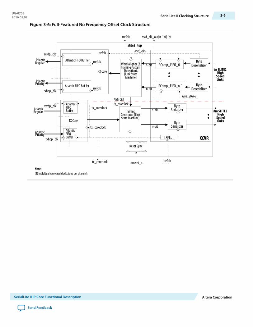
Figure 3-6: Full-Featured No Frequency Offset Clock Structure
slite2_top
XCVR
TX Coren-bit
n-bit
RX Core
n-bit
Atlantic
#n SLITE2High
SpeedLinks
#m SLITE2High
SpeedLinks
Atlantic
Atlantic
Atlantic
Regular
Priority
Priority
Regular
PComp_FIFO_0
ByteSerializer
PComp_FIFO_n-1
ByteDeserializer
ByteDeserializer
n-bit
rxrdp_clk
rxhpp_clk
txhpp_clk
txrdp_clk
rcvd_clk0
rcvd_clkn-1
tx_coreclockRREFCLK
mreset_n
Reset Sync
tx_coreclock
rcvd_clk_out[n-1:0] (1)
Atlantic FIFO Buf fer
Atlantic FIFO Buf fer
Atlantic FIFOBuffer
Atlantic FIFOBuffer
rrefclk
rrefclk
rrefclk
Word Aligner (&Training Pattern
Detection),[Link StateMachine]
TrainingGene rator [LinkState Machine]
trefclk
TXPLL
tx_coreclock
tx_coreclock
rrefclk
Note:(1) Individual recovered clocks (one per channel).
ByteSerializer
UG-07052016.05.02 SerialLite II Clocking Structure 3-9
SerialLite II IP Core Functional Description Altera Corporation
Send Feedback
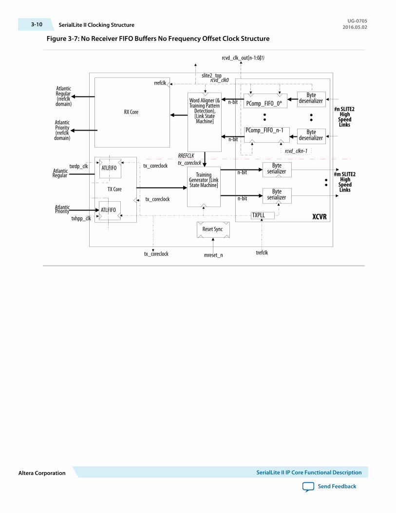
Figure 3-7: No Receiver FIFO Buffers No Frequency Offset Clock Structure
slite2_top
XCVR
TX Coren-bit
n-bit
RX Core
n-bit
#n SLITE2High
SpeedLinks
#m SLITE2High
SpeedLinks
Atlantic
AtlanticPriority
Regular
PComp_FIFO_0*
Byteserializer
Byteserializer
PComp_FIFO_n-1
Bytedeserializer
Bytedeserializer
n-bit
txhpp_clk
txrdp_clk
rcvd_clk0
rcvd_clkn-1
tx_coreclockRREFCLK
mreset_n
Reset Sync
tx_coreclock
rcvd_clk_out[n-1:0]
ATLFIFO
ATLFIFO
rrefclk
Word Aligner (&Training Pattern
Detection),[Link StateMachine]
TrainingGenerator [LinkState Machine]
AtlanticRegular(rrefclk
domain)
AtlanticPriority(rrefclk
domain)
trefclk
TXPLL
tx_coreclock
tx_coreclock
(1)
3-10 SerialLite II Clocking StructureUG-0705
2016.05.02
Altera Corporation SerialLite II IP Core Functional Description
Send Feedback
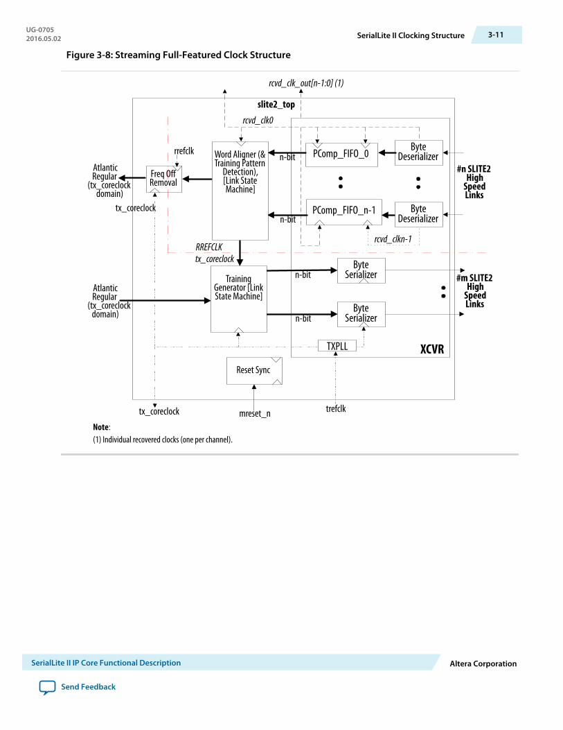
Figure 3-8: Streaming Full-Featured Clock Structure
slite2_top
XCVR
n-bit
n-bit
n-bit
#n SLITE2High
SpeedLinks
#m SLITE2High
SpeedLinks
PComp_FIFO_0
ByteSerializer
ByteSerializer
PComp_FIFO_n-1
ByteDeserializer
ByteDeserializer
n-bit
rcvd_clk0
rcvd_clkn-1
tx_coreclockRREFCLK
mreset_n
Reset Sync
tx_coreclock
rcvd_clk_out[n-1:0] (1)
Word Aligner (&Training Pattern
Detection),[Link StateMachine]
TrainingGenerator [LinkState Machine]
AtlanticRegular
(tx_coreclockdomain)
AtlanticRegular
(tx_coreclockdomain)
Freq OffRemoval
rrefclk
trefclk
TXPLL
tx_coreclock
Note:(1) Individual recovered clocks (one per channel).
UG-07052016.05.02 SerialLite II Clocking Structure 3-11
SerialLite II IP Core Functional Description Altera Corporation
Send Feedback

Figure 3-9: Streaming No Frequency Offset Clock Structure
slite2_top
XCVR
n-bit
n-bit
n-bit
#n SLITE2High
SpeedLinks
#m SLITE2High
SpeedLinks
PComp_FIFO_0
ByteSerializer
Byte
PComp_FIFO_n-1
ByteDeserializer
ByteDeserializer
n-bit
rcvd_clk0
rcvd_clkn-1
tx_coreclockRREFCLK
mreset_n
Reset Sync
tx_coreclock
rcvd_clk_out[n-1:0] (1)
Note:(1) Individual recovered clocks (one per channel).
Word Aligner (&Training Pattern
Detection),[Link StateMachine]
TrainingGene rator [LinkState Machine]
AtlanticRegular(rrefclk
domain)
AtlanticRegular
(tx_coreclockdomain)
trefclk
TXPLL
rrefclk
Serializer
3-12 SerialLite II Clocking StructureUG-0705
2016.05.02
Altera Corporation SerialLite II IP Core Functional Description
Send Feedback

Figure 3-10: Full Featured Clock Structure for 5G Symmetrical With TSIZE = 2
XCVR
TX Core
n-bit
n-bit
RX Core
n-bit
Atlantic
#n SLITE2High
Speed Links
#m SLITE2High
Speed Links
Atlantic
Atlantic
Atlantic
Re gular
Priority
Priority
Re gular
PC omp_FIFO_0
By teSerializer
By teSerializer
PC omp_ FI FO _n-1
ByteDeserializer
n-bit
rxrdp_clk
rxhpp_clk
txhpp_clk
txrdp_clk
tx_corec lk
rcvd_clkn-1
mreset_n
Rese t Sy nc
tx_coreclock
rcvd_clk_out[n-1:0]
ATLFIF O
ATLFIF O
AT LF IF O
ATLFIF O
tx_corec lock
Word Aligner (& Tr aining Pa ttern
Detection),[Link St ate Machine]
Tr aining Ge nerator [Link State Machine]
trefclk
TX PL L
tx_corec lock
tx_coreclock
tx_corec lock
tx_corec lock
RM _FIFO_0
RM_ FIFO_n-1
slite2_top
ByteDeserializer
For Arria 10, Arria V, Cyclone V, and Stratix V configurations, you must integrate the transceiver to theSerialLite II IP core manually. When you configure the transceiver to work in more than 1 lane perSerialLite II instance, the tx_clkout(0) signal from the TX channel (PHY IP) must drive the SerialLite IIinput clock (tx_coreclk) and the input port (tx_coreclkin) of all TX channels (PHY IP). Similarly, ifyour design requires more than 1 RX channel per SerialLite II instance, the rx_clkout(0) from the RXchannel (PHY IP) must drive the SerialLite II input clock (rx_coreclk) and the input port (rx_coreclkin)of all RX channels (PHY IP).
SerialLite II Pin-Out DiagramsYour SerialLite II IP core design always contains a PHY layer, based on the device you select.
The link layer portions is present if you set the Data Type option to Packets. The inclusion of receiverand transmitter components is determined by the Port Type option that you select: Bidirectional,Transmitter only, or Receiver only.
The following figures show some examples of pin-out diagrams.
UG-07052016.05.02 SerialLite II Pin-Out Diagrams 3-13
SerialLite II IP Core Functional Description Altera Corporation
Send Feedback

Figure 3-11: Arria II GX/Stratix IV PHY Layer
slite2_top
mreset_n reset_syncer
reset_logic_gx
slite2_phy
rx_clkout[0]
tx_coreclock
xcvr2OR
xcvr2_tx/xcvr2_rx
trefclk
txout[0]
txout[n]
rxin[0]
rxin[n]
TXPLL
stat_tc_pll_locked
RXPLL
err_rr_8berrdeterr_rr_disperr_rr_rlvstat_rr_sigdetstat_rr_rxlockedstat_rr_freqlockstat_rr_pattdet
ctrl_tc_serial_lpbena
stat_rr_gxsynctxrdp_enatxrdp_davtxrdp_dat
AtlanticInterface
rxrdp_datAtlantic
Interfacerxrdp_ena
tx_coreclock
rrefclkstat_rr_link
ctrl_rr_enadscram
ctrl_tc_enascram ctrl_tc_force_train
rcvd_clk_out
stat_tc_rst_done
err_rr_pol_rev_required
err_rr_dskfifo_oflw
stat_rr_dskw_done_bc
cal_blk_clkreconfig_clkreconfig_togxbreconfig_fromgxb
err_rr_pcfifo_uflwerr_rr_pcfifo_oflwerr_tc_pcfifo_oflwerr_tc_pcfifo_uflw
err_rr_foffre_oflw
stat_tc_foffre_empty
gxb_powerdown
3-14 SerialLite II Pin-Out DiagramsUG-0705
2016.05.02
Altera Corporation SerialLite II IP Core Functional Description
Send Feedback
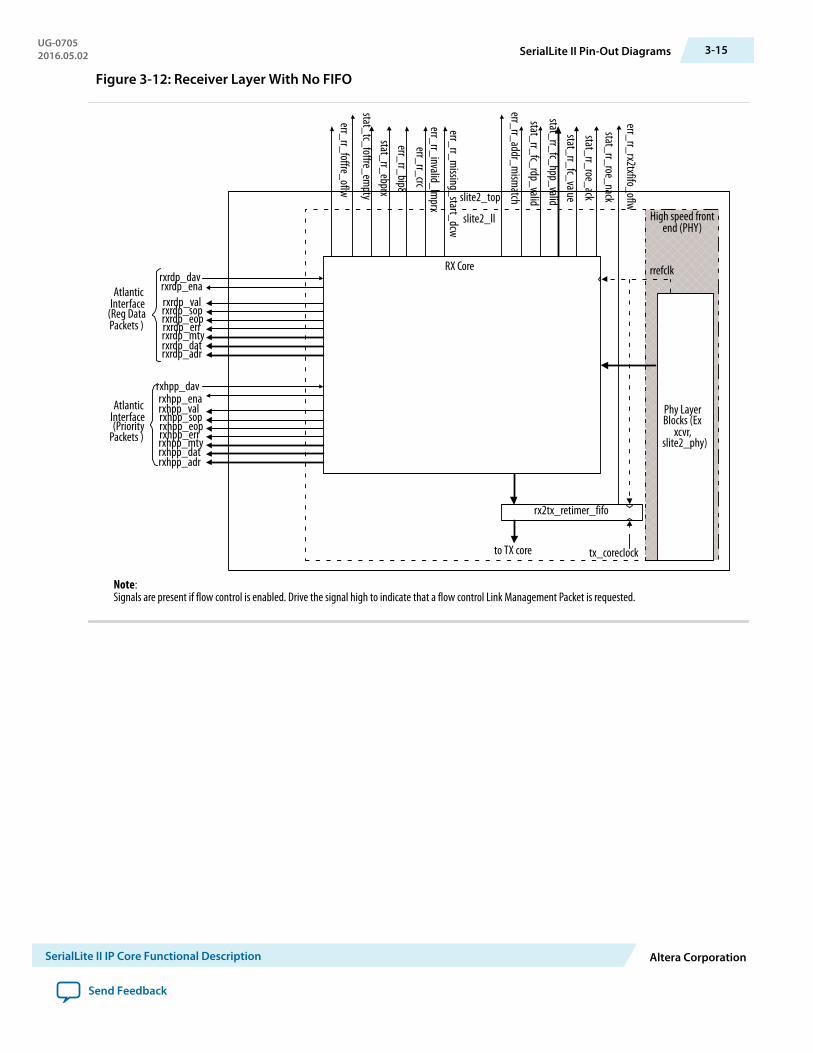
Figure 3-12: Receiver Layer With No FIFO
slite2_top
High speed frontend (PHY)
slite2_ll
RX Core
Note:Signals are present if flow control is enabled. Drive the signal high to indicate that a flow control Link Management Packet is requested.
rxrdp_enarxrdp_dav
rxrdp_soprxrdp_eoprxrdp_errrxrdp_mtyrxrdp_datrxrdp_adr
AtlanticInterface
(Reg DataPackets )
Phy LayerBlocks (Ex
xcvr,slite2_phy)
rxrdp_val
rxhpp_enarxhpp_dav
rxhpp_soprxhpp_eoprxhpp_errrxhpp_mtyrxhpp_datrxhpp_adr
AtlanticInterface(Priority
Packets )
rxhpp_val
rrefclk
tx_coreclock
err_rr_foffre_oflw
stat_tc_foffre_empty
stat_rr_ebprxerr_rr_bip8err_rr_crc
err_rr_invalid_lmprx
err_rr_missing_start_dcw
err_rr_addr_mism
atch
err_rr_rx2txfifo_oflw
stat_rr_fc_rdp_valid
stat_rr_fc_hpp_validstat_rr_fc_valuestat_rr_roe_ack
stat_rr_roe_nack
rx2tx_retimer_fifo
to TX core
UG-07052016.05.02 SerialLite II Pin-Out Diagrams 3-15
SerialLite II IP Core Functional Description Altera Corporation
Send Feedback

Figure 3-13: Receiver Link Layer With FIFO
slite2_topHigh speed front
end (PHY)slite2_ll
RX Core
Regular DataPort Atlantic
FIFO(rxrdp_atltop)
rxrdp_enarxrdp_dav
rxrdp_soprxrdp_eoprxrdp_errrxrdp_mtyrxrdp_datrxrdp_adr
AtlanticInterface
(Reg DataPackets )
rxrdp_clk
ctrl_rr_rdp_fcthresh
Phy LayerBlocks (Ex
xcvr,slite2_phy)
rxrdp_val
High PriorityPort Atlantic
FIFO(rxhpp_atltop)
rxhpp_enarxhpp_davrxhpp_soprxhpp_eoprxhpp_errrxhpp_mtyrxhpp_datrxhpp_adr
AtlanticInterface(Priority
Packets )
rxhpp_clk
ctrl_rr_hpp_fcthresh
stat_rxhpp_empty
rxhpp_val
rrefclk
tx_coreclock
ctl_rxhpp_ftl
ctl_rxhpp_eopdav
stat_rxrdp_emptyctl_rxrdp_ftl
ctl_rxrdp_eopdav
err_tc/rr_rxrdp_oflw
err_tc/rr_rxhpp_oflw
err_rr_foffre_oflw
stat_tc_foffre_empty
stat_rr_ebprxerr_rr_bip8err_rr_crc
err_rr_invalid_lmprx
err_rr_missing_start_dcw
err_rr_addr_mism
atch
err_rr_rx2txfifo_oflw
stat_rr_fc_rdp_valid
stat_rr_fc_hpp_validstat_rr_fc_valuestat_rr_roe_ack
stat_rr_roe_nack
rx2tx_retimer_fifo
To TX Core
3-16 SerialLite II Pin-Out DiagramsUG-0705
2016.05.02
Altera Corporation SerialLite II IP Core Functional Description
Send Feedback
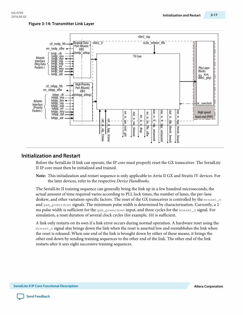
Figure 3-14: Transmitter Link Layer
slite2_top
High speedfront end (PHY)
slite2_ll
TX Core
Phy LayerBlocks (Ex xcvr,slite2_phy)
ctrl_tc_rdp_fctime
Regular DataPort Atlantic
FIFO(txrdp_atltop
)txrdp_enatxrdp_davtxrdp_soptxrdp_eoptxrdp_errtxrdp_mtytxrdp_dattxrdp_adr
txrdp_clk
ctl_txrdp_fth
AtlanticInterface(Reg DataPackets )
High PriorityPort Atlantic
FIFO(txhpp_atltop)
err_txhpp_oflwctl_txhpp_fth
tx_coreclock
txhpp_enatxhpp_davtxhpp_soptxhpp_eoptxhpp_errtxhpp_mtytxhpp_dattxhpp_adr
txhpp_clk
AtlanticInterface(Priority
Packets )
ctrl_tc_hpp_fctime
err_txrdp_oflw
err_tc_roe_rsnd_gt4
stat_tc_roe_timeout
err_tc_is_drop
err_tc_lm_fifo_oflw
stat_tc_fc_rdp_retransmit
stat_tc_fc_hpp_retransmit
stat_tc_rdp_thresh_breach
stat_tc_hpp_thresh_breach
rx2tx_retimer_fifo
Initialization and RestartBefore the SerialLite II link can operate, the IP core must properly reset the GX transceiver. The SerialLiteII IP core must then be initialized and trained.
Note: This initialization and restart sequence is only applicable to Arria II GX and Stratix IV devices. Forthe later devices, refer to the respective Device Handbooks.
The SerialLite II training sequence can generally bring the link up in a few hundred microseconds; theactual amount of time required varies according to PLL lock times, the number of lanes, the per-lanedeskew, and other variation-specific factors. The reset of the GX transceiver is controlled by the mreset_nand gxb_powerdown signals. The minimum pulse width is determined by characterization. Currently, a 2ms pulse width is sufficient for the gxb_powerdown input, and three cycles for the mreset_n signal. Forsimulation, a reset duration of several clock cycles (for example, 10) is sufficient.
A link only restarts on its own if a link error occurs during normal operation. A hardware reset using themreset_n signal also brings down the link when the reset is asserted low and reestablishes the link whenthe reset is released. When one end of the link is brought down by either of these means, it brings theother end down by sending training sequences to the other end of the link. The other end of the linkrestarts after it sees eight successive training sequences.
UG-07052016.05.02 Initialization and Restart 3-17
SerialLite II IP Core Functional Description Altera Corporation
Send Feedback

Figure 3-15: Initialization
This figure shows what happens when you initialize the SerialLite II IP core.
mreset_n
stat_tc_pll_locked
stat_rr_freqlock
stat_tc_rst_done
stat_rr_link
When the reset_n input signal is asserted, the transceiver and the IP core start to reset and initialize theIP core. When the corresponding signals, stat_tc_pll_locked, stat_rr_freqlock, and thestat_tc_rst_done signal go high, a set of training sequence are transmitted across the link to align thecharacters and lanes. When everything is synchronized, the link is established and ready to be used,stat_rr_link = 1.
Multiple Core ConfigurationWhen you instantiate multiple SerialLite II IP cores, you must apply additional guidelines to create aworking design.
• If you use the Tcl constraints to make assignments for the MegaCore functions, you must edit the Tclscript associated with each generated SerialLite II MegaCore function to update the hierarchical pathsto each clock node and signal inside the TCL scripts. You can use the generated scripts as a guide. Youmust also make these changes to the generated Synopsys Design Constraints File (.sdc) if you intend touse the TimeQuest Timing Analyzer.
Note: The Tcl scripts assume a top-level name for several clocks, such as: trefclk, rxrdp_clk,rxhpp_clk, txrdp_clk, and txhpp_clk. You must edit Set Clock Names in the scripts if theclock name connected to these inputs does not match. If the multiple cores are connected to thesame clocks at the top-level file, you must make sure Set Clock Names and clock settings areonly available in one script. You must always set to run this script first in the projects. You mustedit the Tcl script and the .sdc file if you plan to use the TimeQuest timing analyzer.
• For Arria II GX and Stratix IV designs, you must ensure that the cal_blk_clk input to each SerialLiteII IP core is driven by the same calibration clock source. Also ensure that the SerialLite II IP core andother IP core variants in the system that use the ALTGX IP core have the same clock source connectedto their respective cal_blk_clk ports.
• In Arria II GX and Stratix IV designs that include multiple SerialLite II cores in a single transceiverblock, the same signal must drive gxb_powerdown to each of the SerialLite II IP core variants.
3-18 Multiple Core ConfigurationUG-0705
2016.05.02
Altera Corporation SerialLite II IP Core Functional Description
Send Feedback
IP Core Configuration for Arria 10, Arria V, Cyclone V, and Stratix VDevices
The supported features for the SerialLite II IP core in ,Arria 10, Arria V, Cyclone V, and Stratix V devicesare the same with the Stratix IV GX devices, except for the hard transceiver features. Because there is nohard transceiver in this configuration, you need to instantiate the Custom PHY IP core and integrate bothcores in your design.
Table 3-2: Custom PHY IP Core Blocks and Data Rate Used by SerialLite II IP Core
FPGA FabricTransceiver
Interface Width
Blocks Enabled Data Rate (Mbps)for Arria 10/ Arria V
GZ/ Arria V GX/Stratix V
Data Rate (Mbps) for CycloneV
32
(TSIZE = 4)
• Word alignment mode: Manual (2)/Automatic synchronization statemachine (3)
• Word alignment pattern: 10'h17c
3,126 to 6,375 (orhigher for Arria 10devices)
3,126 to 5,000
8B/10B encoder/decoder
16
(TSIZE = 2)
• Word alignment mode: Automaticsynchronization state machine
• Word alignment pattern: 10'h17c 1,000 to 5,000 1,000 to 3,750
8B/10B encoder/decoder
8
(TSIZE = 1)
• Word alignment mode: Automaticsynchronization state machine
• Word alignment pattern: 10'h17c 622 to 2,500 622 to 1,875
8B/10B encoder/decode
Design ConsiderationWhen you instantiate the SerialLite II IP core and Custom PHY IP core, you must adhere to theseconsiderations to create a working design.
(2) Assert the rx_enapatternalign register in Custom PHY through the Avalon-MM interface to triggeranother alignment when synchronization is lost.
(3) Applicable only for Arria 10, Arria V GZ, and Stratix V devices.
UG-07052016.05.02 IP Core Configuration for Arria 10, Arria V, Cyclone V, and Stratix V... 3-19
SerialLite II IP Core Functional Description Altera Corporation
Send Feedback
Table 3-3: Design Consideration
Considerations Description
Compilation If you use Tcl constraints to make assignments for the SerialLite II IPcore, you must perform the following actions:
• Identify the Custom PHY IP core clock node.• Set the Custom PHY IP core reference clock frequency accordingly
in the .sdc file for design integration between the SerialLite II IPcore and Custom PHY IP core.
Testbench For the SISTER IP core instance, you are required to edit the SerialLiteII IP core dynamically generated testbench to include the Custom PHYIP core instantiation.
The testbench verifies whether the integration of both cores isfunctionally correct in the simulation.
Note: The SISTER IP core is a SerialLite II IP core withparameters derived from the DUT parameters.
Simulation Support The Quartus Prime software generates the simgen netlist, whichcontains only the SerialLite II IP core soft logic. The hard transceiverinstantiation logic is not included.
You are required to add the Custom PHY IP core simulation files intothe command line Tcl file (<top level design name>_run_modelsim.tcl)to enable the simulation to work in the ModelSim simulator.
Related InformationTestbench Specifications on page 4-2
Parameter Settings For SerialLite II and Custom PHY IP CoresThe parameters associated with the transceiver configuration in the SerialLite II IP core are disabledbecause there is no hard transceiver in this configuration. Other parameters for the SerialLite II IP coreremains the same and are enabled.
Refer to SerialLite II Parameter Settings on page 2-6 for a more detailed description of the parameters.
Table 3-4: Custom PHY IP Core Settings
This table lists the options that you can set using the Custom PHY IP core parameter editor. Note that therequired ports are essential for the Custom PHY IP core instantiation.
Option Description Setting
pll_locked outputport
Provides Tx PLL locking status in the CustomPHY IP core.
Optional
tx_ready outputport
Indicates that the Custom PHY IP core is readyto transmit data.
Required
rx_ready outputport
Indicates that the Custom PHY IP core is readyto receive data.
Required
3-20 Parameter Settings For SerialLite II and Custom PHY IP CoresUG-0705
2016.05.02
Altera Corporation SerialLite II IP Core Functional Description
Send Feedback
Option Description Setting
Enable TX Bitslip Provides control for bitslip functionality. OffCreate rx_coreclkinport
Provides transceiver clock output to the rx_coreclk signal in the SerialLite II IP core. ForArria 10, Arria V, Cyclone V, and Stratix Vdesigns with more than 1 channel, connecttransceiver PHY rx_clkout(0) to rx_coreclkin(N-1:0).
Required
Create tx_coreclkinport
Provides transceiver clock output to the tx_coreclk signal in the SerialLite II IP core. ForArria V, Cyclone V, and Stratix V designs withmore than 1 channel, connect transceiver PHYtx_clkout(0) to tx_coreclkin (N-1:0).
Required
Create rx_recovered_clk port
Provides a recovered clock output for thetransceiver.
Off
Create ports Provide the following ports:
• rx_is_lockedtoref
• rx_is_lockedtodata
• rx_signaldetect
• tx_forceelecidle
Optional
Avalon datainterfaces
Enables support for Avalon-Streaming (ST)interface.
Optional
Enable embeddedreset controller
Enables the controller to reset the transceiver. Required
Create word alignerstatus ports
Provide the following ports:
• rx_syncstatus
• rx_patterndetect
• rx_bitslipboundaryselectout
Required
Enable run lengthviolation checking
Enables run length violation check to the err_rr_rlv signal in the SerialLite II IP core.
Note: The err_rr_rlv signal is no longerexposed at the top level in the SerialLiteII IP core for Arria 10, Arria V, CycloneV, and Stratix V devices. Enable andmonitor this signal from the transceiver.
Required
Enable rate matchFIFO
Enables support for rate match FIFO. Optional
Create optional ratematch FIFO statusports
Enable the status ports for rate match FIFO. Optional
UG-07052016.05.02 Parameter Settings For SerialLite II and Custom PHY IP Cores 3-21
SerialLite II IP Core Functional Description Altera Corporation
Send Feedback
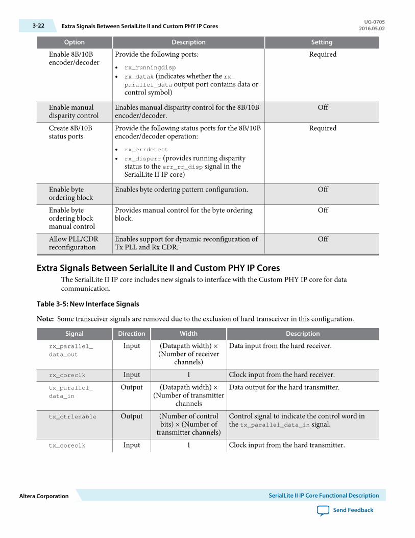
Option Description Setting
Enable 8B/10Bencoder/decoder
Provide the following ports:
• rx_runningdisp
• rx_datak (indicates whether the rx_parallel_data output port contains data orcontrol symbol)
Required
Enable manualdisparity control
Enables manual disparity control for the 8B/10Bencoder/decoder.
Off
Create 8B/10Bstatus ports
Provide the following status ports for the 8B/10Bencoder/decoder operation:
• rx_errdetect
• rx_disperr (provides running disparitystatus to the err_rr_disp signal in theSerialLite II IP core)
Required
Enable byteordering block
Enables byte ordering pattern configuration. Off
Enable byteordering blockmanual control
Provides manual control for the byte orderingblock.
Off
Allow PLL/CDRreconfiguration
Enables support for dynamic reconfiguration ofTx PLL and Rx CDR.
Off
Extra Signals Between SerialLite II and Custom PHY IP CoresThe SerialLite II IP core includes new signals to interface with the Custom PHY IP core for datacommunication.
Table 3-5: New Interface Signals
Note: Some transceiver signals are removed due to the exclusion of hard transceiver in this configuration.
Signal Direction Width Description
rx_parallel_
data_out
Input (Datapath width) ×(Number of receiver
channels)
Data input from the hard receiver.
rx_coreclk Input 1 Clock input from the hard receiver.tx_parallel_
data_in
Output (Datapath width) ×(Number of transmitter
channels
Data output for the hard transmitter.
tx_ctrlenable Output (Number of controlbits) × (Number of
transmitter channels)
Control signal to indicate the control word inthe tx_parallel_data_in signal.
tx_coreclk Input 1 Clock input from the hard transmitter.
3-22 Extra Signals Between SerialLite II and Custom PHY IP CoresUG-0705
2016.05.02
Altera Corporation SerialLite II IP Core Functional Description
Send Feedback
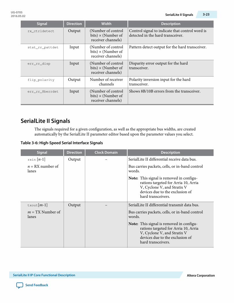
Signal Direction Width Description
rx_ctrldetect Output (Number of controlbits) × (Number ofreceiver channels)
Control signal to indicate that control word isdetected in the hard transceiver.
stat_rr_pattdet Input (Number of controlbits) × (Number ofreceiver channels)
Pattern detect output for the hard transceiver.
err_rr_disp Input (Number of controlbits) × (Number ofreceiver channels)
Disparity error output for the hardtransceiver.
flip_polarity Output Number of receiverchannels
Polarity inversion input for the hardtransceiver.
err_rr_8berrdet Input (Number of controlbits) × (Number ofreceiver channels)
Shows 8B/10B errors from the transceiver.
SerialLite II SignalsThe signals required for a given configuration, as well as the appropriate bus widths, are createdautomatically by the SerialLite II parameter editor based upon the parameter values you select.
Table 3-6: High-Speed Serial Interface Signals
Signal Direction Clock Domain Description
rxin [n-1]
n = RX number oflanes
Output – SerialLite II differential receive data bus.
Bus carries packets, cells, or in-band controlwords.
Note: This signal is removed in configu‐rations targeted for Arria 10, ArriaV, Cyclone V, and Stratix Vdevices due to the exclusion ofhard transceivers.
txout[m-1]
m = TX Number oflanes
Output – SerialLite II differential transmit data bus.
Bus carries packets, cells, or in-band controlwords.
Note: This signal is removed in configu‐rations targeted for Arria 10, ArriaV, Cyclone V, and Stratix Vdevices due to the exclusion ofhard transceivers.
UG-07052016.05.02 SerialLite II Signals 3-23
SerialLite II IP Core Functional Description Altera Corporation
Send Feedback
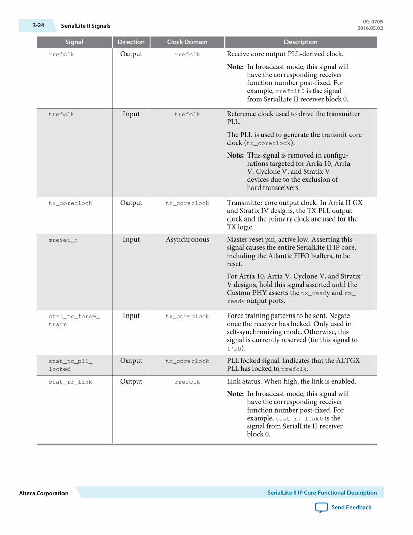
Signal Direction Clock Domain Description
rrefclk Output rrefclk Receive core output PLL-derived clock.
Note: In broadcast mode, this signal willhave the corresponding receiverfunction number post-fixed. Forexample, rrefclk0 is the signalfrom SerialLite II receiver block 0.
trefclk Input trefclk Reference clock used to drive the transmitterPLL.
The PLL is used to generate the transmit coreclock (tx_coreclock).
Note: This signal is removed in configu‐rations targeted for Arria 10, ArriaV, Cyclone V, and Stratix Vdevices due to the exclusion ofhard transceivers.
tx_coreclock Output tx_coreclock Transmitter core output clock. In Arria II GXand Stratix IV designs, the TX PLL outputclock and the primary clock are used for theTX logic.
mreset_n Input Asynchronous Master reset pin, active low. Asserting thissignal causes the entire SerialLite II IP core,including the Atlantic FIFO buffers, to bereset.
For Arria 10, Arria V, Cyclone V, and StratixV designs, hold this signal asserted until theCustom PHY asserts the tx_ready and rx_ready output ports.
ctrl_tc_force_
train
Input tx_coreclock Force training patterns to be sent. Negateonce the receiver has locked. Only used inself-synchronizing mode. Otherwise, thissignal is currently reserved (tie this signal to1'b0).
stat_tc_pll_
locked
Output tx_coreclock PLL locked signal. Indicates that the ALTGXPLL has locked to trefclk.
stat_rr_link Output rrefclk Link Status. When high, the link is enabled.
Note: In broadcast mode, this signal willhave the corresponding receiverfunction number post-fixed. Forexample, stat_rr_link0 is thesignal from SerialLite II receiverblock 0.
3-24 SerialLite II SignalsUG-0705
2016.05.02
Altera Corporation SerialLite II IP Core Functional Description
Send Feedback
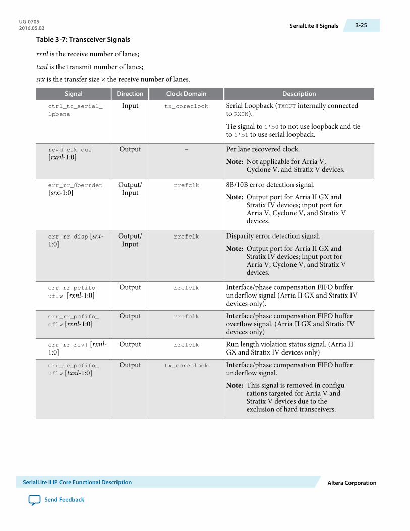
Table 3-7: Transceiver Signals
rxnl is the receive number of lanes;
txnl is the transmit number of lanes;
srx is the transfer size × the receive number of lanes.
Signal Direction Clock Domain Description
ctrl_tc_serial_
lpbena
Input tx_coreclock Serial Loopback (TXOUT internally connectedto RXIN).
Tie signal to 1'b0 to not use loopback and tieto 1'b1 to use serial loopback.
rcvd_clk_out
[rxnl-1:0]Output – Per lane recovered clock.
Note: Not applicable for Arria V,Cyclone V, and Stratix V devices.
err_rr_8berrdet
[srx-1:0]Output/
Inputrrefclk 8B/10B error detection signal.
Note: Output port for Arria II GX andStratix IV devices; input port forArria V, Cyclone V, and Stratix Vdevices.
err_rr_disp [srx-1:0]
Output/Input
rrefclk Disparity error detection signal.
Note: Output port for Arria II GX andStratix IV devices; input port forArria V, Cyclone V, and Stratix Vdevices.
err_rr_pcfifo_
uflw [rxnl-1:0]Output rrefclk Interface/phase compensation FIFO buffer
underflow signal (Arria II GX and Stratix IVdevices only).
err_rr_pcfifo_
oflw [rxnl-1:0]Output rrefclk Interface/phase compensation FIFO buffer
overflow signal. (Arria II GX and Stratix IVdevices only)
err_rr_rlv] [rxnl-1:0]
Output rrefclk Run length violation status signal. (Arria IIGX and Stratix IV devices only)
err_tc_pcfifo_
uflw [txnl-1:0]Output tx_coreclock Interface/phase compensation FIFO buffer
underflow signal.
Note: This signal is removed in configu‐rations targeted for Arria V andStratix V devices due to theexclusion of hard transceivers.
UG-07052016.05.02 SerialLite II Signals 3-25
SerialLite II IP Core Functional Description Altera Corporation
Send Feedback

Signal Direction Clock Domain Description
err_tc_pcfifo_
oflw [txnl-1:0]Output tx_coreclock Interface/phase compensation FIFO buffer
overflow signal.
(Arria II GX and Stratix IV devices only)
Note: This signal is removed in configu‐rations targeted for Arria V andStratix V devices due to theexclusion of hard transceivers.
stat_rr_
gxsync[srx-1:0]Output rrefclk Gives the status of the pattern detector and
word aligner.
Note: This signal is removed in configu‐rations targeted for Arria V andStratix V devices due to theexclusion of hard transceivers. Ifneeded, you can use the rx_syncstatus signal generatedwhen you create optional wordaligner status port during theCustom PHY generation.
stat_rr_rxlocked
[rxnl-1:0]Output rrefclk Receiver PLL locked signal. Indicates whether
or not the receiver PLL is phase locked to theCRU reference clock. When the PLL locks todata, which happens some time after thetransceiver’s rx_freqlocked signal isasserted high, this signal has little meaningbecause it only indicates lock to the referenceclock. This signal is active high for Arria IIGX and Stratix IV devices.
Note: This signal is removed in configu‐rations targeted for Arria V andStratix V devices due to theexclusion of hard transceivers. Ifneeded, you can use the rx_is_lockedtoref signal generatedwhen you create additional portsduring the Custom PHY instantia‐tion.
3-26 SerialLite II SignalsUG-0705
2016.05.02
Altera Corporation SerialLite II IP Core Functional Description
Send Feedback

Signal Direction Clock Domain Description
stat_rr_freqlock
[rxnl-1:0]Output rrefclk Frequency locked signal from the CRU.
Indicates whether the transceiver blockreceiver channel is locked to the data mode inthe rxin port.
Note: This signal is removed in configu‐rations targeted for Arria 10, ArriaV, Cyclone V, and Stratix Vdevices due to the exclusion ofhard transceivers. If needed, youcan use the rx_is_lockedtodatasignal generated when you createadditional ports during theCustom PHY instantiation.
stat_rr_pattdet
[srx-1:0]Output/
Inputrrefclk Pattern detection signal
Note: Output port for Arria II GX andStratix IV devices; input port forArria 10, Arria V, Cyclone V, andStratix V devices.
reconfig_
fromgxb ]
Arria II GX/StratixIV GX: [recon_quad*17-1:0]
Output reconfig_clk ALTGX Reconfig from the GXB Bus. Thissignal is connected to the reconfig_fromgxbport on the altgx_reconfig module.
If you use Arria II GX or Stratix IV device,you must connect this output to the altgx_reconfig module for offset cancellation.
Note: recon_quad is the total number ofQuads being used.
If the altgx_reconfig block is not used, thesignal will not toggle (set to a fixed value) andthus is not on any clock domain. If thealtgx_reconfig block is used, this signal ison the reconfig_clk domain.
Note: This signal is removed in configu‐rations targeted for Arria 10, ArriaV, Cyclone V, and Stratix Vdevices due to the exclusion ofhard transceivers.
UG-07052016.05.02 SerialLite II Signals 3-27
SerialLite II IP Core Functional Description Altera Corporation
Send Feedback
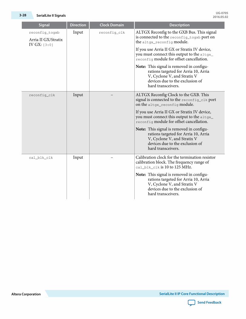
Signal Direction Clock Domain Description
reconfig_togxb
Arria II GX/StratixIV GX: [3:0]
Input reconfig_clk ALTGX Reconfig to the GXB Bus. This signalis connected to the reconfig_togxb port onthe altgx_reconfig module.
If you use Arria II GX or Stratix IV device,you must connect this output to the altgx_reconfig module for offset cancellation.
Note: This signal is removed in configu‐rations targeted for Arria 10, ArriaV, Cyclone V, and Stratix Vdevices due to the exclusion ofhard transceivers.
reconfig_clk Input – ALTGX Reconfig Clock to the GXB. Thissignal is connected to the reconfig_clk porton the altgx_reconfig module.
If you use Arria II GX or Stratix IV device,you must connect this output to the altgx_reconfig module for offset cancellation.
Note: This signal is removed in configu‐rations targeted for Arria 10, ArriaV, Cyclone V, and Stratix Vdevices due to the exclusion ofhard transceivers.
cal_blk_clk Input – Calibration clock for the termination resistorcalibration block. The frequency range ofcal_blk_clk is 10 to 125 MHz.
Note: This signal is removed in configu‐rations targeted for Arria 10, ArriaV, Cyclone V, and Stratix Vdevices due to the exclusion ofhard transceivers.
3-28 SerialLite II SignalsUG-0705
2016.05.02
Altera Corporation SerialLite II IP Core Functional Description
Send Feedback
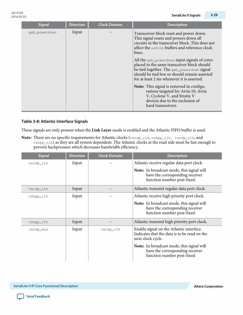
Signal Direction Clock Domain Description
gxb_powerdown Input – Transceiver block reset and power down.This signal resets and powers down allcircuits in the transceiver block. This does notaffect the refclk buffers and reference clocklines.
All the gxb_powerdown input signals of coresplaced in the same transceiver block shouldbe tied together. The gxb_powerdown signalshould be tied low or should remain assertedfor at least 2 ms whenever it is asserted.
Note: This signal is removed in configu‐rations targeted for Arria 10, ArriaV, Cyclone V, and Stratix Vdevices due to the exclusion ofhard transceivers.
Table 3-8: Atlantic Interface Signals
These signals are only present when the Link Layer mode is enabled and the Atlantic FIFO buffer is used.
Note: There are no specific requirements for Atlantic clocks (rxrdp_clk, rxhpp_clk, txrdp_clk, andtxhpp_clk) as they are all system dependent. The Atlantic clocks at the read side must be fast enough toprevent backpressure which decreases bandwidth efficiency.
Signal Direction Clock Domain Description
rxrdp_clk Input – Atlantic receive regular data port clock.
Note: In broadcast mode, this signal willhave the corresponding receiverfunction number post-fixed.
txrdp_clk Input – Atlantic transmit regular data port clock.rxhpp_clk Input – Atlantic receive high priority port clock.
Note: In broadcast mode, this signal willhave the corresponding receiverfunction number post-fixed.
txhpp_clk Input – Atlantic transmit high priority port clock.rxrdp_ena Input rxrdp_clk Enable signal on the Atlantic interface.
Indicates that the data is to be read on thenext clock cycle.
Note: In broadcast mode, this signal willhave the corresponding receiverfunction number post-fixed.
UG-07052016.05.02 SerialLite II Signals 3-29
SerialLite II IP Core Functional Description Altera Corporation
Send Feedback

Signal Direction Clock Domain Description
rxrdp_dav Input rxrdp_clk Input (No FIFO buffer) determines whetherflow control is required on this port. Whenthis signal is low, the fill level has beenbreached. When this signal is high, the FIFObuffer has enough space for more words.
Note: In broadcast mode, this signal willhave the corresponding receiverfunction number post-fixed.
rxrdp_dav Output rxrdp_clk Output (With FIFO buffer) represents thebuffer’s fill level. This signal is high when thelevel is above FTL or if an EOP is in thebuffer.
Note: In broadcast mode, this signal willhave the corresponding receiverfunction number post-fixed.
rxrdp_val Output rxrdp_clk The output data is valid.
Note: In broadcast mode, this signal willhave the corresponding receiverfunction number post-fixed.
rxrdp_sop Output rxrdp_clk Start of packet indicator on the Atlanticinterface.
Note: In broadcast mode, this signal willhave the corresponding receiverfunction number post-fixed.
rxrdp_eop Output rxrdp_clk End of packet indicator on the Atlanticinterface.
Note: In broadcast mode, this signal willhave the corresponding receiverfunction number post-fixed.
rxrdp_err Output rxrdp_clk Error indicator on the Atlantic Interface. Thissignal is not necessarily held high untilrxrdp_eop is asserted.
Note: In broadcast mode, this signal willhave the corresponding receiverfunction number post-fixed.
rxrdp_mty[m-1:0] Output rxrdp_clk Number of empty bytes in the data word.
Note: In broadcast mode, this signal willhave the corresponding receiverfunction number post-fixed.
Note: d is the empty value, which is log2(data width).
3-30 SerialLite II SignalsUG-0705
2016.05.02
Altera Corporation SerialLite II IP Core Functional Description
Send Feedback

Signal Direction Clock Domain Description
rxrdp_dat[d-1:0] Output rxrdp_clk User data bits.
Note: In broadcast mode, this signal willhave the corresponding receiverfunction number post-fixed.
Note: m is the data width, which is 8 ×transfer size × the RX number oflanes.
rxrdp_adr[7:0] Output rxrdp_clk User-defined packet ID. Only valid withrxrdp_sop.
Note: In broadcast mode, this signal willhave the corresponding receiverfunction number post-fixed.
txrdp_ena Input txrdp_clk Enable signal on the Atlantic interface.Indicates that the data is valid.
txrdp_dav Output txrdp_clk Indicates that the input FIFO buffer is notfull.
txrdp_sop Input txrdp_clk Start of packet indicator on the Atlanticinterface.
txrdp_eop Input txrdp_clk End of packet indicator on the Atlanticinterface.
txrdp_err Input txrdp_clk Error indicator on the Atlantic interface.txrdp_mty[tm-
1:0]
Input txrdp_clk Number of empty bytes in the data word.
Note: tm is the empty value, which islog2 (data width).
txrdp_dat[td-
1:0]
Input txrdp_clk User data bits.
Note: td is the data width, which is 8 ×transfer size × the TX number oflanes.
txrdp_adr[7:0] Input txrdp_clk User-defined packet ID.rxhpp_ena Input rxhpp_clk Enable signal on the Atlantic interface.
Indicates that the data is to be read on thenext clock cycle.
Note: In broadcast mode, this signal willhave the corresponding receiverfunction number post-fixed.
UG-07052016.05.02 SerialLite II Signals 3-31
SerialLite II IP Core Functional Description Altera Corporation
Send Feedback
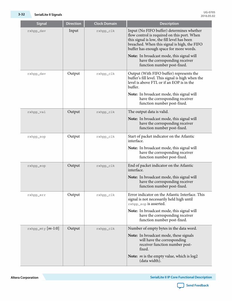
Signal Direction Clock Domain Description
rxhpp_dav Input rxhpp_clk Input (No FIFO buffer) determines whetherflow control is required on this port. Whenthis signal is low, the fill level has beenbreached. When this signal is high, the FIFObuffer has enough space for more words.
Note: In broadcast mode, this signal willhave the corresponding receiverfunction number post-fixed.
rxhpp_dav Output rxhpp_clk Output (With FIFO buffer) represents thebuffer’s fill level. This signal is high when thelevel is above FTL or if an EOP is in thebuffer.
Note: In broadcast mode, this signal willhave the corresponding receiverfunction number post-fixed.
rxhpp_val Output rxhpp_clk The output data is valid.
Note: In broadcast mode, this signal willhave the corresponding receiverfunction number post-fixed.
rxhpp_sop Output rxhpp_clk Start of packet indicator on the Atlanticinterface.
Note: In broadcast mode, this signal willhave the corresponding receiverfunction number post-fixed.
rxhpp_eop Output rxhpp_clk End of packet indicator on the Atlanticinterface.
Note: In broadcast mode, this signal willhave the corresponding receiverfunction number post-fixed.
rxhpp_err Output rxhpp_clk Error indicator on the Atlantic Interface. Thissignal is not necessarily held high untilrxhpp_eop is asserted.
Note: In broadcast mode, this signal willhave the corresponding receiverfunction number post-fixed.
rxhpp_mty [m-1:0] Output rxhpp_clk Number of empty bytes in the data word.
Note: In broadcast mode, these signalswill have the correspondingreceiver function number post-fixed.
Note: m is the empty value, which is log2(data width).
3-32 SerialLite II SignalsUG-0705
2016.05.02
Altera Corporation SerialLite II IP Core Functional Description
Send Feedback
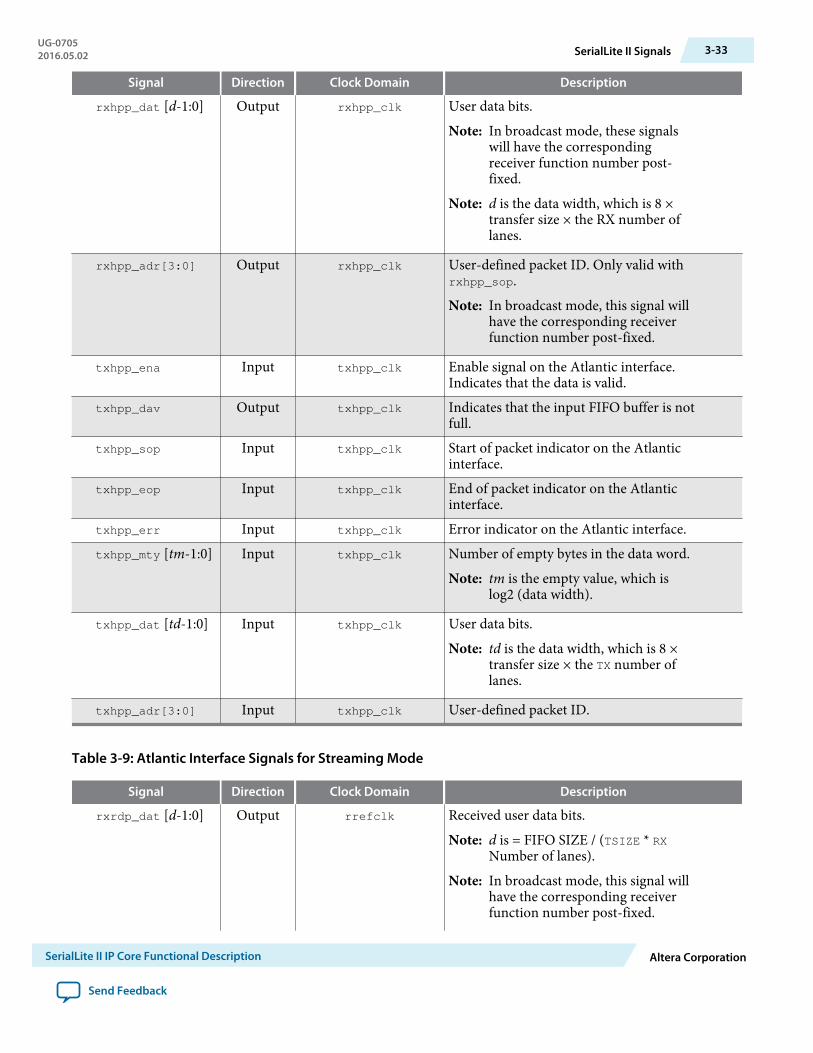
Signal Direction Clock Domain Description
rxhpp_dat [d-1:0] Output rxhpp_clk User data bits.
Note: In broadcast mode, these signalswill have the correspondingreceiver function number post-fixed.
Note: d is the data width, which is 8 ×transfer size × the RX number oflanes.
rxhpp_adr[3:0] Output rxhpp_clk User-defined packet ID. Only valid withrxhpp_sop.
Note: In broadcast mode, this signal willhave the corresponding receiverfunction number post-fixed.
txhpp_ena Input txhpp_clk Enable signal on the Atlantic interface.Indicates that the data is valid.
txhpp_dav Output txhpp_clk Indicates that the input FIFO buffer is notfull.
txhpp_sop Input txhpp_clk Start of packet indicator on the Atlanticinterface.
txhpp_eop Input txhpp_clk End of packet indicator on the Atlanticinterface.
txhpp_err Input txhpp_clk Error indicator on the Atlantic interface.txhpp_mty [tm-1:0] Input txhpp_clk Number of empty bytes in the data word.
Note: tm is the empty value, which islog2 (data width).
txhpp_dat [td-1:0] Input txhpp_clk User data bits.
Note: td is the data width, which is 8 ×transfer size × the TX number oflanes.
txhpp_adr[3:0] Input txhpp_clk User-defined packet ID.
Table 3-9: Atlantic Interface Signals for Streaming Mode
Signal Direction Clock Domain Description
rxrdp_dat [d-1:0] Output rrefclk Received user data bits.
Note: d is = FIFO SIZE / (TSIZE * RXNumber of lanes).
Note: In broadcast mode, this signal willhave the corresponding receiverfunction number post-fixed.
UG-07052016.05.02 SerialLite II Signals 3-33
SerialLite II IP Core Functional Description Altera Corporation
Send Feedback
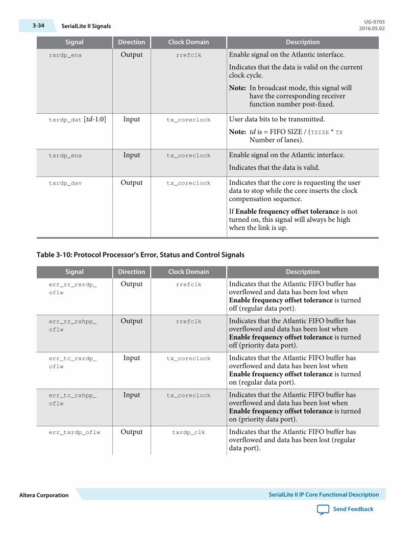
Signal Direction Clock Domain Description
rxrdp_ena Output rrefclk Enable signal on the Atlantic interface.
Indicates that the data is valid on the currentclock cycle.
Note: In broadcast mode, this signal willhave the corresponding receiverfunction number post-fixed.
txrdp_dat [td-1:0] Input tx_coreclock User data bits to be transmitted.
Note: td is = FIFO SIZE / (TSIZE * TXNumber of lanes).
txrdp_ena Input tx_coreclock Enable signal on the Atlantic interface.
Indicates that the data is valid.
txrdp_dav Output tx_coreclock Indicates that the core is requesting the userdata to stop while the core inserts the clockcompensation sequence.
If Enable frequency offset tolerance is notturned on, this signal will always be highwhen the link is up.
Table 3-10: Protocol Processor’s Error, Status and Control Signals
Signal Direction Clock Domain Description
err_rr_rxrdp_
oflw
Output rrefclk Indicates that the Atlantic FIFO buffer hasoverflowed and data has been lost whenEnable frequency offset tolerance is turnedoff (regular data port).
err_rr_rxhpp_
oflw
Output rrefclk Indicates that the Atlantic FIFO buffer hasoverflowed and data has been lost whenEnable frequency offset tolerance is turnedoff (priority data port).
err_tc_rxrdp_
oflw
Input tx_coreclock Indicates that the Atlantic FIFO buffer hasoverflowed and data has been lost whenEnable frequency offset tolerance is turnedon (regular data port).
err_tc_rxhpp_
oflw
Input tx_coreclock Indicates that the Atlantic FIFO buffer hasoverflowed and data has been lost whenEnable frequency offset tolerance is turnedon (priority data port).
err_txrdp_oflw Output txrdp_clk Indicates that the Atlantic FIFO buffer hasoverflowed and data has been lost (regulardata port).
3-34 SerialLite II SignalsUG-0705
2016.05.02
Altera Corporation SerialLite II IP Core Functional Description
Send Feedback

Signal Direction Clock Domain Description
err_txhpp_oflw txhpp_clk Indicates that the high-priority Atlantic FIFObuffer has overflowed and data has been lost.If the Retry-on-error parameter is turned on,this signal remains high until the FIFO bufferhas been emptied by the SerialLite II IP core.
stat_rxrdp_empty rxdrp_clk Indicates that the internal Atlantic FIFObuffer is empty, and the read request isignored.
Note: In broadcast mode, this signal willhave the corresponding receiverfunction number post-fixed.
stat_rxhpp_empty rxhpp_clk Indicates that the internal Atlantic FIFObuffer is empty, and the read request isignored.
Note: In broadcast mode, this signal willhave the corresponding receiverfunction number post-fixed.
ctl_rxhpp_ftl [n-1:0])
rxhpp_clk Receive high priority port FIFO threshold low(dav control). Determines when to informthe user logic that data is available via therxhpp_dav signal. This threshold applies toall buffers. Units are in elements. Onlychange at reset.
Note: n is = FIFO SIZE / (TSIZE * RXNumber of lanes).
ctl_rxrdp_ftl [n-1:0]
rxrdp_clk Receive regular data port FIFO threshold low(dav control). Determines when to informthe user logic that space is available via therxrdp_dav signal. This threshold applies toall buffers. Units are in elements. Onlychange at reset.
Note: n is = FIFO SIZE / (TSIZE * RXNumber of lanes).
ctl_rxhpp_eopdav rxhpp_clk Receive high priority port FIFO buffer end-of-packet (EOP)-based dav control. Assert toturn on dav when there is an end of packetbelow the FTL threshold. Value applies to allAtlantic buffers. Only change at reset.
Note: In broadcast mode, this signal willhave the corresponding receiverfunction number post-fixed.
UG-07052016.05.02 SerialLite II Signals 3-35
SerialLite II IP Core Functional Description Altera Corporation
Send Feedback
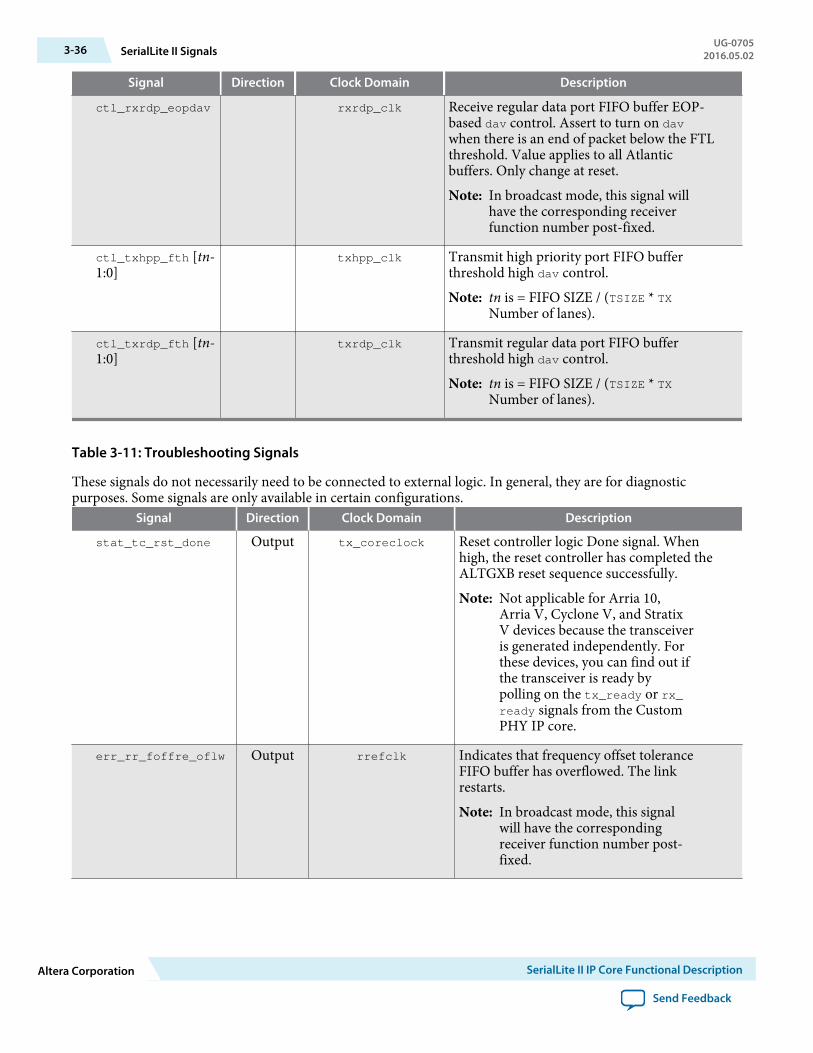
Signal Direction Clock Domain Description
ctl_rxrdp_eopdav rxrdp_clk Receive regular data port FIFO buffer EOP-based dav control. Assert to turn on davwhen there is an end of packet below the FTLthreshold. Value applies to all Atlanticbuffers. Only change at reset.
Note: In broadcast mode, this signal willhave the corresponding receiverfunction number post-fixed.
ctl_txhpp_fth [tn-1:0]
txhpp_clk Transmit high priority port FIFO bufferthreshold high dav control.
Note: tn is = FIFO SIZE / (TSIZE * TXNumber of lanes).
ctl_txrdp_fth [tn-1:0]
txrdp_clk Transmit regular data port FIFO bufferthreshold high dav control.
Note: tn is = FIFO SIZE / (TSIZE * TXNumber of lanes).
Table 3-11: Troubleshooting Signals
These signals do not necessarily need to be connected to external logic. In general, they are for diagnosticpurposes. Some signals are only available in certain configurations.
Signal Direction Clock Domain Description
stat_tc_rst_done Output tx_coreclock Reset controller logic Done signal. Whenhigh, the reset controller has completed theALTGXB reset sequence successfully.
Note: Not applicable for Arria 10,Arria V, Cyclone V, and StratixV devices because the transceiveris generated independently. Forthese devices, you can find out ifthe transceiver is ready bypolling on the tx_ready or rx_ready signals from the CustomPHY IP core.
err_rr_foffre_oflw Output rrefclk Indicates that frequency offset toleranceFIFO buffer has overflowed. The linkrestarts.
Note: In broadcast mode, this signalwill have the correspondingreceiver function number post-fixed.
3-36 SerialLite II SignalsUG-0705
2016.05.02
Altera Corporation SerialLite II IP Core Functional Description
Send Feedback
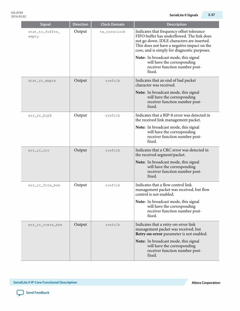
Signal Direction Clock Domain Description
stat_tc_foffre_
empty
Output tx_coreclock Indicates that frequency offset toleranceFIFO buffer has underflowed. The link doesnot go down. IDLE characters are inserted.This does not have a negative impact on thecore, and is simply for diagnostic purposes.
Note: In broadcast mode, this signalwill have the correspondingreceiver function number post-fixed.
stat_rr_ebprx Output rrefclk Indicates that an end of bad packetcharacter was received.
Note: In broadcast mode, this signalwill have the correspondingreceiver function number post-fixed.
err_rr_bip8 Output rrefclk Indicates that a BIP-8 error was detected inthe received link management packet.
Note: In broadcast mode, this signalwill have the correspondingreceiver function number post-fixed.
err_rr_crc Output rrefclk Indicates that a CRC error was detected inthe received segment/packet.
Note: In broadcast mode, this signalwill have the correspondingreceiver function number post-fixed.
err_rr_fcrx_bne Output rrefclk Indicates that a flow control linkmanagement packet was received, but flowcontrol is not enabled.
Note: In broadcast mode, this signalwill have the correspondingreceiver function number post-fixed.
err_rr_roerx_bne Output rrefclk Indicates that a retry-on-error linkmanagement packet was received, butRetry-on-error parameter is not enabled.
Note: In broadcast mode, this signalwill have the correspondingreceiver function number post-fixed.
UG-07052016.05.02 SerialLite II Signals 3-37
SerialLite II IP Core Functional Description Altera Corporation
Send Feedback
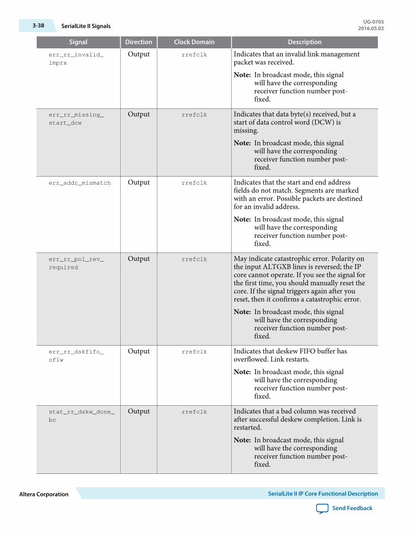
Signal Direction Clock Domain Description
err_rr_invalid_
lmprx
Output rrefclk Indicates that an invalid link managementpacket was received.
Note: In broadcast mode, this signalwill have the correspondingreceiver function number post-fixed.
err_rr_missing_
start_dcw
Output rrefclk Indicates that data byte(s) received, but astart of data control word (DCW) ismissing.
Note: In broadcast mode, this signalwill have the correspondingreceiver function number post-fixed.
err_addr_mismatch Output rrefclk Indicates that the start and end addressfields do not match. Segments are markedwith an error. Possible packets are destinedfor an invalid address.
Note: In broadcast mode, this signalwill have the correspondingreceiver function number post-fixed.
err_rr_pol_rev_
required
Output rrefclk May indicate catastrophic error. Polarity onthe input ALTGXB lines is reversed; the IPcore cannot operate. If you see the signal forthe first time, you should manually reset thecore. If the signal triggers again after youreset, then it confirms a catastrophic error.
Note: In broadcast mode, this signalwill have the correspondingreceiver function number post-fixed.
err_rr_dskfifo_
oflw
Output rrefclk Indicates that deskew FIFO buffer hasoverflowed. Link restarts.
Note: In broadcast mode, this signalwill have the correspondingreceiver function number post-fixed.
stat_rr_dskw_done_
bc
Output rrefclk Indicates that a bad column was receivedafter successful deskew completion. Link isrestarted.
Note: In broadcast mode, this signalwill have the correspondingreceiver function number post-fixed.
3-38 SerialLite II SignalsUG-0705
2016.05.02
Altera Corporation SerialLite II IP Core Functional Description
Send Feedback
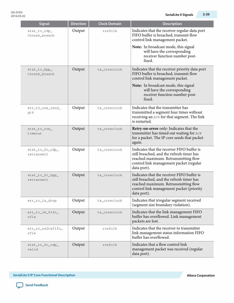
Signal Direction Clock Domain Description
stat_tc_rdp_
thresh_breach
Output rrefclk Indicates that the receiver regular data portFIFO buffer is breached, transmit flowcontrol link management packet.
Note: In broadcast mode, this signalwill have the correspondingreceiver function number post-fixed.
stat_tc_hpp_
thresh_breach
Output tx_coreclock Indicates that the receiver priority data portFIFO buffer is breached, transmit flowcontrol link management packet.
Note: In broadcast mode, this signalwill have the correspondingreceiver function number post-fixed.
err_tc_roe_rsnd_
gt4
Output tx_coreclock Indicates that the transmitter hastransmitted a segment four times withoutreceiving an ACK for that segment. The linkis restarted.
stat_tc_roe_
timeout
Output tx_coreclock Retry-on-error only: Indicates that thetransmitter has timed out waiting for ACKfor a packet. The IP core sends that packetagain.
stat_tc_fc_rdp_
retransmit
Output tx_coreclock Indicates that the receiver FIFO buffer isstill breached, and the refresh timer hasreached maximum. Retransmitting flowcontrol link management packet (regulardata port).
stat_tc_fc_hpp_
retransmit
Output tx_coreclock Indicates that the receiver FIFO buffer isstill breached, and the refresh timer hasreached maximum. Retransmitting flowcontrol link management packet (prioritydata port).
err_tc_is_drop Output tx_coreclock Indicates that irregular segment received(segment size boundary violation).
err_tc_lm_fifo_
oflw
Output tx_coreclock Indicates that the link management FIFObuffer has overflowed. Link managementpackets are lost.
err_rr_rx2txfifo_
oflw
Output rrefclk Indicates that the receiver to transmitterlink management status information FIFObuffer has overflowed.
stat_rr_fc_rdp_
valid
Output rrefclk Indicates that a flow control linkmanagement packet was received (regulardata port).
UG-07052016.05.02 SerialLite II Signals 3-39
SerialLite II IP Core Functional Description Altera Corporation
Send Feedback

Signal Direction Clock Domain Description
stat_rr_fc_hpp_
valid
Output rrefclk Indicates that a flow control linkmanagement packet was received (prioritydata port).
stat_rr_fc_
value[7:0]
Output rrefclk Indicates that the RAW FC_TIME value isembedded in the valid flow control linkmanagement packet. Decode with thestat_rr_fc_rdp_valid and stat_rr_fc_hpp_valid signals.
stat_rr_roe_ack Output rrefclk Indicates that a retry-on-error linkmanagement packet of type ACK wasreceived.
stat_rr_roe_nack Output rrefclk Indicates that a retry-on-error linkmanagement packet of type NACK wasreceived.
IP Core VerificationThe SerialLite II IP core has been rigorously tested and verified in hardware for different platforms andenvironments.
Each environment has individual test suites, that are designed to cover the following categories:
• Link initialization• Packet format• Packet priority• Flow control• Endurance• Throughput
These test suites contain several testbenches, that are grouped and focused on testing specific features ofthe SerialLite II IP core. These individual testbenches set unique parameters for each specific feature test.
3-40 IP Core VerificationUG-0705
2016.05.02
Altera Corporation SerialLite II IP Core Functional Description
Send Feedback

SerialLite II IP Core Testbench 42016.05.02
UG-0705 Subscribe Send Feedback
The SerialLite II IP core testbench helps you to verify your design implementation.
The testbench shows you how to instantiate a model in a design, it stimulates the inputs and checks theoutputs of the interfaces of the SerialLite II IP core, demonstrating basic functionality. The demonstrationtestbench is generic and you can use it with any Verilog HDL or VHDL simulator. You can run thetestbench in the standard edition (SE) or the Altera edition (AE) of the ModelSim software.
• Easy to use simulation environment for any standard Verilog HDL or VHDL simulator. For VHDLconfigurations where the VHDL demonstration testbench is not generated, a mixed languagesimulator is required to simulate the Verilog HDL testbench with the VHDL IP Functional Simulationmodels
• Open source Verilog HDL or VHDL testbench files.• Flexible SerialLite II functional model to verify your application that uses any SerialLite II IP core.• Simulates all basic SerialLite II transactions.
Note: For Arria 10, Arria V, Cyclone V, and Stratix V configurations, you are required to edit thedynamically generated testbench to include the Custom PHY IP core instantiation. You also needto update the generated <variant_name>_run_modelsim.tcl to include the Custom PHYtransceiver files.
Related InformationIP Core Configuration for Arria 10, Arria V, Cyclone V, and Stratix V Devices on page 3-19
Testbench FilesThe Quartus Prime software generates the testbench files when you create a SerialLite IP core variation.
The Verilog HDL demonstration testbench and associated scripts are generated automatically when youcreate a SerialLite II IP core variation.
The VHDL demonstration testbench and the scripts to run it are generated when you create a SerialLite IIIP core variation that meets the following criteria:
© 2016 Altera Corporation. All rights reserved. ALTERA, ARRIA, CYCLONE, ENPIRION, MAX, MEGACORE, NIOS, QUARTUS and STRATIX words and logos aretrademarks of Altera Corporation and registered in the U.S. Patent and Trademark Office and in other countries. All other words and logos identified astrademarks or service marks are the property of their respective holders as described at www.altera.com/common/legal.html. Altera warrants performanceof its semiconductor products to current specifications in accordance with Altera's standard warranty, but reserves the right to make changes to anyproducts and services at any time without notice. Altera assumes no responsibility or liability arising out of the application or use of any information,product, or service described herein except as expressly agreed to in writing by Altera. Altera customers are advised to obtain the latest version of devicespecifications before relying on any published information and before placing orders for products or services.
ISO9001:2008Registered
www.altera.com101 Innovation Drive, San Jose, CA 95134
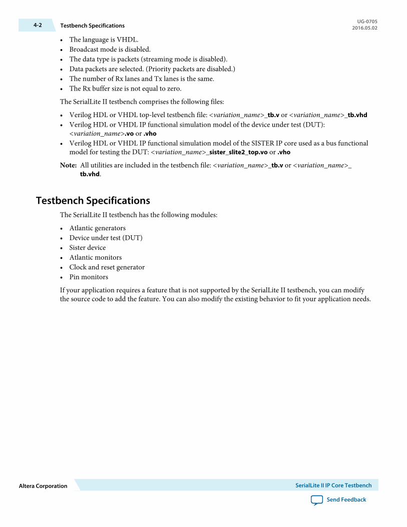
• The language is VHDL.• Broadcast mode is disabled.• The data type is packets (streaming mode is disabled).• Data packets are selected. (Priority packets are disabled.)• The number of Rx lanes and Tx lanes is the same.• The Rx buffer size is not equal to zero.
The SerialLite II testbench comprises the following files:
• Verilog HDL or VHDL top-level testbench file: <variation_name>_tb.v or <variation_name>_tb.vhd• Verilog HDL or VHDL IP functional simulation model of the device under test (DUT):
<variation_name>.vo or .vho• Verilog HDL or VHDL IP functional simulation model of the SISTER IP core used as a bus functional
model for testing the DUT: <variation_name>_sister_slite2_top.vo or .vho
Note: All utilities are included in the testbench file: <variation_name>_tb.v or <variation_name>_tb.vhd.
Testbench SpecificationsThe SerialLite II testbench has the following modules:
• Atlantic generators• Device under test (DUT)• Sister device• Atlantic monitors• Clock and reset generator• Pin monitors
If your application requires a feature that is not supported by the SerialLite II testbench, you can modifythe source code to add the feature. You can also modify the existing behavior to fit your application needs.
4-2 Testbench SpecificationsUG-0705
2016.05.02
Altera Corporation SerialLite II IP Core Testbench
Send Feedback
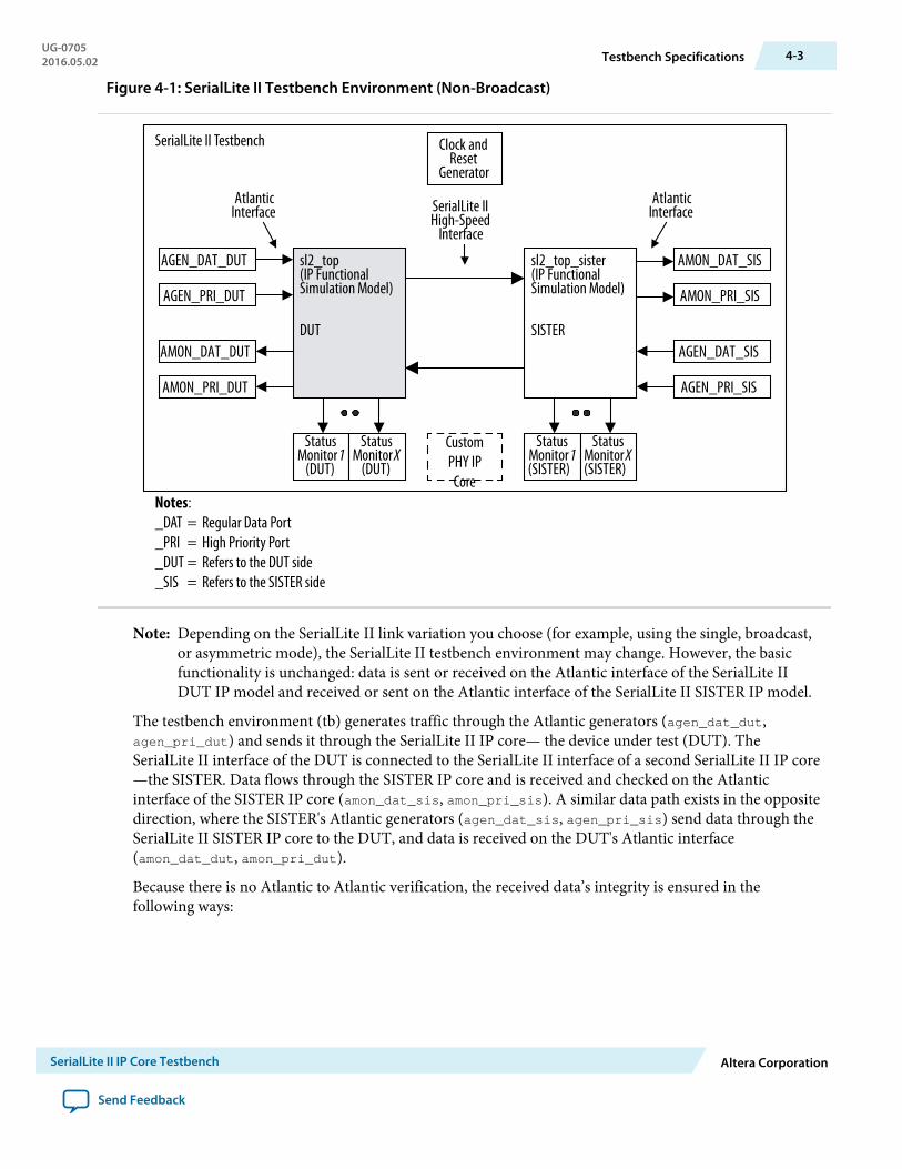
Figure 4-1: SerialLite II Testbench Environment (Non-Broadcast)
sl2_top(IP FunctionalSimulation Model)
DUT
sl2_top_sister(IP FunctionalSimulation Model)
SISTER
AGEN_DAT_DUT
StatusMonitor 1
(DUT)
Clock andReset
Generator
CustomPHY IP
Core
AtlanticInterface
AtlanticInterfaceSerialLite II
High-SpeedInterface
SerialLite II Testbench
AGEN_PRI_DUT
AMON_DAT_DUT
AMON_PRI_DUT
AMON_DAT_SIS
AMON_PRI_SIS
AGEN_DAT_SIS
AGEN_PRI_SIS
StatusMonitor X
(DUT)
StatusMonitor 1(SISTER)
StatusMonitor X(SISTER)
_DAT_PRI_DUT_SIS
Notes:= Regular Data Port= High Priority Port= Refers to the DUT side= Refers to the SISTER side
Note: Depending on the SerialLite II link variation you choose (for example, using the single, broadcast,or asymmetric mode), the SerialLite II testbench environment may change. However, the basicfunctionality is unchanged: data is sent or received on the Atlantic interface of the SerialLite IIDUT IP model and received or sent on the Atlantic interface of the SerialLite II SISTER IP model.
The testbench environment (tb) generates traffic through the Atlantic generators (agen_dat_dut,agen_pri_dut) and sends it through the SerialLite II IP core— the device under test (DUT). TheSerialLite II interface of the DUT is connected to the SerialLite II interface of a second SerialLite II IP core—the SISTER. Data flows through the SISTER IP core and is received and checked on the Atlanticinterface of the SISTER IP core (amon_dat_sis, amon_pri_sis). A similar data path exists in the oppositedirection, where the SISTER's Atlantic generators (agen_dat_sis, agen_pri_sis) send data through theSerialLite II SISTER IP core to the DUT, and data is received on the DUT's Atlantic interface(amon_dat_dut, amon_pri_dut).
Because there is no Atlantic to Atlantic verification, the received data’s integrity is ensured in thefollowing ways:
UG-07052016.05.02 Testbench Specifications 4-3
SerialLite II IP Core Testbench Altera Corporation
Send Feedback
• • Each Atlantic generator generates a certain number of packets or streaming bytes which thecorresponding Atlantic monitor receives.
• The generated data follows a pseudo-random sequence (Verilog HDL) or incrementing datasequence (VHDL) that is checked by the Atlantic monitors.
• Each packet has an incrementing identifier (first byte in the packet) that is checked by the Atlanticmonitor.
The SISTER IP core is a SerialLite II IP core with parameters derived from the DUT parameters.
• • If the DUT is symmetrical (receiver's parameters matching transmitter's parameters), the SISTER'sparameters match the DUT parameters.
• If the DUT is asymmetrical, the SISTER's parameters are different than the DUT's parameters, sothat the DUT's transmitter parameters match the SISTER's receiver parameters and vice-versa.
For a broadcast DUT, there are multiple SISTER instantiations. Pin monitor utilities monitor theSerialLite II status and error pins of the DUT and SISTER(s).
Note: The Custom PHY IP core is only applicable in configurations targeted for Arria V, Cyclone V, andStratix V devices.
Depending on the SerialLite II link variation you choose (for example, using the single, broadcast, orasymmetric mode) the SerialLite II testbench environment may change, but the basic functionality isunchanged: data is sent or received on the Atlantic interface of the SerialLite II DUT IP model andreceived or sent on the Atlantic interface of the SerialLite II SISTER IP model.
4-4 Testbench SpecificationsUG-0705
2016.05.02
Altera Corporation SerialLite II IP Core Testbench
Send Feedback

Figure 4-2: SerialLite II Testbench Environment (Single Mode–Transmitter Only, Verilog HDL Only,Non-Broadcast)
This figure shows the testbench environment for a SerialLite II single mode–transmitter only, non-broadcast mode IP core. The SISTER model contains a receiver.
sl2_top(IP FunctionalSimulation Model)
DUT
sl2_top_sister(IP FunctionalSimulation Model)
SISTER
AGEN_DAT_DUT
AtlanticInterface
AtlanticInterfaceSerialLite II
High-SpeedInterface
SerialLite II Testbench
AGEN_PRI_DUT
AMON_DAT_SIS
AMON_PRI_SIS
Clock andReset
Generator
StatusMonitor 1(SISTER)
StatusMonitor X(SISTER)
StatusMonitor 1
(DUT)
StatusMonitor X
(DUT)Custom PHY
IP Core
_DAT_PRI_DUT_SIS
Notes:= Regular Data Port= High Priority Port= Refers to the DUT side= Refers to the SISTER side
Note: The DUT and the SISTER IP cores may have different parameters; depending on the DUTparameters, and some components may be missing.
UG-07052016.05.02 Testbench Specifications 4-5
SerialLite II IP Core Testbench Altera Corporation
Send Feedback
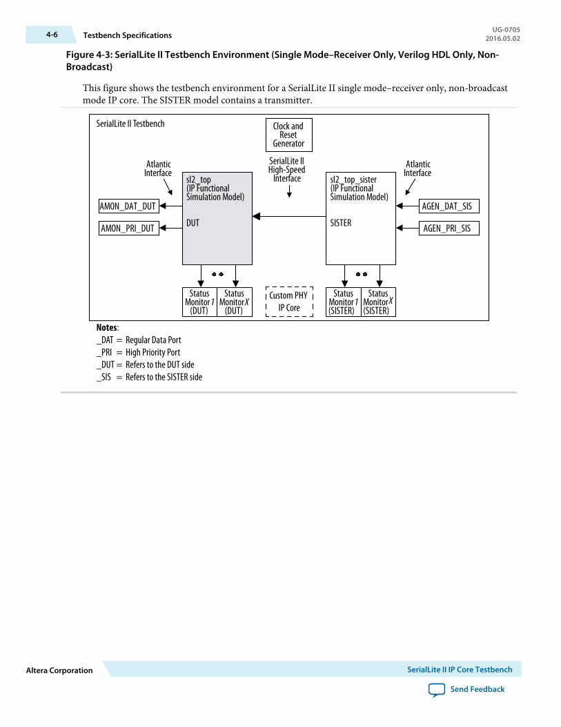
Figure 4-3: SerialLite II Testbench Environment (Single Mode–Receiver Only, Verilog HDL Only, Non-Broadcast)
This figure shows the testbench environment for a SerialLite II single mode–receiver only, non-broadcastmode IP core. The SISTER model contains a transmitter.
sl2_top(IP FunctionalSimulation Model)
DUT
sl2_top_sister(IP FunctionalSimulation Model)
SISTER
AtlanticInterface
AtlanticInterface
SerialLite IIHigh-Speed
Interface
SerialLite II Testbench
AMON_DAT_DUT
AMON_PRI_DUT
AGEN_DAT_SIS
AGEN_PRI_SIS
Clock andReset
Generator
StatusMonitor 1(SISTER)
StatusMonitor X(SISTER)
StatusMonitor 1
(DUT)
StatusMonitor X
(DUT)
_DAT_PRI_DUT_SIS
Notes:= Regular Data Port= High Priority Port= Refers to the DUT side= Refers to the SISTER side
Custom PHY IP Core
4-6 Testbench SpecificationsUG-0705
2016.05.02
Altera Corporation SerialLite II IP Core Testbench
Send Feedback
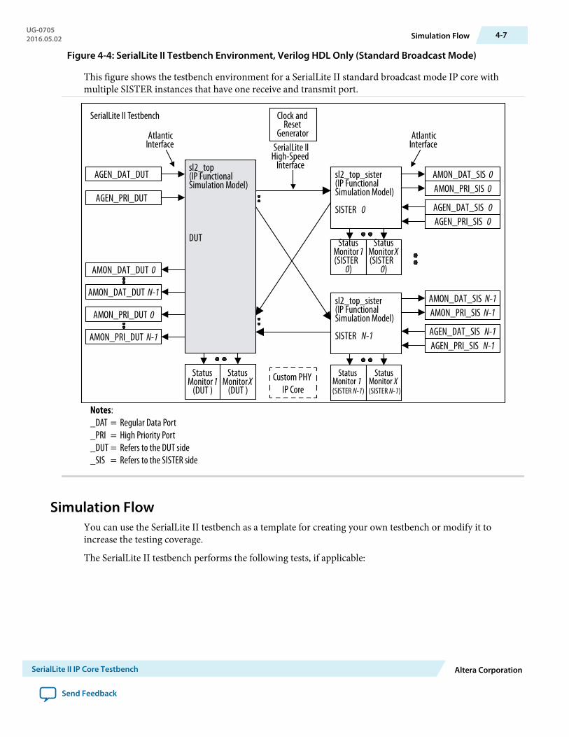
Figure 4-4: SerialLite II Testbench Environment, Verilog HDL Only (Standard Broadcast Mode)
This figure shows the testbench environment for a SerialLite II standard broadcast mode IP core withmultiple SISTER instances that have one receive and transmit port.
sl2_top(IP FunctionalSimulation Model)
DUT
sl2_top_sister(IP FunctionalSimulation Model)
SISTER 0
AtlanticInterface
AtlanticInterfaceSerialLite II
High-SpeedInterface
SerialLite II Testbench
AGEN_DAT_DUT
AGEN_PRI_DUT
AMON_DAT_DUT 0
AMON_DAT_DUT N-1
AMON_PRI_DUT N-1
AMON_PRI_DUT 0
AMON_DAT_SIS 0AMON_PRI_SIS 0
AGEN_DAT_SIS 0AGEN_PRI_SIS 0
sl2_top_sister(IP FunctionalSimulation Model)
SISTER N-1
AMON_DAT_SIS N-1AMON_PRI_SIS N-1
AGEN_DAT_SIS N-1AGEN_PRI_SIS N-1
Clock andReset
Generator
StatusMonitor 1
(SISTER N-1)
StatusMonitor 1(SISTER
0)
StatusMonitor X(SISTER
0)
StatusMonitor 1
(DUT )
StatusMonitor X
(DUT )
_DAT_PRI_DUT_SIS
Notes:= Regular Data Port= High Priority Port= Refers to the DUT side= Refers to the SISTER side
Custom PHY IP Core
StatusMonitor X
(SISTER N-1)
Simulation FlowYou can use the SerialLite II testbench as a template for creating your own testbench or modify it toincrease the testing coverage.
The SerialLite II testbench performs the following tests, if applicable:
UG-07052016.05.02 Simulation Flow 4-7
SerialLite II IP Core Testbench Altera Corporation
Send Feedback
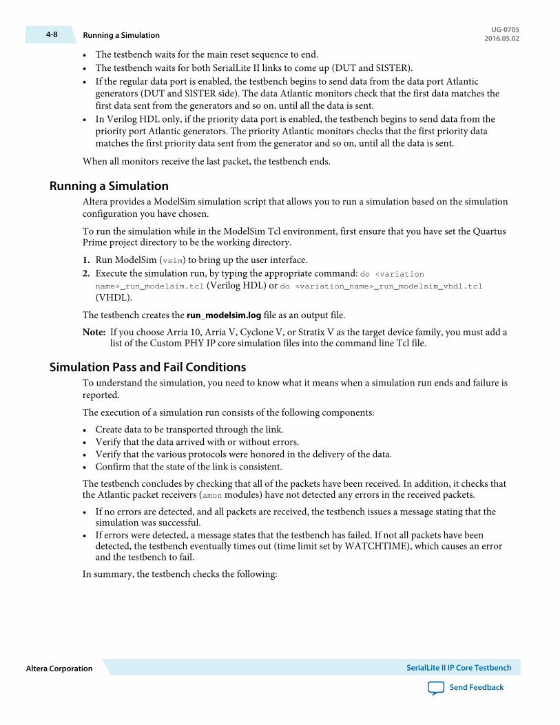
• The testbench waits for the main reset sequence to end.• The testbench waits for both SerialLite II links to come up (DUT and SISTER).• If the regular data port is enabled, the testbench begins to send data from the data port Atlantic
generators (DUT and SISTER side). The data Atlantic monitors check that the first data matches thefirst data sent from the generators and so on, until all the data is sent.
• In Verilog HDL only, if the priority data port is enabled, the testbench begins to send data from thepriority port Atlantic generators. The priority Atlantic monitors checks that the first priority datamatches the first priority data sent from the generator and so on, until all the data is sent.
When all monitors receive the last packet, the testbench ends.
Running a SimulationAltera provides a ModelSim simulation script that allows you to run a simulation based on the simulationconfiguration you have chosen.
To run the simulation while in the ModelSim Tcl environment, first ensure that you have set the QuartusPrime project directory to be the working directory.
1. Run ModelSim (vsim) to bring up the user interface.2. Execute the simulation run, by typing the appropriate command: do <variation
name>_run_modelsim.tcl (Verilog HDL) or do <variation_name>_run_modelsim_vhdl.tcl(VHDL).
The testbench creates the run_modelsim.log file as an output file.
Note: If you choose Arria 10, Arria V, Cyclone V, or Stratix V as the target device family, you must add alist of the Custom PHY IP core simulation files into the command line Tcl file.
Simulation Pass and Fail ConditionsTo understand the simulation, you need to know what it means when a simulation run ends and failure isreported.
The execution of a simulation run consists of the following components:
• Create data to be transported through the link.• Verify that the data arrived with or without errors.• Verify that the various protocols were honored in the delivery of the data.• Confirm that the state of the link is consistent.
The testbench concludes by checking that all of the packets have been received. In addition, it checks thatthe Atlantic packet receivers (amon modules) have not detected any errors in the received packets.
• If no errors are detected, and all packets are received, the testbench issues a message stating that thesimulation was successful.
• If errors were detected, a message states that the testbench has failed. If not all packets have beendetected, the testbench eventually times out (time limit set by WATCHTIME), which causes an errorand the testbench to fail.
In summary, the testbench checks the following:
4-8 Running a SimulationUG-0705
2016.05.02
Altera Corporation SerialLite II IP Core Testbench
Send Feedback

• Were all expected stimulus generated?• Did all expected packets arrive and was the data error-free?• If errors occurred on the data, did the SerialLite II logic detect the errors?• Were there any protocol errors?• Is there any evidence of the simulation running too long out of control?
If any of those checks detect a problem, the simulation is reported as failing. In a correctly operatingtestbench, the only reason for failing is the detection of deliberately inserted errors. There is a distinctionbetween a simulation run failing and a test failing. If you insert errors and the errors are detected, thesimulation fails. However, the test was successful because the errors were detected. For this reason,simulation failure is not by itself an indication of a problem. Example 5–1 shows the ModelSim log for asuccessful run.
Value Change Dump (VCD) File Generation (For the Verilog HDL Testbench)
The simulation allows .vcd file generation if WAVEFORM is tick defined. All signals are included in thedump file (dumpfile.vcd)
Testbench Time-OutThe testbench uses a maximum simulation time to guard against infinite loops or stuck simulations.
The default value of 500,000,000 picoseconds is sufficient for most simulation runs. If more time isneeded for a particularly long run, you can increase the WATCHTIME value.
• For Verilog HDL: Change the already defined WATCHTIME inside the testbench mainsection`define WATCHTIME 100,000,000.
• For VHDL: edit the <variation_name>_tb.vhd to change the constant WATCHTIME: time: =100000000 ns.
In Verilog HDL, instead of increasing gthe WATCHTIM, you could reset the watch timer from time totime (for example, after each test case or even after each packet is sent) by adding the following line, asneeded, to the testbench main section:
reset_watchdog_timer;
Every time the reset_watchdog_timer task is called, the testbench time-out resets with anotherWATCHTIME time.
Special Simulation Configuration Settings
The SerialLite II IP core contains few settings that have a reduced value in simulation:
• The internal counter that controls the duration of the digital resets to the ALTGX IP core counts up to20 in simulation.
• This count overrides the default value of 20,000. The clock compensation value determines when theclock compensation sequence is inserted into the high-speed serial stream (if Clock Compensation isenabled). In simulation, to minimize the time it takes for the sequence to occur, the value is always 100cycles, independent of the actual clock compensation time value —100 or 300 parts per million (ppm).
Atlantic Receiver Behavior
The receiver (Rx) Atlantic interface signals, other than rxhpp/rxrdp_val, can be x when the rxhpp/rxrdp_val is zero. Therefore, if the user logic uses the receive Atlantic interface when rxhpp/rxrdp_valis zero, the receiver IP core can transmit x’s when the data is not valid.
UG-07052016.05.02 Value Change Dump (VCD) File Generation (For the Verilog HDL Testbench) 4-9
SerialLite II IP Core Testbench Altera Corporation
Send Feedback

This invalid data should not be used during simulation. To ensure valid data transmission, the receiveAtlantic interface should only be sampled when the rxhpp/rxrdp_val is 1.
Testbench ComponentsThe components of the SerialLite testbench each has it own functions.
Table 4-1: Testbench Components Description
DUT The Verilog HDL or VHDL IP functional simulation model of thedevice under test (DUT)
SISTER A Verilog HDL or VHDL IP functional simulation model used to testthe DUT.
When the DUT is asymmetric (for example, the number of receivinglanes is different than the number of transmitting lanes), is configuredin single mode (receiver or transmitter only), or is configured inbroadcast mode, the SISTER parameters may not match the DUTparameters, or multiple SISTER MegaCore functions may need to beinstantiated.
AGEN This testbench includes separate versions of the AGEN module forVerilog HDL and VHDL.
AMON This testbench includes separate versions of the AMON module forVerilog HDL and VHDL.
Status Monitors (pin_mon) The simulation includes status pin monitors for the DUT and SISTERs(pin_mon_<pin_name>).
When enabled (by default), the status monitor compares the receiveddata against the expected data. If the expected value is different fromthe current value, the monitor flags an error.
Set the en input pin high to enable a pin monitor, low to disable a pinmonitor, or for Verilog HDL only use the tasks. The Verilog HDL pinmonitor expected value can be set by a task.
Clock and Reset Generator The DUT and the SISTER use a common clock, with the frequency setby the MegaWizard Plug-In Manager.
There is one master reset signal (reset_n) that resets all the logic in thedemonstration testbench (DUT, SISTER(s), AGENs, AMONs andstatus monitors).
Custom PHY IP Core The DUT and the SISTER use an external transceiver for Arria V andStratix V configurations. You are required to separately instantiate theCustom PHY IP core using the MegaWizard Plug-In Manager.
4-10 Testbench ComponentsUG-0705
2016.05.02
Altera Corporation SerialLite II IP Core Testbench
Send Feedback

AGENThis testbench includes separate versions of the AGEN module for Verilog HDL and VHDL.
Verilog HDL
• This Verilog HDL version of the AGEN module generates Atlantic data for the SerialLite IIdemonstration testbench (agen_dat_dut, agen_pri_dut, agen_dat_sis, agen_pri_sis, and so on). Thedata pattern is based on an LFSR to create a predictable but non-incrementing (pseudo-random)pattern. This module features few tasks, the main one being the send_packet task that transmitspackets into the SerialLite II MegaCore function. It also supports the streaming mode if the data port isconfigured as such.
• The first byte of each generated packet is a sequential identifier (id) that seeds the LFSR. Every time thesend_packet task is called, the agen id is incremented by one. The module operates in one of twomodes: data port or priority port. When in priority port mode, the Atlantic dav signal is ignored for allbut the first transfer of a packet. There can be multiple agen instantiations (for data and priority port,DUT and SISTER), depending on the DUT’s chosen parameters.
Table 4-2: AGEN Tasks
AGEN Tasks Description
send_packet(addr,size[31:0],err) send_packet is the main AGEN task. It causes a packet of aspecified size and destined for a particular address to betransmitted. The err bit may also be assigned a value. The datais based on a LFSR.
ipg(min[31:0],max[31:0]) If the gap task is called, successive packets are separated by arandom number of idle cycles.
gap(prob[31:0],min[31:0],max[31:0
])
If the iptg task is called, idle cycles are inserted between writeoperations. The probability of idles between write cyclesdecreases with larger values of prob.
verbose(bit_value) This task enables or disables the display of AGEN verbosemessages.
corrupt_sop This task corrupts the start of packet (SOP) of the next packet.When called, it waits for the SOP and corrupts it (makesSOP==0). All the subsequent packets are not corrupted.
corrupt_eop This task corrupts the end of packet (EOP) of the next packet.When called, it waits for the EOP and corrupts it (makesEOP==0). All the subsequent packets are not corrupted.
Table 4-3: send_packet Task Field Description
The table below describes the send_packet task fields.Field Location in
TaskField Valid Values Description
1 addr • 0 to 0xFF (data)• 0 to 0xF (priority)
Set to 0.
UG-07052016.05.02 AGEN 4-11
SerialLite II IP Core Testbench Altera Corporation
Send Feedback
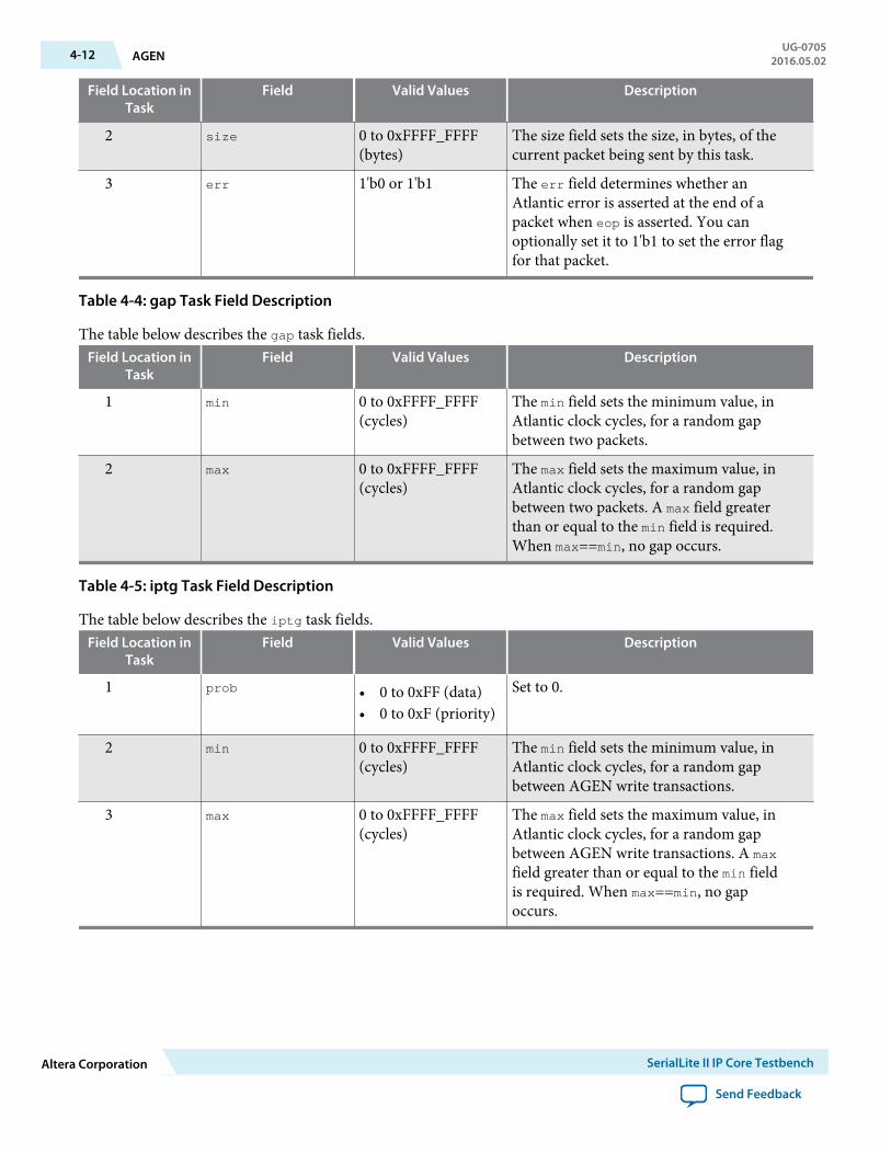
Field Location inTask
Field Valid Values Description
2 size 0 to 0xFFFF_FFFF(bytes)
The size field sets the size, in bytes, of thecurrent packet being sent by this task.
3 err 1'b0 or 1'b1 The err field determines whether anAtlantic error is asserted at the end of apacket when eop is asserted. You canoptionally set it to 1'b1 to set the error flagfor that packet.
Table 4-4: gap Task Field Description
The table below describes the gap task fields.Field Location in
TaskField Valid Values Description
1 min 0 to 0xFFFF_FFFF(cycles)
The min field sets the minimum value, inAtlantic clock cycles, for a random gapbetween two packets.
2 max 0 to 0xFFFF_FFFF(cycles)
The max field sets the maximum value, inAtlantic clock cycles, for a random gapbetween two packets. A max field greaterthan or equal to the min field is required.When max==min, no gap occurs.
Table 4-5: iptg Task Field Description
The table below describes the iptg task fields.Field Location in
TaskField Valid Values Description
1 prob • 0 to 0xFF (data)• 0 to 0xF (priority)
Set to 0.
2 min 0 to 0xFFFF_FFFF(cycles)
The min field sets the minimum value, inAtlantic clock cycles, for a random gapbetween AGEN write transactions.
3 max 0 to 0xFFFF_FFFF(cycles)
The max field sets the maximum value, inAtlantic clock cycles, for a random gapbetween AGEN write transactions. A maxfield greater than or equal to the min fieldis required. When max==min, no gapoccurs.
4-12 AGENUG-0705
2016.05.02
Altera Corporation SerialLite II IP Core Testbench
Send Feedback
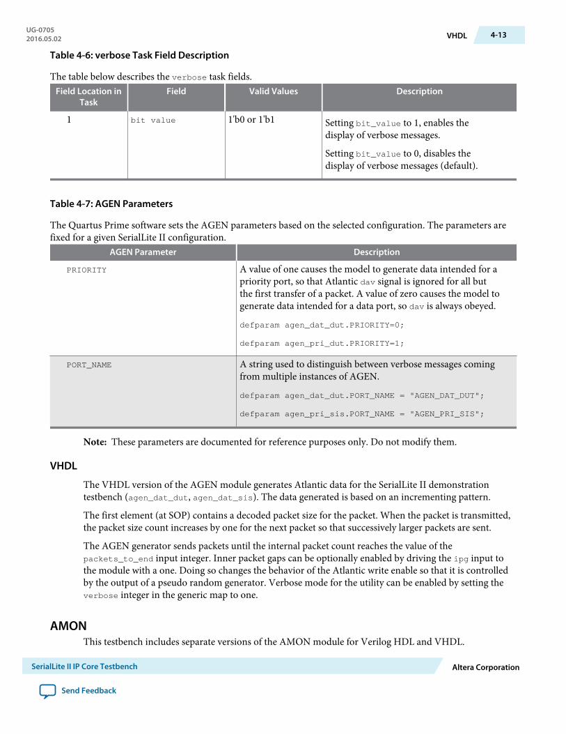
Table 4-6: verbose Task Field Description
The table below describes the verbose task fields.Field Location in
TaskField Valid Values Description
1 bit value 1'b0 or 1'b1 Setting bit_value to 1, enables thedisplay of verbose messages.
Setting bit_value to 0, disables thedisplay of verbose messages (default).
Table 4-7: AGEN Parameters
The Quartus Prime software sets the AGEN parameters based on the selected configuration. The parameters arefixed for a given SerialLite II configuration.
AGEN Parameter Description
PRIORITY A value of one causes the model to generate data intended for apriority port, so that Atlantic dav signal is ignored for all butthe first transfer of a packet. A value of zero causes the model togenerate data intended for a data port, so dav is always obeyed.
defparam agen_dat_dut.PRIORITY=0;
defparam agen_pri_dut.PRIORITY=1;
PORT_NAME A string used to distinguish between verbose messages comingfrom multiple instances of AGEN.
defparam agen_dat_dut.PORT_NAME = "AGEN_DAT_DUT";
defparam agen_pri_sis.PORT_NAME = "AGEN_PRI_SIS";
Note: These parameters are documented for reference purposes only. Do not modify them.
VHDL
The VHDL version of the AGEN module generates Atlantic data for the SerialLite II demonstrationtestbench (agen_dat_dut, agen_dat_sis). The data generated is based on an incrementing pattern.
The first element (at SOP) contains a decoded packet size for the packet. When the packet is transmitted,the packet size count increases by one for the next packet so that successively larger packets are sent.
The AGEN generator sends packets until the internal packet count reaches the value of thepackets_to_end input integer. Inner packet gaps can be optionally enabled by driving the ipg input tothe module with a one. Doing so changes the behavior of the Atlantic write enable so that it is controlledby the output of a pseudo random generator. Verbose mode for the utility can be enabled by setting theverbose integer in the generic map to one.
AMONThis testbench includes separate versions of the AMON module for Verilog HDL and VHDL.
UG-07052016.05.02 VHDL 4-13
SerialLite II IP Core Testbench Altera Corporation
Send Feedback

The Verilog HDL version of the AMON module monitors the Atlantic data received (instances:amon_dat_dut, amon_pri_dut, amon_dat_sis, amon_pri_sis, and so on). The data pattern receivedmust be based on a LFSR that has produced a predictable but non-incrementing pattern.
The AMON monitor does the following basic checks:
• Data checking: checks that the received data follows the LFSR pattern.• id checking: checks that the packet identifier (first byte of each packet) is an incrementing number.• Number of packets checking: checks that the expected number of regular data or high priority packets
have been received. The expected number of packets is set via tasks.• Start or end of packet checking: checks Atlantic packets for missing SOP and EOP signals.
The module operates in one of two modes: data port or priority port. When in priority port mode, the davsignal is ignored for all but the first transfer of a packet.
There can be multiple AMON instantiations (for data and priority port, DUT and SISTER), depending onthe DUT’s chosen parameters.
Table 4-8: AMON Tasks
AGEN Tasks Description
data_checking(bit_value)) This task enables or disables the data checking.
id_checking(bit_value) This task enables or disables the packet id checking.
wait_all_packets(number[31:0]) This task waits until all packets (when in packet mode) orstreaming bytes (when in streaming mode) are received.
mp_checking(bit_value) This task enables or disables the missing SOP and EOPchecking.
gap(prob[31:0],min[31:0],max[31:0
])p
If this task is called, amon read operations may have some gapsbetween them. The probability of gaps between read cyclesdecreases with larger values of prob.
verbose (bit_value) This task enables or disables the display of verbose messages.
Table 4-9: data_checking Task Field Description
The table below describes the data_checking task fields.Field Location in
TaskField Valid Values Description
1 bit_value 1'b0 or 1'b1 Setting bit_value to 1, enables the datachecking (default).
Setting bit_value to 0, disables the datachecking.
4-14 AMONUG-0705
2016.05.02
Altera Corporation SerialLite II IP Core Testbench
Send Feedback
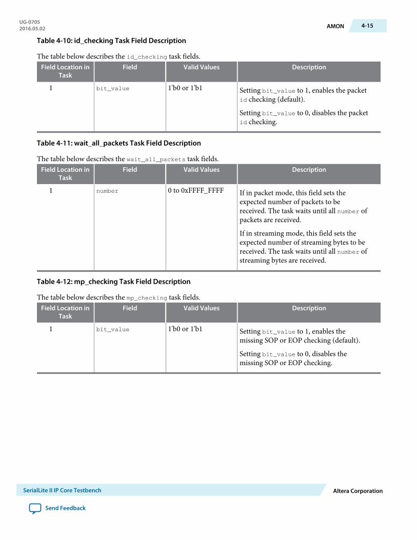
Table 4-10: id_checking Task Field Description
The table below describes the id_checking task fields.Field Location in
TaskField Valid Values Description
1 bit_value 1'b0 or 1'b1 Setting bit_value to 1, enables the packetid checking (default).
Setting bit_value to 0, disables the packetid checking.
Table 4-11: wait_all_packets Task Field Description
The table below describes the wait_all_packets task fields.Field Location in
TaskField Valid Values Description
1 number 0 to 0xFFFF_FFFF If in packet mode, this field sets theexpected number of packets to bereceived. The task waits until all number ofpackets are received.
If in streaming mode, this field sets theexpected number of streaming bytes to bereceived. The task waits until all number ofstreaming bytes are received.
Table 4-12: mp_checking Task Field Description
The table below describes the mp_checking task fields.Field Location in
TaskField Valid Values Description
1 bit_value 1'b0 or 1'b1 Setting bit_value to 1, enables themissing SOP or EOP checking (default).
Setting bit_value to 0, disables themissing SOP or EOP checking.
UG-07052016.05.02 AMON 4-15
SerialLite II IP Core Testbench Altera Corporation
Send Feedback

Table 4-13: read_transaction_gap Task Field Description
The table below describes the read_transaction_gap task fields.Field Location in
TaskField Valid Values Description
1 prob 0 to 0xFFFF_FFFF(integer)
The prob field sets the probability for aread transaction gap to happen.Probability decreases with a larger value ofprob.
Before each read transaction a randomnumber between 0 and prob is generatedand compared to prob/2. If they match, arandom gap is inserted in the readoperation (ena goes low); if not, no gap isinserted.
2 min 0 to 0xFFFF_FFFF(cycles)
The min field sets the minimum value, inAtlantic clock cycles, for a random gapbetween AMON read transactions.
3 max 0 to 0xFFFF_FFFF(cycles)
The max field sets the maximum value, inAtlantic clock cycles, for a random gapbetween AMON read transactions.
A max field greater than or equal to themin field is required. When max==min, nogap occurs.
Table 4-14: verbose Task Field Description
The table below describes the verbose task fields.Field Location in
TaskField Valid Values Description
1 bit value 1'b0 or 1'b1 Setting bit_value to 1, enables thedisplay of verbose messages.
Setting bit_value to 0, disables thedisplay of verbose messages (default).
4-16 AMONUG-0705
2016.05.02
Altera Corporation SerialLite II IP Core Testbench
Send Feedback

Table 4-15: AMON Parameters
The Quartus Prime software sets the AMON parameters based on the selected configuration. The parameters arefixed for a given SerialLite II configuration.
AMON Parameter Description
PRIORITY A value of one causes the model to generate data intended for apriority port, so that Atlantic dav signal is ignored for all butthe first transfer of a packet. A value of zero causes the model togenerate data intended for a data port, so dav is always obeyed.
defparam amon_dat_dut.PRIORITY=0;
defparam amon_pri_dut.PRIORITY=1;
PORT_NAME A string used to distinguish between verbose messages comingfrom multiple instances of AGEN.
defparam amon_dat_dut.PORT_NAME = "AMON_DAT_DUT";
defparam amon_pri_sis.PORT_NAME = "AMON_PRI_SIS";
Note: These parameters are documented for reference purposes only. Do not modify them.
VHDL
The VHDL version of the AMON module monitors the Atlantic data received (instances:amon_dat_dut,amon_dat_sis). The data received is based on a incrementing pattern.
The AMON monitor performs the following functions:
• Validates transmission of individual packets by extracting the intended packet size from the SOP andchecking it against the actual value of the packet size counter in the EOP.
• Counts the total number of packets (provided as an output) to ensure that the all packets sent are alsoreceived.
• Checks Atlantic packets for missing SOP and EOP signals.
If any errors are detected by the AMON monitor, the error_detect output signal is asserted.
Inner packet read gaps can optionally be enabled by driving the ipg input to the module with a one.Doing so changes the behavior of the Atlantic read enable so that it is instead controlled by the output of apseudo random generator. Verbose mode for the utility is enabled by setting the verbose integer in thegeneric map to one.
Status MonitorsThe simulation includes status pin monitors (pin_mon) for the DUT and SISTERs(pin_mon_<pin_name>). When enabled (by default), the status monitor compares the received dataagainst the expected data. If the expected value is different from the current value, the monitor flags anerror.
Set the en input pin high to enable a pin monitor, low to disable a pin monitor, or for Verilog HDL onlyuse the tasks. The Verilog HDL pin monitor expected value can be set by a task.
UG-07052016.05.02 VHDL 4-17
SerialLite II IP Core Testbench Altera Corporation
Send Feedback

Table 4-16: Pin Monitor Tasks (Verilog HDL)
pin_mon Tasks Description
on This task enables monitoring (the en input pin must also be sethigh to enable monitoring).
off This task disables monitoring (regardless of the value of the eninput pin).
verbose_on This task enables the display of verbose messages.
verbose_off This task disables the display of verbose messages.
set_expect (bit value) This task sets the expected pin value.
Clock and Reset GeneratorThe DUT and the SISTER use a common clock, with the frequency set by the Quartus Prime software.
There is one master reset signal (reset_n) that resets all the logic in the demonstration testbench (DUT,SISTER(s), AGENs, AMONs, and status monitors).
Note: Ensure reset_n to the IP core starts high at Time=0, and then goes low for proper reset of thesimulation model. Some simulators do not detect the transition if reset_n is asserted low atTime=0.
To allow for easy modification, the reset section of the testbench is marked by start–end comment tags:
SERIALLITE2_TB_RESET_START
ERIALLITE2_TB_RESET_END
The clock and reset utilities are included in the testbench top-level file.
Custom PHY IP CoreThe DUT and the SISTER use an external transceiver for Arria 10, Arria V, Cyclone V, and Stratix Vconfigurations.
You are required to separately instantiate the Custom PHY IP core using the Quartus Prime software.
Example Testbench – Verilog HDLBecause there is no Atlantic to Atlantic score-boarding, the demonstration testbench focuses on passingerror-free data rather than errored data. Any error condition that involves dropped or errored packets,must be handled in the testbench by setting proper expectations
To allow for easy modification of the demonstration testbench, its main section is marked by start–endtags:
//SERIALLITE2_TB_MAIN_START
//SERIALLITE2_TB_MAIN_END
Note: This example testbench may not match your testbench exactly.
4-18 Clock and Reset GeneratorUG-0705
2016.05.02
Altera Corporation SerialLite II IP Core Testbench
Send Feedback

Table 4-17: Example of a Demonstration Testbench
The table shows and explains a demonstration testbench main section example, allowing you to easily modify thetestbench. You can change the packet size, port address, number of packets, and so on, or force certain behavior.
Main Section Comments
//SERIALLITE2_TB_MAIN_START Start of the testbench main section; the only section intended to bemodified.
integer pkt_cnt_dat_dut;
integer pkt_cnt_pri_dut;
integer pkt_cnt_dat_sis;
integer pkt_cnt_pri_sis;
Declare packet counters.
//--------------------------
----------------------------
--- //Define the number of
packets / streaming bytes to
be sent //------------------
----------------------------
----------- integer packets_
to_send; initial packets_to_
send = 5; integer streaming_
bytes; initial streaming_
bytes = 1500; //------------
----------------------------
-----------------
Defines the number of packets (5) or streaming bytes (1,500) to besent.
initial begin #1; Main initial block.
exp_tc_cnt = 1; Sets expectation for the number of test cases (checks); this numbermust match the number of tc_start/tc_end pairs in the testbench,otherwise the testbench is declared INCOMPLETE.
err_limit = 0; Sets expectation for the number of errors.
tc_start(`TBID); Testcase start.
wait (reset_n == 1); Waiting for the reset to complete; the reset is asserted in a separateinitial block.
// initialize packet
counters
pkt_cnt_dat_dut = packets_
to_send;
Sets the number of packets to be sent to the regular data port of theDUT IP core.
pkt_cnt_pri_dut = packets_
to_send;
Sets the number of packets to be sent to the high priority port of theDUT IP core.
UG-07052016.05.02 Example Testbench – Verilog HDL 4-19
SerialLite II IP Core Testbench Altera Corporation
Send Feedback
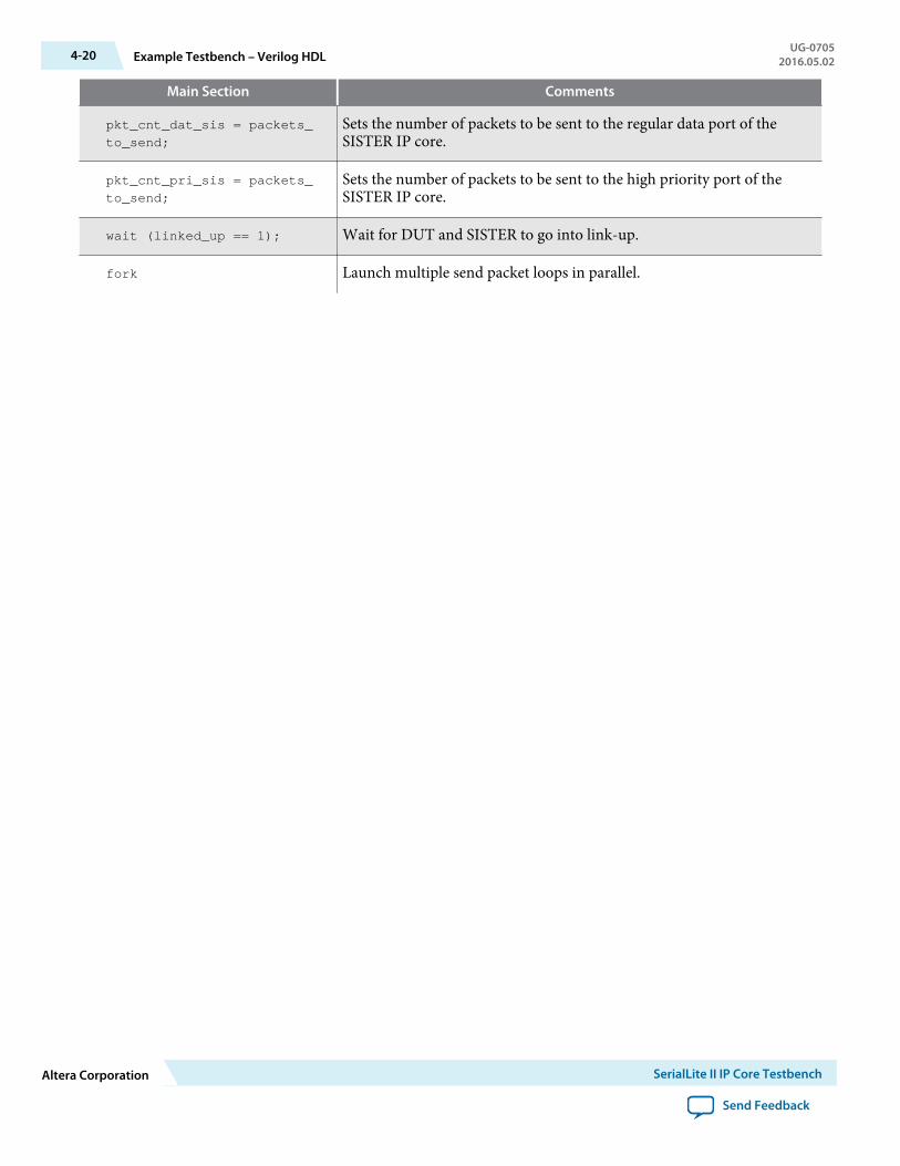
Main Section Comments
pkt_cnt_dat_sis = packets_
to_send;
Sets the number of packets to be sent to the regular data port of theSISTER IP core.
pkt_cnt_pri_sis = packets_
to_send;
Sets the number of packets to be sent to the high priority port of theSISTER IP core.
wait (linked_up == 1); Wait for DUT and SISTER to go into link-up.
fork Launch multiple send packet loops in parallel.
4-20 Example Testbench – Verilog HDLUG-0705
2016.05.02
Altera Corporation SerialLite II IP Core Testbench
Send Feedback
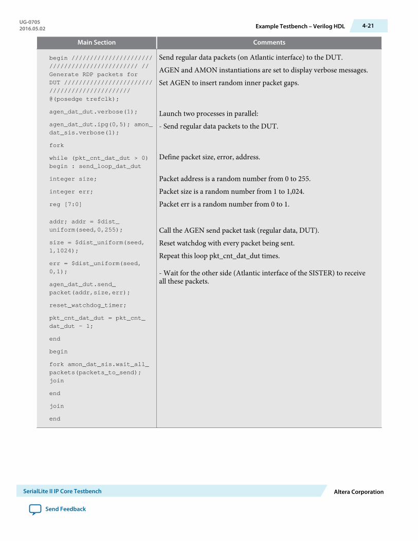
Main Section Comments
begin //////////////////////
//////////////////////// //
Generate RDP packets for
DUT ////////////////////////
//////////////////////
@(posedge trefclk);
agen_dat_dut.verbose(1);
agen_dat_dut.ipg(0,5); amon_
dat_sis.verbose(1);
fork
while (pkt_cnt_dat_dut > 0)
begin : send_loop_dat_dut
integer size;
integer err;
reg [7:0]
addr; addr = $dist_
uniform(seed,0,255);
size = $dist_uniform(seed,
1,1024);
err = $dist_uniform(seed,
0,1);
agen_dat_dut.send_
packet(addr,size,err);
reset_watchdog_timer;
pkt_cnt_dat_dut = pkt_cnt_
dat_dut - 1;
end
begin
fork amon_dat_sis.wait_all_
packets(packets_to_send);
join
end
join
end
Send regular data packets (on Atlantic interface) to the DUT.
AGEN and AMON instantiations are set to display verbose messages.
Set AGEN to insert random inner packet gaps.
Launch two processes in parallel:
- Send regular data packets to the DUT.
Define packet size, error, address.
Packet address is a random number from 0 to 255.
Packet size is a random number from 1 to 1,024.
Packet err is a random number from 0 to 1.
Call the AGEN send packet task (regular data, DUT).
Reset watchdog with every packet being sent.
Repeat this loop pkt_cnt_dat_dut times.
- Wait for the other side (Atlantic interface of the SISTER) to receiveall these packets.
UG-07052016.05.02 Example Testbench – Verilog HDL 4-21
SerialLite II IP Core Testbench Altera Corporation
Send Feedback
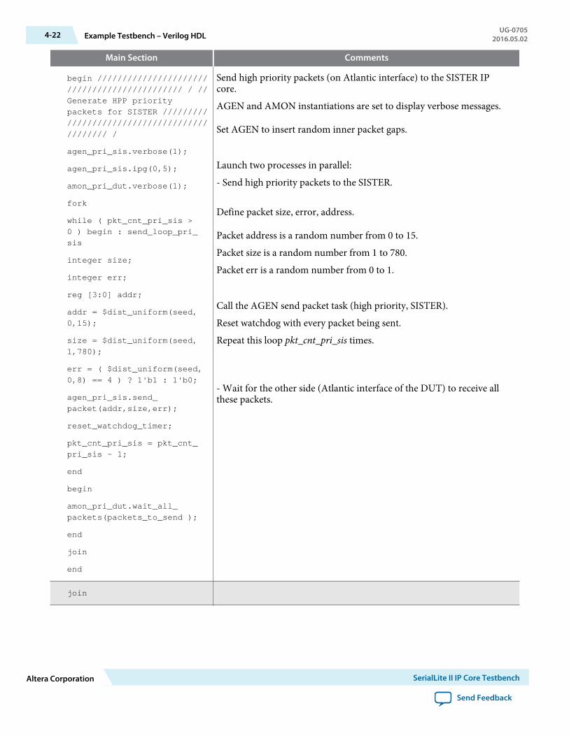
Main Section Comments
begin //////////////////////
/////////////////////// / //
Generate HPP priority
packets for SISTER /////////
////////////////////////////
//////// /
agen_pri_sis.verbose(1);
agen_pri_sis.ipg(0,5);
amon_pri_dut.verbose(1);
fork
while ( pkt_cnt_pri_sis >
0 ) begin : send_loop_pri_
sis
integer size;
integer err;
reg [3:0] addr;
addr = $dist_uniform(seed,
0,15);
size = $dist_uniform(seed,
1,780);
err = ( $dist_uniform(seed,
0,8) == 4 ) ? 1'b1 : 1'b0;
agen_pri_sis.send_
packet(addr,size,err);
reset_watchdog_timer;
pkt_cnt_pri_sis = pkt_cnt_
pri_sis - 1;
end
begin
amon_pri_dut.wait_all_
packets(packets_to_send );
end
join
end
Send high priority packets (on Atlantic interface) to the SISTER IPcore.
AGEN and AMON instantiations are set to display verbose messages.
Set AGEN to insert random inner packet gaps.
Launch two processes in parallel:
- Send high priority packets to the SISTER.
Define packet size, error, address.
Packet address is a random number from 0 to 15.
Packet size is a random number from 1 to 780.
Packet err is a random number from 0 to 1.
Call the AGEN send packet task (high priority, SISTER).
Reset watchdog with every packet being sent.
Repeat this loop pkt_cnt_pri_sis times.
- Wait for the other side (Atlantic interface of the DUT) to receive allthese packets.
join
4-22 Example Testbench – Verilog HDLUG-0705
2016.05.02
Altera Corporation SerialLite II IP Core Testbench
Send Feedback
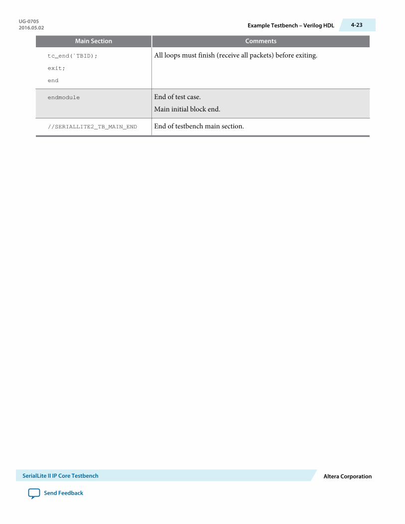
Main Section Comments
tc_end(`TBID);
exit;
end
All loops must finish (receive all packets) before exiting.
endmodule End of test case.
Main initial block end.
//SERIALLITE2_TB_MAIN_END End of testbench main section.
UG-07052016.05.02 Example Testbench – Verilog HDL 4-23
SerialLite II IP Core Testbench Altera Corporation
Send Feedback
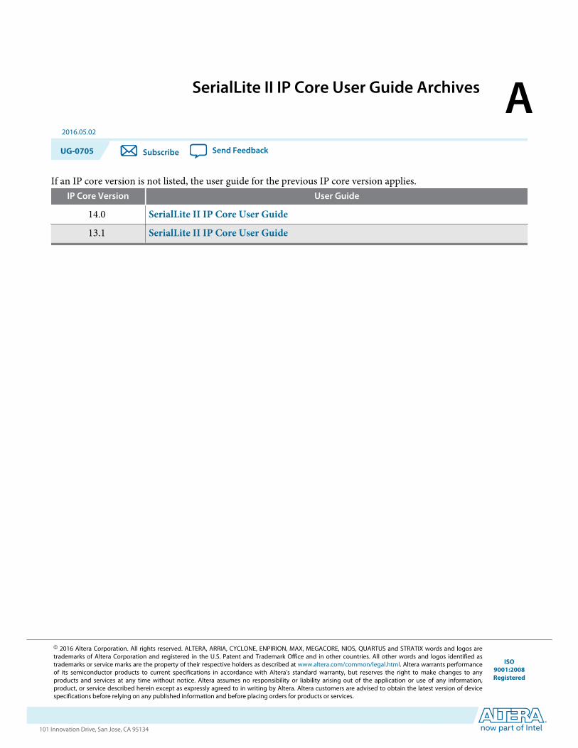
SerialLite II IP Core User Guide Archives A2016.05.02
UG-0705 Subscribe Send Feedback
If an IP core version is not listed, the user guide for the previous IP core version applies.IP Core Version User Guide
14.0 SerialLite II IP Core User Guide
13.1 SerialLite II IP Core User Guide
© 2016 Altera Corporation. All rights reserved. ALTERA, ARRIA, CYCLONE, ENPIRION, MAX, MEGACORE, NIOS, QUARTUS and STRATIX words and logos aretrademarks of Altera Corporation and registered in the U.S. Patent and Trademark Office and in other countries. All other words and logos identified astrademarks or service marks are the property of their respective holders as described at www.altera.com/common/legal.html. Altera warrants performanceof its semiconductor products to current specifications in accordance with Altera's standard warranty, but reserves the right to make changes to anyproducts and services at any time without notice. Altera assumes no responsibility or liability arising out of the application or use of any information,product, or service described herein except as expressly agreed to in writing by Altera. Altera customers are advised to obtain the latest version of devicespecifications before relying on any published information and before placing orders for products or services.
ISO9001:2008Registered
www.altera.com101 Innovation Drive, San Jose, CA 95134

Revision History for SerialLite II IP Core UserGuide B
2016.05.02
UG-0705 Subscribe Send Feedback
Date Version Changes
May 2016 2016.05.02 • Edited aggregate bandwidth information—the input data bus intothe processor portion is 36 bits wide (32 bits of raw data and 8 bitsof control information).
• Added indirect support for Arria 10 devices. Contact an Alterarepresentative or file a Service Request (SR) to use the Arria 10devices.
• Updated transceiver information for Arria 10, Arria V, Cyclone V,and Stratix V devices. You need to generate the Custom PHY IPcore for these devices.
• Changed instances of Quartus II to Quartus Prime.• Added links to archived versions of the SerialLite II IP Core User
Guide.
July 2014 2014.07.09 • Replaced MegaWizard Plug-In Manager information with IPCatalog.
• Added standard information about upgrading IP cores.• Added standard installation and licensing information.• Removed obsolete device information.
January 2014 13.1 • Removed information about Arria GX, HardCopy IV, Stratix GX,and Stratix II GX devices. Altera no longer supports these devices.
• Added Cyclone V device support.• Updated data rate information.
July 2012 12.0 • Added Arria V and Stratix V device support.• Added information about MegaCore configuration for Arria V and
Stratix V devices.
February 2011 10.1 • Updated Arria II GX and Stratix IV device support information.• Added information about FIFO threshold settings.
© 2016 Altera Corporation. All rights reserved. ALTERA, ARRIA, CYCLONE, ENPIRION, MAX, MEGACORE, NIOS, QUARTUS and STRATIX words and logos aretrademarks of Altera Corporation and registered in the U.S. Patent and Trademark Office and in other countries. All other words and logos identified astrademarks or service marks are the property of their respective holders as described at www.altera.com/common/legal.html. Altera warrants performanceof its semiconductor products to current specifications in accordance with Altera's standard warranty, but reserves the right to make changes to anyproducts and services at any time without notice. Altera assumes no responsibility or liability arising out of the application or use of any information,product, or service described herein except as expressly agreed to in writing by Altera. Altera customers are advised to obtain the latest version of devicespecifications before relying on any published information and before placing orders for products or services.
ISO9001:2008Registered
www.altera.com101 Innovation Drive, San Jose, CA 95134

Date Version Changes
July 2010 10.0 Updated Stratix IV device support information.
November 2009 9.1 • Added HardCopy IV GX device support.• Added timing diagrams in Initialization and Restart, and Atlantic
Interface sections.
March 2009 9.0 Added Arria II GX device support.
November 2008 8.1 Added requirement to configure a dynamic reconfiguration block withStratix IV transceivers, to enable offset equalization.
May 2008 8.0 • Added additional ALT2GXB parameters - VCCH, Reference InputClk Frequency, and Reconfiguration Channel Number.
• Added Stratix IV device support.
October 2007 7.2
(Beta)
• Added gxb_powerdown signal to ease merging of multiple SerialLiteII cores into the same transceiver block.
• Added VHDL testbench for some configurations.• Moved the ALT2GXB megafunction instantiation into a separate
file to ease post-generation changes.
B-2 Revision History for SerialLite II IP Core User GuideUG-0705
2016.05.02
Altera Corporation Revision History for SerialLite II IP Core User Guide
Send Feedback


