Subcommittee Chair: Leland Chang, IBM, Yorktown Heights, NY
SRAM continues to be the critical technology enabler for a wide range of applications from low-power to high-performance computing.This session showcases the leading-edge SRAM developments from the semiconductor industry. Intel presents the smallest SRAMbitcell for 10nm technology, with design assist techniques to enable low VMIN operation. Samsung presents the smallest bitcell for7nm technology and shows a double-write driver technique to further improve VMIN. TSMC demonstrates a 7nm 5GHz L1 cache forhigh-performance computing.
Session Chair: Jonathan Chang
TSMC, Hsinchu, Taiwan
Associate Chair: Chun Shiah
Etron, Hsinchu, Taiwan
195DIGEST OF TECHNICAL PAPERS •
ISSCC 2018 / February 13, 2018 / 8:30 AM
8:30 AM11.1 A 23.6Mb/mm2 SRAM in 10nm FinFET Technology with Pulsed PMOS TVC and Stepped-WL for Low-
Voltage ApplicationsZ. Guo, Intel, Hillsboro, ORIn Paper 11.1, Intel presents a 23.6Mb/mm2 SRAM in 10nm FinFET with the smallest 10nm SRAM bitcell.It adopts column-based transient voltage collapse and a stepped wordline to lower the minimum operationvoltage (VMIN).
9:00 AM11.2 A 7nm FinFET SRAM Using EUV Lithography with Dual Write-Driver-Assist Circuitry for Low-Voltage
ApplicationsT. Song, Samsung Electronics, Hwaseong, KoreaIn Paper 11.2, Samsung Electronics presents a 7nm FinFET SRAM using EUV lithography. It adopts a0.026μm2 bitcell and VMIN is improved with a proposed dual write-driver (DWD) scheme in combinationwith a negative bitline scheme.
9:30 AM11.3 A 5GHz 7nm L1 Cache Memory Compiler for High-Speed Computing and Mobile Applications
M. Clinton, TSMC, Austin, TXIn Paper 11.3, TSMC presents a 7nm L1 cache memory compiler, which operates at a 5GHz clockfrequency. It implements a self-timing scheme with small-signal sensing and a folded architecture toincrease the performance.
11
196 • 2018 IEEE International Solid-State Circuits Conference
ISSCC 2018 / SESSION 11 / SRAM / 11.1
11.1 A 23.6Mb/mm2 SRAM in 10nm FinFET Technology with Pulsed PMOS TVC and Stepped-WL for Low-Voltage Applications
Zheng Guo, Daeyeon Kim, Satyanand Nalam, Jami Wiedemer,Xiaofei Wang, Eric Karl
Intel, Hillsboro, OR
The emergence of cloud computing and big data analytics, accompanied by asustained growth of battery-powered mobile devices, continues to drive theimportance of energy and area efficient CPU and SoC designs. Low-voltageoperation remains one of the primary approaches for active power reduction, butSRAM VMIN can limit the minimum operating voltage. Device size quantizationcontinues to be a challenge for compact 6T SRAM design in FinFET technologies,where careful co-optimization of the technology and assist circuit design isrequired for high-density low-voltage array implementations. This paper presentstwo SRAM array designs in a 10nm low-power CMOS technology featuring 3rd
generation FinFET transistors: a high-density 23.6Mb/mm2 array and a low-voltage20.4Mb/mm2 array.
Figure 11.1.1 shows the layout diagrams of a 0.0312μm2 high-density 6T SRAMcell (HDC) and a 0.0367μm2 low-voltage 6T SRAM cell (LVC) in a 10nm FinFETtechnology. The HDC utilizes minimum sized devices, with a fin ratio of 1:1:1(PU:PG:PD), to minimize cell area, while the LVC features a larger PD device(1:1:2) for improved read stability at low voltage. Self-aligned quad patterning(SAQP) is introduced on critical layers to achieve fin pitches down to 34nm andmetal pitches down to 36nm with 193nm immersion lithography [1], enabling a0.62x area scaling of the 6T SRAM cell relative to a 14nm technology [2]. Tofurther maximize density scaling of the 10nm technology, several key architecturalfeatures have been added to achieve further array area scaling of the 128kb HDCand LVC macros: achieving a 0.58x and 0.57x reduction relative to 14nmequivalents. Figure 11.1.1 highlights the cell area (μm2) and array area (mm2/Mb)of recently reported 6T SRAM designs from 14nm, 10nm and 7nm technologies[2-4].
Figure 11.1.2 details two architectural features of the 10nm technology forimproved density [1]. The first eliminates the need for isolation dummy gates byintroducing a minimum isolation step at the source/drain boundary to isolateneighboring transistors by the width of a single gate. The second enables theplacement of gate contacts over active transistors, thus eliminating the need forgate extension over isolation to land contacts. The tables in Fig. 11.1.2 summarizethe area scaling of critical SRAM periphery circuits, and the array efficiency anddensity of 128kb SRAM macros in 14nm and 10nm technologies. Thecombination of single-gate isolation, enabling contacts over active gates, alongwith the improved pitch scaling of critical interconnect layers has enabledaggressive area scaling of critical SRAM peripheral logic from 14nm to 10nm withminimum fin depopulation. As a result, a 77.1% array efficiency and a23.6Mb/mm2 density are achieved for a 128kb HDC macro: a 5.4% area efficiencyimprovement over a comparable 14nm design. A 78.4% array efficiency and a20.4Mb/mm2 density are achieved for a 128kb LVC macro: a 6.8% area efficiencyimprovement over a comparable 14nm design.
Wordline underdrive (WLUD) is used to improve the low-voltage read and half-select stability of an SRAM cell: trading off performance for VMIN [2]. To minimizethe impact of interconnect resistance on WL voltage uniformity between differentrows of the decoder, WLUD PMOS devices are implemented locally in the WLdriver using a matched layout and routing across neighboring rows. To improvethe low-voltage write margin, a column-based transient voltage collapse (TVC)scheme is employed to weaken the PU transistor during a write [2]. In this work,a PMOS device (PWR) is used to discharge the memory cell supply (VCS).Compared to an NMOS device, a PMOS device improves VCS control, but at thecost of discharge speed. VCS can be regulated by PMOS bias devices (PB[1:0]),as is illustrated in Fig. 11.1.3. To minimize write energy overhead, a pulsed VCS
collapse can be applied with no bias current [2]. To avoid half-select instabilityalong the column, due to a low VCS, careful control of the TVC pulse must beimplemented across a range of array configurations when using pulsed TVC. Sincethe PMOS transistor drive strength degrades super-linearly with a falling VCS inthis configuration, wider TVC pulses can be applied without requiring a biascurrent to avoid half-select instability. VCS sensitivity to the TVC pulse-width and/or
array configuration is also reduced, and can be further adjusted by tuning thePMOS transistor Vt. If PMOS bias is required, VCS can be determined by the voltagedivision across PWR and PB[1:0]. The resulting voltage level correlates well tothe write margin, compared to an NMOS TVC that can produce a higher VCS underprocess skew with a lower NMOS:PMOS drive ratio, where the SRAM write marginis degraded.
While WLUD is effective for enhancing read stability, it degrades the write margin.To independently improve the 6T cell’s read and write VMIN, a stepped-wordline(S-WL) scheme [5,6] is implemented to complement the pulsed PMOS TVC writeassist. Figure 11.1.3 details the design of the S-WL and PMOS TVC in a 128kbSRAM macro. WLUD pulses (WLUDPULSE[2:0]) are generated from static WLUDbias controls (WLBIAS[2:0]) and the read/write clock. WL suppression is firstenabled to create a sufficient BL separation that reinforces cell stability, beforeWLUDPULSE[2:0] are adjusted to restore the WL to a higher voltage level. Sincethe required BL differential needed to improve read stability is higher than thevoltage sensing margin, the read performance is not impacted by S-WL operation.To maximize the effectiveness of the TVC write assist, the TVC pulse is delayedto align it with WL restoration. To minimize interconnect delay along the WLCLK#and WLUDPULSE paths, local buffers are implemented to drive across the 32bsections of the 256b decoder. This reduces the distributed WLCLK# andWLUDPULSE gate loading by 8×, while maintaining the same logic depth for WLgeneration. Control logic for S-WL is implemented in the timer/control region witha negligible area overhead.
Figure 11.1.4 shows the simulation waveforms during a write cycle using staticWLUD, no WLUD and S-WL. With static WLUD, WL is suppressed for the durationof the WL pulse to maintain cell stability while degrading the write margin. Turningoff WLUD improves write margin, but compromises read stability. When S-WL isenabled, the WL is suppressed during the first phase to maintain cell stability.After a sufficient BL separation is achieved, WLBIAS#[2:0] are adjusted to raisethe WL voltage, aligned to the TVC pulse, to improve the write margin.
Figure 11.1.5 shows the measured voltage-frequency shmoos of the HDC SRAMusing pulsed PMOS TVC write assist, complemented by static WLUD, no WLUDand S-WL. The WL voltage level during the first phase of S-WL matches the staticWLUD level. S-WL enables an 80mV and a 100mV improvement to VMIN,compared to a static WLUD and no WLUD. Compared to S-WL operation, arrayperformance is improved with no WLUD due to the higher WL voltage over theentire WL pulse, but VMIN increases due to degraded read stability. In contrast,array performance for static WLUD is limited by the suppressed WL writeoperation. Figure 11.1.6 summarizes the write and read VMIN measurements forHDC and LVC using a static WLUD and S-WL, with pulsed PMOS TVC. Similar tothe voltage-frequency measurements, the WL voltage level during the first phaseof S-WL matches the static WLUD level, as determined by the memory cell readstability requirement. S-WL operation enables a 150mV write VMIN improvementfor HDC at the 90th percentile and a 60mV write VMIN improvement for LVC at the90th percentile, without degrading the read VMIN. Decreased write VMIN improvementis observed for LVC due to the reduced WLUD applied. A die micrograph of the10nm test vehicle with 72Mb of LVC SRAM and 54Mb of HDC SRAM is shown inFig. 11.1.7.
References:[1] C. Auth, et al., “A 10nm High Performance and Low-Power CMOS TechnologyFeaturing 3rd Generation FinFET Transistors, Self-Aligned Quad Patterning,Contact over Active Gate and Cobalt Local Interconnects”, IEDM, 2017.[2] E. Karl, et al., "A 0.6V, 1.5GHz 84Mb SRAM Design in 14nm FinFET CMOSTechnology", ISSCC, pp. 310-311, 2015.[3] K.-I. Seo, et al., “A 10nm Platform Technology for Low Power and HighPerformance Application Featuring FINFET Devices with Multi Workfunction GateStack on Bulk and SOI”, Symp. VLSI Tech., pp. 12-13, 2014.[4] J. Chang, et al., “A 7nm 256Mb SRAM in High-K Metal-Gate FinFETTechnology with Write-Assist Circuitry for Low-VMIN Applications”, ISSCC, pp.206-207, 2017.[5] K. Takeda, et al., “Multi-step Word-line Control Technology in Hierarchical CellArchitecture for Scaled-down High-density SRAMs”, IEEE Symp. VLSI Circuits,pp. 101-102, 2010.[6] J. Chang, et al., “A 20nm 112Mb SRAM in High-κ Metal-Gate with AssistCircuitry for Low-Leakage and Low-VMIN Applications”, ISSCC, pp. 316-317, 2013.
Figure 11.1.1: (top) 10nm HDC and LVC 6T SRAM cells. (bottom) Bitcell andarray area scaling trends.
Figure 11.1.2: (top) 10nm technology features. (middle and bottom) Impact onarray efficiency and array density.
Figure Figure 11.1.3: PMOS TVC circuit, and WLUD circuit with S-WL feature.
Figure 11.1.5: Measured voltage-frequency shmoo for HDC with (top) PMOSTVC and static WLUD compared to TVC and S-WL, and (bottom) TVC and noWLUD compared to TVC and S-WL.
Figure 11.1.6: Measured write and read VMIN distribution for HDC and LVC withPMOS TVC plus static WLUD and S-WL.
Figure 11.1.4: Simulation waveforms with (left) PMOS TVC and static WLUD,(middle) TVC and no WLUD, and (right) TVC and S-WL.
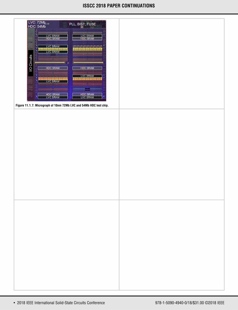
Figure 11.1.7: Micrograph of 10nm 72Mb LVC and 54Mb HDC test chip.
198 • 2018 IEEE International Solid-State Circuits Conference
ISSCC 2018 / SESSION 11 / SRAM / 11.2
11.2 A 7nm FinFET SRAM Using EUV Lithography with Dual Write-Driver-Assist Circuitry for Low-Voltage Applications
Taejoong Song, Jonghoon Jung, Woojin Rim, Hoonki Kim, Yongho Kim, Changnam Park, Jeongho Do, Sunghyun Park, Sungwee Cho, Hyuntaek Jung, Bongjae Kwon, Hyun-Su Choi, JaeSeung Choi, Jong Shik Yoon
Samsung Electronics, Hwaseong, Korea
SRAM plays an integral role in the power, performance, and area of a mobilesystem-on-a-chip. To achieve low power and high density, extreme ultraviolet(EUV) technology is adopted for the 7nm FinFET technology [3-4]. ConventionalArF immersion with a single exposure for an extreme high-resolution patterningshows the limitation of lithographic patterning. Therefore, multi-patterninglithographic technique is applied to support a high-resolution lithography.However, this also includes process variations due to using multi-pattering masks.Alternatively, EUV offers competitive scaling with a single-mask with the benefitof smaller wavelength, which provides smaller process variation with lessadditional pattering. Figure 11.2.1 shows a 7nm EUV FinFET 6T high-density (HD)SRAM bitcell with an area of 0.026μm2. The pull-up, pass-gate, and pull-downratios are 1:1:1 for high-density and low-power applications. Another benefit ofEUV technology also features a bi-directional metal layer with a scaled pitch thatprovides an extra degree of freedom for signal and power routing. Figure 11.2.2highlights EUV benefits in accordance with bi-directional metals. A uni-directionalmetal layer requires different metal layer to connect two nets, and have no choicebut to support the limited via between two perpendicular metal lines with thelimited metal width. A wider metal allows placement of more vias between themetal lines, but it does not demonstrate optimum Power, Performance, and Area(PPA) with redundant parasitic capacitance. However, EUV provides bi-directional
metal lines, where the different layers of metal are coherent in the same direction.Therefore, more vias can be placed to reduce the IR-drop with smaller parasiticcapacitance and resistance. Figure 11.2.2 illustrates the delay impact versusstacked-via distance in a standard cell array. It shows that the timing penalty isdirectly proportional to the stacked via distance in a uni-directional metal routing.
SRAM assist is a common technique for achieving low power in recenttechnologies [2-5]. Since the 6T-HD bitcell does not cover low-voltage ranges inwrite and read operation, especially in the FinFET technology, SRAM assisttechniques are selectively applied to write and/or read operations. Figure 11.2.3illustrates conventional SRAM assist schemes that control the WL, BL, and bit-cell voltage (VDDC) independently or together to affect bitcell characteristicsfavorably. WL is controlled to help bolster the Access-Disturbance Margin (ADM)by trading off against the Write-Margin (WRM) temporarily. VDDC is lowered toskew the WRM within the safe range of bitcell retention. Meanwhile, a negativeBL (NBL) scheme is used as a write-assist technique to improve WRM withoutaffecting ADM. However, the NBL technique is limited in application due to BLresistance; Fig. 11.2.3 illustrates the WRM degradation as the number of rowsper BL (RPB) increases. The NBL effect diminishes for a large RPB, and is worsefor the bitcell farthest from the write-driver. Otherwise, WL is used as an assist-knob to avoid the resistance impact, since WL is connected to the gate, not sourceof pass transistor. The WL voltage is turned-on slowly low-to-high for both ADMand WRM [5] in connection with the timing penalty for a safe ADM. Meanwhile,the BL line is designed with wider width of metal through the part of bitcell arrayto mitigate the BL resistance [2]. Therefore, BL resistance decreases up to 50%of the original BL by widening the infinitive width of half-BL at most, whichdegrades the performance with large capacitance of BL instead.
Conventionally, the write driver is located at the bottom of SRAM macro to drivethe whole bitcell array. Therefore, the top bitcell, which is located farthest fromthe write driver, suffers from the worst WRM due to the largest BL resistanceamong the bitcell array under the same condition of bitcell variation itself. Tominimize BL resistance effectively, the Dual Write-Driver (DWD) is proposed as awrite-assist as shown in Fig. 11.2.4. The DWD uses two write drivers on the topand bottom, which act coherently in a short time. Since the two write drivers aredesigned by half-size of the conventional single write driver, the DWD has a similararea to the conventional one. Moreover, the farthermost bitcell from the writedriver is located in the middle of the bitcell array, neither in the top nor bottom.
The effective resistance of DWD is calculated using simple methods: (1) SinceBL length from the write driver to the farthermost bitcell is cut by half, each BLresistance is reduced by 2x. (2) Also, the two write-drivers drive the middle bitcellin parallel at the very same time, thus reducing the BL resistance by 2x again. (3)Therefore, the effective BL resistance sums up to be 0.25x of the conventionalsingle write-driver for the farthermost bitcell from the write-driver finally. The topwrite-driver features a Global Write BL (GWBL) that is designed to be enabledwith the bottom write-driver in a short time. There are other approaches todecrease the BL resistance in the conventional SRAM design: (1) BL is designedusing a 4x width that proportionately decreases the ADM. Therefore, there is alimitation to increase BL width using the optimum bitcell margin. Moreover, thereis a PPA trade-off such as performance degradation due to a large BL width. (2)Alternatively, a multi-bank architecture is also adopted to provide a smaller BLresistance in each chunk of BL. However, a multi-bank SRAM macro requireswhite-space that tends to increase area at the boundary between the bitcell arrayand the peripheral, even more in a recent cutting-edge technology [3]. However,the DWD is effective to reduce the BL resistance by maintaining the BL capacitancewith additional write-driver path. It mitigates the potential technology challenges,which make design overhead with conventional approaches. The DWD can handle4x larger RPB effectively without trading off with the bitcell stability and scaling,which is not easily accomplished in the conventional SRAM design.
Figure 11.2.5 illustrates the 7nm EUV FinFET 256Mb SRAM array’s VMIN operationwith NBL and/or DWD schemes. In order to exclude the impacts of ADM amongVMIN distribution, WLUD is applied using a 10% lower VDD as a read-assist. Siliconshows that DWD itself improves VMIN by 120mV, and NBL by 200mV, comparedto no-assist. Then, when both DWD and NBL are applied, VMIN improves by300mV. Moreover, when VMIN is measured at different positions in the bitcell array,DWD shows a smaller VMIN variation. Conventionally, VMIN is worse at thefarthermost position from the write-driver as explained in the previous section.As shown in Fig. 11.2.5, the top-most bitcell (256th row among 256 RPB) showsthe worst WRM, and a lower bitcell (64th row of 256 RPB) has better WRM ineither no-assist or NBL. However, DWD shows smaller VMIN variation over thebitcell array, which provides better controllability of process margin for massproduction. Silicon shows that DWD reduces VMIN variation by up to 8x comparedto without DWD.
The SRAM macro area overhead is assessed for the different write-assist schemesin Fig. 11.2.5. NBL requires about 5% area overhead, due to the charge pumpand additional buffer. However, DWD shows no more than a 0.5% area overheaddue to the additional driver. Otherwise, a multi-bank architecture can be appliedto decrease the resistance per BL. For example, a 4-bank architecture is adoptedto implement 64 RPB with a similar VMIN as shown in the silicon result. However,a 4-bank architecture requires four times white-space at the bitcell array boundary,compared to a 1-bank architecture. The SRAM macro area also increases by upto 30% for a 4-bank architecture with 64 RPB, versus a 1-bank architecture with256 RPB.
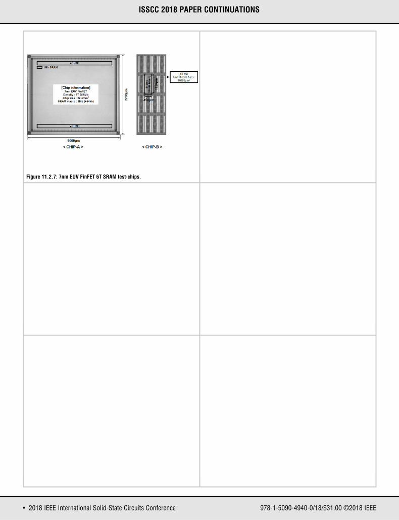
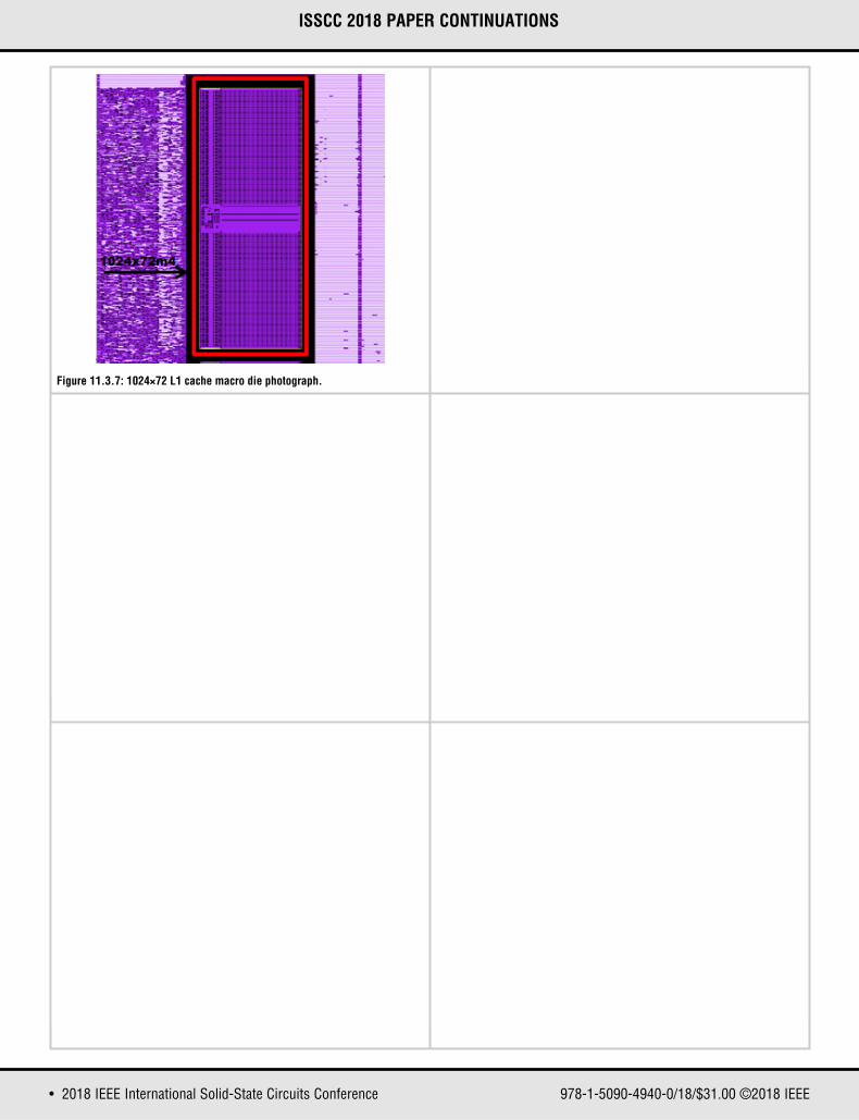
Figure 11.2.6 shows the VMIN distribution of the 7nm EUV FinFET 6T-HD SRAMwith write-assist. The 64 RPB VMIN distribution shows that DWD is expected toimprove VMIN additionally over the operating voltage-range. Figure 11.2.7 showsthe die-photo of the 7nm EUV FinFET SRAM test-chips. Chip-A is designed usinga 256Mb SRAM macro that explores NBL and DWD write-assist schemes. Chip-B is configured using 512Kb SRAM macros using the 0.026μm2 6T-HD bitcell,which shows a VMIN distribution with NBL assist and DWD impact.
References:[1] S. Y. Wu, et al., "Demonstration of a sub-0.03 um2 high density 6-T SRAMwith scaled bulk FinFETs for mobile SOC applications beyond 10nm node," IEEESymp. VLSI Tech., 2016.[2] J. Chang, et al., "A 7nm 256Mb SRAM in high-k metal-gate FinFET technologywith write-assist circuitry for low-VMIN applications," ISSCC, pp. 206-207, 2017.[3] T. Song, et al., "A 7nm FinFET SRAM macro using EUV lithography forperipheral repair analysis," ISSCC, pp. 208-209, 2017.[4] D. Ha, et al., "Highly manufacturable 7nm FinFET technology featuring EUVlithography for low power and high performance applications," IEEE Symp. VLSITech., 2017.[5] T. Song, et al., "A 10nm FinFET 128Mb SRAM with assist adjustment systemfor power, performance, and area optimization," ISSCC, pp. 306-307, 2016 .
Figure 11.2.1: 7nm EUV FinFET 6T HD 0.026 µm2 SRAM bitcell. Figure 11.2.2: EUV design flexibility with smaller IR-drop impact.
Figure 11.2.3: Conventional SRAM assist, and WRM versus rows per BL.
Figure 11.2.5: 256Mb SRAM silicon result with DWD or/and NBL, and SRAMmacro area comparison for write-assist schemes and bank-architectures. Figure 11.2.6: VMIN distribution of 6T-HD SRAM bitcell.
200 • 2018 IEEE International Solid-State Circuits Conference
ISSCC 2018 / SESSION 11 / SRAM / 11.3
11.3 A 5GHz 7nm L1 Cache Memory Compiler for High-Speed Computing and Mobile Applications
Michael Clinton1, Rajinder Singh1, Marty Tsai1, Shayan Zhang1, Bryan Sheffield1, Jonathan Chang2
1TSMC, Austin, TX2TSMC, Hsinchu, Taiwan
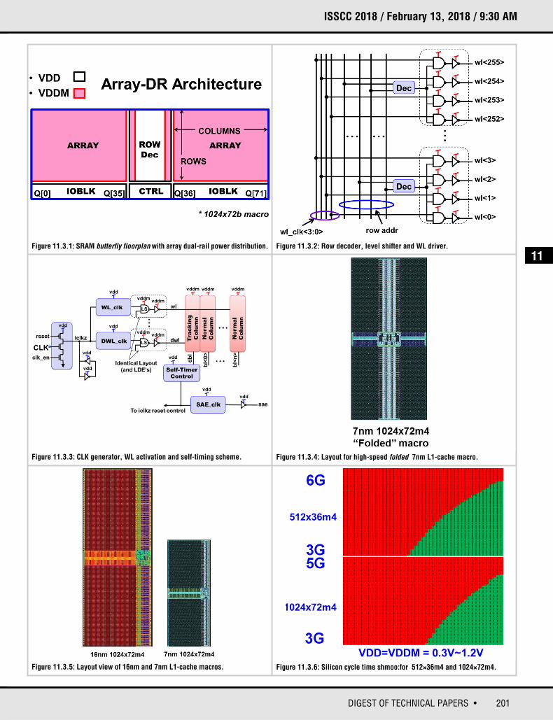
In high performance computing (HPC) applications, the speed of the L1 cachewill typically determine the maximum frequency (fMAX) of the processor core.Companies that mass produce high-performance microprocessors commonlyhave the L1 cache consist of fully-custom macros: to ensure that the performanceof the L1 cache does not limit the fMAX or throughput of the processor. In addition,it is also common for the custom L1 cache designs to use a two-port 8T or a large6T bitcell, along with domino read logic and very short BL [2,3]. These designstradeoff density and area for high performance. This paper presents a differentapproach, one which can satisfy a range of different applications; a memorycompiler that can generate more than 10,000 different high-speed L1 cache macroconfigurations is proposed. The 7nm L1-cache compiler described in this paperuses a high-current (HC) 6T bitcell, which is more area efficient than an 8T bitcell.The HC bitcell, along with small-signal sensing, allows for long BL (256b), leadingto further area efficiency improvements. Since these L1 macros are just as likelyto be used in mobile applications as they are to be used in HPC applications, theywere implemented using the array dual-rail (ADR) architecture [4]. The ADRarchitecture (Fig. 11.3.1) allows the periphery circuits of the L1 macro to operateat the same voltage as the processor core: a lower VDD results in dynamic powersavings. ADR performance is also improved, over an interface dual-rail, when theSRAM and logic supplies are equivalent, as ADR design does not suffer from alevel-shifter delays on the inputs or outputs.
Quickly activating the WL is critical for a high-speed L1 cache. The L1 macro isbuilt using a standard SRAM butterfly architecture and places the row-decoderand WL drivers in the center of the macro, which reduces the WL RC delay by 4×.Due to the increased wiring and via resistance in advanced nodes (i.e. 7nm)careful layout construction is required to guarantee that the upper and lower WL’sare activated at exactly the same time. Within our power, performance and areaconstraints, we found that a four-WL clock-drive scheme resulted in the bestaddress setup, access time and wiring/circuit area optimization (Fig. 11.3.2).Using wider than minimum WL clock (wl_clk<3:0>) wires, and reducing the gateload by a factor of four helped speed up WL activation. In addition, by controllingthe WL pulse width independently for read and write cycles, we are able to shortenthe WL pulse during a write and reduce the dynamic power associated withdummy reads.
In an ADR design, the WL driver must use the bitcell voltage (VDDM) for properbitcell operations. The L1 cache performs voltage level translation from theperiphery’s supply to VDDM using the NAND gate in the WL decode path. The self-timer scheme used in the L1 cache and described in more detail in the nextparagraph, depends on all of the various delays in the normal and self-time pathmatching. In this design we copy the entire 4-WL decode/driver block and use itto activate the single tracking WL. This allows us to replicate the layout contextand layout dependent effects (LDE) for this critical portion of the access path.
The rising edge of CLK generates the internal clock (iclkz) and starts an access tothe L1 cache. The self-timing scheme controls the setting time of the senseamplifier and the timing of the restore sequence. The internal clock has a veryhigh fan-out, but we are able to generate iclkz and drive it with only one gate delayby using a dynamic clock generator circuit (Fig. 11.3.3).
The self-timing scheme consists of tracking bitcells, which are base-layer identicalto normal bitcells, and therefore can track the normal bitcell read current (ICELL)closely. The tracking BL has the same wire and diffusion loading as a normal BL,thus tracking the rate of voltage change very closely and proportionately to therate of differential development on a normal BL. This scheme uses a tracking WLwhich is tuned to match the rise time of a normal WL across the full range ofcolumns of the L1 compiler. The differential on the BL’s at sense time is flat as afunction of columns, which allows us to drive the global IO signals with fast edges.The restore operation start is timed from the sense enable trigger signal, whichhelps to minimize cycle time.
The HC bitcell can meet the performance targets with a 256b long BL, but thereis a significant performance improvement when the BL length is cut in half. Thisis exactly what is done with what we refer to as the folded option. For this option,we fold the L1 macro over its right edge and reduce the BL length in half(Fig. 11.3.4). The capacity of the macro remains the same, but the BL length ishalved leading to a 15-20% reduction in access and cycle time. In our currentimplementation of the folded macro, the area penalty is approximately 15%. Thefolding option can offer a sufficient performance boost, for example by pushingthe minimum cycle time of the largest macro (72kb) to over 5GHz.
We recognize that the minimum differential, even with a 6σ weak bitcell, increasesas the SRAM bitcell voltage is increased. We take advantage of this fact by offeringa turbo mode at higher voltages, where the sense enable timing is advanced.Putting the largest L1 macros into turbo mode at high voltage, can result in anadditional 5% performance boost.
Compared to a 16nm L1 cache [5] that uses the same architecture, the presented7nm cache is over 60% smaller (Fig. 11.3.5). The high-speed 7nm L1-cachecomplier described in this paper has been verified in silicon. Cycle timemeasurements made at room temperature and -40°C are presented for a 512×36and a 1024×72 macro. The measured results were performed on a slow-cornerlot.. The -40°C measured results show that the 18kb macro is able to run at5.36GHz at 1.115V, while the largest 72kb macro is able to achieve 4.4GHzoperation at this voltage (Fig. 11.3.6).
The authors would like to thank Van Sisourath for physical design support, andRao Kodali for logic verification.
References:[1] J. Chang, et al., “A 7nm 256Mb SRAM in High-K Metal-Gate FinFETTechnology with Write-Assist Circuitry fo Low-VMIN Applications,” ISSCC, pp. 206-207, 2017.[2] J. Davis, et al., “7GHz L1 Cache SRAMs for the 32nm zEnterprise EC12Processor,” ISSCC, pp. 324-325, 2013.[3] J. Kulkarni, et al., “Dual-Vcc 8T-bitcell SRAM Array in 22nm Tri-Gate CMOSfor Energy-Efficient Operation across Wide Dynamic Voltage Range,” IEEE Symp.VLSI Tech., pp. 126-127, 2013.[4] M. Clinton, et al., “A Low-Power and High-Performance 10nm Architecturefor Mobile Applications,” ISSCC, pp. 210-211, 2017.[5] J. Chang, et al., “Embedded Memories for Mobile, IoT, Automotive and HighPerformance Computing,” IEEE Symp. VLSI Tech., pp. 26-27, 2017.