1037
Hitachi SuperH RISC engine SH7750 Series SH7750, SH7750S, SH7750R Hardware Manual ADE-602-124E Rev. 6.0 7/10/2002 Hitachi, Ltd.

Hitachi SuperH RISC engine
SH7750 Series
SH7750, SH7750S, SH7750R
Hardware Manual
ADE-602-124E
Rev. 6.07/10/2002Hitachi, Ltd.

Cautions
1. Hitachi neither warrants nor grants licenses of any rights of Hitachi’s or any third party’spatent, copyright, trademark, or other intellectual property rights for information contained inthis document. Hitachi bears no responsibility for problems that may arise with third party’srights, including intellectual property rights, in connection with use of the informationcontained in this document.
2. Products and product specifications may be subject to change without notice. Confirm that youhave received the latest product standards or specifications before final design, purchase oruse.
3. Hitachi makes every attempt to ensure that its products are of high quality and reliability.However, contact Hitachi’s sales office before using the product in an application thatdemands especially high quality and reliability or where its failure or malfunction may directlythreaten human life or cause risk of bodily injury, such as aerospace, aeronautics, nuclearpower, combustion control, transportation, traffic, safety equipment or medical equipment forlife support.
4. Design your application so that the product is used within the ranges guaranteed by Hitachiparticularly for maximum rating, operating supply voltage range, heat radiation characteristics,installation conditions and other characteristics. Hitachi bears no responsibility for failure ordamage when used beyond the guaranteed ranges. Even within the guaranteed ranges,consider normally foreseeable failure rates or failure modes in semiconductor devices andemploy systemic measures such as fail-safes, so that the equipment incorporating Hitachiproduct does not cause bodily injury, fire or other consequential damage due to operation ofthe Hitachi product.
5. This product is not designed to be radiation resistant.
6. No one is permitted to reproduce or duplicate, in any form, the whole or part of this documentwithout written approval from Hitachi.
7. Contact Hitachi’s sales office for any questions regarding this document or Hitachisemiconductor products.

Rev. 6.0, 07/02, page iii of I
Preface
The SH-4 (SH7750 Series: SH7750, SH7750S, SH7750R) microprocessor incorporates the 32-bitSH-4 CPU and is also equipped with peripheral functions necessary for configuring a user system.
The SH7750 Series is built in with a variety of peripheral functions such as cache memory,memory management unit (MMU), interrupt controller, timers, two serial communicationinterfaces (SCI, SCIF), real-time clock (RTC), user break controller (UBC), bus state controller(BSC) and smart card interface. This series can be used in a wide range of multimedia equipment.The bus controller is compatible with ROM, SRAM, DRAM, synchronous DRAM and PCMCIA,as well as 64-bit synchronous DRAM 4-bank system and 64-bit data bus.
Target Readers: This manual is designed for use by people who design application systems usingthe SH7750, SH7750S, or SH7750R.To use this manual, basic knowledge of electric circuits, logic circuits and microcomputers isrequired.
Purpose: This manual provides the information of the hardware functions and electricalcharacteristics of the SH7750, SH7750S, and SH7750R.The SH-4 Programming Manual contains detailed information of executable instructions. Pleaseread the Programming Manual together with this manual.
How to Use the Book:• To understand general functions
→ Read the manual from the beginning.
The manual explains the CPU, system control functions, peripheral functions and electricalcharacteristics in that order.
• To understanding CPU functions
→ Refer to the separate SH-4 Programming Manual.
Explanatory Note: Bit sequence: upper bit at left, and lower bit at right
List of Related Documents: The latest documents are available on our Web site. Please makesure that you have the latest version.(http://www.hitachisemiconductor.com/)
• User manuals for SH7750, SH7750S, and SH7750R
Name of Document Document No.
SH7750 Series Hardware Manual This manual
SH-4 Programming Manual ADE-602-156

Rev. 6.0, 07/02, page iv of I
• User manuals for development tools
Name of Document Document No.
C/C++ Compiler, Assembler, Optimizing Linkage Editor User’s Manual ADE-702-246
Simulator/Debugger User’s Manual ADE-702-186
Hitachi Embedded Workshop User’s Manual ADE-702-201

Rev. 6.0, 07/02, page v of I
List of Items Revised or Added for This Version
Section Page Item Description
1.1 SH7750 Series (SH7750,SH7750S, SH7750R)Features
1 Description amendedand added
4 to 8 Table 1.1 SH7750 SeriesFeatures
Description added forLSI, and descriptionand Note added forClock pulse generator(CPG)
SH7750 and SH7750Sadded to cache memory
Cache memory[SH7750R] added totable
Description added forDirect memory accesscontroller (DMAC) andTimer unit (TMU)
SH7750R table addedto Product lineup
Notes 1, 2, 3 added
1.2 Block Diagram 9 Figure 1.1 Block Diagram ofSH7750 Series Functions
I cache 8 KB and 0cache 16 KB deletedfrom table
1.3 Pin Arrangement 10 to 12 Figure 1.2 to 1.4 SH7750R added, anddescription amended
1.4 Pin Functions 13 to 40 Table 1.2 to 1.4 Table and noteamended
2.7 Processor Modes 55 Description deleted
3.2 Register Descriptions 61 Figure 3.2 MMU-RelatedRegisters
Amended
62 3. Page table entryassistance register (PTEA)
SH7750R added afterSH7750S
62 1. Page table entry highregister (PTEH),6. MMU control register(MMUCR)
Description added
3.3.1 Physical AddressSpace
64 to 67 Description added
Rev. 6.0, 07/02, page vi of I
Section Page Item Description
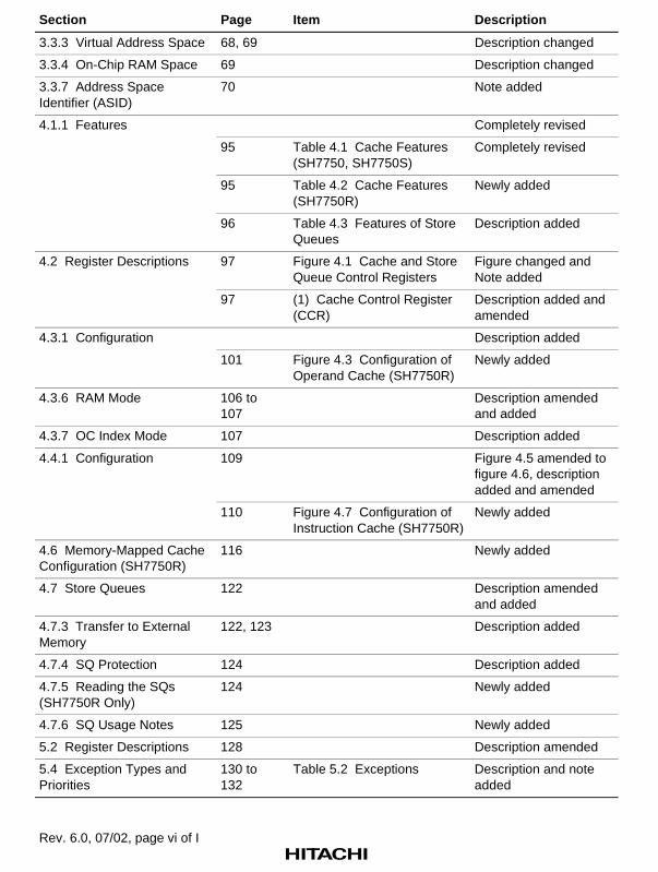
3.3.3 Virtual Address Space 68, 69 Description changed
3.3.4 On-Chip RAM Space 69 Description changed
3.3.7 Address SpaceIdentifier (ASID)
70 Note added
4.1.1 Features Completely revised
95 Table 4.1 Cache Features(SH7750, SH7750S)
Completely revised
95 Table 4.2 Cache Features(SH7750R)
Newly added
96 Table 4.3 Features of StoreQueues
Description added
4.2 Register Descriptions 97 Figure 4.1 Cache and StoreQueue Control Registers
Figure changed andNote added
97 (1) Cache Control Register(CCR)
Description added andamended
4.3.1 Configuration Description added
101 Figure 4.3 Configuration ofOperand Cache (SH7750R)
Newly added
4.3.6 RAM Mode 106 to107
Description amendedand added
4.3.7 OC Index Mode 107 Description added
4.4.1 Configuration 109 Figure 4.5 amended tofigure 4.6, descriptionadded and amended
110 Figure 4.7 Configuration ofInstruction Cache (SH7750R)
Newly added
4.6 Memory-Mapped CacheConfiguration (SH7750R)
116 Newly added
4.7 Store Queues 122 Description amendedand added
4.7.3 Transfer to ExternalMemory
122, 123 Description added
4.7.4 SQ Protection 124 Description added
4.7.5 Reading the SQs(SH7750R Only)
124 Newly added
4.7.6 SQ Usage Notes 125 Newly added
5.2 Register Descriptions 128 Description amended
5.4 Exception Types andPriorities
130 to132
Table 5.2 Exceptions Description and noteadded
Rev. 6.0, 07/02, page vii of I
Section Page Item Description
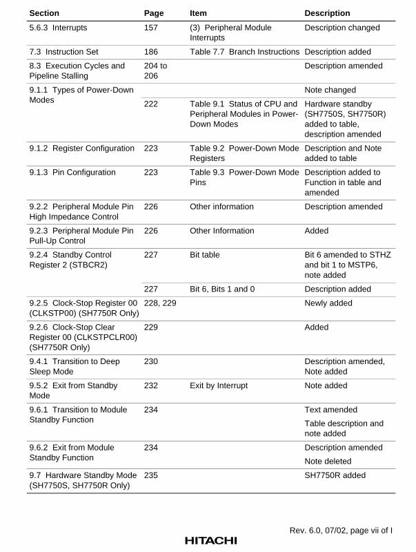
5.6.3 Interrupts 157 (3) Peripheral ModuleInterrupts
Description changed
7.3 Instruction Set 186 Table 7.7 Branch Instructions Description added
8.3 Execution Cycles andPipeline Stalling
204 to206
Description amended
Note changed9.1.1 Types of Power-DownModes 222 Table 9.1 Status of CPU and
Peripheral Modules in Power-Down Modes
Hardware standby(SH7750S, SH7750R)added to table,description amended
9.1.2 Register Configuration 223 Table 9.2 Power-Down ModeRegisters
Description and Noteadded to table
9.1.3 Pin Configuration 223 Table 9.3 Power-Down ModePins
Description added toFunction in table andamended
9.2.2 Peripheral Module PinHigh Impedance Control
226 Other information Description amended
9.2.3 Peripheral Module PinPull-Up Control
226 Other Information Added
9.2.4 Standby ControlRegister 2 (STBCR2)
227 Bit table Bit 6 amended to STHZand bit 1 to MSTP6,note added
227 Bit 6, Bits 1 and 0 Description added
9.2.5 Clock-Stop Register 00(CLKSTP00) (SH7750R Only)
228, 229 Newly added
9.2.6 Clock-Stop ClearRegister 00 (CLKSTPCLR00)(SH7750R Only)
229 Added
9.4.1 Transition to DeepSleep Mode
230 Description amended,Note added
9.5.2 Exit from StandbyMode
232 Exit by Interrupt Note added
9.6.1 Transition to ModuleStandby Function
234 Text amended
Table description andnote added
9.6.2 Exit from ModuleStandby Function
234 Description amended
Note deleted
9.7 Hardware Standby Mode(SH7750S, SH7750R Only)
235 SH7750R added

Rev. 6.0, 07/02, page viii of I
Section Page Item Description
9.8.5 Hardware StandbyMode Timing (SH7750S,SH7750R Only)
244 to246
Figures 9.12, 9.13, 9.15 Figures changed
Notes added
10.2.1 Block Diagram ofCPG
249 Figure 10.1 (1) BlockDiagram of CPG (SH7750,SH7750S)
Amended
250 Figure 10.1 (2) BlockDiagram of CPG (SH7750R)
Newly added
10.2.2 CPG PinConfiguration
252 Table 10.1 CPG Pins Table and Noteamended
10.2.3 CPG RegisterConfiguration
252 Table 10.2 CPG Register Description added
10.3 Clock Operating Modes Description added andamended
253 Table 10.3 (1) ClockOperating Modes (SH7750,SH7750S)
Table amended andNote amended andadded
253 Table 10.3 (2) ClockOperating Modes (SH7750R)
Newly added
254 Table 10.4 FRQCR Settingsand Internal ClockFrequencies
Table and Noteamended
10.8.2 Watchdog TimerControl/Status Register(WTCSR)
261 Description amended
10.10 Notes on BoardDesign
265 When Using a PLL OscillatorCircuit
Description amended
266 Figure 10.5 Points forAttention when Using PLLOscillator Circuit
Amended
11.1.1 Features 267 Description added forAlarm interrupts
11.1.2 Block Diagram 268 Figure 11.1 Block Diagramof RTC
Figure amended andNote added
11.1.3 Pin Configuration 269 Table 11.1 RTC Pins Table amended
11.1.4 Register Configuration 270 Table 11.2 RTC Registers RTC control register 3and Year alarm registeradded to table, andNote added

Rev. 6.0, 07/02, page ix of I
Section Page Item Description
11.2.2 Second Counter(RSECCNT)
271 Description amended
11.2.17 RTC ControlRegister 3 (RCR3) and Year-Alarm Register (RYRAR)(SH7750R Only)
283 Newly added
11.3.3 Alarm Function 288 Description added
11.5.2 Carry Flag andInterrupt Flag in StandbyMode
289 Added
11.5.3 Crystal OscillatorCircuit
290 Figure 11.5 Example ofCrystal Oscillator CircuitConnection
Note amended
12.1.1 Features 291 Description amendedand added
12.1.2 Block Diagram 292 Figure 12.1 Block Diagram of TMU,amended
12.1.4 Register Configuration 293,294
Table 12.2 TMU Registers Description and Noteadded
12.2.3 Timer Start Register2 (TSTR2)
297 Added
12.2.4 Timer ConstantRegisters (TCOR)
298 Description amendedand added
12.2.5 Timer Counters(TCNT)
298,299
Description amendedand added
12.2.6 Timer ControlRegisters (TCR)
299 Description amendedand added
12.3.1 Counter Operation 304 Description added
12.4 Interrupts 308 Description amendedand added
309 Table 12.3 TMU InterruptSources
Channels 3 and 4added to table
Note added
13.1.1 Features 312 Burst ROM interface Description amendedand added, and Noteadded
13.1.2 Block Diagram 313 Figure 13.1 Block Diagramof BSC
Figure amended andadd Note added

Rev. 6.0, 07/02, page x of I
Section Page Item Description
13.1.4 Register Configuration 318 Table 13.2 BSC Registers Bus control register 3and 4 added to table,and Note added
13.1.5 Overview of Areas 320 Table 13.3 External MemorySpace Map
64*7 added to Area 0, 5,6 Settable Bus Widths,and Note 7 added
319 Space Divisions Description amended
320 Table 13.3 External MemorySpace Map
Table amended, andNotes amended andadded
321, 322 Memory Bus Width Description added
13.2.1 Bus Control Register1 (BCR1)
326 Bit table Bit 18 amended andnote added
327 Bit 31, Bit 30, Bit 29 Description added
328 Bit 26
330 Bit 16
Description and notesadded
330 Bit 15, Bit 14 Description amended
331 Bits 13 to 11
332 Bits 10 to 8
333 Bits 7 to 5
Table amended andnote added
334 Bit 0 Description amended
13.2.2 Bus Control Register2 (BCR2)
335 Bits 15, 14 Description added
337 Newly added13.2.3 Bus Control Register3 (BCR3) (SH7750R Only) 338 Bits 12 to 1—Reserved Description added
13.2.4 Bus Control Register4 (BCR4)
338,339
Newly added
13.2.5 Wait Control Register1 (WCR1)
342 Note amended
13.2.6 Wait Control Register2 (WCR2)
344 to349
Bits 31 to 29, Bits 25 to 23,Bits 19 to 17, Bits 15 to 13,Bits 11 to 9, Bits 8 to 6,Bits 5 to 3, and Bits 2 to 0
Description added andamended
13.2.7 Wait Control Register3 (WCR3)
351 Bit table Bits 19 and 7 changed,and Note added
351 Description added

Rev. 6.0, 07/02, page xi of I
Section Page Item Description
13.2.8 Memory ControlRegister (MCR)
355 Bits 15 to 13—WritePrecharge Delay (TRWL2–TRWL0)
Description added
358 For Synchronous DRAMInterface
AMX6 description andNotes amended
13.2.10 Synchronous DRAMMode Register (SDMR)
362 to364
Description amended,and Note added
370 Description amended13.3.1 Endian/Access Sizeand Data Alignment 371 Data Configuration Quadword partially
amended
13.3.2 Areas 382 Area 0, Area 1 Description added andamended
13.3.3 SRAM Interface 387 Basic interface changedto SRAM interface
387 Basic Timing Description amended
388, 393to 395
Figures 13.6, 13.11 to 13.13 Notes added
395 Read-Strobe Negate Timing(Setting Only Possible in theSH7750R)
Description added andamended
13.3.4 DRAM Interface 400 to 408 Figures 13.17 to 13.22 Notes added
13.3.5 Synchronous DRAMInterface
413 Connection of SynchronousDRAM
Description added
415 Address Multiplexing Description amended
417 to428
Figure 13.28 to 13.37 Note added
435 Power-On Sequence Newly added
438 Notes on Changing the BurstLength (Variation OnlyPossible in the SH7750R)
Newly added
440 Connecting a 128-Mbit/256-Mbit Synchronous DRAM with64-bit Bus Width
Newly added
13.3.6 Burst ROM Interface 441, 442 Description amended
442 to 444 Figure 13.46 to 13.48 Notes added

Rev. 6.0, 07/02, page xii of I
Section Page Item Description
13.3.7 PCMCIA Interface 444, 445 Description amendedand added
446 Table 13.18 Relationshipbetween Address and CEwhen Using PCMCIAInterface
Table amended
449, 452to 454
Figures 13.50, 13.53 to 13.55 Notes added
450 Figure 13.51 Wait Timing forPCMCIA Memory CardInterface
SH7750R added toNote
451 Figure 13.52 PCMCIA SpaceAllocation
Amended
13.3.8 MPX Interface 455 Description added andamended
471 Figure 13.71 MPX InterfaceTiming 7
Amended
457 to 472 Figures 13.57 to 13.72 Notes added
473 Description amended13.3.9 Byte Control SRAMInterface 475 to 477 Figures 13.74 to 13.76 Notes added
13.3.10 Waits betweenAccess Cycles
479 Figure 13.77 Waits betweenAccess Cycles
Replaced
13.3.11 Bus Arbitration 480, 481 Description added andamended
13.3.16 Notes on Usage 487 Refresh, Bus Arbitration Description amended
487 Synchronous DRAM ModeRegister Setting (SH7750,SH7750R Only)
Newly added
14.1 Overview 489 Description added andamended
14.1.1 Features 489 to 491 Description amended
492 Title amended14.1.2 Block Diagram(SH7750, SH7750S) 492 Figure 14.1 Block Diagram
of DMACAmended
14.2 Register Descriptions(SH7750, SH7750S)
496 Title amended

Rev. 6.0, 07/02, page xiii of I
Section Page Item Description
14.2.1 DMA Source AddressRegisters 0–3 (SAR0–SAR3)
496 Description amended
14.2.2 DMA DestinationAddress Registers 0–3(DAR0–DAR3)
497 Description amended
14.2.3 DMA Transfer CountRegisters 0–3 (DMATCR0–DMATCR3)
498 Description amended
499 Description of DDTmode added
502, 503 Bits 19 to 16 Initial value changed
503 Bits 15, 14 and Bits 13, 12 Description amended
14.2.4 DMA Channel ControlRegisters 0–3 (CHCR0–CHCR3)
505 Bits 6 to 4 Description added
14.2.5 DMA OperationRegister (DMAOR)
508 Bit 4 Description amended
14.3.2 DMA TransferRequests
513 • External RequestAcceptance Conditions
Description added
14.3.4 Types of DMATransfer
526 Table 14.9 External RequestTransfer Sources andDestinations in DDT Mode
Usable DMAC channelschanged
525 (a) Normal DMA Mode Description amendment
14.3.5 Number of Bus CycleStates and DREQ PinSampling Timing
533 to535
Figure 14.15 to 14.17 Figure descriptionadded
14.5 On-Demand DataTransfer Mode (DDT Mode)
545 Descriptionamendments
14.5.2 Pins in DDT Mode 547 BAVL: Data bus D63–D0release signal
Description added
551, 552 Figures 14.26, 14.27 Title amended14.5.3 Transfer RequestAcceptance on Each Channel 553 Figure 14.28 Newly added
554 Figure 14.29 Amended
554, 555 Figure 14.30, 14.31 Errors corrected
14.5.4 Notes on Use of DDTModule
572 c. of 3. Handshake protocolusing the data bus (valid onchannel 0 only)
Description amended
573 b. of 8. Data transfer endrequest
Added
573 12. Confirming DMA transferrequests and number oftransfers executed
Description amended

Rev. 6.0, 07/02, page xiv of I
Section Page Item Description
14.6 Configuration of theDMAC (SH7750R)
574 Newly added
14.7 Register Descriptions(SH7750R)
579 Newly added
14.8 Operation (SH7750R) 586 Added
14.9 Usage Notes 591 4. Description amended
592 9. Newly added
15.2.8 Serial Port Register(SCSPTR1)
609 Bit 7 Description amended
16.1.2 Block Diagram 659 Figure 16.1 Block Diagramof SCIF
Amended
16.1.3 Pin Configuration 660 Table 16.1 SCIF Pins Note changed
16.2.6 Serial ControlRegister (SCSCR2)
667 Bit 1 Description amended
16.2.7 Serial Status Register(SCFSR2)
669 Bit 7—Receive Error (ER) Note descriptionchanged
672 Bit 3—Framing Error (FER) Description changed
672 Bit 2—Parity Error (PER) Description changed
16.2.9 FIFO Control Register(SCFCR2)
676 Bits 10 to 8 SH7750R added
16.2.11 Serial Port Register(SCSPTR2)
Figure 16.6 MRESET/SCK2Pin
Deleted
16.3.2 Serial Operation 689 Figure 16.6 Sample SCIFInitialization Flowchart
Amended
696 Serial Data Reception Description added to 5.
17.1 Overview 703 Description amended
17.3.2 Pin Connections 711 Description deleted
18.1.3 Pin Configuration 740 Table 18.3 SCIF I/O PortPins
Amended
19.1.2 Block Diagram 752 Figure 19.1 Block Diagramof INTC
Amended
19.1.4 Register Configuration 753 Table 19.2 INTC Registers Description added totable, Notes added andamended
19.2.3 On-Chip PeripheralModule Interrupts
757, 758 Description added andamended
Rev. 6.0, 07/02, page xv of I
Section Page Item Description
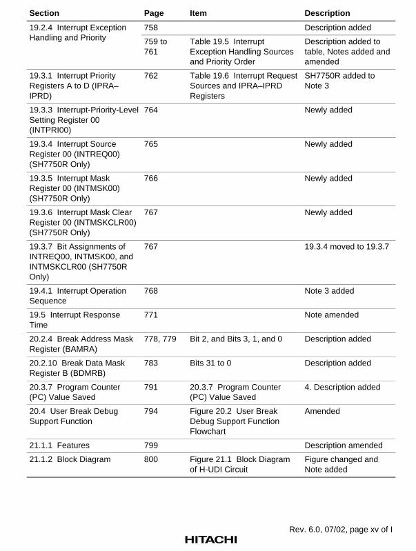
758 Description added19.2.4 Interrupt ExceptionHandling and Priority 759 to
761Table 19.5 InterruptException Handling Sourcesand Priority Order
Description added totable, Notes added andamended
19.3.1 Interrupt PriorityRegisters A to D (IPRA–IPRD)
762 Table 19.6 Interrupt RequestSources and IPRA–IPRDRegisters
SH7750R added toNote 3
19.3.3 Interrupt-Priority-LevelSetting Register 00(INTPRI00)
764 Newly added
19.3.4 Interrupt SourceRegister 00 (INTREQ00)(SH7750R Only)
765 Newly added
19.3.5 Interrupt MaskRegister 00 (INTMSK00)(SH7750R Only)
766 Newly added
19.3.6 Interrupt Mask ClearRegister 00 (INTMSKCLR00)(SH7750R Only)
767 Newly added
19.3.7 Bit Assignments ofINTREQ00, INTMSK00, andINTMSKCLR00 (SH7750ROnly)
767 19.3.4 moved to 19.3.7
19.4.1 Interrupt OperationSequence
768 Note 3 added
19.5 Interrupt ResponseTime
771 Note amended
20.2.4 Break Address MaskRegister (BAMRA)
778, 779 Bit 2, and Bits 3, 1, and 0 Description added
20.2.10 Break Data MaskRegister B (BDMRB)
783 Bits 31 to 0 Description added
20.3.7 Program Counter(PC) Value Saved
791 20.3.7 Program Counter(PC) Value Saved
4. Description added
20.4 User Break DebugSupport Function
794 Figure 20.2 User BreakDebug Support FunctionFlowchart
Amended
21.1.1 Features 799 Description amended
21.1.2 Block Diagram 800 Figure 21.1 Block Diagramof H-UDI Circuit
Figure changed andNote added

Rev. 6.0, 07/02, page xvi of I
Section Page Item Description
21.1.3 Pin Configuration 801 Table 21.1 H-UDI Pins Table amended andNote 3 added
21.1.4 Register Configuration 802 Table 21.2 H-UDI Registers Description added totable and Notes 3 and 4added
21.2.1 Instruction Register(SDIR)
804 [SH7750R] descriptionadded
21.2.4 Interrupt SourceRegister (SDINT)
806 Newly added
21.2.5 Boundary ScanRegister (SDBSR)
806 Newly added
808, 809 Table 21.3 Configuration ofthe Boundary Scan Register(2), (3)
Newly added
21.3.3 H-UDI Interrupt 811 Description changed
21.3.4 BYPASS Deleted
21.3.4 Boundary Scan(EXTEST, SAMPLE/PRELOAD, BYPASS)
812 Newly added
21.4 Usage Notes 812 5. Description added
22.1 Absolute MaximumRatings
813 Table 22.1 AbsoluteMaximum Ratings
Table amended andnotes amended
22.2 DC Characteristics 814, 815 Table 22.2DC Characteristics(HD6417750RBP240)
Newly added
816, 817 Table 22.3DC Characteristics(HD6417750RF240)
Newly added
818, 819 Table 22.4DC Characteristics(HD6417750RBP200)
Newly added
820, 821 Table 22.5DC Characteristics(HD6417750RF200)
Newly added
822, 823 Table 22.6DC Characteristics(HD6417750SBP200)
Amended
826, 827 Table 22.8DC Characteristics(HD6417750BP200M)
Amended
Rev. 6.0, 07/02, page xvii of I
Section Page Item Description
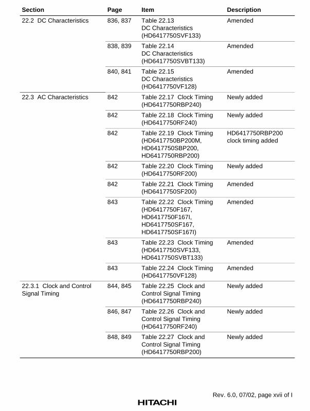
22.2 DC Characteristics 836, 837 Table 22.13DC Characteristics(HD6417750SVF133)
Amended
838, 839 Table 22.14DC Characteristics(HD6417750SVBT133)
Amended
840, 841 Table 22.15DC Characteristics(HD6417750VF128)
Amended
22.3 AC Characteristics 842 Table 22.17 Clock Timing(HD6417750RBP240)
Newly added
842 Table 22.18 Clock Timing(HD6417750RF240)
Newly added
842 Table 22.19 Clock Timing(HD6417750BP200M,HD6417750SBP200,HD6417750RBP200)
HD6417750RBP200clock timing added
842 Table 22.20 Clock Timing(HD6417750RF200)
Newly added
842 Table 22.21 Clock Timing(HD6417750SF200)
Amended
843 Table 22.22 Clock Timing(HD6417750F167,HD6417750F167I,HD6417750SF167,HD6417750SF167I)
Amended
843 Table 22.23 Clock Timing(HD6417750SVF133,HD6417750SVBT133)
Amended
843 Table 22.24 Clock Timing(HD6417750VF128)
Amended
22.3.1 Clock and ControlSignal Timing
844, 845 Table 22.25 Clock andControl Signal Timing(HD6417750RBP240)
Newly added
846, 847 Table 22.26 Clock andControl Signal Timing(HD6417750RF240)
Newly added
848, 849 Table 22.27 Clock andControl Signal Timing(HD6417750RBP200)
Newly added

Rev. 6.0, 07/02, page xviii of I
Section Page Item Description
22.3.1 Clock and ControlSignal Timing
850, 851 Table 22.28 Clock andControl Signal Timing(HD6417750RF200)
Newly added
852, 853 Table 22.29 Clock andControl Signal Timing(HD6417750BP200M,HD6417750SBP200)
Newly added
854, 855 Table 22.30 Clock andControl Signal Timing(HD6417750SF200)
Amended
856, 857 Table 22.31 Clock andControl Signal Timing(HD6417750F167,HD6417750F167I,HD6417750SF167,HD6417750SF167I)
Amended
858, 859 Table 22.32 Clock andControl Signal Timing(HD6417750SVF133,HD6417750SVBT133)
Amended
860, 861 Table 22.33 Clock andControl Signal Timing(HD6417750VF128)
Amended
864 Figure 22.6 Standby ReturnOscillation Settling Time(Return by RESET)
Amended
865 Figure 22.8 Standby ReturnOscillation Settling Time(Return by IRL3–IRL0)
Amended
866 Figure 22.10 PLLSynchronization Settling Timein Case of IRL Interrupt
Amended
22.3.2 Control Signal Timing 868 Table 22.34 Control SignalTiming (1)
Table newly added
22.3.3 Bus Timing 880 Figure 22.18 SRAM BusCycle: Basic Bus Cycle (NoWait, Address Setup/HoldTime Insertion, AnS = 1,AnH = 1)
Figure changed andNote added
881 Figure 22.19 Burst ROMBus Cycle (No Wait)
Amended
871, 872 Table 22.35 Bus Timing (1) Table newly added

Rev. 6.0, 07/02, page xix of I
Section Page Item Description
22.3.4 Peripheral ModuleSignal Timing
924, 925 Table 22.36 PeripheralModule Signal Timing (1)
Table newly added
900 to921, 923
Figures 22.37 to 22.58,Figure 22.60
Titles amended
930 Figure 22.62 RTC OscillationSettling Time at Power-On
Amended
932 Figure 22.66(b) DBREQ/TRInput Timing and BAVLOutput Timing
Newly added
Appendix A Address List 937 to942
Table A.1 Address List BCR4, RCR3, RYRAR,SDINT and Notesadded
BCR3 area 7 addressamended
DMAC, INTC, CPG,TMU table added
Appendix B PackageDimensions
943, 944 Figure B.1 PackageDimensions (256-Pin BGA)
Figure B.2 PackageDimensions (208-Pin QFP)
Amended
Appendix C Mode PinSettings
946 Clock Modes Table 10.3 (1), (2)inserted
947 Area 0 Bus Width Area 0 memory typedeleted and dataintegrated into area 0bus width table
Appendix D CKIO2ENB PinConfiguration
948 Figure D.1 CKIO2ENB PinConfiguration
Amended
Appendix E Pin Functions 950 to952
Table E.1 Pin States inReset, Power-Down State,and Bus-Released State
Sleep row deleted
D40–D51 deleted
Notes added
Appendix F SynchronousDRAM AddressMultiplexing Tables
970, 971 (17) BUS 64(128M: 4M × 8b × 4) × 8(SH7750R only)
(18) BUS 64(256M: 4M × 16b × 4) × 4(SH7750R only)
Newly added

Rev. 6.0, 07/02, page xx of I
Section Page Item Description
Appendix F SynchronousDRAM AddressMultiplexing Tables
972, 973 (19) BUS 32(128M: 4M × 8b × 4) × 4(SH7750S and SH7750Ronly)
(20) BUS 32(256M: 4M × 16b × 4) × 2(SH7750S and SH7750Ronly)
SH7750R added
Appendix H Power-On andPower-Off Procedures
977 to979
Newly added
Appendix I Product CodeLineup
980 Table I.1 SH7750 SeriesProduct Code Lineup
SH7750R added

Rev. 6.0, 07/02, page xxi of I
Contents
Section 1 Overview........................................................................................................... 11.1 SH7750 Series (SH7750, SH7750S, SH7750R) Features................................................. 11.2 Block Diagram.................................................................................................................. 91.3 Pin Arrangement ............................................................................................................... 101.4 Pin Functions .................................................................................................................... 13
1.4.1 Pin Functions (256-Pin BGA).............................................................................. 131.4.2 Pin Functions (208-Pin QFP)............................................................................... 231.4.3 Pin Functions (264-Pin CSP) ............................................................................... 31
Section 2 Programming Model ..................................................................................... 412.1 Data Formats..................................................................................................................... 412.2 Register Configuration...................................................................................................... 42
2.2.1 Privileged Mode and Banks ................................................................................. 422.2.2 General Registers ................................................................................................. 452.2.3 Floating-Point Registers....................................................................................... 472.2.4 Control Registers ................................................................................................. 492.2.5 System Registers.................................................................................................. 50
2.3 Memory-Mapped Registers............................................................................................... 522.4 Data Format in Registers................................................................................................... 532.5 Data Formats in Memory .................................................................................................. 532.6 Processor States ................................................................................................................ 542.7 Processor Modes ............................................................................................................... 55
Section 3 Memory Management Unit (MMU)......................................................... 573.1 Overview........................................................................................................................... 57
3.1.1 Features................................................................................................................ 573.1.2 Role of the MMU................................................................................................. 573.1.3 Register Configuration......................................................................................... 603.1.4 Caution................................................................................................................. 60
3.2 Register Descriptions ........................................................................................................ 613.3 Address Space................................................................................................................... 64
3.3.1 Physical Address Space ....................................................................................... 643.3.2 External Memory Space....................................................................................... 673.3.3 Virtual Address Space.......................................................................................... 683.3.4 On-Chip RAM Space........................................................................................... 693.3.5 Address Translation ............................................................................................. 693.3.6 Single Virtual Memory Mode and Multiple Virtual Memory Mode ................... 703.3.7 Address Space Identifier (ASID) ......................................................................... 70
3.4 TLB Functions .................................................................................................................. 71

Rev. 6.0, 07/02, page xxii of I
3.4.1 Unified TLB (UTLB) Configuration ................................................................... 713.4.2 Instruction TLB (ITLB) Configuration................................................................ 753.4.3 Address Translation Method................................................................................ 75
3.5 MMU Functions................................................................................................................ 783.5.1 MMU Hardware Management ............................................................................. 783.5.2 MMU Software Management .............................................................................. 783.5.3 MMU Instruction (LDTLB)................................................................................. 783.5.4 Hardware ITLB Miss Handling ........................................................................... 793.5.5 Avoiding Synonym Problems .............................................................................. 80
3.6 MMU Exceptions.............................................................................................................. 813.6.1 Instruction TLB Multiple Hit Exception.............................................................. 813.6.2 Instruction TLB Miss Exception.......................................................................... 823.6.3 Instruction TLB Protection Violation Exception ................................................. 833.6.4 Data TLB Multiple Hit Exception ....................................................................... 843.6.5 Data TLB Miss Exception ................................................................................... 843.6.6 Data TLB Protection Violation Exception........................................................... 853.6.7 Initial Page Write Exception................................................................................ 86
3.7 Memory-Mapped TLB Configuration............................................................................... 873.7.1 ITLB Address Array ............................................................................................ 883.7.2 ITLB Data Array 1............................................................................................... 893.7.3 ITLB Data Array 2............................................................................................... 903.7.4 UTLB Address Array........................................................................................... 903.7.5 UTLB Data Array 1 ............................................................................................. 923.7.6 UTLB Data Array 2 ............................................................................................. 93
Section 4 Caches................................................................................................................ 954.1 Overview........................................................................................................................... 95
4.1.1 Features................................................................................................................ 954.1.2 Register Configuration......................................................................................... 96
4.2 Register Descriptions ........................................................................................................ 974.3 Operand Cache (OC)......................................................................................................... 99
4.3.1 Configuration....................................................................................................... 994.3.2 Read Operation .................................................................................................... 1034.3.3 Write Operation ................................................................................................... 1044.3.4 Write-Back Buffer ............................................................................................... 1054.3.5 Write-Through Buffer.......................................................................................... 1054.3.6 RAM Mode.......................................................................................................... 1064.3.7 OC Index Mode ................................................................................................... 1074.3.8 Coherency between Cache and External Memory ............................................... 1074.3.9 Prefetch Operation ............................................................................................... 108
4.4 Instruction Cache (IC)....................................................................................................... 1084.4.1 Configuration....................................................................................................... 1084.4.2 Read Operation .................................................................................................... 111

Rev. 6.0, 07/02, page xxiii of I
4.4.3 IC Index Mode..................................................................................................... 1114.5 Memory-Mapped Cache Configuration (SH7750, SH7750S) .......................................... 112
4.5.1 IC Address Array ................................................................................................. 1124.5.2 IC Data Array....................................................................................................... 1134.5.3 OC Address Array ............................................................................................... 1144.5.4 OC Data Array ..................................................................................................... 115
4.6 Memory-Mapped Cache Configuration (SH7750R)......................................................... 1164.6.1 IC Address Array ................................................................................................. 1174.6.2 IC Data Array....................................................................................................... 1184.6.3 OC Address Array ............................................................................................... 1194.6.4 OC Data Array ..................................................................................................... 1204.6.5 Summary of the Memory-Mapping of the OC..................................................... 121
4.7 Store Queues ..................................................................................................................... 1224.7.1 SQ Configuration................................................................................................. 1224.7.2 SQ Writes............................................................................................................. 1224.7.3 Transfer to External Memory............................................................................... 1224.7.4 SQ Protection....................................................................................................... 1244.7.5 Reading the SQs (SH7750R Only) ...................................................................... 1244.7.6 SQ Usage Notes ................................................................................................... 125
Section 5 Exceptions ........................................................................................................ 1275.1 Overview........................................................................................................................... 127
5.1.1 Features................................................................................................................ 1275.1.2 Register Configuration......................................................................................... 127
5.2 Register Descriptions ........................................................................................................ 1285.3 Exception Handling Functions.......................................................................................... 129
5.3.1 Exception Handling Flow .................................................................................... 1295.3.2 Exception Handling Vector Addresses ................................................................ 129
5.4 Exception Types and Priorities ......................................................................................... 1305.5 Exception Flow ................................................................................................................. 132
5.5.1 Exception Flow.................................................................................................... 1325.5.2 Exception Source Acceptance.............................................................................. 1335.5.3 Exception Requests and BL Bit ........................................................................... 1355.5.4 Return from Exception Handling......................................................................... 135
5.6 Description of Exceptions................................................................................................. 1355.6.1 Resets................................................................................................................... 1365.6.2 General Exceptions .............................................................................................. 1415.6.3 Interrupts.............................................................................................................. 1555.6.4 Priority Order with Multiple Exceptions ............................................................. 158
5.7 Usage Notes ...................................................................................................................... 1595.8 Restrictions ....................................................................................................................... 160

Rev. 6.0, 07/02, page xxiv of I
Section 6 Floating-Point Unit ........................................................................................ 1616.1 Overview........................................................................................................................... 1616.2 Data Formats..................................................................................................................... 161
6.2.1 Floating-Point Format.......................................................................................... 1616.2.2 Non-Numbers (NaN) ........................................................................................... 1636.2.3 Denormalized Numbers ....................................................................................... 164
6.3 Registers............................................................................................................................ 1656.3.1 Floating-Point Registers....................................................................................... 1656.3.2 Floating-Point Status/Control Register (FPSCR)................................................. 1676.3.3 Floating-Point Communication Register (FPUL) ................................................ 168
6.4 Rounding........................................................................................................................... 1686.5 Floating-Point Exceptions................................................................................................. 1696.6 Graphics Support Functions.............................................................................................. 170
6.6.1 Geometric Operation Instructions........................................................................ 1706.6.2 Pair Single-Precision Data Transfer..................................................................... 172
Section 7 Instruction Set ................................................................................................. 1737.1 Execution Environment .................................................................................................... 1737.2 Addressing Modes ............................................................................................................ 1757.3 Instruction Set ................................................................................................................... 179
Section 8 Pipelining.......................................................................................................... 1938.1 Pipelines............................................................................................................................ 1938.2 Parallel-Executability........................................................................................................ 2008.3 Execution Cycles and Pipeline Stalling ............................................................................ 204
Section 9 Power-Down Modes...................................................................................... 2219.1 Overview........................................................................................................................... 221
9.1.1 Types of Power-Down Modes ............................................................................. 2219.1.2 Register Configuration......................................................................................... 2239.1.3 Pin Configuration................................................................................................. 223
9.2 Register Descriptions ........................................................................................................ 2249.2.1 Standby Control Register (STBCR)..................................................................... 2249.2.2 Peripheral Module Pin High Impedance Control................................................. 2269.2.3 Peripheral Module Pin Pull-Up Control............................................................... 2269.2.4 Standby Control Register 2 (STBCR2)................................................................ 2279.2.5 Clock-Stop Register 00 (CLKSTP00) (SH7750R Only) ..................................... 2289.2.6 Clock-Stop Clear Register 00 (CLKSTPCLR00) (SH7750R Only) .................... 229
9.3 Sleep Mode ....................................................................................................................... 2309.3.1 Transition to Sleep Mode..................................................................................... 2309.3.2 Exit from Sleep Mode.......................................................................................... 230
9.4 Deep Sleep Mode.............................................................................................................. 2309.4.1 Transition to Deep Sleep Mode ........................................................................... 230

Rev. 6.0, 07/02, page xxv of I
9.4.2 Exit from Deep Sleep Mode ................................................................................ 2319.5 Standby Mode ................................................................................................................... 231
9.5.1 Transition to Standby Mode................................................................................. 2319.5.2 Exit from Standby Mode...................................................................................... 2329.5.3 Clock Pause Function .......................................................................................... 232
9.6 Module Standby Function................................................................................................. 2339.6.1 Transition to Module Standby Function .............................................................. 2339.6.2 Exit from Module Standby Function ................................................................... 234
9.7 Hardware Standby Mode (SH7750S, SH7750R Only) ..................................................... 2359.7.1 Transition to Hardware Standby Mode................................................................ 2359.7.2 Exit from Hardware Standby Mode ..................................................................... 2359.7.3 Usage Notes ......................................................................................................... 235
9.8 STATUS Pin Change Timing ........................................................................................... 2369.8.1 In Reset ................................................................................................................ 2379.8.2 In Exit from Standby Mode ................................................................................. 2389.8.3 In Exit from Sleep Mode...................................................................................... 2409.8.4 In Exit from Deep Sleep Mode ............................................................................ 2429.8.5 Hardware Standby Mode Timing (SH7750S, SH7750R Only) ........................... 244
Section 10 Clock Oscillation Circuits ........................................................................... 24710.1 Overview........................................................................................................................... 247
10.1.1 Features................................................................................................................ 24710.2 Overview of CPG.............................................................................................................. 249
10.2.1 Block Diagram of CPG........................................................................................ 24910.2.2 CPG Pin Configuration........................................................................................ 25210.2.3 CPG Register Configuration ................................................................................ 252
10.3 Clock Operating Modes .................................................................................................... 25310.4 CPG Register Description................................................................................................. 254
10.4.1 Frequency Control Register (FRQCR)................................................................. 25410.5 Changing the Frequency ................................................................................................... 257
10.5.1 Changing PLL Circuit 1 Starting/Stopping (When PLL Circuit 2 is Off) ........... 25710.5.2 Changing PLL Circuit 1 Starting/Stopping (When PLL Circuit 2 is On) ............ 25710.5.3 Changing Bus Clock Division Ratio (When PLL Circuit 2 is On) ...................... 25810.5.4 Changing Bus Clock Division Ratio (When PLL Circuit 2 is Off)...................... 25810.5.5 Changing CPU or Peripheral Module Clock Division Ratio ............................... 258
10.6 Output Clock Control........................................................................................................ 25810.7 Overview of Watchdog Timer .......................................................................................... 259
10.7.1 Block Diagram..................................................................................................... 25910.7.2 Register Configuration......................................................................................... 260
10.8 WDT Register Descriptions .............................................................................................. 26010.8.1 Watchdog Timer Counter (WTCNT)................................................................... 26010.8.2 Watchdog Timer Control/Status Register (WTCSR)........................................... 26110.8.3 Notes on Register Access..................................................................................... 263

Rev. 6.0, 07/02, page xxvi of I
10.9 Using the WDT................................................................................................................. 26310.9.1 Standby Clearing Procedure ................................................................................ 26310.9.2 Frequency Changing Procedure ........................................................................... 26410.9.3 Using Watchdog Timer Mode ............................................................................. 26410.9.4 Using Interval Timer Mode ................................................................................. 265
10.10 Notes on Board Design ..................................................................................................... 265
Section 11 Realtime Clock (RTC).................................................................................. 26711.1 Overview........................................................................................................................... 267
11.1.1 Features................................................................................................................ 26711.1.2 Block Diagram..................................................................................................... 26811.1.3 Pin Configuration................................................................................................. 26911.1.4 Register Configuration......................................................................................... 269
11.2 Register Descriptions ........................................................................................................ 27111.2.1 64 Hz Counter (R64CNT).................................................................................... 27111.2.2 Second Counter (RSECCNT) .............................................................................. 27111.2.3 Minute Counter (RMINCNT) .............................................................................. 27211.2.4 Hour Counter (RHRCNT).................................................................................... 27211.2.5 Day-of-Week Counter (RWKCNT)..................................................................... 27311.2.6 Day Counter (RDAYCNT) .................................................................................. 27411.2.7 Month Counter (RMONCNT) ............................................................................. 27411.2.8 Year Counter (RYRCNT) .................................................................................... 27511.2.9 Second Alarm Register (RSECAR) ..................................................................... 27611.2.10 Minute Alarm Register (RMINAR) ..................................................................... 27611.2.11 Hour Alarm Register (RHRAR) .......................................................................... 27711.2.12 Day-of-Week Alarm Register (RWKAR)............................................................ 27711.2.13 Day Alarm Register (RDAYAR)......................................................................... 27811.2.14 Month Alarm Register (RMONAR) .................................................................... 27911.2.15 RTC Control Register 1 (RCR1).......................................................................... 27911.2.16 RTC Control Register 2 (RCR2).......................................................................... 28111.2.17 RTC Control Register 3 (RCR3) and Year-Alarm Register (RYRAR)
(SH7750R Only) .................................................................................................. 28311.3 Operation .......................................................................................................................... 285
11.3.1 Time Setting Procedures ...................................................................................... 28511.3.2 Time Reading Procedures .................................................................................... 28611.3.3 Alarm Function .................................................................................................... 288
11.4 Interrupts........................................................................................................................... 28911.5 Usage Notes ...................................................................................................................... 289
11.5.1 Register Initialization........................................................................................... 28911.5.2 Carry Flag and Interrupt Flag in Standby Mode .................................................. 28911.5.3 Crystal Oscillator Circuit ..................................................................................... 289

Rev. 6.0, 07/02, page xxvii of I
Section 12 Timer Unit (TMU)......................................................................................... 29112.1 Overview........................................................................................................................... 291
12.1.1 Features................................................................................................................ 29112.1.2 Block Diagram..................................................................................................... 29212.1.3 Pin Configuration................................................................................................. 29212.1.4 Register Configuration......................................................................................... 293
12.2 Register Descriptions ........................................................................................................ 29512.2.1 Timer Output Control Register (TOCR) .............................................................. 29512.2.2 Timer Start Register (TSTR)................................................................................ 29612.2.3 Timer Start Register 2 (TSTR2) (SH7750R Only) .............................................. 29712.2.4 Timer Constant Registers (TCOR) ...................................................................... 29812.2.5 Timer Counters (TCNT) ...................................................................................... 29812.2.6 Timer Control Registers (TCR) ........................................................................... 29912.2.7 Input Capture Register (TCPR2).......................................................................... 303
12.3 Operation .......................................................................................................................... 30412.3.1 Counter Operation................................................................................................ 30412.3.2 Input Capture Function ........................................................................................ 307
12.4 Interrupts........................................................................................................................... 30812.5 Usage Notes ...................................................................................................................... 309
12.5.1 Register Writes .................................................................................................... 30912.5.2 TCNT Register Reads .......................................................................................... 30912.5.3 Resetting the RTC Frequency Divider................................................................. 30912.5.4 External Clock Frequency.................................................................................... 309
Section 13 Bus State Controller (BSC)......................................................................... 31113.1 Overview........................................................................................................................... 311
13.1.1 Features................................................................................................................ 31113.1.2 Block Diagram..................................................................................................... 31313.1.3 Pin Configuration................................................................................................. 31413.1.4 Register Configuration......................................................................................... 31813.1.5 Overview of Areas ............................................................................................... 31913.1.6 PCMCIA Support ................................................................................................ 322
13.2 Register Descriptions ........................................................................................................ 32613.2.1 Bus Control Register 1 (BCR1) ........................................................................... 32613.2.2 Bus Control Register 2 (BCR2) ........................................................................... 33513.2.3 Bus Control Register 3 (BCR3) (SH7750R Only) ............................................... 33713.2.4 Bus Control Register 4 (BCR4) (SH7750R Only) ............................................... 33813.2.5 Wait Control Register 1 (WCR1)......................................................................... 34013.2.6 Wait Control Register 2 (WCR2)......................................................................... 34313.2.7 Wait Control Register 3 (WCR3)......................................................................... 35113.2.8 Memory Control Register (MCR)........................................................................ 35213.2.9 PCMCIA Control Register (PCR)........................................................................ 35913.2.10 Synchronous DRAM Mode Register (SDMR) .................................................... 362

Rev. 6.0, 07/02, page xxviii of I
13.2.11 Refresh Timer Control/Status Register (RTCSR)................................................ 36413.2.12 Refresh Timer Counter (RTCNT)........................................................................ 36713.2.13 Refresh Time Constant Register (RTCOR) ......................................................... 36813.2.14 Refresh Count Register (RFCR) .......................................................................... 36913.2.15 Notes on Accessing Refresh Control Registers.................................................... 369
13.3 Operation .......................................................................................................................... 37013.3.1 Endian/Access Size and Data Alignment............................................................. 37013.3.2 Areas .................................................................................................................... 38213.3.3 SRAM Interface................................................................................................... 38713.3.4 DRAM Interface .................................................................................................. 39513.3.5 Synchronous DRAM Interface ............................................................................ 41313.3.6 Burst ROM Interface............................................................................................ 44113.3.7 PCMCIA Interface............................................................................................... 44413.3.8 MPX Interface...................................................................................................... 45513.3.9 Byte Control SRAM Interface ............................................................................. 47313.3.10 Waits between Access Cycles.............................................................................. 47813.3.11 Bus Arbitration .................................................................................................... 48013.3.12 Master Mode ........................................................................................................ 48313.3.13 Slave Mode .......................................................................................................... 48413.3.14 Partial-Sharing Master Mode............................................................................... 48513.3.15 Cooperation between Master and Slave............................................................... 48613.3.16 Notes on Usage .................................................................................................... 487
Section 14 Direct Memory Access Controller (DMAC).......................................... 48914.1 Overview........................................................................................................................... 489
14.1.1 Features................................................................................................................ 48914.1.2 Block Diagram (SH7750, SH7750S) ................................................................... 49214.1.3 Pin Configuration (SH7750, SH7750S)............................................................... 49314.1.4 Register Configuration (SH7750, SH7750S)....................................................... 494
14.2 Register Descriptions (SH7750, SH7750S) ...................................................................... 49614.2.1 DMA Source Address Registers 0–3 (SAR0–SAR3) .......................................... 49614.2.2 DMA Destination Address Registers 0–3 (DAR0–DAR3).................................. 49714.2.3 DMA Transfer Count Registers 0–3 (DMATCR0–DMATCR3)......................... 49814.2.4 DMA Channel Control Registers 0–3 (CHCR0–CHCR3)................................... 49914.2.5 DMA Operation Register (DMAOR)................................................................... 507
14.3 Operation .......................................................................................................................... 51014.3.1 DMA Transfer Procedure .................................................................................... 51014.3.2 DMA Transfer Requests ...................................................................................... 51214.3.3 Channel Priorities ................................................................................................ 51514.3.4 Types of DMA Transfer....................................................................................... 51814.3.5 Number of Bus Cycle States and DREQ Pin Sampling Timing .......................... 52714.3.6 Ending DMA Transfer ......................................................................................... 541
14.4 Examples of Use ............................................................................................................... 544
Rev. 6.0, 07/02, page xxix of I
14.4.1 Examples of Transfer between External Memory and an External Devicewith DACK.......................................................................................................... 544
14.5 On-Demand Data Transfer Mode (DDT Mode) ............................................................... 54514.5.1 Operation ............................................................................................................. 54514.5.2 Pins in DDT Mode............................................................................................... 54714.5.3 Transfer Request Acceptance on Each Channel .................................................. 55014.5.4 Notes on Use of DDT Module ............................................................................. 571
14.6 Configuration of the DMAC (SH7750R).......................................................................... 57414.6.1 Block Diagram of the DMAC.............................................................................. 57414.6.2 Pin Configuration (SH7750R) ............................................................................. 57514.6.3 Register Configuration (SH7750R) ..................................................................... 576
14.7 Register Descriptions (SH7750R)..................................................................................... 57914.7.1 DMA Source Address Registers 0–7 (SAR0–SAR7) .......................................... 57914.7.2 DMA Destination Address Registers 0–7 (DAR0–DAR7).................................. 57914.7.3 DMA Transfer Count Registers 0–7 (DMATCR0–DMATCR7)......................... 58014.7.4 DMA Channel Control Registers 0–7 (CHCR0–CHCR7)................................... 58014.7.5 DMA Operation Register (DMAOR)................................................................... 583
14.8 Operation (SH7750R) ....................................................................................................... 58614.8.1 Channel Specification for a Normal DMA Transfer............................................ 58614.8.2 Channel Specification for DDT-Mode DMA Transfer ........................................ 58614.8.3 Transfer Channel Notification in DDT Mode...................................................... 58614.8.4 Clearing Request Queues by DTR Format........................................................... 58714.8.5 Interrupt-Request Codes ...................................................................................... 588
14.9 Usage Notes ...................................................................................................................... 591
Section 15 Serial Communication Interface (SCI) .................................................... 59315.1 Overview........................................................................................................................... 593
15.1.1 Features................................................................................................................ 59315.1.2 Block Diagram..................................................................................................... 59515.1.3 Pin Configuration................................................................................................. 59615.1.4 Register Configuration......................................................................................... 596
15.2 Register Descriptions ........................................................................................................ 59715.2.1 Receive Shift Register (SCRSR1)........................................................................ 59715.2.2 Receive Data Register (SCRDR1) ....................................................................... 59715.2.3 Transmit Shift Register (SCTSR1) ...................................................................... 59815.2.4 Transmit Data Register (SCTDR1)...................................................................... 59815.2.5 Serial Mode Register (SCSMR1)......................................................................... 59915.2.6 Serial Control Register (SCSCR1)....................................................................... 60115.2.7 Serial Status Register (SCSSR1).......................................................................... 60515.2.8 Serial Port Register (SCSPTR1) .......................................................................... 60915.2.9 Bit Rate Register (SCBRR1)................................................................................ 613
15.3 Operation .......................................................................................................................... 62115.3.1 Overview.............................................................................................................. 621

Rev. 6.0, 07/02, page xxx of I
15.3.2 Operation in Asynchronous Mode ....................................................................... 62315.3.3 Multiprocessor Communication Function ........................................................... 63415.3.4 Operation in Synchronous Mode ......................................................................... 642
15.4 SCI Interrupt Sources and DMAC .................................................................................... 65115.5 Usage Notes ...................................................................................................................... 652
Section 16 Serial Communication Interface with FIFO (SCIF)............................. 65716.1 Overview........................................................................................................................... 657
16.1.1 Features................................................................................................................ 65716.1.2 Block Diagram..................................................................................................... 65916.1.3 Pin Configuration................................................................................................. 66016.1.4 Register Configuration......................................................................................... 661
16.2 Register Descriptions ........................................................................................................ 66116.2.1 Receive Shift Register (SCRSR2)........................................................................ 66116.2.2 Receive FIFO Data Register (SCFRDR2) ........................................................... 66216.2.3 Transmit Shift Register (SCTSR2) ...................................................................... 66216.2.4 Transmit FIFO Data Register (SCFTDR2) .......................................................... 66316.2.5 Serial Mode Register (SCSMR2)......................................................................... 66316.2.6 Serial Control Register (SCSCR2)....................................................................... 66516.2.7 Serial Status Register (SCFSR2).......................................................................... 66816.2.8 Bit Rate Register (SCBRR2)................................................................................ 67416.2.9 FIFO Control Register (SCFCR2) ....................................................................... 67516.2.10 FIFO Data Count Register (SCFDR2) ................................................................. 67816.2.11 Serial Port Register (SCSPTR2) .......................................................................... 67916.2.12 Line Status Register (SCLSR2) ........................................................................... 684
16.3 Operation .......................................................................................................................... 68516.3.1 Overview.............................................................................................................. 68516.3.2 Serial Operation ................................................................................................... 686
16.4 SCIF Interrupt Sources and the DMAC ............................................................................ 69716.5 Usage Notes ...................................................................................................................... 698
Section 17 Smart Card Interface ..................................................................................... 70317.1 Overview........................................................................................................................... 703
17.1.1 Features................................................................................................................ 70317.1.2 Block Diagram..................................................................................................... 70417.1.3 Pin Configuration................................................................................................. 70517.1.4 Register Configuration......................................................................................... 705
17.2 Register Descriptions ........................................................................................................ 70617.2.1 Smart Card Mode Register (SCSCMR1) ............................................................. 70617.2.2 Serial Mode Register (SCSMR1)......................................................................... 70717.2.3 Serial Control Register (SCSCR1)....................................................................... 70817.2.4 Serial Status Register (SCSSR1).......................................................................... 709
17.3 Operation .......................................................................................................................... 710

Rev. 6.0, 07/02, page xxxi of I
17.3.1 Overview.............................................................................................................. 71017.3.2 Pin Connections ................................................................................................... 71117.3.3 Data Format ......................................................................................................... 71217.3.4 Register Settings .................................................................................................. 71317.3.5 Clock.................................................................................................................... 71517.3.6 Data Transmit/Receive Operations ...................................................................... 718
17.4 Usage Notes ...................................................................................................................... 725
Section 18 I/O Ports............................................................................................................ 73118.1 Overview........................................................................................................................... 731
18.1.1 Features................................................................................................................ 73118.1.2 Block Diagrams ................................................................................................... 73218.1.3 Pin Configuration................................................................................................. 73918.1.4 Register Configuration......................................................................................... 741
18.2 Register Descriptions ........................................................................................................ 74218.2.1 Port Control Register A (PCTRA) ....................................................................... 74218.2.2 Port Data Register A (PDTRA) ........................................................................... 74318.2.3 Port Control Register B (PCTRB) ....................................................................... 74418.2.4 Port Data Register B (PDTRB)............................................................................ 74518.2.5 GPIO Interrupt Control Register (GPIOIC)......................................................... 74518.2.6 Serial Port Register (SCSPTR1) .......................................................................... 74618.2.7 Serial Port Register (SCSPTR2) .......................................................................... 748
Section 19 Interrupt Controller (INTC) ........................................................................ 75119.1 Overview........................................................................................................................... 751
19.1.1 Features................................................................................................................ 75119.1.2 Block Diagram..................................................................................................... 75119.1.3 Pin Configuration................................................................................................. 75319.1.4 Register Configuration......................................................................................... 753
19.2 Interrupt Sources............................................................................................................... 75419.2.1 NMI Interrupt....................................................................................................... 75419.2.2 IRL Interrupts ...................................................................................................... 75519.2.3 On-Chip Peripheral Module Interrupts ................................................................ 75719.2.4 Interrupt Exception Handling and Priority........................................................... 758
19.3 Register Descriptions ........................................................................................................ 76119.3.1 Interrupt Priority Registers A to D (IPRA–IPRD) ............................................... 76119.3.2 Interrupt Control Register (ICR).......................................................................... 76219.3.3 Interrupt-Priority-Level Setting Register 00 (INTPRI00) (SH7750R Only) ....... 76419.3.4 Interrupt Source Register 00 (INTREQ00) (SH7750R Only).............................. 76519.3.5 Interrupt Mask Register 00 (INTMSK00) (SH7750R Only) ............................... 76619.3.6 Interrupt Mask Clear Register 00 (INTMSKCLR00) (SH7750R Only) .............. 76719.3.7 Bit Assignments of INTREQ00, INTMSK00, and INTMSKCLR00
(SH7750R Only) .................................................................................................. 767

Rev. 6.0, 07/02, page xxxii of I
19.4 INTC Operation ................................................................................................................ 76819.4.1 Interrupt Operation Sequence .............................................................................. 76819.4.2 Multiple Interrupts ............................................................................................... 77019.4.3 Interrupt Masking with MAI Bit.......................................................................... 770
19.5 Interrupt Response Time................................................................................................... 771
Section 20 User Break Controller (UBC)..................................................................... 77320.1 Overview........................................................................................................................... 773
20.1.1 Features................................................................................................................ 77320.1.2 Block Diagram..................................................................................................... 774
20.2 Register Descriptions ........................................................................................................ 77620.2.1 Access to UBC Control Registers ........................................................................ 77620.2.2 Break Address Register A (BARA) ..................................................................... 77720.2.3 Break ASID Register A (BASRA)....................................................................... 77820.2.4 Break Address Mask Register A (BAMRA)........................................................ 77820.2.5 Break Bus Cycle Register A (BBRA).................................................................. 77920.2.6 Break Address Register B (BARB)...................................................................... 78120.2.7 Break ASID Register B (BASRB) ....................................................................... 78120.2.8 Break Address Mask Register B (BAMRB) ........................................................ 78120.2.9 Break Data Register B (BDRB) ........................................................................... 78120.2.10 Break Data Mask Register B (BDMRB).............................................................. 78220.2.11 Break Bus Cycle Register B (BBRB) .................................................................. 78320.2.12 Break Control Register (BRCR) .......................................................................... 783
20.3 Operation .......................................................................................................................... 78520.3.1 Explanation of Terms Relating to Accesses......................................................... 78520.3.2 Explanation of Terms Relating to Instruction Intervals ....................................... 78620.3.3 User Break Operation Sequence .......................................................................... 78720.3.4 Instruction Access Cycle Break ........................................................................... 78820.3.5 Operand Access Cycle Break............................................................................... 78920.3.6 Condition Match Flag Setting.............................................................................. 79020.3.7 Program Counter (PC) Value Saved .................................................................... 79020.3.8 Contiguous A and B Settings for Sequential Conditions ..................................... 79120.3.9 Usage Notes ......................................................................................................... 792
20.4 User Break Debug Support Function ................................................................................ 79320.5 Examples of Use ............................................................................................................... 79520.6 User Break Controller Stop Function................................................................................ 797
20.6.1 Transition to User Break Controller Stopped State.............................................. 79720.6.2 Cancelling the User Break Controller Stopped State ........................................... 79720.6.3 Examples of Stopping and Restarting the User Break Controller........................ 798
Section 21 Hitachi User Debug Interface (H-UDI) ................................................... 79921.1 Overview........................................................................................................................... 799
21.1.1 Features................................................................................................................ 799

Rev. 6.0, 07/02, page xxxiii of I
21.1.2 Block Diagram..................................................................................................... 79921.1.3 Pin Configuration................................................................................................. 80121.1.4 Register Configuration......................................................................................... 802
21.2 Register Descriptions ........................................................................................................ 80321.2.1 Instruction Register (SDIR) ................................................................................. 80321.2.2 Data Register (SDDR) ......................................................................................... 80521.2.3 Bypass Register (SDBPR) ................................................................................... 80521.2.4 Interrupt Source Register (SDINT) (SH7750R Only).......................................... 80621.2.5 Boundary Scan Register (SDBSR) (SH7750R Only) .......................................... 806
21.3 Operation .......................................................................................................................... 81021.3.1 TAP Control......................................................................................................... 81021.3.2 H-UDI Reset ........................................................................................................ 81121.3.3 H-UDI Interrupt ................................................................................................... 81121.3.4 Boundary Scan (EXTEST, SAMPLE/PRELOAD, BYPASS) (SH7750R Only) 812
21.4 Usage Notes ...................................................................................................................... 812
Section 22 Electrical Characteristics.............................................................................. 81322.1 Absolute Maximum Ratings ............................................................................................. 81322.2 DC Characteristics ............................................................................................................ 81422.3 AC Characteristics ............................................................................................................ 842
22.3.1 Clock and Control Signal Timing ........................................................................ 84422.3.2 Control Signal Timing ......................................................................................... 86822.3.3 Bus Timing .......................................................................................................... 87122.3.4 Peripheral Module Signal Timing........................................................................ 92422.3.5 AC Characteristic Test Conditions ...................................................................... 93422.3.6 Delay Time Variation Due to Load Capacitance ................................................. 935
Appendix A Address List ................................................................................................. 937
Appendix B Package Dimensions.................................................................................. 943
Appendix C Mode Pin Settings ...................................................................................... 947
Appendix D CKIO2ENB Pin Configuration............................................................... 949
Appendix E Pin Functions ............................................................................................... 951E.1 Pin States........................................................................................................................... 951E.2 Handling of Unused Pins .................................................................................................. 954
Appendix F Synchronous DRAM Address Multiplexing Tables ....................... 955
Appendix G Prefetching of Instructions and its Side Effects................................. 977
Rev. 6.0, 07/02, page xxxiv of I
Appendix H Power-On and Power-Off Procedures .................................................. 978
Appendix I Product Code Lineup................................................................................. 979
Index .......................................................................................................................................... 981
FiguresFigure 1.1 Block Diagram of SH7750 Series Functions ................................................... 9Figure 1.2 Pin Arrangement (256-Pin BGA) .................................................................... 10Figure 1.3 Pin Arrangement (208-Pin QFP)...................................................................... 11Figure 1.4 Pin Arrangement (264-Pin CSP)...................................................................... 12Figure 2.1 Data Formats.................................................................................................... 41Figure 2.2 CPU Register Configuration in Each Processor Mode .................................... 44Figure 2.3 General Registers ............................................................................................. 46Figure 2.4 Floating-Point Registers................................................................................... 48Figure 2.5 Data Formats In Memory................................................................................. 53Figure 2.6 Processor State Transitions .............................................................................. 55Figure 3.1 Role of the MMU............................................................................................. 59Figure 3.2 MMU-Related Registers .................................................................................. 61Figure 3.3 Physical Address Space (MMUCR.AT = 0) .................................................... 65Figure 3.4 P4 Area ............................................................................................................ 66Figure 3.5 External Memory Space................................................................................... 67Figure 3.6 Virtual Address Space (MMUCR.AT = 1) ...................................................... 68Figure 3.7 UTLB Configuration........................................................................................ 71Figure 3.8 Relationship between Page Size and Address Format ..................................... 72Figure 3.9 ITLB Configuration ......................................................................................... 75Figure 3.10 Flowchart of Memory Access Using UTLB .................................................... 76Figure 3.11 Flowchart of Memory Access Using ITLB...................................................... 77Figure 3.12 Operation of LDTLB Instruction ..................................................................... 79Figure 3.13 Memory-Mapped ITLB Address Array ........................................................... 88Figure 3.14 Memory-Mapped ITLB Data Array 1.............................................................. 89Figure 3.15 Memory-Mapped ITLB Data Array 2.............................................................. 90Figure 3.16 Memory-Mapped UTLB Address Array.......................................................... 91Figure 3.17 Memory-Mapped UTLB Data Array 1 ............................................................ 92Figure 3.18 Memory-Mapped UTLB Data Array 2 ............................................................ 93Figure 4.1 Cache and Store Queue Control Registers ....................................................... 97Figure 4.2 Configuration of Operand Cache(SH7750, SH7750S) .................................... 100Figure 4.3 Configuration of Operand Cache (SH7750R).................................................. 101Figure 4.4 Configuration of Write-Back Buffer................................................................ 105Figure 4.5 Configuration of Write-Through Buffer .......................................................... 105Figure 4.6 Configuration of Instruction Cache (SH7750, SH7750S)................................ 109Figure 4.7 Configuration of Instruction Cache (SH7750R) .............................................. 110

Rev. 6.0, 07/02, page xxxv of I
Figure 4.8 Memory-Mapped IC Address Array ................................................................ 113Figure 4.9 Memory-Mapped IC Data Array...................................................................... 114Figure 4.10 Memory-Mapped OC Address Array .............................................................. 115Figure 4.11 Memory-Mapped OC Data Array .................................................................... 116Figure 4.12 Memory-Mapped IC Address Array ................................................................ 118Figure 4.13 Memory-Mapped IC Data Array...................................................................... 119Figure 4.14 Memory-Mapped OC Address Array .............................................................. 120Figure 4.15 Memory-Mapped OC Data Array .................................................................... 121Figure 4.16 Store Queue Configuration .............................................................................. 122Figure 5.1 Register Bit Configurations ............................................................................. 128Figure 5.2 Instruction Execution and Exception Handling ............................................... 133Figure 5.3 Example of General Exception Acceptance Order .......................................... 134Figure 6.1 Format of Single-Precision Floating-Point Number ........................................ 161Figure 6.2 Format of Double-Precision Floating-Point Number....................................... 162Figure 6.3 Single-Precision NaN Bit Pattern..................................................................... 164Figure 6.4 Floating-Point Registers................................................................................... 166Figure 8.1 Basic Pipelines ................................................................................................. 194Figure 8.2 Instruction Execution Patterns ......................................................................... 195Figure 8.3 Examples of Pipelined Execution .................................................................... 207Figure 9.1 STATUS Output in Power-On Reset ............................................................... 237Figure 9.2 STATUS Output in Manual Reset ................................................................... 237Figure 9.3 STATUS Output in Standby → Interrupt Sequence ........................................ 238Figure 9.4 STATUS Output in Standby → Power-On Reset Sequence ............................ 238Figure 9.5 STATUS Output in Standby → Manual Reset Sequence ................................ 239Figure 9.6 STATUS Output in Sleep → Interrupt Sequence ............................................ 240Figure 9.7 STATUS Output in Sleep → Power-On Reset Sequence ................................ 240Figure 9.8 STATUS Output in Sleep → Manual Reset Sequence .................................... 241Figure 9.9 STATUS Output in Deep Sleep → Interrupt Sequence ................................... 242Figure 9.10 STATUS Output in Deep Sleep → Power-On Reset Sequence....................... 242Figure 9.11 STATUS Output in Deep Sleep → Manual Reset Sequence ........................... 243Figure 9.12 Hardware Standby Mode Timing (When CA = Low in Normal Operation) ... 244Figure 9.13 Hardware Standby Mode Timing (When CA = Low in WDT Operation)....... 245Figure 9.14 Timing When Power Other than VDD-RTC is Off ......................................... 246Figure 9.15 Timing When VDD-RTC Power is Off → On ................................................ 246Figure 10.1 (1) Block Diagram of CPG (SH7750, SH7750S) .................................................. 249Figure 10.1 (2) Block Diagram of CPG (SH7750R)................................................................. 250Figure 10.2 Block Diagram of WDT................................................................................... 259Figure 10.3 Writing to WTCNT and WTCSR .................................................................... 263Figure 10.4 Points for Attention when Using Crystal Resonator ........................................ 265Figure 10.5 Points for Attention when Using PLL Oscillator Circuit ................................. 266Figure 11.1 Block Diagram of RTC.................................................................................... 268Figure 11.2 Examples of Time Setting Procedures ............................................................. 285Figure 11.3 Examples of Time Reading Procedures ........................................................... 287

Rev. 6.0, 07/02, page xxxvi of I
Figure 11.4 Example of Use of Alarm Function ................................................................. 288Figure 11.5 Example of Crystal Oscillator Circuit Connection .......................................... 290Figure 12.1 Block Diagram of TMU................................................................................... 292Figure 12.2 Example of Count Operation Setting Procedure .............................................. 305Figure 12.3 TCNT Auto-Reload Operation......................................................................... 305Figure 12.4 Count Timing when Operating on Internal Clock............................................ 306Figure 12.5 Count Timing when Operating on External Clock........................................... 306Figure 12.6 Count Timing when Operating on On-Chip RTC Output Clock ..................... 307Figure 12.7 Operation Timing when Using Input Capture Function................................... 308Figure 13.1 Block Diagram of BSC .................................................................................... 313Figure 13.2 Correspondence between Virtual Address Space and External Memory
Space................................................................................................................ 319Figure 13.3 External Memory Space Allocation................................................................. 321Figure 13.4 Example of RDY Sampling Timing at which BCR4 is Set
(Two Wait Cycles are Inserted by WCR2) ...................................................... 338Figure 13.5 Writing to RTCSR, RTCNT, RTCOR, and RFCR .......................................... 370Figure 13.6 Basic Timing of SRAM Interface .................................................................... 388Figure 13.7 Example of 64-Bit Data Width SRAM Connection......................................... 389Figure 13.8 Example of 32-Bit Data Width SRAM Connection......................................... 390Figure 13.9 Example of 16-Bit Data Width SRAM Connection......................................... 391Figure 13.10 Example of 8-Bit Data Width SRAM Connection........................................... 392Figure 13.11 SRAM Interface Wait Timing (Software Wait Only) ...................................... 393Figure 13.12 SRAM Interface Wait State Timing (Wait State Insertion by RDY Signal).... 394Figure 13.13 SRAM Interface Read-Strobe Negate Timing (AnS = 1, AnW = 4, AnH = 2) 395Figure 13.14 Example of DRAM Connection (64-Bit Data Width, Area 3)......................... 396Figure 13.15 Example of DRAM Connection (32-Bit Data Width, Area 3)......................... 397Figure 13.16 Example of DRAM Connection (16-Bit Data Width, Areas 2 and 3).............. 398Figure 13.17 Basic DRAM Access Timing........................................................................... 400Figure 13.18 DRAM Wait State Timing ............................................................................... 401Figure 13.19 DRAM Burst Access Timing........................................................................... 402Figure 13.20 DRAM Bus Cycle (EDO Mode, RCD = 0, AnW = 0, TPC = 1) ..................... 403Figure 13.21 Burst Access Timing in DRAM EDO Mode ................................................... 404Figure 13.22 (1) DRAM Burst Bus Cycle, RAS Down Mode Start
(Fast Page Mode, RCD = 0, AnW = 0) ............................................................ 405Figure 13.22 (2) DRAM Burst Bus Cycle, RAS Down Mode Continuation
(Fast Page Mode, RCD = 0, AnW = 0) ............................................................ 406Figure 13.22 (3) DRAM Burst Bus Cycle, RAS Down Mode Start
(EDO Mode, RCD = 0, AnW = 0) ................................................................... 407Figure 13.22 (4) DRAM Burst Bus Cycle, RAS Down Mode Continuation
(EDO Mode, RCD = 0, AnW = 0) ................................................................... 408Figure 13.23 CAS-Before-RAS Refresh Operation .............................................................. 409Figure 13.24 DRAM CAS-Before-RAS Refresh Cycle Timing (TRAS = 0, TRC = 1) ....... 410Figure 13.25 DRAM Self-Refresh Cycle Timing ................................................................. 412

Rev. 6.0, 07/02, page xxxvii of I
Figure 13.26 Example of 64-Bit Data Width Synchronous DRAM Connection (Area 3) .... 414Figure 13.27 Example of 32-Bit Data Width Synchronous DRAM Connection (Area 3) .... 415Figure 13.28 Basic Timing for Synchronous DRAM Burst Read......................................... 417Figure 13.29 Basic Timing for Synchronous DRAM Single Read ....................................... 418Figure 13.30 Basic Timing for Synchronous DRAM Burst Write ........................................ 419Figure 13.31 Basic Timing for Synchronous DRAM Single Write ...................................... 421Figure 13.32 Burst Read Timing........................................................................................... 423Figure 13.33 Burst Read Timing (RAS Down, Same Row Address).................................... 424Figure 13.34 Burst Read Timing (RAS Down, Different Row Addresses) .......................... 425Figure 13.35 Burst Write Timing .......................................................................................... 426Figure 13.36 Burst Write Timing (Same Row Address) ....................................................... 427Figure 13.37 Burst Write Timing (Different Row Addresses) .............................................. 428Figure 13.38 Burst Read Cycle for Different Bank and Row Address Following
Preceding Burst Read Cycle ............................................................................ 430Figure 13.39 Auto-Refresh Operation................................................................................... 432Figure 13.40 Synchronous DRAM Auto-Refresh Timing .................................................... 432Figure 13.41 Synchronous DRAM Self-Refresh Timing...................................................... 434Figure 13.42 (1) Synchronous DRAM Mode Write Timing (PALL) ......................................... 436Figure 13.42 (2) Synchronous DRAM Mode Write Timing (Mode Register Set)...................... 437Figure 13.43 Basic Timing of Synchronous DRAM Burst Read (Burst Length = 4) ........... 438Figure 13.44 Basic Timing of a Burst Write to Synchronous DRAM .................................. 440Figure 13.45 Example of the Connection of Synchronous DRAM with 64-bit Bus Width
(256 Mbits) ...................................................................................................... 441Figure 13.46 Burst ROM Basic Access Timing .................................................................... 442Figure 13.47 Burst ROM Wait Access Timing ..................................................................... 443Figure 13.48 Burst ROM Wait Access Timing ..................................................................... 444Figure 13.49 Example of PCMCIA Interface........................................................................ 448Figure 13.50 Basic Timing for PCMCIA Memory Card Interface ....................................... 449Figure 13.51 Wait Timing for PCMCIA Memory Card Interface......................................... 450Figure 13.52 PCMCIA Space Allocation.............................................................................. 451Figure 13.53 Basic Timing for PCMCIA I/O Card Interface................................................ 452Figure 13.54 Wait Timing for PCMCIA I/O Card Interface ................................................. 453Figure 13.55 Dynamic Bus Sizing Timing for PCMCIA I/O Card Interface........................ 454Figure 13.56 Example of 64-Bit Data Width MPX Connection ........................................... 456Figure 13.57 MPX Interface Timing 1
(Single Read Cycle, AnW = 0, No External Wait, Bus Width: 64 Bits).......... 457Figure 13.58 MPX Interface Timing 2
(Single Read, AnW = 0, One External Wait Inserted, Bus Width: 64 Bits)..... 458Figure 13.59 MPX Interface Timing 3
(Single Write Cycle, AnW = 0, No Wait, Bus Width: 64 Bits) ....................... 459Figure 13.60 MPX Interface Timing 4
(Single Write, AnW = 1, One External Wait Inserted, Bus Width: 64 Bits).... 460

Rev. 6.0, 07/02, page xxxviii of I
Figure 13.61 MPX Interface Timing 5(Burst Read Cycle, AnW = 0, No External Wait, Bus Width: 64 Bits,Transfer Data Size: 32 Bytes) .......................................................................... 461
Figure 13.62 MPX Interface Timing 6(Burst Read Cycle, AnW = 0, External Wait Control, Bus Width: 64 Bits,Transfer Data Size: 32 Bytes) .......................................................................... 462
Figure 13.63 MPX Interface Timing 7(Burst Write Cycle, AnW = 0, No External Wait, Bus Width: 64 Bits,Transfer Data Size: 32 Bytes) .......................................................................... 463
Figure 13.64 MPX Interface Timing 8(Burst Write Cycle, AnW = 1, External Wait Control, Bus Width: 64 Bits,Transfer Data Size: 32 Bytes) .......................................................................... 464
Figure 13.65 MPX Interface Timing 1(Burst Read Cycle, AnW = 0, No External Wait, Bus Width: 32 Bits,Transfer Data Size: 64 Bytes) .......................................................................... 465
Figure 13.66 MPX Interface Timing 2(Burst Read Cycle, AnW = 0, One External Wait Inserted, Bus Width: 32 Bits,Transfer Data Size: 64 Bytes) .......................................................................... 466
Figure 13.67 MPX Interface Timing 3(Burst Write Cycle, AnW = 0, No External Wait, Bus Width: 32 Bits,Transfer Data Size: 64 Bytes) .......................................................................... 467
Figure 13.68 MPX Interface Timing 4(Burst Write Cycle, AnW = 1, One External Wait Inserted, Bus Width: 32 Bits,Transfer Data Size: 64 Bytes) .......................................................................... 468
Figure 13.69 MPX Interface Timing 5(Burst Read Cycle, AnW = 0, No External Wait, Bus Width: 32 Bits,Transfer Data Size: 32 Bytes) .......................................................................... 469
Figure 13.70 MPX Interface Timing 6(Burst Read Cycle, AnW = 0, External Wait Control, Bus Width: 32 Bits,Transfer Data Size: 32 Bytes) .......................................................................... 470
Figure 13.71 MPX Interface Timing 7(Burst Write Cycle, AnW = 0, No External Wait, Bus Width: 32 Bits,Transfer Data Size: 32 Bytes) .......................................................................... 471
Figure 13.72 MPX Interface Timing 8(Burst Write Cycle, AnW = 1, External Wait Control, Bus Width: 32 Bits,Transfer Data Size: 32 Bytes) .......................................................................... 472
Figure 13.73 Example of 64-Bit Data Width Byte Control SRAM....................................... 474Figure 13.74 Byte Control SRAM Basic Read Cycle (No Wait) .......................................... 475Figure 13.75 Byte Control SRAM Basic Read Cycle (One Internal Wait Cycle)................. 476Figure 13.76 Byte Control SRAM Basic Read Cycle
(One Internal Wait + One External Wait) ........................................................ 477Figure 13.77 Waits between Access Cycles.......................................................................... 479Figure 13.78 Arbitration Sequence ....................................................................................... 482

Rev. 6.0, 07/02, page xxxix of I
Figure 14.1 Block Diagram of DMAC................................................................................ 492Figure 14.2 DMAC Transfer Flowchart.............................................................................. 511Figure 14.3 Round Robin Mode.......................................................................................... 516Figure 14.4 Example of Changes in Priority Order in Round Robin Mode ........................ 517Figure 14.5 Data Flow in Single Address Mode ................................................................. 519Figure 14.6 DMA Transfer Timing in Single Address Mode ............................................. 520Figure 14.7 Operation in Dual Address Mode .................................................................... 521Figure 14.8 Example of Transfer Timing in Dual Address Mode....................................... 522Figure 14.9 Example of DMA Transfer in Cycle Steal Mode............................................. 523Figure 14.10 Example of DMA Transfer in Burst Mode ...................................................... 523Figure 14.11 Bus Handling with Two DMAC Channels Operating ..................................... 527Figure 14.12 Dual Address Mode/Cycle Steal Mode External Bus → External Bus/
DREQ (Level Detection), DACK (Read Cycle) .............................................. 530Figure 14.13 Dual Address Mode/Cycle Steal Mode External Bus → External Bus/
DREQ (Edge Detection), DACK (Read Cycle) ............................................... 531Figure 14.14 Dual Address Mode/Burst Mode External Bus → External Bus/
DREQ (Level Detection), DACK (Read Cycle) .............................................. 532Figure 14.15 Dual Address Mode/Burst Mode External Bus → External Bus/
DREQ (Edge Detection), DACK (Read Cycle) ............................................... 533Figure 14.16 Dual Address Mode/Cycle Steal Mode On-Chip SCI (Level Detection) →
External Bus..................................................................................................... 534Figure 14.17 Dual Address Mode/Cycle Steal Mode External Bus → On-Chip SCI
(Level Detection) ............................................................................................. 535Figure 14.18 Single Address Mode/Cycle Steal Mode External Bus → External Bus/
DREQ (Level Detection) ................................................................................. 536Figure 14.19 Single Address Mode/Cycle Steal Mode External Bus → External Bus/
DREQ (Edge Detection) .................................................................................. 537Figure 14.20 Single Address Mode/Burst Mode External Bus → External Bus/
DREQ (Level Detection) ................................................................................. 538Figure 14.21 Single Address Mode/Burst Mode External Bus → External Bus/
DREQ (Edge Detection) .................................................................................. 539Figure 14.22 Single Address Mode/Burst Mode External Bus → External Bus/
DREQ (Level Detection)/32-Byte Block Transfer(Bus Width: 64 Bits, SDRAM: Row Hit Write) .............................................. 540
Figure 14.23 On-Demand Transfer Mode Block Diagram.................................................... 545Figure 14.24 System Configuration in On-Demand Data Transfer Mode ............................ 547Figure 14.25 Data Transfer Request Format ......................................................................... 548Figure 14.26 Single Address Mode: Synchronous DRAM → External Device Longword
Transfer SDRAM auto-precharge Read bus cycle, burst (RCD[1:0] = 01,CAS latency = 3, TPC[2:0] = 001) ...................................................................... 551
Figure 14.27 Single Address Mode: External Device → Synchronous DRAM LongwordTransfer SDRAM auto-precharge Write bus cycle, burst (RCD[1:0] = 01,TRWL[2:0] = 101, TPC[2:0] = 001).................................................................... 552

Rev. 6.0, 07/02, page xl of I
Figure 14.28 Dual Address Mode/Synchronous DRAM → SRAM Longword Transfer ..... 553Figure 14.29 Single Address Mode/Burst Mode/External Bus → External Device 32-Byte
Block Transfer/Channel 0 On-Demand Data Transfer .................................... 554Figure 14.30 Single Address Mode/Burst Mode/External Device → External Bus 32-Byte
Block Transfer/Channel 0 On-Demand Data Transfer .................................... 554Figure 14.31 Single Address Mode/Burst Mode/External Bus → External Device 32-Bit
Transfer/Channel 0 On-Demand Data Transfer ............................................... 555Figure 14.32 Single Address Mode/Burst Mode/External Device → External Bus 32-Bit
Transfer/Channel 0 On-Demand Data Transfer ............................................... 556Figure 14.33 Handshake Protocol Using Data Bus (Channel 0 On-Demand Data Transfer) 557Figure 14.34 Handshake Protocol without Use of Data Bus (Channel 0 On-Demand Data
Transfer) .......................................................................................................... 558Figure 14.35 Read from Synchronous DRAM Precharge Bank............................................ 559Figure 14.36 Read from Synchronous DRAM Non-Precharge Bank (Row Miss)................ 559Figure 14.37 Read from Synchronous DRAM (Row Hit)..................................................... 560Figure 14.38 Write to Synchronous DRAM Precharge Bank ............................................... 560Figure 14.39 Write to Synchronous DRAM Non-Precharge Bank (Row Miss) ................... 561Figure 14.40 Write to Synchronous DRAM (Row Hit) ........................................................ 561Figure 14.41 Single Address Mode/Burst Mode/External Bus → External Device 32-Byte
Block Transfer/Channel 0 On-Demand Data Transfer .................................... 562Figure 14.42 DDT Mode Setting........................................................................................... 563Figure 14.43 Single Address Mode/Burst Mode/Edge Detection/ External Device →
External Bus Data Transfer.............................................................................. 563Figure 14.44 Single Address Mode/Burst Mode/Level Detection/ External Bus →
External Device Data Transfer......................................................................... 564Figure 14.45 Single Address Mode/Burst Mode/Edge Detection/Byte, Word, Longword,
Quadword/External Bus → External Device Data Transfer ............................ 564Figure 14.46 Single Address Mode/Burst Mode/Edge Detection/Byte, Word, Longword,
Quadword/External Device → External Bus Data Transfer ............................ 565Figure 14.47 Single Address Mode/Burst Mode/32-Byte Block Transfer/DMA Transfer
Request to Channels 1–3 Using Data Bus........................................................ 566Figure 14.48 Single Address Mode/Burst Mode/32-Byte Block Transfer/ External Bus →
External Device Data Transfer/ Direct Data Transfer Request to Channel 2without Using Data Bus ................................................................................... 567
Figure 14.49 Single Address Mode/Burst Mode/External Bus → External Device DataTransfer/Direct Data Transfer Request to Channel 2....................................... 568
Figure 14.50 Single Address Mode/Burst Mode/External Device → External Bus DataTransfer/Direct Data Transfer Request to Channel 2....................................... 569
Figure 14.51 Single Address Mode/Burst Mode/External Bus → External Device DataTransfer (Active Bank Address)/Direct Data Transfer Request to Channel 2 . 570
Figure 14.52 Single Address Mode/Burst Mode/External Device → External Bus DataTransfer (Active Bank Address)/Direct Data Transfer Request to Channel 2 . 571
Figure 14.53 Block Diagram of the DMAC.......................................................................... 574

Rev. 6.0, 07/02, page xli of I
Figure 14.54 DTR Format (Transfer Request Format) (SH7750R) ...................................... 584Figure 14.55 Single Address Mode/Burst Mode/External Bus → External Device
32-Byte Block Transfer/Channel 0 On-Demand Data Transfer....................... 589Figure 14.56 Single Address Mode/Burst Mode/External Bus → External Device/
32-Byte Block Transfer/On-Demand Data Transfer on Channel 4.................. 590Figure 15.1 Block Diagram of SCI ..................................................................................... 595Figure 15.2 MD0/SCK Pin.................................................................................................. 611Figure 15.3 MD7/TxD Pin .................................................................................................. 612Figure 15.4 RxD Pin............................................................................................................ 612Figure 15.5 Data Format in Asynchronous Communication (Example with 8-Bit Data,
Parity, Two Stop Bits)...................................................................................... 623Figure 15.6 Relation between Output Clock and Transfer Data Phase
(Asynchronous Mode) ..................................................................................... 625Figure 15.7 Sample SCI Initialization Flowchart................................................................ 626Figure 15.8 Sample Serial Transmission Flowchart............................................................ 627Figure 15.9 Example of Transmit Operation in Asynchronous Mode
(Example with 8-Bit Data, Parity, One Stop Bit)............................................. 629Figure 15.10 Sample Serial Reception Flowchart (1) ........................................................... 630Figure 15.10 Sample Serial Reception Flowchart (2) ........................................................... 631Figure 15.11 Example of SCI Receive Operation
(Example with 8-Bit Data, Parity, One Stop Bit)............................................. 633Figure 15.12 Example of Inter-Processor Communication Using Multiprocessor Format
(Transmission of Data H'AA to Receiving Station A)..................................... 635Figure 15.13 Sample Multiprocessor Serial Transmission Flowchart................................... 636Figure 15.14 Example of SCI Transmit Operation (Example with 8-Bit Data,
Multiprocessor Bit, One Stop Bit) ................................................................... 638Figure 15.15 Sample Multiprocessor Serial Reception Flowchart (1) .................................. 639Figure 15.15 Sample Multiprocessor Serial Reception Flowchart (2) .................................. 640Figure 15.16 Example of SCI Receive Operation (Example with 8-Bit Data,
Multiprocessor Bit, One Stop Bit) ................................................................... 641Figure 15.17 Data Format in Synchronous Communication................................................. 642Figure 15.18 Sample SCI Initialization Flowchart................................................................ 644Figure 15.19 Sample Serial Transmission Flowchart............................................................ 645Figure 15.20 Example of SCI Transmit Operation ............................................................... 646Figure 15.21 Sample Serial Reception Flowchart (1) ........................................................... 647Figure 15.21 Sample Serial Reception Flowchart (2) ........................................................... 648Figure 15.22 Example of SCI Receive Operation ................................................................. 649Figure 15.23 Sample Flowchart for Serial Data Transmission and Reception...................... 650Figure 15.24 Receive Data Sampling Timing in Asynchronous Mode................................. 654Figure 15.25 Example of Synchronous Transmission by DMAC......................................... 655Figure 16.1 Block Diagram of SCIF ................................................................................... 659Figure 16.2 MD8/RTS2 Pin ................................................................................................ 681Figure 16.3 CTS2 Pin.......................................................................................................... 682

Rev. 6.0, 07/02, page xlii of I
Figure 16.4 MD1/TxD2 Pin ................................................................................................ 683Figure 16.5 MD2/RxD2 Pin ................................................................................................ 683Figure 16.6 Sample SCIF Initialization Flowchart.............................................................. 689Figure 16.7 Sample Serial Transmission Flowchart............................................................ 690Figure 16.8 Example of Transmit Operation (Example with 8-Bit Data, Parity,
One Stop Bit) ................................................................................................... 692Figure 16.9 Example of Operation Using Modem Control (CTS2) .................................... 692Figure 16.10 Sample Serial Reception Flowchart (1) ........................................................... 693Figure 16.10 Sample Serial Reception Flowchart (2) ........................................................... 694Figure 16.11 Example of SCIF Receive Operation (Example with 8-Bit Data, Parity,
One Stop Bit) ................................................................................................... 696Figure 16.12 Example of Operation Using Modem Control (RTS2) .................................... 696Figure 16.13 Receive Data Sampling Timing in Asynchronous Mode................................. 699Figure 16.14 Overrun Error Flag........................................................................................... 701Figure 17.1 Block Diagram of Smart Card Interface .......................................................... 704Figure 17.2 Schematic Diagram of Smart Card Interface Pin Connections ........................ 711Figure 17.3 Smart Card Interface Data Format ................................................................... 712Figure 17.4 TEND Generation Timing ............................................................................... 714Figure 17.5 Sample Start Character Waveforms................................................................. 715Figure 17.6 Difference in Clock Output According to GM Bit Setting .............................. 717Figure 17.7 Sample Initialization Flowchart ....................................................................... 719Figure 17.8 Sample Transmission Processing Flowchart.................................................... 721Figure 17.9 Sample Reception Processing Flowchart ......................................................... 723Figure 17.10 Receive Data Sampling Timing in Smart Card Mode...................................... 725Figure 17.11 Retransfer Operation in SCI Receive Mode..................................................... 726Figure 17.12 Retransfer Operation in SCI Transmit Mode ................................................... 727Figure 17.13 Procedure for Stopping and Restarting the Clock............................................ 728Figure 18.1 16-Bit Port........................................................................................................ 732Figure 18.2 4-Bit Port.......................................................................................................... 733Figure 18.3 MD0/SCK Pin.................................................................................................. 734Figure 18.4 MD7/TxD Pin .................................................................................................. 735Figure 18.5 RxD Pin............................................................................................................ 735Figure 18.6 MD1/TxD2 Pin ................................................................................................ 736Figure 18.7 MD2/RxD2 Pin ................................................................................................ 736Figure 18.8 CTS2 Pin.......................................................................................................... 737Figure 18.9 MD8/RTS2 Pin ................................................................................................ 738Figure 19.1 Block Diagram of INTC .................................................................................. 752Figure 19.2 Example of IRL Interrupt Connection ............................................................. 755Figure 19.3 Interrupt Operation Flowchart ......................................................................... 769Figure 20.1 Block Diagram of User Break Controller ........................................................ 774Figure 20.2 User Break Debug Support Function Flowchart .............................................. 794Figure 21.1 Block Diagram of H-UDI Circuit .................................................................... 800Figure 21.2 TAP Control State Transition Diagram............................................................ 810

Rev. 6.0, 07/02, page xliii of I
Figure 21.3 H-UDI Reset .................................................................................................... 811Figure 22.1 EXTAL Clock Input Timing............................................................................ 862Figure 22.2(1) CKIO Clock Output Timing ............................................................................ 862Figure 22.2(2) CKIO Clock Output Timing ............................................................................ 862Figure 22.3 Power-On Oscillation Settling Time................................................................ 863Figure 22.4 Standby Return Oscillation Settling Time (Return by RESET)....................... 863Figure 22.5 Power-On Oscillation Settling Time................................................................ 864Figure 22.6 Standby Return Oscillation Settling Time (Return by RESET)....................... 864Figure 22.7 Standby Return Oscillation Settling Time (Return by NMI) ........................... 865Figure 22.8 Standby Return Oscillation Settling Time (Return by IRL3–IRL0) ................ 865Figure 22.9 PLL Synchronization Settling Time in Case of RESET or NMI Interrupt ...... 866Figure 22.10 PLL Synchronization Settling Time in Case of IRL Interrupt ......................... 866Figure 22.11 Manual Reset Input Timing ............................................................................. 867Figure 22.12 Mode Input Timing .......................................................................................... 867Figure 22.13 Control Signal Timing ..................................................................................... 870Figure 22.14 Pin Drive Timing for Standby Mode ............................................................... 870Figure 22.15 SRAM Bus Cycle: Basic Bus Cycle (No Wait) ............................................... 877Figure 22.16 SRAM Bus Cycle: Basic Bus Cycle (One Internal Wait) ................................ 878Figure 22.17 SRAM Bus Cycle: Basic Bus Cycle (One Internal Wait + One External Wait)879Figure 22.18 SRAM Bus Cycle: Basic Bus Cycle (No Wait, Address Setup/Hold Time
Insertion, AnS = 1, AnH = 1)........................................................................... 880Figure 22.19 Burst ROM Bus Cycle (No Wait) .................................................................... 881Figure 22.20 Burst ROM Bus Cycle (1st Data: One Internal Wait + One External Wait;
2nd/3rd/4th Data: One Internal Wait) .............................................................. 882Figure 22.21 Burst ROM Bus Cycle (No Wait, Address Setup/Hold Time Insertion,
AnS = 1, AnH = 1)........................................................................................... 883Figure 22.22 Burst ROM Bus Cycle (One Internal Wait + One External Wait) ................... 884Figure 22.23 Synchronous DRAM Auto-Precharge Read Bus Cycle:
Single (RCD[1:0] = 01, CAS Latency = 3, TPC[2:0] = 011)........................... 885Figure 22.24 Synchronous DRAM Auto-Precharge Read Bus Cycle:
Burst (RCD[1:0] = 01, CAS Latency = 3, TPC[2:0] = 011) ............................ 886Figure 22.25 Synchronous DRAM Normal Read Bus Cycle:
ACT + READ Commands, Burst (RCD[1:0] = 01, CAS Latency = 3) ........... 887Figure 22.26 Synchronous DRAM Normal Read Bus Cycle:
PRE + ACT + READ Commands, Burst (RCD[1:0] = 01, TPC[2:0] = 001,CAS Latency = 3) ............................................................................................ 888
Figure 22.27 Synchronous DRAM Normal Read Bus Cycle:READ Command, Burst (CAS Latency = 3) ................................................... 889
Figure 22.28 Synchronous DRAM Auto-Precharge Write Bus Cycle:Single (RCD[1:0] = 01, TPC[2:0] = 001, TRWL[2:0] = 010) ......................... 890
Figure 22.29 Synchronous DRAM Auto-Precharge Write Bus Cycle:Burst (RCD[1:0] = 01, TPC[2:0] = 001, TRWL[2:0] = 010)........................... 891

Rev. 6.0, 07/02, page xliv of I
Figure 22.30 Synchronous DRAM Normal Write Bus Cycle:ACT + WRITE Commands, Burst (RCD[1:0] = 01, TRWL[2:0] = 010) ........ 892
Figure 22.31 Synchronous DRAM Normal Write Bus Cycle:PRE + ACT + WRITE Commands, Burst (RCD[1:0] = 01, TPC[2:0] = 001,TRWL[2:0] = 010)........................................................................................... 893
Figure 22.32 Synchronous DRAM Normal Write Bus Cycle:WRITE Command, Burst (TRWL[2:0] = 010)................................................ 894
Figure 22.33 Synchronous DRAM Bus Cycle:Synchronous DRAM Precharge Command (TPC[2:0] = 001) ........................ 895
Figure 22.34 Synchronous DRAM Bus Cycle:Synchronous DRAM Auto-Refresh (TRAS = 1, TRC[2:0] = 001) ................. 896
Figure 22.35 Synchronous DRAM Bus Cycle:Synchronous DRAM Self-Refresh (TRC[2:0] = 001) ..................................... 897
Figure 22.36 (a) Synchronous DRAM Bus Cycle:Synchronous DRAM Mode Register Setting (PALL) ..................................... 898
Figure 22.36 (b) Synchronous DRAM Bus Cycle:Synchronous DRAM Mode Register Setting (SET) ........................................ 899
Figure 22.37 DRAM Bus Cycles(1) RCD[1:0] = 00, AnW[2:0] = 000, TPC[2:0] = 001(2) RCD[1:0] = 01, AnW[2:0] = 001, TPC[2:0] = 010 .................................... 900
Figure 22.38 DRAM Bus Cycle (EDO Mode, RCD[1:0] = 00, AnW[2:0] = 000,TPC[2:0] = 001)............................................................................................... 901
Figure 22.39 DRAM Burst Bus Cycle (EDO Mode, RCD[1:0] = 00, AnW[2:0] = 000,TPC[2:0] = 001)............................................................................................... 902
Figure 22.40 DRAM Burst Bus Cycle (EDO Mode, RCD[1:0] = 01, AnW[2:0] = 001,TPC[2:0] = 001)............................................................................................... 903
Figure 22.41 DRAM Burst Bus Cycle (EDO Mode, RCD[1:0] = 01, AnW[2:0] = 001,TPC[2:0] = 001, 2-Cycle CAS Negate Pulse Width)....................................... 904
Figure 22.42 DRAM Burst Bus Cycle: RAS Down Mode State (EDO Mode,RCD[1:0] = 00, AnW[2:0] = 000) ................................................................... 905
Figure 22.43 DRAM Burst Bus Cycle: RAS Down Mode Continuation (EDO Mode,RCD[1:0] = 00, AnW[2:0] = 000) ................................................................... 906
Figure 22.44 DRAM Burst Bus Cycle (Fast Page Mode, RCD[1:0] = 00,AnW[2:0] = 000, TPC[2:0] = 001) .................................................................. 907
Figure 22.45 DRAM Burst Bus Cycle (Fast Page Mode, RCD[1:0] = 01,AnW[2:0] = 001, TPC[2:0] = 001) .................................................................. 908
Figure 22.46 DRAM Burst Bus Cycle (Fast Page Mode, RCD[1:0] = 01,AnW[2:0] = 001, TPC[2:0] = 001, 2-Cycle CAS Negate Pulse Width) .......... 909
Figure 22.47 DRAM Burst Bus Cycle: RAS Down Mode State (Fast Page Mode,RCD[1:0] = 00, AnW[2:0] = 000) ................................................................... 910
Figure 22.48 DRAM Burst Bus Cycle: RAS Down Mode Continuation(Fast Page Mode, RCD[1:0] = 00, AnW[2:0] = 000)....................................... 911

Rev. 6.0, 07/02, page xlv of I
Figure 22.49 DRAM Bus Cycle: DRAM CAS-Before-RAS Refresh(TRAS[2:0] = 000, TRC[2:0] = 001) ............................................................... 912
Figure 22.50 DRAM Bus Cycle: DRAM CAS-Before-RAS Refresh(TRAS[2:0] = 001, TRC[2:0] = 001) ............................................................... 913
Figure 22.51 DRAM Bus Cycle: DRAM Self-Refresh (TRC[2:0] = 001)............................ 914Figure 22.52 PCMCIA Memory Bus Cycle
(1) TED[2:0] = 000, TEH[2:0] = 000, No Wait(2) TED[2:0] = 001, TEH[2:0] = 001, One Internal Wait +One External Wait............................................................................................ 915
Figure 22.53 PCMCIA I/O Bus Cycle(1) TED[2:0] = 000, TEH[2:0] = 000, No Wait(2) TED[2:0] = 001, TEH[2:0] = 001, One Internal Wait +One External Wait............................................................................................ 916
Figure 22.54 PCMCIA I/O Bus Cycle (TED[2:0] = 001, TEH[2:0] = 001,One Internal Wait, Bus Sizing) ........................................................................ 917
Figure 22.55 MPX Basic Bus Cycle: Read(1) 1st Data (One Internal Wait)(2) 1st Data (One Internal Wait + One External Wait) .................................... 918
Figure 22.56 MPX Basic Bus Cycle: Write(1) 1st Data (No Wait)(2) 1st Data (One Internal Wait)(3) 1st Data (One Internal Wait + One External Wait) .................................... 919
Figure 22.57 MPX Bus Cycle: Burst Read(1) 1st Data (One Internal Wait), 2nd to 8th Data (One Internal Wait)(2) 1st Data (One Internal Wait), 2nd to 4th Data (One Internal Wait +One External Wait) .......................................................................................... 920
Figure 22.58 MPX Bus Cycle: Burst Write(1) No Internal Wait(2) 1st Data (One Internal Wait), 2nd to 4th Data (No Internal Wait +External Wait Control)..................................................................................... 921
Figure 22.59 Memory Byte Control SRAM Bus Cycles(1) Basic Read Cycle (No Wait)(2) Basic Read Cycle (One Internal Wait)(3) Basic Read Cycle (One Internal Wait + One External Wait) ..................... 922
Figure 22.60 Memory Byte Control SRAM Bus Cycle: Basic Read Cycle(No Wait, Address Setup/Hold Time Insertion, AnS[0] = 1, AnH[1:0] =01) .. 923
Figure 22.61 TCLK Input Timing......................................................................................... 930Figure 22.62 RTC Oscillation Settling Time at Power-On ................................................... 930Figure 22.63 SCK Input Clock Timing ................................................................................. 930Figure 22.64 SCI I/O Synchronous Mode Clock Timing...................................................... 931Figure 22.65 I/O Port Input/Output Timing .......................................................................... 931Figure 22.66(a) DREQ/DRAK Timing ..................................................................................... 931Figure 22.66(b) DBREQ/TR Input Timing and BAVL Output Timing .................................... 932

Rev. 6.0, 07/02, page xlvi of I
Figure 22.67 TCK Input Timing ........................................................................................... 932Figure 22.68 RESET Hold Timing........................................................................................ 932Figure 22.69 H-UDI Data Transfer Timing .......................................................................... 933Figure 22.70 Pin Break Timing............................................................................................. 933Figure 22.71 NMI Input Timing ........................................................................................... 933Figure 22.72 Output Load Circuit ......................................................................................... 934Figure 22.73 Load Capacitance vs. Delay Time ................................................................... 935Figure B.1 Package Dimensions (256-Pin BGA) (SH7750 and SH7750S)....................... 943Figure B.2 Package Dimensions (256-Pin BGA) (SH7750R Only) .................................. 944Figure B.3 Package Dimensions (208-Pin QFP)................................................................ 945Figure B.4 Package Dimensions (264-Pin CSP)................................................................ 946Figure D.1 CKIO2ENB Pin Configuration ........................................................................ 949Figure G.1 Instruction Prefetch.......................................................................................... 977Figure H.1 Power-On and Power-Off Procedures.............................................................. 978
TablesTable 1.1 SH7750 Series Features ..................................................................................... 1Table 1.2 Pin Functions ..................................................................................................... 13Table 1.3 Pin Functions ..................................................................................................... 23Table 1.4 Pin Functions ..................................................................................................... 31Table 2.1 Initial Register Values........................................................................................ 43Table 3.1 MMU Registers.................................................................................................. 60Table 4.1 Cache Features (SH7750, SH7750S) ................................................................. 95Table 4.2 Cache Features (SH7750R)................................................................................ 95Table 4.3 Features of Store Queues ................................................................................... 96Table 4.4 Cache Control Registers .................................................................................... 96Table 5.1 Exception-Related Registers .............................................................................. 127Table 5.2 Exceptions.......................................................................................................... 130Table 5.3 Types of Reset ................................................................................................... 137Table 6.1 Floating-Point Number Formats and Parameters ............................................... 162Table 6.2 Floating-Point Ranges........................................................................................ 163Table 7.1 Addressing Modes and Effective Addresses...................................................... 175Table 7.2 Notation Used in Instruction List....................................................................... 179Table 7.3 Fixed-Point Transfer Instructions ...................................................................... 180Table 7.4 Arithmetic Operation Instructions ..................................................................... 182Table 7.5 Logic Operation Instructions ............................................................................. 184Table 7.6 Shift Instructions................................................................................................ 185Table 7.7 Branch Instructions ............................................................................................ 186Table 7.8 System Control Instructions............................................................................... 187Table 7.9 Floating-Point Single-Precision Instructions ..................................................... 189Table 7.10 Floating-Point Double-Precision Instructions.................................................... 190Table 7.11 Floating-Point Control Instructions ................................................................... 190

Rev. 6.0, 07/02, page xlvii of I
Table 7.12 Floating-Point Graphics Acceleration Instructions ............................................ 191Table 8.1 Instruction Groups ............................................................................................. 200Table 8.2 Parallel-Executability......................................................................................... 204Table 8.3 Execution Cycles ............................................................................................... 211Table 9.1 Status of CPU and Peripheral Modules in Power-Down Modes........................ 222Table 9.2 Power-Down Mode Registers ............................................................................ 223Table 9.3 Power-Down Mode Pins .................................................................................... 223Table 9.4 State of Registers in Standby Mode................................................................... 231Table 10.1 CPG Pins............................................................................................................ 252Table 10.2 CPG Register ..................................................................................................... 252Table 10.3 (1) Clock Operating Modes (SH7750, SH7750S) ................................................... 253Table 10.3 (2) Clock Operating Modes (SH7750R).................................................................. 253Table 10.4 FRQCR Settings and Internal Clock Frequencies.............................................. 254Table 10.5 WDT Registers .................................................................................................. 260Table 11.1 RTC Pins............................................................................................................ 269Table 11.2 RTC Registers.................................................................................................... 269Table 11.3 Crystal Oscillator Circuit Constants (Recommended Values) ........................... 289Table 12.1 TMU Pins........................................................................................................... 292Table 12.2 TMU Registers................................................................................................... 293Table 12.3 TMU Interrupt Sources ...................................................................................... 309Table 13.1 BSC Pins ............................................................................................................ 314Table 13.2 BSC Registers .................................................................................................... 318Table 13.3 External Memory Space Map ............................................................................ 320Table 13.4 PCMCIA Interface Features .............................................................................. 322Table 13.5 PCMCIA Support Interfaces.............................................................................. 323Table 13.6 MPX Interface is Selected (Areas 0 to 6)........................................................... 350Table 13.7 (1) 64-Bit External Device/Big-Endian Access and Data Alignment...................... 372Table 13.7 (2) 64-Bit External Device/Big-Endian Access and Data Alignment...................... 373Table 13.8 32-Bit External Device/Big-Endian Access and Data Alignment...................... 374Table 13.9 16-Bit External Device/Big-Endian Access and Data Alignment...................... 375Table 13.10 8-Bit External Device/Big-Endian Access and Data Alignment........................ 376Table 13.11 (1) 64-Bit External Device/Little-Endian Access and Data Alignment................... 377Table 13.11 (2) 64-Bit External Device/Little-Endian Access and Data Alignment................... 378Table 13.12 32-Bit External Device/Little-Endian Access and Data Alignment................... 379Table 13.13 16-Bit External Device/Little-Endian Access and Data Alignment................... 380Table 13.14 8-Bit External Device/Little-Endian Access and Data Alignment..................... 381Table 13.15 Relationship between AMXEXT and AMX2–0 Bits and
Address Multiplexing ........................................................................................ 399Table 13.16 Example of Correspondence between SH7750 Series and Synchronous DRAM
Address Pins (64-Bit Bus Width, AMX2–AMX0 = 011, AMXEXT = 0)......... 416Table 13.17 Cycles for which Pipeline Access is Possible .................................................... 431Table 13.18 Relationship between Address and CE when Using PCMCIA Interface........... 446Table 14.1 DMAC Pins........................................................................................................ 493

Rev. 6.0, 07/02, page xlviii of I
Table 14.2 DMAC Pins in DDT Mode ................................................................................ 494Table 14.3 DMAC Registers................................................................................................ 494Table 14.4 Selecting External Request Mode with RS Bits................................................. 513Table 14.5 Selecting On-Chip Peripheral Module Request Mode with RS Bits.................. 514Table 14.6 Supported DMA Transfers................................................................................. 518Table 14.7 Relationship between DMA Transfer Type, Request Mode, and Bus Mode..... 524Table 14.8 External Request Transfer Sources and Destinations in Normal Mode............. 525Table 14.9 External Request Transfer Sources and Destinations in DDT Mode................. 526Table 14.10 Conditions for Transfer between External Memory and an External Device
with DACK, and Corresponding Register Settings............................................ 544Table 14.11 DMAC Pins........................................................................................................ 575Table 14.12 DMAC Pins in DDT Mode ................................................................................ 576Table 14.13 Register Configuration....................................................................................... 577Table 14.14 Channel Selection by DTR Format (DMAOR.DBL = 1) .................................. 584Table 14.15 Notification of Transfer Channel in Eight-Channel DDT Mode ....................... 587Table 14.16 Function of BAVL ............................................................................................. 587Table 14.17 DTR Format for Clearing Request Queues........................................................ 588Table 14.18 DMAC Interrupt-Request Codes ....................................................................... 589Table 15.1 SCI Pins ............................................................................................................. 596Table 15.2 SCI Registers ..................................................................................................... 596Table 15.3 Examples of Bit Rates and SCBRR1 Settings in Asynchronous Mode ............. 615Table 15.4 Examples of Bit Rates and SCBRR1 Settings in Synchronous Mode ............... 618Table 15.5 Maximum Bit Rate for Various Frequencies with Baud Rate Generator
(Asynchronous Mode) ....................................................................................... 619Table 15.6 Maximum Bit Rate with External Clock Input (Asynchronous Mode) ............. 620Table 15.7 Maximum Bit Rate with External Clock Input (Synchronous Mode)................ 620Table 15.8 SCSMR1 Settings for Serial Transfer Format Selection.................................... 622Table 15.9 SCSMR1 and SCSCR1 Settings for SCI Clock Source Selection ..................... 622Table 15.10 Serial Transfer Formats (Asynchronous Mode)................................................. 624Table 15.11 Receive Error Conditions................................................................................... 632Table 15.12 SCI Interrupt Sources......................................................................................... 651Table 15.13 SCSSR1 Status Flags and Transfer of Receive Data ......................................... 652Table 16.1 SCIF Pins ........................................................................................................... 660Table 16.2 SCIF Registers ................................................................................................... 661Table 16.3 SCSMR2 Settings for Serial Transfer Format Selection.................................... 685Table 16.4 SCSCR2 Settings for SCIF Clock Source Selection.......................................... 686Table 16.5 Serial Transmit/Receive Formats....................................................................... 687Table 16.6 SCIF Interrupt Sources ...................................................................................... 697Table 17.1 Smart Card Interface Pins .................................................................................. 705Table 17.2 Smart Card Interface Registers .......................................................................... 705Table 17.3 Smart Card Interface Register Settings .............................................................. 713Table 17.4 Values of n and Corresponding CKS1 and CKS0 Settings................................ 715Table 17.5 Examples of Bit Rate B (bits/s) for Various SCBRR1 Settings (When n = 0) .. 716

Rev. 6.0, 07/02, page xlix of I
Table 17.6 Examples of SCBRR1 Settings for Bit Rate B (bits/s) (When n = 0) ................ 716Table 17.7 Maximum Bit Rate at Various Frequencies (Smart Card Interface Mode)........ 716Table 17.8 Register Settings and SCK Pin State.................................................................. 717Table 17.9 Smart Card Mode Operating States and Interrupt Sources ................................ 724Table 18.1 20-Bit General-Purpose I/O Port Pins................................................................ 739Table 18.2 SCI I/O Port Pins ............................................................................................... 740Table 18.3 SCIF I/O Port Pins ............................................................................................. 740Table 18.4 I/O Port Registers............................................................................................... 741Table 19.1 INTC Pins .......................................................................................................... 753Table 19.2 INTC Registers .................................................................................................. 753Table 19.3 IRL3–IRL0 Pins and Interrupt Levels ............................................................... 756Table 19.4 SH7750 IRL3–IRL0 Pins and Interrupt Levels (When IRLM = 1) ................... 757Table 19.5 Interrupt Exception Handling Sources and Priority Order................................. 759Table 19.6 Interrupt Request Sources and IPRA–IPRD Registers....................................... 762Table 19.7 Interrupt Request Sources and the Bits of the INTPRI00 Register .................... 765Table 19.8 Bit Assignments................................................................................................. 767Table 19.9 Interrupt Response Time.................................................................................... 771Table 20.1 UBC Registers ................................................................................................... 775Table 21.1 H-UDI Pins ........................................................................................................ 801Table 21.2 H-UDI Registers ................................................................................................ 802Table 21.3 Configuration of the Boundary Scan Register (1).............................................. 807Table 21.3 Configuration of the Boundary Scan Register (2).............................................. 808Table 21.3 Configuration of the Boundary Scan Register (3).............................................. 809Table 22.1 Absolute Maximum Ratings .............................................................................. 813Table 22.2 DC Characteristics (HD6417750RBP240) ........................................................ 814Table 22.3 DC Characteristics (HD6417750RF240) ........................................................... 816Table 22.4 DC Characteristics (HD6417750RBP200) ........................................................ 818Table 22.5 DC Characteristics (HD6417750RF200) ........................................................... 820Table 22.6 DC Characteristics (HD6417750SBP200)......................................................... 822Table 22.7 DC Characteristics (HD6417750SF200) ........................................................... 824Table 22.8 DC Characteristics (HD6417750BP200M)........................................................ 826Table 22.9 DC Characteristics (HD6417750SF167) ........................................................... 828Table 22.10 DC Characteristics (HD6417750SF167I) .......................................................... 830Table 22.11 DC Characteristics (HD6417750F167).............................................................. 832Table 22.12 DC Characteristics (HD6417750F167I) ............................................................ 834Table 22.13 DC Characteristics (HD6417750SVF133)......................................................... 836Table 22.14 DC Characteristics (HD6417750SVBT133)...................................................... 838Table 22.15 DC Characteristics (HD6417750VF128)........................................................... 840Table 22.16 Permissible Output Currents .............................................................................. 841Table 22.17 Clock Timing (HD6417750RBP240) ................................................................ 842Table 22.18 Clock Timing (HD6417750RF240) ................................................................... 842Table 22.19 Clock Timing (HD6417750BP200M, HD6417750SBP200,
HD6417750RBP200)......................................................................................... 842

Rev. 6.0, 07/02, page l of I
Table 22.20 Clock Timing (HD6417750RF200) ................................................................... 842Table 22.21 Clock Timing (HD6417750SF200) ................................................................... 842Table 22.22 Clock Timing (HD6417750F167, HD6417750F167I, HD6417750SF167,
HD6417750SF167I)........................................................................................... 843Table 22.23 Clock Timing (HD6417750SVF133, HD6417750SVBT133)........................... 843Table 22.24 Clock Timing (HD6417750VF128)................................................................... 843Table 22.25 Clock and Control Signal Timing (HD6417750RBP240) ................................. 844Table 22.26 Clock and Control Signal Timing (HD6417750RF240) .................................... 846Table 22.27 Clock and Control Signal Timing (HD6417750RBP200) ................................. 848Table 22.28 Clock and Control Signal Timing (HD6417750RF200) .................................... 850Table 22.29 Clock and Control Signal Timing (HD6417750BP200M,
HD6417750SBP200) ......................................................................................... 852Table 22.30 Clock and Control Signal Timing (HD6417750SF200) .................................... 854Table 22.31 Clock and Control Signal Timing (HD6417750F167, HD6417750F167I,
HD6417750SF167, HD6417750SF167I)........................................................... 856Table 22.32 Clock and Control Signal Timing (HD6417750SVF133,
HD6417750SVBT133) ...................................................................................... 858Table 22.33 Clock and Control Signal Timing (HD6417750VF128).................................... 860Table 22.34 Control Signal Timing (1).................................................................................. 868Table 22.34 Control Signal Timing (2).................................................................................. 869Table 22.35 Bus Timing (1)................................................................................................... 871Table 22.35 Bus Timing (2)................................................................................................... 873Table 22.35 Bus Timing (3)................................................................................................... 875Table 22.36 Peripheral Module Signal Timing (1) ................................................................ 924Table 22.36 Peripheral Module Signal Timing (2) ................................................................ 926Table 22.36 Peripheral Module Signal Timing (3) ................................................................ 928Table A.1 Address List ....................................................................................................... 937Table E.1 Pin States in Reset, Power-Down State, and Bus-Released State ...................... 951Table I.1 SH7750 Series Product Code Lineup................................................................. 979

Rev. 6.0, 07/02, page 1 of 986
Section 1 Overview
1.1 SH7750 Series (SH7750, SH7750S, SH7750R) Features
The SH7750 Series (SH7750, SH7750S, SH7750R) is a 32-bit RISC (reduced instruction setcomputer) microprocessor, featuring object code upward-compatibility with SH-1, SH-2, and SH-3 microcomputers. It includes an instruction cache, an operand cache with a choice of copy-backor write-through mode, and an MMU (memory management unit) with a 64-entry fully-associativeunified TLB (translation lookaside buffer). The SH7750 and SH7750S have an 8-kbyte instructioncache and a 16-kbyte data cache. The SH7750R has a 16-kbyte instruction cache and a 32-kbytedata cache.
The SH7750 Series has an on-chip bus state controller (BSC) that allows connection to DRAMand synchronous DRAM. Its 16-bit fixed-length instruction set enables program code size to bereduced by almost 50% compared with 32-bit instructions.
The features of the SH7750 Series are summarized in table 1.1.
Table 1.1 SH7750 Series Features
Item Features
LSI • Operating frequency: 240 MHz*1, 200 MHz, 167 MHz*2 *3, 133 MHz*2,128 MHz*3
• Performance
432 MIPS (240 MHz), 360 MIPS (200 MHz), 300 MIPS (167 MHz),240 MIPS (133 MHz), 230 MIPS (128 MHz)
1.7 GFLOPS (240 MHz), 1.4 GFLOPS (200 MHz),1.2 GFLOPS (167 MHz), 0.9 GFLOPS (133 MHz, 128 MHz)
• Superscalar architecture: Parallel execution of two instructions
• Packages: 256-pin BGA, 208-pin QFP, 264-pin CSP*2
• External buses
Separate 26-bit address and 64-bit data buses
External bus frequency of 1/2, 1/3, 1/4, 1/6, or 1/8 times internal busfrequency
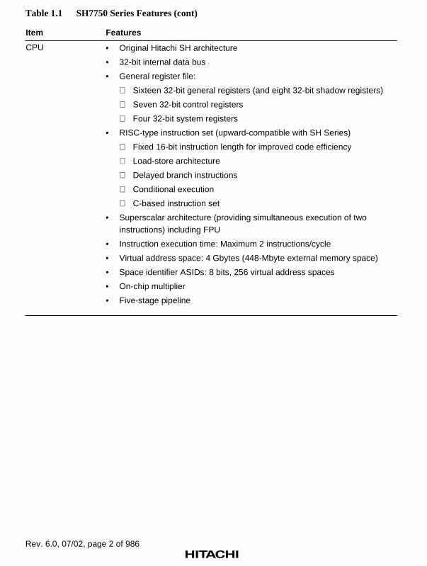
Rev. 6.0, 07/02, page 2 of 986
Table 1.1 SH7750 Series Features (cont)
Item Features
CPU • Original Hitachi SH architecture
• 32-bit internal data bus
• General register file:
Sixteen 32-bit general registers (and eight 32-bit shadow registers)
Seven 32-bit control registers
Four 32-bit system registers
• RISC-type instruction set (upward-compatible with SH Series)
Fixed 16-bit instruction length for improved code efficiency
Load-store architecture
Delayed branch instructions
Conditional execution
C-based instruction set
• Superscalar architecture (providing simultaneous execution of twoinstructions) including FPU
• Instruction execution time: Maximum 2 instructions/cycle
• Virtual address space: 4 Gbytes (448-Mbyte external memory space)
• Space identifier ASIDs: 8 bits, 256 virtual address spaces
• On-chip multiplier
• Five-stage pipeline

Rev. 6.0, 07/02, page 3 of 986
Table 1.1 SH7750 Series Features (cont)
Item Features
FPU • On-chip floating-point coprocessor
• Supports single-precision (32 bits) and double-precision (64 bits)
• Supports IEEE754-compliant data types and exceptions
• Two rounding modes: Round to Nearest and Round to Zero
• Handling of denormalized numbers: Truncation to zero or interruptgeneration for compliance with IEEE754
• Floating-point registers: 32 bits × 16 words × 2 banks(single-precision × 16 words or double-precision × 8 words) × 2 banks
• 32-bit CPU-FPU floating-point communication register (FPUL)
• Supports FMAC (multiply-and-accumulate) instruction
• Supports FDIV (divide) and FSQRT (square root) instructions
• Supports FLDI0/FLDI1 (load constant 0/1) instructions
• Instruction execution times
Latency (FMAC/FADD/FSUB/FMUL): 3 cycles (single-precision), 8cycles (double-precision)
Pitch (FMAC/FADD/FSUB/FMUL): 1 cycle (single-precision), 6 cycles(double-precision)
Note: FMAC is supported for single-precision only.
• 3-D graphics instructions (single-precision only):
4-dimensional vector conversion and matrix operations (FTRV): 4cycles (pitch), 7 cycles (latency)
4-dimensional vector inner product (FIPR): 1 cycle (pitch), 4 cycles(latency)

Rev. 6.0, 07/02, page 4 of 986
Table 1.1 SH7750 Series Features (cont)
Item Features
Clock pulsegenerator (CPG)
• Choice of main clock:
SH7750, SH7750S: 1/2, 1, 3, or 6 times EXTAL
SH7750R: 1, 6, or 12 times EXTAL
• Clock modes:
CPU frequency: 1, 1/2, 1/3, 1/4, 1/6, or 1/8 times main clock
Bus frequency: 1/2, 1/3, 1/4, 1/6, or 1/8 times main clock
Peripheral frequency: 1/2, 1/3, 1/4, 1/6, or 1/8 times main clock
Note: Maximum frequency varies with models.
• Power-down modes
Sleep mode
Standby mode
Module standby function
• Single-channel watchdog timer
Memorymanagementunit (MMU)
• 4-Gbyte address space, 256 address space identifiers (8-bit ASIDs)
• Single virtual mode and multiple virtual memory mode
• Supports multiple page sizes: 1 kbyte, 4 kbytes, 64 kbytes, 1 Mbyte
• 4-entry fully-associative TLB for instructions
• 64-entry fully-associative TLB for instructions and operands
• Supports software-controlled replacement and random-counterreplacement algorithm
• TLB contents can be accessed directly by address mapping

Rev. 6.0, 07/02, page 5 of 986
Table 1.1 SH7750 Series Features (cont)
Item Features
Cache memory[SH7750, SH7750S]
• Instruction cache (IC)
8 kbytes, direct mapping
256 entries, 32-byte block length
Normal mode (8-kbyte cache)
Index mode
• Operand cache (OC)
16 kbytes, direct mapping
512 entries, 32-byte block length
Normal mode (16-kbyte cache)
Index mode
RAM mode (8-kbyte cache + 8-kbyte RAM)
Choice of write method (copy-back or write-through)
• Single-stage copy-back buffer, single-stage write-through buffer
• Cache memory contents can be accessed directly by address mapping(usable as on-chip memory)
• Store queue (32 bytes × 2 entries)
Cache memory[SH7750R]
• Instruction cache (IC)
16 kbytes, 2-way set associative
256 entries/way, 32-byte block length
Cache-double-mode (16-kbyte cache)
Index mode
SH7750/SH7750S-compatible mode (8 kbytes, direct mapping)
• Operand cache (OC)
32 kbytes, 2-way set associative
512 entries/way, 32-byte block length
Cache-double-mode (32-kbyte cache)
Index mode
RAM mode (16-kbyte cache + 16-kbyte RAM)
SH7750/SH7750S-compatible mode (16 kbytes, direct mapping)
• Single-stage copy-back buffer, single-stage write-through buffer
• Cache memory contents can be accessed directly by address mapping(usable as on-chip memory)
• Store queue (32 bytes × 2 entries)

Rev. 6.0, 07/02, page 6 of 986
Table 1.1 SH7750 Series Features (cont)
Item Features
Interrupt controller(INTC)
• Five independent external interrupts: NMI, IRL3 to IRL0
• 15-level encoded external interrupts: IRL3 to IRL0
• On-chip peripheral module interrupts: Priority level can be set for eachmodule
User breakcontroller (UBC)
• Supports debugging by means of user break interrupts
• Two break channels
• Address, data value, access type, and data size can all be set as breakconditions
• Supports sequential break function
Bus statecontroller (BSC)
• Supports external memory access
64/32/16/8-bit external data bus
• External memory space divided into seven areas, each of up to 64Mbytes, with the following parameters settable for each area:
Bus size (8, 16, 32, or 64 bits)
Number of wait cycles (hardware wait function also supported)
Connection of DRAM, synchronous DRAM, and burst ROM possibleby setting space type
Supports fast page mode and DRAM EDO
Supports PCMCIA interface
Chip select signals (CS0 to CS6) output for relevant areas
• DRAM/synchronous DRAM refresh functions
Programmable refresh interval
Supports CAS-before-RAS refresh mode and self-refresh mode
• DRAM/synchronous DRAM burst access function
• Big endian or little endian mode can be set

Rev. 6.0, 07/02, page 7 of 986
Table 1.1 SH7750 Series Features (cont)
Item Features
Direct memoryaccess controller(DMAC)
• Physical address DMA controller:
SH7750, SH7750S: 4-channel
SH7750R: 8-channel
• Transfer data size: 8, 16, 32, or 64 bits, or 32 bytes
• Address modes:
Single address mode
Dual address mode
• Transfer requests: External, on-chip module, or auto-requests
• Bus modes: Cycle-steal or burst mode
• Supports on-demand data transfer
Timer unit (TMU) • Auto-reload 32-bit timer:
SH7750, SH7750S: 3-channel
SH7750R: 5-channel
• Input capture function
• Choice of seven counter input clocks
Realtime clock(RTC)
• On-chip clock and calendar functions
• Built-in 32 kHz crystal oscillator with maximum 1/256 second resolution(cycle interrupts)
Serialcommunicationinterface(SCI, SCIF)
• Two full-duplex communication channels (SCI, SCIF)
• Channel 1 (SCI):
Choice of asynchronous mode or synchronous mode
Supports smart card interface
• Channel 2 (SCIF):
Supports asynchronous mode
Separate 16-byte FIFOs provided for transmitter and receiver

Rev. 6.0, 07/02, page 8 of 986
Table 1.1 SH7750 Series Features (cont)
Item Features
Product lineup Abbre-viation
Voltage(Internal)
OperatingFrequency Model No. Package
SH7750 1.95 V 200 MHz HD6417750BP200M 256-pin BGA
1.8 V 167 MHz HD6417750F167HD6417750F167I
1.5 V 128 MHz HD6417750VF128
208-pin QFP
SH7750S 1.95 V 200 MHz HD6417750SBP200 256-pin BGA
HD6417750SF200
1.8 V 167 MHz HD6417750SF167HD6417750SF167I
1.5 V 133 MHz HD6417750SVF133
208-pin QFP
HD6417750SVBT133 264-pin CSP
SH7750R 1.5 V 240 MHz HD6417750RBP240 256-pin BGA
HD6417750RF240 208-pin QFP
200 MHz HD6417750RBP200 256-pin BGA
HD6417750RF200 208-pin QFP
Notes: *1 For SH7750R only*2 For SH7750S only
*3 For SH7750 only

Rev. 6.0, 07/02, page 9 of 986
1.2 Block Diagram
Figure 1.1 shows an internal block diagram of the SH7750 Series.
CPG
INTC
SCI(SCIF)
RTC
TMU
Externalbus interface
BSC DMAC
Add
ress
29-b
it ad
dres
s
64-b
it da
ta
64-b
it da
ta
32-b
it da
ta
32-b
it da
ta
Upp
er 3
2-bi
t dat
a
32-b
it ad
dres
s (in
stru
ctio
ns)
32-b
it da
ta (
inst
ruct
ions
)
32-b
it ad
dres
s (d
ata)
Per
iphe
ral a
ddre
ss b
us
26-bitaddress 64-bit
data
16-b
it pe
riphe
ral d
ata
bus
UBC
Lower 32-bit data
Lower 32-bit data
32-b
it da
ta (
load
)
32-b
it da
ta (
stor
e)
CPU
I cache O cacheITLB UTLBCache and
TLB controller
FPU
64-b
it da
ta (
stor
e)
BSC: Bus state controllerCPG: Clock pulse generatorDMAC: Direct memory access controllerFPU: Floating-point unitINTC: Interrupt controllerITLB: Instruction TLB (translation lookaside buffer)
UTLB: Unified TLB (translation lookaside buffer)RTC: Realtime clockSCI: Serial communication interfaceSCIF: Serial communication interface with FIFOTMU: Timer unitUBC: User break controller
Figure 1.1 Block Diagram of SH7750 Series Functions

Rev. 6.0, 07/02, page 10 of 986
1.3 Pin Arrangement
NMI
MD1/TXD2MD0/SCK
D50
D51
D52
D53
D63
D62
D61
D57
D56
D31
D30
D29
D28
D27
D26
D25
D54
D55
D16
D17
D18
D19
D20
D21
D48
D49
D60
D59
D58
EX
TA
L
XT
AL
VS
S-C
PG
VD
D-C
PG
(3.3
V)
VD
D-P
LL1(
3.3V
)V
DD
-PLL
2(3.
3V)
TD
IT
CK
TM
ST
DO
/BR
KA
CK
MD
6/S
TA
TU
S1
ST
AT
US
0D
AC
K1
DA
CK
0M
D5/
MD
4/
MD
3/A
25A
24A
23A
22A
21A
20A
19A
18M
D7/
TX
DS
CK
2/M
D8/
TC
LK
VD
D-R
TC
(3.3
V)
VS
S-R
TC
EX
TA
L2X
TA
L2
D8
D7
CK
E/
/DQ
M5
//D
QM
4/
/DQ
M1
//D
QM
0A
17A
16A
15A
14A
13A
12A
11A
10 A9
A8
A7
CK
IOC
KIO
2A
6A
5A
4A
3A
2
// R
D/
//D
QM
2//
/DQ
M3/
//D
QM
6/
/DQ
M7/
D23
D24
D22
A
B
C
D
E
F
G
H
1 2 3 4 5 6 7 8 9 10 11 12 13 14 15 16 17 19 2018
J
K
L
M
N
P
R
T
U
V
W
Y
D47
D46
D45
D44
D43
D42
D32
D33
D34
D35
D36
D37
DR
AK
0D
RA
K1
VS
S-P
LL1
VS
S-P
LL2
A1
A0
RD/
BGA256(Top view)
MD2/RXD2
RXD
/
D41
D40
D15
D14
D13
D12
D11
D10
D9
D38
D39
D0
D1
D2
D3
D4
D5
D6
/
VDDQ (IO)
VSSQ (IO)
VDD (internal)
VSS (internal)
NC
CA*
Note: Power must be supplied to the on-chip PLL power supply pins (VDD-PLL1, VDD-PLL2, VSS-PLL1, VSS-PLL2, VDD-CPG, VSS-CPG, VDD-RTC, and VSS-RTC) regardless of whether or not the PLL circuits, crystal resonator, and RTC are used.* Hardware standby request (SH7750S and SH7750R). In the SH7750, pull up to 3.3 V.
Figure 1.2 Pin Arrangement (256-Pin BGA)

Rev. 6.0, 07/02, page 11 of 986
12345678910111213141516171819202122232425262728293031323334353637383940414243444546474849505152
D47D32
D46D33D45D34D44D35
D43D36D42D37D41D38D40D39
D15D0
D14D1
D13D2
D12D3
D11D4
D10D5D9D6
//
156155154153152151150149148147146145144143142141140139138137136135134133132131130129128127126125124123122121120119118117116115114113112111110109108107106105
NMI
MD2/RXD2MD1/TXD2MD0/SCK
D63D48
D62D49D61D50D60D51
D59D52D58D53D57D54D56D55
D31D16D30D17D29D18
D28D19
D27D20D26D21D25
RXD
53 54 55 56 57 58 59 60 61 62 63 64 65 66 67 68 69 70 71 72 73 74 75 76 77 78 79 80 81 82 83 84 85 86 87 88 89 90 91 92 93 94 95 96 97 98 99 100
101
102
103
104
D8
D7
CK
E
//D
QM
5/
/DQ
M4
//D
QM
1/
/DQ
M0
A17
A16
A15
A14
A13
A12
A11
A10 A
9A
8A
7C
KIO A6
A5
A4
A3
A2
DR
AK
1D
RA
K0
// R
D/
//D
QM
2//
/DQ
M3/
//D
QM
6
//D
QM
7/D
23D
24D
22
208
207
206
205
204
203
202
201
200
199
198
197
196
195
194
193
192
191
190
189
188
187
186
185
184
183
182
181
180
179
178
177
176
175
174
173
172
171
170
169
168
167
166
165
164
163
162
161
160
159
158
157
EX
TA
LX
TA
LV
SS
-CP
GV
DD
-CP
G(3
.3V
)V
SS
-PLL
1V
DD
-PLL
1(3.
3V)
VS
S-P
LL2
VD
D-P
LL2(
3.3V
)
TD
IT
CK
TM
S
TD
O/B
RK
AC
KM
D6/
ST
AT
US
1S
TA
TU
S0
A1
A0
DA
CK
1D
AC
K0
MD
5/M
D4/
MD
3/A
25A
24
A23
A22
A21
A20
A19
A18
SC
K2/
MD
7/T
XD
MD
8/T
CLK
CA
*V
DD
-RT
C(3
.3V
)V
SS
-RT
CE
XT
AL2
XT
AL2
QFP208
Top view
VDD (internal)
VSS (internal)
VDDQ (IO)
VSSQ (IO)
Note: Power must be supplied to the on-chip PLL power supply pins (VDD-PLL1, VDD-PLL2, VSS-PLL1, VSS-PLL2, VDD-CPG, VSS-CPG, VDD-RTC, and VSS-RTC) regardless of whether or not the PLL circuits, crystal resonator, and RTC are used.* Hardware standby request (SH7750S and SH7750R). In the SH7750, pull up to 3.3 V.
Figure 1.3 Pin Arrangement (208-Pin QFP)

Rev. 6.0, 07/02, page 12 of 986
VDDQ (IO)
VSSQ (IO)
VDD (internal)
VSS (internal)
NC
A
B
C
D
E
F
G
H
1
VSS-CPG XTAL EXTAL VDD-CPG TDO MD6 A0 VDDQ VDDQ A20 VDD TCLK VSS-RTC XTAL2 EXTAL2
VDD-PLL2 VSS STATUS0 DACK0 A24 VDDQ MD7/TXD CA
VSS-PLL2 VSS-PLL1 VDD-PLL1 TCK VSSQ VSSQ MD3/ A22 A18 VDDQ VDDQ VDD-RTC MD1/TXD2 NMI
VSSQ TDI VDD A1 MD5/ A23 VSS MD8/ VSSQ
TMS VDDQ VDDQ MD4/ VSSQ VSSQ SCK2 D48 RD/ MD2/RXD2 VSSQ
VDD D47 VDDQ D32 D33 STATUS1 DACK1 VSSQ A25 A21 A19 D49 VDDQ D63 MD0/SCK D62
D45 VDDQ D46 VSS VSSQ D34 D50 VDDQ VDD VSSQ VSS D61
VDDQ D43 D44 D35 VSSQ D36 D52 VDDQ D51 VSSQ D60 D59
VDDQ D38 D42 D41 D37 VSSQ VSSQ D57 D53 D54 D58 VDDQ
D39 D0 VSSQ D15 VDDQ D40 D56 VSSQ D31 D16 D55 VDDQ
D1 VSS VSSQ VDD VDDQ D14 D30 VSSQ VSS D18 VDDQ D17
D2 D4 D3 VDDQ D13 D14 A9 VDDQ A6 A2 D29 D28 D27 VDDQ D19 VDD
VSSQ D5 D11 D12 A16 VDDQ VDDQ A7 A4 DRAK0 VSSQ VSS D26 D21 VDDQ D20
VSSQ VDDQ VDDQ VDD A11 VSSQ VSSQ VSSQ VSSQ D25
D6 D10 CKE A17 VSS A12 A8 VDDQ VDDQ RXD
VSSQ D8 VDDQ VSSQ A13 VSSQ CKIO2 A3 VDD RD/ D24 D22 VSSQ
D9 D7 A15 VSSQ A10 CKIO A5 DRAK1 VDDQ VDDQ D23 VSSQ
2 3 4 5 6 7 8 9 10 11 12 13 14 15 16 17
J
K
L
M
N
P
R
T
U
CSP264
(Top view)
Note: Power must be supplied to the on-chip PLL power supply pins (VDD-PLL1, VDD-PLL2, VSS-PLL1, VSS-PLL2, VDD-CPG, VSS-CPG, VDD-RTC, and VSS-RTC) regardless of whether or not the PLL circuits, crystal resonator, and RTC are used.
Figure 1.4 Pin Arrangement (264-Pin CSP)

Rev. 6.0, 07/02, page 13 of 986
1.4 Pin Functions
1.4.1 Pin Functions (256-Pin BGA)
Table 1.2 Pin Functions
Memory Interface
No.PinNo. Pin Name I/O Function Reset SRAM DRAM SDRAM PCMCIA MPX
1 B2 RDY I Bus ready RDY RDY RDY
2 B1 RESET I Reset RESET
3 C2 CS0 O Chip select 0 CS0 CS0
4 C1 CS1 O Chip select 1 CS1 CS1
5 D4 CS4 O Chip select 4 CS4 CS4
6 D3 CS5 O Chip select 5 CS5 CE1A CS5
7 D2 CS6 O Chip select 6 CS6 CE1B CS6
8 D1 BS O Bust start (BS) (BS) (BS) (BS) (BS)
9 E4 VSSQ Power IO GND (0 V)
10 E3 RD2 O RD/CASS/FRAME
OE CAS OE FRAME
11 F3 VDDQ Power IO VDD (3.3 V)
12 F4 VSSQ Power IO GND (0 V)
13 E2 D47 I/O Data/port (Port) (Port) (Port) (Port) (Port)
14 E1 D32 I/O Data/port (Port) (Port) (Port) (Port) (Port)
15 G3 VDD Power Internal VDD(1.8 V)
16 G4 VSS Power Internal GND(0 V)
17 F2 D46 I/O Data/port (Port) (Port) (Port) (Port) (Port)
18 F1 D33 I/O Data/port (Port) (Port) (Port) (Port) (Port)
19 H3 VDDQ Power IO VDD (3.3 V)
20 H4 VSSQ Power IO GND (0 V)
21 G2 D45 I/O Data/port (Port) (Port) (Port) (Port) (Port)
22 G1 D34 I/O Data/port (Port) (Port) (Port) (Port) (Port)
23 H2 D44 I/O Data/port (Port) (Port) (Port) (Port) (Port)
24 H1 D35 I/O Data/port (Port) (Port) (Port) (Port) (Port)
25 J3 VDDQ Power IO VDD (3.3 V)
26 J4 VSSQ Power IO GND (0 V)
27 J2 D43 I/O Data/port (Port) (Port) (Port) (Port) (Port)
28 J1 D36 I/O Data/port (Port) (Port) (Port) (Port) (Port)

Rev. 6.0, 07/02, page 14 of 986
Table 1.2 Pin Functions (cont)
Memory Interface
No.PinNo. Pin Name I/O Function Reset SRAM DRAM SDRAM PCMCIA MPX
29 K2 D42 I/O Data/port (Port) (Port) (Port) (Port) (Port)
30 K1 D37 I/O Data/port (Port) (Port) (Port) (Port) (Port)
31 K3 VDDQ Power IO VDD (3.3 V)
32 K4 VSSQ Power IO GND (0 V)
33 L1 D41 I/O Data/port (Port) (Port) (Port) (Port) (Port)
34 L2 D38 I/O Data/port (Port) (Port) (Port) (Port) (Port)
35 M1 D40 I/O Data/port (Port) (Port) (Port) (Port) (Port)
36 M2 D39 I/O Data/port (Port) (Port) (Port) (Port) (Port)
37 L3 VDDQ Power IO VDD (3.3 V)
38 L4 VSSQ Power IO GND (0 V)
39 N1 D15 I/O Data A15
40 N2 D0 I/O Data A0
41 P1 D14 I/O Data A14
42 P2 D1 I/O Data A1
43 M3 VDDQ Power IO VDD (3.3 V)
44 M4 VSSQ Power IO GND (0 V)
45 R1 D13 I/O Data A13
46 R2 D2 I/O Data A2
47 P3 VDD Power Internal VDD
48 P4 VSS Power Internal GND(0 V)
49 T1 D12 I/O Data A12
50 T2 D3 I/O Data A3
51 R3 VDDQ Power IO VDD (3.3 V)
52 R4 VSSQ Power IO GND (0 V)
53 U1 D11 I/O Data A11
54 U2 D4 I/O Data A4
55 V1 D10 I/O Data A10
56 V2 D5 I/O Data A5
57 T3 VDDQ Power IO VDD (3.3 V)
58 T4 VSSQ Power IO GND (0 V)
59 W1 D9 I/O Data A9
60 Y1 D6 I/O Data A6

Rev. 6.0, 07/02, page 15 of 986
Table 1.2 Pin Functions (cont)
Memory Interface
No.PinNo. Pin Name I/O Function Reset SRAM DRAM SDRAM PCMCIA MPX
61 U3 BACK/BSREQ
O Busacknowledge/bus request
62 V3 BREQ/BSACK
I Busrequest/busacknowledge
63 W2 D8 I/O Data A8
64 Y2 D7 I/O Data A7
65 W3 CKE O Clock outputenable
CKE
66 V5 VDDQ Power IO VDD (3.3 V)
67 U5 VSSQ Power IO GND (0 V)
68 Y3 WE5/CAS5/DQM5
O D47–D40select signal
WE5 CAS5 DQM5
69 W4 WE4/CAS4/DQM4
O D39–D32select signal
WE4 CAS4 DQM4
70 Y4 WE1/CAS1/DQM1
O D15–D8 selectsignal
WE1 CAS1 DQM1 WE1
71 W5 WE0/CAS0/DQM0
O D7–D0 selectsignal
WE0 CAS0 DQM0
72 Y5 A17 O Address
73 V6 VDDQ Power IO VDD (3.3 V)
74 U6 VSSQ Power IO GND (0 V)
75 W6 A16 O Address
76 Y6 A15 O Address
77 V7 VDD Power Internal VDD
78 U7 VSS Power Internal GND(0 V)
79 W7 A14 O Address
80 Y7 A13 O Address
81 V8 VDDQ Power IO VDD (3.3 V)
82 U8 VSSQ Power IO GND (0 V)
83 V4 NC
84 W8 A12 O Address
85 Y8 A11 O Address
86 W9 A10 O Address

Rev. 6.0, 07/02, page 16 of 986
Table 1.2 Pin Functions (cont)
Memory Interface
No.PinNo. Pin Name I/O Function Reset SRAM DRAM SDRAM PCMCIA MPX
87 V9 VDDQ Power IO VDD (3.3 V)
88 U9 VSSQ Power IO GND (0 V)
89 Y9 A9 O Address
90 W10 A8 O Address
91 Y10 A7 O Address
92 Y11 CKIO O Clock output CKIO
93 V10 VDDQ Power IO VDD (3.3 V)
94 U10 VSSQ Power IO GND (0 V)
95 W11 CKIO2 O CKIO*1 CKIO
96 Y12 A6 O Address
97 W12 A5 O Address
98 Y13 A4 O Address
99 V11 VDDQ Power IO VDD (3.3 V)
100 U11 VSSQ Power IO GND (0 V)
101 W13 A3 O Address
102 Y14 A2 O Address
103 V12 DRAK1 O DMAC1requestacknowledge
104 U13 DRAK0 O DMAC0requestacknowledge
105 V13 VDDQ Power IO VDD (3.3 V)
106 U12 VSSQ Power IO GND (0 V)
107 W14 CS3 O Chip select 3 CS3 (CS3) CS3 CS3
108 Y15 CS2 O Chip select 2 CS2 (CS2) CS2 CS2
109 V14 VDD Power Internal VDD
110 U14 VSS Power Internal GND(0 V)
111 W15 RAS O RAS RAS RAS
112 Y16 RD/CASS/FRAME
O Read/CAS/FRAME
OE CAS OE FRAME
113 V15 VDDQ Power IO VDD (3.3 V)
114 U15 VSSQ Power IO GND (0 V)

Rev. 6.0, 07/02, page 17 of 986
Table 1.2 Pin Functions (cont)
Memory Interface
No.PinNo. Pin Name I/O Function Reset SRAM DRAM SDRAM PCMCIA MPX
115 W16 RD/WR O Read/write RD/WR RD/WR RD/WR RD/WR
116 Y17 WE2/CAS2/DQM2/ICIORD
O D23–D16select signal
WE2 CAS2 DQM2 ICIORD
117 W17 WE3/CAS3/DQM3/ICIOWR
O D31–D24select signal
WE3 CAS3 DQM3 ICIOWR
118 Y18 WE6/CAS6/DQM6
O D55–D48select signal
WE6 CAS6 DQM6
119 V16 VDDQ Power IO VDD (3.3 V)
120 U16 VSSQ Power IO GND (0 V)
121 W18 WE7/CAS7/DQM7/REG
O D63–D56select signal
WE7 CAS7 DQM7 REG
122 Y19 D23 I/O Data A23
123 W19 D24 I/O Data A24
124 Y20 D22 I/O Data A22
125 V17 RXD I SCI data input
126 U17 DREQ0 I Request fromDMAC0
127 U18 DREQ1 I Request fromDMAC1
128 W20 D25 I/O Data A25
129 T18 VDDQ Power IO VDD (3.3 V)
130 T17 VSSQ Power IO GND (0 V)
131 V19 D21 I/O Data A21
132 V20 D26 I/O Data
133 U19 D20 I/O Data A20
134 U20 D27 I/O Data
135 R18 VDDQ Power IO VDD (3.3 V)
136 R17 VSSQ Power IO GND (0 V)
137 T19 D19 I/O Data A19
138 T20 D28 I/O Data
139 P18 VDD Power Internal VDD
140 P17 VSS Power Internal GND(0 V)
141 R19 D18 I/O Data A18

Rev. 6.0, 07/02, page 18 of 986
Table 1.2 Pin Functions (cont)
Memory Interface
No.PinNo. Pin Name I/O Function Reset SRAM DRAM SDRAM PCMCIA MPX
142 R20 D29 I/O Data
143 N18 VDDQ Power IO VDD (3.3 V)
144 N17 VSSQ Power IO GND (0 V)
145 P19 D17 I/O Data A17
146 P20 D30 I/O Data
147 N19 D16 I/O Data A16
148 N20 D31 I/O Data
149 M18 VDDQ Power IO VDD (3.3 V)
150 M17 VSSQ Power IO GND (0 V)
151 M19 D55 I/O Data
152 M20 D56 I/O Data
153 L19 D54 I/O Data
154 L20 D57 I/O Data
155 L18 VDDQ Power IO VDD (3.3 V)
156 L17 VSSQ Power IO GND (0 V)
157 K20 D53 I/O Data
158 K19 D58 I/O Data
159 J20 D52 I/O Data
160 J19 D59 I/O Data
161 K18 VDDQ Power IO VDD (3.3 V)
162 K17 VSSQ Power IO GND (0 V)
163 H20 D51 I/O Data/port (Port) (Port) (Port) (Port) (Port)
164 H19 D60 I/O Data
165 G20 D50 I/O Data/port (Port) (Port) (Port) (Port) (Port)
166 G19 D61 I/O Data ACCSIZE0
167 J18 VDDQ Power IO VDD (3.3 V)
168 J17 VSSQ Power IO GND (0 V)
169 F20 D49 I/O Data/port (Port) (Port) (Port) (Port) (Port)
170 F19 D62 I/O Data ACCSIZE1
171 G18 VDD Power Internal VDD
172 G17 VSS Power Internal GND(0 V)
173 E20 D48 I/O Data/port (Port) (Port) (Port) (Port) (Port)
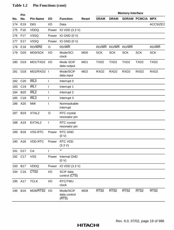
Rev. 6.0, 07/02, page 19 of 986
Table 1.2 Pin Functions (cont)
Memory Interface
No.PinNo. Pin Name I/O Function Reset SRAM DRAM SDRAM PCMCIA MPX
174 E19 D63 I/O Data ACCSIZE2
175 F18 VDDQ Power IO VDD (3.3 V)
176 F17 VSSQ Power IO GND (0 V)
177 E17 VSSQ Power IO GND (0 V)
178 E18 RD/WR2 O RD/WR RD/WR RD/WR RD/WR RD/WR
179 D20 MD0/SCK I/O Mode/SCIclock
MD0 SCK SCK SCK SCK SCK
180 D19 MD1/TXD2 I/O Mode SCIFdata output
MD1 TXD2 TXD2 TXD2 TXD2 TXD2
181 D18 MD2/RXD2 I Mode/SCIFdata input
MD2 RXD2 RXD2 RXD2 RXD2 RXD2
182 C20 IRL0 I Interrupt 0
183 C19 IRL1 I Interrupt 1
184 B20 IRL2 I Interrupt 2
185 C18 IRL3 I Interrupt 3
186 A20 NMI I Nonmaskableinterrupt
187 B19 XTAL2 O RTC crystalresonator pin
188 A19 EXTAL2 I RTC crystalresonator pin
189 B18 VSS-RTC Power RTC GND(0 V)
190 A18 VDD-RTC Power RTC VDD(3.3 V)
191 D17 CA I *2
192 C17 VSS Power Internal GND(0 V)
193 B17 VDDQ Power IO VDD (3.3 V)
194 C16 CTS2 I/O SCIF datacontrol (CTS)
195 A17 TCLK I/O RTC/TMUclock
196 B16 MD8/RTS2 I/O Mode/SCIFdata control(RTS)
MD8 RTS2 RTS2 RTS2 RTS2 RTS2

Rev. 6.0, 07/02, page 20 of 986
Table 1.2 Pin Functions (cont)
Memory Interface
No.PinNo. Pin Name I/O Function Reset SRAM DRAM SDRAM PCMCIA MPX
197 C15 VDDQ Power IO VDD (3.3 V)
198 D15 VSSQ Power IO GND (0 V)
199 B15 MD7/TXD I/O Mode/SCIdata output
MD7 TXD TXD TXD TXD TXD
200 A16 SCK2/MRESET
I SCIF clock/manual reset
MRESET SCK2 SCK2 SCK2 SCK2 SCK2
201 C14 VDD Power Internal VDD
202 D14 VSS Power Internal GND(0 V)
203 A15 A18 O Address
204 B14 A19 O Address
205 C13 VDDQ Power IO VDD (3.3 V)
206 D13 VSSQ Power IO GND (0 V)
207 A14 A20 O Address
208 B13 A21 O Address
209 A13 A22 O Address
210 B12 A23 O Address
211 C12 VDDQ Power IO VDD (3.3 V)
212 D12 VSSQ Power IO GND (0 V)
213 A12 A24 O Address
214 B11 A25 O Address
215 A11 MD3/CE2A I/O Mode/PCMCIA-CE
MD3 CE2A
216 A10 MD4/CE2B I/O Mode/PCMCIA-CE
MD4 CE2B
217 C11 VDDQ Power IO VDD (3.3 V)
218 D11 VSSQ Power IO GND (0 V)
219 B10 MD5/RAS2 I/O Mode/RAS(DRAM)
MD5 RAS2
220 A9 DACK0 O DMAC0 busacknowledge
221 B9 DACK1 O DMAC1 busacknowledge
222 C8 A0 O Address
223 C10 VDDQ Power IO VDD (3.3 V)
224 D10 VSSQ Power IO GND (0 V)

Rev. 6.0, 07/02, page 21 of 986
Table 1.2 Pin Functions (cont)
Memory Interface
No.PinNo. Pin Name I/O Function Reset SRAM DRAM SDRAM PCMCIA MPX
225 D8 A1 O Address
226 A8 STATUS0 O Status
227 B8 STATUS1 O Status
228 A7 MD6/IOIS16
I Mode/IOIS16(PCMCIA)
MD6 IOIS16
229 C9 VDDQ Power IO VDD (3.3 V)
230 D9 VSSQ Power IO GND (0 V)
231 B7 ASEBRK/BRKACK
I/O Pin break/acknowledge(H-UDI)
232 A6 TDO O Data out(H-UDI)
233 C7 VDD Power Internal VDD
234 D7 VSS Power Internal GND(0 V)
235 B6 TMS I Mode(H-UDI)
236 A5 TCK I Clock(H-UDI)
237 B5 TDI I Data in(H-UDI)
238 C4 TRST I Reset(H-UDI)
239 C3 CKIO2ENB I CKIO2, RD2,RD/WR2enable
240 C6 NC
241 A4 VDD-PLL2 Power PLL2 VDD(3.3V)
242 D6 VSS-PLL2 Power PLL2 GND (0V)
243 B4 VDD-PLL1 Power PLL1 VDD(3.3V)
244 D5 VSS-PLL1 Power PLL1 GND (0V)
245 A3 VDD-CPG Power CPG VDD(3.3V)
246 B3 VSS-CPG Power CPG GND (0V)
247 A2 XTAL O Crystalresonator

Rev. 6.0, 07/02, page 22 of 986
Table 1.2 Pin Functions (cont)
Memory Interface
No.PinNo. Pin Name I/O Function Reset SRAM DRAM SDRAM PCMCIA MPX
248 A1 EXTAL I External inputclock/crystalresonator
249 C5 NC
250 D16 NC
251 H17 NC
252 H18 NC
253 N3 NC
254 N4 NC
255 U4 NC
256 V18 NC
I: InputO: Output
I/O: Input/outputPower: Power supply
Notes: 1. Except in hardware standby mode, supply power to all power pins. In hardware standbymode, supply power to RTC as a minimum.
2. Power must be supplied to VDD-PLL1/2 and VSS-PLL1/2 regardless of whether or notthe on-chip PLL circuits are used.
3. Power must be supplied to VDD-CPG and VSS-CPG regardless of whether or not theon-chip crystal resonator is used.
4. Power must be supplied to VDD-RTC and VSS-RTC regardless of whether or not theon-chip RTC is used.
5. VSSQ, VSS, VSS-RTC, VSS-PLL1/2, and VSS-CPG are connected inside the package.6. In the SH7750S and SH7750R, at least the RTC power supply must be supplied in
hardware standby mode.
7. NC pins must be left completely open, and not connected to a power supply, GND, etc.*1 CKIO2 is not connected to PLL2.*2 Hardware standby request (SH7750S and SH7750R). In the SH7750, pull up to 3.3 V.

Rev. 6.0, 07/02, page 23 of 986
1.4.2 Pin Functions (208-Pin QFP)
Table 1.3 Pin Functions
Memory InterfacePinNo. Pin Name I/O Function Reset SRAM DRAM SDRAM PCMCIA MPX
1 RDY I Bus ready RDY RDY RDY
2 RESET I Reset RESET
3 CS0 O Chip select 0 CS0 CS0
4 CS1 O Chip select 1 CS1 CS1
5 CS4 O Chip select 4 CS4 CS4
6 CS5 O Chip select 5 CS5 CE1A CS5
7 CS6 O Chip select 6 CS6 CE1B CS6
8 BS O Bust start (BS) (BS) (BS) (BS) (BS)
9 VDDQ Power IO VDD (3.3 V)
10 VSSQ Power IO GND (0 V)
11 D47 I/O Data/port (Port) (Port) (Port) (Port) (Port)
12 D32 I/O Data/port (Port) (Port) (Port) (Port) (Port)
13 VDD Power Internal VDD
14 VSS Power Internal GND(0 V)
15 D46 I/O Data/port (Port) (Port) (Port) (Port) (Port)
16 D33 I/O Data/port (Port) (Port) (Port) (Port) (Port)
17 D45 I/O Data/port (Port) (Port) (Port) (Port) (Port)
18 D34 I/O Data/port (Port) (Port) (Port) (Port) (Port)
19 D44 I/O Data/port (Port) (Port) (Port) (Port) (Port)
20 D35 I/O Data/port (Port) (Port) (Port) (Port) (Port)
21 VDDQ Power IO VDD (3.3 V)
22 VSSQ Power IO GND (0 V)
23 D43 I/O Data/port (Port) (Port) (Port) (Port) (Port)
24 D36 I/O Data/port (Port) (Port) (Port) (Port) (Port)
25 D42 I/O Data/port (Port) (Port) (Port) (Port) (Port)
26 D37 I/O Data/port (Port) (Port) (Port) (Port) (Port)
27 D41 I/O Data/port (Port) (Port) (Port) (Port) (Port)
28 D38 I/O Data/port (Port) (Port) (Port) (Port) (Port)
29 D40 I/O Data/port (Port) (Port) (Port) (Port) (Port)
30 D39 I/O Data/port (Port) (Port) (Port) (Port) (Port)

Rev. 6.0, 07/02, page 24 of 986
Table 1.3 Pin Functions (cont)
Memory InterfacePinNo. Pin Name I/O Function Reset SRAM DRAM SDRAM PCMCIA MPX
31 VDDQ Power IO VDD (3.3 V)
32 VSSQ Power IO GND (0 V)
33 D15 I/O Data A15
34 D0 I/O Data A0
35 D14 I/O Data A14
36 D1 I/O Data A1
37 D13 I/O Data A13
38 D2 I/O Data A2
39 VDD Power Internal VDD(1.8 V)
40 VSS Power Internal GND(0 V)
41 D12 I/O Data A12
42 D3 I/O Data A3
43 VDDQ Power IO VDD (3.3 V)
44 VSSQ Power IO GND (0 V)
45 D11 I/O Data A11
46 D4 I/O Data A4
47 D10 I/O Data A10
48 D5 I/O Data A5
49 D9 I/O Data A9
50 D6 I/O Data A6
51 BACK/BSREQ
O Busacknowledge/bus request
52 BREQ/BSACK
I Bus request/busacknowledge
53 D8 I/O Data A8
54 D7 I/O Data A7
55 CKE O Clock outputenable
CKE
56 VDDQ Power IO VDD (3.3 V)
57 VSSQ Power IO GND (0 V)
58 WE5/CAS5/DQM5
O D47–D40 selectsignal
WE5 CAS5 DQM5

Rev. 6.0, 07/02, page 25 of 986
Table 1.3 Pin Functions (cont)
Memory InterfacePinNo. Pin Name I/O Function Reset SRAM DRAM SDRAM PCMCIA MPX
59 WE4/CAS4/DQM4
O D39–D32 selectsignal
WE4 CAS4 DQM4
60 WE1/CAS1/DQM1
O D15–D8 selectsignal
WE1 CAS1 DQM1 WE1
61 WE0/CAS0/DQM0
O D7–D0 selectsignal
WE0 CAS0 DQM0
62 A17 O Address
63 A16 O Address
64 A15 O Address
65 VDD Power Internal VDD
66 VSS Power Internal GND(0 V)
67 A14 O Address
68 A13 O Address
69 VDDQ Power IO VDD (3.3 V)
70 VSSQ Power IO GND (0 V)
71 A12 O Address
72 A11 O Address
73 A10 O Address
74 A9 O Address
75 A8 O Address
76 A7 O Address
77 CKIO O Clock output CKIO
78 VDDQ Power IO VDD (3.3 V)
79 VSSQ Power IO GND (0 V)
80 A6 O Address
81 A5 O Address
82 A4 O Address
83 A3 O Address
84 A2 O Address
85 DRAK1 O DMAC1 requestacknowledge
86 DRAK0 O DMAC0 requestacknowledge
87 VDDQ Power IO VDD (3.3 V)

Rev. 6.0, 07/02, page 26 of 986
Table 1.3 Pin Functions (cont)
Memory InterfacePinNo. Pin Name I/O Function Reset SRAM DRAM SDRAM PCMCIA MPX
88 VSSQ Power IO GND (0 V)
89 CS3 O Chip select 3 CS3 (CS3) CS3 CS3
90 CS2 O Chip select 2 CS2 (CS2) CS2 CS2
91 VDD Power Internal VDD
92 VSS Power Internal GND(0 V)
93 RAS O RAS RAS RAS
94 RD/CASS/FRAME
O Read/CAS/FRAME
OE CAS OE FRAME
95 RD/WR O Read/write RD/WR RD/WR RD/WR RD/WR
96 WE2/CAS2/DQM2/ICIORD
O D23–D16 selectsignal
WE2 CAS2 DQM2 ICIORD
97 WE3/CAS3/DQM3/ICIOWR
O D31–D24 selectsignal
WE3 CAS3 DQM3 ICIOWR
98 WE6/CAS6/DQM6
O D55–D48 selectsignal
WE6 CAS6 DQM6
99 VDDQ Power IO VDD (3.3 V)
100 VSSQ Power IO GND (0 V)
101 WE7/CAS7/DQM7/REG
O D63–D56 selectsignal
WE7 CAS7 DQM7 REG
102 D23 I/O Data A23
103 D24 I/O Data A24
104 D22 I/O Data A22
105 RXD I SCI Data input
106 DREQ0 I Request fromDMAC0
107 DREQ1 I Request fromDMAC1
108 D25 I/O Data A25
109 D21 I/O Data A21
110 D26 I/O Data
111 D20 I/O Data A20
112 D27 I/O Data
113 VDDQ Power IO VDD (3.3 V)

Rev. 6.0, 07/02, page 27 of 986
Table 1.3 Pin Functions (cont)
Memory InterfacePinNo. Pin Name I/O Function Reset SRAM DRAM SDRAM PCMCIA MPX
114 VSSQ Power IO GND (0 V)
115 D19 I/O Data A19
116 D28 I/O Data
117 VDD Power Internal VDD
118 VSS Power Internal GND(0 V)
119 D18 I/O Data A18
120 D29 I/O Data
121 D17 I/O Data A17
122 D30 I/O Data
123 D16 I/O Data A16
124 D31 I/O Data
125 VDDQ Power IO VDD (3.3 V)
126 VSSQ Power IO GND (0 V)
127 D55 I/O Data
128 D56 I/O Data
129 D54 I/O Data
130 D57 I/O Data
131 D53 I/O Data
132 D58 I/O Data
133 D52 I/O Data
134 D59 I/O Data
135 VDDQ Power IO VDD (3.3 V)
136 VSSQ Power IO GND (0 V)
137 D51 I/O Data/port (Port) (Port) (Port) (Port) (Port)
138 D60 I/O Data
139 D50 I/O Data/port (Port) (Port) (Port) (Port) (Port)
140 D61 I/O Data ACCSIZE0
141 D49 I/O Data/port (Port) (Port) (Port) (Port) (Port)
142 D62 I/O Data ACCSIZE1
143 VDD Power Internal VDD
144 VSS Power Internal GND(0 V)

Rev. 6.0, 07/02, page 28 of 986
Table 1.3 Pin Functions (cont)
Memory InterfacePinNo. Pin Name I/O Function Reset SRAM DRAM SDRAM PCMCIA MPX
145 D48 I/O Data/port (Port) (Port) (Port) (Port) (Port)
146 D63 I/O Data ACCSIZE2
147 VDDQ Power IO VDD (3.3 V)
148 VSSQ Power IO GND (0 V)
149 MD0/SCK I/O Mode/SCI clock MD0 SCK SCK SCK SCK SCK
150 MD1/TXD2 I/O Mode SCIF dataoutput
MD1 TXD2 TXD2 TXD2 TXD2 TXD2
151 MD2/RXD2 I Mode/SCIF datainput
MD2 RXD2 RXD2 RXD2 RXD2 RXD2
152 IRL0 I Interrupt 0
153 IRL1 I Interrupt 1
154 IRL2 I Interrupt 2
155 IRL3 I Interrupt 3
156 NMI I Nonmaskableinterrupt
157 XTAL2 O RTC crystalresonator pin
158 EXTAL2 I RTC crystalresonator pin
159 VSS-RTC Power RTC GND(0 V)
160 VDD-RTC Power RTC VDD(3.3 V)
161 CA I *
162 VSS Power Internal GND(0 V)
163 VDDQ Power IO VDD (3.3 V)
164 CTS2 I/O SCIF data control(CTS)
165 TCLK I/O RTC/TMUclock
166 MD8/RTS2 I/O Mode/SCIF datacontrol (RTS)
MD8 RTS2 RTS2 RTS2 RTS2 RTS2
167 MD7/TXD I/O Mode/SCI dataoutput
MD7 TXD TXD TXD TXD TXD

Rev. 6.0, 07/02, page 29 of 986
Table 1.3 Pin Functions (cont)
Memory InterfacePinNo. Pin Name I/O Function Reset SRAM DRAM SDRAM PCMCIA MPX
168 SCK2/MRESET
I SCIF clock/manual reset
MRESET SCK2 SCK2 SCK2 SCK2 SCK2
169 VDD Power Internal VDD
170 VSS Power Internal GND(0 V)
171 A18 O Address
172 A19 O Address
173 A20 O Address
174 A21 O Address
175 A22 O Address
176 A23 O Address
177 VDDQ Power IO VDD (3.3 V)
178 VSSQ Power IO GND (0 V)
179 A24 O Address
180 A25 O Address
181 MD3/CE2A I/O Mode/PCMCIA-CE
MD3 CE2A
182 MD4/CE2B I/O Mode/PCMCIA-CE
MD4 CE2B
183 MD5/RAS2 I/O Mode/RAS(DRAM)
MD5 RAS2
184 DACK0 O DMAC0 busacknowledge
185 DACK1 O DMAC1 busacknowledge
186 A0 O Address
187 VDDQ Power IO VDD (3.3 V)
188 VSSQ Power IO GND (0 V)
189 A1 O Address
190 STATUS0 O Status
191 STATUS1 O Status
192 MD6/IOIS16
I Mode/IOIS16(PCMCIA)
MD6 IOIS16
193 ASEBRK/BRKACK
I/O Pin break/acknowledge(H-UDI)

Rev. 6.0, 07/02, page 30 of 986
Table 1.3 Pin Functions (cont)
Memory InterfacePinNo. Pin Name I/O Function Reset SRAM DRAM SDRAM PCMCIA MPX
194 TDO O Data out(H-UDI)
195 VDD Power Internal VDD
196 VSS Power Internal GND(0 V)
197 TMS I Mode (H-UDI)
198 TCK I Clock (H-UDI)
199 TDI I Data in (H-UDI)
200 TRST I Reset (H-UDI)
201 VDD-PLL2 Power PLL2 VDD (3.3V)
202 VSS-PLL2 Power PLL2 GND (0V)
203 VDD-PLL1 Power PLL1 VDD (3.3V)
204 VSS-PLL1 Power PLL1 GND (0V)
205 VDD-CPG Power CPG VDD (3.3V)
206 VSS-CPG Power CPG GND (0V)
207 XTAL O Crystal resonator
208 EXTAL I External inputclock/crystalresonator
I: InputO: OutputI/O: Input/outputPower: Power supply
Notes: 1. Except in hardware standby mode, supply power to all power pins. In hardware standbymode, supply power to RTC as a minimum.
2. Power must be supplied to VDD-PLL1/2 and VSS-PLL1/2 regardless of whether or notthe on-chip PLL circuits are used.
3. Power must be supplied to VDD-CPG and VSS-CPG regardless of whether or not theon-chip crystal resonator is used.
4. Power must be supplied to VDD-RTC and VSS-RTC regardless of whether or not theon-chip RTC is used.
5. VSSQ, VSS, VSS-RTC, VSS-PLL1/2, and VSS-CPG are connected inside the package.6. In the SH7750S and SH7750R, at least the RTC power supply must be supplied in
hardware standby mode.7. The RD2, RD/WR2, CKIO2, and CKIO2ENB pins are not provided on the QFP
package.8. For a QFP package, the maximum operating frequency of the external bus is 84 MHz.* Hardware standby request (SH7750S and SH7750R). In the SH7750, pull up to 3.3 V.

Rev. 6.0, 07/02, page 31 of 986
1.4.3 Pin Functions (264-Pin CSP)
Table 1.4 Pin Functions
Memory Interface
No.PinNo. Pin Name I/O Function Reset SRAM DRAM SDRAM PCMCIA MPX
1 C2 RDY I Bus ready RDY RDY RDY
2 B1 RESET I Reset RESET
3 D3 CS0 O Chip select 0 CS0 CS0
4 E2 CS1 O Chip select 1 CS1 CS1
5 B2 CS4 O Chip select 4 CS4 CS4
6 E3 CS5 O Chip select 5 CS5 CE1A CS5
7 E4 CS6 O Chip select 6 CS6 CE1B CS6
8 E1 BS O Bus start (BS) (BS) (BS) (BS) (BS)
9 F4 RD2 O RD/CASS/FRAME
OE CAS OE FRAME
10 F3 VDDQ Power IO VDD (3.3 V)
11 D4 VSSQ Power IO GND (0 V)
12 F2 D47 I/O Data/port (Port) (Port) (Port) (Port) (Port)
13 F5 D32 I/O Data/port (Port) (Port) (Port) (Port) (Port)
14 F1 VDD Power Internal VDD(1.5 V)
15 G4 VSS Power Internal GND(0 V)
16 G3 D46 I/O Data/port (Port) (Port) (Port) (Port) (Port)
17 F6 D33 I/O Data/port (Port) (Port) (Port) (Port) (Port)
18 G2 VDDQ Power IO VDD (3.3 V)
19 G5 VSSQ Power IO GND (0 V)
20 G1 D45 I/O Data/port (Port) (Port) (Port) (Port) (Port)
21 G6 D34 I/O Data/port (Port) (Port) (Port) (Port) (Port)
22 H3 D44 I/O Data/port (Port) (Port) (Port) (Port) (Port)
23 H4 D35 I/O Data/port (Port) (Port) (Port) (Port) (Port)
24 H1 VDDQ Power IO VDD (3.3 V)
25 H5 VSSQ Power IO GND (0 V)
26 H2 D43 I/O Data/port (Port) (Port) (Port) (Port) (Port)
27 H6 D36 I/O Data/port (Port) (Port) (Port) (Port) (Port)
28 J3 D42 I/O Data/port (Port) (Port) (Port) (Port) (Port)
29 J5 D37 I/O Data/port (Port) (Port) (Port) (Port) (Port)
30 J1 VDDQ Power IO VDD (3.3 V)

Rev. 6.0, 07/02, page 32 of 986
Table 1.4 Pin Functions (cont)
Memory Interface
No.PinNo. Pin Name I/O Function Reset SRAM DRAM SDRAM PCMCIA MPX
31 J6 VSSQ Power IO GND (0 V)
32 J4 D41 I/O Data/port (Port) (Port) (Port) (Port) (Port)
33 J2 D38 I/O Data/port (Port) (Port) (Port) (Port) (Port)
34 K6 D40 I/O Data/port (Port) (Port) (Port) (Port) (Port)
35 K1 D39 I/O Data/port (Port) (Port) (Port) (Port) (Port)
36 K5 VDDQ Power IO VDD (3.3 V)
37 K3 VSSQ Power IO GND (0 V)
38 K4 D15 I/O Data A15
39 K2 D0 I/O Data A0
40 L6 D14 I/O Data A14
41 L1 D1 I/O Data A1
42 L5 VDDQ Power IO VDD (3.3 V)
43 L3 VSSQ Power IO GND (0 V)
44 M5 D13 I/O Data A13
45 M1 D2 I/O Data A2
46 L4 VDD Power Internal VDD(1.5 V)
47 L2 VSS Power Internal GND(0 V)
48 N5 D12 I/O Data A12
49 M3 D3 I/O Data A3
50 M4 VDDQ Power IO VDD (3.3 V)
51 N1 VSSQ Power IO GND (0 V)
52 N4 D11 I/O Data A11
53 M2 D4 I/O Data A4
54 R3 D10 I/O Data A10
55 N3 D5 I/O Data A5
56 P3 VDDQ Power IO VDD (3.3 V)
57 P1 VSSQ Power IO GND (0 V)
58 U1 D9 I/O Data A9
59 R1 D6 I/O Data A6
60 T1 BACK/BSREQ
O Busacknowledge/bus request

Rev. 6.0, 07/02, page 33 of 986
Table 1.4 Pin Functions (cont)
Memory Interface
No.PinNo. Pin Name I/O Function Reset SRAM DRAM SDRAM PCMCIA MPX
61 R2 BREQ/BSACK
I Bus request/busacknowledge
62 T3 D8 I/O Data A8
63 U2 D7 I/O Data A7
64 R4 CKE O Clock outputenable
CKE
65 T5 VDDQ Power IO VDD (3.3 V)
66 T2 VSSQ Power IO GND (0 V)
67 R5 WE5/CAS5/DQM5
O D47–D40 selectsignal
WE5 CAS5 DQM5
68 P5 WE4/CAS4/DQM4
O D39–D32 selectsignal
WE4 CAS4 DQM4
69 U5 WE1/CAS1/DQM1
O D15–D8 selectsignal
WE1 CAS1 DQM1 WE1
70 P6 WE0/CAS0/DQM0
O D7–D0 selectsignal
WE0 CAS0 DQM0
71 R6 A17 O Address
72 P4 VDDQ Power IO VDD (3.3 V)
73 T6 VSSQ Power IO GND (0 V)
74 N6 A16 O Address
75 U6 A15 O Address
76 P7 VDD Power Internal VDD(1.5 V)
77 R7 VSS Power Internal GND(0 V)
78 M6 A14 O Address
79 T7 A13 O Address
80 N7 VDDQ Power IO VDD (3.3 V)
81 U7 VSSQ Power IO GND (0 V)
82 R8 A12 O Address
83 P8 A11 O Address
84 U8 A10 O Address
85 N8 VDDQ Power IO VDD (3.3 V)
86 T8 VSSQ Power IO GND (0 V)
87 M8 A9 O Address
88 R9 A8 O Address

Rev. 6.0, 07/02, page 34 of 986
Table 1.4 Pin Functions (cont)
Memory Interface
No.PinNo. Pin Name I/O Function Reset SRAM DRAM SDRAM PCMCIA MPX
89 N9 A7 O Address
90 U9 CKIO O Clock output CKIO
91 M9 VDDQ Power IO VDD (3.3 V)
92 P9 VSSQ Power IO GND (0 V)
93 T9 CKIO2 O CKIO* CKIO
94 M10 A6 O Address
95 U10 A5 O Address
96 N10 A4 O Address
97 R10 VDDQ Power IO VDD (3.3 V)
98 P10 VSSQ Power IO GND (0 V)
99 T10 A3 O Address
100 M11 A2 O Address
101 U11 DRAK1 O DMAC1 requestacknowledge
102 N11 DRAK0 O DMAC0 requestacknowledge
103 R11 VDDQ Power IO VDD (3.3 V)
104 N12 VSSQ Power IO GND (0 V)
105 U12 CS3 O Chip select 3 CS3 (CS3) CS3 CS3
106 P11 CS2 O Chip select 2 CS2 (CS2) CS2 CS2
107 T11 VDD Power Internal VDD(1.5 V)
108 N13 VSS Power Internal GND(0 V)
109 R12 RAS O RAS RAS RAS
110 P12 RD/CASS/FRAME
O Read/CAS/FRAME
OE CAS OE FRAME
111 U13 VDDQ Power IO VDD (3.3 V)
112 P13 VSSQ Power IO GND (0 V)
113 T12 RD/WR O Read/write RD/WR RD/WR RD/WR RD/WR
114 R15 WE2/CAS2/DQM2/ICIORD
O D23–D16 selectsignal
WE2 CAS2 DQM2 ICIORD
115 R13 WE3/CAS3/DQM3/ICIOWR
O D31–D24 selectsignal
WE3 CAS3 DQM3 ICIOWR

Rev. 6.0, 07/02, page 35 of 986
Table 1.4 Pin Functions (cont)
Memory Interface
No.PinNo. Pin Name I/O Function Reset SRAM DRAM SDRAM PCMCIA MPX
116 R14 WE6/CAS6/DQM6
O D55–D48 selectsignal
WE6 CAS6 DQM6
117 U14 VDDQ Power IO VDD (3.3 V)
118 U17 VSSQ Power IO GND (0 V)
119 U15 WE7/CAS7/DQM7/REG
O D63–D56 selectsignal
WE7 CAS7 DQM7 REG
120 U16 D23 I/O Data A23
121 T13 D24 I/O Data A24
122 T15 D22 I/O Data A22
123 R16 RXD I SCI1 data input
124 T17 DREQ0 I Request fromDMAC0
125 P17 DREQ1 I Request fromDMAC1
126 P15 D25 I/O Data A25
127 N16 VDDQ Power IO VDD (3.3 V)
128 T16 VSSQ Power IO GND (0 V)
129 N15 D21 I/O Data A21
130 N14 D26 I/O Data
131 N17 D20 I/O Data A20
132 M14 D27 I/O Data
133 M15 VDDQ Power IO VDD (3.3 V)
134 P14 VSSQ Power IO GND (0 V)
135 M16 D19 I/O Data A19
136 M13 D28 I/O Data
137 M17 VDD Power Internal VDD(1.5 V)
138 L14 VSS Power Internal GND(0 V)
139 L15 D18 I/O Data A18
140 M12 D29 I/O Data
141 L16 VDDQ Power IO VDD (3.3 V)
142 L13 VSSQ Power IO GND (0 V)
143 L17 D17 I/O Data A17
144 L12 D30 I/O Data

Rev. 6.0, 07/02, page 36 of 986
Table 1.4 Pin Functions (cont)
Memory Interface
No.PinNo. Pin Name I/O Function Reset SRAM DRAM SDRAM PCMCIA MPX
145 K15 D16 I/O Data A16
146 K14 D31 I/O Data
147 K17 VDDQ Power IO VDD (3.3 V)
148 K13 VSSQ Power IO GND (0 V)
149 K16 D55 I/O Data
150 K12 D56 I/O Data
151 J15 D54 I/O Data
152 J13 D57 I/O Data
153 J17 VDDQ Power IO VDD (3.3 V)
154 J12 VSSQ Power IO GND (0 V)
155 J14 D53 I/O Data
156 J16 D58 I/O Data
157 H12 D52 I/O Data
158 H17 D59 I/O Data
159 H13 VDDQ Power IO VDD (3.3 V)
160 H15 VSSQ Power IO GND (0 V)
161 H14 D51 I/O Data/port (Port) (Port) (Port) (Port) (Port)
162 H16 D60 I/O Data
163 G12 D50 I/O Data/port (Port) (Port) (Port) (Port) (Port)
164 G17 D61 I/O Data ACCSIZE0
165 G13 VDDQ Power IO VDD (3.3 V)
166 G15 VSSQ Power IO GND (0 V)
167 F13 D49 I/O Data/port (Port) (Port) (Port) (Port) (Port)
168 F17 D62 I/O Data ACCSIZE1
169 G14 VDD Power Internal VDD(1.5 V)
170 G16 VSS Power Internal GND(0 V)
171 E13 D48 I/O Data/port (Port) (Port) (Port) (Port) (Port)
172 F15 D63 I/O Data ACCSIZE2
173 F14 VDDQ Power IO VDD (3.3 V)
174 E17 VSSQ Power IO GND (0 V)
175 E14 RD/WR2 O RD/WR RD/WR RD/WR RD/WR RD/WR

Rev. 6.0, 07/02, page 37 of 986
Table 1.4 Pin Functions (cont)
Memory Interface
No.PinNo. Pin Name I/O Function Reset SRAM DRAM SDRAM PCMCIA MPX
176 F16 MD0/SCK I/O Mode/SCI1 clock
MD0 SCK SCK SCK SCK SCK
177 C15 MD1/TXD2 I/O Mode/SCIFdata output
MD1 TXD2 TXD2 TXD2 TXD2 TXD2
178 E15 MD2/RXD2 I Mode/SCIFdata input
MD2 RXD2 RXD2 RXD2 RXD2 RXD2
179 D15 IRL0 I Interrupt 0
180 D17 IRL1 I Interrupt 1
181 A17 IRL2 I Interrupt 2
182 B17 IRL3 I Interrupt 3
183 C16 NMI I Nonmaskableinterrupt
184 A15 XTAL2 O RTC crystalresonator pin
185 A16 EXTAL2 I RTC crystalresonator pin
186 A14 VSS-RTC Power RTC GND(0 V)
187 C14 VDD-RTC Power RTC VDD(3.3 V)
188 B13 CA I Hardwarestandby request
189 C13 VDDQ Power IO VDD (3.3 V)
190 D13 CTS2 I/O SCIF data control(CTS)
191 A13 TCLK I/O RTC/TMUclock
192 D12 MD8/RTS2 I/O Mode/SCIF datacontrol (RTS)
MD8 RTS2 RTS2 RTS2 RTS2 RTS2
193 C12 VDDQ Power IO VDD (3.3 V)
194 D14 VSSQ Power IO GND (0 V)
195 B12 MD7/TXD I/O Mode/SCI1 dataoutput
MD7 TXD TXD TXD TXD TXD
196 E12 SCK2/MRESET
I SCIF clock/manual reset
MRESET SCK2 SCK2 SCK2 SCK2 SCK2
197 A12 VDD Power Internal VDD(1.5 V)

Rev. 6.0, 07/02, page 38 of 986
Table 1.4 Pin Functions (cont)
Memory Interface
No.PinNo. Pin Name I/O Function Reset SRAM DRAM SDRAM PCMCIA MPX
198 D11 VSS Power Internal GND(0 V)
199 C11 A18 O Address
200 F12 A19 O Address
201 B11 VDDQ Power IO VDD (3.3 V)
202 E11 VSSQ Power IO GND (0 V)
203 A11 A20 O Address
204 F11 A21 O Address
205 C10 A22 O Address
206 D10 A23 O Address
207 A10 VDDQ Power IO VDD (3.3 V)
208 E10 VSSQ Power IO GND (0 V)
209 B10 A24 O Address
210 F10 A25 O Address
211 C9 MD3/CE2A I/O Mode/PCMCIA-CE
MD3 CE2A
212 E9 MD4/CE2B I/O Mode/PCMCIA-CE
MD4 CE2B
213 A9 VDDQ Power IO VDD (3.3 V)
214 F9 VSSQ Power IO GND (0 V)
215 D9 MD5/RAS2 I/O Mode/RAS(DRAM)
MD5 RAS2
216 B9 DACK0 O DMAC0 busacknowledge
217 F8 DACK1 O DMAC1 busacknowledge
218 A8 A0 O Address
219 E8 VDDQ Power IO VDD (3.3 V)
220 C8 VSSQ Power IO GND (0 V)
221 D8 A1 O Address
222 B8 STATUS0 O Status
223 F7 STATUS1 O Status
224 A7 MD6/IOIS16
I Mode/IOIS16(PCMCIA)
MD6 IOIS16
225 E7 VDDQ Power IO VDD (3.3 V)
226 C7 VSSQ Power IO GND (0 V)

Rev. 6.0, 07/02, page 39 of 986
Table 1.4 Pin Functions (cont)
Memory Interface
No.PinNo. Pin Name I/O Function Reset SRAM DRAM SDRAM PCMCIA MPX
227 E6 ASEBRK/BRKACK
I/O Pin break/acknowledge(H-UDI)
228 A6 TDO O Data out(H-UDI)
229 D7 VDD Power Internal VDD(1.5 V)
230 B7 VSS Power Internal GND(0 V)
231 E5 TMS I Mode (H-UDI)
232 C6 TCK I Clock (H-UDI)
233 D6 TDI I Data in (H-UDI)
234 A5 TRST I Reset (H-UDI)
235 D5 CKIO2ENB I CKIO2, RD2,RD/WR2 enable
236 B6 VDD-PLL2 Power PLL2 VDD (3.3V)
237 C3 VSS-PLL2 Power PLL2 GND (0V)
238 C5 VDD-PLL1 Power PLL1 VDD (3.3V)
239 C4 VSS-PLL1 Power PLL1 GND (0V)
240 A4 VDD-CPG Power CPG VDD (3.3V)
241 A1 VSS-CPG Power CPG GND (0V)
242 A2 XTAL O Crystal resonator
243 A3 EXTAL I External clock/crystal resonator
244 B3 NC-1
245 B4 NC-2
246 B5 NC-3
247 B14 NC-4
248 B15 NC-5
249 B16 NC-6
250 C1 NC-7
251 C17 NC-8
252 D1 NC-9
253 D2 NC-10
254 D16 NC-11
255 E16 NC-12

Rev. 6.0, 07/02, page 40 of 986
Table 1.4 Pin Functions (cont)
Memory Interface
No.PinNo. Pin Name I/O Function Reset SRAM DRAM SDRAM PCMCIA MPX
256 M7 NC-13
257 N2 NC-14
258 P2 NC-15
259 P16 NC-16
260 R17 NC-17
261 T4 NC-18
262 T14 NC-19
263 U3 NC-20
264 U4 NC-21
I: Input
O: OutputI/O: Input/outputPower: Power supply
Notes: 1. Except in hardware standby mode, supply power to all power pins. In hardware standbymode, supply power to RTC as a minimum.
2. Power must be supplied to VDD-PLL1/2 and VSS-PLL1/2 regardless of whether or notthe on-chip PLL circuits are used.
3. Power must be supplied to VDD-CPG and VSS-CPG regardless of whether or not theon-chip crystal resonator is used.
4. Power must be supplied to VDD-RTC and VSS-RTC regardless of whether or not theon-chip RTC is used.
5. At least the RTC power supply must be supplied in hardware standby mode.6. NC pins must be left completely open, and not connected to a power supply, GND, etc.* CKIO2 is not connected to PLL2.

Rev. 6.0, 07/02, page 41 of 986
Section 2 Programming Model
2.1 Data Formats
The data formats handled by the SH7750 Series are shown in figure 2.1.
Byte (8 bits)
Word (16 bits)
Longword (32 bits)
Single-precision floating-point (32 bits)
Double-precision floating-point (64 bits)
07
015
031
031 30 22
fractionexps
063 62 51
exps fraction
Figure 2.1 Data Formats

Rev. 6.0, 07/02, page 42 of 986
2.2 Register Configuration
2.2.1 Privileged Mode and Banks
Processor Modes: The SH7750 Series has two processor modes, user mode and privileged mode.The SH7750 Series normally operates in user mode, and switches to privileged mode when anexception occurs or an interrupt is accepted. There are four kinds of registers—general registers,system registers, control registers, and floating-point registers—and the registers that can beaccessed differ in the two processor modes.
General Registers: There are 16 general registers, designated R0 to R15. General registers R0 toR7 are banked registers which are switched by a processor mode change.
In privileged mode, the register bank bit (RB) in the status register (SR) defines which bankedregister set is accessed as general registers, and which set is accessed only through the load controlregister (LDC) and store control register (STC) instructions.
When the RB bit is 1 (that is, when bank 1 is selected), the 16 registers comprising bank 1 generalregisters R0_BANK1 to R7_BANK1 and non-banked general registers R8 to R15 can be accessedas general registers R0 to R15. In this case, the eight registers comprising bank 0 general registersR0_BANK0 to R7_BANK0 are accessed by the LDC/STC instructions. When the RB bit is 0 (thatis, when bank 0 is selected), the 16 registers comprising bank 0 general registers R0_BANK0 toR7_BANK0 and non-banked general registers R8 to R15 can be accessed as general registers R0to R15. In this case, the eight registers comprising bank 1 general registers R0_BANK1 toR7_BANK1 are accessed by the LDC/STC instructions.
In user mode, the 16 registers comprising bank 0 general registers R0_BANK0 to R7_BANK0 andnon-banked general registers R8 to R15 can be accessed as general registers R0 to R15. The eightregisters comprising bank 1 general registers R0_BANK1 to R7_BANK1 cannot be accessed.
Control Registers: Control registers comprise the global base register (GBR) and status register(SR), which can be accessed in both processor modes, and the saved status register (SSR), savedprogram counter (SPC), vector base register (VBR), saved general register 15 (SGR), and debugbase register (DBR), which can only be accessed in privileged mode. Some bits of the statusregister (such as the RB bit) can only be accessed in privileged mode.
System Registers: System registers comprise the multiply-and-accumulate registers(MACH/MACL), the procedure register (PR), the program counter (PC), the floating-pointstatus/control register (FPSCR), and the floating-point communication register (FPUL). Access tothese registers does not depend on the processor mode.

Rev. 6.0, 07/02, page 43 of 986
Floating-Point Registers: There are thirty-two floating-point registers, FR0–FR15 and XF0–XF15. FR0–FR15 and XF0–XF15 can be assigned to either of two banks (FPR0_BANK0–FPR15_BANK0 or FPR0_BANK1–FPR15_BANK1).
FR0–FR15 can be used as the eight registers DR0/2/4/6/8/10/12/14 (double-precision floating-point registers, or pair registers) or the four registers FV0/4/8/12 (register vectors), while XF0–XF15 can be used as the eight registers XD0/2/4/6/8/10/12/14 (register pairs) or register matrixXMTRX.
Register values after a reset are shown in table 2.1.
Table 2.1 Initial Register Values
Type Registers Initial Value*
General registers R0_BANK0–R7_BANK0,R0_BANK1–R7_BANK1,R8–R15
Undefined
SR MD bit = 1, RB bit = 1, BL bit = 1, FD bit = 0,I3–I0 = 1111 (H'F), reserved bits = 0, othersundefined
GBR, SSR, SPC, SGR,DBR
Undefined
Control registers
VBR H'00000000
MACH, MACL, PR, FPUL Undefined
PC H'A0000000
System registers
FPSCR H'00040001
Floating-pointregisters
FR0–FR15, XF0–XF15 Undefined
Note: * Initialized by a power-on reset and manual reset.
The register configuration in each processor is shown in figure 2.2.
Switching between user mode and privileged mode is controlled by the processor mode bit (MD)in the status register.

Rev. 6.0, 07/02, page 44 of 986
31 0R0_BANK0*1 *2
R1_BANK0*2
R2_BANK0*2
R3_BANK0*2
R4_BANK0*2
R5_BANK0*2
R6_BANK0*2
R7_BANK0*2
R8R9
R10R11R12R13R14R15
SR
GBRMACHMACL
PR
PC
(a) Register configuration in user mode
31 0R0_BANK1*1 *3
R1_BANK1*3
R2_BANK1*3
R3_BANK1*3
R4_BANK1*3
R5_BANK1*3
R6_BANK1*3
R7_BANK1*3
R8R9
R10R11R12R13R14R15
R0_BANK0*1 *4
R1_BANK0*4
R2_BANK0*4
R3_BANK0*4
R4_BANK0*4
R5_BANK0*4
R6_BANK0*4
R7_BANK0*4
(b) Register configuration in privileged mode (RB = 1)
GBRMACHMACL
VBRPR
SRSSR
PCSPC
31 0
R0_BANK1*1 *3
R1_BANK1*3
R2_BANK1*3
R3_BANK1*3
R4_BANK1*3
R5_BANK1*3
R6_BANK1*3
R7_BANK1*3
R8R9
R10R11R12R13R14R15
R0_BANK0*1 *4
R1_BANK0*4
R2_BANK0*4
R3_BANK0*4
R4_BANK0*4
R5_BANK0*4
R6_BANK0*4
R7_BANK0*4
(c) Register configuration in privileged mode (RB = 0)
GBRMACHMACL
VBRPR
SRSSR
PCSPC
SGR
DBR
SGR
DBR
Notes: *1 The R0 register is used as the index register in indexed register-indirect addressing mode and indexed GBR indirect addressing mode.
*2 Banked registers *3 Banked registers
Accessed as general registers when the RB bit is set to 1 in the SR register. Accessed only by LDC/STC instructions when the RB bit is cleared to 0.
*4 Banked registersAccessed as general registers when the RB bit is cleared to 0 in the SR register. Accessed only by LDC/STC instructions when the RB bit is set to 1.
Figure 2.2 CPU Register Configuration in Each Processor Mode

Rev. 6.0, 07/02, page 45 of 986
2.2.2 General Registers
Figure 2.3 shows the relationship between the processor modes and general registers. The SH7750Series has twenty-four 32-bit general registers (R0_BANK0–R7_BANK0, R0_BANK1–R7_BANK1, and R8–R15). However, only 16 of these can be accessed as general registers R0–R15 in one processor mode. The SH7750 Series has two processor modes, user mode andprivileged mode, in which R0–R7 are assigned as shown below.
• R0_BANK0–R7_BANK0
In user mode (SR.MD = 0), R0–R7 are always assigned to R0_BANK0–R7_BANK0.
In privileged mode (SR.MD = 1), R0–R7 are assigned to R0_BANK0–R7_BANK0 only whenSR.RB = 0.
• R0_BANK1–R7_BANK1
In user mode, R0_BANK1–R7_BANK1 cannot be accessed.
In privileged mode, R0–R7 are assigned to R0_BANK1–R7_BANK1 only when SR.RB = 1.

Rev. 6.0, 07/02, page 46 of 986
SR.MD = 0 or (SR.MD = 1, SR.RB = 0)
R0_BANK0R1_BANK0R2_BANK0R3_BANK0R4_BANK0R5_BANK0R6_BANK0R7_BANK0
R0_BANK0R1_BANK0R2_BANK0R3_BANK0R4_BANK0R5_BANK0R6_BANK0R7_BANK0
R0_BANK1R1_BANK1R2_BANK1R3_BANK1R4_BANK1R5_BANK1R6_BANK1R7_BANK1
R0_BANK1R1_BANK1R2_BANK1R3_BANK1R4_BANK1R5_BANK1R6_BANK1R7_BANK1
R0R1R2R3R4R5R6R7
R0R1R2R3R4R5R6R7
R8R9R10R11R12R13R14R15
R8R9
R10R11R12R13R14R15
R8R9
R10R11R12R13R14R15
(SR.MD = 1, SR.RB = 1)
Figure 2.3 General Registers
Programming Note: As the user’s R0–R7 are assigned to R0_BANK0–R7_BANK0, and after anexception or interrupt R0–R7 are assigned to R0_BANK1–R7_BANK1, it is not necessary for theinterrupt handler to save and restore the user’s R0–R7 (R0_BANK0–R7_BANK0).
After a reset, the values of R0_BANK0–R7_BANK0, R0_BANK1–R7_BANK1, and R8–R15 areundefined.

Rev. 6.0, 07/02, page 47 of 986
2.2.3 Floating-Point Registers
Figure 2.4 shows the floating-point registers. There are thirty-two 32-bit floating-point registers,divided into two banks (FPR0_BANK0–FPR15_BANK0 and FPR0_BANK1–FPR15_BANK1).These 32 registers are referenced as FR0–FR15, DR0/2/4/6/8/10/12/14, FV0/4/8/12, XF0–XF15,XD0/2/4/6/8/10/12/14, or XMTRX. The correspondence between FPRn_BANKi and the referencename is determined by the FR bit in FPSCR (see figure 2.4).
• Floating-point registers, FPRn_BANKi (32 registers)
FPR0_BANK0, FPR1_BANK0, FPR2_BANK0, FPR3_BANK0, FPR4_BANK0,FPR5_BANK0, FPR6_BANK0, FPR7_BANK0, FPR8_BANK0, FPR9_BANK0,FPR10_BANK0, FPR11_BANK0, FPR12_BANK0, FPR13_BANK0, FPR14_BANK0,FPR15_BANK0
FPR0_BANK1, FPR1_BANK1, FPR2_BANK1, FPR3_BANK1, FPR4_BANK1,FPR5_BANK1, FPR6_BANK1, FPR7_BANK1, FPR8_BANK1, FPR9_BANK1,FPR10_BANK1, FPR11_BANK1, FPR12_BANK1, FPR13_BANK1, FPR14_BANK1,FPR15_BANK1
• Single-precision floating-point registers, FRi (16 registers)
When FPSCR.FR = 0, FR0–FR15 are assigned to FPR0_BANK0–FPR15_BANK0.
When FPSCR.FR = 1, FR0–FR15 are assigned to FPR0_BANK1–FPR15_BANK1.
• Double-precision floating-point registers or single-precision floating-point register pairs, DRi(8 registers): A DR register comprises two FR registers.
DR0 = FR0, FR1, DR2 = FR2, FR3, DR4 = FR4, FR5, DR6 = FR6, FR7,DR8 = FR8, FR9, DR10 = FR10, FR11, DR12 = FR12, FR13, DR14 = FR14, FR15
• Single-precision floating-point vector registers, FVi (4 registers): An FV register comprisesfour FR registers
FV0 = FR0, FR1, FR2, FR3, FV4 = FR4, FR5, FR6, FR7,FV8 = FR8, FR9, FR10, FR11, FV12 = FR12, FR13, FR14, FR15
• Single-precision floating-point extended registers, XFi (16 registers)
When FPSCR.FR = 0, XF0–XF15 are assigned to FPR0_BANK1–FPR15_BANK1.
When FPSCR.FR = 1, XF0–XF15 are assigned to FPR0_BANK0–FPR15_BANK0.
• Single-precision floating-point extended register pairs, XDi (8 registers): An XD registercomprises two XF registers
XD0 = XF0, XF1, XD2 = XF2, XF3, XD4 = XF4, XF5, XD6 = XF6, XF7,XD8 = XF8, XF9, XD10 = XF10, XF11, XD12 = XF12, XF13, XD14 = XF14, XF15

Rev. 6.0, 07/02, page 48 of 986
• Single-precision floating-point extended register matrix, XMTRX: XMTRX comprises all 16XF registers
XMTRX = XF0 XF4 XF8 XF12
XF1 XF5 XF9 XF13
XF2 XF6 XF10 XF14
XF3 XF7 XF11 XF15
FPR0_BANK0FPR1_BANK0FPR2_BANK0FPR3_BANK0FPR4_BANK0FPR5_BANK0FPR6_BANK0FPR7_BANK0FPR8_BANK0FPR9_BANK0
FPR10_BANK0FPR11_BANK0FPR12_BANK0FPR13_BANK0FPR14_BANK0FPR15_BANK0
XF0XF1XF2 XF3XF4XF5XF6XF7 XF8 XF9 XF10 XF11XF12XF13XF14XF15
FR0FR1FR2 FR3FR4FR5FR6FR7 FR8 FR9 FR10 FR11FR12FR13FR14FR15
DR0
DR2
DR4
DR6
DR8
DR10
DR12
DR14
FV0
FV4
FV8
FV12
XD0 XMTRX
XD2
XD4
XD6
XD8
XD10
XD12
XD14
FPR0_BANK1FPR1_BANK1FPR2_BANK1FPR3_BANK1FPR4_BANK1FPR5_BANK1FPR6_BANK1FPR7_BANK1FPR8_BANK1FPR9_BANK1
FPR10_BANK1FPR11_BANK1FPR12_BANK1FPR13_BANK1FPR14_BANK1FPR15_BANK1
XF0XF1XF2 XF3XF4XF5XF6XF7 XF8 XF9 XF10 XF11XF12XF13XF14XF15
FR0FR1FR2 FR3FR4FR5FR6FR7 FR8 FR9 FR10 FR11FR12FR13FR14FR15
DR0
DR2
DR4
DR6
DR8
DR10
DR12
DR14
FV0
FV4
FV8
FV12
XD0XMTRX
XD2
XD4
XD6
XD8
XD10
XD12
XD14
FPSCR.FR = 0 FPSCR.FR = 1
Figure 2.4 Floating-Point Registers

Rev. 6.0, 07/02, page 49 of 986
Programming Note: After a reset, the values of FPR0_BANK0–FPR15_BANK0 andFPR0_BANK1–FPR15_BANK1 are undefined.
2.2.4 Control Registers
Status register, SR (32 bits, privilege protection, initial value = 0111 0000 0000 0000 000000XX 1111 00XX (X: undefined))
31 30 29 28 27 16 15 14 10 9 8 7 4 3 2 1 0
— MD RB BL — FD — M Q IMASK — S T
Note: —: Reserved. These bits are always read as 0, and should only be written with 0.
• MD: Processor mode
MD = 0: User mode (some instructions cannot be executed, and some resources cannot beaccessed)
MD = 1: Privileged mode
• RB: General register bank specifier in privileged mode (set to 1 by a reset, exception, orinterrupt)
RB = 0: R0_BANK0–R7_BANK0 are accessed as general registers R0–R7. (R0_BANK1–R7_BANK1 can be accessed using LDC/STC R0_BANK–R7_BANK instructions.)
RB = 1: R0_BANK1–R7_BANK1 are accessed as general registers R0–R7. (R0_BANK0–R7_BANK0 can be accessed using LDC/STC R0_BANK–R7_BANK instructions.)
• BL: Exception/interrupt block bit (set to 1 by a reset, exception, or interrupt)
BL = 1: Interrupt requests are masked. If a general exception other than a user break occurswhile BL = 1, the processor switches to the reset state.
• FD: FPU disable bit (cleared to 0 by a reset)
FD = 1: An FPU instruction causes a general FPU disable exception, and if the FPU instructionis in a delay slot, a slot FPU disable exception is generated. (FPU instructions: H'F***instructions, LDC(.L)/STS(.L) instructions for FPUL/FPSCR)
• M, Q: Used by the DIV0S, DIV0U, and DIV1 instructions.
• IMASK: Interrupt mask level
External interrupts of a same level or a lower level than IMASK are masked.
• S: Specifies a saturation operation for a MAC instruction.
• T: True/false condition or carry/borrow bit

Rev. 6.0, 07/02, page 50 of 986
Saved status register, SSR (32 bits, privilege protection, initial value undefined): The currentcontents of SR are saved to SSR in the event of an exception or interrupt.
Saved program counter, SPC (32 bits, privilege protection, initial value undefined): Theaddress of an instruction at which an interrupt or exception occurs is saved to SPC.
Global base register, GBR (32 bits, initial value undefined): GBR is referenced as the baseaddress in a GBR-referencing MOV instruction.
Vector base register, VBR (32 bits, privilege protection, initial value = H'0000 0000): VBR isreferenced as the branch destination base address in the event of an exception or interrupt. Fordetails, see section 5, Exceptions.
Saved general register 15, SGR (32 bits, privilege protection, initial value undefined): Thecontents of R15 are saved to SGR in the event of an exception or interrupt.
Debug base register, DBR (32 bits, privilege protection, initial value undefined): When theuser break debug function is enabled (BRCR.UBDE = 1), DBR is referenced as the user breakhandler branch destination address instead of VBR.
2.2.5 System Registers
Multiply-and-accumulate register high, MACH (32 bits, initial value undefined)Multiply-and-accumulate register low, MACL (32 bits, initial value undefined)MACH/MACL is used for the added value in a MAC instruction, and to store a MAC instructionor MUL operation result.
Procedure register, PR (32 bits, initial value undefined): The return address is stored in PR in asubroutine call using a BSR, BSRF, or JSR instruction, and PR is referenced by the subroutinereturn instruction (RTS).
Program counter, PC (32 bits, initial value = H'A000 0000): PC indicates the instruction fetchaddress.

Rev. 6.0, 07/02, page 51 of 986
Floating-point status/control register, FPSCR (32 bits, initial value = H'0004 0001)
31 22 21 20 19 18 17 12 11 7 6 2 1 0
— FR SZ PR DN Cause Enable Flag RM
Note: —: Reserved. These bits are always read as 0, and should only be written with 0.
• FR: Floating-point register bank
FR = 0: FPR0_BANK0–FPR15_BANK0 are assigned to FR0–FR15; FPR0_BANK1–FPR15_BANK1 are assigned to XF0–XF15.
FR = 1: FPR0_BANK0–FPR15_BANK0 are assigned to XF0–XF15; FPR0_BANK1–FPR15_BANK1 are assigned to FR0–FR15.
• SZ: Transfer size mode
SZ = 0: The data size of the FMOV instruction is 32 bits.
SZ = 1: The data size of the FMOV instruction is a 32-bit register pair (64 bits).
• PR: Precision mode
PR = 0: Floating-point instructions are executed as single-precision operations.
PR = 1: Floating-point instructions are executed as double-precision operations (the result ofinstructions for which double-precision is not supported is undefined).
Do not set SZ and PR to 1 simultaneously; this setting is reserved.
[SZ, PR = 11]: Reserved (FPU operation instruction is undefined.)
• DN: Denormalization mode
DN = 0: A denormalized number is treated as such.
DN = 1: A denormalized number is treated as zero.
• Cause: FPU exception cause field
• Enable: FPU exception enable field
• Flag: FPU exception flag field
FPUError (E)
InvalidOperation (V)
Divisionby Zero (Z)
Overflow(O)
Underflow(U)
Inexact(I)
Cause FPU exceptioncause field
Bit 17 Bit 16 Bit 15 Bit 14 Bit 13 Bit 12
Enable FPU exceptionenable field
None Bit 11 Bit 10 Bit 9 Bit 8 Bit 7
Flag FPU exceptionflag field
None Bit 6 Bit 5 Bit 4 Bit 3 Bit 2

Rev. 6.0, 07/02, page 52 of 986
When an FPU operation instruction is executed, the FPU exception cause field is cleared tozero first. When the next FPU exception is occured, the corresponding bits in the FPUexception cause field and FPU exception flag field are set to 1. The FPU exception flag fieldholds the status of the exception generated after the field was last cleared.
• RM: Rounding mode
RM = 00: Round to Nearest
RM = 01: Round to Zero
RM = 10: Reserved
RM = 11: Reserved
• Bits 22 to 31: Reserved
Floating-point communication register, FPUL (32 bits, initial value undefined): Data transferbetween FPU registers and CPU registers is carried out via the FPUL register.
Programming Note: When SZ = 1 and big endian mode is selected, FMOV can be used fordouble-precision floating-point load or store operations. In little endian mode, two 32-bit data sizemoves must be executed, with SZ = 0, to load or store a double-precision floating-point number.
2.3 Memory-Mapped Registers
Appendix A, Address List shows the control registers mapped to memory. The control registersare double-mapped to the following two memory areas. All registers have two addresses.
H'1C00 0000–H'1FFF FFFFH'FC00 0000–H'FFFF FFFF
These two areas are used as follows.
• H'1C00 0000–H'1FFF FFFF
This area must be accessed using the address translation function of the MMU. Setting thepage number of this area to the corresponding filed of the TLB enables access to a memory-mapped register. Accessing this area without using the address translation function of theMMU is not guaranteed.
• H'FC00 0000–H'FFFF FFFF
Access to area H'FF00 0000–H'FFFF FFFF in user mode will cause an address error. Memory-mapped registers can be referenced in user mode by means of access that involves addresstranslation.
Note: Do not access undefined locations in either area The operation of an access to anundefined location is undefined. Also, memory-mapped registers must be accessed using afixed data size. The operation of an access using an invalid data size is undefined.

Rev. 6.0, 07/02, page 53 of 986
2.4 Data Format in Registers
Register operands are always longwords (32 bits). When a memory operand is only a byte (8 bits)or a word (16 bits), it is sign-extended into a longword when loaded into a register.
31 0Longword
2.5 Data Formats in Memory
Memory data formats are classified into bytes, words, and longwords. Memory can be accessed in8-bit byte, 16-bit word, or 32-bit longword form. A memory operand less than 32 bits in length issign-extended before being loaded into a register.
A word operand must be accessed starting from a word boundary (even address of a 2-byte unit:address 2n), and a longword operand starting from a longword boundary (even address of a 4-byteunit: address 4n). An address error will result if this rule is not observed. A byte operand can beaccessed from any address.
Big endian or little endian byte order can be selected for the data format. The endian should be setwith the MD5 external pin in a power-on reset. Big endian is selected when the MD5 pin is low,and little endian when high. The endian cannot be changed dynamically. Bit positions arenumbered left to right from most-significant to least-significant. Thus, in a 32-bit longword, theleftmost bit, bit 31, is the most significant bit and the rightmost bit, bit 0, is the least significantbit.
The data format in memory is shown in figure 2.5.
Address A
A
7 0 7 0 7 0 7 0
31
15 0 15 0
31 0
15 0
31 0
23 15 7 0
A + 1 A + 2 A + 3
Byte 0
Word 0
Longword
Word 1
Byte 1 Byte 2 Byte 3
A + 11
7 0 7 0 7 0 7 0
31
15 0
23 15 7 0
A + 10 A + 9 A + 8
Byte 3
Word 1
Longword
Word 0
Byte 2 Byte 1 Byte 0
Address A + 4
Address A + 8
Address A + 8
Address A + 4
Address A
Big endian Little endian
Figure 2.5 Data Formats In Memory

Rev. 6.0, 07/02, page 54 of 986
Note: The SH7750 Series does not support endian conversion for the 64-bit data format.Therefore, if double-precision floating-point format (64-bit) access is performed in littleendian mode, the upper and lower 32 bits will be reversed.
2.6 Processor States
The SH7750 Series has five processor states: the reset state, exception-handling state, bus-releasedstate, program execution state, and power-down state.
Reset State: In this state the CPU is reset. The reset state is entered when the RESET pin goeslow. The CPU enters the power-on reset state if the MRESET pin is high, and the manual resetstate if the MRESET pin is low. For more information on resets, see section 5, Exceptions.
In the power-on reset state, the internal state of the CPU and the on-chip peripheral moduleregisters are initialized. In the manual reset state, the internal state of the CPU and registers of on-chip peripheral modules other than the bus state controller (BSC) are initialized. Since the busstate controller (BSC) is not initialized in the manual reset state, refreshing operations continue.Refer to the register configurations in the relevant sections for further details.
Exception-Handling State: This is a transient state during which the CPU’s processor state flowis altered by a reset, general exception, or interrupt exception handling source.
In the case of a reset, the CPU branches to address H'A000 0000 and starts executing the user-coded exception handling program.
In the case of a general exception or interrupt, the program counter (PC) contents are saved in thesaved program counter (SPC), the status register (SR) contents are saved in the saved statusregister (SSR), and the R15 contents are saved in saved general register 15 (SGR). The CPUbranches to the start address of the user-coded exception service routine found from the sum of thecontents of the vector base address and the vector offset. See section 5, Exceptions, for moreinformation on resets, general exceptions, and interrupts.
Program Execution State: In this state the CPU executes program instructions in sequence.
Power-Down State: In the power-down state, CPU operation halts and power consumption isreduced. The power-down state is entered by executing a SLEEP instruction. There are two modesin the power-down state: sleep mode and standby mode. For details, see section 9, Power-DownModes.
Bus-Released State: In this state the CPU has released the bus to a device that requested it.
Transitions between the states are shown in figure 2.6.

Rev. 6.0, 07/02, page 55 of 986
= 0, = 1
= 1, = 0
= 1, = 1
Power-on reset state Manual reset state
Program execution state
Bus-released state
Exception-handling state
Interrupt InterruptEnd of exceptiontransition processing
Bus request clearance
Exceptioninterrupt
Bus request clearanceBus
request
Bus request clearance
SLEEP instruction with STBY bit cleared
SLEEP instruction with STBY bit set
From any state when = 0 and = 1
From any state when = 0 and = 0
Reset state
Power-down state
Bus request
Bus request
Standby modeSleep mode
Figure 2.6 Processor State Transitions
2.7 Processor Modes
There are two processor modes: user mode and privileged mode. The processor mode isdetermined by the processor mode bit (MD) in the status register (SR). User mode is selectedwhen the MD bit is cleared to 0, and privileged mode when the MD bit is set to 1. When the resetstate or exception state is entered, the MD bit is set to 1. There are certain registers and bits whichcan only be accessed in privileged mode.

Rev. 6.0, 07/02, page 56 of 986

Rev. 6.0, 07/02, page 57 of 986
Section 3 Memory Management Unit (MMU)
3.1 Overview
3.1.1 Features
The SH7750 Series can handle 29-bit external memory space from an 8-bit address spaceidentifier and 32-bit logical (virtual) address space. Address translation from virtual address tophysical address is performed using the memory management unit (MMU) built into the SH7750Series. The MMU performs high-speed address translation by caching user-created addresstranslation table information in an address translation buffer (translation lookaside buffer: TLB).The SH7750 Series has four instruction TLB (ITLB) entries and 64 unified TLB (UTLB) entries.UTLB copies are stored in the ITLB by hardware. A paging system is used for address translation,with support for four page sizes (1, 4, and 64 kbytes, and 1 Mbyte). It is possible to set the virtualaddress space access right and implement storage protection independently for privileged modeand user mode.
3.1.2 Role of the MMU
The MMU was conceived as a means of making efficient use of physical memory. As shown infigure 3.1, when a process is smaller in size than the physical memory, the entire process can bemapped onto physical memory, but if the process increases in size to the point where it does not fitinto physical memory, it becomes necessary to divide the process into smaller parts, and map theparts requiring execution onto physical memory on an ad hoc basis ((1)). Having this mappingonto physical memory executed consciously by the process itself imposes a heavy burden on theprocess. The virtual memory system was devised as a means of handling all physical memorymapping to reduce this burden ((2)). With a virtual memory system, the size of the availablevirtual memory is much larger than the actual physical memory, and processes are mapped ontothis virtual memory. Thus processes only have to consider their operation in virtual memory, andmapping from virtual memory to physical memory is handled by the MMU. The MMU isnormally managed by the OS, and physical memory switching is carried out so as to enable thevirtual memory required by a task to be mapped smoothly onto physical memory. Physicalmemory switching is performed via secondary storage, etc.
The virtual memory system that came into being in this way works to best effect in a time sharingsystem (TSS) that allows a number of processes to run simultaneously ((3)). Running a number ofprocesses in a TSS did not increase efficiency since each process had to take account of physicalmemory mapping. Efficiency is improved and the load on each process reduced by the use of avirtual memory system ((4)). In this system, virtual memory is allocated to each process. The taskof the MMU is to map a number of virtual memory areas onto physical memory in an efficientmanner. It is also provided with memory protection functions to prevent a process frominadvertently accessing another process’s physical memory.
Rev. 6.0, 07/02, page 58 of 986
When address translation from virtual memory to physical memory is performed using the MMU,it may happen that the translation information has not been recorded in the MMU, or the virtualmemory of a different process is accessed by mistake. In such cases, the MMU will generate anexception, change the physical memory mapping, and record the new address translationinformation.
Although the functions of the MMU could be implemented by software alone, having addresstranslation performed by software each time a process accessed physical memory would be veryinefficient. For this reason, a buffer for address translation (the translation lookaside buffer: TLB)is provided in hardware, and frequently used address translation information is placed here. TheTLB can be described as a cache for address translation information. However, unlike a cache, ifaddress translation fails—that is, if an exception occurs—switching of the address translationinformation is normally performed by software. Thus memory management can be performed in aflexible manner by software.
There are two methods by which the MMU can perform mapping from virtual memory to physicalmemory: the paging method, using fixed-length address translation, and the segment method,using variable-length address translation. With the paging method, the unit of translation is afixed-size address space called a page (usually from 1 to 64 kbytes in size).
In the following descriptions, the address space in virtual memory in the SH7750 Series is referredto as virtual address space, and the address space in physical memory as physical address space.

Rev. 6.0, 07/02, page 59 of 986
(2)
Process 1
Process 1Physicalmemory
Process 1
Process 2
Process 3
Virtualmemory
Process 1
Process 1
Process 2
Process 3
MMU
MMU
(4)(3)
(1)
Physicalmemory
Physicalmemory
Physicalmemory
Physicalmemory
Virtualmemory
Figure 3.1 Role of the MMU

Rev. 6.0, 07/02, page 60 of 986
3.1.3 Register Configuration
The MMU registers are shown in table 3.1.
Table 3.1 MMU Registers
NameAbbrevia-tion R/W
InitialValue*1
P4Address*2
Area 7Address*2
AccessSize
Page table entry highregister
PTEH R/W Undefined H'FF00 0000 H'1F00 0000 32
Page table entry lowregister
PTEL R/W Undefined H'FF00 0004 H'1F00 0004 32
Page table entryassistance register
PTEA R/W Undefined H'FF00 0034 H'1F00 0034 32
Translation table baseregister
TTB R/W Undefined H'FF00 0008 H'1F00 0008 32
TLB exception addressregister
TEA R/W Undefined H'FF00 000C H'1F00 000C 32
MMU control register MMUCR R/W H'0000 0000 H'FF00 0010 H'1F00 0010 32
Notes: *1 The initial value is the value after a power-on reset or manual reset.*2 This is the address when using the virtual/physical address space P4 area. When
making an access from physical address space area 7 using the TLB, the upper 3 bitsof the address are ignored.
3.1.4 Caution
Operation is not guaranteed if an area designated as a reserved area in this manual is accessed.

Rev. 6.0, 07/02, page 61 of 986
3.2 Register Descriptions
There are six MMU-related registers.
31 10 9 8 7 0
VPN
PPN
— — ASID
1. PTEH
31 30 29 28 10 9 8 7 6 5 4 3 2 1 0
— — — — V SZ PR SZ C D SH WT
2. PTEL
31 4 3 2 0
TC SA
3. PTEA
31 0
TTB
4. TTB
31
Virtual address at which MMU exception or address error occurred
5. TEA
31 26 24 23 18 17 16 15 10 9 8 7 6 5 4 3 2 1 0
LRUI — — — — URC
SQMD
SV — — — — — TI — AT
6. MMUCR
— indicates a reserved bit: the write value must be 0, and a read will return 0.
URB
25
Figure 3.2 MMU-Related Registers

Rev. 6.0, 07/02, page 62 of 986
1. Page table entry high register (PTEH): Longword access to PTEH can be performed fromH'FF00 0000 in the P4 area and H'1F00 0000 in area 7. PTEH consists of the virtual page number(VPN) and address space identifier (ASID). When an MMU exception or address error exceptionoccurs, the VPN of the virtual address at which the exception occurred is set in the VPN field byhardware. VPN varies according to the page size, but the VPN set by hardware when an exceptionoccurs consists of the upper 22 bits of the virtual address which caused the exception. VPN settingcan also be carried out by software. The number of the currently executing process is set in theASID field by software. ASID is not updated by hardware. VPN and ASID are recorded in theUTLB by means of the LDLTB instruction.
A branch to the P0, P3, or U0 area which uses the updated ASID after the ASID field in PTEH isrewritten should be made at least 6 instructions after the PTEH update instruction.
2. Page table entry low register (PTEL): Longword access to PTEL can be performed fromH'FF00 0004 in the P4 area and H'1F00 0004 in area 7. PTEL is used to hold the physical pagenumber and page management information to be recorded in the UTLB by means of the LDTLBinstruction. The contents of this register are not changed unless a software directive is issued.
3. Page table entry assistance register (PTEA): Longword access to PTEA can be performedfrom H'FF00 0034 in the P4 area and H'1F00 0034 in area 7. PTEL is used to store assistance bitsfor PCMCIA access to the UTLB by means of the LDTLB instruction. When performing accessfrom the CPU in the SH7750S and SH7750R with MMUCR.AT = 0, access is always performedusing the values of the SA and TC bits in this register. In the SH7750, it is not possible to access aPCMCIA interface area with MMUCR.AT = 0. In the SH7750 Series, access to a PCMCIAinterface area by the DMAC is always performed using the DMAC’s CHCRn.SSAn,CHCRn.DSAn, CHCRn.STC, and CHCRn.DTC values. The contents of this register are notchanged unless a software directive is issued.
4. Translation table base register (TTB): Longword access to TTB can be performed fromH'FF00 0008 in the P4 area and H'1F00 0008 in area 7. TTB is used, for example, to hold the baseaddress of the currently used page table. The contents of TTB are not changed unless a softwaredirective is issued. This register can be freely used by software.
5. TLB exception address register (TEA): Longword access to TEA can be performed fromH'FF00 000C in the P4 area and H'1F00 000C in area 7. After an MMU exception or address errorexception occurs, the virtual address at which the exception occurred is set in TEA by hardware.The contents of this register can be changed by software.
6. MMU control register (MMUCR): MMUCR contains the following bits:LRUI: Least recently used ITLBURB: UTLB replace boundaryURC: UTLB replace counterSQMD: Store queue mode bitSV: Single virtual mode bit

Rev. 6.0, 07/02, page 63 of 986
TI: TLB invalidateAT: Address translation bit
Longword access to MMUCR can be performed from H'FF00 0010 in the P4 area and H'1F000010 in area 7. The individual bits perform MMU settings as shown below. Therefore, MMUCRrewriting should be performed by a program in the P1 or P2 area. After MMUCR is updated, aninstruction that performs data access to the P0, P3, U0, or store queue area should be located atleast four instructions after the MMUCR update instruction. Also, a branch instruction to the P0,P3, or U0 area should be located at least eight instructions after the MMUCR update instruction.MMUCR contents can be changed by software. The LRUI bits and URC bits may also be updatedby hardware.
• LRUI: Least recently used ITLB. The LRU (least recently used) method is used to decide theITLB entry to be replaced in the event of an ITLB miss. The entry to be purged from the ITLBcan be confirmed using the LRUI bits. LRUI is updated by means of the algorithm shownbelow. A dash in this table means that updating is not performed.
LRUI
[5] [4] [3] [2] [1] [0]
When ITLB entry 0 is used 0 0 0 — — —
When ITLB entry 1 is used 1 — — 0 0 —
When ITLB entry 2 is used — 1 — 1 — 0
When ITLB entry 3 is used — — 1 — 1 1
Other than the above — — — — — —
When the LRUI bit settings are as shown below, the corresponding ITLB entry is updated byan ITLB miss. An asterisk in this table means “don’t care”.
LRUI
[5] [4] [3] [2] [1] [0]
ITLB entry 0 is updated 1 1 1 * * *
ITLB entry 1 is updated 0 * * 1 1 *
ITLB entry 2 is updated * 0 * 0 * 1
ITLB entry 3 is updated * * 0 * 0 0
Other than the above Setting prohibited
Ensure that values for which “Setting prohibited” is indicated in the above table are not set atthe discretion of software. After a power-on or manual reset the LRUI bits are initialized to 0,and therefore a prohibited setting is never made by a hardware update.

Rev. 6.0, 07/02, page 64 of 986
• URB: UTLB replace boundary. Bits that indicate the UTLB entry boundary at whichreplacement is to be performed. Valid only when URB > 0.
• URC: UTLB replace counter. Random counter for indicating the UTLB entry for whichreplacement is to be performed with an LDTLB instruction. URC is incremented each time theUTLB is accessed. When URB > 0, URC is reset to 0 when the condition URC = URB occurs.Also note that, if a value is written to URC by software which results in the condition URC >URB, incrementing is first performed in excess of URB until URC = H'3F. URC is notincremented by an LDTLB instruction.
• SQMD: Store queue mode bit. Specifies the right of access to the store queues.
0: User/privileged access possible
1: Privileged access possible (address error exception in case of user access)
• SV: Single virtual mode bit. Bit that switches between single virtual memory mode andmultiple virtual memory mode.
0: Multiple virtual memory mode
1: Single virtual memory mode
When this bit is changed, ensure that 1 is also written to the TI bit.
• TI: TLB invalidation bit. Writing 1 to this bit invalidates (clears to 0) all valid UTLB/ITLBbits. This bit always returns 0 when read.
• AT: Address translation enable bit. Specifies MMU enabling or disabling.
0: MMU disabled
1: MMU enabled
MMU exceptions are not generated when the AT bit is 0. In the case of software that does notuse the MMU, therefore, the AT bit should be cleared to 0.
3.3 Address Space
3.3.1 Physical Address Space
The SH7750 Series supports a 32-bit physical address space, and can access a 4-Gbyte addressspace. When the MMUCR.AT bit is cleared to 0 and the MMU is disabled, the address space isthis physical address space. The physical address space is divided into a number of areas, asshown in figure 3.3. The physical address space is permanently mapped onto 29-bit externalmemory space; this correspondence can be implemented by ignoring the upper 3 bits of thephysical address space addresses. In privileged mode, the 4-Gbyte space from the P0 area to theP4 area can be accessed. In user mode, a 2-Gbyte space in the U0 area can be accessed. Accessingthe P1 to P4 areas (except the store queue area) in user mode will cause an address error.

Rev. 6.0, 07/02, page 65 of 986
Area 0Area 1Area 2Area 3Area 4Area 5Area 6Area 7
Externalmemory space
Address error
Address error
Store queue area
User modePrivileged mode
P1 areaCacheable
P0 areaCacheable
P2 areaNon-cacheable
P3 areaCacheable
P4 areaNon-cacheable
U0 areaCacheable
H'0000 0000
H'8000 0000
H'E000 0000H'E400 0000
H'FFFF FFFF
H'0000 0000
H'8000 0000
H'FFFF FFFF
H'A000 0000
H'C000 0000
H'E000 0000
Figure 3.3 Physical Address Space (MMUCR.AT = 0)
In the SH7750, the CPU cannot access a PCMCIA interface area. When performing access from
the CPU to a PCMCIA interface area in the SH7750S or the SH7750R, access is always
performed using the values of the SA and TC bits set in the PTEA register.
The PCMCIA interface area is always accessed by the DMAC with the values of CHCRn.SSAn,CHCRn.DSAn, CHCRn.STC, and CHCRn.DTC in the DMAC. For details, see section 14, DirectMemory Access Controller (DMAC).
P0, P1, P3, U0 Areas: The P0, P1, P3, and U0 areas can be accessed using the cache. Whether ornot the cache is used is determined by the cache control register (CCR). When the cache is used,with the exception of the P1 area, switching between the copy-back method and the write-throughmethod for write accesses is specified by the CCR.WT bit. For the P1 area, switching is specifiedby the CCR.CB bit. Zeroizing the upper 3 bits of an address in these areas gives the correspondingexternal memory space address. However, since area 7 in the external memory space is a reservedarea, a reserved area also appears in these areas.
P2 Area: The P2 area cannot be accessed using the cache. In the P2 area, zeroizing the upper 3bits of an address gives the corresponding external memory space address. However, since area 7in the external memory space is a reserved area, a reserved area also appears in this area.

Rev. 6.0, 07/02, page 66 of 986
P4 Area: The P4 area is mapped onto SH7750 Series on-chip I/O channels. This area cannot beaccessed using the cache. The P4 area is shown in detail in figure 3.4.
H'E000 0000
H'E400 0000
H'F000 0000
H'F100 0000
H'F200 0000
H'F300 0000
H'F400 0000
H'F500 0000
H'F600 0000
H'F700 0000
H'F800 0000
H'FC00 0000
Store queue
Reserved area
Instruction cache address array
Instruction cache data array
Instruction TLB address array
Instruction TLB data arrays 1 and 2
Operand cache address array
Operand cache data array
Unified TLB address array
Unified TLB data arrays 1 and 2
Reserved area
Control register area
Figure 3.4 P4 Area
The area from H'E000 0000 to H'E3FF FFFF comprises addresses for accessing the store queues(SQs). When the MMU is disabled (MMUCR.AT = 0), the SQ access right is specified by theMMUCR.SQMD bit. For details, see section 4.7, Store Queues.
The area from H'F000 0000 to H'F0FF FFFF is used for direct access to the instruction cacheaddress array. For details, see section 4.5.1, IC Address Array.
The area from H'F100 0000 to H'F1FF FFFF is used for direct access to the instruction cache dataarray. For details, see section 4.5.2, IC Data Array.
The area from H'F200 0000 to H'F2FF FFFF is used for direct access to the instruction TLBaddress array. For details, see section 3.7.1, ITLB Address Array.

Rev. 6.0, 07/02, page 67 of 986
The area from H'F300 0000 to H'F3FF FFFF is used for direct access to instruction TLB dataarrays 1 and 2. For details, see sections 3.7.2, ITLB Data Array 1, and 3.7.3, ITLB Data Array 2.
The area from H'F400 0000 to H'F4FF FFFF is used for direct access to the operand cache addressarray. For details, see section 4.5.3, OC Address Array.
The area from H'F500 0000 to H'F5FF FFFF is used for direct access to the operand cache dataarray. For details, see section 4.5.4, OC Data Array.
The area from H'F600 0000 to H'F6FF FFFF is used for direct access to the unified TLB addressarray. For details, see section 3.7.4, UTLB Address Array.
The area from H'F700 0000 to H'F7FF FFFF is used for direct access to unified TLB data arrays 1and 2. For details, see sections 3.7.5, UTLB Data Array 1, and 3.7.6, UTLB Data Array 2.
The area from H'FF00 0000 to H'FFFF FFFF is the on-chip peripheral module control registerarea. For details, see appendix A, Address List.
3.3.2 External Memory Space
The SH7750 Series supports a 29-bit external memory space. The external memory space isdivided into eight areas as shown in figure 3.5. Areas 0 to 6 relate to memory, such as SRAM,synchronous DRAM, DRAM, and PCMCIA. Area 7 is a reserved area. For details, see section 13,Bus State Controller (BSC).
H'0000 0000
H'0400 0000
H'0800 0000
H'0C00 0000
H'1000 0000
H'1400 0000
H'1800 0000
H'1C00 0000H'1FFF FFFF
Area 0
Area 1
Area 2
Area 3
Area 4
Area 5
Area 6
Area 7 (reserved area)
Figure 3.5 External Memory Space

Rev. 6.0, 07/02, page 68 of 986
3.3.3 Virtual Address Space
Setting the MMUCR.AT bit to 1 enables the P0, P3, and U0 areas of the physical memory space inthe SH7750 Series to be mapped onto any external memory space in 1-, 4-, or 64-kbyte, or 1-Mbyte, page units. By using an 8-bit address space identifier, the P0, U0, P3, and store queueareas can be increased to a maximum of 256. This is called the virtual memory space. Mappingfrom virtual memory space to 29-bit external memory space is carried out using the TLB. Onlywhen area 7 in external memory space is accessed using virtual memory space, addresses H'1C000000 to H'1FFF FFFF of area 7 are not designated as a reserved area, but are equivalent to the P4area control register area in the physical memory space. Virtual memory space is illustrated infigure 3.6.
Area 0
Area 1
Area 2
Area 3
Area 4
Area 5
Area 6
Area 7
Externalmemory space
256256
U0 areaCacheable
Address translation possible
Address error
Address error
Store queue area
P0 areaCacheable
Address translation possible
User modePrivileged mode
P1 areaCacheable
Address translation not possible
P2 areaNon-cacheable
Address translation not possible
P3 areaCacheable
Address translation possible
P4 areaNon-cacheable
Address translation not possible
Figure 3.6 Virtual Address Space (MMUCR.AT = 1)
In the state of cache enabling, when the areas of P0, P3, and U0 are mapped onto a PCMCIA
interface area by means of the TLB, it is necessary either to specify 1 for the WT bit or to specify
0 for the C bit on that page. At that time, the regions are accessed by the values of SA and TC set
in page units of the TLB.

Rev. 6.0, 07/02, page 69 of 986
Here, access to the PCMCIA interface area by accessing an area of P1, P2, or P4 from the CPU is
disabled.
In addition, the PCMCIA interface area is always accessed by the DMAC with the values ofCHCRn.SSAn, CHCRn.DSAn, CHCRn.STC, and CHCRn.DTC in the DMAC. For details, seesection 14, Direct Memory Access Controller (DMAC).
P0, P3, U0 Areas: The P0 area (excluding addresses H'7C00 0000 to H'7FFF FFFF), P3 area, andU0 area (excluding addresses H'7C00 0000 to H'7FFF FFFF) allow access using the cache andaddress translation using the TLB. These areas can be mapped onto any external memory space in1-, 4-, or 64-kbyte, or 1-Mbyte, page units. When CCR is in the cache-enabled state and the TLBenable bit (C bit) is 1, accesses can be performed using the cache. In write accesses to the cache,switching between the copy-back method and the write-through method is indicated by the TLBwrite-through bit (WT bit), and is specified in page units.
Only when the P0, P3, and U0 areas are mapped onto external memory space by means of theTLB, addresses H'1C00 0000 to H'1FFF FFFF of area 7 in external memory space are allocated tothe control register area. This enables on-chip peripheral module control registers to be accessedfrom the U0 area in user mode. In this case, the C bit for the corresponding page must be clearedto 0.
P1, P2, P4 Areas: Address translation using the TLB cannot be performed for the P1, P2, or P4area (except for the store queue area). Accesses to these areas are the same as for physical memoryspace. The store queue area can be mapped onto any external memory space by the MMU.However, operation in the case of an exception differs from that for normal P0, U0, and P3 spaces.For details, see section 4.7, Store Queues.
3.3.4 On-Chip RAM Space
In the SH7750 Series, half of the instruction cache can be used as on-chip RAM. This can be doneby changing the CCR settings.
When the operand cache is used as on-chip RAM (CCR.ORA = 1), P0 area addresses H'7C000000 to H'7FFF FFFF are an on-chip RAM area. Data accesses (byte/word/longword/quadword)can be used in this area. This area can only be used in RAM mode.
3.3.5 Address Translation
When the MMU is used, the virtual address space is divided into units called pages, andtranslation to physical addresses is carried out in these page units. The address translation table inexternal memory contains the physical addresses corresponding to virtual addresses and additionalinformation such as memory protection codes. Fast address translation is achieved by caching thecontents of the address translation table located in external memory into the TLB. In the SH7750Series, basically, the ITLB is used for instruction accesses and the UTLB for data accesses. In the

Rev. 6.0, 07/02, page 70 of 986
event of an access to an area other than the P4 area, the accessed virtual address is translated to aphysical address. If the virtual address belongs to the P1 or P2 area, the physical address isuniquely determined without accessing the TLB. If the virtual address belongs to the P0, U0, or P3area, the TLB is searched using the virtual address, and if the virtual address is recorded in theTLB, a TLB hit is made and the corresponding physical address is read from the TLB. If theaccessed virtual address is not recorded in the TLB, a TLB miss exception is generated andprocessing switches to the TLB miss exception routine. In the TLB miss exception routine, theaddress translation table in external memory is searched, and the corresponding physical addressand page management information are recorded in the TLB. After the return from the exceptionhandling routine, the instruction which caused the TLB miss exception is re-executed.
3.3.6 Single Virtual Memory Mode and Multiple Virtual Memory Mode
There are two virtual memory systems, single virtual memory and multiple virtual memory, eitherof which can be selected with the MMUCR.SV bit. In the single virtual memory system, a numberof processes run simultaneously, using virtual address space on an exclusive basis, and thephysical address corresponding to a particular virtual address is uniquely determined. In themultiple virtual memory system, a number of processes run while sharing the virtual addressspace, and a particular virtual address may be translated into different physical addressesdepending on the process. The only difference between the single virtual memory and multiplevirtual memory systems in terms of operation is in the TLB address comparison method (seesection 3.4.3, Address Translation Method).
3.3.7 Address Space Identifier (ASID)
In multiple virtual memory mode, the 8-bit address space identifier (ASID) is used to distinguishbetween processes running simultaneously while sharing the virtual address space. Software canset the ASID of the currently executing process in PTEH in the MMU. The TLB does not have tobe purged when processes are switched by means of ASID.
In single virtual memory mode, ASID is used to provide memory protection for processes runningsimultaneously while using the virtual memory space on an exclusive basis.
Note: In single virtual memory mode, entries with the same virtual page number (VPN) butdifferent ASIDs cannot be set in the TLB simultaneously.

Rev. 6.0, 07/02, page 71 of 986
3.4 TLB Functions
3.4.1 Unified TLB (UTLB) Configuration
The unified TLB (UTLB) is so called because of its use for the following two purposes:
1. To translate a virtual address to a physical address in a data access
2. As a table of address translation information to be recorded in the instruction TLB in the eventof an ITLB miss
Information in the address translation table located in external memory is cached into the UTLB.The address translation table contains virtual page numbers and address space identifiers, andcorresponding physical page numbers and page management information. Figure 3.7 shows theoverall configuration of the UTLB. The UTLB consists of 64 fully-associative type entries. Figure3.8 shows the relationship between the address format and page size.
PPN [28:10]
PPN [28:10]
PPN [28:10]
SZ [1:0]
SZ [1:0]
SZ [1:0]
SH
SH
SH
C
C
C
PR [1:0]
PR [1:0]
PR [1:0]
ASID [7:0]
ASID [7:0]
ASID [7:0]
VPN [31:10]
VPN [31:10]
VPN [31:10]
V
V
V
Entry 0
Entry 1
Entry 2
D
D
D
WT
WT
WT
PPN [28:10] SZ [1:0] SH C PR [1:0]
SA [2:0]
SA [2:0]
SA [2:0]
TC
TC
TC
SA [2:0] TCASID [7:0] VPN [31:10] VEntry 63 D WT
Figure 3.7 UTLB Configuration

Rev. 6.0, 07/02, page 72 of 986
31
• 1-kbyte page
10 9 0Virtual address
31
• 4-kbyte page
12 11 0Virtual address
31
• 64-kbyte page
16 15 0Virtual address
31
• 1-Mbyte page
20 19 0Virtual address
VPN Offset
VPN Offset
VPN Offset
VPN Offset
28 10 9 0Physical address
28 12 11 0Physical address
28 16 15 0Physical address
28 20 19 0Physical address
PPN Offset
PPN Offset
PPN Offset
PPN Offset
Figure 3.8 Relationship between Page Size and Address Format
• VPN: Virtual page number
For 1-kbyte page: upper 22 bits of virtual address
For 4-kbyte page: upper 20 bits of virtual address
For 64-kbyte page: upper 16 bits of virtual address
For 1-Mbyte page: upper 12 bits of virtual address
• ASID: Address space identifier
Indicates the process that can access a virtual page.
In single virtual memory mode and user mode, or in multiple virtual memory mode, if the SHbit is 0, this identifier is compared with the ASID in PTEH when address comparison isperformed.
• SH: Share status bit
When 0, pages are not shared by processes.
When 1, pages are shared by processes.

Rev. 6.0, 07/02, page 73 of 986
• SZ: Page size bits
Specify the page size.
00: 1-kbyte page
01: 4-kbyte page
10: 64-kbyte page
11: 1-Mbyte page
• V: Validity bit
Indicates whether the entry is valid.
0: Invalid
1: Valid
Cleared to 0 by a power-on reset.
Not affected by a manual reset.
• PPN: Physical page number
Upper 22 bits of the physical address.
With a 1-kbyte page, PPN bits [28:10] are valid.
With a 4-kbyte page, PPN bits [28:12] are valid.
With a 64-kbyte page, PPN bits [28:16] are valid.
With a 1-Mbyte page, PPN bits [28:20] are valid.
The synonym problem must be taken into account when setting the PPN (see section 3.5.5,Avoiding Synonym Problems).
• PR: Protection key data
2-bit data expressing the page access right as a code.
00: Can be read only, in privileged mode
01: Can be read and written in privileged mode
10: Can be read only, in privileged or user mode
11: Can be read and written in privileged mode or user mode
• C: Cacheability bit
Indicates whether a page is cacheable.
0: Not cacheable
1: Cacheable
When control register space is mapped, this bit must be cleared to 0.
When performing PCMCIA space mapping in the cache enabled state, either clear this bit to 0or set the WT bit to 1.

Rev. 6.0, 07/02, page 74 of 986
• D: Dirty bit
Indicates whether a write has been performed to a page.
0: Write has not been performed
1: Write has been performed
• WT: Write-through bit
Specifies the cache write mode.
0: Copy-back mode
1: Write-through mode
When performing PCMCIA space mapping in the cache enabled state, either set this bit to 1 orclear the C bit to 0.
• SA: Space attribute bits
Valid only when the page is mapped onto PCMCIA connected to area 5 or 6.
000: Undefined
001: Variable-size I/O space (base size according to IOIS16 signal)
010: 8-bit I/O space
011: 16-bit I/O space
100: 8-bit common memory space
101: 16-bit common memory space
110: 8-bit attribute memory space
111: 16-bit attribute memory space
• TC: Timing control bit
Used to select wait control register bits in the bus control unit for areas 5 and 6.
0: WCR2 (A5W2–A5W0) and PCR (A5PCW1–A5PCW0, A5TED2–A5TED0, A5TEH2–A5TEH0) are used
1: WCR2 (A6W2–A6W0) and PCR (A6PCW1–A6PCW0, A6TED2–A6TED0, A6TEH2–A6TEH0) are used

Rev. 6.0, 07/02, page 75 of 986
3.4.2 Instruction TLB (ITLB) Configuration
The ITLB is used to translate a virtual address to a physical address in an instruction access.Information in the address translation table located in the UTLB is cached into the ITLB. Figure3.9 shows the overall configuration of the ITLB. The ITLB consists of 4 fully-associative typeentries. The address translation information is almost the same as that in the UTLB, but with thefollowing differences:
1. D and WT bits are not supported.
2. There is only one PR bit, corresponding to the upper of the PR bits in the UTLB.
PPN [28:10]
PPN [28:10]
PPN [28:10]
PPN [28:10]
SZ [1:0]
SZ [1:0]
SZ [1:0]
SZ [1:0]
SH
SH
SH
SH
C
C
C
C
PR
PR
PR
PR
ASID [7:0]
ASID [7:0]
ASID [7:0]
ASID [7:0]
VPN [31:10]
VPN [31:10]
VPN [31:10]
VPN [31:10]
V
V
V
V
Entry 0
Entry 1
Entry 2
Entry 3
SA [2:0]
SA [2:0]
SA [2:0]
SA [2:0]
TC
TC
TC
TC
Figure 3.9 ITLB Configuration
3.4.3 Address Translation Method
Figures 3.10 and 3.11 show flowcharts of memory accesses using the UTLB and ITLB.

Rev. 6.0, 07/02, page 76 of 986
MMUCR.AT = 1
SH = 0 and (MMUCR.SV = 0 or
SR.MD = 0)
VPNs matchand ASIDs match and
V = 1
Only oneentry matches
SR.MD?
CCR.OCE?
CCR.CB? CCR.WT?
VPNs matchand V = 1
Cache accessin write-through mode
Memory access
Memory access
Data TLB multiplehit exception
Data TLB protectionviolation exception
Data TLB missexception
Initial page writeexception
Data TLB protectionviolation exception
Cache accessin copy-back mode
Data access to virtual address (VA)
On-chip I/O access
R/W?R/W?
VA is in P4 area
VA is in P2 area
VA is in P1 area
VA is in P0, U0, or P3 area
Yes
No
1
1
0
Yes
Yes
NoNo
Yes
Yes
Yes
No
No
1 (Privileged)
1
0
0
PR?
0 (User)
D?
R/W? WWW
RRR R
WR/W?
(Non-cacheable)
WT?
C = 1 and CCR.OCE = 1
No
1
1
0
0
00 or 01
10 11 01 or 11 00 or 10
Figure 3.10 Flowchart of Memory Access Using UTLB

Rev. 6.0, 07/02, page 77 of 986
MMUCR.AT = 1
SH = 0and (MMUCR.SV = 0 or
SR.MD = 0)
VPNs matchand ASIDs match and
V = 1
Only oneentry matches
SR.MD?
CCR.ICE?
VPNs matchand V = 1
Memory access
Instruction TLBmultiple hit exception
Instruction TLBmiss exception
Instruction access to virtual address (VA)
VA is in P4 area
VA is in P2 area
VA is in P1 area
VA is in P0, U0, or P3 area
Yes
No
1
0
Yes
Yes
NoNo
Yes
Yes
No
(Non-cacheable)
C = 1and CCR.ICE = 1
No
PR?
Instruction TLB protectionviolation exception
Match? Record in ITLB
Access prohibited
0
1
No
Yes
Yes
No
Hardware ITLB miss handling
0 (User)1 (Privileged)
Search UTLB
Cache access
Figure 3.11 Flowchart of Memory Access Using ITLB

Rev. 6.0, 07/02, page 78 of 986
3.5 MMU Functions
3.5.1 MMU Hardware Management
The SH7750 Series supports the following MMU functions.
1. The MMU decodes the virtual address to be accessed by software, and performs addresstranslation by controlling the UTLB/ITLB in accordance with the MMUCR settings.
2. The MMU determines the cache access status on the basis of the page managementinformation read during address translation (C, WT, SA, and TC bits).
3. If address translation cannot be performed normally in a data access or instruction access, theMMU notifies software by means of an MMU exception.
4. If address translation information is not recorded in the ITLB in an instruction access, theMMU searches the UTLB, and if the necessary address translation information is recorded inthe UTLB, the MMU copies this information into the ITLB in accordance withMMUCR.LRUI.
3.5.2 MMU Software Management
Software processing for the MMU consists of the following:
1. Setting of MMU-related registers. Some registers are also partially updated by hardwareautomatically.
2. Recording, deletion, and reading of TLB entries. There are two methods of recording UTLBentries: by using the LDTLB instruction, or by writing directly to the memory-mapped UTLB.ITLB entries can only be recorded by writing directly to the memory-mapped ITLB. Fordeleting or reading UTLB/ITLB entries, it is possible to access the memory-mappedUTLB/ITLB.
3. MMU exception handling. When an MMU exception occurs, processing is performed based oninformation set by hardware.
3.5.3 MMU Instruction (LDTLB)
A TLB load instruction (LDTLB) is provided for recording UTLB entries. When an LDTLBinstruction is issued, the SH7750 Series copies the contents of PTEH, PTEL, and PTEA to theUTLB entry indicated by MMUCR.URC. ITLB entries are not updated by the LDTLB instruction,and therefore address translation information purged from the UTLB entry may still remain in theITLB entry. As the LDTLB instruction changes address translation information, ensure that it isissued by a program in the P1 or P2 area. The operation of the LDTLB instruction is shown infigure 3.12.

Rev. 6.0, 07/02, page 79 of 986
PPN [28:10]
PPN [28:10]
PPN [28:10]
SZ [1:0]
SZ [1:0]
SZ [1:0]
SH
SH
SH
C
C
C
PR [1:0]
PR [1:0]
PR [1:0]
ASID [7:0]
ASID [7:0]
ASID [7:0]
VPN [31:10]
VPN [31:10]
VPN [31:10]
V
V
V
Entry 0
Entry 1
Entry 2
D
D
D
WT
WT
WT
PPN [28:10] SZ [1:0] SH C PR [1:0]
SA [2:0]
SA [2:0]
SA [2:0]
TC
TC
TC
SA [2:0] TCASID [7:0] VPN [31:10] VEntry 63 D WT
31 29 28 9 8 7 6 5 4 3 2 1 0
— — V SZ PR SZ C D SHWT
PTEL
Write
UTLB
31 10 9 8 7 0
— ASID
PTEH
31 26 25 24 23 18 17 16 15 10 9 8 7 3 2 1 0
LRUI — URB — URC SV
SQMD
— TI — AT
MMUCR
VPN
10
PPN
31 4 3 2 0
— SATC
PTEA
Entry specification
Figure 3.12 Operation of LDTLB Instruction
3.5.4 Hardware ITLB Miss Handling
In an instruction access, the SH7750 Series searches the ITLB. If it cannot find the necessaryaddress translation information (i.e. in the event of an ITLB miss), the UTLB is searched byhardware, and if the necessary address translation information is present, it is recorded in theITLB. This procedure is known as hardware ITLB miss handling. If the necessary addresstranslation information is not found in the UTLB search, an instruction TLB miss exception isgenerated and processing passes to software.
Rev. 6.0, 07/02, page 80 of 986
3.5.5 Avoiding Synonym Problems
When 1- or 4-kbyte pages are recorded in TLB entries, a synonym problem may arise. Theproblem is that, when a number of virtual addresses are mapped onto a single physical address, thesame physical address data is recorded in a number of cache entries, and it becomes impossible toguarantee data integrity. This problem does not occur with the instruction TLB or instructioncache . In the SH7750 Series, entry specification is performed using bits [13:5] of the virtualaddress in order to achieve fast operand cache operation. However, bits [13:10] of the virtualaddress in the case of a 1-kbyte page, and bits [13:12] of the virtual address in the case of a 4-kbyte page, are subject to address translation. As a result, bits [13:10] of the physical address aftertranslation may differ from bits [13:10] of the virtual address.
Consequently, the following restrictions apply to the recording of address translation informationin UTLB entries.
1. When address translation information whereby a number of 1-kbyte page UTLB entries aretranslated into the same physical address is recorded in the UTLB, ensure that the VPN [13:10]values are the same.
2. When address translation information whereby a number of 4-kbyte page UTLB entries aretranslated into the same physical address is recorded in the UTLB, ensure that the VPN [13:12]values are the same.
3. Do not use 1-kbyte page UTLB entry physical addresses with UTLB entries of a different pagesize.
4. Do not use 4-kbyte page UTLB entry physical addresses with UTLB entries of a different pagesize.
The above restrictions apply only when performing accesses using the cache. When cache indexmode is used, VPN [25] is used for the entry address instead of VPN [13], and therefore the aboverestrictions apply to VPN [25].
Note: When multiple items of address translation information use the same physical memory toprovide for future SuperH RISC engine family expansion, ensure that the VPN [20:10]values are the same. Also, do not use the same physical address for address translationinformation of different page sizes.

Rev. 6.0, 07/02, page 81 of 986
3.6 MMU Exceptions
There are seven MMU exceptions: the instruction TLB multiple hit exception, instruction TLBmiss exception, instruction TLB protection violation exception, data TLB multiple hit exception,data TLB miss exception, data TLB protection violation exception, and initial page writeexception. Refer to figures 3.10 and 3.11 for the conditions under which each of these exceptionsoccurs.
3.6.1 Instruction TLB Multiple Hit Exception
An instruction TLB multiple hit exception occurs when more than one ITLB entry matches thevirtual address to which an instruction access has been made. If multiple hits occur when theUTLB is searched by hardware in hardware ITLB miss handling, a data TLB multiple hitexception will result.
When an instruction TLB multiple hit exception occurs a reset is executed, and cache coherency isnot guaranteed.
Hardware Processing: In the event of an instruction TLB multiple hit exception, hardwarecarries out the following processing:
1. Sets the virtual address at which the exception occurred in TEA.
2. Sets exception code H'140 in EXPEVT.
3. Branches to the reset handling routine (H'A000 0000).
Software Processing (Reset Routine): The ITLB entries which caused the multiple hit exceptionare checked in the reset handling routine. This exception is intended for use in programdebugging, and should not normally be generated.

Rev. 6.0, 07/02, page 82 of 986
3.6.2 Instruction TLB Miss Exception
An instruction TLB miss exception occurs when address translation information for the virtualaddress to which an instruction access is made is not found in the UTLB entries by the hardwareITLB miss handling procedure. The instruction TLB miss exception processing carried out byhardware and software is shown below. This is the same as the processing for a data TLB missexception.
Hardware Processing: In the event of an instruction TLB miss exception, hardware carries outthe following processing:
1. Sets the VPN of the virtual address at which the exception occurred in PTEH.
2. Sets the virtual address at which the exception occurred in TEA.
3. Sets exception code H'040 in EXPEVT.
4. Sets the PC value indicating the address of the instruction at which the exception occurred inSPC. If the exception occurred at a delay slot, sets the PC value indicating the address of thedelayed branch instruction in SPC.
5. Sets the SR contents at the time of the exception in SSR. The R15 contents at this time aresaved in SGR.
6. Sets the MD bit in SR to 1, and switches to privileged mode.
7. Sets the BL bit in SR to 1, and masks subsequent exception requests.
8. Sets the RB bit in SR to 1.
9. Branches to the address obtained by adding offset H'0000 0400 to the contents of VBR, andstarts the instruction TLB miss exception handling routine.
Software Processing (Instruction TLB Miss Exception Handling Routine): Software isresponsible for searching the external memory page table and assigning the necessary page tableentry. Software should carry out the following processing in order to find and assign the necessarypage table entry.
1. Write to PTEL the values of the PPN, PR, SZ, C, D, SH, V, and WT bits in the page tableentry recorded in the external memory address translation table. If necessary, the values of theSA and TC bits should be written to PTEA.
2. When the entry to be replaced in entry replacement is specified by software, write that value toURC in the MMUCR register. If URC is greater than URB at this time, the value should bechanged to an appropriate value after issuing an LDTLB instruction.
3. Execute the LDTLB instruction and write the contents of PTEH, PTEL, and PTEA to the TLB.
4. Finally, execute the exception handling return instruction (RTE), terminate the exceptionhandling routine, and return control to the normal flow. The RTE instruction should be issuedat least one instruction after the LDTLB instruction.

Rev. 6.0, 07/02, page 83 of 986
3.6.3 Instruction TLB Protection Violation Exception
An instruction TLB protection violation exception occurs when, even though an ITLB entrycontains address translation information matching the virtual address to which an instructionaccess is made, the actual access type is not permitted by the access right specified by the PR bit.The instruction TLB protection violation exception processing carried out by hardware andsoftware is shown below.
Hardware Processing: In the event of an instruction TLB protection violation exception,hardware carries out the following processing:
1. Sets the VPN of the virtual address at which the exception occurred in PTEH.
2. Sets the virtual address at which the exception occurred in TEA.
3. Sets exception code H'0A0 in EXPEVT.
4. Sets the PC value indicating the address of the instruction at which the exception occurred inSPC. If the exception occurred at a delay slot, sets the PC value indicating the address of thedelayed branch instruction in SPC.
5. Sets the SR contents at the time of the exception in SSR. The R15 contents at this time aresaved in SGR.
6. Sets the MD bit in SR to 1, and switches to privileged mode.
7. Sets the BL bit in SR to 1, and masks subsequent exception requests.
8. Sets the RB bit in SR to 1.
9. Branches to the address obtained by adding offset H'0000 0100 to the contents of VBR, andstarts the instruction TLB protection violation exception handling routine.
Software Processing (Instruction TLB Protection Violation Exception Handling Routine):Resolve the instruction TLB protection violation, execute the exception handling return instruction(RTE), terminate the exception handling routine, and return control to the normal flow. The RTEinstruction should be issued at least one instruction after the LDTLB instruction.

Rev. 6.0, 07/02, page 84 of 986
3.6.4 Data TLB Multiple Hit Exception
A data TLB multiple hit exception occurs when more than one UTLB entry matches the virtualaddress to which a data access has been made. A data TLB multiple hit exception is also generatedif multiple hits occur when the UTLB is searched in hardware ITLB miss handling.
When a data TLB multiple hit exception occurs a reset is executed, and cache coherency is notguaranteed. The contents of PPN in the UTLB prior to the exception may also be corrupted.
Hardware Processing: In the event of a data TLB multiple hit exception, hardware carries out thefollowing processing:
1. Sets the virtual address at which the exception occurred in TEA.
2. Sets exception code H'140 in EXPEVT.
3. Branches to the reset handling routine (H'A000 0000).
Software Processing (Reset Routine): The UTLB entries which caused the multiple hitexception are checked in the reset handling routine. This exception is intended for use in programdebugging, and should not normally be generated.
3.6.5 Data TLB Miss Exception
A data TLB miss exception occurs when address translation information for the virtual address towhich a data access is made is not found in the UTLB entries. The data TLB miss exceptionprocessing carried out by hardware and software is shown below.
Hardware Processing: In the event of a data TLB miss exception, hardware carries out thefollowing processing:
1. Sets the VPN of the virtual address at which the exception occurred in PTEH.
2. Sets the virtual address at which the exception occurred in TEA.
3. Sets exception code H'040 in the case of a read, or H'060 in the case of a write, in EXPEVT(OCBP, OCBWB: read; OCBI, MOVCA.L: write).
4. Sets the PC value indicating the address of the instruction at which the exception occurred inSPC. If the exception occurred at a delay slot, sets the PC value indicating the address of thedelayed branch instruction in SPC.
5. Sets the SR contents at the time of the exception in SSR. The R15 contents at this time aresaved in SGR.
6. Sets the MD bit in SR to 1, and switches to privileged mode.
7. Sets the BL bit in SR to 1, and masks subsequent exception requests.
8. Sets the RB bit in SR to 1.
9. Branches to the address obtained by adding offset H'0000 0400 to the contents of VBR, andstarts the data TLB miss exception handling routine.

Rev. 6.0, 07/02, page 85 of 986
Software Processing (Data TLB Miss Exception Handling Routine): Software is responsiblefor searching the external memory page table and assigning the necessary page table entry.Software should carry out the following processing in order to find and assign the necessary pagetable entry.
1. Write to PTEL the values of the PPN, PR, SZ, C, D, SH, V, and WT bits in the page tableentry recorded in the external memory address translation table. If necessary, the values of theSA and TC bits should be written to PTEA.
2. When the entry to be replaced in entry replacement is specified by software, write that value toURC in the MMUCR register. If URC is greater than URB at this time, the value should bechanged to an appropriate value after issuing an LDTLB instruction.
3. Execute the LDTLB instruction and write the contents of PTEH, PTEL, and PTEA to theUTLB.
4. Finally, execute the exception handling return instruction (RTE), terminate the exceptionhandling routine, and return control to the normal flow. The RTE instruction should be issuedat least one instruction after the LDTLB instruction.
3.6.6 Data TLB Protection Violation Exception
A data TLB protection violation exception occurs when, even though a UTLB entry containsaddress translation information matching the virtual address to which a data access is made, theactual access type is not permitted by the access right specified by the PR bit. The data TLBprotection violation exception processing carried out by hardware and software is shown below.
Hardware Processing: In the event of a data TLB protection violation exception, hardwarecarries out the following processing:
1. Sets the VPN of the virtual address at which the exception occurred in PTEH.
2. Sets the virtual address at which the exception occurred in TEA.
3. Sets exception code H'0A0 in the case of a read, or H'0C0 in the case of a write, in EXPEVT(OCBP, OCBWB: read; OCBI, MOVCA.L: write).
4. Sets the PC value indicating the address of the instruction at which the exception occurred inSPC. If the exception occurred at a delay slot, sets the PC value indicating the address of thedelayed branch instruction in SPC.
5. Sets the SR contents at the time of the exception in SSR. The R15 contents at this time aresaved in SGR.
6. Sets the MD bit in SR to 1, and switches to privileged mode.
7. Sets the BL bit in SR to 1, and masks subsequent exception requests.
8. Sets the RB bit in SR to 1.
9. Branches to the address obtained by adding offset H'0000 0100 to the contents of VBR, andstarts the data TLB protection violation exception handling routine.

Rev. 6.0, 07/02, page 86 of 986
Software Processing (Data TLB Protection Violation Exception Handling Routine): Resolvethe data TLB protection violation, execute the exception handling return instruction (RTE),terminate the exception handling routine, and return control to the normal flow. The RTEinstruction should be issued at least one instruction after the LDTLB instruction.
3.6.7 Initial Page Write Exception
An initial page write exception occurs when the D bit is 0 even though a UTLB entry containsaddress translation information matching the virtual address to which a data access (write) ismade, and the access is permitted. The initial page write exception processing carried out byhardware and software is shown below.
Hardware Processing: In the event of an initial page write exception, hardware carries out thefollowing processing:
1. Sets the VPN of the virtual address at which the exception occurred in PTEH.
2. Sets the virtual address at which the exception occurred in TEA.
3. Sets exception code H'080 in EXPEVT.
4. Sets the PC value indicating the address of the instruction at which the exception occurred inSPC. If the exception occurred at a delay slot, sets the PC value indicating the address of thedelayed branch instruction in SPC.
5. Sets the SR contents at the time of the exception in SSR. The R15 contents at this time aresaved in SGR.
6. Sets the MD bit in SR to 1, and switches to privileged mode.
7. Sets the BL bit in SR to 1, and masks subsequent exception requests.
8. Sets the RB bit in SR to 1.
9. Branches to the address obtained by adding offset H'0000 0100 to the contents of VBR, andstarts the initial page write exception handling routine.

Rev. 6.0, 07/02, page 87 of 986
Software Processing (Initial Page Write Exception Handling Routine): The followingprocessing should be carried out as the responsibility of software:
1. Retrieve the necessary page table entry from external memory.
2. Write 1 to the D bit in the external memory page table entry.
3. Write to PTEL the values of the PPN, PR, SZ, C, D, WT, SH, and V bits in the page tableentry recorded in external memory. If necessary, the values of the SA and TC bits should bewritten to PTEA.
4. When the entry to be replaced in entry replacement is specified by software, write that value toURC in the MMUCR register. If URC is greater than URB at this time, the value should bechanged to an appropriate value after issuing an LDTLB instruction.
5. Execute the LDTLB instruction and write the contents of PTEH, PTEL, and PTEA to theUTLB.
6. Finally, execute the exception handling return instruction (RTE), terminate the exceptionhandling routine, and return control to the normal flow. The RTE instruction should be issuedat least one instruction after the LDTLB instruction.
3.7 Memory-Mapped TLB Configuration
To enable the ITLB and UTLB to be managed by software, their contents can be read and writtenby a P2 area program with a MOV instruction in privileged mode. Operation is not guaranteed ifaccess is made from a program in another area. A branch to an area other than the P2 area shouldbe made at least 8 instructions after this MOV instruction. The ITLB and UTLB are allocated tothe P4 area in physical memory space. VPN, V, and ASID in the ITLB can be accessed as anaddress array, PPN, V, SZ, PR, C, and SH as data array 1, and SA and TC as data array 2. VPN,D, V, and ASID in the UTLB can be accessed as an address array, PPN, V, SZ, PR, C, D, WT, andSH as data array 1, and SA and TC as data array 2. V and D can be accessed from both the addressarray side and the data array side. Only longword access is possible. Instruction fetches cannot beperformed in these areas. For reserved bits, a write value of 0 should be specified; their read valueis undefined.
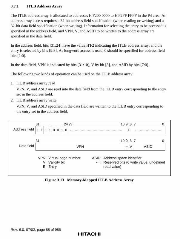
Rev. 6.0, 07/02, page 88 of 986
3.7.1 ITLB Address Array
The ITLB address array is allocated to addresses H'F200 0000 to H'F2FF FFFF in the P4 area. Anaddress array access requires a 32-bit address field specification (when reading or writing) and a32-bit data field specification (when writing). Information for selecting the entry to be accessed isspecified in the address field, and VPN, V, and ASID to be written to the address array arespecified in the data field.
In the address field, bits [31:24] have the value H'F2 indicating the ITLB address array, and theentry is selected by bits [9:8]. As longword access is used, 0 should be specified for address fieldbits [1:0].
In the data field, VPN is indicated by bits [31:10], V by bit [8], and ASID by bits [7:0].
The following two kinds of operation can be used on the ITLB address array:
1. ITLB address array read
VPN, V, and ASID are read into the data field from the ITLB entry corresponding to the entryset in the address field.
2. ITLB address array write
VPN, V, and ASID specified in the data field are written to the ITLB entry corresponding tothe entry set in the address field.
Address field31 23 0
1 1 1 1 0 0 1 0 E
Data field31 10 9 0
VVPN
VPN:V: E:
24
Virtual page numberValidity bitEntry
10 9 8 7
9 8 7
ASID
ASID::
Address space identifierReserved bits (0 write value, undefinedread value)
Figure 3.13 Memory-Mapped ITLB Address Array

Rev. 6.0, 07/02, page 89 of 986
3.7.2 ITLB Data Array 1
ITLB data array 1 is allocated to addresses H'F300 0000 to H'F37F FFFF in the P4 area. A dataarray access requires a 32-bit address field specification (when reading or writing) and a 32-bitdata field specification (when writing). Information for selecting the entry to be accessed isspecified in the address field, and PPN, V, SZ, PR, C, and SH to be written to the data array arespecified in the data field.
In the address field, bits [31:23] have the value H'F30 indicating ITLB data array 1, and the entryis selected by bits [9:8].
In the data field, PPN is indicated by bits [28:10], V by bit [8], SZ by bits [7] and [4], PR by bit[6], C by bit [3], and SH by bit [1].
The following two kinds of operation can be used on ITLB data array 1:
1. ITLB data array 1 read
PPN, V, SZ, PR, C, and SH are read into the data field from the ITLB entry corresponding tothe entry set in the address field.
2. ITLB data array 1 write
PPN, V, SZ, PR, C, and SH specified in the data field are written to the ITLB entrycorresponding to the entry set in the address field.
Address field31 23 0
1 1 1 1 0 0 01 1 E
Data field
PPN:V:E:
SZ:
24
Physical page numberValidity bitEntryPage size bits
10 9 8 7
PR:C:
SH::
Protection key dataCacheability bitShare status bitReserved bits (0 write value, undefinedread value)
31 2 1 0
V
10 9 8 730 29 28 4 36 5
SZ SHPR
CPPN
Figure 3.14 Memory-Mapped ITLB Data Array 1

Rev. 6.0, 07/02, page 90 of 986
3.7.3 ITLB Data Array 2
ITLB data array 2 is allocated to addresses H'F380 0000 to H'F3FF FFFF in the P4 area. A dataarray access requires a 32-bit address field specification (when reading or writing) and a 32-bitdata field specification (when writing). Information for selecting the entry to be accessed isspecified in the address field, and SA and TC to be written to data array 2 are specified in the datafield.
In the address field, bits [31:23] have the value H'F38 indicating ITLB data array 2, and the entryis selected by bits [9:8].
In the data field, SA is indicated by bits [2:0], and TC by bit [3].
The following two kinds of operation can be used on ITLB data array 2:
1. ITLB data array 2 read
SA and TC are read into the data field from the ITLB entry corresponding to the entry set inthe address field.
2. ITLB data array 2 write
SA and TC specified in the data field are written to the ITLB entry corresponding to the entryset in the address field.
Address field31 23 0
1 1 1 1 0 0 1 1 1 E
Data field31 4 0
TC: E:
24
Timing control bitEntry
89 7
3 2
SA::
Space attribute bitsReserved bits (0 write value, undefined read value)
10
SA
TC
Figure 3.15 Memory-Mapped ITLB Data Array 2
3.7.4 UTLB Address Array
The UTLB address array is allocated to addresses H'F600 0000 to H'F6FF FFFF in the P4 area. Anaddress array access requires a 32-bit address field specification (when reading or writing) and a32-bit data field specification (when writing). Information for selecting the entry to be accessed isspecified in the address field, and VPN, D, V, and ASID to be written to the address array arespecified in the data field.

Rev. 6.0, 07/02, page 91 of 986
In the address field, bits [31:24] have the value H'F6 indicating the UTLB address array, and theentry is selected by bits [13:8]. The address array bit [7] association bit (A bit) specifies whetheror not address comparison is performed when writing to the UTLB address array.
In the data field, VPN is indicated by bits [31:10], D by bit [9], V by bit [8], and ASID by bits[7:0].
The following three kinds of operation can be used on the UTLB address array:
1. UTLB address array read
VPN, D, V, and ASID are read into the data field from the UTLB entry corresponding to theentry set in the address field. In a read, associative operation is not performed regardless ofwhether the association bit specified in the address field is 1 or 0.
2. UTLB address array write (non-associative)
VPN, D, V, and ASID specified in the data field are written to the UTLB entry correspondingto the entry set in the address field. The A bit in the address field should be cleared to 0.
3. UTLB address array write (associative)
When a write is performed with the A bit in the address field set to 1, comparison of all theUTLB entries is carried out using the VPN specified in the data field and PTEH.ASID. Theusual address comparison rules are followed, but if a UTLB miss occurs, the result is nooperation, and an exception is not generated. If the comparison identifies a UTLB entrycorresponding to the VPN specified in the data field, D and V specified in the data field arewritten to that entry. If there is more than one matching entry, a data TLB multiple hitexception results. This associative operation is simultaneously carried out on the ITLB, and ifa matching entry is found in the ITLB, V is written to that entry. Even if the UTLBcomparison results in no operation, a write to the ITLB side only is performed as long as thereis an ITLB match. If there is a match in both the UTLB and ITLB, the UTLB information isalso written to the ITLB.
Address field
Data field
VPN:V:E:D:
Virtual page numberValidity bitEntryDirty bit
ASID:A:
:
Address space identifierAssociation bitReserved bits (0 write value, undefinedread value)
31 0
VD
10 9 8 730 29 28
A
8 7
ASIDVPN
31 23 2 1 0
1 1 1 1 0 1 1 0 E
24 14 13
Figure 3.16 Memory-Mapped UTLB Address Array

Rev. 6.0, 07/02, page 92 of 986
3.7.5 UTLB Data Array 1
UTLB data array 1 is allocated to addresses H'F700 0000 to H'F77F FFFF in the P4 area. A dataarray access requires a 32-bit address field specification (when reading or writing) and a 32-bitdata field specification (when writing). Information for selecting the entry to be accessed isspecified in the address field, and PPN, V, SZ, PR, C, D, SH, and WT to be written to the dataarray are specified in the data field.
In the address field, bits [31:23] have the value H'F70 indicating UTLB data array 1, and the entryis selected by bits [13:8].
In the data field, PPN is indicated by bits [28:10], V by bit [8], SZ by bits [7] and [4], PR by bits[6:5], C by bit [3], D by bit [2], SH by bit [1], and WT by bit [0].
The following two kinds of operation can be used on UTLB data array 1:
1. UTLB data array 1 read
PPN, V, SZ, PR, C, D, SH, and WT are read into the data field from the UTLB entrycorresponding to the entry set in the address field.
2. UTLB data array 1 write
PPN, V, SZ, PR, C, D, SH, and WT specified in the data field are written to the UTLB entrycorresponding to the entry set in the address field.
Address field
Data field
PPN:V:E:
SZ:D:
Physical page numberValidity bitEntryPage size bitsDirty bit
PR:C:
SH:WT:
:
Protection key dataCacheability bitShare status bitWrite-through bitReserved bits (0 write value, undefined read value)
31 2 1 0
V
10 9 8 730 29 28 4 36 5
PR CPPN
31 23 0
1 1 1 1 0 1 1 1 0 E
24 8 714 13
D
SZ SH WT
Figure 3.17 Memory-Mapped UTLB Data Array 1

Rev. 6.0, 07/02, page 93 of 986
3.7.6 UTLB Data Array 2
UTLB data array 2 is allocated to addresses H'F780 0000 to H'F7FF FFFF in the P4 area. A dataarray access requires a 32-bit address field specification (when reading or writing) and a 32-bitdata field specification (when writing). Information for selecting the entry to be accessed isspecified in the address field, and SA and TC to be written to data array 2 are specified in the datafield.
In the address field, bits [31:23] have the value H'F78 indicating UTLB data array 2, and the entryis selected by bits [13:8].
In the data field, TC is indicated by bit [3], and SA by bits [2:0].
The following two kinds of operation can be used on UTLB data array 2:
1. UTLB data array 2 read
SA and TC are read into the data field from the UTLB entry corresponding to the entry set inthe address field.
2. UTLB data array 2 write
SA and TC specified in the data field are written to the UTLB entry corresponding to the entryset in the address field.
Address field31 23 0
1 1 1 1 0 1 1 1 1 E
Data field31 4 0
TC
24 813 7
3 2
14
SA
TC: E:
Timing control bitEntry
SA::
Space attribute bitsReserved bits (0 write value, undefined readvalue)
Figure 3.18 Memory-Mapped UTLB Data Array 2

Rev. 6.0, 07/02, page 94 of 986

Rev. 6.0, 07/02, page 95 of 986
Section 4 Caches
4.1 Overview
4.1.1 Features
An SH7750 or SH7750S has an on-chip 8-kbyte instruction cache (IC) for instructions and 16-kbyte operand cache (OC) for data. Half of the memory of the operand cache (8 kbytes) mayalternatively be used as on-chip RAM. The features of this cache are summarized in table 4.1
The SH7750R has an on-chip 16-kbyte instruction cache (IC) for instructions and 32-kbyteoperand cache (OC) for data. Half of the memory of the operand cache (16 kbytes) mayalternatively be used as on-chip RAM. When the EMODE bit of the CCR register is 0, theSH7750R’s cache is set to operate in the SH7750/SH7750S-compatible mode and behaves asshown in table 4.1. The features of the cache when the EMODE bit in the CCR register is 1 aregiven in table 4.2. The EMODE bit is initialized to 0 after a power-on reset or manual reset.
For high-speed writing to external memories, the SH7750 series supports 32 bytes × 2 of storequeues (SQ). Table 4.3 lists the features of these SQs.
Table 4.1 Cache Features (SH7750, SH7750S)
Item Instruction Cache Operand Cache
Capacity 8-kbyte cache 16-kbyte cache or 8-kbyte cache +8-kbyte RAM
Type Direct mapping Direct mapping
Line size 32 bytes 32 bytes
Entries 256 512
Write method Copy-back/write-through selectable
Table 4.2 Cache Features (SH7750R)
Item Instruction Cache Operand Cache
Capacity 16-kbyte cache 32-kbyte cache or 16-kbyte cache +16-kbyte RAM
Type 2-way set-associative 2-way set-associative
Line size 32 bytes 32 bytes
Entries 256 entries/way 512 entries/way
Write method Copy-back/write-through selectable
Replacement method LRU (least-recently-used) algorithm LRU algorithm

Rev. 6.0, 07/02, page 96 of 986
Table 4.3 Features of Store Queues
Item Store Queues
Capacity 2 × 32 bytes
Addresses H'E000 0000 to H'E3FF FFFF
Write Store instruction (1-cycle write)
Write-back Prefetch instruction (PREF instruction)
Access right MMU off: according to MMUCR.SQMD
MMU on: according to individual page PR
4.1.2 Register Configuration
Table 4.4 shows the cache control registers.
Table 4.4 Cache Control Registers
Name Abbreviation R/WInitialValue*1
P4Address*2
Area 7Address*2
AccessSize
Cache controlregister
CCR R/W H'0000 0000 H'FF00 001C H'1F00 001C 32
Queue addresscontrol register 0
QACR0 R/W Undefined H'FF00 0038 H'1F00 0038 32
Queue addresscontrol register 1
QACR1 R/W Undefined H'FF00 003C H'1F00 003C 32
Notes: *1 The initial value is the value after a power-on or manual reset.*2 This is the address when using the virtual/physical address space P4 area. The area 7
address is the address used when making an access from physical address space area7 using the TLB.

Rev. 6.0, 07/02, page 97 of 986
4.2 Register Descriptions
There are three cache and store queue related control registers, as shown in figure 4.1.
CCR
31 30 1416 15 12 11 10 9 8 7 6 5 4 3 2
CB
1 0
ICI ICE ORAOIX OCI
AREA
indicates reserved bits: 0 must be specified in a write; the read value is 0.
WT OCEIIXEMODE*
QACR0
31 5 4 2 1 0
AREA
QACR1
31 5 4 2 1 0
*: SH7750R only
Figure 4.1 Cache and Store Queue Control Registers
(1) Cache Control Register (CCR): CCR contains the following bits:
EMODE: Double-sized cache mode (Only for SH7750R; reserved bit for SH7750 and SH7750S)IIX: IC index enableICI: IC invalidationICE: IC enableOIX: OC index enableORA: OC RAM enableOCI: OC invalidationCB: Copy-back enableWT: Write-through enableOCE: OC enable
Longword access to CCR can be performed from H'FF00 001C in the P4 area and H'1F00 001C inarea 7. The CCR bits are used for the cache settings described below. Consequently, CCRmodifications must only be made by a program in the non-cached P2 area. After CCR is updated,an instruction that performs data access to the P0, P1, P3, or U0 area should be located at leastfour instructions after the CCR update instruction. Also, a branch instruction to the P0, P1, P3, orU0 area should be located at least eight instructions after the CCR update instruction.

Rev. 6.0, 07/02, page 98 of 986
• EMODE: Double-sized cache mode bit
In the SH7750R, this bit indicates whether the double-sized cache mode is used or not.
This bit is reserved in the SH7750 and SH7750S. The EMODE bit must not be written to whilethe cache is being used.
0: SH7750/SH7750S-compatible mode*1 (initial value)
1: Double-sized cache mode
• IIX: IC index enable bit
0: Effective address bits [12:5] used for IC entry selection
1: Effective address bits [25] and [11:5] used for IC entry selection
• ICI: IC invalidation bit
When 1 is written to this bit, the V bits of all IC entries are cleared to 0. This bit always returns0 when read.
• ICE: IC enable bit
Indicates whether or not the IC is to be used. When address translation is performed, the ICcannot be used unless the C bit in the page management information is also 1.
0: IC not used
1: IC used
• OIX: OC index enable bit*2
0: Effective address bits [13:5] used for OC entry selection
1: Effective address bits [25] and [12:5] used for OC entry selection
• ORA: OC RAM enable bit*3
When the OC is enabled (OCE = 1), the ORA bit specifies whether the half of the OC are to beused as RAM. When the OC is not enabled (OCE = 0), the ORA bit should be cleared to 0.
0: Normal mode (the entire OC is used as a cache)
1: RAM mode (half of the OC is used as a cache and the other half is used as RAM)
• OCI: OC invalidation bit
When 1 is written to this bit, the V and U bits of all OC entries are cleared to 0. This bit alwaysreturns 0 when read.
• CB: Copy-back bit
Indicates the P1 area cache write mode.
0: Write-through mode
1: Copy-back mode

Rev. 6.0, 07/02, page 99 of 986
• WT: Write-through bit
Indicates the P0, U0, and P3 area cache write mode. When address translation is performed,the value of the WT bit in the page management information has priority.
0: Copy-back mode
1: Write-through mode
• OCE: OC enable bit
Indicates whether or not the OC is to be used. When address translation is performed, the OCcannot be used unless the C bit in the page management information is also 1.
0: OC not used
1: OC used
Note: *1 No compatibility for RAM mode in OC index mode and address assignment in RAMmode.
*2 When the ORA bit is 1 in the SH7750R, the OIX bit should be cleared to 0.
*3 When the OIX bit in the SH7750R is 1, the ORA bit should be cleared to 0.
(2) Queue Address Control Register 0 (QACR0): Longword access to QACR0 can beperformed from H'FF00 0038 in the P4 area and H'1F00 0038 in area 7. QACR0 specifies the areaonto which store queue 0 (SQ0) is mapped when the MMU is off.
(3) Queue Address Control Register 1 (QACR1): Longword access to QACR1 can beperformed from H'FF00 003C in the P4 area and H'1F00 003C in area 7. QACR1 specifies thearea onto which store queue 1 (SQ1) is mapped when the MMU is off.
4.3 Operand Cache (OC)
4.3.1 Configuration
The operand cache of the SH7750 or SH7750S is of the direct-mapping type and consists of 512cache lines, each composed of a 19-bit tag, V bit, U bit, and 32-byte data. The SH7750R’soperand cache is 2-way set-associative. Each way consists of 512 cache lines.
Figure 4.2 shows the configuration of the operand cache for the SH7750 and SH7750S.
Figure 4.3 shows the configuration of the operand cache for the SH7750R.

Rev. 6.0, 07/02, page 100 of 986
31 26 25 5 4 3 2 1
LW0
32 bits
LW1
32 bits
LW2
32 bits
LW3
32 bits
LW4
32 bits
LW5
32 bits
LW6
32 bits
LW7
32 bits
MMU
RAM areadetermination
ORAOIX[13] [12]
[11:5]
511 19 bits 1 bit 1 bit
Tag U V
Address array Data array
Ent
ry s
elec
tion
Longword (LW) selection
Effective address
39
22
19
0
Write dataRead data
Hit signal
Compare
13 12 11 10 9 0
Figure 4.2 Configuration of Operand Cache(SH7750, SH7750S)

Rev. 6.0, 07/02, page 101 of 986
31 26 25 5 4 2
LW0
32 bits
LW1
32 bits
LW2
32 bits
LW3
32 bits
LW4
32 bits
LW5
32 bits
LW6
32 bits
LW7
32 bits 1 bit
MMU
RAM areajudgment
OIXORA [13]
[12:5]
511 19 bits 1 bit 1 bit
Tag address U V
Address array(way 0, way 1) Data array (way 0, way 1)
LRU
Entry selection
Longword (LW)selection
Effective address
3922
19
0
Write dataRead data
Hit signal
Compareway 0
Compareway 1
13 12 10 0
Figure 4.3 Configuration of Operand Cache (SH7750R)

Rev. 6.0, 07/02, page 102 of 986
• Tag
Stores the upper 19 bits of the 29-bit external memory address of the data line to be cached.The tag is not initialized by a power-on or manual reset.
• V bit (validity bit)
Indicates that valid data is stored in the cache line. When this bit is 1, the cache line data isvalid. The V bit is initialized to 0 by a power-on reset, but retains its value in a manual reset.
• U bit (dirty bit)
The U bit is set to 1 if data is written to the cache line while the cache is being used in copy-back mode. That is, the U bit indicates a mismatch between the data in the cache line and thedata in external memory. The U bit is never set to 1 while the cache is being used in write-through mode, unless it is modified by accessing the memory-mapped cache (see section 4.5,Memory-Mapped Cache Configuration). The U bit is initialized to 0 by a power-on reset, butretains its value in a manual reset.
• Data field
The data field holds 32 bytes (256 bits) of data per cache line. The data array is not initializedby a power-on or manual reset.
• LRU (SH7750R only)
In a 2-way set-associative cache, up to 2 items of data can be registered in the cache at eachentry address (address: 13–5). When an entry is registered, the LRU bit indicates which of the2 ways it is to be registered in. The LRU bit is a single bit of each entry, and its value iscontrolled by hardware.
The LRU (least-recently-used) algorithm is used for way selection, and selects the less recentlyaccessed way. The LRU bits are initialized to 0 by a power-on reset but not by a manual reset.The LRU bits cannot be read or written by software.

Rev. 6.0, 07/02, page 103 of 986
4.3.2 Read Operation
When the OC is enabled (CCR.OCE = 1) and data is read by means of an effective address from acacheable area, the cache operates as follows:
1. The tag, V bit, and U bit are read from the cache line indexed by effective address bits [13:5].
2. The tag is compared with bits [28:10] of the address resulting from effective addresstranslation by the MMU:
• If the tag matches and the V bit is 1 → (3a)
• If the tag matches and the V bit is 0 → (3b)
• If the tag does not match and the V bit is 0 → (3b)
• If the tag does not match, the V bit is 1, and the U bit is 0 → (3b)
• If the tag does not match, the V bit is 1, and the U bit is 1 → (3c)
3a. Cache hit
The data indexed by effective address bits [4:0] is read from the data field of the cache lineindexed by effective address bits [13:5] in accordance with the access size(quadword/longword/word/byte).
3b. Cache miss (no write-back)
Data is read into the cache line from the external memory space corresponding to the effectiveaddress. Data reading is performed, using the wraparound method, in order from the longworddata corresponding to the effective address, and when the corresponding data arrives in thecache, the read data is returned to the CPU. While the remaining one cache line of data is beingread, the CPU can execute the next processing. When reading of one line of data is completed,the tag corresponding to the effective address is recorded in the cache, and 1 is written to the Vbit.
3c. Cache miss (with write-back)
The tag and data field of the cache line indexed by effective address bits [13:5] are saved in thewrite-back buffer. Then data is read into the cache line from the external memory spacecorresponding to the effective address. Data reading is performed, using the wraparoundmethod, in order from the longword data corresponding to the effective address, and when thecorresponding data arrives in the cache, the read data is returned to the CPU. While theremaining one cache line of data is being read, the CPU can execute the next processing. Whenreading of one line of data is completed, the tag corresponding to the effective address isrecorded in the cache, 1 is written to the V bit, and 0 to the U bit. The data in the write-backbuffer is then written back to external memory.

Rev. 6.0, 07/02, page 104 of 986
4.3.3 Write Operation
When the OC is enabled (CCR.OCE = 1) and data is written by means of an effective address to acacheable area, the cache operates as follows:
1. The tag, V bit, and U bit are read from the cache line indexed by effective address bits [13:5].
2. The tag is compared with bits [28:10] of the address resulting from effective addresstranslation by the MMU:
Copy-back Write-through
• If the tag matches and the V bit is 1 → (3a) → (3b)
• If the tag matches and the V bit is 0 → (3c) → (3d)
• If the tag does not match and the V bit is 0 → (3c) → (3d)
• If the tag does not match, the V bit is 1, and the U bit is 0 → (3c) → (3d)
• If the tag does not match, the V bit is 1, and the U bit is 1 → (3e) → (3d)
3a. Cache hit (copy-back)
A data write in accordance with the access size (quadword/longword/word/byte) is performedfor the data indexed by bits [4:0] of the effective address of the data field of the cache lineindexed by effective address bits [13:5]. Then 1 is set in the U bit.
3b. Cache hit (write-through)
A data write in accordance with the access size (quadword/longword/word/byte) is performedfor the data indexed by bits [4:0] of the effective address of the data field of the cache lineindexed by effective address bits [13:5]. A write is also performed to the correspondingexternal memory using the specified access size.
3c. Cache miss (no copy-back/write-back)
A data write in accordance with the access size (quadword/longword/word/byte) is performedfor the data indexed by bits [4:0] of the effective address of the data field of the cache lineindexed by effective address bits [13:5]. Then, data is read into the cache line from the externalmemory space corresponding to the effective address. Data reading is performed, using thewraparound method, in order from the longword data corresponding to the effective address,and one cache line of data is read excluding the written data. During this time, the CPU canexecute the next processing. When reading of one line of data is completed, the tagcorresponding to the effective address is recorded in the cache, and 1 is written to the V bit andU bit.
3d. Cache miss (write-through)
A write of the specified access size is performed to the external memory corresponding to theeffective address. In this case, a write to cache is not performed.
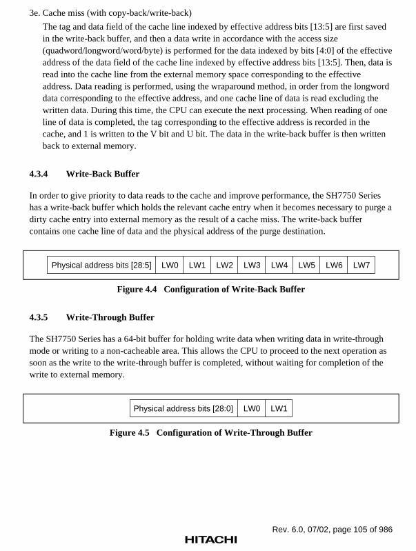
Rev. 6.0, 07/02, page 105 of 986
3e. Cache miss (with copy-back/write-back)
The tag and data field of the cache line indexed by effective address bits [13:5] are first savedin the write-back buffer, and then a data write in accordance with the access size(quadword/longword/word/byte) is performed for the data indexed by bits [4:0] of the effectiveaddress of the data field of the cache line indexed by effective address bits [13:5]. Then, data isread into the cache line from the external memory space corresponding to the effectiveaddress. Data reading is performed, using the wraparound method, in order from the longworddata corresponding to the effective address, and one cache line of data is read excluding thewritten data. During this time, the CPU can execute the next processing. When reading of oneline of data is completed, the tag corresponding to the effective address is recorded in thecache, and 1 is written to the V bit and U bit. The data in the write-back buffer is then writtenback to external memory.
4.3.4 Write-Back Buffer
In order to give priority to data reads to the cache and improve performance, the SH7750 Serieshas a write-back buffer which holds the relevant cache entry when it becomes necessary to purge adirty cache entry into external memory as the result of a cache miss. The write-back buffercontains one cache line of data and the physical address of the purge destination.
LW7Physical address bits [28:5] LW6LW5LW4LW3LW2LW1LW0
Figure 4.4 Configuration of Write-Back Buffer
4.3.5 Write-Through Buffer
The SH7750 Series has a 64-bit buffer for holding write data when writing data in write-throughmode or writing to a non-cacheable area. This allows the CPU to proceed to the next operation assoon as the write to the write-through buffer is completed, without waiting for completion of thewrite to external memory.
Physical address bits [28:0] LW1LW0
Figure 4.5 Configuration of Write-Through Buffer

Rev. 6.0, 07/02, page 106 of 986
4.3.6 RAM Mode
Setting CCR.ORA to 1 enables half of the operand cache to be used as RAM. In the SH7750 orSH7750S, the 8 kbytes of operand cache entries 128 to 255 and 384 to 511 are used as RAM. Inthe SH7750/SH7750S-compatible mode of the SH7750R, the 8-kbyte area otherwise used for OCentries 256 to 511 is designated as a RAM area. In the double-sized cache mode of the SH7750R,a total of 16 kbytes, comprising entries 256 to 511 in both of the ways of the operand cache, isdesignated as a RAM area. Other entries can still be used as cache. RAM can be accessed usingaddresses H'7C00 0000 to H'7FFF FFFF. Byte-, word-, longword-, and quadword-size data readsand writes can be performed in the operand cache RAM area. Instruction fetches cannot beperformed in this area. With the SH7750R, the OC index mode is not available in RAM mode.
An example of RAM use in the SH7750 or SH7750S is shown below. Here, the 4 kbytescomprising OC entries 128 to 255 are designated as RAM area 1, and the 4 kbytes comprising OCentries 384 to 511 as RAM area 2.
• When OC index mode is off (CCR.OIX = 0)
H'7C00 0000 to H'7C00 0FFF (4 kB): Corresponds to RAM area 1
H'7C00 1000 to H'7C00 1FFF (4 kB): Corresponds to RAM area 1
H'7C00 2000 to H'7C00 2FFF (4 kB): Corresponds to RAM area 2
H'7C00 3000 to H'7C00 3FFF (4 kB): Corresponds to RAM area 2
H'7C00 4000 to H'7C00 4FFF (4 kB): Corresponds to RAM area 1
: : :
RAM areas 1 and 2 in the SH7750 or SH7750S then repeat every 8 kbytes up to H'7FFF FFFF.
Thus, to secure a continuous 8-kbyte RAM area, the area from H'7C00 1000 to H'7C00 2FFFcan be used, for example.
• When OC index mode is on (CCR.OIX = 1)
H'7C00 0000 to H'7C00 0FFF (4 kB): Corresponds to RAM area 1
H'7C00 1000 to H'7C00 1FFF (4 kB): Corresponds to RAM area 1
H'7C00 2000 to H'7C00 2FFF (4 kB): Corresponds to RAM area 1
: : :
H'7DFF F000 to H'7DFF FFFF (4 kB): Corresponds to RAM area 1
H'7E00 0000 to H'7E00 0FFF (4 kB): Corresponds to RAM area 2
H'7E00 1000 to H'7E00 1FFF (4 kB): Corresponds to RAM area 2
: : :
H'7FFF F000 to H'7FFF FFFF (4 kB): Corresponds to RAM area 2
As the distinction between RAM areas 1 and 2 is indicated by address bit [25], the area fromH'7DFF F000 to H'7E00 0FFF should be used to secure a continuous 8-kbyte RAM area.

Rev. 6.0, 07/02, page 107 of 986
Examples of RAM usage with the SH7750R is shown below.
• In SH7750/SH7750S-compatible mode (CCR.EMODE = 0)
H'7C00 0000 to H'7C00 1FFF (8 kB): RAM area (entries 256 to 511)
H'7C00 2000 to H'7C00 3FFF (8 kB): RAM area (entries 256 to 511)
: : :
In the same pattern, shadows of the RAM area are created in 8-kbyte blocks until H'7FFFFFFF is reached.
• In double-sized cache mode (CCR.EMODE = 1)
In this mode, the 8 kbytes comprising entries 256 to 511 of OC way 0 are designated as RAMarea 1 and the 8-kbytes comprising entries 256 to 511 of OC way 1 are designated as RAMarea 2.
H'7C00 0000 to H'7C00 1FFF (8 kB): Corresponds to RAM area 1
H'7C00 2000 to H'7C00 3FFF (8 kB): Corresponds to RAM area 2
H'7C00 4000 to H'7C00 5FFF (8 kB): Corresponds to RAM area 1
H'7C00 6000 to H'7C00 7FFF (8 kB): Corresponds to RAM area 2
: : :
In the same pattern, shadows of the RAM area are created in 16-kbyte blocks until H'7FFFFFFF is reached.
4.3.7 OC Index Mode
Setting CCR.OIX to 1 enables OC indexing to be performed using bit [25] of the effectiveaddress. This is called OC index mode. In normal mode, with CCR.OIX cleared to 0, OC indexingis performed using bits [13:5] of the effective address. Using index mode allows the OC to behandled as two areas by means of effective address bit [25], providing efficient use of the cache.The SH7750R cannot be used in RAM mode when OC index mode is selected.
4.3.8 Coherency between Cache and External Memory
Coherency between cache and external memory should be assured by software. In the SH7750Series, the following four new instructions are supported for cache operations. Details of theseinstructions are given in the Programming Manual.
Invalidate instruction: OCBI @Rn Cache invalidation (no write-back)
Purge instruction: OCBP @Rn Cache invalidation (with write-back)
Write-back instruction: OCBWB @Rn Cache write-back
Allocate instruction: MOVCA.L R0,@Rn Cache allocation

Rev. 6.0, 07/02, page 108 of 986
4.3.9 Prefetch Operation
The SH7750 Series supports a prefetch instruction to reduce the cache fill penalty incurred as theresult of a cache miss. If it is known that a cache miss will result from a read or write operation, itis possible to fill the cache with data beforehand by means of the prefetch instruction to prevent acache miss due to the read or write operation, and so improve software performance. If a prefetchinstruction is executed for data already held in the cache, or if the prefetch address results in aUTLB miss or a protection violation, the result is no operation, and an exception is not generated.Details of the prefetch instruction are given in the Programming Manual.
Prefetch instruction: PREF @Rn
4.4 Instruction Cache (IC)
4.4.1 Configuration
The instruction cache of the SH7750 or SH7750S is of the direct-mapping type and consists of256 cache lines, each composed of a 19-bit tag, V bit, and 32-byte data (16 instructions). TheSH7750R’s instruction cache is 2-way set associative. Each way consists of 256 cache lines.
Figure 4.6 shows the configuration of the instruction cache for the SH7750 and SH7750S.
Figure 4.7 shows the configuration of the instruction cache for the SH7750R.

Rev. 6.0, 07/02, page 109 of 986
LW0
32 bits
LW1
32 bits
LW2
32 bits
LW3
32 bits
LW4
32 bits
LW5
32 bits
LW6
32 bits
LW7
32 bits255 19 bits 1 bit
Tag V
Address array
Longword (LW) selection
Data array
0
Read data
Hit signal
Compare
31 26 25 5 4 3 2 1
MMU
IIX[12]
[11:5]E
ntry
sel
ectio
n
Effective address
8 3
22
19
13 12 11 10 9 0
Figure 4.6 Configuration of Instruction Cache (SH7750, SH7750S)

Rev. 6.0, 07/02, page 110 of 986
31 25 5 4 2
LW0
32 bits
LW1
32 bits
LW2
32 bits
LW3
32 bits
LW4
32 bits
LW5
32 bits
LW6
32 bits
LW7
32 bits 1 bit
MMU
IIX[12]
[11:5]
255 19 bits 1 bit
Tag address V
Address array(way 0, way1)
Longword (LW)selection
LRU
Entry selection
Data array (way 0, way 1)
Effective address
38
22
19
0
Read data
Hit signal
Compareway 0
Compareway 1
13 12 11 10 0
Figure 4.7 Configuration of Instruction Cache (SH7750R)
• Tag
Stores the upper 19 bits of the 29-bit external address of the data line to be cached. The tag isnot initialized by a power-on or manual reset.
• V bit (validity bit)
Indicates that valid data is stored in the cache line. When this bit is 1, the cache line data isvalid. The V bit is initialized to 0 by a power-on reset, but retains its value in a manual reset.
• Data array
The data field holds 32 bytes (256 bits) of data per cache line. The data array is not initializedby a power-on or manual reset.

Rev. 6.0, 07/02, page 111 of 986
• LRU (SH7750R only)
In a 2-way set-associative cache, up to 2 items of data can be registered in the cache at eachentry address (address: 12–5). When an entry is registered, the LRU bit indicates which of the2 ways it is to be registered in. The LRU bit is a single bit of each entry, and its usage iscontrolled by hardware.
The LRU (least-recently-used) algorithm is used for way selection, and selects the less recentlyaccessed way. The LRU bits are initialized to 0 by a power-on reset but not by a manual reset.The LRU bits cannot be read or written by software.
4.4.2 Read Operation
When the IC is enabled (CCR.ICE = 1) and instruction fetches are performed by means of aneffective address from a cacheable area, the instruction cache operates as follows:
1. The tag and V bit are read from the cache line indexed by effective address bits [12:5].
2. The tag is compared with bits [28:10] of the address resulting from effective addresstranslation by the MMU:
• If the tag matches and the V bit is 1 → (3a)
• If the tag matches and the V bit is 0 → (3b)
• If the tag does not match and the V bit is 0 → (3b)
• If the tag does not match and the V bit is 1 → (3b)
3a. Cache hit
The data indexed by effective address bits [4:2] is read as an instruction from the data field ofthe cache line indexed by effective address bits [12:5].
3b. Cache miss
Data is read into the cache line from the external memory space corresponding to the effectiveaddress. Data reading is performed, using the wraparound method, in order from the longworddata corresponding to the effective address, and when the corresponding data arrives in thecache, the read data is returned to the CPU as an instruction. When reading of one line of datais completed, the tag corresponding to the effective address is recorded in the cache, and 1 iswritten to the V bit.
4.4.3 IC Index Mode
Setting CCR.IIX to 1 enables IC indexing to be performed using bit [25] of the effective address.This is called IC index mode. In normal mode, with CCR.IIX cleared to 0, IC indexing isperformed using bits [12:5] of the effective address. Using index mode allows the IC to be handledas two areas by means of effective address bit [25], providing efficient use of the cache.

Rev. 6.0, 07/02, page 112 of 986
4.5 Memory-Mapped Cache Configuration (SH7750, SH7750S)
To enable the IC and OC to be managed by software, their contents can be read and written by aP2 area program with a MOV instruction in privileged mode. Operation is not guaranteed if accessis made from a program in another area. In this case, a branch to the P0, U0, P1, or P3 area shouldbe made at least 8 instructions after this MOV instruction. The IC and OC are allocated to the P4area in physical memory space. Only data accesses can be used on both the IC address array anddata array and the OC address array and data array, and accesses are always longword-size.Instruction fetches cannot be performed in these areas. For reserved bits, a write value of 0 shouldbe specified; their read value is undefined.
4.5.1 IC Address Array
The IC address array is allocated to addresses H'F000 0000 to H'F0FF FFFF in the P4 area. Anaddress array access requires a 32-bit address field specification (when reading or writing) and a32-bit data field specification. The entry to be accessed is specified in the address field, and thewrite tag and V bit are specified in the data field.
In the address field, bits [31:24] have the value H'F0 indicating the IC address array, and the entryis specified by bits [12:5]. CCR.IIX has no effect on this entry specification. The address array bit[3] association bit (A bit) specifies whether or not association is performed when writing to the ICaddress array. As only longword access is used, 0 should be specified for address field bits [1:0].
In the data field, the tag is indicated by bits [31:10], and the V bit by bit [0]. As the IC addressarray tag is 19 bits in length, data field bits [31:29] are not used in the case of a write in whichassociation is not performed. Data field bits [31:29] are used for the virtual address specificationonly in the case of a write in which association is performed.
The following three kinds of operation can be used on the IC address array:
1. IC address array read
The tag and V bit are read into the data field from the IC entry corresponding to the entry set inthe address field. In a read, associative operation is not performed regardless of whether theassociation bit specified in the address field is 1 or 0.
2. IC address array write (non-associative)
The tag and V bit specified in the data field are written to the IC entry corresponding to theentry set in the address field. The A bit in the address field should be cleared to 0.
3. IC address array write (associative)
When a write is performed with the A bit in the address field set to 1, the tag stored in theentry specified in the address field is compared with the tag specified in the data field. If theMMU is enabled at this time, comparison is performed after the virtual address specified bydata field bits [31:10] has been translated to a physical address using the ITLB. If the addressesmatch and the V bit is 1, the V bit specified in the data field is written into the IC entry. In

Rev. 6.0, 07/02, page 113 of 986
other cases, no operation is performed. This operation is used to invalidate a specific IC entry.If an ITLB miss occurs during address translation, or the comparison shows a mismatch, aninterrupt is not generated, no operation is performed, and the write is not executed. If aninstruction TLB multiple hit exception occurs during address translation, processing switchesto the instruction TLB multiple hit exception handling routine.
Address field31 23 12 5 4 3 2 1 0
1 1 1 1 0 0 0 0 Entry A
Data field31 10 9 1 0
VTag
VA
24 13
: Validity bit: Association bit: Reserved bits (0 write value, undefined read value)
Figure 4.8 Memory-Mapped IC Address Array
4.5.2 IC Data Array
The IC data array is allocated to addresses H'F100 0000 to H'F1FF FFFF in the P4 area. A dataarray access requires a 32-bit address field specification (when reading or writing) and a 32-bitdata field specification. The entry to be accessed is specified in the address field, and the longworddata to be written is specified in the data field.
In the address field, bits [31:24] have the value H'F1 indicating the IC data array, and the entry isspecified by bits [12:5]. CCR.IIX has no effect on this entry specification. Address field bits [4:2]are used for the longword data specification in the entry. As only longword access is used, 0should be specified for address field bits [1:0].
The data field is used for the longword data specification.
The following two kinds of operation can be used on the IC data array:
1. IC data array read
Longword data is read into the data field from the data specified by the longword specificationbits in the address field in the IC entry corresponding to the entry set in the address field.
2. IC data array write
The longword data specified in the data field is written for the data specified by the longwordspecification bits in the address field in the IC entry corresponding to the entry set in theaddress field.

Rev. 6.0, 07/02, page 114 of 986
Address field31 23 12 5 4 2 1 0
1 1 1 1 0 0 0 1 Entry L
Data field31 0
Longword data
L
24 13
: Longword specification bits: Reserved bits (0 write value, undefined read value)
Figure 4.9 Memory-Mapped IC Data Array
4.5.3 OC Address Array
The OC address array is allocated to addresses H'F400 0000 to H'F4FF FFFF in the P4 area. Anaddress array access requires a 32-bit address field specification (when reading or writing) and a32-bit data field specification. The entry to be accessed is specified in the address field, and thewrite tag, U bit, and V bit are specified in the data field.
In the address field, bits [31:24] have the value H'F4 indicating the OC address array, and theentry is specified by bits [13:5]. CCR.OIX and CCR.ORA have no effect on this entryspecification. The address array bit [3] association bit (A bit) specifies whether or not associationis performed when writing to the OC address array. As only longword access is used, 0 should bespecified for address field bits [1:0].
In the data field, the tag is indicated by bits [31:10], the U bit by bit [1], and the V bit by bit [0].As the OC address array tag is 19 bits in length, data field bits [31:29] are not used in the case of awrite in which association is not performed. Data field bits [31:29] are used for the virtual addressspecification only in the case of a write in which association is performed.
The following three kinds of operation can be used on the OC address array:
1. OC address array read
The tag, U bit, and V bit are read into the data field from the OC entry corresponding to theentry set in the address field. In a read, associative operation is not performed regardless ofwhether the association bit specified in the address field is 1 or 0.
2. OC address array write (non-associative)
The tag, U bit, and V bit specified in the data field are written to the OC entry corresponding tothe entry set in the address field. The A bit in the address field should be cleared to 0.
When a write is performed to a cache line for which the U bit and V bit are both 1, after write-back of that cache line, the tag, U bit, and V bit specified in the data field are written.

Rev. 6.0, 07/02, page 115 of 986
3. OC address array write (associative)
When a write is performed with the A bit in the address field set to 1, the tag stored in theentry specified in the address field is compared with the tag specified in the data field. If theMMU is enabled at this time, comparison is performed after the virtual address specified bydata field bits [31:10] has been translated to a physical address using the UTLB. If theaddresses match and the V bit is 1, the U bit and V bit specified in the data field are writteninto the OC entry. This operation is used to invalidate a specific OC entry. In other cases, nooperation is performed. If the OC entry U bit is 1, and 0 is written to the V bit or to the U bit,write-back is performed. If an UTLB miss occurs during address translation, or the comparisonshows a mismatch, an exception is not generated, no operation is performed, and the write isnot executed. If a data TLB multiple hit exception occurs during address translation,processing switches to the data TLB multiple hit exception handling routine.
Address field31 23 5 4 3 2 1 0
1 1 1 1 0 1 0 0 Entry A
Data field31 10 9 1 0
VTag
24 1314
2
U
VUA
: Validity bit: Dirty bit: Association bit: Reserved bits (0 write value, undefined read value)
Figure 4.10 Memory-Mapped OC Address Array
4.5.4 OC Data Array
The OC data array is allocated to addresses H'F500 0000 to H'F5FF FFFF in the P4 area. A dataarray access requires a 32-bit address field specification (when reading or writing) and a 32-bitdata field specification. The entry to be accessed is specified in the address field, and the longworddata to be written is specified in the data field.
In the address field, bits [31:24] have the value H'F5 indicating the OC data array, and the entry isspecified by bits [13:5]. CCR.OIX and CCR.ORA have no effect on this entry specification.Address field bits [4:2] are used for the longword data specification in the entry. As only longwordaccess is used, 0 should be specified for address field bits [1:0].
The data field is used for the longword data specification.

Rev. 6.0, 07/02, page 116 of 986
The following two kinds of operation can be used on the OC data array:
1. OC data array read
Longword data is read into the data field from the data specified by the longword specificationbits in the address field in the OC entry corresponding to the entry set in the address field.
2. OC data array write
The longword data specified in the data field is written for the data specified by the longwordspecification bits in the address field in the OC entry corresponding the entry set in the addressfield. This write does not set the U bit to 1 on the address array side.
Address field31 23 5 4 2 1 0
1 1 1 1 0 1 0 1 Entry L
Data field31 0
Longword data
24 1314
L : Longword specification bits: Reserved bits (0 write value, undefined read value)
Figure 4.11 Memory-Mapped OC Data Array
4.6 Memory-Mapped Cache Configuration (SH7750R)
To enable the management of the IC and OC by software, a program running in the privilegedmode is allowed to access their contents.
The contents of IC can be read and written by using MOV instructions in a P2-area programrunning in the privileged mode. Operation is not guaranteed for access from a program in someother area. Any branching to other areas must take place at least 8 instructions after this MOVinstruction.
The contents of IC can be read and written by using MOV instructions in a P1- or P2-areaprogram running in the privileged mode. Operation is not guaranteed if access is attempted from aprogram running in some other area. A branch to the P0, U0, or P3 area must be made at least 8instructions after this MOV instruction.
The IC and OC are allocated to the P4 area of the physical memory space. The address and dataarrays of both the IC and OC are only accessible by their data fields. Longword operations mustbe used. Instruction fetches from these areas are not possible. For reserved bits, a write value of 0should be specified; values read from such bits are undefined. Note that, in the SH7750/SH7750S-compatible mode, the configuration of the SH7750R’s memory-mapped cache is the same as thatof the SH7750 or SH7750S.

Rev. 6.0, 07/02, page 117 of 986
4.6.1 IC Address Array
The IC address array is allocated to addresses H'F000 0000 to H'F0FF FFFF in the P4 area. Anaddress array access requires a 32-bit address field specification (when reading or writing) and a32-bit data field specification. The way and entry to be accessed is specified in the address field,and the write tag and V bit are specified in the data field.
In the address field, bits [31:24] have the value H'F0 indicating the IC address array, the way isspecified by bit [13], and the entry by bits [12:5]. CCR.IIX has no effect on this entryspecification. The address array bit [3] association bit (A bit) specifies whether or not associationis performed when writing to the IC address array. As only longword access is used, 0 should bespecified for address field bits [1:0].
In the data field, the tag is indicated by bits [31:10], and the V bit by bit [0]. As the IC addressarray tag is 19 bits in length, data field bits [31:29] are not used in the case of a write in whichassociation is not performed. Data field bits [31:29] are used for the virtual address specificationonly in the case of a write in which association is performed.
The following three kinds of operation can be used on the IC address array:
1. IC address array read
The tag and V bit are read into the data field from the IC entry corresponding to the way andthe entry set in the address field. In a read, associative operation is not performed regardless ofwhether the association bit specified in the address field is 1 or 0.
2. IC address array write (non-associative)
The tag and V bit specified in the data field are written to the IC entry corresponding to theway and the entry set in the address field. The A bit in the address field should be cleared to 0.
3. IC address array write (associative)
When a write is performed with the A bit in the address field set to 1, the tag for each of theways stored in the entry specified in the address field is compared with the tag specified in thedata field. The way number set by bit [13] is not used. If the MMU is enabled at this time,comparison is performed after the virtual address specified by data field bits [31:10] has beentranslated to a physical address using the ITLB. If the addresses match and the V bit for thatway is 1, the V bit specified in the data field is written into the IC entry. In other cases, nooperation is performed. This operation is used to invalidate a specific IC entry. If an ITLBmiss occurs during address translation, or the comparison shows a mismatch, an interrupt isnot generated, no operation is performed, and the write is not executed. If an instruction TLBmultiple hit exception occurs during address translation, processing switches to the instructionTLB multiple hit exception handling routine.

Rev. 6.0, 07/02, page 118 of 986
Address field31 23 12 5 4 3 2 1 0
1 1 1 1 0 0 0 0 Entry
Way
A
Data field31 10 9 1 0
VTag
VA
24 13
: Validity bit: Association bit: Reserved bits (0 write value, undefined read value)
Figure 4.12 Memory-Mapped IC Address Array
4.6.2 IC Data Array
The IC data array is allocated to addresses H'F100 0000 to H'F1FF FFFF in the P4 area. A dataarray access requires a 32-bit address field specification (when reading or writing) and a 32-bitdata field specification. The way and entry to be accessed is specified in the address field, and thelongword data to be written is specified in the data field.
In the address field, bits [31:24] have the value H'F1 indicating the IC data array, the way isspecified by bit [13], and the entry by bits [12:5]. CCR.IIX has no effect on this entryspecification. Address field bits [4:2] are used for the longword data specification in the entry. Asonly longword access is used, 0 should be specified for address field bits [1:0].
The data field is used for the longword data specification.
The following two kinds of operation can be used on the IC data array:
1. IC data array read
Longword data is read into the data field from the data specified by the longword specificationbits in the address field in the IC entry corresponding to the way and entry set in the addressfield.
2. IC data array write
The longword data specified in the data field is written for the data specified by the longwordspecification bits in the address field in the IC entry corresponding to the way and entry set inthe address field.

Rev. 6.0, 07/02, page 119 of 986
Address field31 23 12 5 4 2 1 0
1 1 1 1 0 0 0 1 Entry L
Data field31 0
Longword data
L
24 13
: Longword specification bits: Reserved bits (0 write value, undefined read value)
Way
Figure 4.13 Memory-Mapped IC Data Array
4.6.3 OC Address Array
The OC address array is allocated to addresses H'F400 0000 to H'F4FF FFFF in the P4 area. Anaddress array access requires a 32-bit address field specification (when reading or writing) and a32-bit data field specification. The way and entry to be accessed is specified in the address field,and the write tag, U bit, and V bit are specified in the data field.
In the address field, bits [31:24] have the value H'F4 indicating the OC address array, the way isspecified by bit [14], and the entry by bits [13:5]. CCR.OIX has no effect on this entryspecification. In RAM mode (CCR.ORA = 1), the OC’s address arrays are only accessible in thememory-mapped cache area, and bit [13] is used to specify the way. For details about addressmapping, see section 4.6.5. The address array bit [3] association bit (A bit) specifies whether ornot association is performed when writing to the OC address array. As only longword access isused, 0 should be specified for address field bits [1:0].
In the data field, the tag is indicated by bits [31:10], the U bit by bit [1], and the V bit by bit [0].As the OC address array tag is 19 bits in length, data field bits [31:29] are not used in the case of awrite in which association is not performed. Data field bits [31:29] are used for the virtual addressspecification only in the case of a write in which association is performed.
The following three kinds of operation can be used on the OC address array:
1. OC address array read
The tag, U bit, and V bit are read into the data field from the OC entry corresponding to theway and the entry set in the address field. In a read, associative operation is not performedregardless of whether the association bit specified in the address field is 1 or 0.
2. OC address array write (non-associative)
The tag, U bit, and V bit specified in the data field are written to the OC entry corresponding tothe way and the entry set in the address field. The A bit in the address field should be clearedto 0.

Rev. 6.0, 07/02, page 120 of 986
When a write is performed to a cache line for which the U bit and V bit are both 1, after write-back of that cache line, the tag, U bit, and V bit specified in the data field are written.
3. OC address array write (associative)
When a write is performed with the A bit in the address field set to 1, the tag for each of theways stored in the entry specified in the address field is compared with the tag specified in thedata field. The way number set by bit [14] is not used. If the MMU is enabled at this time,comparison is performed after the virtual address specified by data field bits [31:10] has beentranslated to a physical address using the UTLB. If the addresses match and the V bit for thatway is 1, the U bit and V bit specified in the data field are written into the OC entry. Thisoperation is used to invalidate a specific OC entry. In other cases, no operation is performed. Ifthe OC entry U bit is 1, and 0 is written to the V bit or to the U bit, write-back is performed. Ifan UTLB miss occurs during address translation, or the comparison shows a mismatch, anexception is not generated, no operation is performed, and the write is not executed. If a dataTLB multiple hit exception occurs during address translation, processing switches to the dataTLB multiple hit exception handling routine.
Address field31 23 5 4 3 2 1 0
1 1 1 1 0 1 0 0 Entry A
Data field31 10 9 1 0
VTag
24 131415
2
U
VUA
: Validity bit: Dirty bit: Association bit: Reserved bits (0 write value, undefined read value)
Way
Figure 4.14 Memory-Mapped OC Address Array
4.6.4 OC Data Array
The OC data array is allocated to addresses H'F500 0000 to H'F5FF FFFF in the P4 area. A dataarray access requires a 32-bit address field specification (when reading or writing) and a 32-bitdata field specification. The way and entry to be accessed is specified in the address field, and thelongword data to be written is specified in the data field.
In the address field, bits [31:24] have the value H'F5 indicating the OC data array, the way isspecified by bit [14], and the entry by bits [13:5]. CCR.OIX has no effect on this entryspecification. In RAM mode (CCR.ORA = 1), the OC’s data arrays are only accessible in thememory-mapped cache area, and bit [13] is used to specify the way. For details about addressmapping, see section 4.6.5. Address field bits [4:2] are used for the longword data specification inthe entry. As only longword access is used, 0 should be specified for address field bits [1:0].

Rev. 6.0, 07/02, page 121 of 986
The data field is used for the longword data specification.
The following two kinds of operation can be used on the OC data array:
1. OC data array read
Longword data is read into the data field from the data specified by the longword specificationbits in the address field in the OC entry corresponding to the way and entry set in the addressfield.
2. OC data array write
The longword data specified in the data field is written for the data specified by the longwordspecification bits in the address field in the OC entry corresponding the way and entry set inthe address field. This write does not set the U bit to 1 on the address array side.
Address field31 23 5 4 2 1 0
1 1 1 1 0 1 0 1 Entry L
Data field31 0
Longword data
24 131415
L : Longword specification bits: Reserved bits (0 write value, undefined read value)
Way
Figure 4.15 Memory-Mapped OC Data Array
4.6.5 Summary of the Memory-Mapping of the OC
The address ranges to which the OC is memory-mapped in the double-sized cache mode of theSH7750R are summarized below, using examples of data-array access.
• In normal mode (CCR.ORA = 0)
H'F500 0000 to H'F500 3FFF (16 kB ): Way 0 (entries 0 to 511)
H'F500 4000 to H'F500 7FFF (16 kB ): Way 1 (entries 0 to 511)
: : :
In the same pattern, shadows of the cache area are created in 32-kbyte blocks until H'F5FFFFFF.
• In RAM mode (CCR. ORA = 1)
H'F500 0000 to H'F500 1FFF (8 kB ): Way 0 (entries 0 to 255)
H'F500 2000 to H'F500 3FFF (8 kB ): Way 1 (entries 0 to 255)
: : :
In the same pattern, shadows of the cache area are created in 16-kbyte blocks until H'F5FFFFFF.

Rev. 6.0, 07/02, page 122 of 986
4.7 Store Queues
The SH7750 Series supports two 32-byte store queues (SQs) to perform high-speed writes toexternal memory.
In the SH7750S or SH7750R, if the SQs are not used the low power dissipation power-downmodes, in which SQ functions are stopped, can be used. The queue address control registers(QACR0 and QACR1) cannot be accessed while SQ functions are stopped. See section 9, Power-Down Modes, for the procedure for stopping SQ functions.
4.7.1 SQ Configuration
There are two 32-byte store queues, SQ0 and SQ1, as shown in figure 4.16. These two storequeues can be set independently.
SQ0 SQ0[0] SQ0[1] SQ0[2] SQ0[3] SQ0[4] SQ0[5] SQ0[6] SQ0[7]
SQ1 SQ1[0] SQ1[1] SQ1[2] SQ1[3] SQ1[4] SQ1[5] SQ1[6] SQ1[7]
4B 4B 4B 4B 4B 4B 4B 4B
Figure 4.16 Store Queue Configuration
4.7.2 SQ Writes
A write to the SQs can be performed using a store instruction (MOV) on P4 area H'E000 0000 toH'E3FF FFFC. A longword or quadword access size can be used. The meaning of the address bitsis as follows:
[31:26]: 111000 Store queue specification[25:6]: Don’t care Used for external memory transfer/access right[5]: 0/1 0: SQ0 specification 1: SQ1 specification[4:2]: LW specification Specifies longword position in SQ0/SQ1[1:0] 00 Fixed at 0
4.7.3 Transfer to External Memory
Transfer from the SQs to external memory can be performed with a prefetch instruction (PREF).Issuing a PREF instruction for P4 area H'E000 0000 to H'E3FF FFFC starts a burst transfer fromthe SQs to external memory. The burst transfer length is fixed at 32 bytes, and the start address isalways at a 32-byte boundary. While the contents of one SQ are being transferred to external

Rev. 6.0, 07/02, page 123 of 986
memory, the other SQ can be written to without a penalty cycle, but writing to the SQ involved inthe transfer to external memory is deferred until the transfer is completed.
The SQ transfer destination external memory address bit [28:0] specification is as shown below,according to whether the MMU is on or off.
• When MMU is on
The SQ area (H'E000 0000 to H'E3FF FFFF) is set in VPN of the UTLB, and the transferdestination external memory address in PPN. The ASID, V, SZ, SH, PR, and D bits have thesame meaning as for normal address translation, but the C and WT bits have no meaning withregard to this page. Since burst transfer is prohibited for PCMCIA areas, the SA and TC bitsalso have no meaning.
When a prefetch instruction is issued for the SQ area, address translation is performed andexternal memory address bits [28:10] are generated in accordance with the SZ bit specification.For external memory address bits [9:5], the address prior to address translation is generated inthe same way as when the MMU is off. External memory address bits [4:0] are fixed at 0.Transfer from the SQs to external memory is performed to this address.
• When MMU is off
The SQ area (H'E000 0000 to H'E3FF FFFF) is specified as the address to issue a PREFinstruction. The meaning of address bits [31:0] is as follows:
[31:26]: 111000 Store queue specification
[25:6]: Address External memory address bits [25:6]
[5]: 0/1 0: SQ0 specification1: SQ1 specification and external memory address bit [5]
[4:2]: Don’t care No meaning in a prefetch
[1:0] 00 Fixed at 0
External memory address bits [28:26], which cannot be generated from the above address, aregenerated from the QACR0/1 registers.
QACR0 [4:2]: External memory address bits [28:26] corresponding to SQ0
QACR1 [4:2]: External memory address bits [28:26] corresponding to SQ1
External memory address bits [4:0] are always fixed at 0 since burst transfer starts at a 32-byteboundary. In the SH7750, data transfer to a PCMCIA interface area cannot be performed usingan SQ. In the SH7750S or SH7750R, data transfer to a PCMCIA interface area is alwaysperformed using the SA and TC bits in the PTEA register.

Rev. 6.0, 07/02, page 124 of 986
4.7.4 SQ Protection
Determination of an exception in a write to an SQ or transfer to external memory (PREFinstruction) is performed as follows according to whether the MMU is on or off. In the SH7750 orSH7750S, if an exception occurs in an SQ write, the SQ contents may be corrupted. In theSH7750R, original SQ contents are guaranteed. If an exception occurs in transfer from an SQ toexternal memory, the transfer to external memory will be aborted.
• When MMU is on
Operation is in accordance with the address translation information recorded in the UTLB, andMMUCR.SQMD. Write type exception judgment is performed for writes to the SQs, and readtype for transfer from the SQs to external memory (PREF instruction), and a TLB missexception, protection violation exception, or initial page write exception is generated.However, if SQ access is enabled, in privileged mode only, by MMUCR.SQMD, an addresserror will be flagged in user mode even if address translation is successful.
• When MMU is off
Operation is in accordance with MMUCR.SQMD.
0: Privileged/user access possible
1: Privileged access possible
If the SQ area is accessed in user mode when MMUCR.SQMD is set to 1, an address error willbe flagged.
4.7.5 Reading the SQs (SH7750R Only)
In the SH7750R, a load instruction may be executed in the privileged mode to read the contents ofthe SQs from the address range of H'FF001000 to H'FF00103C in the P4 area. Only longwordaccess is possible.
[31:6] : H'FF001000 : Store queue specification[5] : 0/1 : 0: SQ0 specification, 1: SQ1 specification[4:2] : LW specification : Specification of longword position in SQ0 or SQ1[1:0] : 00 : Fixed at 0

Rev. 6.0, 07/02, page 125 of 986
4.7.6 SQ Usage Notes
If an exception occurs within the three instructions preceding an instruction that writes to an SQ inthe SH7750 and SH7750S, a branch may be made to the exception handling routine afterexecution of the SQ write that should be suppressed when an exception occurs.
This may be due to the bug described in (1) or (2) below.
(1) When SQ data is transferred to external memory within a normal program
If a PREF instruction for transfer from an SQ to external memory is included in the threeinstructions preceding an SQ store instruction, the SQ is updated because the SQ write thatshould be suppressed when a branch is made to the exception handling routine is executed, andafter returning from the exception handling routine the execution order of the PREF instructionand SQ store instruction is reversed, so that erroneous data may be transferred to externalmemory.
(2) When SQ data is transferred to external memory in an exception handling routine
If store queue contents are transferred to external memory within an exception handlingroutine, erroneous data may be transferred to external memory.
Example 1: When an SQ store instruction is executed after a PREF instruction for transfer from that same SQto external memory
PREF instruction; PREF instruction for transfer from SQ to external memory; Address of this instruction is saved to SPC when exception occurs.; Instruction 1, instruction 2, or instruction 3 may be executed on return from exception handling routine.
Instruction 1 ; May be executed if an SQ store instruction.Instruction 2 ; May be executed if an SQ store instruction.Instruction 3 ; May be executed if an SQ store instruction.Instruction 4 ; Not executed even if an SQ store instruction.
Example 2: When an instruction that generates an exception branches using a branch instruction
Instruction 1 (branch instruction) ; Address of this instruction is saved to SPC when exception occurs.Instruction 2 ; May be executed if instruction 1 is a delay slot instruction and an instruction to store data to SQ.Instruction 3Instruction 4Instruction 5Instruction 6Instruction 7 (branch destination of instruction 1)
; May be executed if an SQ access instruction.Instruction 8 ; May be executed if an SQ store instruction.

Rev. 6.0, 07/02, page 126 of 986
Example 3: When an instruction that generates an exception does not branch using a branch instruction
Instruction 1 (branch instruction) ; Address of this instruction is saved to SPC when exception occurs.Instruction 2 ; May be executed if an SQ store instruction.Instruction 3 ; May be executed if an SQ store instruction.Instruction 4 ; May be executed if an SQ store instruction.Instruction 5
To recover from this problem it is necessary that conditions A and B be satisfied.
A: After the PREF instruction to transfer data from the store queue (SQ0, SQ1) to externalmemory, a store instruction for the same store queue must be executed, and conditions (1) and(2) below must be satisfied.
(1) Three NOP instructions*1 must be inserted between the above two instructions.
(2) There must not be a PREF instruction to transfer data from the store queue to externalmemory in the delay slot of the branch instruction.
B: There must be no PREF instruction to transfer data from the store queue to external memoryexecuted in the exception handling routine.
If such an instruction is executed, and if there is a store to the store queue instruction amongthe four instructions*2 at the address referred to by SPC, the data transferred to externalmemory by the PREF instruction may indicate that execution of the store instruction hascompleted.
Notes: *1 If there are other instructions between the above two instructions, the problem can beavoided if the other instructions and NOP instructions together total three or moreinstructions.
*2 If the instruction at the address referred to by SPC is a branch instruction the twoinstructions at the branch destination may be affected.
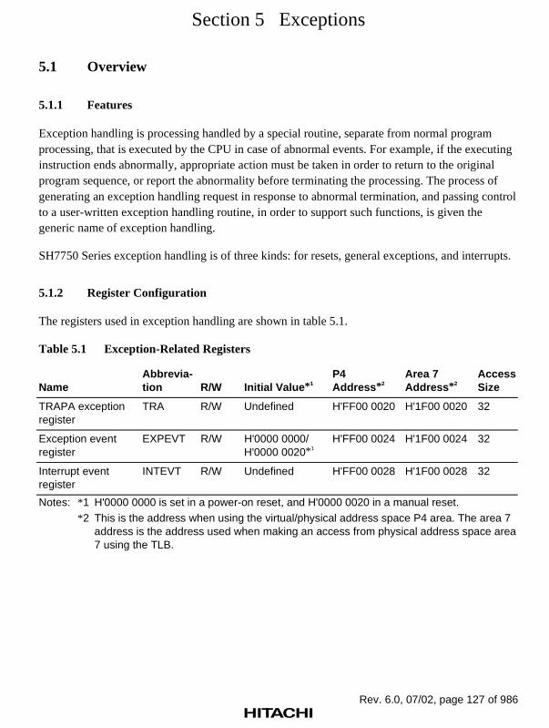
Rev. 6.0, 07/02, page 127 of 986
Section 5 Exceptions
5.1 Overview
5.1.1 Features
Exception handling is processing handled by a special routine, separate from normal programprocessing, that is executed by the CPU in case of abnormal events. For example, if the executinginstruction ends abnormally, appropriate action must be taken in order to return to the originalprogram sequence, or report the abnormality before terminating the processing. The process ofgenerating an exception handling request in response to abnormal termination, and passing controlto a user-written exception handling routine, in order to support such functions, is given thegeneric name of exception handling.
SH7750 Series exception handling is of three kinds: for resets, general exceptions, and interrupts.
5.1.2 Register Configuration
The registers used in exception handling are shown in table 5.1.
Table 5.1 Exception-Related Registers
NameAbbrevia-tion R/W Initial Value*1
P4Address*2
Area 7Address*2
AccessSize
TRAPA exceptionregister
TRA R/W Undefined H'FF00 0020 H'1F00 0020 32
Exception eventregister
EXPEVT R/W H'0000 0000/H'0000 0020*1
H'FF00 0024 H'1F00 0024 32
Interrupt eventregister
INTEVT R/W Undefined H'FF00 0028 H'1F00 0028 32
Notes: *1 H'0000 0000 is set in a power-on reset, and H'0000 0020 in a manual reset.*2 This is the address when using the virtual/physical address space P4 area. The area 7
address is the address used when making an access from physical address space area7 using the TLB.

Rev. 6.0, 07/02, page 128 of 986
5.2 Register Descriptions
There are three registers related to exception handling. Addresses are allocated to these registers,and they can be accessed by specifying the P4 address or area 7 address.
1. The exception event register (EXPEVT) resides at P4 address H'FF00 0024, and contains a 12-bit exception code. The exception code set in EXPEVT is that for a reset or general exceptionevent. The exception code is set automatically by hardware when an exception occurs.EXPEVT can also be modified by software.
2. The interrupt event register (INTEVT) resides at P4 address H'FF00 0028, and contains a 12-bit exception code. The exception code set in INTEVT is that for an interrupt request. Theexception code is set automatically by hardware when an exception occurs. INTEVT can alsobe modified by software.
3. The TRAPA exception register (TRA) resides at P4 address H'FF00 0020, and contains 8-bitimmediate data (imm) for the TRAPA instruction. TRA is set automatically by hardware whena TRAPA instruction is executed. TRA can also be modified by software.
The bit configurations of EXPEVT, INTEVT, and TRA are shown in figure 5.1.
31 0
0
0 0 0 0
0
31 10 9 1 0
0:
imm:
Reserved bits. These bits are always read as 0, and should only be written with 0.8-bit immediate data of the TRAPA instruction
12 11
2
EXPEVT and INTEVT
TRA
imm
Exception code
Figure 5.1 Register Bit Configurations
Rev. 6.0, 07/02, page 129 of 986
5.3 Exception Handling Functions
5.3.1 Exception Handling Flow
In exception handling, the contents of the program counter (PC), status register (SR), and R15 aresaved in the saved program counter (SPC), saved status register (SSR), and saved generalregister15(SGR), and the CPU starts execution of the appropriate exception handling routineaccording to the vector address. An exception handling routine is a program written by the user tohandle a specific exception. The exception handling routine is terminated and control returned tothe original program by executing a return-from-exception instruction (RTE). This instructionrestores the PC and SR contents and returns control to the normal processing routine at the point atwhich the exception occurred.
The SGR contents are not written back to R15 by an RTE instruction.
The basic processing flow is as follows. See section 2, Data Formats and Registers, for themeaning of the individual SR bits.
1. The PC, SR, and R15 contents are saved in SPC, SSR, and SGR.
2. The block bit (BL) in SR is set to 1.
3. The mode bit (MD) in SR is set to 1.
4. The register bank bit (RB) in SR is set to 1.
5. In a reset, the FPU disable bit (FD) in SR is cleared to 0.
6. The exception code is written to bits 11–0 of the exception event register (EXPEVT) orinterrupt event register (INTEVT).
7. The CPU branches to the determined exception handling vector address, and the exceptionhandling routine begins.
5.3.2 Exception Handling Vector Addresses
The reset vector address is fixed at H'A000 0000. Exception and interrupt vector addresses aredetermined by adding the offset for the specific event to the vector base address, which is set bysoftware in the vector base register (VBR). In the case of the TLB miss exception, for example,the offset is H'0000 0400, so if H'9C08 0000 is set in VBR, the exception handling vector addresswill be H'9C08 0400. If a further exception occurs at the exception handling vector address, aduplicate exception will result, and recovery will be difficult; therefore, fixed physical addresses(P1, P2) should be specified for vector addresses.
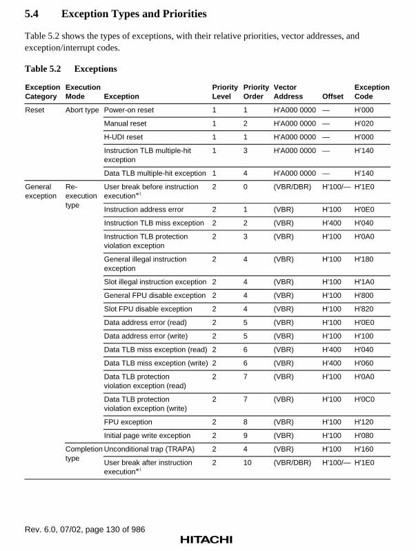
Rev. 6.0, 07/02, page 130 of 986
5.4 Exception Types and Priorities
Table 5.2 shows the types of exceptions, with their relative priorities, vector addresses, andexception/interrupt codes.
Table 5.2 Exceptions
ExceptionCategory
ExecutionMode Exception
PriorityLevel
PriorityOrder
VectorAddress Offset
ExceptionCode
Power-on reset 1 1 H'A000 0000 — H’000
Manual reset 1 2 H'A000 0000 — H’020
H-UDI reset 1 1 H'A000 0000 — H’000
Instruction TLB multiple-hitexception
1 3 H'A000 0000 — H’140
Reset Abort type
Data TLB multiple-hit exception 1 4 H'A000 0000 — H’140
User break before instructionexecution*1
2 0 (VBR/DBR) H'100/— H'1E0
Instruction address error 2 1 (VBR) H'100 H'0E0
Instruction TLB miss exception 2 2 (VBR) H'400 H'040
Instruction TLB protectionviolation exception
2 3 (VBR) H'100 H'0A0
General illegal instructionexception
2 4 (VBR) H'100 H'180
Slot illegal instruction exception 2 4 (VBR) H'100 H'1A0
General FPU disable exception 2 4 (VBR) H'100 H'800
Slot FPU disable exception 2 4 (VBR) H'100 H'820
Data address error (read) 2 5 (VBR) H'100 H'0E0
Data address error (write) 2 5 (VBR) H'100 H'100
Data TLB miss exception (read) 2 6 (VBR) H'400 H'040
Data TLB miss exception (write) 2 6 (VBR) H'400 H'060
Data TLB protectionviolation exception (read)
2 7 (VBR) H'100 H'0A0
Data TLB protectionviolation exception (write)
2 7 (VBR) H'100 H'0C0
FPU exception 2 8 (VBR) H'100 H'120
Re-executiontype
Initial page write exception 2 9 (VBR) H'100 H'080
Unconditional trap (TRAPA) 2 4 (VBR) H'100 H'160
Generalexception
Completiontype
User break after instructionexecution*1
2 10 (VBR/DBR) H'100/— H'1E0

Rev. 6.0, 07/02, page 131 of 986
Table 5.2 Exceptions (cont)
ExceptionCategory
ExecutionMode Exception
PriorityLevel
PriorityOrder
VectorAddress Offset
ExceptionCode
Nonmaskable interrupt 3 — (VBR) H'600 H'1C0
0 H'200
1 H'220
2 H'240
3 H'260
4 H'280
5 H'2A0
6 H'2C0
7 H'2E0
8 H'300
9 H'320
A H'340
B H'360
C H'380
D H'3A0
Externalinterrupts
IRL3–IRL0
E
4 *2 (VBR) H'600
H'3C0
TMU0 TUNI0 H'400
TMU1 TUNI1 H'420
TUNI2 H'440TMU2
TICPI2 H'460
TMU3 TUNI3 H'B00
TMU4 TUNI4 H'B80
ATI H'480
PRI H'4A0
RTC
CUI H'4C0
SCI ERI H'4E0
RXI H'500
TXI H'520
TEI H'540
WDT ITI H'560
RCMI H'580REF
ROVI
4 *2 (VBR) H'600
H'5A0
Interrupt Completiontype
Peripheralmoduleinterrupt(module/source)
H-UDI H-UDI H'600
GPIO GPIOI H'620

Rev. 6.0, 07/02, page 132 of 986
Table 5.2 Exceptions (cont)
ExceptionCategory
ExecutionMode Exception
PriorityLevel
PriorityOrder
VectorAddress Offset
ExceptionCode
DMTE0 H'640
DMTE1 H'660
DMTE2 H'680
DMTE3 H'6A0
DMTE4*3
H'780
DMTE5*3
H'7A0
DMTE6*3
H'7C0
DMTE7*3
H'7E0
DMAC
DMAE H'6C0
ERI H'700
RXI H'720
BRI H'740
Interrupt Completiontype
Peripheralmoduleinterrupt(module/source)
SCIF
TXI
4 *2 (VBR) H'600
H'760
Priority: Priority is first assigned by priority level, then by priority order within each level (the lowestnumber represents the highest priority).Exception transition destination: Control passes to H'A000 0000 in a reset, and to [VBR + offset] inother cases.Exception code: Stored in EXPEVT for a reset or general exception, and in INTEVT for an interrupt.IRL: Interrupt request level (pins IRL3–IRL0).
Module/source: See the sections on the relevant peripheral modules.
Notes: *1 When BRCR.UBDE = 1, PC = DBR. In other cases, PC = VBR + H'100.*2 The priority order of external interrupts and peripheral module interrupts can be set by
software.*3 SH7750R only.
5.5 Exception Flow
5.5.1 Exception Flow
Figure 5.2 shows an outline flowchart of the basic operations in instruction execution andexception handling. For the sake of clarity, the following description assumes that instructions areexecuted sequentially, one by one. Figure 5.2 shows the relative priority order of the differentkinds of exceptions (reset/general exception/interrupt). Register settings in the event of an

Rev. 6.0, 07/02, page 133 of 986
exception are shown only for SSR, SPC, SGR, EXPEVT/INTEVT, SR, and PC, but other registersmay be set automatically by hardware, depending on the exception. For details, see section 5.6,Description of Exceptions. Also, see section 5.6.4, Priority Order with Multiple Exceptions, forexception handling during execution of a delayed branch instruction and a delay slot instruction,and in the case of instructions in which two data accesses are performed.
Execute next instruction
Is highest- priority exception
re-exceptiontype?
Cancel instruction executionresult
Yes
Yes
Yes
No
No
No
No
Yes
SSR ← SRSPC ← PCSGR ← R15EXPEVT/INTEVT ← exception codeSR.MD,RB,BL ← 111PC ← (BRCR.UBDE=1 && User_Break?
DBR: (VBR + Offset))
EXPEVT ← exception codeSR. MD, RB, BL, FD, IMASK ← 11101111PC ← H'A000 0000
Interruptrequested?
Generalexception requested?
Resetrequested?
Figure 5.2 Instruction Execution and Exception Handling
5.5.2 Exception Source Acceptance
A priority ranking is provided for all exceptions for use in determining which of two or moresimultaneously generated exceptions should be accepted. Five of the general exceptions—thegeneral illegal instruction exception, slot illegal instruction exception, general FPU disableexception, slot FPU disable exception, and unconditional trap exception—are detected in theprocess of instruction decoding, and do not occur simultaneously in the instruction pipeline. Theseexceptions therefore all have the same priority. General exceptions are detected in the order ofinstruction execution. However, exception handling is performed in the order of instruction flow(program order). Thus, an exception for an earlier instruction is accepted before that for a laterinstruction. An example of the order of acceptance for general exceptions is shown in figure 5.3.
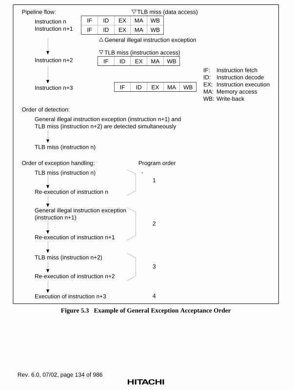
Rev. 6.0, 07/02, page 134 of 986
IF
IF
ID
ID
EX
EX
MA
MA
WB
WB
TLB miss (data access)Pipeline flow:
Order of detection:
Instruction nInstruction n+1
General illegal instruction exception (instruction n+1) and TLB miss (instruction n+2) are detected simultaneously
Order of exception handling:
TLB miss (instruction n)
Program order
1
Instruction n+2
General illegal instruction exception
IF ID EX MA WB
IF ID EX MA WB
TLB miss (instruction access)
2
3
4
IF: Instruction fetchID: Instruction decodeEX: Instruction executionMA: Memory accessWB: Write-back
Instruction n+3
TLB miss (instruction n)
Re-execution of instruction n
General illegal instruction exception (instruction n+1)
Re-execution of instruction n+1
TLB miss (instruction n+2)
Re-execution of instruction n+2
Execution of instruction n+3
Figure 5.3 Example of General Exception Acceptance Order

Rev. 6.0, 07/02, page 135 of 986
5.5.3 Exception Requests and BL Bit
When the BL bit in SR is 0, exceptions and interrupts are accepted.
When the BL bit in SR is 1 and an exception other than a user break is generated, the CPU'sinternal registers and the registers of the other modules are set to their states following a manualreset, and the CPU branches to the same address as in a reset (H'A000 0000). For the operation inthe event of a user break, see section 20, User Break Controller. If an ordinary interrupt occurs, theinterrupt request is held pending and is accepted after the BL bit has been cleared to 0 by software.If a nonmaskable interrupt (NMI) occurs, it can be held pending or accepted according to thesetting made by software.
Thus, normally, SPC and SSR are saved and then the BL bit in SR is cleared to 0, to enablemultiple exception state acceptance.
5.5.4 Return from Exception Handling
The RTE instruction is used to return from exception handling. When the RTE instruction isexecuted, the SPC contents are restored to PC and the SSR contents to SR, and the CPU returnsfrom the exception handling routine by branching to the SPC address. If SPC and SSR were savedto external memory, set the BL bit in SR to 1 before restoring the SPC and SSR contents andissuing the RTE instruction.
5.6 Description of Exceptions
The various exception handling operations are described here, covering exception sources,transition addresses, and processor operation when a transition is made.

Rev. 6.0, 07/02, page 136 of 986
5.6.1 Resets
(1) Power-On Reset
• Sources:
SCK2 pin high level and RESET pin low level
When the watchdog timer overflows while the WT/IT bit is set to 1 and the RSTS bit iscleared to 0 in WTCSR. For details, see section 10, Clock Oscillation Circuits.
• Transition address: H'A000 0000
• Transition operations:
Exception code H'000 is set in EXPEVT, initialization of VBR and SR is performed, and abranch is made to PC = H'A000 0000.
In the initialization processing, the VBR register is set to H'0000 0000, and in SR, the MD,RB, and BL bits are set to 1, the FD bit is cleared to 0, and the interrupt mask bits (I3–I0) areset to B'1111.
CPU and on-chip peripheral module initialization is performed. For details, see the registerdescriptions in the relevant sections. For some CPU functions, the TRST pin and RESET pinmust be driven low. It is therefore essential to execute a power-on reset and drive the TRSTpin low when powering on.
If the SCK2 pin is changed to the low level while the RESET pin is low, a manual reset mayoccur after the power-on reset operation. Do not drive the SCK2 pin low during this interval(see figure 22.3).
Power_on_reset()
EXPEVT = H'00000000;
VBR = H'00000000;
SR.MD = 1;
SR.RB = 1;
SR.BL = 1;
SR.(I0-I3) = B'1111;
SR.FD=0;
Initialize_CPU();
Initialize_Module(PowerOn);
PC = H'A0000000;

Rev. 6.0, 07/02, page 137 of 986
(2) Manual Reset
• Sources:
SCK2 pin low level and RESET pin low level
When a general exception other than a user break occurs while the BL bit is set to 1 in SR
When the watchdog timer overflows while the WT/IT bit and RSTS bit are both set to 1 inWTCSR. For details, see section 10, Clock Oscillation Circuits.
• Transition address: H'A000 0000
• Transition operations:
Exception code H'020 is set in EXPEVT, initialization of VBR and SR is performed, and abranch is made to PC = H'A000 0000.
In the initialization processing, the VBR register is set to H'0000 0000, and in SR, the MD,RB, and BL bits are set to 1, the FD bit is cleared to 0, and the interrupt mask bits (I3–I0) areset to B'1111.
CPU and on-chip peripheral module initialization is performed. For details, see the registerdescriptions in the relevant sections.
Manual_reset()
EXPEVT = H'00000020;
VBR = H'00000000;
SR.MD = 1;
SR.RB = 1;
SR.BL = 1;
SR.(I0-I3) = B'1111;
SR.FD = 0;
Initialize_CPU();
Initialize_Module(Manual);
PC = H'A0000000;
Table 5.3 Types of Reset
Reset State TransitionConditions Internal States
Type SCK2 RESETRESETRESETRESET CPUOn-Chip PeripheralModules
Power-on reset High Low Initialized
Manual reset Low Low Initialized
See RegisterConfiguration ineach section

Rev. 6.0, 07/02, page 138 of 986
(3) H-UDI Reset
• Source: SDIR.TI3–TI0 = B'0110 (negation) or B'0111 (assertion)
• Transition address: H'A000 0000
• Transition operations:
Exception code H'000 is set in EXPEVT, initialization of VBR and SR is performed, and abranch is made to PC = H'A000 0000.
In the initialization processing, the VBR register is set to H'0000 0000, and in SR, the MD,RB, and BL bits are set to 1, the FD bit is cleared to 0, and the interrupt mask bits (I3–I0) areset to B'1111.
CPU and on-chip peripheral module initialization is performed. For details, see the registerdescriptions in the relevant sections.
H-UDI_reset()
EXPEVT = H'00000000;
VBR = H'00000000;
SR.MD = 1;
SR.RB = 1;
SR.BL = 1;
SR.(I0-I3) = B'1111;
SR.FD = 0;
Initialize_CPU();
Initialize_Module(PowerOn);
PC = H'A0000000;

Rev. 6.0, 07/02, page 139 of 986
(4) Instruction TLB Multiple-Hit Exception
• Source: Multiple ITLB address matches
• Transition address: H'A000 0000
• Transition operations:
The virtual address (32 bits) at which this exception occurred is set in TEA, and thecorresponding virtual page number (22 bits) is set in PTEH [31:10]. ASID in PTEH indicatesthe ASID when this exception occurred.
Exception code H'140 is set in EXPEVT, initialization of VBR and SR is performed, and abranch is made to PC = H'A000 0000.
In the initialization processing, the VBR register is set to H'0000 0000, and in SR, the MD,RB, and BL bits are set to 1, the FD bit is cleared to 0, and the interrupt mask bits (I3–I0) areset to B'1111.
CPU and on-chip peripheral module initialization is performed in the same way as in a manualreset. For details, see the register descriptions in the relevant sections.
TLB_multi_hit()
TEA = EXCEPTION_ADDRESS;
PTEH.VPN = PAGE_NUMBER;
EXPEVT = H'00000140;
VBR = H'00000000;
SR.MD = 1;
SR.RB = 1;
SR.BL = 1;
SR.(I0-I3) = B'1111;
SR.FD = 0;
Initialize_CPU();
Initialize_Module(Manual);
PC = H'A0000000;

Rev. 6.0, 07/02, page 140 of 986
(5) Operand TLB Multiple-Hit Exception
• Source: Multiple UTLB address matches
• Transition address: H'A000 0000
• Transition operations:
The virtual address (32 bits) at which this exception occurred is set in TEA, and thecorresponding virtual page number (22 bits) is set in PTEH [31:10]. ASID in PTEH indicatesthe ASID when this exception occurred.
Exception code H'140 is set in EXPEVT, initialization of VBR and SR is performed, and abranch is made to PC = H'A000 0000.
In the initialization processing, the VBR register is set to H'0000 0000, and in SR, the MD,RB, and BL bits are set to 1, the FD bit is cleared to 0, and the interrupt mask bits (I3–I0) areset to B'1111.
CPU and on-chip peripheral module initialization is performed in the same way as in a manualreset. For details, see the register descriptions in the relevant sections.
TLB_multi_hit()
TEA = EXCEPTION_ADDRESS;
PTEH.VPN = PAGE_NUMBER;
EXPEVT = H'00000140;
VBR = H'00000000;
SR.MD = 1;
SR.RB = 1;
SR.BL = 1;
SR.(I0-I3) = B'1111;
SR.FD = 0;
Initialize_CPU();
Initialize_Module(Manual);
PC = H'A0000000;

Rev. 6.0, 07/02, page 141 of 986
5.6.2 General Exceptions
(1) Data TLB Miss Exception
• Source: Address mismatch in UTLB address comparison
• Transition address: VBR + H'0000 0400
• Transition operations:
The virtual address (32 bits) at which this exception occurred is set in TEA, and thecorresponding virtual page number (22 bits) is set in PTEH [31:10]. ASID in PTEH indicatesthe ASID when this exception occurred.
The PC and SR contents for the instruction at which this exception occurred are saved in SPCand SSR, and the contents of R15 are saved in SGR.
Exception code H'040 (for a read access) or H'060 (for a write access) is set in EXPEVT. TheBL, MD, and RB bits are set to 1 in SR, and a branch is made to PC = VBR + H'0400.
To speed up TLB miss processing, the offset is separate from that of other exceptions.
Data_TLB_miss_exception()
TEA = EXCEPTION_ADDRESS;
PTEH.VPN = PAGE_NUMBER;
SPC = PC;
SSR = SR;
SGR = R15;
EXPEVT = read_access ? H'00000040 : H'00000060;
SR.MD = 1;
SR.RB = 1;
SR.BL = 1;
PC = VBR + H'00000400;

Rev. 6.0, 07/02, page 142 of 986
(2) Instruction TLB Miss Exception
• Source: Address mismatch in ITLB address comparison
• Transition address: VBR + H'0000 0400
• Transition operations:
The virtual address (32 bits) at which this exception occurred is set in TEA, and thecorresponding virtual page number (22 bits) is set in PTEH [31:10]. ASID in PTEH indicatesthe ASID when this exception occurred.
The PC and SR contents for the instruction at which this exception occurred are saved in SPCand SSR, and the contents of R15 are saved in SGR.
Exception code H'040 is set in EXPEVT. The BL, MD, and RB bits are set to 1 in SR, and abranch is made to PC = VBR + H'0400.
To speed up TLB miss processing, the offset is separate from that of other exceptions.
ITLB_miss_exception()
TEA = EXCEPTION_ADDRESS;
PTEH.VPN = PAGE_NUMBER;
SPC = PC;
SSR = SR;
SGR = R15;
EXPEVT = H'00000040;
SR.MD = 1;
SR.RB = 1;
SR.BL = 1;
PC = VBR + H'00000400;

Rev. 6.0, 07/02, page 143 of 986
(3) Initial Page Write Exception
• Source: TLB is hit in a store access, but dirty bit D = 0
• Transition address: VBR + H'0000 0100
• Transition operations:
The virtual address (32 bits) at which this exception occurred is set in TEA, and thecorresponding virtual page number (22 bits) is set in PTEH [31:10]. ASID in PTEH indicatesthe ASID when this exception occurred.
The PC and SR contents for the instruction at which this exception occurred are saved in SPCand SSR, and the contents of R15 are saved in SGR.
Exception code H'080 is set in EXPEVT. The BL, MD, and RB bits are set to 1 in SR, and abranch is made to PC = VBR + H'0100.
Initial_write_exception()
TEA = EXCEPTION_ADDRESS;
PTEH.VPN = PAGE_NUMBER;
SPC = PC;
SSR = SR;
SGR = R15;
EXPEVT = H'00000080;
SR.MD = 1;
SR.RB = 1;
SR.BL = 1;
PC = VBR + H'00000100;

Rev. 6.0, 07/02, page 144 of 986
(4) Data TLB Protection Violation Exception
• Source: The access does not accord with the UTLB protection information (PR bits) shownbelow.
PR Privileged Mode User Mode
00 Only read access possible Access not possible
01 Read/write access possible Access not possible
10 Only read access possible Only read access possible
11 Read/write access possible Read/write access possible
• Transition address: VBR + H'0000 0100
• Transition operations:
The virtual address (32 bits) at which this exception occurred is set in TEA, and thecorresponding virtual page number (22 bits) is set in PTEH [31:10]. ASID in PTEH indicatesthe ASID when this exception occurred.
The PC and SR contents for the instruction at which this exception occurred are saved in SPCand SSR, and the contents of R15 are saved in SGR.
Exception code H'0A0 (for a read access) or H'0C0 (for a write access) is set in EXPEVT. TheBL, MD, and RB bits are set to 1 in SR, and a branch is made to PC = VBR + H'0100.
Data_TLB_protection_violation_exception()
TEA = EXCEPTION_ADDRESS;
PTEH.VPN = PAGE_NUMBER;
SPC = PC;
SSR = SR;
SGR = R15;
EXPEVT = read_access ? H'000000A0 : H'000000C0;
SR.MD = 1;
SR.RB = 1;
SR.BL = 1;
PC = VBR + H'00000100;

Rev. 6.0, 07/02, page 145 of 986
(5) Instruction TLB Protection Violation Exception
• Source: The access does not accord with the ITLB protection information (PR bits) shownbelow.
PR Privileged Mode User Mode
0 Access possible Access not possible
1 Access possible Access possible
• Transition address: VBR + H'0000 0100
• Transition operations:
The virtual address (32 bits) at which this exception occurred is set in TEA, and thecorresponding virtual page number (22 bits) is set in PTEH [31:10]. ASID in PTEH indicatesthe ASID when this exception occurred.
The PC and SR contents for the instruction at which this exception occurred are saved in SPCand SSR, and the contents of R15 are saved in SGR.
Exception code H'0A0 is set in EXPEVT. The BL, MD, and RB bits are set to 1 in SR, and abranch is made to PC = VBR + H'0100.
ITLB_protection_violation_exception()
TEA = EXCEPTION_ADDRESS;
PTEH.VPN = PAGE_NUMBER;
SPC = PC;
SSR = SR;
SGR = R15;
EXPEVT = H'000000A0;
SR.MD = 1;
SR.RB = 1;
SR.BL = 1;
PC = VBR + H'00000100;

Rev. 6.0, 07/02, page 146 of 986
(6) Data Address Error
• Sources:
Word data access from other than a word boundary (2n +1)
Longword data access from other than a longword data boundary (4n +1, 4n + 2, or 4n +3)
Quadword data access from other than a quadword data boundary (8n +1, 8n + 2, 8n +3, 8n+ 4, 8n + 5, 8n + 6, or 8n + 7)
Access to area H'8000 0000–H'FFFF FFFF in user mode
• Transition address: VBR + H'0000 0100
• Transition operations:
The virtual address (32 bits) at which this exception occurred is set in TEA, and thecorresponding virtual page number (22 bits) is set in PTEH [31:10]. ASID in PTEH indicatesthe ASID when this exception occurred.
The PC and SR contents for the instruction at which this exception occurred are saved in SPCand SSR, and the contents of R15 are saved in SGR.
Exception code H'0E0 (for a read access) or H'100 (for a write access) is set in EXPEVT. TheBL, MD, and RB bits are set to 1 in SR, and a branch is made to PC = VBR + H'0100. Fordetails, see section 3, Memory Management Unit (MMU).
Data_address_error()
TEA = EXCEPTION_ADDRESS;
PTEN.VPN = PAGE_NUMBER;
SPC = PC;
SSR = SR;
SGR = R15;
EXPEVT = read_access? H'000000E0: H'00000100;
SR.MD = 1;
SR.RB = 1;
SR.BL = 1;
PC = VBR + H'00000100;

Rev. 6.0, 07/02, page 147 of 986
(7) Instruction Address Error
• Sources:
Instruction fetch from other than a word boundary (2n +1)
Instruction fetch from area H'8000 0000–H'FFFF FFFF in user mode
• Transition address: VBR + H'0000 0100
• Transition operations:
The virtual address (32 bits) at which this exception occurred is set in TEA, and thecorresponding virtual page number (22 bits) is set in PTEH [31:10]. ASID in PTEH indicatesthe ASID when this exception occurred.
The PC and SR contents for the instruction at which this exception occurred are saved in SPCand SSR, and the contents of R15 are saved in SGR.
Exception code H'0E0 is set in EXPEVT. The BL, MD, and RB bits are set to 1 in SR, and abranch is made to PC = VBR + H'0100. For details, see section 3, Memory Management Unit(MMU).
Instruction_address_error()
TEA = EXCEPTION_ADDRESS;
PTEN.VPN = PAGE_NUMBER;
SPC = PC;
SSR = SR;
SGR = R15;
EXPEVT = H'000000E0;
SR.MD = 1;
SR.RB = 1;
SR.BL = 1;
PC = VBR + H'00000100;
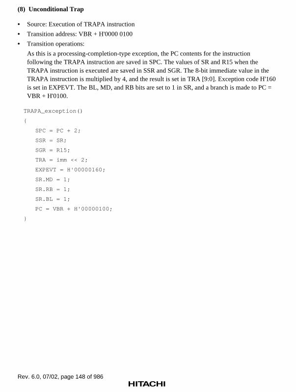
Rev. 6.0, 07/02, page 148 of 986
(8) Unconditional Trap
• Source: Execution of TRAPA instruction
• Transition address: VBR + H'0000 0100
• Transition operations:
As this is a processing-completion-type exception, the PC contents for the instructionfollowing the TRAPA instruction are saved in SPC. The values of SR and R15 when theTRAPA instruction is executed are saved in SSR and SGR. The 8-bit immediate value in theTRAPA instruction is multiplied by 4, and the result is set in TRA [9:0]. Exception code H'160is set in EXPEVT. The BL, MD, and RB bits are set to 1 in SR, and a branch is made to PC =VBR + H'0100.
TRAPA_exception()
SPC = PC + 2;
SSR = SR;
SGR = R15;
TRA = imm << 2;
EXPEVT = H'00000160;
SR.MD = 1;
SR.RB = 1;
SR.BL = 1;
PC = VBR + H'00000100;

Rev. 6.0, 07/02, page 149 of 986
(9) General Illegal Instruction Exception
• Sources:
Decoding of an undefined instruction not in a delay slot
Delayed branch instructions: JMP, JSR, BRA, BRAF, BSR, BSRF, RTS, RTE, BT/S, BF/S
Undefined instruction: H'FFFD
Decoding in user mode of a privileged instruction not in a delay slot
Privileged instructions: LDC, STC, RTE, LDTLB, SLEEP, but excluding LDC/STCinstructions that access GBR
• Transition address: VBR + H'0000 0100
• Transition operations:
The PC and SR contents for the instruction at which this exception occurred are saved in SPCand SSR, and the contents of R15 are saved in SGR.
Exception code H'180 is set in EXPEVT. The BL, MD, and RB bits are set to 1 in SR, and abranch is made to PC = VBR + H'0100. Operation is not guaranteed if an undefined code otherthan H'FFFD is decoded.
General_illegal_instruction_exception()
SPC = PC;
SSR = SR;
SGR = R15;
EXPEVT = H'00000180;
SR.MD = 1;
SR.RB = 1;
SR.BL = 1;
PC = VBR + H'00000100;

Rev. 6.0, 07/02, page 150 of 986
(10) Slot Illegal Instruction Exception
• Sources:
Decoding of an undefined instruction in a delay slot
Delayed branch instructions: JMP, JSR, BRA, BRAF, BSR, BSRF, RTS, RTE, BT/S, BF/S
Undefined instruction: H'FFFD
Decoding of an instruction that modifies PC in a delay slot
Instructions that modify PC: JMP, JSR, BRA, BRAF, BSR, BSRF, RTS, RTE, BT, BF,BT/S, BF/S, TRAPA, LDC Rm, SR, LDC.L @Rm+, SR
Decoding in user mode of a privileged instruction in a delay slot
Privileged instructions: LDC, STC, RTE, LDTLB, SLEEP, but excluding LDC/STCinstructions that access GBR
Decoding of a PC-relative MOV instruction or MOVA instruction in a delay slot
• Transition address: VBR + H'0000 0100
• Transition operations:
The PC contents for the preceding delayed branch instruction are saved in SPC. The SR andR15 contents when this exception occurred are saved in SSR and SGR.
Exception code H'1A0 is set in EXPEVT. The BL, MD, and RB bits are set to 1 in SR, and abranch is made to PC = VBR + H'0100. Operation is not guaranteed if an undefined code otherthan H'FFFD is decoded.
Slot_illegal_instruction_exception()
SPC = PC - 2;
SSR = SR;
SGR = R15;
EXPEVT = H'000001A0;
SR.MD = 1;
SR.RB = 1;
SR.BL = 1;
PC = VBR + H'00000100;

Rev. 6.0, 07/02, page 151 of 986
(11) General FPU Disable Exception
• Source: Decoding of an FPU instruction* not in a delay slot with SR.FD =1
• Transition address: VBR + H'0000 0100
• Transition operations:
The PC and SR contents for the instruction at which this exception occurred are saved in SPCand SSR, and the contents of R15 are saved in SGR.
Exception code H'800 is set in EXPEVT. The BL, MD, and RB bits are set to 1 in SR, and abranch is made to PC = VBR + H'0100.
Note: * FPU instructions are instructions in which the first 4 bits of the instruction code are F (butexcluding undefined instruction H'FFFD), and the LDS, STS, LDS.L, and STS.Linstructions corresponding to FPUL and FPSCR.
General_fpu_disable_exception()
SPC = PC;
SSR = SR;
SGR = R15;
EXPEVT = H'00000800;
SR.MD = 1;
SR.RB = 1;
SR.BL = 1;
PC = VBR + H'00000100;

Rev. 6.0, 07/02, page 152 of 986
(12) Slot FPU Disable Exception
• Source: Decoding of an FPU instruction in a delay slot with SR.FD =1
• Transition address: VBR + H'0000 0100
• Transition operations:
The PC contents for the preceding delayed branch instruction are saved in SPC. The SR andR15 contents when this exception occurred are saved in SSR and SGR.
Exception code H'820 is set in EXPEVT. The BL, MD, and RB bits are set to 1 in SR, and abranch is made to PC = VBR + H'0100.
Slot_fpu_disable_exception()
SPC = PC - 2;
SSR = SR;
SGR = R15;
EXPEVT = H'00000820;
SR.MD = 1;
SR.RB = 1;
SR.BL = 1;
PC = VBR + H'00000100;

Rev. 6.0, 07/02, page 153 of 986
(13) User Breakpoint Trap
• Source: Fulfilling of a break condition set in the user break controller
• Transition address: VBR + H'0000 0100, or DBR
• Transition operations:
In the case of a post-execution break, the PC contents for the instruction following theinstruction at which the breakpoint is set are set in SPC. In the case of a pre-execution break,the PC contents for the instruction at which the breakpoint is set are set in SPC.
The SR and R15 contents when the break occurred are saved in SSR and SGR. Exception codeH'1E0 is set in EXPEVT.
The BL, MD, and RB bits are set to 1 in SR, and a branch is made to PC = VBR + H'0100. It isalso possible to branch to PC = DBR.
For details of PC, etc., when a data break is set, see section 20, User Break Controller (UBC).
User_break_exception()
SPC = (pre_execution break? PC : PC + 2);
SSR = SR;
SGR = R15;
EXPEVT = H'000001E0;
SR.MD = 1;
SR.RB = 1;
SR.BL = 1;
PC = (BRCR.UBDE==1 ? DBR : VBR + H’00000100);

Rev. 6.0, 07/02, page 154 of 986
(14) FPU Exception
• Source: Exception due to execution of a floating-point operation
• Transition address: VBR + H'0000 0100
• Transition operations:
The PC and SR contents for the instruction at which this exception occurred are saved in SPCand SSR, and the contents of R15 are saved in SGR. Exception code H'120 is set in EXPEVT.The BL, MD, and RB bits are set to 1 in SR, and a branch is made to PC = VBR + H'0100.
FPU_exception()
SPC = PC;
SSR = SR;
SGR = R15;
EXPEVT = H'00000120;
SR.MD = 1;
SR.RB = 1;
SR.BL = 1;
PC = VBR + H'00000100;

Rev. 6.0, 07/02, page 155 of 986
5.6.3 Interrupts
(1) NMI
• Source: NMI pin edge detection
• Transition address: VBR + H'0000 0600
• Transition operations:
The contents of PC and SR immediately after the instruction at which this interrupt wasaccepted are saved in SPC and SSR, and the contents of R15 are saved in SGR.
Exception code H'1C0 is set in INTEVT. The BL, MD, and RB bits are set to 1 in SR, and abranch is made to PC = VBR + H'0600. When the BL bit in SR is 0, this interrupt is notmasked by the interrupt mask bits in SR, and is accepted at the highest priority level. When theBL bit in SR is 1, a software setting can specify whether this interrupt is to be masked oraccepted. For details, see section 19, Interrupt Controller (INTC).
NMI()
SPC = PC;
SSR = SR;
SGR = R15;
INTEVT = H'000001C0;
SR.MD = 1;
SR.RB = 1;
SR.BL = 1;
PC = VBR + H'00000600;

Rev. 6.0, 07/02, page 156 of 986
(2) IRL Interrupts
• Source: The interrupt mask bit setting in SR is smaller than the IRL (3–0) level, and the BL bitin SR is 0 (accepted at instruction boundary).
• Transition address: VBR + H'0000 0600
• Transition operations:
The PC contents immediately after the instruction at which the interrupt is accepted are set inSPC. The SR and R15 contents at the time of acceptance are set in SSR and SGR.
The code corresponding to the IRL (3–0) level is set in INTEVT. See table 19.5, InterruptException Handling Sources and Priority Order, for the corresponding codes. The BL, MD,and RB bits are set to 1 in SR, and a branch is made to VBR + H'0600. The acceptance level isnot set in the interrupt mask bits in SR. When the BL bit in SR is 1, the interrupt is masked.For details, see section 19, Interrupt Controller (INTC).
IRL()
SPC = PC;
SSR = SR;
SGR = R15;
INTEVT = H'00000200 ~ H'000003C0;
SR.MD = 1;
SR.RB = 1;
SR.BL = 1;
PC = VBR + H'00000600;

Rev. 6.0, 07/02, page 157 of 986
(3) Peripheral Module Interrupts
• Source: The interrupt mask bit setting in SR is smaller than the peripheral module (H-UDI,GPIO, DMAC, TMU, RTC, SCI, SCIF, WDT, or REF) interrupt level, and the BL bit in SR is0 (accepted at instruction boundary).
• Transition address: VBR + H'0000 0600
• Transition operations:
The PC contents immediately after the instruction at which the interrupt is accepted are set inSPC. The SR and R15 contents at the time of acceptance are set in SSR and SGR.
The code corresponding to the interrupt source is set in INTEVT. The BL, MD, and RB bitsare set to 1 in SR, and a branch is made to VBR + H'0600. The module interrupt levels shouldbe set as values between B'0000 and B'1111 in the interrupt priority registers (IPRA–IPRC) inthe interrupt controller. For details, see section 19, Interrupt Controller (INTC).
Module_interruption()
SPC = PC;
SSR = SR;
SGR = R15;
INTEVT = H'00000400 ~ H'B80;
SR.MD = 1;
SR.RB = 1;
SR.BL = 1;
PC = VBR + H'00000600;

Rev. 6.0, 07/02, page 158 of 986
5.6.4 Priority Order with Multiple Exceptions
With some instructions, such as instructions that make two accesses to memory, and theindivisible pair comprising a delayed branch instruction and delay slot instruction, multipleexceptions occur. Care is required in these cases, as the exception priority order differs from thenormal order.
1. Instructions that make two accesses to memory
With MAC instructions, memory-to-memory arithmetic/logic instructions, and TASinstructions, two data transfers are performed by a single instruction, and an exception will bedetected for each of these data transfers. In these cases, therefore, the following order is usedto determine priority.
a. Data address error in first data transfer
b. TLB miss in first data transfer
c. TLB protection violation in first data transfer
d. Initial page write exception in first data transfer
e. Data address error in second data transfer
f. TLB miss in second data transfer
g. TLB protection violation in second data transfer
h. Initial page write exception in second data transfer
2. Indivisible delayed branch instruction and delay slot instruction
As a delayed branch instruction and its associated delay slot instruction are indivisible, theyare treated as a single instruction. Consequently, the priority order for exceptions that occur inthese instructions differs from the usual priority order. The priority order shown below is forthe case where the delay slot instruction has only one data transfer.
a. A check is performed for the interrupt type and reexecution type exceptions of prioritylevels 1 and 2 in the delayed branch instruction.
b. A check is performed for the interrupt type and reexecution type exceptions of prioritylevels 1 and 2 in the delay slot instruction.
c. A check is performed for the completion type exception of priority level 2 in the delayedbranch instruction.
d. A check is performed for the completion type exception of priority level 2 in the delay slotinstruction.
e. A check is performed for priority level 3 in the delayed branch instruction and prioritylevel 3 in the delay slot instruction. (There is no priority ranking between these two.)
f. A check is performed for priority level 4 in the delayed branch instruction and prioritylevel 4 in the delay slot instruction. (There is no priority ranking between these two.)
If the delay slot instruction has a second data transfer, two checks are performed in step b, as in1 above.

Rev. 6.0, 07/02, page 159 of 986
If the accepted exception (the highest-priority exception) is a delay slot instruction re-execution type exception, the branch instruction PR register write operation (PC → PRoperation performed in BSR, BSRF, JSR) is inhibited.
5.7 Usage Notes
1. Return from exception handling
a. Check the BL bit in SR with software. If SPC and SSR have been saved to externalmemory, set the BL bit in SR to 1 before restoring them.
b. Issue an RTE instruction. When RTE is executed, the SPC contents are set in PC, the SSRcontents are set in SR, and branch is made to the SPC address to return from the exceptionhandling routine.
2. If an exception or interrupt occurs when SR.BL = 1
a. Exception
When an exception other than a user break occurs, a manual reset is executed. The value inEXPEVT at this time is H'0000 0020; the value of the SPC and SSR registers is undefined.
b. Interrupt
If an ordinary interrupt occurs, the interrupt request is held pending and is accepted afterthe BL bit in SR has been cleared to 0 by software. If a nonmaskable interrupt (NMI)occurs, it can be held pending or accepted according to the setting made by software. In thesleep or standby state, however, an interrupt is accepted even if the BL bit in SR is set to 1.
3. SPC when an exception occurs
a. Re-execution type exception
The PC value for the instruction in which the exception occurred is set in SPC, and theinstruction is re-executed after returning from exception handling. If an exception occurs ina delay slot instruction, however, the PC value for the delay slot instruction is saved in SPCregardless of whether or not the preceding delay slot instruction condition is satisfied.
b. Completion type exception or interrupt
The PC value for the instruction following that in which the exception occurred is set inSPC. If an exception occurs in a branch instruction with delay slot, however, the PC valuefor the branch destination is saved in SPC.
4. An exception must not be generated in an RTE instruction delay slot, as the operation will beundefined in this case.

Rev. 6.0, 07/02, page 160 of 986
5.8 Restrictions
1. Restrictions on first instruction of exception handling routine
• Do not locate a BT, BF, BT/S, BF/S, BRA, or BSR instruction at address VBR + H'100, VBR+ H'400, or VBR + H'600.
• When the UBDE bit in the BRCR register is set to 1 and the user break debug supportfunction* is used, do not locate a BT, BF, BT/S, BF/S, BRA, or BSR instruction at the addressindicated by the DBR register.
Note: * See section 20.4, User Break Debug Support Function.

Rev. 6.0, 07/02, page 161 of 986
Section 6 Floating-Point Unit
6.1 Overview
The floating-point unit (FPU) has the following features:
• Conforms to IEEE754 standard
• 32 single-precision floating-point registers (can also be referenced as 16 double-precisionregisters)
• Two rounding modes: Round to Nearest and Round to Zero
• Two denormalization modes: Flush to Zero and Treat Denormalized Number
• Six exception sources: FPU Error, Invalid Operation, Divide By Zero, Overflow, Underflow,and Inexact
• Comprehensive instructions: Single-precision, double-precision, graphics support, systemcontrol
When the FD bit in SR is set to 1, the FPU cannot be used, and an attempt to execute an FPUinstruction will cause an FPU disable exception.
6.2 Data Formats
6.2.1 Floating-Point Format
A floating-point number consists of the following three fields:
• Sign (s)
• Exponent (e)
• Fraction (f)
The SH7750 Series can handle single-precision and double-precision floating-point numbers,using the formats shown in figures 6.1 and 6.2.
31
s e f
30 23 22 0
Figure 6.1 Format of Single-Precision Floating-Point Number

Rev. 6.0, 07/02, page 162 of 986
63
s e f
62 52 51 0
Figure 6.2 Format of Double-Precision Floating-Point Number
The exponent is expressed in biased form, as follows:
e = E + bias
The range of unbiased exponent E is Emin – 1 to Emax + 1. The two values Emin – 1 and Emax + 1 aredistinguished as follows. Emin – 1 indicates zero (both positive and negative sign) and adenormalized number, and Emax + 1 indicates positive or negative infinity or a non-number (NaN).Table 6.1 shows bias, Emin, and Emax values.
Table 6.1 Floating-Point Number Formats and Parameters
Parameter Single-Precision Double-Precision
Total bit width 32 bits 64 bits
Sign bit 1 bit 1 bit
Exponent field 8 bits 11 bits
Fraction field 23 bits 52 bits
Precision 24 bits 53 bits
Bias +127 +1023
Emax +127 +1023
Emin –126 –1022
Floating-point number value v is determined as follows:
If E = Emax + 1 and f ≠ 0, v is a non-number (NaN) irrespective of sign sIf E = Emax + 1 and f = 0, v = (–1)s (infinity) [positive or negative infinity]If Emin ≤ E ≤ Emax , v = (–1)s2E (1.f) [normalized number]If E = Emin – 1 and f ≠ 0, v = (–1)s2Emin (0.f) [denormalized number]If E = Emin – 1 and f = 0, v = (–1)s0 [positive or negative zero]
Table 6.2 shows the ranges of the various numbers in hexadecimal notation.

Rev. 6.0, 07/02, page 163 of 986
Table 6.2 Floating-Point Ranges
Type Single-Precision Double-Precision
Signaling non-number H'7FFFFFFF to H'7FC00000 H'7FFFFFFF FFFFFFFF toH'7FF80000 00000000
Quiet non-number H'7FBFFFFF to H'7F800001 H'7FF7FFFF FFFFFFFF toH'7FF00000 00000001
Positive infinity H'7F800000 H'7FF00000 00000
Positive normalizednumber
H'7F7FFFFF to H'00800000 H'7FEFFFFF FFFFFFFF toH'00100000 00000000
Positive denormalizednumber
H'007FFFFF to H'00000001 H'000FFFFF FFFFFFFF toH'00000000 00000001
Positive zero H'00000000 H'00000000 00000000
Negative zero H'80000000 H'80000000 00000000
Negative denormalizednumber
H'80000001 to H'807FFFFF H'80000000 00000001 toH'800FFFFF FFFFFFFF
Negative normalizednumber
H'80800000 to H'FF7FFFFF H'80100000 00000000 toH'FFEFFFFF FFFFFFFF
Negative infinity H'FF800000 H'FFF00000 00000000
Quiet non-number H'FF800001 to H'FFBFFFFF H'FFF00000 00000001 toH'FFF7FFFF FFFFFFFF
Signaling non-number H'FFC00000 to H'FFFFFFFF H'FFF80000 00000000 toH'FFFFFFFF FFFFFFFF
6.2.2 Non-Numbers (NaN)
Figure 6.3 shows the bit pattern of a non-number (NaN). A value is NaN in the following case:
• Sign bit: Don’t care
• Exponent field: All bits are 1
• Fraction field: At least one bit is 1
The NaN is a signaling NaN (sNaN) if the MSB of the fraction field is 1, and a quiet NaN (qNaN)if the MSB is 0.

Rev. 6.0, 07/02, page 164 of 986
31
x 11111111 Nxxxxxxxxxxxxxxxxxxxxxx
30 23 22 0
N = 1: sNaNN = 0: qNaN
Figure 6.3 Single-Precision NaN Bit Pattern
An sNaN is input in an operation, except copy, FABS, and FNEG, that generates a floating-pointvalue.
• When the EN.V bit in the FPSCR register is 0, the operation result (output) is a qNaN.
• When the EN.V bit in the FPSCR register is 1, an invalid operation exception will begenerated. In this case, the contents of the operation destination register are unchanged.
If a qNaN is input in an operation that generates a floating-point value, and an sNaN has not beeninput in that operation, the output will always be a qNaN irrespective of the setting of the EN.V bitin the FPSCR register. An exception will not be generated in this case.
The qNAN values generated by the SH7750 Series as operation results are as follows:
• Single-precision qNaN: H'7FBFFFFF
• Double-precision qNaN: H'7FF7FFFF FFFFFFFF
See the individual instruction descriptions for details of floating-point operations when a non-number (NaN) is input.
6.2.3 Denormalized Numbers
For a denormalized number floating-point value, the exponent field is expressed as 0, and thefraction field as a non-zero value.
When the DN bit in the FPU’s status register FPSCR is 1, a denormalized number (source operandor operation result) is always flushed to 0 in a floating-point operation that generates a value (anoperation other than copy, FNEG, or FABS).
When the DN bit in FPSCR is 0, a denormalized number (source operand or operation result) isprocessed as it is. See the individual instruction descriptions for details of floating-pointoperations when a denormalized number is input.
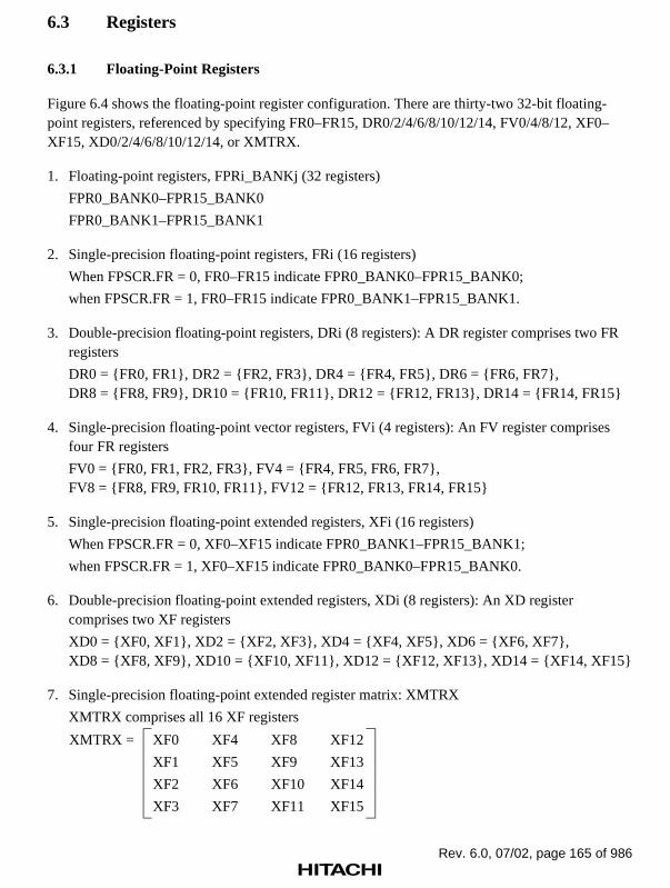
Rev. 6.0, 07/02, page 165 of 986
6.3 Registers
6.3.1 Floating-Point Registers
Figure 6.4 shows the floating-point register configuration. There are thirty-two 32-bit floating-point registers, referenced by specifying FR0–FR15, DR0/2/4/6/8/10/12/14, FV0/4/8/12, XF0–XF15, XD0/2/4/6/8/10/12/14, or XMTRX.
1. Floating-point registers, FPRi_BANKj (32 registers)
FPR0_BANK0–FPR15_BANK0
FPR0_BANK1–FPR15_BANK1
2. Single-precision floating-point registers, FRi (16 registers)
When FPSCR.FR = 0, FR0–FR15 indicate FPR0_BANK0–FPR15_BANK0;
when FPSCR.FR = 1, FR0–FR15 indicate FPR0_BANK1–FPR15_BANK1.
3. Double-precision floating-point registers, DRi (8 registers): A DR register comprises two FRregisters
DR0 = FR0, FR1, DR2 = FR2, FR3, DR4 = FR4, FR5, DR6 = FR6, FR7,DR8 = FR8, FR9, DR10 = FR10, FR11, DR12 = FR12, FR13, DR14 = FR14, FR15
4. Single-precision floating-point vector registers, FVi (4 registers): An FV register comprisesfour FR registers
FV0 = FR0, FR1, FR2, FR3, FV4 = FR4, FR5, FR6, FR7,FV8 = FR8, FR9, FR10, FR11, FV12 = FR12, FR13, FR14, FR15
5. Single-precision floating-point extended registers, XFi (16 registers)
When FPSCR.FR = 0, XF0–XF15 indicate FPR0_BANK1–FPR15_BANK1;
when FPSCR.FR = 1, XF0–XF15 indicate FPR0_BANK0–FPR15_BANK0.
6. Double-precision floating-point extended registers, XDi (8 registers): An XD registercomprises two XF registers
XD0 = XF0, XF1, XD2 = XF2, XF3, XD4 = XF4, XF5, XD6 = XF6, XF7,XD8 = XF8, XF9, XD10 = XF10, XF11, XD12 = XF12, XF13, XD14 = XF14, XF15
7. Single-precision floating-point extended register matrix: XMTRX
XMTRX comprises all 16 XF registers
XMTRX = XF0 XF4 XF8 XF12
XF1 XF5 XF9 XF13
XF2 XF6 XF10 XF14
XF3 XF7 XF11 XF15
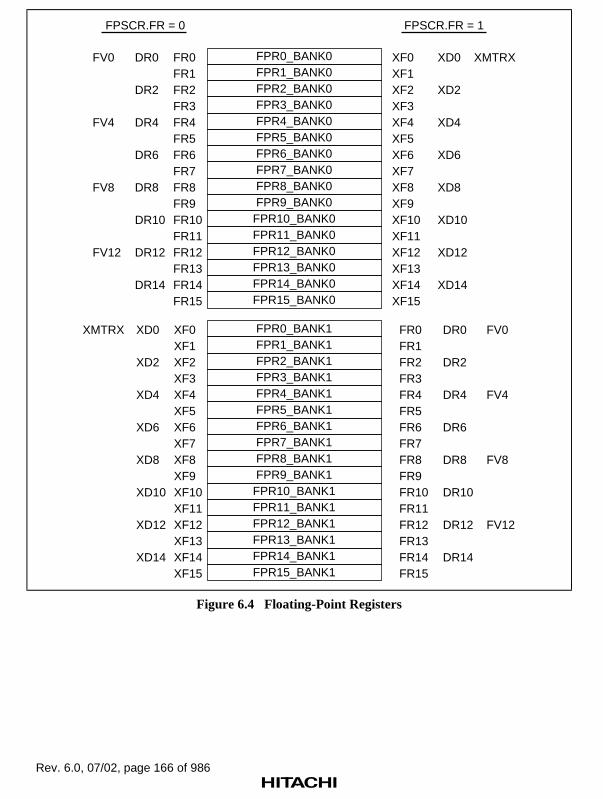
Rev. 6.0, 07/02, page 166 of 986
FPR0_BANK0FPR1_BANK0FPR2_BANK0FPR3_BANK0FPR4_BANK0FPR5_BANK0FPR6_BANK0FPR7_BANK0FPR8_BANK0FPR9_BANK0
FPR10_BANK0FPR11_BANK0FPR12_BANK0FPR13_BANK0FPR14_BANK0FPR15_BANK0
XF0XF1XF2 XF3XF4XF5XF6XF7 XF8 XF9 XF10 XF11XF12XF13XF14XF15
FR0FR1FR2 FR3FR4FR5FR6FR7 FR8 FR9 FR10 FR11FR12FR13FR14FR15
DR0
DR2
DR4
DR6
DR8
DR10
DR12
DR14
FV0
FV4
FV8
FV12
XD0 XMTRX
XD2
XD4
XD6
XD8
XD10
XD12
XD14
FPR0_BANK1FPR1_BANK1FPR2_BANK1FPR3_BANK1FPR4_BANK1FPR5_BANK1FPR6_BANK1FPR7_BANK1FPR8_BANK1FPR9_BANK1
FPR10_BANK1FPR11_BANK1FPR12_BANK1FPR13_BANK1FPR14_BANK1FPR15_BANK1
XF0XF1XF2 XF3XF4XF5XF6XF7 XF8 XF9 XF10 XF11XF12XF13XF14XF15
FR0FR1FR2 FR3FR4FR5FR6FR7 FR8 FR9 FR10 FR11FR12FR13FR14FR15
DR0
DR2
DR4
DR6
DR8
DR10
DR12
DR14
FV0
FV4
FV8
FV12
XD0XMTRX
XD2
XD4
XD6
XD8
XD10
XD12
XD14
FPSCR.FR = 0 FPSCR.FR = 1
Figure 6.4 Floating-Point Registers

Rev. 6.0, 07/02, page 167 of 986
6.3.2 Floating-Point Status/Control Register (FPSCR)
Floating-point status/control register, FPSCR (32 bits, initial value = H'0004 0001)
31 22 21 20 19 18 17 12 11 7 6 2 1 0
— FR SZ PR DN Cause Enable Flag RM
Note: —: Reserved. These bits are always read as 0, and should only be written with 0.
• FR: Floating-point register bank
FR = 0: FPR0_BANK0–FPR15_BANK0 are assigned to FR0–FR15; FPR0_BANK1–FPR15_BANK1 are assigned to XF0–XF15.
FR = 1: FPR0_BANK0–FPR15_BANK0 are assigned to XF0–XF15; FPR0_BANK1–FPR15_BANK1 are assigned to FR0–FR15.
• SZ: Transfer size mode
SZ = 0: The data size of the FMOV instruction is 32 bits.
SZ = 1: The data size of the FMOV instruction is a 32-bit register pair (64 bits).
• PR: Precision mode
PR = 0: Floating-point instructions are executed as single-precision operations.
PR = 1: Floating-point instructions are executed as double-precision operations (graphicssupport instructions are undefined).
Do not set SZ and PR to 1 simultaneously; this setting is reserved.
[SZ, PR = 11]: Reserved (FPU operation instruction is undefined.)
• DN: Denormalization mode
DN = 0: A denormalized number is treated as such.
DN = 1: A denormalized number is treated as zero.
• Cause: FPU exception cause field
• Enable: FPU exception enable field
• Flag: FPU exception flag field
FPUError (E)
InvalidOperation (V)
Divisionby Zero (Z)
Overflow(O)
Underflow(U)
Inexact(I)
Cause FPU exceptioncause field
Bit 17 Bit 16 Bit 15 Bit 14 Bit 13 Bit 12
Enable FPU exceptionenable field
None Bit 11 Bit 10 Bit 9 Bit 8 Bit 7
Flag FPU exceptionflag field
None Bit 6 Bit 5 Bit 4 Bit 3 Bit 2

Rev. 6.0, 07/02, page 168 of 986
When an FPU operation instruction is executed, the FPU exception cause field is cleared tozero first. When the next FPU exception is occured, the corresponding bits in the FPUexception cause field and FPU exception flag field are set to 1. The FPU exception flag fieldholds the status of the exception generated after the field was last cleared.
• RM: Rounding mode
RM = 00: Round to Nearest
RM = 01: Round to Zero
RM = 10: Reserved
RM = 11: Reserved
• Bits 22 to 31: Reserved
These bits are always read as 0, and should only be written with 0.
6.3.3 Floating-Point Communication Register (FPUL)
Information is transferred between the FPU and CPU via the FPUL register. The 32-bit FPULregister is a system register, and is accessed from the CPU side by means of LDS and STSinstructions. For example, to convert the integer stored in general register R1 to a single-precisionfloating-point number, the processing flow is as follows:
R1 → (LDS instruction) → FPUL → (single-precision FLOAT instruction) → FR1
6.4 Rounding
In a floating-point instruction, rounding is performed when generating the final operation resultfrom the intermediate result. Therefore, the result of combination instructions such as FMAC,FTRV, and FIPR will differ from the result when using a basic instruction such as FADD, FSUB,or FMUL. Rounding is performed once in FMAC, but twice in FADD, FSUB, and FMUL.
There are two rounding methods, the method to be used being determined by the RM field inFPSCR.
• RM = 00: Round to Nearest
• RM = 01: Round to Zero
Round to Nearest: The value is rounded to the nearest expressible value. If there are two nearestexpressible values, the one with an LSB of 0 is selected.
If the unrounded value is 2Emax (2 – 2–P) or more, the result will be infinity with the same sign as theunrounded value. The values of Emax and P, respectively, are 127 and 24 for single-precision, and1023 and 53 for double-precision.
Rev. 6.0, 07/02, page 169 of 986
Round to Zero: The digits below the round bit of the unrounded value are discarded.
If the unrounded value is larger than the maximum expressible absolute value, the value will bethe maximum expressible absolute value.
6.5 Floating-Point Exceptions
FPU-related exceptions are as follows:
• General illegal instruction/slot illegal instruction exception
The exception occurs if an FPU instruction is executed when SR.FD = 1.
• FPU exceptions
The exception sources are as follows:
FPU error (E): When FPSCR.DN = 0 and a denormalized number is input
Invalid operation (V): In case of an invalid operation, such as NaN input
Division by zero (Z): Division with a zero divisor
Overflow (O): When the operation result overflows
Underflow (U): When the operation result underflows
Inexact exception (I): When overflow, underflow, or rounding occurs
The FPSCR cause field contains bits corresponding to all of above sources E, V, Z, O, U, andI, and the FPSCR flag and enable fields contain bits corresponding to sources V, Z, O, U, andI, but not E. Thus, FPU errors cannot be disabled.
When an exception source occurs, the corresponding bit in the cause field is set to 1, and 1 isadded to the corresponding bit in the flag field. When an exception source does not occur, thecorresponding bit in the cause field is cleared to 0, but the corresponding bit in the flag fieldremains unchanged.
• Enable/disable exception handling
The SH7750 Series supports enable exception handling and disable exception handling.
Enable exception handling is initiated in the following cases:
FPU error (E): FPSCR.DN = 0 and a denormalized number is input
Invalid operation (V): FPSCR.EN.V = 1 and (instruction = FTRV or invalid operation)
Division by zero (Z): FPSCR.EN.Z = 1 and division with a zero divisor
Overflow (O): FPSCR.EN.O = 1 and instruction with possibility of operation resultoverflow
Underflow (U): FPSCR.EN.U = 1 and instruction with possibility of operation resultunderflow
Inexact exception (I): FPSCR.EN.I = 1 and instruction with possibility of inexact operationresult

Rev. 6.0, 07/02, page 170 of 986
These possibilities are shown in the individual instruction descriptions. All exception eventsthat originate in the FPU are assigned as the same exception event. The meaning of anexception is determined by software by reading system register FPSCR and interpreting theinformation it contains. If no bits are set in the cause field of FPSCR when one or more of bitsO, U, I, and V (in case of FTRV only) are set in the enable field, this indicates that an actualexception source is not generated. Also, the destination register is not changed by any enableexception handling operation.
Except for the above, the FPU disables exception handling. In all processing, the bitcorresponding to source V, Z, O, U, or I is set to 1, and disable exception handling is providedfor each exception.
Invalid operation (V): qNAN is generated as the result.
Division by zero (Z): Infinity with the same sign as the unrounded value is generated.
Overflow (O):
When rounding mode = RZ, the maximum normalized number, with the same sign as theunrounded value, is generated.
When rounding mode = RN, infinity with the same sign as the unrounded value isgenerated.
Underflow (U):
When FPSCR.DN = 0, a denormalized number with the same sign as the unrounded value,or zero with the same sign as the unrounded value, is generated.
When FPSCR.DN = 1, zero with the same sign as the unrounded value, is generated.
Inexact exception (I): An inexact result is generated.
6.6 Graphics Support Functions
The SH7750 Series supports two kinds of graphics functions: new instructions for geometricoperations, and pair single-precision transfer instructions that enable high-speed data transfer.
6.6.1 Geometric Operation Instructions
Geometric operation instructions perform approximate-value computations. To enable high-speedcomputation with a minimum of hardware, the SH7750 Series ignores comparatively small valuesin the partial computation results of four multiplications. Consequently, the error shown below isproduced in the result of the computation:
Maximum error = MAX (individual multiplication result ×2–MIN (number of multiplier significant digits–1, number of multiplicand significant digits–1)) + MAX (result value × 2–23, 2–149)
The number of significant digits is 24 for a normalized number and 23 for a denormalized number(number of leading zeros in the fractional part).

Rev. 6.0, 07/02, page 171 of 986
In future version of SH series, the above error is guaranteed, but the same result as SH7750 is notguaranteed.
FIPR FVm, FVn (m, n: 0, 4, 8, 12): This instruction is basically used for the following purposes:
• Inner product (m ≠ n):
This operation is generally used for surface/rear surface determination for polygon surfaces.
• Sum of square of elements (m = n):
This operation is generally used to find the length of a vector.
Since approximate-value computations are performed to enable high-speed computation, theinexact exception (I) bit in the cause field and flag field is always set to 1 when an FIPRinstruction is executed. Therefore, if the corresponding bit is set in the enable field, enableexception handling will be executed.
FTRV XMTRX, FVn (n: 0, 4, 8, 12): This instruction is basically used for the followingpurposes:
• Matrix (4 × 4) ⋅ vector (4):
This operation is generally used for viewpoint changes, angle changes, or movements calledvector transformations (4-dimensional). Since affine transformation processing for angle +parallel movement basically requires a 4 × 4 matrix, the SH7750 Series supports 4-dimensionaloperations.
• Matrix (4 × 4) × matrix (4 × 4):
This operation requires the execution of four FTRV instructions.
Since approximate-value computations are performed to enable high-speed computation, theinexact exception (I) bit in the cause field and flag field is always set to 1 when an FTRVinstruction is executed. Therefore, if the corresponding bit is set in the enable field, enableexception handling will be executed. For the same reason, it is not possible to check all data typesin the registers beforehand when executing an FTRV instruction. If the V bit is set in the enablefield, enable exception handling will be executed.
FRCHG: This instruction modifies banked registers. For example, when the FTRV instruction isexecuted, matrix elements must be set in an array in the background bank. However, to create theactual elements of a translation matrix, it is easier to use registers in the foreground bank. Whenthe LDC instruction is used on FPSCR, this instruction expends 4 to 5 cycles in order to maintainthe FPU state. With the FRCHG instruction, an FPSCR.FR bit modification can be performed inone cycle.

Rev. 6.0, 07/02, page 172 of 986
6.6.2 Pair Single-Precision Data Transfer
In addition to the powerful new geometric operation instructions, the SH7750 Series also supportshigh-speed data transfer instructions.
When FPSCR.SZ = 1, the SH7750 Series can perform data transfer by means of pair single-precision data transfer instructions.
• FMOV DRm/XDm, DRn/XDRn (m, n: 0, 2, 4, 6, 8, 10, 12, 14)
• FMOV DRm/XDm, @Rn (m: 0, 2, 4, 6, 8, 10, 12, 14; n: 0 to 15)
These instructions enable two single-precision (2 × 32-bit) data items to be transferred; that is, thetransfer performance of these instructions is doubled.
• FSCHG
This instruction changes the value of the SZ bit in FPSCR, enabling fast switching betweenuse and non-use of pair single-precision data transfer.
Programming Note:When FPSCR.SZ = 1 and big-endian mode is used, FMOV can be used for a double-precisionfloating-point load or store. In little-endian mode, a double-precision floating-point load or storerequires execution of two 32-bit data size operations with FPSCR.SZ = 0.

Rev. 6.0, 07/02, page 173 of 986
Section 7 Instruction Set
7.1 Execution Environment
PC: At the start of instruction execution, PC indicates the address of the instruction itself.
Data sizes and data types: The SH7750 Series’ instruction set is implemented with 16-bit fixed-length instructions. The SH7750 Series can use byte (8-bit), word (16-bit), longword (32-bit), andquadword (64-bit) data sizes for memory access. Single-precision floating-point data (32 bits) canbe moved to and from memory using longword or quadword size. Double-precision floating-pointdata (64 bits) can be moved to and from memory using longword size. When a double-precisionfloating-point operation is specified (FPSCR.PR = 1), the result of an operation using quadwordaccess will be undefined. When the SH7750 Series moves byte-size or word-size data frommemory to a register, the data is sign-extended.
Load-Store Architecture: The SH7750 Series features a load-store architecture in whichoperations are basically executed using registers. Except for bit-manipulation operations such aslogical AND that are executed directly in memory, operands in an operation that requires memoryaccess are loaded into registers and the operation is executed between the registers.
Delayed Branches: Except for the two branch instructions BF and BT, the SH7750 Series’ branchinstructions and RTE are delayed branches. In a delayed branch, the instruction following thebranch is executed before the branch destination instruction. This execution slot following adelayed branch is called a delay slot. For example, the BRA execution sequence is as follows:
Static Sequence Dynamic Sequence
BRA TARGET BRA TARGET
ADD R1, R0next_2
ADD R1, R0target_instr
ADD in delay slot is executed beforebranching to TARGET
Delay Slot: An illegal instruction exception may occur when a specific instruction is executed in adelay slot. See section 5, Exceptions. The instruction following BF/S or BT/S for which thebranch is not taken is also a delay slot instruction.
T Bit: The T bit in the status register (SR) is used to show the result of a compare operation, andis referenced by a conditional branch instruction. An example of the use of a conditional branchinstruction is shown below.
ADD #1, R0 ; T bit is not changed by ADD operationCMP/EQ R1, R0 ; If R0 = R1, T bit is set to 1BT TARGET ; Branches to TARGET if T bit = 1 (R0 = R1)

Rev. 6.0, 07/02, page 174 of 986
In an RTE delay slot, status register (SR) bits are referenced as follows. In instruction access, theMD bit is used before modification, and in data access, the MD bit is accessed after modification.The other bits—S, T, M, Q, FD, BL, and RB—after modification are used for delay slotinstruction execution. The STC and STC.L SR instructions access all SR bits after modification.
Constant Values: An 8-bit constant value can be specified by the instruction code and animmediate value. 16-bit and 32-bit constant values can be defined as literal constant values inmemory, and can be referenced by a PC-relative load instruction.
MOV.W @(disp, PC), RnMOV.L @(disp, PC), Rn
There are no PC-relative load instructions for floating-point operations. However, it is possible toset 0.0 or 1.0 by using the FLDI0 or FLDI1 instruction on a single-precision floating-pointregister.

Rev. 6.0, 07/02, page 175 of 986
7.2 Addressing Modes
Addressing modes and effective address calculation methods are shown in table 7.1. When alocation in virtual memory space is accessed (MMUCR.AT = 1), the effective address is translatedinto a physical memory address. If multiple virtual memory space systems are selected(MMUCR.SV = 0), the least significant bit of PTEH is also referenced as the access ASID. Seesection 3, Memory Management Unit (MMU).
Table 7.1 Addressing Modes and Effective Addresses
AddressingMode
InstructionFormat Effective Address Calculation Method
CalculationFormula
Registerdirect
Rn Effective address is register Rn.(Operand is register Rn contents.)
—
Registerindirect
@Rn Effective address is register Rn contents.
Rn Rn
Rn → EA(EA: effectiveaddress)
Registerindirectwith post-increment
@Rn+ Effective address is register Rn contents.A constant is added to Rn after instructionexecution: 1 for a byte operand, 2 for a wordoperand, 4 for a longword operand, 8 for aquadword operand.
Rn Rn
1/2/4/8
+Rn + 1/2/4/8
Rn → EAAfterinstructionexecution
Byte:Rn + 1 → Rn
Word:Rn + 2 → Rn
Longword:Rn + 4 → Rn
Quadword:Rn + 8 → Rn
Registerindirectwith pre-decrement
@–Rn Effective address is register Rn contents,decremented by a constant beforehand:1 for a byte operand, 2 for a word operand,4 for a longword operand, 8 for a quadwordoperand.
Rn
1/2/4/8
Rn – 1/2/4/8–Rn – 1/2/4/8
Byte:Rn – 1 → Rn
Word:Rn – 2 → Rn
Longword:Rn – 4 → Rn
Quadword:Rn – 8 → Rn
Rn → EA(Instructionexecutedwith Rn aftercalculation)

Rev. 6.0, 07/02, page 176 of 986
Table 7.1 Addressing Modes and Effective Addresses (cont)
AddressingMode
InstructionFormat Effective Address Calculation Method
CalculationFormula
Registerindirect withdisplacement
@(disp:4, Rn) Effective address is register Rn contents with4-bit displacement disp added. After disp iszero-extended, it is multiplied by 1 (byte), 2 (word),or 4 (longword), according to the operand size.
Rn
Rn + disp × 1/2/4+
×
1/2/4
disp(zero-extended)
Byte: Rn +disp → EA
Word: Rn +disp × 2 → EA
Longword:Rn + disp × 4→ EA
Indexedregisterindirect
@(R0, Rn) Effective address is sum of register Rn and R0contents.
Rn
R0
Rn + R0+
Rn + R0 → EA
GBR indirectwithdisplacement
@(disp:8,GBR)
Effective address is register GBR contents with8-bit displacement disp added. After disp iszero-extended, it is multiplied by 1 (byte), 2 (word),or 4 (longword), according to the operand size.
GBR
1/2/4
GBR+ disp × 1/2/4
+
×
disp(zero-extended)
Byte: GBR +disp → EA
Word: GBR +disp × 2 → EA
Longword:GBR + disp ×4 → EA
IndexedGBR indirect
@(R0, GBR) Effective address is sum of register GBR and R0contents.
GBR
R0
GBR + R0+
GBR + R0 →EA
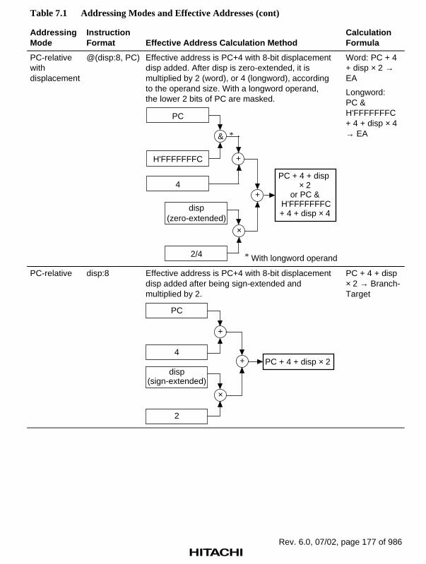
Rev. 6.0, 07/02, page 177 of 986
Table 7.1 Addressing Modes and Effective Addresses (cont)
AddressingMode
InstructionFormat Effective Address Calculation Method
CalculationFormula
PC-relativewithdisplacement
@(disp:8, PC) Effective address is PC+4 with 8-bit displacementdisp added. After disp is zero-extended, it ismultiplied by 2 (word), or 4 (longword), accordingto the operand size. With a longword operand,the lower 2 bits of PC are masked.
PC
H'FFFFFFFC
PC + 4 + disp × 2
or PC & H'FFFFFFFC+ 4 + disp × 4
+4
2/4
×
+
& *
disp(zero-extended)
* With longword operand
Word: PC + 4+ disp × 2 →EA
Longword:PC &H'FFFFFFFC+ 4 + disp × 4→ EA
PC-relative disp:8 Effective address is PC+4 with 8-bit displacementdisp added after being sign-extended andmultiplied by 2.
2
+
×
disp(sign-extended)
4
+
PC
PC + 4 + disp × 2
PC + 4 + disp× 2 → Branch-Target

Rev. 6.0, 07/02, page 178 of 986
Table 7.1 Addressing Modes and Effective Addresses (cont)
AddressingMode
InstructionFormat Effective Address Calculation Method
CalculationFormula
PC-relative disp:12 Effective address is PC+4 with 12-bit displacementdisp added after being sign-extended andmultiplied by 2.
2
+
×
disp(sign-extended)
4
+
PC
PC + 4 + disp × 2
PC + 4 + disp× 2 → Branch-Target
Rn Effective address is sum of PC+4 and Rn.
PC
4
Rn
+
+ PC + 4 + Rn
PC + 4 + Rn→ Branch-Target
Immediate #imm:8 8-bit immediate data imm of TST, AND, OR, orXOR instruction is zero-extended.
—
#imm:8 8-bit immediate data imm of MOV, ADD, orCMP/EQ instruction is sign-extended.
—
#imm:8 8-bit immediate data imm of TRAPA instruction iszero-extended and multiplied by 4.
—
Note: For the addressing modes below that use a displacement (disp), the assembler descriptionsin this manual show the value before scaling (×1, ×2, or ×4) is performed according to theoperand size. This is done to clarify the operation of the chip. Refer to the relevantassembler notation rules for the actual assembler descriptions.@ (disp:4, Rn) ; Register indirect with displacement
@ (disp:8, GBR) ; GBR indirect with displacement@ (disp:8, PC) ; PC-relative with displacementdisp:8, disp:12 ; PC-relative

Rev. 6.0, 07/02, page 179 of 986
7.3 Instruction Set
Table 7.2 shows the notation used in the following SH instruction list.
Table 7.2 Notation Used in Instruction List
Item Format Description
Instructionmnemonic
OP.Sz SRC, DEST OP: Operation codeSz: SizeSRC: SourceDEST: Source and/or destination operand
Summary ofoperation
→, ←: Transfer direction(xx): Memory operandM/Q/T: SR flag bits&: Logical AND of individual bits|: Logical OR of individual bits∧ : Logical exclusive-OR of individual bits~: Logical NOT of individual bits<<n, >>n: n-bit shift
Instruction code MSB ↔ LSB mmmm: Register number (Rm, FRm)nnnn: Register number (Rn, FRn)0000: R0, FR00001: R1, FR1 :1111: R15, FR15mmm: Register number (DRm, XDm, Rm_BANK)nnn: Register number (DRm, XDm, Rn_BANK)000: DR0, XD0, R0_BANK001: DR2, XD2, R1_BANK :111: DR14, XD14, R7_BANKmm: Register number (FVm)nn: Register number (FVn)00: FV001: FV410: FV811: FV12iiii: Immediate datadddd: Displacement
Privileged mode “Privileged” means the instruction can only be executedin privileged mode.
T bit Value of T bit afterinstruction execution
—: No change
Note: Scaling (×1, ×2, ×4, or ×8) is executed according to the size of the instruction operand(s).
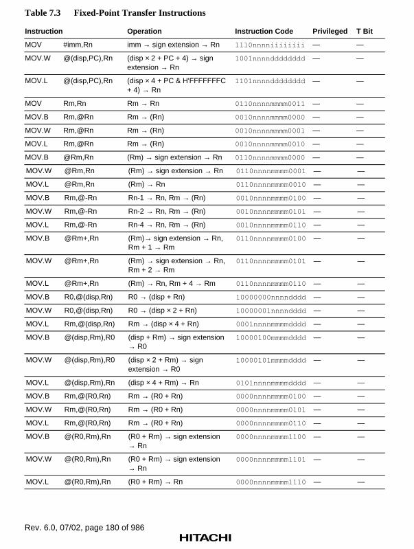
Rev. 6.0, 07/02, page 180 of 986
Table 7.3 Fixed-Point Transfer Instructions
Instruction Operation Instruction Code Privileged T Bit
MOV #imm,Rn imm → sign extension → Rn 1110nnnniiiiiiii — —
MOV.W @(disp,PC),Rn (disp × 2 + PC + 4) → signextension → Rn
1001nnnndddddddd — —
MOV.L @(disp,PC),Rn (disp × 4 + PC & H'FFFFFFFC+ 4) → Rn
1101nnnndddddddd — —
MOV Rm,Rn Rm → Rn 0110nnnnmmmm0011 — —
MOV.B Rm,@Rn Rm → (Rn) 0010nnnnmmmm0000 — —
MOV.W Rm,@Rn Rm → (Rn) 0010nnnnmmmm0001 — —
MOV.L Rm,@Rn Rm → (Rn) 0010nnnnmmmm0010 — —
MOV.B @Rm,Rn (Rm) → sign extension → Rn 0110nnnnmmmm0000 — —
MOV.W @Rm,Rn (Rm) → sign extension → Rn 0110nnnnmmmm0001 — —
MOV.L @Rm,Rn (Rm) → Rn 0110nnnnmmmm0010 — —
MOV.B Rm,@-Rn Rn-1 → Rn, Rm → (Rn) 0010nnnnmmmm0100 — —
MOV.W Rm,@-Rn Rn-2 → Rn, Rm → (Rn) 0010nnnnmmmm0101 — —
MOV.L Rm,@-Rn Rn-4 → Rn, Rm → (Rn) 0010nnnnmmmm0110 — —
MOV.B @Rm+,Rn (Rm)→ sign extension → Rn,Rm + 1 → Rm
0110nnnnmmmm0100 — —
MOV.W @Rm+,Rn (Rm) → sign extension → Rn,Rm + 2 → Rm
0110nnnnmmmm0101 — —
MOV.L @Rm+,Rn (Rm) → Rn, Rm + 4 → Rm 0110nnnnmmmm0110 — —
MOV.B R0,@(disp,Rn) R0 → (disp + Rn) 10000000nnnndddd — —
MOV.W R0,@(disp,Rn) R0 → (disp × 2 + Rn) 10000001nnnndddd — —
MOV.L Rm,@(disp,Rn) Rm → (disp × 4 + Rn) 0001nnnnmmmmdddd — —
MOV.B @(disp,Rm),R0 (disp + Rm) → sign extension→ R0
10000100mmmmdddd — —
MOV.W @(disp,Rm),R0 (disp × 2 + Rm) → signextension → R0
10000101mmmmdddd — —
MOV.L @(disp,Rm),Rn (disp × 4 + Rm) → Rn 0101nnnnmmmmdddd — —
MOV.B Rm,@(R0,Rn) Rm → (R0 + Rn) 0000nnnnmmmm0100 — —
MOV.W Rm,@(R0,Rn) Rm → (R0 + Rn) 0000nnnnmmmm0101 — —
MOV.L Rm,@(R0,Rn) Rm → (R0 + Rn) 0000nnnnmmmm0110 — —
MOV.B @(R0,Rm),Rn (R0 + Rm) → sign extension→ Rn
0000nnnnmmmm1100 — —
MOV.W @(R0,Rm),Rn (R0 + Rm) → sign extension→ Rn
0000nnnnmmmm1101 — —
MOV.L @(R0,Rm),Rn (R0 + Rm) → Rn 0000nnnnmmmm1110 — —

Rev. 6.0, 07/02, page 181 of 986
Table 7.3 Fixed-Point Transfer Instructions (cont)
Instruction Operation Instruction Code Privileged T Bit
MOV.B R0,@(disp,GBR) R0 → (disp + GBR) 11000000dddddddd — —
MOV.W R0,@(disp,GBR) R0 → (disp × 2 + GBR) 11000001dddddddd — —
MOV.L R0,@(disp,GBR) R0 → (disp × 4 + GBR) 11000010dddddddd — —
MOV.B @(disp,GBR),R0 (disp + GBR) →sign extension → R0
11000100dddddddd — —
MOV.W @(disp,GBR),R0 (disp × 2 + GBR) →sign extension → R0
11000101dddddddd — —
MOV.L @(disp,GBR),R0 (disp × 4 + GBR) → R0 11000110dddddddd — —
MOVA @(disp,PC),R0 disp × 4 + PC & H'FFFFFFFC+ 4 → R0
11000111dddddddd — —
MOVT Rn T → Rn 0000nnnn00101001 — —
SWAP.B Rm,Rn Rm → swap lower 2 bytes→ Rn
0110nnnnmmmm1000 — —
SWAP.W Rm,Rn Rm → swap upper/lowerwords → Rn
0110nnnnmmmm1001 — —
XTRCT Rm,Rn Rm:Rn middle 32 bits → Rn 0010nnnnmmmm1101 — —

Rev. 6.0, 07/02, page 182 of 986
Table 7.4 Arithmetic Operation Instructions
Instruction Operation Instruction Code Privileged T Bit
ADD Rm,Rn Rn + Rm → Rn 0011nnnnmmmm1100 — —
ADD #imm,Rn Rn + imm → Rn 0111nnnniiiiiiii — —
ADDC Rm,Rn Rn + Rm + T → Rn, carry → T 0011nnnnmmmm1110 — Carry
ADDV Rm,Rn Rn + Rm → Rn, overflow → T 0011nnnnmmmm1111 — Overflow
CMP/EQ #imm,R0 When R0 = imm, 1 → TOtherwise, 0 → T
10001000iiiiiiii — Comparisonresult
CMP/EQ Rm,Rn When Rn = Rm, 1 → TOtherwise, 0 → T
0011nnnnmmmm0000 — Comparisonresult
CMP/HS Rm,Rn When Rn ≥ Rm (unsigned),1 → TOtherwise, 0 → T
0011nnnnmmmm0010 — Comparisonresult
CMP/GE Rm,Rn When Rn ≥ Rm (signed), 1 → TOtherwise, 0 → T
0011nnnnmmmm0011 — Comparisonresult
CMP/HI Rm,Rn When Rn > Rm (unsigned),1 → TOtherwise, 0 → T
0011nnnnmmmm0110 — Comparisonresult
CMP/GT Rm,Rn When Rn > Rm (signed), 1 → TOtherwise, 0 → T
0011nnnnmmmm0111 — Comparisonresult
CMP/PZ Rn When Rn ≥ 0, 1 → TOtherwise, 0 → T
0100nnnn00010001 — Comparisonresult
CMP/PL Rn When Rn > 0, 1 → TOtherwise, 0 → T
0100nnnn00010101 — Comparisonresult
CMP/STR Rm,Rn When any bytes are equal,1 → TOtherwise, 0 → T
0010nnnnmmmm1100 — Comparisonresult
DIV1 Rm,Rn 1-step division (Rn ÷ Rm) 0011nnnnmmmm0100 — Calculationresult
DIV0S Rm,Rn MSB of Rn → Q,MSB of Rm → M, M^Q → T
0010nnnnmmmm0111 — Calculationresult
DIV0U 0 → M/Q/T 0000000000011001 — 0
DMULS.L Rm,Rn Signed, Rn × Rm → MAC,32 × 32 → 64 bits
0011nnnnmmmm1101 — —
DMULU.L Rm,Rn Unsigned, Rn × Rm → MAC,32 × 32 → 64 bits
0011nnnnmmmm0101 — —
DT Rn Rn – 1 → Rn; when Rn = 0,1 → TWhen Rn ≠ 0, 0 → T
0100nnnn00010000 — Comparisonresult
EXTS.B Rm,Rn Rm sign-extended frombyte → Rn
0110nnnnmmmm1110 — —

Rev. 6.0, 07/02, page 183 of 986
Table 7.4 Arithmetic Operation Instructions (cont)
Instruction Operation Instruction Code Privileged T Bit
EXTS.W Rm,Rn Rm sign-extended fromword → Rn
0110nnnnmmmm1111 — —
EXTU.B Rm,Rn Rm zero-extended frombyte → Rn
0110nnnnmmmm1100 — —
EXTU.W Rm,Rn Rm zero-extended fromword → Rn
0110nnnnmmmm1101 — —
MAC.L @Rm+,@Rn+ Signed, (Rn) × (Rm) + MAC →MACRn + 4 → Rn, Rm + 4 → Rm32 × 32 + 64 → 64 bits
0000nnnnmmmm1111 — —
MAC.W @Rm+,@Rn+ Signed, (Rn) × (Rm) + MAC →MACRn + 2 → Rn, Rm + 2 → Rm16 × 16 + 64 → 64 bits
0100nnnnmmmm1111 — —
MUL.L Rm,Rn Rn × Rm → MACL32 × 32 → 32 bits
0000nnnnmmmm0111 — —
MULS.W Rm,Rn Signed, Rn × Rm → MACL16 × 16 → 32 bits
0010nnnnmmmm1111 — —
MULU.W Rm,Rn Unsigned, Rn × Rm → MACL16 × 16 → 32 bits
0010nnnnmmmm1110 — —
NEG Rm,Rn 0 – Rm → Rn 0110nnnnmmmm1011 — —
NEGC Rm,Rn 0 – Rm – T → Rn, borrow → T 0110nnnnmmmm1010 — Borrow
SUB Rm,Rn Rn – Rm → Rn 0011nnnnmmmm1000 — —
SUBC Rm,Rn Rn – Rm – T → Rn, borrow → T 0011nnnnmmmm1010 — Borrow
SUBV Rm,Rn Rn – Rm → Rn, underflow → T 0011nnnnmmmm1011 — Underflow

Rev. 6.0, 07/02, page 184 of 986
Table 7.5 Logic Operation Instructions
Instruction Operation Instruction Code Privileged T Bit
AND Rm,Rn Rn & Rm → Rn 0010nnnnmmmm1001 — —
AND #imm,R0 R0 & imm → R0 11001001iiiiiiii — —
AND.B #imm,@(R0,GBR) (R0 + GBR) & imm → (R0 +GBR)
11001101iiiiiiii — —
NOT Rm,Rn ~Rm → Rn 0110nnnnmmmm0111 — —
OR Rm,Rn Rn | Rm → Rn 0010nnnnmmmm1011 — —
OR #imm,R0 R0 | imm → R0 11001011iiiiiiii — —
OR.B #imm,@(R0,GBR) (R0 + GBR) | imm → (R0 +GBR)
11001111iiiiiiii —
TAS.B @Rn When (Rn) = 0, 1 → TOtherwise, 0 → TIn both cases, 1 → MSB of (Rn)
0100nnnn00011011 — Test result
TST Rm,Rn Rn & Rm; when result = 0,1 → TOtherwise, 0 → T
0010nnnnmmmm1000 — Test result
TST #imm,R0 R0 & imm; when result = 0,1 → TOtherwise, 0 → T
11001000iiiiiiii — Test result
TST.B #imm,@(R0,GBR) (R0 + GBR) & imm; when result= 0, 1 → TOtherwise, 0 → T
11001100iiiiiiii — Test result
XOR Rm,Rn Rn ∧ Rm → Rn 0010nnnnmmmm1010 — —
XOR #imm,R0 R0 ∧ imm → R0 11001010iiiiiiii — —
XOR.B #imm,@(R0,GBR) (R0 + GBR) ∧ imm → (R0 +GBR)
11001110iiiiiiii — —

Rev. 6.0, 07/02, page 185 of 986
Table 7.6 Shift Instructions
Instruction Operation Instruction Code Privileged T Bit
ROTL Rn T ← Rn ← MSB 0100nnnn00000100 — MSB
ROTR Rn LSB → Rn → T 0100nnnn00000101 — LSB
ROTCL Rn T ← Rn ← T 0100nnnn00100100 — MSB
ROTCR Rn T → Rn → T 0100nnnn00100101 — LSB
SHAD Rm,Rn When Rn ≥ 0, Rn << Rm → RnWhen Rn < 0, Rn >> Rm →[MSB → Rn]
0100nnnnmmmm1100 — —
SHAL Rn T ← Rn ← 0 0100nnnn00100000 — MSB
SHAR Rn MSB → Rn → T 0100nnnn00100001 — LSB
SHLD Rm,Rn When Rn ≥ 0, Rn << Rm → RnWhen Rn < 0, Rn >> Rm →[0 → Rn]
0100nnnnmmmm1101 — —
SHLL Rn T ← Rn ← 0 0100nnnn00000000 — MSB
SHLR Rn 0 → Rn → T 0100nnnn00000001 — LSB
SHLL2 Rn Rn << 2 → Rn 0100nnnn00001000 — —
SHLR2 Rn Rn >> 2 → Rn 0100nnnn00001001 — —
SHLL8 Rn Rn << 8 → Rn 0100nnnn00011000 — —
SHLR8 Rn Rn >> 8 → Rn 0100nnnn00011001 — —
SHLL16 Rn Rn << 16 → Rn 0100nnnn00101000 — —
SHLR16 Rn Rn >> 16 → Rn 0100nnnn00101001 — —

Rev. 6.0, 07/02, page 186 of 986
Table 7.7 Branch Instructions
Instruction Operation Instruction Code Privileged T Bit
BF label When T = 0, disp × 2 + PC +4 → PCWhen T = 1, nop
10001011dddddddd — —
BF/S label Delayed branch; when T = 0,disp × 2 + PC + 4 → PCWhen T = 1, nop
10001111dddddddd — —
BT label When T = 1, disp × 2 + PC +4 → PCWhen T = 0, nop
10001001dddddddd — —
BT/S label Delayed branch; when T = 1,disp × 2 + PC + 4 → PCWhen T = 0, nop
10001101dddddddd — —
BRA label Delayed branch, disp × 2 +PC + 4 → PC
1010dddddddddddd — —
BRAF Rn Delayed branch, Rn + PC +4 → PC
0000nnnn00100011 — —
BSR label Delayed branch, PC + 4 → PR,disp × 2 + PC + 4 → PC
1011dddddddddddd — —
BSRF Rn Delayed branch, PC + 4 → PR,Rn + PC + 4 → PC
0000nnnn00000011 — —
JMP @Rn Delayed branch, Rn → PC 0100nnnn00101011 — —
JSR @Rn Delayed branch, PC + 4 → PR,Rn → PC
0100nnnn00001011 — —
RTS Delayed branch, PR → PC 0000000000001011 — —

Rev. 6.0, 07/02, page 187 of 986
Table 7.8 System Control Instructions
Instruction Operation Instruction Code Privileged T Bit
CLRMAC 0 → MACH, MACL 0000000000101000 — —
CLRS 0 → S 0000000001001000 — —
CLRT 0 → T 0000000000001000 — 0
LDC Rm,SR Rm → SR 0100mmmm00001110 Privileged LSB
LDC Rm,GBR Rm → GBR 0100mmmm00011110 — —
LDC Rm,VBR Rm → VBR 0100mmmm00101110 Privileged —
LDC Rm,SSR Rm → SSR 0100mmmm00111110 Privileged —
LDC Rm,SPC Rm → SPC 0100mmmm01001110 Privileged —
LDC Rm,DBR Rm → DBR 0100mmmm11111010 Privileged —
LDC Rm,Rn_BANK Rm → Rn_BANK (n = 0 to 7) 0100mmmm1nnn1110 Privileged —
LDC.L @Rm+,SR (Rm) → SR, Rm + 4 → Rm 0100mmmm00000111 Privileged LSB
LDC.L @Rm+,GBR (Rm) → GBR, Rm + 4 → Rm 0100mmmm00010111 — —
LDC.L @Rm+,VBR (Rm) → VBR, Rm + 4 → Rm 0100mmmm00100111 Privileged —
LDC.L @Rm+,SSR (Rm) → SSR, Rm + 4 → Rm 0100mmmm00110111 Privileged —
LDC.L @Rm+,SPC (Rm) → SPC, Rm + 4 → Rm 0100mmmm01000111 Privileged —
LDC.L @Rm+,DBR (Rm) → DBR, Rm + 4 → Rm 0100mmmm11110110 Privileged —
LDC.L @Rm+,Rn_BANK (Rm) → Rn_BANK,Rm + 4 → Rm
0100mmmm1nnn0111 Privileged —
LDS Rm,MACH Rm → MACH 0100mmmm00001010 — —
LDS Rm,MACL Rm → MACL 0100mmmm00011010 — —
LDS Rm,PR Rm → PR 0100mmmm00101010 — —
LDS.L @Rm+,MACH (Rm) → MACH, Rm + 4 → Rm 0100mmmm00000110 — —
LDS.L @Rm+,MACL (Rm) → MACL, Rm + 4 → Rm 0100mmmm00010110 — —
LDS.L @Rm+,PR (Rm) → PR, Rm + 4 → Rm 0100mmmm00100110 — —
LDTLB PTEH/PTEL → TLB 0000000000111000 Privileged —
MOVCA.L R0,@Rn R0 → (Rn) (without fetchingcache block)
0000nnnn11000011 — —
NOP No operation 0000000000001001 — —
OCBI @Rn Invalidates operand cache block 0000nnnn10010011 — —
OCBP @Rn Writes back and invalidatesoperand cache block
0000nnnn10100011 — —
OCBWB @Rn Writes back operand cacheblock
0000nnnn10110011 — —
PREF @Rn (Rn) → operand cache 0000nnnn10000011 — —
RTE Delayed branch, SSR/SPC →SR/PC
0000000000101011 Privileged —

Rev. 6.0, 07/02, page 188 of 986
Table 7.8 System Control Instructions (cont)
Instruction Operation Instruction Code Privileged T Bit
SETS 1 → S 0000000001011000 — —
SETT 1 → T 0000000000011000 — 1
SLEEP Sleep or standby 0000000000011011 Privileged —
STC SR,Rn SR → Rn 0000nnnn00000010 Privileged —
STC GBR,Rn GBR → Rn 0000nnnn00010010 — —
STC VBR,Rn VBR → Rn 0000nnnn00100010 Privileged —
STC SSR,Rn SSR → Rn 0000nnnn00110010 Privileged —
STC SPC,Rn SPC → Rn 0000nnnn01000010 Privileged —
STC SGR,Rn SGR → Rn 0000nnnn00111010 Privileged —
STC DBR,Rn DBR → Rn 0000nnnn11111010 Privileged —
STC Rm_BANK,Rn Rm_BANK → Rn (m = 0 to 7) 0000nnnn1mmm0010 Privileged —
STC.L SR,@-Rn Rn – 4 → Rn, SR → (Rn) 0100nnnn00000011 Privileged —
STC.L GBR,@-Rn Rn – 4 → Rn, GBR → (Rn) 0100nnnn00010011 — —
STC.L VBR,@-Rn Rn – 4 → Rn, VBR → (Rn) 0100nnnn00100011 Privileged —
STC.L SSR,@-Rn Rn – 4 → Rn, SSR → (Rn) 0100nnnn00110011 Privileged —
STC.L SPC,@-Rn Rn – 4 → Rn, SPC → (Rn) 0100nnnn01000011 Privileged —
STC.L SGR,@-Rn Rn – 4 → Rn, SGR → (Rn) 0100nnnn00110010 Privileged —
STC.L DBR,@-Rn Rn – 4 → Rn, DBR → (Rn) 0100nnnn11110010 Privileged —
STC.L Rm_BANK,@-Rn Rn – 4 → Rn,Rm_BANK → (Rn) (m = 0 to 7)
0100nnnn1mmm0011 Privileged —
STS MACH,Rn MACH → Rn 0000nnnn00001010 — —
STS MACL,Rn MACL → Rn 0000nnnn00011010 — —
STS PR,Rn PR → Rn 0000nnnn00101010 — —
STS.L MACH,@-Rn Rn – 4 → Rn, MACH → (Rn) 0100nnnn00000010 — —
STS.L MACL,@-Rn Rn – 4 → Rn, MACL → (Rn) 0100nnnn00010010 — —
STS.L PR,@-Rn Rn – 4 → Rn, PR → (Rn) 0100nnnn00100010 — —
TRAPA #imm PC + 2 → SPC, SR → SSR,#imm << 2 → TRA,H'160 → EXPEVT,VBR + H'0100 → PC
11000011iiiiiiii — —

Rev. 6.0, 07/02, page 189 of 986
Table 7.9 Floating-Point Single-Precision Instructions
Instruction Operation Instruction Code Privileged T Bit
FLDI0 FRn H'00000000 → FRn 1111nnnn10001101 — —
FLDI1 FRn H'3F800000 → FRn 1111nnnn10011101 — —
FMOV FRm,FRn FRm → FRn 1111nnnnmmmm1100 — —
FMOV.S @Rm,FRn (Rm) → FRn 1111nnnnmmmm1000 — —
FMOV.S @(R0,Rm),FRn (R0 + Rm) → FRn 1111nnnnmmmm0110 — —
FMOV.S @Rm+,FRn (Rm) → FRn, Rm + 4 → Rm 1111nnnnmmmm1001 — —
FMOV.S FRm,@Rn FRm → (Rn) 1111nnnnmmmm1010 — —
FMOV.S FRm,@-Rn Rn-4 → Rn, FRm → (Rn) 1111nnnnmmmm1011 — —
FMOV.S FRm,@(R0,Rn) FRm → (R0 + Rn) 1111nnnnmmmm0111 — —
FMOV DRm,DRn DRm → DRn 1111nnn0mmm01100 — —
FMOV @Rm,DRn (Rm) → DRn 1111nnn0mmmm1000 — —
FMOV @(R0,Rm),DRn (R0 + Rm) → DRn 1111nnn0mmmm0110 — —
FMOV @Rm+,DRn (Rm) → DRn, Rm + 8 → Rm 1111nnn0mmmm1001 — —
FMOV DRm,@Rn DRm → (Rn) 1111nnnnmmm01010 — —
FMOV DRm,@-Rn Rn-8 → Rn, DRm → (Rn) 1111nnnnmmm01011 — —
FMOV DRm,@(R0,Rn) DRm → (R0 + Rn) 1111nnnnmmm00111 — —
FLDS FRm,FPUL FRm → FPUL 1111mmmm00011101 — —
FSTS FPUL,FRn FPUL → FRn 1111nnnn00001101 — —
FABS FRn FRn & H'7FFF FFFF → FRn 1111nnnn01011101 — —
FADD FRm,FRn FRn + FRm → FRn 1111nnnnmmmm0000 — —
FCMP/EQ FRm,FRn When FRn = FRm, 1 → TOtherwise, 0 → T
1111nnnnmmmm0100 — Comparisonresult
FCMP/GT FRm,FRn When FRn > FRm, 1 → TOtherwise, 0 → T
1111nnnnmmmm0101 — Comparisonresult
FDIV FRm,FRn FRn/FRm → FRn 1111nnnnmmmm0011 — —
FLOAT FPUL,FRn (float) FPUL → FRn 1111nnnn00101101 — —
FMAC FR0,FRm,FRn FR0 * FRm + FRn → FRn 1111nnnnmmmm1110 — —
FMUL FRm,FRn FRn * FRm → FRn 1111nnnnmmmm0010 — —
FNEG FRn FRn ∧ H'80000000 → FRn 1111nnnn01001101 — —
FSQRT FRn FRn → FRn 1111nnnn01101101 — —
FSUB FRm,FRn FRn – FRm → FRn 1111nnnnmmmm0001 — —
FTRC FRm,FPUL (long) FRm → FPUL 1111mmmm00111101 — —

Rev. 6.0, 07/02, page 190 of 986
Table 7.10 Floating-Point Double-Precision Instructions
Instruction Operation Instruction Code Privileged T Bit
FABS DRn DRn & H'7FFF FFFF FFFFFFFF → DRn
1111nnn001011101 — —
FADD DRm,DRn DRn + DRm → DRn 1111nnn0mmm00000 — —
FCMP/EQ DRm,DRn When DRn = DRm, 1 → TOtherwise, 0 → T
1111nnn0mmm00100 — Comparisonresult
FCMP/GT DRm,DRn When DRn > DRm, 1 → TOtherwise, 0 → T
1111nnn0mmm00101 — Comparisonresult
FDIV DRm,DRn DRn /DRm → DRn 1111nnn0mmm00011 — —
FCNVDS DRm,FPUL double_to_ float[DRm] → FPUL 1111mmm010111101 — —
FCNVSD FPUL,DRn float_to_ double [FPUL] → DRn 1111nnn010101101 — —
FLOAT FPUL,DRn (float)FPUL → DRn 1111nnn000101101 — —
FMUL DRm,DRn DRn * DRm → DRn 1111nnn0mmm00010 — —
FNEG DRn DRn ^ H'8000 0000 0000 0000→ DRn
1111nnn001001101 — —
FSQRT DRn DRn DRn 1111nnn001101101 — —
FSUB DRm,DRn DRn – DRm → DRn 1111nnn0mmm00001 — —
FTRC DRm,FPUL (long) DRm → FPUL 1111mmm000111101 — —
Table 7.11 Floating-Point Control Instructions
Instruction Operation Instruction Code Privileged T Bit
LDS Rm,FPSCR Rm → FPSCR 0100mmmm01101010 — —
LDS Rm,FPUL Rm → FPUL 0100mmmm01011010 — —
LDS.L @Rm+,FPSCR (Rm) → FPSCR, Rm+4 → Rm 0100mmmm01100110 — —
LDS.L @Rm+,FPUL (Rm) → FPUL, Rm+4 → Rm 0100mmmm01010110 — —
STS FPSCR,Rn FPSCR → Rn 0000nnnn01101010 — —
STS FPUL,Rn FPUL → Rn 0000nnnn01011010 — —
STS.L FPSCR,@-Rn Rn – 4 → Rn, FPSCR → (Rn) 0100nnnn01100010 — —
STS.L FPUL,@-Rn Rn – 4 → Rn, FPUL → (Rn) 0100nnnn01010010 — —
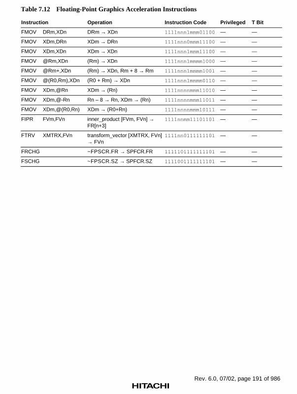
Rev. 6.0, 07/02, page 191 of 986
Table 7.12 Floating-Point Graphics Acceleration Instructions
Instruction Operation Instruction Code Privileged T Bit
FMOV DRm,XDn DRm → XDn 1111nnn1mmm01100 — —
FMOV XDm,DRn XDm → DRn 1111nnn0mmm11100 — —
FMOV XDm,XDn XDm → XDn 1111nnn1mmm11100 — —
FMOV @Rm,XDn (Rm) → XDn 1111nnn1mmmm1000 — —
FMOV @Rm+,XDn (Rm) → XDn, Rm + 8 → Rm 1111nnn1mmmm1001 — —
FMOV @(R0,Rm),XDn (R0 + Rm) → XDn 1111nnn1mmmm0110 — —
FMOV XDm,@Rn XDm → (Rn) 1111nnnnmmm11010 — —
FMOV XDm,@-Rn Rn – 8 → Rn, XDm → (Rn) 1111nnnnmmm11011 — —
FMOV XDm,@(R0,Rn) XDm → (R0+Rn) 1111nnnnmmm10111 — —
FIPR FVm,FVn inner_product [FVm, FVn] →FR[n+3]
1111nnmm11101101 — —
FTRV XMTRX,FVn transform_vector [XMTRX, FVn]→ FVn
1111nn0111111101 — —
FRCHG ~FPSCR.FR → SPFCR.FR 1111101111111101 — —
FSCHG ~FPSCR.SZ → SPFCR.SZ 1111001111111101 — —

Rev. 6.0, 07/02, page 192 of 986
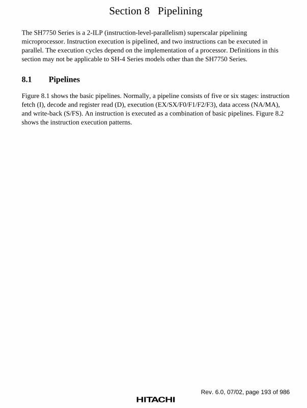
Rev. 6.0, 07/02, page 193 of 986
Section 8 Pipelining
The SH7750 Series is a 2-ILP (instruction-level-parallelism) superscalar pipeliningmicroprocessor. Instruction execution is pipelined, and two instructions can be executed inparallel. The execution cycles depend on the implementation of a processor. Definitions in thissection may not be applicable to SH-4 Series models other than the SH7750 Series.
8.1 Pipelines
Figure 8.1 shows the basic pipelines. Normally, a pipeline consists of five or six stages: instructionfetch (I), decode and register read (D), execution (EX/SX/F0/F1/F2/F3), data access (NA/MA),and write-back (S/FS). An instruction is executed as a combination of basic pipelines. Figure 8.2shows the instruction execution patterns.

Rev. 6.0, 07/02, page 194 of 986
1. General Pipeline
• Instruction fetch • Instruction decode
• Issue• Register read• Destination address calculation
for PC-relative branch
• Non-memory data access
• Write-back
I D EX
• Operation
NA S
2. General Load/Store Pipeline
• Instruction fetch • Instruction decode
• Issue• Register read
• Memory data access
• Write-back
I D EX
• Address calculation
MA S
3. Special Pipeline
• Instruction fetch • Instruction decode
• Issue• Register read
• Non-memory data access
• Write-back
I D SX
• Operation
NA S
4. Special Load/Store Pipeline
• Instruction fetch • Instruction decode
• Issue• Register read
• Memory data access
• Write-back
I D SX
• Address calculation
MA S
5. Floating-Point Pipeline
• Instruction fetch • Instruction decode
• Issue• Register read
• Computation 2 • Computation 3• Write-back
I D F1
• Computation 1
F2 FS
6. Floating-Point Extended Pipeline
• Instruction fetch • Instruction decode
• Issue• Register read
• Computation 1 • Computation 3• Write-back
I D F0
• Computation 0
F1 F2 FS
• Computation 2
F3
Computation: Takes several cycles
7. FDIV/FSQRT Pipeline
Figure 8.1 Basic Pipelines

Rev. 6.0, 07/02, page 195 of 986
1. 1-step operation: 1 issue cycleEXT[SU].[BW], MOV, MOV#, MOVA, MOVT, SWAP.[BW], XTRCT, ADD*, CMP*, DIV*, DT, NEG*, SUB*, AND, AND#, NOT, OR, OR#, TST, TST#, XOR, XOR#, ROT*, SHA*, SHL*, BF*, BT*, BRA, NOP, CLRS, CLRT, SETS, SETT, LDS to FPUL, STS from FPUL/FPSCR, FLDI0, FLDI1, FMOV, FLDS, FSTS, single-/double-precision FABS/FNEG
I D EX NA S
2. Load/store: 1 issue cycleMOV.[BWL]. FMOV*@, LDS.L to FPUL, LDTLB, PREF, STS.L from FPUL/FPSCR
I D EX MA S
3. GBR-based load/store: 1 issue cycleMOV.[BWL]@(d,GBR)
I D SX MA S
4. JMP, RTS, BRAF: 2 issue cyclesI D EX NA S
D EX NA S
5. TST.B: 3 issue cycles
I D SX MA SD SX NA S
D SX NA S
6. AND.B, OR.B, XOR.B: 4 issue cyclesI D SX MA S
D SX NA SD SX NA S
D SX MA S
7. TAS.B: 5 issue cycles
I D EX MA SD EX MA S
D EX NA SD EX NA S
D EX MA S
8. RTE: 5 issue cyclesI D EX NA S
D EX NA SD EX NA S
D EX NA SD EX NA S
9. SLEEP: 4 issue cycles
I D EX NA SD EX NA S
D EX NA SD EX NA S
Figure 8.2 Instruction Execution Patterns

Rev. 6.0, 07/02, page 196 of 986
10. OCBI: 1 issue cycleI D EX MA S
MA
11. OCBP, OCBWB: 1 issue cycleI D EX MA S
MAMA
MAMA
12. MOVCA.L: 1 issue cycleI D EX MA S
MAMA
MAMA
MAMA
13. TRAPA: 7 issue cyclesI D EX NA S
D EX NA SD EX NA S
D EX NA SD EX NA S
D EX NA SD EX NA S
14. LDC to DBR/Rp_BANK/SSR/SPC/VBR, BSR: 1 issue cycle
I D EX NA SSX
SX
15. LDC to GBR: 3 issue cyclesI D EX NA S
DDSX
SX
16. LDC to SR: 4 issue cyclesI D EX NA S
DD
D
SXSX
SX
I D EX MA S
17. LDC.L to DBR/Rp_BANK/SSR/SPC/VBR: 1 issue cycle
SXSX
18. LDC.L to GBR: 3 issue cycles
I D EX MA SD
DSX
SX
Figure 8.2 Instruction Execution Patterns (cont)

Rev. 6.0, 07/02, page 197 of 986
19. LDC.L to SR: 4 issue cyclesI D EX MA S
DD
D
SXSX
SX
20. STC from DBR/GBR/Rp_BANK/SR/SSR/SPC/VBR: 2 issue cyclesI D SX NA S
D SX NA S
21. STC.L from SGR: 3 issue cyclesI D SX NA S
D SX NA SD SX NA S
22. STC.L from DBR/GBR/Rp_BANK/SR/SSR/SPC/VBR: 2 issue cycles
I D SX NA SD SX MA S
23. STC.L from SGR: 3 issue cyclesI D SX NA S
D SX NA SD SX MA S
24. LDS to PR, JSR, BSRF: 2 issue cyclesI D EX NA S
D SXSX
25. LDS.L to PR: 2 issue cyclesI D EX MA S
D SXSX
26. STS from PR: 2 issue cyclesI D SX NA S
D SX NA S
27. STS.L from PR: 2 issue cycles
I D SX NA SD SX MA S
28. CLRMAC, LDS to MACH/L: 1 issue cycleI D EX NA S
F1F1 F2 FS
29. LDS.L to MACH/L: 1 issue cycleI D EX MA S
F1F1 F2 FS
30. STS from MACH/L: 1 issue cycle
I D EX NA S
Figure 8.2 Instruction Execution Patterns (cont)

Rev. 6.0, 07/02, page 198 of 986
31. STS.L from MACH/L: 1 issue cycleI D EX MA S
32. LDS to FPSCR: 1 issue cycle
I D EX NA SF1
F1F1
F1F1
F1
33. LDS.L to FPSCR: 1 issue cycleI D EX MA S
34. Fixed-point multiplication: 2 issue cyclesDMULS.L, DMULU.L, MUL.L, MULS.W, MULU.W
I D EX NA S (CPU)D EX NA S
f1 (FPU)f1
f1f1 F2 FS
35. MAC.W, MAC.L: 2 issue cyclesI D EX MA S (CPU)
D EX MA S
f1 (FPU)f1
f1f1 F2 FS
36. Single-precision floating-point computation: 1 issue cycleFCMP/EQ,FCMP/GT, FADD,FLOAT,FMAC,FMUL,FSUB,FTRC,FRCHG,FSCHG
I D F1 F2 FS
37. Single-precision FDIV/SQRT: 1 issue cycle
I D F1 F2 FSF3
F1 F2 FS
38. Double-precision floating-point computation 1: 1 issue cycle FCNVDS, FCNVSD, FLOAT, FTRC
I D F1 F2 FSd F1 F2 FS
39. Double-precision floating-point computation 2: 1 issue cycle FADD, FMUL, FSUB
I D F1 F2 FSd F1 F2 FS
d F1 F2 FSd F1 F2 FS
d F1 F2 FS
F1 F2 FS
Figure 8.2 Instruction Execution Patterns (cont)

Rev. 6.0, 07/02, page 199 of 986
I D F1 F2 FSD F1 F2 FS
40. Double-precision FCMP: 2 issue cyclesFCMP/EQ,FCMP/GT
I D F1 F2 FS
F3F1 F2 FS
41. Double-precision FDIV/SQRT: 1 issue cycle FDIV, FSQRT
F1 F2d
F1 F2 FSF1 F2 FS
42. FIPR: 1 issue cycleI D F0 F1 F2 FS
43. FTRV: 1 issue cycleF1 F2 FSD F0I
F1 F2 FSd F0F1 F2 FSd F0
F1 F2 FSd F0
Notes: ??
: Locks D-stage
: Register read only
: Locks, but no operation is executed.
: Can overlap another f1, but not another F1.
d
D
??
f1
: Cannot overlap a stage of the same kind, except when two instructions are executed in parallel.
Figure 8.2 Instruction Execution Patterns (cont)

Rev. 6.0, 07/02, page 200 of 986
8.2 Parallel-Executability
Instructions are categorized into six groups according to the internal function blocks used, asshown in table 8.1. Table 8.2 shows the parallel-executability of pairs of instructions in terms ofgroups. For example, ADD in the EX group and BRA in the BR group can be executed in parallel.
Table 8.1 Instruction Groups
1. MT Group
CLRT CMP/HI Rm,Rn MOV Rm,Rn
CMP/EQ #imm,R0 CMP/HS Rm,Rn NOP
CMP/EQ Rm,Rn CMP/PL Rn SETT
CMP/GE Rm,Rn CMP/PZ Rn TST #imm,R0
CMP/GT Rm,Rn CMP/STR Rm,Rn TST Rm,Rn
2. EX Group
ADD #imm,Rn MOVT Rn SHLL2 Rn
ADD Rm,Rn NEG Rm,Rn SHLL8 Rn
ADDC Rm,Rn NEGC Rm,Rn SHLR Rn
ADDV Rm,Rn NOT Rm,Rn SHLR16 Rn
AND #imm,R0 OR #imm,R0 SHLR2 Rn
AND Rm,Rn OR Rm,Rn SHLR8 Rn
DIV0S Rm,Rn ROTCL Rn SUB Rm,Rn
DIV0U ROTCR Rn SUBC Rm,Rn
DIV1 Rm,Rn ROTL Rn SUBV Rm,Rn
DT Rn ROTR Rn SWAP.B Rm,Rn
EXTS.B Rm,Rn SHAD Rm,Rn SWAP.W Rm,Rn
EXTS.W Rm,Rn SHAL Rn XOR #imm,R0
EXTU.B Rm,Rn SHAR Rn XOR Rm,Rn
EXTU.W Rm,Rn SHLD Rm,Rn XTRCT Rm,Rn
MOV #imm,Rn SHLL Rn
MOVA @(disp,PC),R0 SHLL16 Rn
3. BR Group
BF disp BRA disp BT disp
BF/S disp BSR disp BT/S disp

Rev. 6.0, 07/02, page 201 of 986
Table 8.1 Instruction Groups (cont)
4. LS Group
FABS DRn FMOV.S @Rm+,FRn MOV.L R0,@(disp,GBR)
FABS FRn FMOV.S FRm,@(R0,Rn) MOV.L Rm,@(disp,Rn)
FLDI0 FRn FMOV.S FRm,@-Rn MOV.L Rm,@(R0,Rn)
FLDI1 FRn FMOV.S FRm,@Rn MOV.L Rm,@-Rn
FLDS FRm,FPUL FNEG DRn MOV.L Rm,@Rn
FMOV @(R0,Rm),DRn FNEG FRn MOV.W @(disp,GBR),R0
FMOV @(R0,Rm),XDn FSTS FPUL,FRn MOV.W @(disp,PC),Rn
FMOV @Rm,DRn LDS Rm,FPUL MOV.W @(disp,Rm),R0
FMOV @Rm,XDn MOV.B @(disp,GBR),R0 MOV.W @(R0,Rm),Rn
FMOV @Rm+,DRn MOV.B @(disp,Rm),R0 MOV.W @Rm,Rn
FMOV @Rm+,XDn MOV.B @(R0,Rm),Rn MOV.W @Rm+,Rn
FMOV DRm,@(R0,Rn) MOV.B @Rm,Rn MOV.W R0,@(disp,GBR)
FMOV DRm,@-Rn MOV.B @Rm+,Rn MOV.W R0,@(disp,Rn)
FMOV DRm,@Rn MOV.B R0,@(disp,GBR) MOV.W Rm,@(R0,Rn)
FMOV DRm,DRn MOV.B R0,@(disp,Rn) MOV.W Rm,@-Rn
FMOV DRm,XDn MOV.B Rm,@(R0,Rn) MOV.W Rm,@Rn
FMOV FRm,FRn MOV.B Rm,@-Rn MOVCA.L R0,@Rn
FMOV XDm,@(R0,Rn) MOV.B Rm,@Rn OCBI @Rn
FMOV XDm,@-Rn MOV.L @(disp,GBR),R0 OCBP @Rn
FMOV XDm,@Rn MOV.L @(disp,PC),Rn OCBWB @Rn
FMOV XDm,DRn MOV.L @(disp,Rm),Rn PREF @Rn
FMOV XDm,XDn MOV.L @(R0,Rm),Rn STS FPUL,Rn
FMOV.S @(R0,Rm),FRn MOV.L @Rm,Rn
FMOV.S @Rm,FRn MOV.L @Rm+,Rn

Rev. 6.0, 07/02, page 202 of 986
Table 8.1 Instruction Groups (cont)
5. FE Group
FADD DRm,DRn FIPR FVm,FVn FSQRT DRn
FADD FRm,FRn FLOAT FPUL,DRn FSQRT FRn
FCMP/EQ FRm,FRn FLOAT FPUL,FRn FSUB DRm,DRn
FCMP/GT FRm,FRn FMAC FR0,FRm,FRn FSUB FRm,FRn
FCNVDS DRm,FPUL FMUL DRm,DRn FTRC DRm,FPUL
FCNVSD FPUL,DRn FMUL FRm,FRn FTRC FRm,FPUL
FDIV DRm,DRn FRCHG FTRV XMTRX,FVn
FDIV FRm,FRn FSCHG

Rev. 6.0, 07/02, page 203 of 986
Table 8.1 Instruction Groups (cont)
6. CO Group
AND.B #imm,@(R0,GBR) LDS Rm,FPSCR STC SR,Rn
BRAF Rm LDS Rm,MACH STC SSR,Rn
BSRF Rm LDS Rm,MACL STC VBR,Rn
CLRMAC LDS Rm,PR STC.L DBR,@-Rn
CLRS LDS.L @Rm+,FPSCR STC.L GBR,@-Rn
DMULS.L Rm,Rn LDS.L @Rm+,FPUL STC.L Rp_BANK,@-Rn
DMULU.L Rm,Rn LDS.L @Rm+,MACH STC.L SGR,@-Rn
FCMP/EQ DRm,DRn LDS.L @Rm+,MACL STC.L SPC,@-Rn
FCMP/GT DRm,DRn LDS.L @Rm+,PR STC.L SR,@-Rn
JMP @Rn LDTLB STC.L SSR,@-Rn
JSR @Rn MAC.L @Rm+,@Rn+ STC.L VBR,@-Rn
LDC Rm,DBR MAC.W @Rm+,@Rn+ STS FPSCR,Rn
LDC Rm,GBR MUL.L Rm,Rn STS MACH,Rn
LDC Rm,Rp_BANK MULS.W Rm,Rn STS MACL,Rn
LDC Rm,SPC MULU.W Rm,Rn STS PR,Rn
LDC Rm,SR OR.B #imm,@(R0,GBR) STS.L FPSCR,@-Rn
LDC Rm,SSR RTE STS.L FPUL,@-Rn
LDC Rm,VBR RTS STS.L MACH,@-Rn
LDC.L @Rm+,DBR SETS STS.L MACL,@-Rn
LDC.L @Rm+,GBR SLEEP STS.L PR,@-Rn
LDC.L @Rm+,Rp_BANK STC DBR,Rn TAS.B @Rn
LDC.L @Rm+,SPC STC GBR,Rn TRAPA #imm
LDC.L @Rm+,SR STC Rp_BANK,Rn TST.B #imm,@(R0,GBR)
LDC.L @Rm+,SSR STC SGR,Rn XOR.B #imm,@(R0,GBR)
LDC.L @Rm+,VBR STC SPC,Rn

Rev. 6.0, 07/02, page 204 of 986
Table 8.2 Parallel-Executability
2nd Instruction
MT EX BR LS FE CO
MT O O O O O X
EX O X O O O X
BR O O X O O X
LS O O O X O X
FE O O O O X X
1stInstruction
CO X X X X X X
O: Can be executed in parallelX: Cannot be executed in parallel
8.3 Execution Cycles and Pipeline Stalling
There are three basic clocks in this processor: the I-clock, B-clock, and P-clock. Each hardwareunit operates on one of these clocks, as follows:
• I-clock: CPU, FPU, MMU, caches
• B-clock: External bus controller
• P-clock: Peripheral units
The frequency ratios of the three clocks are determined with the frequency control register(FRQCR). In this section, machine cycles are based on the I-clock unless otherwise specified. Fordetails of FRQCR, see section 10, Clock Oscillation Circuits.
Instruction execution cycles are summarized in table 8.3. Penalty cycles due to a pipeline stall orfreeze are not considered in this table.
• Issue rate: Interval between the issue of an instruction and that of the next instruction
• Latency: Interval between the issue of an instruction and the generation of its result(completion)
• Instruction execution pattern (see figure 8.2)
• Locked pipeline stages (see table 8.3)
• Interval between the issue of an instruction and the start of locking (see table 8.3)
• Lock time: Period of locking in machine cycle units (see table 8.3)

Rev. 6.0, 07/02, page 205 of 986
The instruction execution sequence is expressed as a combination of the execution patterns shownin figure 8.2. One instruction is separated from the next by the number of machine cycles for itsissue rate. Normally, execution, data access, and write-back stages cannot be overlapped onto thesame stages of another instruction; the only exception is when two instructions are executed inparallel under parallel-executability conditions. Refer to (a) through (d) in figure 8.3 for somesimple examples.
Latency is the interval between issue and completion of an instruction, and is also the intervalbetween the execution of two instructions with an interdependent relationship. When there isinterdependency between two instructions fetched simultaneously, the latter of the two is stalledfor the following number of cycles:
• (Latency) cycles when there is flow dependency (read-after-write)
• (Latency - 1) or (latency - 2) cycles when there is output dependency (write-after-write)
Single/double-precision FDN, FSQRT is the preceding instruction (latency – 1) cycles
The other FE group is the preceding instruction (latency – 2) cycles
• 5 or 2 cycles when there is anti-flow dependency (write-after-read), as in the following cases:
FTRV is the preceding instruction (5 cycle)
A double-precision FADD, FSUB, or FMUL is the preceding instruction (2 cycles)
In the case of flow dependency, latency may be exceptionally increased or decreased, dependingon the combination of sequential instructions (figure 8.3 (e)).
• When a floating-point (FP) computation is followed by an FP register store, the latency of theFP computation may be decreased by 1 cycle.
• If there is a load of the shift amount immediately before an SHAD/SHLD instruction, thelatency of the load is increased by 1 cycle.
• If an instruction with a latency of less than 2 cycles, including write-back to an FP register, isfollowed by a double-precision FP instruction, FIPR, or FTRV, the latency of the firstinstruction is increased to 2 cycles.
The number of cycles in a pipeline stall due to flow dependency will vary depending on thecombination of interdependent instructions or the fetch timing (see figure 8.3. (e)).
Output dependency occurs when the destination operands are the same in a preceding FE groupinstruction and a following LS group instruction.
For the stall cycles of an instruction with output dependency, the longest latency to the last write-back among all the destination operands must be applied instead of “latency” (see figure 8.3 (f)).A stall due to output dependency with respect to FPSCR, which reflects the result of an FPoperation, never occurs. For example, when FADD follows FDIV with no dependency betweenFP registers, FADD is not stalled even if both instructions update the cause field of FPSCR.

Rev. 6.0, 07/02, page 206 of 986
Anti-flow dependency can occur only between a preceding double-precision FADD, FMUL,FSUB, or FTRV and a following FMOV, FLDI0, FLDI1, FABS, FNEG, or FSTS. See figure 8.3(g).
If an executing instruction locks any resource—i.e. a function block that performs a basicoperation—a following instruction that happens to attempt to use the locked resource must bestalled (figure 8.3 (h)). This kind of stall can be compensated by inserting one or more instructionsindependent of the locked resource to separate the interfering instructions. For example, when aload instruction and an ADD instruction that references the loaded value are consecutive, the 2-cycle stall of the ADD is eliminated by inserting three instructions without dependency. Softwareperformance can be improved by such instruction scheduling.
Other penalties arise in the event of exceptions or external data accesses, as follows.
• Instruction TLB miss
• Instruction access to external memory (instruction cache miss, etc.)
• Data access to external memory (operand cache miss, etc.)
• Data access to a memory-mapped control register.
During the penalty cycles of an instruction TLB miss or external instruction access, no instructionis issued, but execution of instructions that have already been issued continues. The penalty for adata access is a pipeline freeze: that is, the execution of uncompleted instructions is interrupteduntil the arrival of the requested data. The number of penalty cycles for instruction and dataaccesses is largely dependent on the user’s memory subsystems.

Rev. 6.0, 07/02, page 207 of 986
(a) Serial execution: non-parallel-executable instructions
ADD R2,R1MOV.L @R4,R5
MOV R1,R2next
SHAD R0,R1ADD R2,R3next
I D EX NA SI D EX NA S
I D ...
1 stall cycle
(b) Parallel execution: parallel-executable and no dependency
I D EX NA SI D EX MA S
(c) Issue rate: multi-step instruction
AND.B#1,@(R0,GBR) I D SX MA S
D SX MA SD SX NA S
D SX NA S
II
(d) Branch
1 issue cycle
1 issue cycle
4 issue cycles
...
I D EX NA SI D EX NA S
2-cycle latency for I-stage of branch destination
1 stall cycleI D
I D EX NA SI D EX NA S
I D EX NA S
BT/S L_farADD R0,R1SUB R2,R3
BT/S L_farADD R0,R1
L_far
I D EX NA SI D
I D
— — —...
No stall
BT L_skipADD #1,R0L_skip:
...
i D E A S
4 stall cycles
EX-group SHAD and EX-group ADD cannot be executed in parallel. Therefore, SHAD is issued first, and the following ADD is recombined with the next instruction.
EX-group ADD and LS-group MOV.L can be executed in parallel. Overlapping of stages in the 2nd instruction is possible.
AND.B and MOV are fetched simultaneously, but MOV is stalled due to resource locking. After the lock is released, MOV is refetched together with the next instruction.
No stall occurs if the branch is not taken.
If the branch is taken, the I-stage of the branch destination is stalled for the period of latency. This stall can be covered with a delay slot instruction which is not parallel-executable with the branch instruction.
Even if the BT/BF branch is taken, the I-stage of the branch destination is not stalled if the displacement is zero.
Figure 8.3 Examples of Pipelined Execution

Rev. 6.0, 07/02, page 208 of 986
(e) Flow dependency
I D EX NA SI D EX NA S
MOV R0,R1ADD R2,R1
ADD R2,R1MOV.L @R1,R1next
I D EX NA SI D EX MA Si
I ...
...
...
Zero-cycle latency
1-cycle latency
1 stall cycle
MOV.L @R1,R1ADD R0,R1next
I D EX MA SI DI
EX NA SD
EX NA S
2-cycle latency
1 stall cycle
MOV.L @R1,R1SHAD R1,R2next
FADD FR1,FR2STS FPUL,R1STS FPSCR,R2
I D EX NA SI
4-cycle latency for FPSCR
2 stall cycles
I D F1 F2 FS
I D EX MA SI DI
2-cycle latency
2 stall cycles
EX NA Sd
1-cycle increase
II
I D F1 F2 FSd F1 F2 FS
d F1 F2 FSd F1 F2 FS
F1 F2 FSd F1 F2 FS
EX NA SDEX NA SD
FADD DR0,DR2
7-cycle latency for lower FR8-cycle latency for upper FR
FMOV FR3,FR5FMOV FR2,FR4
FLOAT FPUL,DR0FMOV.S FR0,@-R15
FR3 writeFR2 write
I D F1 F2 FSd F1 F2 FS
I D EX MA S
3-cycle latency for upper/lower FR
FR1 writeFR0 write
FLDI1 FR3FIPR FV0,FV4
FMOV @R1,XD14FTRV XMTRX,FV0
I D EX NA SI D d F0 F1 F2 FS
Zero-cycle latency3-cycle increase
3 stall cycles
I D EX MA SI D d F0 F1 F2 FS
d F0 F1 FSF2d F0 F2F1 FS
d F1F0 F2 FS
2-cycle latency1-cycle increase
3 stall cycles
The following instruction, ADD, is not stalled when executed after an instruction with zero-cycle latency, even if there is dependency.
ADD and MOV.L are not executed in parallel, since MOV.L references the result of ADD as its destination address.
Because MOV.L and ADD are not fetched simultaneously in this example, ADD is stalled for only 1 cycle even though the latency of MOV.L is 2 cycles.
Due to the flow dependency between the load and the SHAD/SHLD shift amount, the latency of the load is increased to 3 cycles.
Figure 8.3 Examples of Pipelined Execution (cont)

Rev. 6.0, 07/02, page 209 of 986
I D EX NA S
I D EX NA SD F1 F2 FS
D F1 F2 FS
(e) Flow dependency (cont)
I
I
LDS R0,FPULFLOAT FPUL,FR0LDS R1,FPULFLOAT FPUL,R1
Effectively 1-cycle latency for consecutive LDS/FLOAT instructions
I D EX NA SD F1 F2 FSI
D F1 F2 FSII D EX NA S
Effectively 1-cycle latency for consecutive FTRC/STS instructions
FTRC FR0,FPULSTS FPUL,R0FTRC FR1,FPULSTS FPUL,R1
(f) Output dependency
D F1 F2 FSI
I DF1 F2 FS
F1 F2 FS
11-cycle latency
10 stall cycles = latency (11) - 1The registers are written-back in program order.
D F1 F2 FSId F1 F2 FS
d F1 F2 FSd F1 F2 FS
d F1 F2 FS
F1 F2 FSEX NA SI D
7-cycle latency for lower FR8-cycle latency for upper FR
6 stall cycles = longest latency (8) - 2
FR2 writeFR3 write
D F1 F2 FSId F1 F2 FS
d F1 F2 FSd F1
F0F0
F0F0 F2 FS
(g) Anti-flow dependency
EX MA SI D5 stall cycles
D F1 F2 FSId F1 F2 FS
d F1 F2 FSd F1 F2 FS
EX NA SI D2 stall cycles
d F1 F2 FSF1 F2 FS
FSQRT FR4
FMOV FR0,FR4
FADD DR0,DR2
FMOV FR0,FR3
FTRV XMTRX,FV0
FMOV @R1,XD0
FADD DR0,DR2
FMOV FR4,FR1
F3
Figure 8.3 Examples of Pipelined Execution (cont)

Rev. 6.0, 07/02, page 210 of 986
(h) Resource conflict
F1 stage locked for 1 cycle
Latency1 cycle/issue
1 stall cycle (F1 stage resource conflict)
FDIV FR6,FR7
FMAC FR0,FR8,FR9FMAC FR0,FR10,FR11
FMAC FR0,FR12,FR13
FIPR FV8,FV0FADD FR15,FR4
I D F1F0 F2 FSI D F1 F2 FS
1 stall cycle
LDS.L @R15+,PR I D EX MA FSD SX
SXSX NA S
SX NA SDI
3 stall cycles
STC GBR,R2
FADD DR0,DR2 I D F1 F2 FSd F1 F2 FS
d F1 F2 FSd F1 F2 FS
d F1 F2 FS
F1 F2 FSEX MA Sf1
EX MA SDf1
f1 F2 FSf1 F2 FS
I D5 stall cycles
MAC.W @R1+,@R2+
I D EX MA Sf1
f1f1 F2 FS
f1 F2 FSI
f1D EX MA Sf1
D EX MA S
f1 F2 FSf1 F2 FS
F1 F2 FSd F1 F2 FS
d F1 F2 FSd F1 F2 FS
d F1 F2 FS
F1 ...
I D3 stall cycles
1 stall cycle
2 stall cycles
MAC.W @R1+,@R2+
MAC.W @R1+,@R2+
FADD DR4,DR6
f1 stage can overlap preceding f1, but F1 cannot overlap f1.
D EX MA S
D
I D F1 F2 FS
I D F1 F2 FS
F1 F2 FS
F1 F2I D FS
F3
I D F1 F2 FS
#1 #2 #3 .................................................. #10 #11#8 #9 #12
... :
Figure 8.3 Examples of Pipelined Execution (cont)

Rev. 6.0, 07/02, page 211 of 986
Table 8.3 Execution Cycles
LockFunctionalCategory No. Instruction
Instruc-tionGroup
IssueRate Latency
Execu-tionPattern Stage Start Cycles
1 EXTS.B Rm,Rn EX 1 1 #1 — — —
2 EXTS.W Rm,Rn EX 1 1 #1 — — —
3 EXTU.B Rm,Rn EX 1 1 #1 — — —
4 EXTU.W Rm,Rn EX 1 1 #1 — — —
5 MOV Rm,Rn MT 1 0 #1 — — —
6 MOV #imm,Rn EX 1 1 #1 — — —
7 MOVA @(disp,PC),R0 EX 1 1 #1 — — —
8 MOV.W @(disp,PC),Rn LS 1 2 #2 — — —
9 MOV.L @(disp,PC),Rn LS 1 2 #2 — — —
10 MOV.B @Rm,Rn LS 1 2 #2 — — —
11 MOV.W @Rm,Rn LS 1 2 #2 — — —
12 MOV.L @Rm,Rn LS 1 2 #2 — — —
13 MOV.B @Rm+,Rn LS 1 1/2 #2 — — —
14 MOV.W @Rm+,Rn LS 1 1/2 #2 — — —
15 MOV.L @Rm+,Rn LS 1 1/2 #2 — — —
16 MOV.B @(disp,Rm),R0 LS 1 2 #2 — — —
17 MOV.W @(disp,Rm),R0 LS 1 2 #2 — — —
18 MOV.L @(disp,Rm),Rn LS 1 2 #2 — — —
19 MOV.B @(R0,Rm),Rn LS 1 2 #2 — — —
20 MOV.W @(R0,Rm),Rn LS 1 2 #2 — — —
21 MOV.L @(R0,Rm),Rn LS 1 2 #2 — — —
22 MOV.B @(disp,GBR),R0 LS 1 2 #3 — — —
23 MOV.W @(disp,GBR),R0 LS 1 2 #3 — — —
24 MOV.L @(disp,GBR),R0 LS 1 2 #3 — — —
25 MOV.B Rm,@Rn LS 1 1 #2 — — —
26 MOV.W Rm,@Rn LS 1 1 #2 — — —
27 MOV.L Rm,@Rn LS 1 1 #2 — — —
28 MOV.B Rm,@-Rn LS 1 1/1 #2 — — —
29 MOV.W Rm,@-Rn LS 1 1/1 #2 — — —
30 MOV.L Rm,@-Rn LS 1 1/1 #2 — — —
Data transferinstructions
31 MOV.B R0,@(disp,Rn) LS 1 1 #2 — — —

Rev. 6.0, 07/02, page 212 of 986
Table 8.3 Execution Cycles (cont)
LockFunctionalCategory No. Instruction
Instruc-tionGroup
IssueRate Latency
Execu-tionPattern Stage Start Cycles
32 MOV.W R0,@(disp,Rn) LS 1 1 #2 — — —
33 MOV.L Rm,@(disp,Rn) LS 1 1 #2 — — —
34 MOV.B Rm,@(R0,Rn) LS 1 1 #2 — — —
35 MOV.W Rm,@(R0,Rn) LS 1 1 #2 — — —
36 MOV.L Rm,@(R0,Rn) LS 1 1 #2 — — —
37 MOV.B R0,@(disp,GBR) LS 1 1 #3 — — —
38 MOV.W R0,@(disp,GBR) LS 1 1 #3 — — —
39 MOV.L R0,@(disp,GBR) LS 1 1 #3 — — —
40 MOVCA.L R0,@Rn LS 1 3–7 #12 MA 4 3–7
41 MOVT Rn EX 1 1 #1 — — —
42 OCBI @Rn LS 1 1–2 #10 MA 4 1–2
43 OCBP @Rn LS 1 1–5 #11 MA 4 1–5
44 OCBWB @Rn LS 1 1–5 #11 MA 4 1–5
45 PREF @Rn LS 1 1 #2 — — —
46 SWAP.B Rm,Rn EX 1 1 #1 — — —
47 SWAP.W Rm,Rn EX 1 1 #1 — — —
Data transferinstructions
48 XTRCT Rm,Rn EX 1 1 #1 — — —
49 ADD Rm,Rn EX 1 1 #1 — — —
50 ADD #imm,Rn EX 1 1 #1 — — —
51 ADDC Rm,Rn EX 1 1 #1 — — —
52 ADDV Rm,Rn EX 1 1 #1 — — —
53 CMP/EQ #imm,R0 MT 1 1 #1 — — —
54 CMP/EQ Rm,Rn MT 1 1 #1 — — —
55 CMP/GE Rm,Rn MT 1 1 #1 — — —
56 CMP/GT Rm,Rn MT 1 1 #1 — — —
57 CMP/HI Rm,Rn MT 1 1 #1 — — —
58 CMP/HS Rm,Rn MT 1 1 #1 — — —
59 CMP/PL Rn MT 1 1 #1 — — —
60 CMP/PZ Rn MT 1 1 #1 — — —
61 CMP/STR Rm,Rn MT 1 1 #1 — — —
Fixed-pointarithmeticinstructions
62 DIV0S Rm,Rn EX 1 1 #1 — — —

Rev. 6.0, 07/02, page 213 of 986
Table 8.3 Execution Cycles (cont)
LockFunctionalCategory No. Instruction
Instruc-tionGroup
IssueRate Latency
Execu-tionPattern Stage Start Cycles
63 DIV0U EX 1 1 #1 — — —
64 DIV1 Rm,Rn EX 1 1 #1 — — —
65 DMULS.L Rm,Rn CO 2 4/4 #34 F1 4 2
66 DMULU.L Rm,Rn CO 2 4/4 #34 F1 4 2
67 DT Rn EX 1 1 #1 — — —
68 MAC.L @Rm+,@Rn+ CO 2 2/2/4/4 #35 F1 4 2
69 MAC.W @Rm+,@Rn+ CO 2 2/2/4/4 #35 F1 4 2
70 MUL.L Rm,Rn CO 2 4/4 #34 F1 4 2
71 MULS.W Rm,Rn CO 2 4/4 #34 F1 4 2
72 MULU.W Rm,Rn CO 2 4/4 #34 F1 4 2
73 NEG Rm,Rn EX 1 1 #1 — — —
74 NEGC Rm,Rn EX 1 1 #1 — — —
75 SUB Rm,Rn EX 1 1 #1 — — —
76 SUBC Rm,Rn EX 1 1 #1 — — —
Fixed-pointarithmeticinstructions
77 SUBV Rm,Rn EX 1 1 #1 — — —
78 AND Rm,Rn EX 1 1 #1 — — —
79 AND #imm,R0 EX 1 1 #1 — — —
80 AND.B #imm,@(R0,GBR) CO 4 4 #6 — — —
81 NOT Rm,Rn EX 1 1 #1 — — —
82 OR Rm,Rn EX 1 1 #1 — — —
83 OR #imm,R0 EX 1 1 #1 — — —
84 OR.B #imm,@(R0,GBR) CO 4 4 #6 — — —
85 TAS.B @Rn CO 5 5 #7 — — —
86 TST Rm,Rn MT 1 1 #1 — — —
87 TST #imm,R0 MT 1 1 #1 — — —
88 TST.B #imm,@(R0,GBR) CO 3 3 #5 — — —
89 XOR Rm,Rn EX 1 1 #1 — — —
90 XOR #imm,R0 EX 1 1 #1 — — —
Logicalinstructions
91 XOR.B #imm,@(R0,GBR) CO 4 4 #6 — — —

Rev. 6.0, 07/02, page 214 of 986
Table 8.3 Execution Cycles (cont)
LockFunctionalCategory No. Instruction
Instruc-tionGroup
IssueRate Latency
Execu-tionPattern Stage Start Cycles
92 ROTL Rn EX 1 1 #1 — — —
93 ROTR Rn EX 1 1 #1 — — —
94 ROTCL Rn EX 1 1 #1 — — —
95 ROTCR Rn EX 1 1 #1 — — —
96 SHAD Rm,Rn EX 1 1 #1 — — —
97 SHAL Rn EX 1 1 #1 — — —
98 SHAR Rn EX 1 1 #1 — — —
99 SHLD Rm,Rn EX 1 1 #1 — — —
100 SHLL Rn EX 1 1 #1 — — —
101 SHLL2 Rn EX 1 1 #1 — — —
102 SHLL8 Rn EX 1 1 #1 — — —
103 SHLL16 Rn EX 1 1 #1 — — —
104 SHLR Rn EX 1 1 #1 — — —
105 SHLR2 Rn EX 1 1 #1 — — —
106 SHLR8 Rn EX 1 1 #1 — — —
Shiftinstructions
107 SHLR16 Rn EX 1 1 #1 — — —
108 BF disp BR 1 2 (or 1) #1 — — —
109 BF/S disp BR 1 2 (or 1) #1 — — —
110 BT disp BR 1 2 (or 1) #1 — — —
111 BT/S disp BR 1 2 (or 1) #1 — — —
112 BRA disp BR 1 2 #1 — — —
113 BRAF Rn CO 2 3 #4 — — —
114 BSR disp BR 1 2 #14 SX 3 2
115 BSRF Rn CO 2 3 #24 SX 3 2
116 JMP @Rn CO 2 3 #4 — — —
117 JSR @Rn CO 2 3 #24 SX 3 2
Branchinstructions
118 RTS CO 2 3 #4 — — —

Rev. 6.0, 07/02, page 215 of 986
Table 8.3 Execution Cycles (cont)
LockFunctionalCategory No. Instruction
Instruc-tionGroup
IssueRate Latency
Execu-tionPattern Stage Start Cycles
119 NOP MT 1 0 #1 — — —
120 CLRMAC CO 1 3 #28 F1 3 2
121 CLRS CO 1 1 #1 — — —
122 CLRT MT 1 1 #1 — — —
123 SETS CO 1 1 #1 — — —
124 SETT MT 1 1 #1 — — —
125 TRAPA #imm CO 7 7 #13 — — —
126 RTE CO 5 5 #8 — — —
127 SLEEP CO 4 4 #9 — — —
128 LDTLB CO 1 1 #2 — — —
129 LDC Rm,DBR CO 1 3 #14 SX 3 2
130 LDC Rm,GBR CO 3 3 #15 SX 3 2
131 LDC Rm,Rp_BANK CO 1 3 #14 SX 3 2
132 LDC Rm,SR CO 4 4 #16 SX 3 2
133 LDC Rm,SSR CO 1 3 #14 SX 3 2
134 LDC Rm,SPC CO 1 3 #14 SX 3 2
135 LDC Rm,VBR CO 1 3 #14 SX 3 2
136 LDC.L @Rm+,DBR CO 1 1/3 #17 SX 3 2
137 LDC.L @Rm+,GBR CO 3 3/3 #18 SX 3 2
138 LDC.L @Rm+,Rp_BANK CO 1 1/3 #17 SX 3 2
139 LDC.L @Rm+,SR CO 4 4/4 #19 SX 3 2
140 LDC.L @Rm+,SSR CO 1 1/3 #17 SX 3 2
141 LDC.L @Rm+,SPC CO 1 1/3 #17 SX 3 2
142 LDC.L @Rm+,VBR CO 1 1/3 #17 SX 3 2
143 LDS Rm,MACH CO 1 3 #28 F1 3 2
144 LDS Rm,MACL CO 1 3 #28 F1 3 2
145 LDS Rm,PR CO 2 3 #24 SX 3 2
146 LDS.L @Rm+,MACH CO 1 1/3 #29 F1 3 2
147 LDS.L @Rm+,MACL CO 1 1/3 #29 F1 3 2
148 LDS.L @Rm+,PR CO 2 2/3 #25 SX 3 2
149 STC DBR,Rn CO 2 2 #20 — — —
Systemcontrolinstructions
150 STC SGR,Rn CO 3 3 #21 — — —
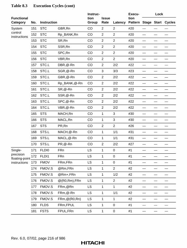
Rev. 6.0, 07/02, page 216 of 986
Table 8.3 Execution Cycles (cont)
LockFunctionalCategory No. Instruction
Instruc-tionGroup
IssueRate Latency
Execu-tionPattern Stage Start Cycles
151 STC GBR,Rn CO 2 2 #20 — — —
152 STC Rp_BANK,Rn CO 2 2 #20 — — —
153 STC SR,Rn CO 2 2 #20 — — —
154 STC SSR,Rn CO 2 2 #20 — — —
155 STC SPC,Rn CO 2 2 #20 — — —
156 STC VBR,Rn CO 2 2 #20 — — —
157 STC.L DBR,@-Rn CO 2 2/2 #22 — — —
158 STC.L SGR,@-Rn CO 3 3/3 #23 — — —
159 STC.L GBR,@-Rn CO 2 2/2 #22 — — —
160 STC.L Rp_BANK,@-Rn CO 2 2/2 #22 — — —
161 STC.L SR,@-Rn CO 2 2/2 #22 — — —
162 STC.L SSR,@-Rn CO 2 2/2 #22 — — —
163 STC.L SPC,@-Rn CO 2 2/2 #22 — — —
164 STC.L VBR,@-Rn CO 2 2/2 #22 — — —
165 STS MACH,Rn CO 1 3 #30 — — —
166 STS MACL,Rn CO 1 3 #30 — — —
167 STS PR,Rn CO 2 2 #26 — — —
168 STS.L MACH,@-Rn CO 1 1/1 #31 — — —
169 STS.L MACL,@-Rn CO 1 1/1 #31 — — —
Systemcontrolinstructions
170 STS.L PR,@-Rn CO 2 2/2 #27 — — —
171 FLDI0 FRn LS 1 0 #1 — — —
172 FLDI1 FRn LS 1 0 #1 — — —
173 FMOV FRm,FRn LS 1 0 #1 — — —
174 FMOV.S @Rm,FRn LS 1 2 #2 — — —
175 FMOV.S @Rm+,FRn LS 1 1/2 #2 — — —
176 FMOV.S @(R0,Rm),FRn LS 1 2 #2 — — —
177 FMOV.S FRm,@Rn LS 1 1 #2 — — —
178 FMOV.S FRm,@-Rn LS 1 1/1 #2 — — —
179 FMOV.S FRm,@(R0,Rn) LS 1 1 #2 — — —
180 FLDS FRm,FPUL LS 1 0 #1 — — —
Single-precisionfloating-pointinstructions
181 FSTS FPUL,FRn LS 1 0 #1 — — —

Rev. 6.0, 07/02, page 217 of 986
Table 8.3 Execution Cycles (cont)
LockFunctionalCategory No. Instruction
Instruc-tionGroup
IssueRate Latency
Execu-tionPattern Stage Start Cycles
182 FABS FRn LS 1 0 #1 — — —
183 FADD FRm,FRn FE 1 3/4 #36 — — —
184 FCMP/EQ FRm,FRn FE 1 2/4 #36 — — —
185 FCMP/GT FRm,FRn FE 1 2/4 #36 — — —
186 FDIV FRm,FRn FE 1 12/13 #37 F3 2 10
F1 11 1
187 FLOAT FPUL,FRn FE 1 3/4 #36 — — —
188 FMAC FR0,FRm,FRn FE 1 3/4 #36 — — —
189 FMUL FRm,FRn FE 1 3/4 #36 — — —
190 FNEG FRn LS 1 0 #1 — — —
191 FSQRT FRn FE 1 11/12 #37 F3 2 9
F1 10 1
192 FSUB FRm,FRn FE 1 3/4 #36 — — —
193 FTRC FRm,FPUL FE 1 3/4 #36 — — —
194 FMOV DRm,DRn LS 1 0 #1 — — —
195 FMOV @Rm,DRn LS 1 2 #2 — — —
196 FMOV @Rm+,DRn LS 1 1/2 #2 — — —
197 FMOV @(R0,Rm),DRn LS 1 2 #2 — — —
198 FMOV DRm,@Rn LS 1 1 #2 — — —
199 FMOV DRm,@-Rn LS 1 1/1 #2 — — —
Single-precisionfloating-pointinstructions
200 FMOV DRm,@(R0,Rn) LS 1 1 #2 — — —
201 FABS DRn LS 1 0 #1 — — —
202 FADD DRm,DRn FE 1 (7, 8)/9 #39 F1 2 6
203 FCMP/EQ DRm,DRn CO 2 3/5 #40 F1 2 2
204 FCMP/GT DRm,DRn CO 2 3/5 #40 F1 2 2
205 FCNVDS DRm,FPUL FE 1 4/5 #38 F1 2 2
206 FCNVSD FPUL,DRn FE 1 (3, 4)/5 #38 F1 2 2
F3 2 23
F1 22 3
207 FDIV DRm,DRn FE 1 (24, 25)/26
#41
F1 2 2
208 FLOAT FPUL,DRn FE 1 (3, 4)/5 #38 F1 2 2
Double-precisionfloating-pointinstructions
209 FMUL DRm,DRn FE 1 (7, 8)/9 #39 F1 2 6

Rev. 6.0, 07/02, page 218 of 986
Table 8.3 Execution Cycles (cont)
LockFunctionalCategory No. Instruction
Instruc-tionGroup
IssueRate Latency
Execu-tionPattern Stage Start Cycles
210 FNEG DRn LS 1 0 #1 — — —
F3 2 22
F1 21 3
211 FSQRT DRn FE 1 (23, 24)/25
#41
F1 2 2
212 FSUB DRm,DRn FE 1 (7, 8)/9 #39 F1 2 6
Double-precisionfloating-pointinstructions
213 FTRC DRm,FPUL FE 1 4/5 #38 F1 2 2
214 LDS Rm,FPUL LS 1 1 #1 — — —
215 LDS Rm,FPSCR CO 1 4 #32 F1 3 3
216 LDS.L @Rm+,FPUL CO 1 1/2 #2 — — —
217 LDS.L @Rm+,FPSCR CO 1 1/4 #33 F1 3 3
218 STS FPUL,Rn LS 1 3 #1 — — —
219 STS FPSCR,Rn CO 1 3 #1 — — —
220 STS.L FPUL,@-Rn CO 1 1/1 #2 — — —
FPU systemcontrolinstructions
221 STS.L FPSCR,@-Rn CO 1 1/1 #2 — — —
222 FMOV DRm,XDn LS 1 0 #1 — — —
223 FMOV XDm,DRn LS 1 0 #1 — — —
224 FMOV XDm,XDn LS 1 0 #1 — — —
225 FMOV @Rm,XDn LS 1 2 #2 — — —
226 FMOV @Rm+,XDn LS 1 1/2 #2 — — —
227 FMOV @(R0,Rm),XDn LS 1 2 #2 — — —
228 FMOV XDm,@Rn LS 1 1 #2 — — —
229 FMOV XDm,@-Rm LS 1 1/1 #2 — — —
230 FMOV XDm,@(R0,Rn) LS 1 1 #2 — — —
231 FIPR FVm,FVn FE 1 4/5 #42 F1 3 1
232 FRCHG FE 1 1/4 #36 — — —
233 FSCHG FE 1 1/4 #36 — — —
F0 2 4
Graphicsaccelerationinstructions
234 FTRV XMTRX,FVn FE 1 (5, 5, 6,7)/8
#43
F1 3 4
Notes: 1. See table 8.1 for the instruction groups.2. Latency “L1/L2...”: Latency corresponding to a write to each register, including
MACH/MACL/FPSCR.Example: MOV.B @Rm+, Rn “1/2”: The latency for Rm is 1 cycle, and the latency for
Rn is 2 cycles.3. Branch latency: Interval until the branch destination instruction is fetched

Rev. 6.0, 07/02, page 219 of 986
4. Conditional branch latency “2 (or 1)”: The latency is 2 for a nonzero displacement, and1 for a zero displacement.
5. Double-precision floating-point instruction latency “(L1, L2)/L3”: L1 is the latency for FR[n+1], L2 that for FR [n], and L3 that for FPSCR.
6. FTRV latency “(L1, L2, L3, L4)/L5”: L1 is the latency for FR [n], L2 that for FR [n+1], L3that for FR [n+2], L4 that for FR [n+3], and L5 that for FPSCR.
7. Latency “L1/L2/L3/L4” of MAC.L and MAC.W instructions: L1 is the latency for Rm, L2that for Rn, L3 that for MACH, and L4 that for MACL.
8. Latency “L1/L2” of MUL.L, MULS.W, MULU.W, DMULS.L, and DMULU.L instructions:L1 is the latency for MACH, and L2 that for MACL.
9. Execution pattern: The instruction execution pattern number (see figure 8.2)
10. Lock/stage: Stage locked by the instruction11. Lock/start: Locking start cycle; 1 is the first D-stage of the instruction.12. Lock/cycles: Number of cycles locked
Exceptions:1. When a floating-point computation instruction is followed by an FMOV store, an STS
FPUL, Rn instruction, or an STS.L FPUL, @-Rn instruction, the latency of the floating-point computation is decreased by 1 cycle.
2. When the preceding instruction loads the shift amount of the following SHAD/SHLD, thelatency of the load is increased by 1 cycle.
3. When an LS group instruction with a latency of less than 3 cycles is followed by adouble-precision floating-point instruction, FIPR, or FTRV, the latency of the firstinstruction is increased to 3 cycles.Example: In the case of FMOV FR4,FR0 and FIPR FV0,FV4, FIPR is stalled for 2
cycles.4. When MAC/MUL/DMUL is followed by an STS.L MAC, @-Rn instruction, the latency of
MAC/MUL/DMUL is 5 cycles.5. In the case of consecutive executions of MAC/MUL/DMUL, the latency is decreased to
2 cycles.6. When an LDS to MAC is followed by an STS.L MAC, @-Rn instruction, the latency of
the LDS to MAC is 4 cycles.7. When an LDS to MAC is followed by MAC/MUL/DMUL, the latency of the LDS to MAC
is 1 cycle.8. When an FSCHG or FRCHG instruction is followed by an LS group instruction that
reads or writes to a floating-point register, the aforementioned LS group instruction[s]cannot be executed in parallel.
9. When a single-precision FTRC instruction is followed by an “STS FPUL, Rn” instruction,the latency of the single-precision FTRC instruction is 1 cycle.

Rev. 6.0, 07/02, page 220 of 986

Rev. 6.0, 07/02, page 221 of 986
Section 9 Power-Down Modes
9.1 Overview
In the power-down modes, some of the on-chip peripheral modules and the CPU functions arehalted, enabling power consumption to be reduced.
9.1.1 Types of Power-Down Modes
The following power-down modes and functions are provided:
• Sleep mode
• Deep sleep mode
• Standby mode
• Hardware standby mode*
• Module standby function (TMU, RTC, SCI/SCIF, DMAC, SQ*, and UBC* on-chip peripheralmodules)
Note: * SH7750S, SH7750R only
Table 9.1 shows the conditions for entering these modes from the program execution state, thestatus of the CPU and peripheral modules in each mode, and the method of exiting each mode.

Rev. 6.0, 07/02, page 222 of 986
Table 9.1 Status of CPU and Peripheral Modules in Power-Down Modes
Status
Power-DownMode
EnteringConditions CPG CPU
On-ChipMemory
On-chipPeripheralModules Pins
ExternalMemory
ExitingMethod
Sleep SLEEPinstructionexecutedwhile STBYbit is 0 inSTBCR
Operating Halted(registersheld)
Held Operating Held Refreshing • Interrupt
• Reset
Deepsleep
SLEEPinstructionexecutedwhile STBYbit is 0 inSTBCR,and DSLPbit is 1 inSTBCR2
Operating Halted(registersheld)
Held Operating(DMAhalted)
Held Self-refreshing
• Interrupt
• Reset
Standby SLEEPinstructionexecutedwhile STBYbit is 1 inSTBCR
Halted Halted(registersheld)
Held Halted* Held Self-refreshing
• Interrupt
• Reset
Hardwarestandby(SH7750S,SH7750R)
Setting CApin low
Halted Halted Undefined Halted* Highimpedance
Undefined • Power-onreset
Modulestandby
SettingMSTP bitto 1 inSTBCR/STBCR2
Operating Operating Held Specifiedmoduleshalted*
Held Refreshing • ClearingMSTP bitto 0
• Reset
Note: * The RTC operates when the START bit in RCR2 is 1 (see section 11, Realtime Clock(RTC)).

Rev. 6.0, 07/02, page 223 of 986
9.1.2 Register Configuration
Table 9.2 shows the registers used for power-down mode control.
Table 9.2 Power-Down Mode Registers
Name Abbreviation R/W Initial Value P4 AddressArea 7Address
AccessSize
Standby controlregister
STBCR R/W H'00 H'FFC00004 H'1FC00004 8
Standby controlregister 2
STBCR2 R/W H'00 H'FFC00010 H'1FC00010 8
Clock stopregister 00*
CLKSTP00 R/W H'00000000 H'FE0A0000 H'1E0A0000 32
Clock releaseregister 00*
CLKSTPCLR00 W H'00000000 H'FE0A0008 H'1E0A0008 32
Note: * SH7750R only
9.1.3 Pin Configuration
Table 9.3 shows the pins used for power-down mode control.
Table 9.3 Power-Down Mode Pins
Pin Name Abbreviation I/O Function
Processor status 1
Processor status 0
STATUS1
STATUS0
Output Indicate the processor’s operating status.(STATUS1, STATUS0)
HH: ResetHL: Sleep modeLH: Standby modeLL: Normal operation
Hardware standbyrequest(SH7750S andSH7750R only)
CA Input Transits to hardware standby mode by alow-level input to the pin.
Notes: H: High level
L: Low level

Rev. 6.0, 07/02, page 224 of 986
9.2 Register Descriptions
9.2.1 Standby Control Register (STBCR)
The standby control register (STBCR) is an 8-bit readable/writable register that specifies thepower-down mode status. It is initialized to H'00 by a power-on reset via the RESET pin or due towatchdog timer overflow.
Bit: 7 6 5 4 3 2 1 0
STBY PHZ PPU MSTP4 MSTP3 MSTP2 MSTP1 MSTP0
Initial value: 0 0 0 0 0 0 0 0
R/W: R/W R/W R/W R/W R/W R/W R/W R/W
Bit 7—Standby (STBY): Specifies a transition to standby mode.
Bit 7: STBY Description
0 Transition to sleep mode on execution of SLEEP instruction (Initial value)
1 Transition to standby mode on execution of SLEEP instruction
Bit 6—Peripheral Module Pin High Impedance Control (PHZ): Controls the state ofperipheral module related pins in standby mode. When the PHZ bit is set to 1, peripheral modulerelated pins go to the high-impedance state in standby mode.
For the relevant pins, see section 9.2.2, Peripheral Module Pin High Impedance Control.
Bit 6: PHZ Description
0 Peripheral module related pins are in normal state (Initial value)
1 Peripheral module related pins go to high-impedance state
Bit 5—Peripheral Module Pin Pull-Up Control (PPU): Controls the state of peripheral modulerelated pins. When the PPU bit is cleared to 0, the pull-up resistor is turned on for peripheralmodule related pins in the input or high-impedance state.
For the relevant pins, see section 9.2.3, Peripheral Module Pin Pull-Up Control.
Bit 5: PPU Description
0 Peripheral module related pin pull-up resistors are on (Initial value)
1 Peripheral module related pin pull-up resistors are off
Bit 4—Module Stop 4 (MSTP4): Specifies stopping of the clock supply to the DMAC among theon-chip peripheral modules. The clock supply to the DMAC is stopped when the MSTP4 bit is set
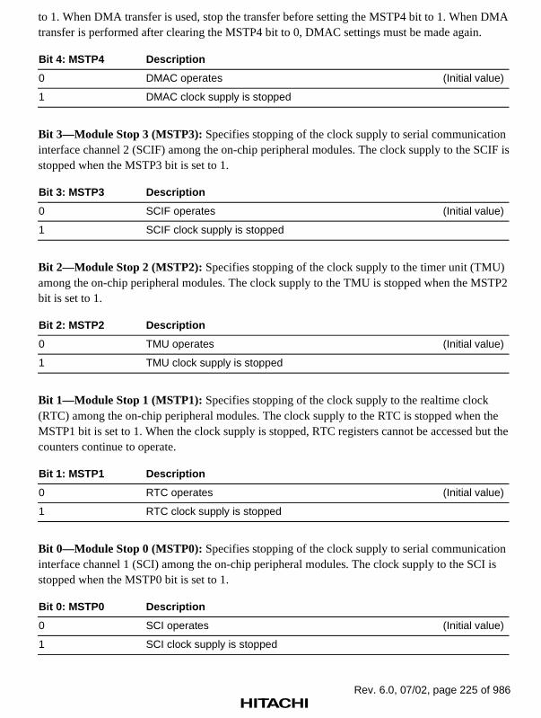
Rev. 6.0, 07/02, page 225 of 986
to 1. When DMA transfer is used, stop the transfer before setting the MSTP4 bit to 1. When DMAtransfer is performed after clearing the MSTP4 bit to 0, DMAC settings must be made again.
Bit 4: MSTP4 Description
0 DMAC operates (Initial value)
1 DMAC clock supply is stopped
Bit 3—Module Stop 3 (MSTP3): Specifies stopping of the clock supply to serial communicationinterface channel 2 (SCIF) among the on-chip peripheral modules. The clock supply to the SCIF isstopped when the MSTP3 bit is set to 1.
Bit 3: MSTP3 Description
0 SCIF operates (Initial value)
1 SCIF clock supply is stopped
Bit 2—Module Stop 2 (MSTP2): Specifies stopping of the clock supply to the timer unit (TMU)among the on-chip peripheral modules. The clock supply to the TMU is stopped when the MSTP2bit is set to 1.
Bit 2: MSTP2 Description
0 TMU operates (Initial value)
1 TMU clock supply is stopped
Bit 1—Module Stop 1 (MSTP1): Specifies stopping of the clock supply to the realtime clock(RTC) among the on-chip peripheral modules. The clock supply to the RTC is stopped when theMSTP1 bit is set to 1. When the clock supply is stopped, RTC registers cannot be accessed but thecounters continue to operate.
Bit 1: MSTP1 Description
0 RTC operates (Initial value)
1 RTC clock supply is stopped
Bit 0—Module Stop 0 (MSTP0): Specifies stopping of the clock supply to serial communicationinterface channel 1 (SCI) among the on-chip peripheral modules. The clock supply to the SCI isstopped when the MSTP0 bit is set to 1.
Bit 0: MSTP0 Description
0 SCI operates (Initial value)
1 SCI clock supply is stopped

Rev. 6.0, 07/02, page 226 of 986
9.2.2 Peripheral Module Pin High Impedance Control
When bit 6 in the standby control register (STBCR) is set to 1, peripheral module related pins goto the high-impedance state in standby mode.
• Relevant Pins
SCI related pins MD0/SCK MD1/TXD2
MD7/TXD MD8/RTS2
CTS2
DMA related pins DACK0 DRAK0
DACK1 DRAK1
• Other Information
The setting in this register is invalid when the above pins are used as port output pins.
For details of pin states, see Appendix E, Pin Functions.
9.2.3 Peripheral Module Pin Pull-Up Control
When bit 5 in the standby control register (STBCR) is cleared to 0, peripheral module related pinsare pulled up when in the input or high-impedance state.
• Relevant Pins
SCI related pins MD0/SCK MD1/TXD2 MD2/RXD2
MD7/TXD MD8/RTS2 SCK2/MRESET
RXD CTS2
DMA related pins DREQ0 DACK0 DRAK0
DREQ1 DACK1 DRAK1
TMU related pin TCLK
• Other Information
The setting in this register is invalid in the hardware standby mode.
For details of pin states, see Appendix E, Pin Functions.

Rev. 6.0, 07/02, page 227 of 986
9.2.4 Standby Control Register 2 (STBCR2)
Standby control register 2 (STBCR2) is an 8-bit readable/writable register that specifies the sleepmode and deep sleep mode transition conditions. It is initialized to H'00 by a power-on reset viathe RESET pin or due to watchdog timer overflow.
Bit: 7 6 5 4 3 2 1 0
DSLP STHZ*2 — — — — MSTP6*1 MSTP5*1
Initial value: 0 0 0 0 0 0 0 0
R/W: R/W R/W R R R R R/W R/W
Notes: *1 Reserved bit in the SH7750.*2 Reserved bit in the SH7750 and SH7750S.
Bit 7—Deep Sleep (DSLP): Specifies a transition to deep sleep mode
Bit 7: DSLP Description
0 Transition to sleep mode or standby mode on execution of SLEEPinstruction, according to setting of STBY bit in STBCR register (Initial value)
1 Transition to deep sleep mode on execution of SLEEP instruction*
Note: * When the STBY bit in the STBCR register is 0
Bit 6 (SH7750R Only)—STATUS Pin High-Impedance Control (STHZ): This bit selectswhether the STATUS0 and 1 pins are set to high-impedance when in hardware standby mode.
Bit 6: STHZ Description
0 Sets STATUS0, 1 pins to high-impedance when in hardware standby mode(Initial value)
1 Drives STATUS0, 1 pins to LH when in hardware standby mode
Bit 6 (SH7750 and SH7750S)—Reserved: Only 0 should only be written to these bits; operationcannot be guaranteed if 1 is written. These bits are always read as 0.
Bits 5 to 2—Reserved: Only 0 should only be written to these bits; operation cannot beguaranteed if 1 is written. These bits are always read as 0.
Bits 1 and 0 (SH7750)—Reserved: Only 0 should only be written to these bits; operation cannotbe guaranteed if 1 is written. These bits are always read as 0.

Rev. 6.0, 07/02, page 228 of 986
Bit 1 (SH7750S and SH7750R)—Module Stop 6 (MSTP6): Specifies that the clock supply tothe store queue (SQ) in the cache controller (CCN) is stopped. Setting the MSTP6 bit to 1 stopsthe clock supply to the SQ, and the SQ functions are therefore unavailable.
Bit 1: MSTP6 Description
0 SQ operating (Initial value)
1 Clock supply to SQ stopped
Bit 0 (SH7750S and SH7750R)—Module Stop 5 (MSTP5): Specifies stopping of the clocksupply to the user break controller (UBC) among the on-chip peripheral modules. See section20.6, User Break Controller Stop Functions for how to set the clock supply.
Bit 0: MSTP5 Description
0 UBC operating (Initial value)
1 Clock supply to UBC stopped
9.2.5 Clock-Stop Register 00 (CLKSTP00) (SH7750R Only)
Clock-stop register 00 (CLKSTP00) controls the operation clock for peripheral modules. Toresume supply of the clock signal, write a 1 to the corresponding bit in the CLKSTPCLR00register. Writing a 0 to the CLKSTP00 register does not affect the register’s value. TheCLKSTP00 register is a 32-bit register that can be read from or written to. It is initialized toH'0000 0000 by a power-on reset, but not by a manual reset or when the device enters standbymode.
Bit: 31 30 29 28 27 26 25 24 23 22 21 20 19 18 17 16
— — — — — — — — — — — — — — — —
Initial value: 0 0 0 0 0 0 0 0 0 0 0 0 0 0 0 0
R/W: R R R R R R R R R R R R R R R R
Bit: 15 14 13 12 11 10 9 8 7 6 5 4 3 2 1 0
— — — — — — — — — — — — — — CSTP1 CSTP0
Initial value: 0 0 0 0 0 0 0 0 0 0 0 0 0 0 0 0
R/W: R R R R R R R R R R R R R R R/W R/W
Bits 31 to 2—Reserved: Any data written to these bits should always be 0. These bits are alwaysread as 0.

Rev. 6.0, 07/02, page 229 of 986
Bit 1—Clock stop 1 (CSTP1): This bit specifies stopping of the peripheral clock supply tochannels 3 and 4 of the timer unit (TMU).
Bit 1: CSTP1 Description
0 Peripheral clock is supplied to TMU channels 3 and 4 (Initial value)
1 Peripheral clock supply to TMU channels 3 and 4 is stopped
Bit 0 Clock Stop 0 (CSTP0): Specifies stopping of the peripheral clock supply to the interruptcontroller (INTC). If this bit is set, INTC does not detect interrupts on the TMU’s channels 3 and4.
Bit 0: CSTP0 Description
0 INTC detects interrupts on channels 3 and 4 of the TMU (Initial value)
1 INTC does not detect interrupts on channels 3 and 4 of the TMU
9.2.6 Clock-Stop Clear Register 00 (CLKSTPCLR00) (SH7750R Only)
The clock-stop clear register 00 (CLKSTPCLR00) is a 32-bit write-only register that clears thecorresponding bits of the CLKSTP00 register.
Bit: 31 30 29 28 27 26 25 24 23 22 21 20 19 18 17 16
Initial value: 0 0 0 0 0 0 0 0 0 0 0 0 0 0 0 0
R/W: W W W W W W W W W W W W W W W W
Bit: 15 14 13 12 11 10 9 8 7 6 5 4 3 2 1 0
Initial value: 0 0 0 0 0 0 0 0 0 0 0 0 0 0 0 0
R/W: W W W W W W W W W W W W W W W W
Bits 31 to 0 Clock-Stop Clear: Specify whether or not to clear the corresponding bit of theclock-stop setting. See section 9.2.5, Clock-Stop Register 00 (LKSTP00) (SH7750R only), for thecorrespondence between the bits and the clocks that are stopped.
Bits 31 to 0 Description
0 Does not change the clock-stop setting for the corresponding clock
1 Clears the clock-stop setting for the corresponding clock

Rev. 6.0, 07/02, page 230 of 986
9.3 Sleep Mode
9.3.1 Transition to Sleep Mode
If a SLEEP instruction is executed when the STBY bit in STBCR is cleared to 0, the chip switchesfrom the program execution state to sleep mode. After execution of the SLEEP instruction, theCPU halts but its register contents are retained. The on-chip peripheral modules continue tooperate, and the clock continues to be output from the CKIO pin.
In sleep mode, a high-level signal is output at the STATUS1 pin, and a low-level signal at theSTATUS0 pin.
9.3.2 Exit from Sleep Mode
Sleep mode is exited by means of an interrupt (NMI, IRL, or on-chip peripheral module) or areset. In sleep mode, interrupts are accepted even if the BL bit in the SR register is 1. If necessary,SPC and SSR should be saved to the stack before executing the SLEEP instruction.
Exit by Interrupt: When an NMI, IRL, or on-chip peripheral module interrupt is generated, sleepmode is exited and interrupt exception handling is executed. The code corresponding to theinterrupt source is set in the INTEVT register.
Exit by Reset: Sleep mode is exited by means of a power-on or manual reset via the RESET pin,or a power-on or manual reset executed when the watchdog timer overflows.
9.4 Deep Sleep Mode
9.4.1 Transition to Deep Sleep Mode
If a SLEEP instruction is executed when the STBY bit in STBCR is cleared to 0 and the DSLP bitin STBCR2 is set to 1, the chip switches from the program execution state to deep sleep mode.After execution of the SLEEP instruction, the CPU halts but its register contents are retained.Except for the DMAC*, on-chip peripheral modules continue to operate. The clock continues tobe output to the CKIO pin, but all bus access (including auto refresh) stops. When using memorythat requires refreshing, set the self-refresh function prior to making the transition to deep sleepmode.
In deep sleep mode, a high-level signal is output at the STATUS1 pin, and a low-level signal atthe STATUS0 pin.
Note: * Terminate DMA transfers prior to making the transition to deep sleep mode. If you make atransition to deep sleep mode while DMA transfers are in progress, the results of thosetransfers cannot be guaranteed.

Rev. 6.0, 07/02, page 231 of 986
9.4.2 Exit from Deep Sleep Mode
As with sleep mode, deep sleep mode is exited by means of an interrupt (NMI, IRL, or on-chipperipheral module) or a reset.
9.5 Standby Mode
9.5.1 Transition to Standby Mode
If a SLEEP instruction is executed when the STBY bit in STBCR is set to 1, the chip switchesfrom the program execution state to standby mode. In standby mode, the on-chip peripheralmodules halt as well as the CPU. Clock output from the CKIO pin is also stopped.
The CPU and cache register contents are retained. Some on-chip peripheral module registers areinitialized. The state of the peripheral module registers in standby mode is shown in table 9.4.
Table 9.4 State of Registers in Standby Mode
Module Initialized RegistersRegisters That RetainTheir Contents
Interrupt controller — All registers
User break controller — All registers
Bus state controller — All registers
On-chip oscillation circuits — All registers
Timer unit TSTR register* All registers except TSTR
Realtime clock — All registers
Direct memory access controller — All registers
Serial communication interface See Appendix A, Address List See Appendix A, Address List
Notes: DMA transfer should be terminated before making a transition to standby mode. Transferresults are not guaranteed if standby mode is entered during transfer.* Not initialized when the realtime clock (RTC) is in use (see section 12, Timer Unit
(TMU)).
The procedure for a transition to standby mode is shown below.
1. Clear the TME bit in the WDT timer control register (WTCSR) to 0, and stop the WDT.
Set the initial value for the up-count in the WDT timer counter (WTCNT), and set the clock tobe used for the up-count in bits CKS2–CKS0 in the WTCSR register.
2. Set the STBY bit in the STBCR register to 1, then execute a SLEEP instruction.
3. When standby mode is entered and the chip’s internal clock stops, a low-level signal is outputat the STATUS1 pin, and a high-level signal at the STATUS0 pin.

Rev. 6.0, 07/02, page 232 of 986
9.5.2 Exit from Standby Mode
Standby mode is exited by means of an interrupt (NMI, IRL, or on-chip peripheral module) or areset via the RESET pin.
Exit by Interrupt: A hot start can be performed by means of the on-chip WDT. When an NMI,IRL*1, RTC, or GPIO*2 interrupt is detected, the WDT starts counting. After the count overflows,clocks are supplied to the entire chip, standby mode is exited, and the STATUS1 and STATUS0pins both go low. Interrupt exception handling is then executed, and the code corresponding to theinterrupt source is set in the INTEVT register. In standby mode, interrupts are accepted even if theBL bit in the SR register is 1, and so, if necessary, SPC and SSR should be saved to the stackbefore executing the SLEEP instruction.
The phase of the CKIO pin clock output may be unstable immediately after an interrupt isdetected, until standby mode is exited.
Notes: *1 Only when the RTC clock (32.768 kHz) is operating (see section 19.2.2, IRLInterrupts), standby mode can be exited by means of IRL3–IRL0 (when the IRL3–IRL0 level is higher than the SR register I3–I0 mask level).
*2 GPIO can be used to cancel standby mode when the RTC clock (32.768 kHz) isoperating (when the GPIO level is higher than the SR register I3–I0 mask level).
Exit by Reset: Standby mode is exited by means of a reset (power-on or manual) via the RESETpin. The RESET pin should be held low until clock oscillation stabilizes. The internal clockcontinues to be output at the CKIO pin.
9.5.3 Clock Pause Function
In standby mode, it is possible to stop or change the frequency of the clock input from the EXTALpin. This function is used as follows.
1. Enter standby mode following the transition procedure described above.
2. When standby mode is entered and the chip’s internal clock stops, a low-level signal is outputat the STATUS1 pin, and a high-level signal at the STATUS0 pin.
3. The input clock is stopped, or its frequency changed, after the STATUS1 pin goes low and theSTATUS0 pin high.
4. When the frequency is changed, input an NMI or IRL interrupt after the change. When theclock is stopped, input an NMI or IRL interrupt after applying the clock.
5. After the time set in the WDT, clock supply begins inside the chip, the STATUS1 andSTATUS0 pins both go low, and operation is resumed from interrupt exception handling.

Rev. 6.0, 07/02, page 233 of 986
9.6 Module Standby Function
9.6.1 Transition to Module Standby Function
Setting the MSTP6–MSTP0, CSTP1, and CSTP0 bits in the standby control register to 1 enablesthe clock supply to the corresponding on-chip peripheral modules to be halted. Use of thisfunction allows power consumption in sleep mode to be further reduced.
In the module standby state, the on-chip peripheral module external pins retain their states prior tohalting of the modules, and most registers retain their states prior to halting of the modules.

Rev. 6.0, 07/02, page 234 of 986
Bit Description
CSTP1*6 0 Peripheral clock is supplied to TMU channels 3 and 4
1 Peripheral clock supplied to TMU channels 3 and 4 is stopped
CSTP0*6 0 INTC detects interrupts on TMU channels 3 and 4
1 INTC does not detect interrupts on TMU channels 3 and 4
MSTP6*4 0 SQ operates
1 Clock supplied to SQ is stopped
MSTP5*4 0 UBC operates
1 Clock supplied to UBC is stopped*5
MSTP4 0 DMAC operates
1 Clock supplied to DMAC is stopped*3
MSTP3 0 SCIF operates
1 Clock supplied to SCIF is stopped
MSTP2 0 TMU operates
1 Clock supplied to TMU is stopped, and register is initialized*1
MSTP1 0 RTC operates
1 Clock supplied to RTC is stopped*2
MSTP0 0 SCI operates
1 Clock supplied to SCI is stopped
Notes: *1 The register initialized is the same as in standby mode, but initialization is notperformed if the RTC clock is not in use (see section 12, Timer Unit (TMU)).
*2 The counter operates when the START bit in RCR2 is 1 (see section 11, RealtimeClock (RTC)).
*3 Terminate DMA transfers prior to making the transition to module standby mode. If youmake a transition to module standby mode while DMA transfers are in progress, theresults of those transfers cannot be guaranteed.
*4 SH7750S, SH7750R only*5 For details, see section 20.6, User Break Controller Stop Functions.*6 SH7750R only
9.6.2 Exit from Module Standby Function
The module standby function is exited by clearing the MSTP6–MSTP0, CSTP1, and CSTP0 bitsto 0, or by a power-on reset via the RESET pin or a power-on reset caused by watchdog timeroverflow.

Rev. 6.0, 07/02, page 235 of 986
9.7 Hardware Standby Mode (SH7750S, SH7750R Only)
9.7.1 Transition to Hardware Standby Mode
Setting the CA pin level low effects a transition to hardware standby mode. In this mode, allmodules other than the RTC stop, as in the standby mode selected using the SLEEP command.
Hardware standby mode differs from standby mode as follows:
1. Interrupts and manual resets are not available;
2. All output pins other than the STATUS pin are in the high-impedance state and the pull-upresistance is off.
3. Even when no power is supplied to power pins other than the RTC power supply pin, the RTCcontinues to operate.
The status of the STATUS pin is determined by the STHZ bit of STBCR2. See appendix E, PinFunctions, for details of output pin states.
Operation when a low-level is input to the CA pin when in the standby mode depends on the CPGstatus, as follows:
1. In standby mode
The clock remains stopped and a transition is made to the hardware standby state.
2. When WDT is operating when standby mode is exited by interrupt
Standby mode is momentarily exited, the CPU restarts, and then a transition is made tohardware standby mode.
Note that the level of the CA pin must be kept low while in hardware standby mode.
9.7.2 Exit from Hardware Standby Mode
Hardware standby mode can only be exited by effecting a power-on reset.
Setting the CA pin level high after the RESET pin level has been set low and the SCK2 pin highstarts the clock to oscillate. The RESET pin level should be kept low until the clock has stabilized,then set high so that the CPU starts the power-on reset procedure.
Note that hardware standby mode cannot be exited using interrupts or a manual reset.
9.7.3 Usage Notes
The CA pin level must be kept high during the power-on oscillation settling period when the RTCpower supply is started (figure 9.15).

Rev. 6.0, 07/02, page 236 of 986
9.8 STATUS Pin Change Timing
The STATUS1 and STATUS0 pin change timing is shown below.
The meaning of the STATUS pin settings is as follows:
Reset: HH (STATUS1 high, STATUS0 high)Sleep: HL (STATUS1 high, STATUS0 low)Standby: LH (STATUS1 low, STATUS0 high)Normal: LL (STATUS1 low, STATUS0 low)
The meaning of the clock units is as follows:
Bcyc: Bus clock cyclePcyc: Peripheral clock cycle

Rev. 6.0, 07/02, page 237 of 986
9.8.1 In Reset
Power-On Reset
CKIO
STATUS
SCK2
Normal Reset Normal
0–5 Bcyc0–30 Bcyc
PLL stabilization time
Figure 9.1 STATUS Output in Power-On Reset
Manual Reset
CKIO
*
STATUS Normal Reset Normal
SCK2
0–30 Bcyc≥ 0 Bcyc
Note: * In a manual reset, STATUS = HH (reset) is set and an internal reset started after waiting until the end of the currently executing bus cycle.
Figure 9.2 STATUS Output in Manual Reset
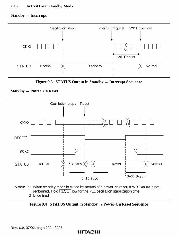
Rev. 6.0, 07/02, page 238 of 986
9.8.2 In Exit from Standby Mode
Standby →→→→ Interrupt
CKIO
STATUS Normal Standby Normal
WDT count
Oscillation stops Interrupt request WDT overflow
Figure 9.3 STATUS Output in Standby →→→→ Interrupt Sequence
Standby →→→→ Power-On Reset
Reset
CKIO
*1
STATUS Normal Reset Normal
0–10 Bcyc
Standby
Oscillation stops
SCK2
*2
0–30 Bcyc
Notes: *1 When standby mode is exited by means of a power-on reset, a WDT count is not performed. Hold low for the PLL oscillation stabilization time.
*2 Undefined
Figure 9.4 STATUS Output in Standby →→→→ Power-On Reset Sequence

Rev. 6.0, 07/02, page 239 of 986
Standby →→→→ Manual Reset
Reset
CKIO
*1
STATUS Normal Reset Normal
0–10 Bcyc
Standby
Oscillation stops
SCK2
*2
0–30 Bcyc
Notes: *1 When standby mode is exited by means of a manual reset, a WDT count is not performed. Hold low for the PLL oscillation stabilization time.
*2 Undefined
Figure 9.5 STATUS Output in Standby →→→→ Manual Reset Sequence

Rev. 6.0, 07/02, page 240 of 986
9.8.3 In Exit from Sleep Mode
Sleep →→→→ Interrupt
CKIO
STATUS Normal Sleep Normal
Interrupt request
Figure 9.6 STATUS Output in Sleep →→→→ Interrupt Sequence
Sleep →→→→ Power-On Reset
Reset
CKIO
STATUS Normal ResetSleep Normal
0–10 Bcyc0–30 Bcyc
*1
SCK2
*2
Notes: *1 When sleep mode is exited by means of a power-on reset, hold low for the oscillation stabilization time.
*2 Undefined
Figure 9.7 STATUS Output in Sleep →→→→ Power-On Reset Sequence

Rev. 6.0, 07/02, page 241 of 986
Sleep →→→→ Manual Reset
Reset
*
STATUS Normal ResetSleep Normal
CKIO
0–30 Bcyc 0–30 Bcyc
Note: * Hold low until STATUS = reset.
SCK2
Figure 9.8 STATUS Output in Sleep →→→→ Manual Reset Sequence
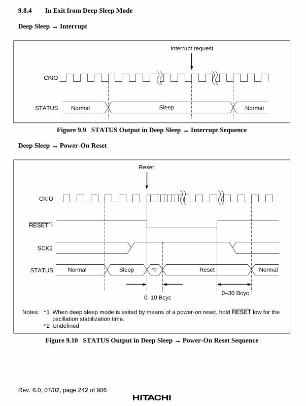
Rev. 6.0, 07/02, page 242 of 986
9.8.4 In Exit from Deep Sleep Mode
Deep Sleep →→→→ Interrupt
CKIO
STATUS Normal Sleep Normal
Interrupt request
Figure 9.9 STATUS Output in Deep Sleep →→→→ Interrupt Sequence
Deep Sleep →→→→ Power-On Reset
Reset
CKIO
STATUS Normal Sleep Reset Normal
0–10 Bcyc0–30 Bcyc
*1
SCK2
*2
Notes: *1 When deep sleep mode is exited by means of a power-on reset, hold low for the oscillation stabilization time.
*2 Undefined
Figure 9.10 STATUS Output in Deep Sleep →→→→ Power-On Reset Sequence
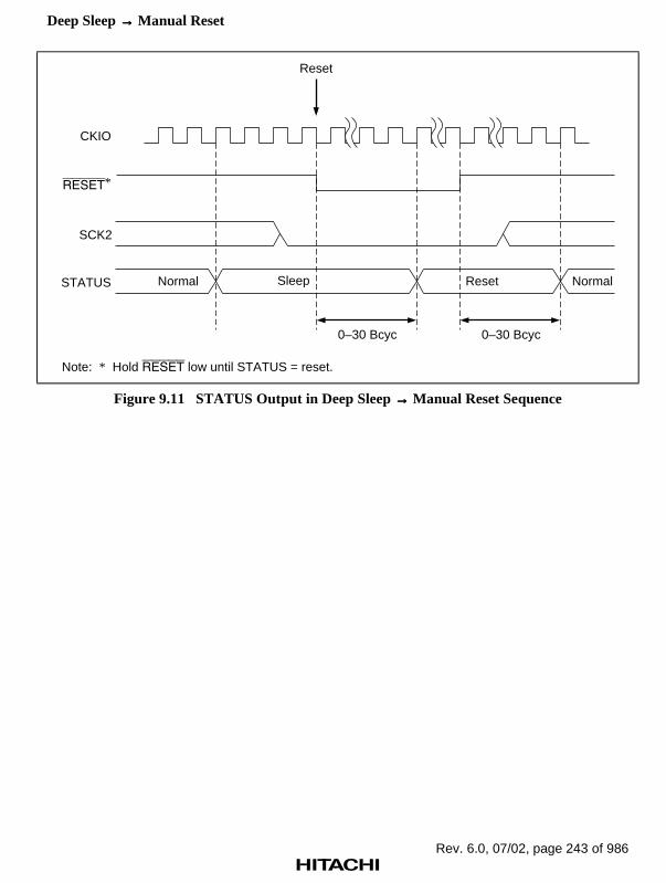
Rev. 6.0, 07/02, page 243 of 986
Deep Sleep →→→→ Manual Reset
Reset
*
STATUS Normal Sleep Reset Normal
CKIO
0–30 Bcyc 0–30 Bcyc
Note: * Hold low until STATUS = reset.
SCK2
Figure 9.11 STATUS Output in Deep Sleep →→→→ Manual Reset Sequence

Rev. 6.0, 07/02, page 244 of 986
9.8.5 Hardware Standby Mode Timing (SH7750S, SH7750R Only)
Figure 9.12 shows the timing of the signals of the respective pins in hardware standby mode.
The CA pin level must be kept low while in hardware standby mode.
After setting the RESET pin level low, the clock starts when the CA pin level is switched to high.
CKIO
CA
SCK2 (High)
STATUS Reset
0–10 Bcyc0–10 Bcyc
Waiting for end of bus cycle
*2
Notes: *1 Same at sleep and reset.*2 Undefined*3 High impedance when STBCR2. STHZ = 0
Normal*1 Standby*3
Figure 9.12 Hardware Standby Mode Timing(When CA = Low in Normal Operation)

Rev. 6.0, 07/02, page 245 of 986
CKIO
(High)
CA
STATUS Standby
0–10 Bcyc
Normal
(High)SCK2
WDT count
WDT overflowInterrupt request
Note: * High impedance when STBCR2. STHZ = 0
Standby*
Figure 9.13 Hardware Standby Mode Timing(When CA = Low in WDT Operation)

Rev. 6.0, 07/02, page 246 of 986
VDDQ*
VDD
SCK2
CA
Min 0s
Min 0s
Max 50 µs
Note: * VDDQ, VDD-CPG, VDD-PLL1, VDD-PLL2
VDD min
Figure 9.14 Timing When Power Other than VDD-RTC is Off
CA
VDD-RTC
SCK2
VDD, VDDQ*
Min 0s
Note: * VDD, VDD-PLL1/2, VDDQ, VDD-CPG
Power-on oscillationsetting time
Figure 9.15 Timing When VDD-RTC Power is Off →→→→ On

Rev. 6.0, 07/02, page 247 of 986
Section 10 Clock Oscillation Circuits
10.1 Overview
The on-chip oscillation circuits comprise a clock pulse generator (CPG) and a watchdog timer(WDT).
The CPG generates the clocks supplied inside the processor and performs power-down modecontrol.
The WDT is a single-channel timer used to count the clock stabilization time when exiting standbymode or the frequency is changed. It can be used as a normal watchdog timer or an interval timer.
10.1.1 Features
The CPG has the following features:
• Three clocks
The CPG can generate independently the CPU clock (Iφ) used by the CPU, FPU, caches, andTLB, the peripheral module clock (Pφ) used by the peripheral modules, and the bus clock(CKIO) used by the external bus interface.
• Six clock modes
Any of six clock operating modes can be selected, with different combinations of CPU clock,bus clock, and peripheral module clock division ratios after a power-on reset.
• Frequency change function
PLL (phase-locked loop) circuits and a frequency divider in the CPG enable the CPU clock,bus clock, and peripheral module clock frequencies to be changed independently. Frequencychanges are performed by software in accordance with the settings in the frequency controlregister (FRQCR).
• PLL on/off control
Power consumption can be reduced by stopping the PLL circuits during low-frequencyoperation.
• Power-down mode control
It is possible to stop the clock in sleep mode and standby mode, and to stop specific moduleswith the module standby function.

Rev. 6.0, 07/02, page 248 of 986
The WDT has the following features
• Can be used to secure clock stabilization time
Used when exiting standby mode or a temporary standby state when the clock frequency ischanged.
• Can be switched between watchdog timer mode and interval timer mode
• Internal reset generation in watchdog timer mode
An internal reset is executed on counter overflow.
Power-on reset or manual reset can be selected.
• Interrupt generation in interval timer mode
An interval timer interrupt is generated on counter overflow.
• Selection of eight counter input clocks
Any of eight clocks can be selected, scaled from the ×1 clock of frequency divider 2 shown infigure 10.1.
The CPG is described in sections 10.2 to 10.6, and the WDT in sections 10.7 to 10.9.

Rev. 6.0, 07/02, page 249 of 986
10.2 Overview of CPG
10.2.1 Block Diagram of CPG
Figure 10.1 (1) shows a block diagram of the CPG in the SH7750 and SH7750S, and figure 10.1(2) a block diagram of the CPG in the SH7750R.
FRQCR: Frequency control registerSTBCR: Standby control registerSTBCR2: Standby control register 2
Oscillator circuit
PLL circuit 1
Frequency divider 2
Crystaloscillator
Frequencydivider 1
PLL circuit 2
CPU clock (Iø) cycle Icyc
Peripheral module clock (Pø) cycle Pcyc
Bus clock (Bø) cycle Bcyc
CPG control unit
Clock frequencycontrol circuit
Standby controlcircuit
Bus interface
Internal bus
XTAL
EXTAL
MD8
CKIO
MD2MD1MD0
FRQCRSTBCR2
× 1× 1/2× 1/3× 1/4× 1/6× 1/8
× 6
× 1/2
× 1
STBCR
Figure 10.1 (1) Block Diagram of CPG (SH7750, SH7750S)

Rev. 6.0, 07/02, page 250 of 986
FRQCR: STBCR:STBCR2:
Frequency control registerStandby control registerStandby control register 2
Oscillator circuit
PLL circuit 1
Frequencydivider 2
Crystaloscillator
CPU clock (Iø)cycle Icyc
Peripheral moduleclock (Pø) cyclePcyc
Bus clock (Bø)cycle Bcyc
CPG control unit
Clock frequencycontrol circuit
Standby controlcircuit
Bus interface
Internal bus
XTAL
EXTAL
MD8
CKIO
MD2MD1MD0
FRQCR
STBCR2
× 1× 1/2× 1/3× 1/4× 1/6× 1/8
× 6× 12
PLL circuit 2
× 1
STBCR
Figure 10.1 (2) Block Diagram of CPG (SH7750R)

Rev. 6.0, 07/02, page 251 of 986
The function of each of the CPG blocks is described below.
PLL Circuit 1: PLL circuit 1 has a function for multiplying the clock frequency from the EXTALpin or crystal oscillator by 6 with the SH7750 and SH7750S, and by 6 or 12 with the SH7750R.Starting and stopping is controlled by a frequency control register setting. Control is performed sothat the internal clock rising edge phase matches the input clock rising edge phase.
PLL Circuit 2: PLL circuit 2 coordinates the phases of the bus clock and the CKIO pin outputclock. Starting and stopping is controlled by a frequency control register setting.
Crystal Oscillator: This is the oscillator circuit used when a crystal resonator is connected to theXTAL and EXTAL pins. Use of the crystal oscillator can be selected with the MD8 pin.
Frequency Divider 1 (SH7750 and SH7750S only): Frequency divider 1 has a function foradjusting the clock waveform duty to 50% by halving the input clock frequency when clock inputfrom the EXTAL pin is supplied internally without using PLL circuit 1.
Frequency Divider 2: Frequency divider 2 generates the CPU clock (Iφ), bus clock (Bφ), andperipheral module clock (Pφ). The division ratio is set in the frequency control register.
Clock Frequency Control Circuit: The clock frequency control circuit controls the clockfrequency by means of the MD pins and frequency control register.
Standby Control Circuit: The standby control circuit controls the state of the on-chip oscillationcircuits and other modules when the clock is switched and in sleep and standby modes.
Frequency Control Register (FRQCR): The frequency control register contains control bits forclock output from the CKIO pin, PLL circuit 1 and 2 on/off control, and the CPU clock, bus clock,and peripheral module clock frequency division ratios.
Standby Control Register (STBCR): The standby control register contains power save modecontrol bits. For further information on the standby control register, see section 9, Power-DownModes.
Standby Control Register 2 (STBCR2): Standby control register 2 contains a power save modecontrol bit. For further information on standby control register 2, see section 9, Power-DownModes.

Rev. 6.0, 07/02, page 252 of 986
10.2.2 CPG Pin Configuration
Table 10.1 shows the CPG pins and their functions.
Table 10.1 CPG Pins
Pin Name Abbreviation I/O Function
Mode control pins MD0 Input Set clock operating mode
MD1
MD2
XTAL Output Connects crystal resonator
EXTAL Input Connects crystal resonator, or used asexternal clock input pin
Crystal I/O pins(clock input pins)
MD8 Input Selects use/non-use of crystal resonator
When MD8 = 0, external clock is input fromEXTAL
When MD8 = 1, crystal resonator isconnected directly to EXTAL and XTAL
Clock output pin CKIO Output Used as external clock output pin
Level can also be fixed
CKIO enable pin CKE Output 0 when CKIO output clock is unstable and incase of synchronous DRAM self-refreshing*
Note: * Set to 1 in a power-on reset.For details of synchronous DRAM self-refreshing, see section 13.3.5, Synchronous DRAMInterface.
10.2.3 CPG Register Configuration
Table 10.2 shows the CPG register configuration.
Table 10.2 CPG Register
Name Abbreviation R/W Initial Value P4 AddressArea 7Address
AccessSize
Frequency controlregister
FRQCR R/W Undefined* H'FFC00000 H'1FC00000 16
Note: * Depends on the clock operating mode set by pins MD2–MD0.
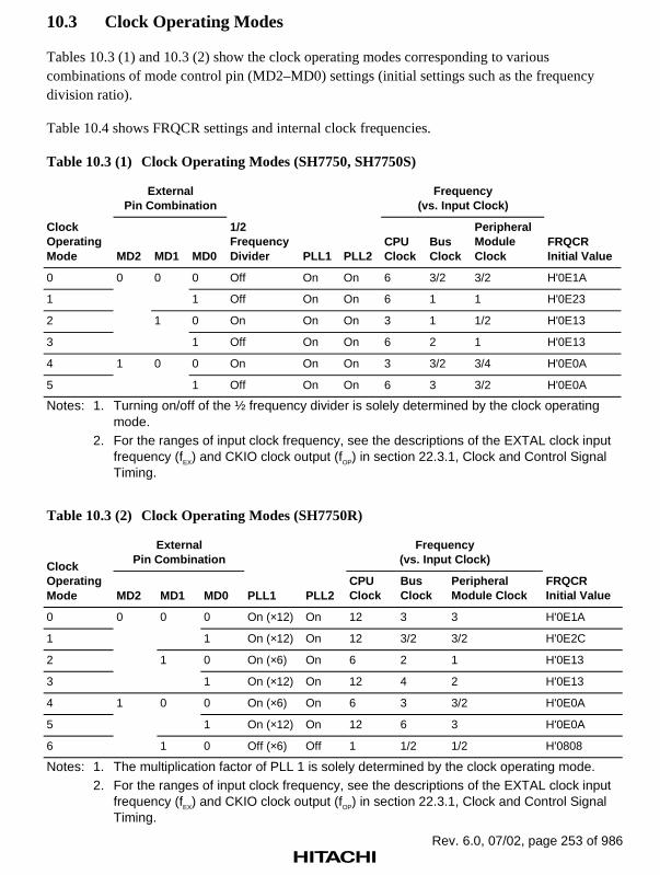
Rev. 6.0, 07/02, page 253 of 986
10.3 Clock Operating Modes
Tables 10.3 (1) and 10.3 (2) show the clock operating modes corresponding to variouscombinations of mode control pin (MD2–MD0) settings (initial settings such as the frequencydivision ratio).
Table 10.4 shows FRQCR settings and internal clock frequencies.
Table 10.3 (1) Clock Operating Modes (SH7750, SH7750S)
ExternalPin Combination
Frequency(vs. Input Clock)
ClockOperatingMode MD2 MD1 MD0
1/2FrequencyDivider PLL1 PLL2
CPUClock
BusClock
PeripheralModuleClock
FRQCRInitial Value
0 0 Off On On 6 3/2 3/2 H'0E1A
1
0
1 Off On On 6 1 1 H'0E23
2 0 On On On 3 1 1/2 H'0E13
3
0
1
1 Off On On 6 2 1 H'0E13
4 0 On On On 3 3/2 3/4 H'0E0A
5
1 0
1 Off On On 6 3 3/2 H'0E0A
Notes: 1. Turning on/off of the ½ frequency divider is solely determined by the clock operatingmode.
2. For the ranges of input clock frequency, see the descriptions of the EXTAL clock inputfrequency (fEX) and CKIO clock output (fOP) in section 22.3.1, Clock and Control SignalTiming.
Table 10.3 (2) Clock Operating Modes (SH7750R)
ExternalPin Combination
Frequency(vs. Input Clock)
ClockOperatingMode MD2 MD1 MD0 PLL1 PLL2
CPUClock
BusClock
PeripheralModule Clock
FRQCRInitial Value
0 0 On (×12) On 12 3 3 H'0E1A
1
0
1 On (×12) On 12 3/2 3/2 H'0E2C
2 0 On (×6) On 6 2 1 H'0E13
3
0
1
1 On (×12) On 12 4 2 H'0E13
4 0 On (×6) On 6 3 3/2 H'0E0A
5
0
1 On (×12) On 12 6 3 H'0E0A
6
1
1 0 Off (×6) Off 1 1/2 1/2 H'0808
Notes: 1. The multiplication factor of PLL 1 is solely determined by the clock operating mode.2. For the ranges of input clock frequency, see the descriptions of the EXTAL clock input
frequency (fEX) and CKIO clock output (fOP) in section 22.3.1, Clock and Control SignalTiming.

Rev. 6.0, 07/02, page 254 of 986
Table 10.4 FRQCR Settings and Internal Clock Frequencies
Frequency Division RatioFRQCR(Lower 9 Bits) CPU Clock Bus Clock Peripheral Module Clock
H'008 1/2
H'00A 1/4
H'00C
1/2
1/8
H'011 1/3
H'013
1/3
1/6
H'01A 1/4
H'01C
1/4
1/8
H'023 1/6 1/6
H'02C
1
1/8 1/8
H'05A 1/4
H'05C
1/4
1/8
H'063 1/6 1/6
H'06C
1/2
1/8 1/8
H'0A3 1/3 1/6 1/6
H'0EC 1/4 1/8 1/8
Note: For the lower 9 bits of FRQCR, do not set values other than those shown in the table.
10.4 CPG Register Description
10.4.1 Frequency Control Register (FRQCR)
The frequency control register (FRQCR) is a 16-bit readable/writable register that specifiesuse/non-use of clock output from the CKIO pin, PLL circuit 1 and 2 on/off control, and the CPUclock, bus clock, and peripheral module clock frequency division ratios. Only word access can beused on FRQCR.
FRQCR is initialized only by a power-on reset via the RESET pin. The initial value of each bit isdetermined by the clock operating mode.

Rev. 6.0, 07/02, page 255 of 986
Bit: 15 14 13 12 11 10 9 8
— — — — CKOEN PLL1EN PLL2EN IFC2
Initial value: 0 0 0 0 1 1 1 —
R/W: R/W R/W R/W R R/W R/W R/W R/W
Bit: 7 6 5 4 3 2 1 0
IFC1 IFC0 BFC2 BFC1 BFC0 PFC2 PFC1 PFC0
Initial value: — — — — — — — —
R/W: R/W R/W R/W R/W R/W R/W R/W R/W
Bits 15 to 12—Reserved: These bits are always read as 0, and should only be written with 0.
Bit 11—Clock Output Enable (CKOEN): Specifies whether a clock is output from the CKIOpin or the CKIO pin is placed in the high-impedance state. When the CKIO pin goes to the high-impedance state, operation continues at the operating frequency before this state was entered.When the CKIO pin becomes high-impedance, it is pulled up.
Bit 11: CKOEN Description
0 CKIO pin goes to high-impedance state (pulled up*)
1 Clock is output from CKIO pin (Initial value)
Note: * It is not pulled up in hardware standby mode.
Bit 10—PLL Circuit 1 Enable (PLL1EN): Specifies whether PLL circuit 1 is on or off.
Bit 10: PLL1EN Description
0 PLL circuit 1 is not used
1 PLL circuit 1 is used (Initial value)
Bit 9—PLL Circuit 2 Enable (PLL2EN): Specifies whether PLL circuit 2 is on or off.
Bit 9: PLL2EN Description
0 PLL circuit 2 is not used
1 PLL circuit 2 is used (Initial value)
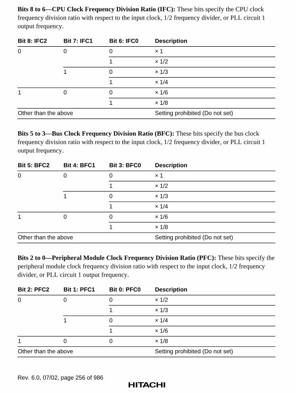
Rev. 6.0, 07/02, page 256 of 986
Bits 8 to 6—CPU Clock Frequency Division Ratio (IFC): These bits specify the CPU clockfrequency division ratio with respect to the input clock, 1/2 frequency divider, or PLL circuit 1output frequency.
Bit 8: IFC2 Bit 7: IFC1 Bit 6: IFC0 Description
0 0 0 × 1
1 × 1/2
1 0 × 1/3
1 × 1/4
1 0 0 × 1/6
1 × 1/8
Other than the above Setting prohibited (Do not set)
Bits 5 to 3—Bus Clock Frequency Division Ratio (BFC): These bits specify the bus clockfrequency division ratio with respect to the input clock, 1/2 frequency divider, or PLL circuit 1output frequency.
Bit 5: BFC2 Bit 4: BFC1 Bit 3: BFC0 Description
0 0 0 × 1
1 × 1/2
1 0 × 1/3
1 × 1/4
1 0 0 × 1/6
1 × 1/8
Other than the above Setting prohibited (Do not set)
Bits 2 to 0—Peripheral Module Clock Frequency Division Ratio (PFC): These bits specify theperipheral module clock frequency division ratio with respect to the input clock, 1/2 frequencydivider, or PLL circuit 1 output frequency.
Bit 2: PFC2 Bit 1: PFC1 Bit 0: PFC0 Description
0 0 0 × 1/2
1 × 1/3
1 0 × 1/4
1 × 1/6
1 0 0 × 1/8
Other than the above Setting prohibited (Do not set)

Rev. 6.0, 07/02, page 257 of 986
10.5 Changing the Frequency
There are two methods of changing the internal clock frequency: by changing stopping andstarting of PLL circuit 1, and by changing the frequency division ratio of each clock. In bothcases, control is performed by software by means of the frequency control register. These methodsare described below.
10.5.1 Changing PLL Circuit 1 Starting/Stopping (When PLL Circuit 2 is Off)
When PLL circuit 1 is changed from the stopped to started state, a PLL stabilization time isrequired. The oscillation stabilization time count is performed by the on-chip WDT.
1. Set a value in WDT to provide the specified oscillation stabilization time, and stop the WDT.The following settings are necessary:
WTCSR register TME bit = 0: WDT stopped
WTCSR register CKS2–CKS0 bits: WDT count clock division ratio
WTCNT counter: Initial counter value
2. Set the PLL1EN bit to 1.
3. Internal processor operation stops temporarily, and the WDT starts counting up. The internalclock stops and an unstable clock is output to the CKIO pin.
4. After the WDT count overflows, clock supply begins within the chip and the processorresumes operation. The WDT stops after overflowing.
10.5.2 Changing PLL Circuit 1 Starting/Stopping (When PLL Circuit 2 is On)
When PLL circuit 2 is on, a PLL circuit 1 and PLL circuit 2 oscillation stabilization time isrequired.
1. Make WDT settings as in 10.5.1.
2. Set the PLL1EN bit to 1.
3. Internal processor operation stops temporarily, PLL circuit 1 oscillates, and the WDT startscounting up. The internal clock stops and an unstable clock is output to the CKIO pin.
4. After the WDT count overflows, PLL circuit 2 starts oscillating. The WDT resumes its up-count from the value set in step 1 above. During this time, also, the internal clock is stoppedand an unstable clock is output to the CKIO pin.
5. After the WDT count overflows, clock supply begins within the chip and the processorresumes operation. The WDT stops after overflowing.

Rev. 6.0, 07/02, page 258 of 986
10.5.3 Changing Bus Clock Division Ratio (When PLL Circuit 2 is On)
If PLL circuit 2 is on when the bus clock frequency division ratio is changed, a PLL circuit 2oscillation stabilization time is required.
1. Make WDT settings as in 10.5.1.
2. Set the BFC2–BFC0 bits to the desired value.
3. Internal processor operation stops temporarily, and the WDT starts counting up. The internalclock stops and an unstable clock is output to the CKIO pin.
4. After the WDT count overflows, clock supply begins within the chip and the processorresumes operation. The WDT stops after overflowing.
10.5.4 Changing Bus Clock Division Ratio (When PLL Circuit 2 is Off)
If PLL circuit 2 is off when the bus clock frequency division ratio is changed, a WDT count is notperformed.
1. Set the BFC2–BFC0 bits to the desired value.
2. The set clock is switched to immediately.
10.5.5 Changing CPU or Peripheral Module Clock Division Ratio
When the CPU or peripheral module clock frequency division ratio is changed, a WDT count isnot performed.
1. Set the IFC2–IFC0 or PFC2–PFC0 bits to the desired value.
2. The set clock is switched to immediately.
10.6 Output Clock Control
The CKIO pin can be switched between clock output and a fixed level setting by means of theCKOEN bit in the FRQCR register. When the CKIO pin goes to the high-impedance state, it ispulled up.

Rev. 6.0, 07/02, page 259 of 986
10.7 Overview of Watchdog Timer
10.7.1 Block Diagram
Figure 10.2 shows a block diagram of the WDT.
Standby release
Internal reset request
Interrupt request
Standbycontrol
Resetcontrol
Interruptcontrol
WTCSR WTCNT
Bus interface
Clock selection
Overflow
Frequency divider
Clock selector
Clock
WDT
WTCSR: Watchdog timer control/status registerWTCNT: Watchdog timer counter
Standby mode
Frequency divider 2 ×1 clock
Figure 10.2 Block Diagram of WDT

Rev. 6.0, 07/02, page 260 of 986
10.7.2 Register Configuration
The WDT has the two registers summarized in table 10.5. These registers control clock selectionand timer mode switching.
Table 10.5 WDT Registers
Name Abbreviation R/WInitialValue P4 Address
Area 7Address Access Size
Watchdog timercounter
WTCNT R/W* H'00 H'FFC00008 H'1FC00008 R: 8, W: 16*
Watchdog timercontrol/statusregister
WTCSR R/W* H'00 H'FFC0000C H'1FC0000C R: 8, W: 16*
Note: * Use word-size access when writing. Perform the write with the upper byte set to H'5A orH'A5, respectively. Byte- and longword-size writes cannot be used.Use byte access when reading.
10.8 WDT Register Descriptions
10.8.1 Watchdog Timer Counter (WTCNT)
The watchdog timer counter (WTCNT) is an 8-bit readable/writable counter that counts up on theselected clock. When WTCNT overflows, a reset is generated in watchdog timer mode, or aninterrupt in interval timer mode. WTCNT is initialized to H'00 only by a power-on reset via theRESET pin.
To write to the WTCNT counter, use a word-size access with the upper byte set to H'5A. To readWTCNT, use a byte-size access.
Bit: 7 6 5 4 3 2 1 0
Initial value: 0 0 0 0 0 0 0 0
R/W: R/W R/W R/W R/W R/W R/W R/W R/W

Rev. 6.0, 07/02, page 261 of 986
10.8.2 Watchdog Timer Control/Status Register (WTCSR)
The watchdog timer control/status register (WTCSR) is an 8-bit readable/writable registercontaining bits for selecting the count clock and timer mode, and overflow flags.
WTCSR is initialized to H'00 only by a power-on reset via the RESET pin. It retains its value inan internal reset due to WDT overflow. When used to count the clock stabilization time whenexiting standby mode, WTCSR retains its value after the counter overflows.
To write to the WTCSR register, use a word-size access with the upper byte set to H'A5. To readWTCSR, use a byte-size access.
Bit: 7 6 5 4 3 2 1 0
TME WT/IT RSTS WOVF IOVF CKS2 CKS1 CKS0
Initial value: 0 0 0 0 0 0 0 0
R/W: R/W R/W R/W R/W R/W R/W R/W R/W
Bit 7—Timer Enable (TME): Specifies starting and stopping of timer operation. Clear this bit to0 when using the WDT in standby mode or to change a clock frequency.
Bit 7: TME Description
0 Up-count stopped, WTCNT value retained (Initial value)
1 Up-count started
Bit 6—Timer Mode Select (WT/ITITITIT): Specifies whether the WDT is used as a watchdog timer orinterval timer.
Bit 6: WT/ITITITIT Description
0 Interval timer mode (Initial value)
1 Watchdog timer mode
Note: The up-count may not be performed correctly if WT/IT is modified while the WDT is running.
Bit 5—Reset Select (RSTS): Specifies the kind of reset to be performed when WTCNToverflows in watchdog timer mode. This setting is ignored in interval timer mode.
Bit 5: RSTS Description
0 Power-on reset (Initial value)
1 Manual reset

Rev. 6.0, 07/02, page 262 of 986
Bit 4—Watchdog Timer Overflow Flag (WOVF): Indicates that WTCNT has overflowed inwatchdog timer mode. This flag is not set in interval timer mode.
Bit 4: WOVF Description
0 No overflow (Initial value)
1 WTCNT has overflowed in watchdog timer mode
Bit 3—Interval Timer Overflow Flag (IOVF): Indicates that WTCNT has overflowed ininterval timer mode. This flag is not set in watchdog timer mode.
Bit 3: IOVF Description
0 No overflow (Initial value)
1 WTCNT has overflowed in interval timer mode
Bits 2 to 0—Clock Select 2 to 0 (CKS2–CKS0): These bits select the clock used for the WTCNTcount from eight clocks obtained by dividing the frequency divider 2 input clock*. The overflowperiods shown in the following table are for use of a 33 MHz input clock, with frequency divider 1off, and PLL circuit 1 on (×6).
Note: * When PLL1 is switched on or off, the clock following the switch is used.
Description
Bit 2: CKS2 Bit 1: CKS1 Bit 0: CKS0 Clock Division Ratio Overflow Period
0 0 0 1/32 (Initial value) 41 µs
1 1/64 82 µs
1 0 1/128 164 µs
1 1/256 328 µs
1 0 0 1/512 656 µs
1 1/1024 1.31 ms
1 0 1/2048 2.62 ms
1 1/4096 5.25 ms
Note: The up-count may not be performed correctly if bits CKS2–CKS0 are modified while theWDT is running. Always stop the WDT before modifying these bits.

Rev. 6.0, 07/02, page 263 of 986
10.8.3 Notes on Register Access
The watchdog timer counter (WTCNT) and watchdog timer control/status register (WTCSR)differ from other registers in being more difficult to write to. The procedure for writing to theseregisters is given below.
Writing to WTCNT and WTCSR: These registers must be written to with a word transferinstruction. They cannot be written to with a byte or longword transfer instruction. When writingto WTCNT, perform the transfer with the upper byte set to H'5A and the lower byte containing thewrite data. When writing to WTCSR, perform the transfer with the upper byte set to H'A5 and thelower byte containing the write data. This transfer procedure writes the lower byte data toWTCNT or WTCSR. The write formats are shown in figure 10.3.
15 8 7 0
H'5A Write dataAddress: H'FFC00008 (H'1FC00008)
15 8 7 0
H'A5 Write dataAddress: H'FFC0000C (H'1FC0000C)
WTCSR write
WTCNT write
Figure 10.3 Writing to WTCNT and WTCSR
10.9 Using the WDT
10.9.1 Standby Clearing Procedure
The WDT is used when clearing standby mode by means of an NMI or other interrupt. Theprocedure is shown below. (As the WDT does not operate when standby mode is cleared with areset, the RESET pin should be held low until the clock stabilizes.)
1. Be sure to clear the TME bit in the WTCSR register to 0 before making a transition to standbymode. If the TME bit is set to 1, an inadvertent reset or interval timer interrupt may be causedwhen the count overflows.
2. Select the count clock to be used with bits CKS2–CKS0 in the WTCSR register, and set theinitial value in the WTCNT counter. Make these settings so that the time until the countoverflows is at least as long as the clock oscillation stabilization time. For details of the clockoscillation stabilization time, see section 22.3.1, Clock and Control Signal Timing.
3. Make a transition to standby mode, and stop the clock, by executing a SLEEP instruction.

Rev. 6.0, 07/02, page 264 of 986
4. The WDT starts counting on detection of an NMI signal transition edge or an interrupt.
5. When the WDT count overflows, the CPG starts clock supply and the processor resumesoperation. The WOVF flag in the WTCSR register is not set at this time.
6. The counter stops at a value of H'00–H'01. The value at which the counter stops depends onthe clock ratio.
10.9.2 Frequency Changing Procedure
The WDT is used in a frequency change using the PLL. It is not used when the frequency ischanged simply by making a frequency divider switch.
1. Be sure to clear the TME bit in the WTCSR register to 0 before making a frequency change. Ifthe TME bit is set to 1, an inadvertent reset or interval timer interrupt may be caused when thecount overflows.
2. Select the count clock to be used with bits CKS2–CKS0 in the WTCSR register, and set theinitial value in the WTCNT counter. Make these settings so that the time until the countoverflows is at least as long as the clock oscillation stabilization time. For details of the clockoscillation stabilization time, see section 22.3.1, Clock and Control Signal Timing.
3. When the frequency control register (FRQCR) is modified, the clock stops, and the standbystate is entered temporarily. The WDT starts counting.
4. When the WDT count overflows, the CPG starts clock supply and the processor resumesoperation. The WOVF flag in the WTCSR register is not set at this time.
5. The counter stops at a value of H'00–H'01. The value at which the counter stops depends onthe clock ratio.
6. When re-setting WTCNT immediately after modifying the frequency control register(FRQCR), first read the counter and confirm that its value is as described in step 5 above.
10.9.3 Using Watchdog Timer Mode
1. Set the WT/IT bit in the WTCSR register to 1, select the type of reset with the RSTS bit, andthe count clock with bits CKS2–CKS0, and set the initial value in the WTCNT counter.
2. When the TME bit in the WTCSR register is set to 1, the count starts in watchdog timer mode.
3. During operation in watchdog timer mode, write H'00 to the counter periodically so that it doesnot overflow.
4. When the counter overflows, the WDT sets the WOVF flag in the WTCSR register to 1, andgenerates a reset of the type specified by the RSTS bit. The counter then continues counting.

Rev. 6.0, 07/02, page 265 of 986
10.9.4 Using Interval Timer Mode
When the WDT is operating in interval timer mode, an interval timer interrupt is generated eachtime the counter overflows. This enables interrupts to be generated at fixed intervals.
1. Clear the WT/IT bit in the WTCSR register to 0, select the count clock with bits CKS2–CKS0,and set the initial value in the WTCNT counter.
2. When the TME bit in the WTCSR register is set to 1, the count starts in interval timer mode.
3. When the counter overflows, the WDT sets the IOVF flag in the WTCSR register to 1, andsends an interval timer interrupt request to INTC. The counter continues counting.
10.10 Notes on Board Design
When Using a Crystal Resonator: Place the crystal resonator and capacitors close to the EXTALand XTAL pins. To prevent induction from interfering with correct oscillation, ensure that noother signal lines cross the signal lines for these pins.
EXTAL XTAL
SH7750 Series
CL1 CL2
RAvoid crossing signal linesRecommended valuesCL1 = CL2 = 0–33 pFR = 0Ω
Note: The values for CL1, CL2, and the damping resistance should be determined after consultation with the crystal resonator manufacturer.
Figure 10.4 Points for Attention when Using Crystal Resonator
When Inputting External Clock from EXTAL Pin: Make no connection to the XTAL pin.

Rev. 6.0, 07/02, page 266 of 986
When Using a PLL Oscillator Circuit: Separate VDD-CPG and VSS-CPG from the other VDDand VSS lines at the board power supply source, and insert resistors RCB and RB and bypasscapacitors CPB and CB close to the pins as noise filters.
VDD-PLL1
CPB1
CPB2
CB
RCB1
Recommended valuesRCB1 = RCB2 = 10 CPB1 = CPB2 = 10 FRB = 10 CB = 10 FRCB2
RB
3.3 V
VSS-PLL1
VDD-PLL2
SH7750Series
VSS-PLL2
VDD-CPG
VSS-CPG
Figure 10.5 Points for Attention when Using PLL Oscillator Circuit

Rev. 6.0, 07/02, page 267 of 986
Section 11 Realtime Clock (RTC)
11.1 Overview
The SH7750 Series includes an on-chip realtime clock (RTC) and a 32.768 kHz crystal oscillatorfor use by the RTC.
11.1.1 Features
The RTC has the following features.
• Clock and calendar functions (BCD display)
Counts seconds, minutes, hours, day-of-week, days, months, and years.
• 1 to 64 Hz timer (binary display)
The 64 Hz counter register indicates a state of 64 Hz to 1 Hz within the RTC frequency divider
• Start/stop function
• 30-second adjustment function
• Alarm interrupts
Comparison with second, minute, hour, day-of-week, day, month, or year (year is availableonly with the SH7750R) can be selected as the alarm interrupt condition
• Periodic interrupts
An interrupt period of 1/256 second, 1/64 second, 1/16 second, 1/4 second, 1/2 second, 1second, or 2 seconds can be selected
• Carry interrupt
Carry interrupt function indicating a second counter carry, or a 64 Hz counter carry when the64 Hz counter is read
• Automatic leap year adjustment

Rev. 6.0, 07/02, page 268 of 986
11.1.2 Block Diagram
Figure 11.1 shows a block diagram of the RTC.
R64CNT
RTCCLK
16.384 kHz
32.768 kHz
128 Hz
ATIPRI
CUI
RCR1
RCR2
RCR3*
RYRCNTRMONCNTRWKCNTRDAYCNTRHRCNTRMINCNTRSECCNT
RSECAR RMINAR RHRAR RDAYAR RWKAR RMONAR
PrescalerRTC crystal
oscillatorRTC operation
control unit
RESET, STBY, etc
Counter unitInterrupt
control unit
To registers
Bus interface
RYRAR*
Internal peripheral module bus
Note: * SH7750R only
Figure 11.1 Block Diagram of RTC

Rev. 6.0, 07/02, page 269 of 986
11.1.3 Pin Configuration
Table 11.1 shows the RTC pins.
Table 11.1 RTC Pins
Pin Name Abbreviation I/O Function
RTC oscillator crystal pin EXTAL2 Input Connects crystal to RTC oscillator
RTC oscillator crystal pin XTAL2 Output Connects crystal to RTC oscillator
Clock input/clock output TCLK I/O External clock input pin/input capturecontrol input pin/RTC output pin(shared with TMU)
Dedicated RTC powersupply
VDD-RTC — RTC oscillator power supply pin*
Dedicated RTC GND pin VSS-RTC — RTC oscillator GND pin*
Note: * Power must be supplied to the RTC power supply pins even when the RTC is not used.
11.1.4 Register Configuration
Table 11.2 summarizes the RTC registers.
Table 11.2 RTC Registers
Initialization
NameAbbrevia-tion R/W
Power-OnReset
ManualReset
StandbyMode
InitialValue P4 Address
Area 7Address
AccessSize
64 Hzcounter
R64CNT R Counts Counts Counts Undefined H'FFC80000 H'1FC80000 8
Secondcounter
RSECCNT R/W Counts Counts Counts Undefined H'FFC80004 H'1FC80004 8
Minutecounter
RMINCNT R/W Counts Counts Counts Undefined H'FFC80008 H'1FC80008 8
Hourcounter
RHRCNT R/W Counts Counts Counts Undefined H'FFC8000C H'1FC8000C 8
Day-of-weekcounter
RWKCNT R/W Counts Counts Counts Undefined H'FFC80010 H'1FC80010 8
Daycounter
RDAYCNT R/W Counts Counts Counts Undefined H'FFC80014 H'1FC80014 8

Rev. 6.0, 07/02, page 270 of 986
Table 11.2 RTC Registers (cont)
Initialization
NameAbbrevia-tion R/W
Power-OnReset
ManualReset
StandbyMode
InitialValue P4 Address
Area 7Address
AccessSize
Monthcounter
RMONCNT R/W Counts Counts Counts Undefined H'FFC80018 H'1FC80018 8
Yearcounter
RYRCNT R/W Counts Counts Counts Undefined H'FFC8001C H'1FC8001C 16
Secondalarmregister
RSECAR R/W Initialized*1 Held Held Undefined*1 H'FFC80020 H'1FC80020 8
Minutealarmregister
RMINAR R/W Initialized*1 Held Held Undefined*1 H'FFC80024 H'1FC80024 8
Houralarmregister
RHRAR R/W Initialized*1 Held Held Undefined*1 H'FFC80028 H'1FC80028 8
Day-of-weekalarmregister
RWKAR R/W Initialized*1 Held Held Undefined*1 H'FFC8002C H'1FC8002C 8
Dayalarmregister
RDAYAR R/W Initialized*1 Held Held Undefined*1 H'FFC80030 H'1FC80030 8
Monthalarmregister
RMONAR R/W Initialized*1 Held Held Undefined*1 H'FFC80034 H'1FC80034 8
RTCcontrolregister1
RCR1 R/W Initialized Initialized Held H'00*3 H'FFC80038 H'1FC80038 8
RTCcontrolregister2
RCR2 R/W Initialized Initialized*2 Held H'09*4 H'FFC8003C H'1FC8003C 8
RTCcontrolregister3*5
RCR3 R/W Initialized Held Held H'00 H'FFC80050 H'1FC80050 8
Yearalarmregister*5
RYRAR R/W Held Held Held Undefined H'FFC80054 H'1FC80054 16
Notes: *1 The ENB bit in each register is initialized.
*2 Bits other than the RTCEN bit and START bit are initialized.*3 The value of the CF bit and AF bit is undefined.*4 The value of the PEF bit is undefined.
*5 SH7750R only

Rev. 6.0, 07/02, page 271 of 986
11.2 Register Descriptions
11.2.1 64 Hz Counter (R64CNT)
R64CNT is an 8-bit read-only register that indicates a state of 64 Hz to 1 Hz within the RTCfrequency divider.
If this register is read when a carry is generated from the 128 kHz frequency division stage, bit 7(CF) in RTC control register 1 (RCR1) is set to 1, indicating the simultaneous occurrence of thecarry and the 64 Hz counter read. In this case, the read value is not valid, and so R64CNT must beread again after first writing 0 to the CF bit in RCR1 to clear it.
When the RESET bit or ADJ bit in RTC control register 2 (RCR2) is set to 1, the RTC frequencydivider is initialized and R64CNT is initialized to H'00.
R64CNT is not initialized by a power-on or manual reset, or in standby mode.
Bit 7 is always read as 0 and cannot be modified.
Bit: 7 6 5 4 3 2 1 0
— 1 Hz 2 Hz 4 Hz 8 Hz 16 Hz 32 Hz 64 Hz
Initial value: 0 Undefined Undefined Undefined Undefined Undefined Undefined Undefined
R/W: R R R R R R R R
11.2.2 Second Counter (RSECCNT)
RSECCNT is an 8-bit readable/writable register used as a counter for setting and counting theBCD-coded second value in the RTC. It counts on the carry (transition of the R64CNT.1Hz bitfrom 0 to 1) generated once per second by the 64 Hz counter.
The setting range is decimal 00 to 59. The RTC will not operate normally if any other value is set.Write processing should be performed after stopping the count with the START bit in RCR2, orby using the carry flag.
RSECCNT is not initialized by a power-on or manual reset, or in standby mode.
Bit 7 is always read as 0. A write to this bit is invalid, but the write value should always be 0.
Bit: 7 6 5 4 3 2 1 0
— 10-second units 1-second units
Initial value: 0 Undefined Undefined Undefined Undefined Undefined Undefined Undefined
R/W: R R/W R/W R/W R/W R/W R/W R/W

Rev. 6.0, 07/02, page 272 of 986
11.2.3 Minute Counter (RMINCNT)
RMINCNT is an 8-bit readable/writable register used as a counter for setting and counting theBCD-coded minute value in the RTC. It counts on the carry generated once per minute by thesecond counter.
The setting range is decimal 00 to 59. The RTC will not operate normally if any other value is set.Write processing should be performed after stopping the count with the START bit in RCR2, orby using the carry flag.
RMINCNT is not initialized by a power-on or manual reset, or in standby mode.
Bit 7 is always read as 0. A write to this bit is invalid, but the write value should always be 0.
Bit: 7 6 5 4 3 2 1 0
— 10-minute units 1-minute units
Initial value: 0 Undefined Undefined Undefined Undefined Undefined Undefined Undefined
R/W: R R/W R/W R/W R/W R/W R/W R/W
11.2.4 Hour Counter (RHRCNT)
RHRCNT is an 8-bit readable/writable register used as a counter for setting and counting theBCD-coded hour value in the RTC. It counts on the carry generated once per hour by the minutecounter.
The setting range is decimal 00 to 23. The RTC will not operate normally if any other value is set.Write processing should be performed after stopping the count with the START bit in RCR2, orby using the carry flag.
RHRCNT is not initialized by a power-on or manual reset, or in standby mode.
Bits 7 and 6 are always read as 0. A write to these bits is invalid, but the write value should alwaysbe 0.
Bit: 7 6 5 4 3 2 1 0
— — 10-hour units 1-hour units
Initial value: 0 0 Undefined Undefined Undefined Undefined Undefined Undefined
R/W: R R R/W R/W R/W R/W R/W R/W

Rev. 6.0, 07/02, page 273 of 986
11.2.5 Day-of-Week Counter (RWKCNT)
RWKCNT is an 8-bit readable/writable register used as a counter for setting and counting theBCD-coded day-of-week value in the RTC. It counts on the carry generated once per day by thehour counter.
The setting range is decimal 0 to 6. The RTC will not operate normally if any other value is set.Write processing should be performed after stopping the count with the START bit in RCR2, orby using the carry flag.
RWKCNT is not initialized by a power-on or manual reset, or in standby mode.
Bits 7 to 3 are always read as 0. A write to these bits is invalid, but the write value should alwaysbe 0.
Bit: 7 6 5 4 3 2 1 0
— — — — — Day of week code
Initial value: 0 0 0 0 0 Undefined Undefined Undefined
R/W: R R R R R R/W R/W R/W
Day-of-week code 0 1 2 3 4 5 6
Day of week Sun Mon Tue Wed Thu Fri Sat

Rev. 6.0, 07/02, page 274 of 986
11.2.6 Day Counter (RDAYCNT)
RDAYCNT is an 8-bit readable/writable register used as a counter for setting and counting theBCD-coded day value in the RTC. It counts on the carry generated once per day by the hourcounter.
The setting range is decimal 01 to 31. The RTC will not operate normally if any other value is set.Write processing should be performed after stopping the count with the START bit in RCR2, orby using the carry flag.
RDAYCNT is not initialized by a power-on or manual reset, or in standby mode.
The setting range for RDAYCNT depends on the month and whether the year is a leap year, socare is required when making the setting. Taking the year counter (RYRCNT) value as the year,leap year calculation is performed according to whether or not the value is divisible by 400, 100,and 4.
Bits 7 and 6 are always read as 0. A write to these bits is invalid, but the write value should alwaysbe 0.
Bit: 7 6 5 4 3 2 1 0
— — 10-day units 1-day units
Initial value: 0 0 Undefined Undefined Undefined Undefined Undefined Undefined
R/W: R R R/W R/W R/W R/W R/W R/W
11.2.7 Month Counter (RMONCNT)
RMONCNT is an 8-bit readable/writable register used as a counter for setting and counting theBCD-coded month value in the RTC. It counts on the carry generated once per month by the daycounter.
The setting range is decimal 01 to 12. The RTC will not operate normally if any other value is set.Write processing should be performed after stopping the count with the START bit in RCR2, orby using the carry flag.
RMONCNT is not initialized by a power-on or manual reset, or in standby mode.
Bits 7 to 5 are always read as 0. A write to these bits is invalid, but the write value should alwaysbe 0.

Rev. 6.0, 07/02, page 275 of 986
Bit: 7 6 5 4 3 2 1 0
— — — 0-monthunit
1-month units
Initial value: 0 0 0 Undefined Undefined Undefined Undefined Undefined
R/W: R R R R/W R/W R/W R/W R/W
11.2.8 Year Counter (RYRCNT)
RYRCNT is a 16-bit readable/writable register used as a counter for setting and counting theBCD-coded year value in the RTC. It counts on the carry generated once per year by the monthcounter.
The setting range is decimal 0000 to 9999. The RTC will not operate normally if any other valueis set. Write processing should be performed after stopping the count with the START bit inRCR2, or by using the carry flag.
RYRCNT is not initialized by a power-on or manual reset, or in standby mode.
Bit: 15 14 13 12 11 10 9 8
1000-year units 100-year units
Initial value: Undefined Undefined Undefined Undefined Undefined Undefined Undefined Undefined
R/W: R/W R/W R/W R/W R/W R/W R/W R/W
Bit: 7 6 5 4 3 2 1 0
10-year units 1-year units
Initial value: Undefined Undefined Undefined Undefined Undefined Undefined Undefined Undefined
R/W: R/W R/W R/W R/W R/W R/W R/W R/W

Rev. 6.0, 07/02, page 276 of 986
11.2.9 Second Alarm Register (RSECAR)
RSECAR is an 8-bit readable/writable register used as an alarm register for the RTC’s BCD-codedsecond value counter, RSECCNT. When the ENB bit is set to 1, the RSECAR value is comparedwith the RSECCNT value. Comparison between the counter and the alarm register is performedfor those registers among RSECAR, RMINAR, RHRAR, RWKAR, RDAYAR, and RMONAR inwhich the ENB bit is set to 1, and the RCR1 alarm flag is set when the respective values all match.
The setting range is decimal 00 to 59 + ENB bit. The RTC will not operate normally if any othervalue is set.
The ENB bit in RSECAR is initialized to 0 by a power-on reset. The other fields in RSECAR arenot initialized by a power-on or manual reset, or in standby mode.
Bit: 7 6 5 4 3 2 1 0
ENB 10-second units 1-second units
Initial value: 0 Undefined Undefined Undefined Undefined Undefined Undefined Undefined
R/W: R/W R/W R/W R/W R/W R/W R/W R/W
11.2.10 Minute Alarm Register (RMINAR)
RMINAR is an 8-bit readable/writable register used as an alarm register for the RTC’s BCD-coded minute value counter, RMINCNT. When the ENB bit is set to 1, the RMINAR value iscompared with the RMINCNT value. Comparison between the counter and the alarm register isperformed for those registers among RSECAR, RMINAR, RHRAR, RWKAR, RDAYAR, andRMONAR in which the ENB bit is set to 1, and the RCR1 alarm flag is set when the respectivevalues all match.
The setting range is decimal 00 to 59 + ENB bit. The RTC will not operate normally if any othervalue is set.
The ENB bit in RMINAR is initialized by a power-on reset. The other fields in RMINAR are notinitialized by a power-on or manual reset, or in standby mode.
Bit: 7 6 5 4 3 2 1 0
ENB 10-minute units 1-minute units
Initial value: 0 Undefined Undefined Undefined Undefined Undefined Undefined Undefined
R/W: R/W R/W R/W R/W R/W R/W R/W R/W

Rev. 6.0, 07/02, page 277 of 986
11.2.11 Hour Alarm Register (RHRAR)
RHRAR is an 8-bit readable/writable register used as an alarm register for the RTC’s BCD-codedhour value counter, RHRCNT. When the ENB bit is set to 1, the RHRAR value is compared withthe RHRCNT value. Comparison between the counter and the alarm register is performed forthose registers among RSECAR, RMINAR, RHRAR, RWKAR, RDAYAR, and RMONAR inwhich the ENB bit is set to 1, and the RCR1 alarm flag is set when the respective values all match.
The setting range is decimal 00 to 23 + ENB bit. The RTC will not operate normally if any othervalue is set.
The ENB bit in RHRAR is initialized by a power-on reset. The other fields in RHRAR are notinitialized by a power-on or manual reset, or in standby mode.
Bit 6 is always read as 0. A write to this bit is invalid, but the write value should always be 0.
Bit: 7 6 5 4 3 2 1 0
ENB — 10-hour units 1-hour units
Initial value: 0 0 Undefined Undefined Undefined Undefined Undefined Undefined
R/W: R/W R R/W R/W R/W R/W R/W R/W
11.2.12 Day-of-Week Alarm Register (RWKAR)
RWKAR is an 8-bit readable/writable register used as an alarm register for the RTC’s BCD-codedday-of-week value counter, RWKCNT. When the ENB bit is set to 1, the RWKAR value iscompared with the RWKCNT value. Comparison between the counter and the alarm register isperformed for those registers among RSECAR, RMINAR, RHRAR, RWKAR, RDAYAR, andRMONAR in which the ENB bit is set to 1, and the RCR1 alarm flag is set when the respectivevalues all match.
The setting range is decimal 0 to 6 + ENB bit. The RTC will not operate normally if any othervalue is set.
The ENB bit in RWKAR is initialized by a power-on reset. The other fields in RWKAR are notinitialized by a power-on or manual reset, or in standby mode.
Bits 6 to 3 are always read as 0. A write to these bits is invalid, but the write value should alwaysbe 0.

Rev. 6.0, 07/02, page 278 of 986
Bit: 7 6 5 4 3 2 1 0
ENB — — — — Day of week code
Initial value: 0 0 0 0 0 Undefined Undefined Undefined
R/W: R/W R R R R R/W R/W R/W
Day-of-week code 0 1 2 3 4 5 6
Day of week Sun Mon Tue Wed Thu Fri Sat
11.2.13 Day Alarm Register (RDAYAR)
RDAYAR is an 8-bit readable/writable register used as an alarm register for the RTC’s BCD-coded day value counter, RDAYCNT. When the ENB bit is set to 1, the RDAYAR value iscompared with the RDAYCNT value. Comparison between the counter and the alarm register isperformed for those registers among RSECAR, RMINAR, RHRAR, RWKAR, RDAYAR, andRMONAR in which the ENB bit is set to 1, and the RCR1 alarm flag is set when the respectivevalues all match.
The setting range is decimal 01 to 31 + ENB bit. The RTC will not operate normally if any othervalue is set. The setting range for RDAYAR depends on the month and whether the year is a leapyear, so care is required when making the setting.
The ENB bit in RDAYAR is initialized by a power-on reset. The other fields in RDAYAR are notinitialized by a power-on or manual reset, or in standby mode.
Bit 6 is always read as 0. A write to this bit is invalid, but the write value should always be 0.
Bit: 7 6 5 4 3 2 1 0
ENB — 10-day units 1-day units
Initial value: 0 0 Undefined Undefined Undefined Undefined Undefined Undefined
R/W: R/W R R/W R/W R/W R/W R/W R/W

Rev. 6.0, 07/02, page 279 of 986
11.2.14 Month Alarm Register (RMONAR)
RMONAR is an 8-bit readable/writable register used as an alarm register for the RTC’s BCD-coded month value counter, RMONCNT. When the ENB bit is set to 1, the RMONAR value iscompared with the RMONCNT value. Comparison between the counter and the alarm register isperformed for those registers among RSECAR, RMINAR, RHRAR, RWKAR, RDAYAR, andRMONAR in which the ENB bit is set to 1, and the RCR1 alarm flag is set when the respectivevalues all match.
The setting range is decimal 01 to 12 + ENB bit. The RTC will not operate normally if any othervalue is set.
The ENB bit in RMONAR is initialized by a power-on reset. The other fields in RMONAR arenot initialized by a power-on or manual reset, or in standby mode.
Bits 6 and 5 are always read as 0. A write to these bits is invalid, but the write value should alwaysbe 0.
Bit: 7 6 5 4 3 2 1 0
ENB — — 0-monthunit
1-month units
Initial value: 0 0 0 Undefined Undefined Undefined Undefined Undefined
R/W: R/W R R R/W R/W R/W R/W R/W
11.2.15 RTC Control Register 1 (RCR1)
RCR1 is an 8-bit readable/writable register containing a carry flag and alarm flag, plus flags toenable or disable interrupts for these flags.
The CIE and AIE bits are initialized to 0 by a power-on or manual reset; the value of bits otherthan CIE and AIE is undefined. In standby mode RCR1 is not initialized, and retains its currentvalue.
Bit: 7 6 5 4 3 2 1 0
CF — — CIE AIE — — AF
Initial value: Undefined Undefined Undefined 0 0 Undefined Undefined Undefined
R/W: R/W R R R/W R/W R R R/W

Rev. 6.0, 07/02, page 280 of 986
Bit 7—Carry Flag (CF): This flag is set to 1 on generation of a second counter carry, or a 64 Hzcounter carry when the 64 Hz counter is read. The count register value read at this time is notguaranteed, and so the count register must be read again.
Bit 7: CF Description
0 No second counter carry, or 64 Hz counter carry when 64 Hz counter is read
[Clearing condition]
When 0 is written to CF
1 Second counter carry, or 64 Hz counter carry when 64 Hz counter is read
[Setting conditions]
• Generation of a second counter carry, or a 64 Hz counter carry when the64 Hz counter is read
• When 1 is written to CF
Bit 4—Carry Interrupt Enable Flag (CIE): Enables or disables interrupt generation when thecarry flag (CF) is set to 1.
Bit 4: CIE Description
0 Carry interrupt is not generated when CF flag is set to 1 (Initial value)
1 Carry interrupt is generated when CF flag is set to 1
Bit 3—Alarm Interrupt Enable Flag (AIE): Enables or disables interrupt generation when thealarm flag (AF) is set to 1.
Bit 3: AIE Description
0 Alarm interrupt is not generated when AF flag is set to 1 (Initial value)
1 Alarm interrupt is generated when AF flag is set to 1

Rev. 6.0, 07/02, page 281 of 986
Bit 0—Alarm Flag (AF): Set to 1 when the alarm time set in those registers among RSECAR,RMINAR, RHRAR, RWKAR, RDAYAR, and RMONAR in which the ENB bit is set to 1matches the respective counter values.
Bit 0: AF Description
0 Alarm registers and counter values do not match (Initial value)
[Clearing condition]
When 0 is written to AF
1 Alarm registers and counter values match*
[Setting condition]
When alarm registers in which the ENB bit is set to 1 and counter valuesmatch*
Note: * Writing 1 does not change the value.
Bits 6, 5, 2, and 1—Reserved. The initial value of these bits is undefined. A write to these bits isinvalid, but the write value should always be 0.
11.2.16 RTC Control Register 2 (RCR2)
RCR2 is an 8-bit readable/writable register used for periodic interrupt control, 30-secondadjustment, and frequency divider RESET and RTC count control.
RCR2 is basically initialized to H'09 by a power-on reset, except that the value of the PEF bit isundefined. In a manual reset, bits other than RTCEN and START are initialized, while the valueof the PEF bit is undefined. In standby mode RCR2 is not initialized, and retains its current value.
Bit: 7 6 5 4 3 2 1 0
PEF PES2 PES1 PES0 RTCEN ADJ RESET START
Initial value: Undefined 0 0 0 1 0 0 1
R/W: R/W R/W R/W R/W R/W R/W R/W R/W

Rev. 6.0, 07/02, page 282 of 986
Bit 7—Periodic Interrupt Flag (PEF): Indicates interrupt generation at the interval specified bybits PES2–PES0. When this flag is set to 1, a periodic interrupt is generated.
Bit 7: PEF Description
0 Interrupt is not generated at interval specified by bits PES2–PES0
[Clearing condition]
When 0 is written to PEF
1 Interrupt is generated at interval specified by bits PES2–PES0
[Setting conditions]
• Generation of interrupt at interval specified by bits PES2–PES0
• When 1 is written to PEF
Bits 6 to 4—Periodic Interrupt Enable (PES2–PES0): These bits specify the period for periodicinterrupts.
Bit 6: PES2 Bit 5: PES1 Bit 4: PES0 Description
0 0 0 No periodic interrupt generation (Initial value)
1 Periodic interrupt generated at 1/256-second intervals
1 0 Periodic interrupt generated at 1/64-second intervals
1 Periodic interrupt generated at 1/16-second intervals
1 0 0 Periodic interrupt generated at 1/4-second intervals
1 Periodic interrupt generated at 1/2-second intervals
1 0 Periodic interrupt generated at 1-second intervals
1 Periodic interrupt generated at 2-second intervals
Bit 3—Oscillator Enable (RTCEN): Controls the operation of the RTC’s crystal oscillator.
Bit 3: RTCEN Description
0 RTC crystal oscillator is halted
1 RTC crystal oscillator is operated (Initial value)

Rev. 6.0, 07/02, page 283 of 986
Bit 2—30-Second Adjustment (ADJ): Used for 30-second adjustment. When 1 is written to thisbit, a value up to 29 seconds is rounded down to 00 seconds, and a value of 30 seconds or more isrounded up to 1 minute. The frequency divider circuits (RTC prescaler and R64CNT) are alsoreset at this time. This bit always returns 0 if read.
Bit 2: ADJ Description
0 Normal clock operation (Initial value)
1 30-second adjustment performed
Bit 1—Reset (RESET): The frequency divider circuits are initialized by writing 1 to this bit.When 1 is written to the RESET bit, the frequency divider circuits (RTC prescaler and R64CNT)are reset and the RESET bit is automatically cleared to 0 (i.e. does not need to be written with 0).
Bit 1: RESET Description
0 Normal clock operation (Initial value)
1 Frequency divider circuits are reset
Bit 0—Start Bit (START): Stops and restarts counter (clock) operation.
Bit 0: START Description
0 Second, minute, hour, day, day-of-week, month, and year counters arestopped*
1 Second, minute, hour, day, day-of-week, month, and year counters operatenormally* (Initial value)
Note: * The 64 Hz counter continues to operate unless stopped by means of the RTCEN bit.
11.2.17 RTC Control Register 3 (RCR3) and Year-Alarm Register (RYRAR)
(SH7750R Only)
RCR3 and RYRAR are readable/writable registers. RYRAR is the alarm register for the RTC’sBCD-coded year-value counter RYRCNT. When the YENB bit of RCR3 is set to 1, the RYRCNTvalue is compared with the RYRAR value. Comparison between the counter and the alarm registeronly takes place with the alarm registers in which the ENB and YENB bits are set to 1. The alarmflag of RCR1 is only set to 1 when the respective values all match.
The setting range of RYRAR is decimal 0000 to 9999, and normal operation is not obtained if avalue beyond this range is set here.
RCR3 is initialized by a power-on reset, but RYRAR will not be initialized by a power-on ormanual reset, or by the device entering standby mode.

Rev. 6.0, 07/02, page 284 of 986
Bits 6 to 0 of RCR3 are always read as 0. Writing to these bits is invalid. If a value is written tothese bits, it should always be 0.
RCR3
Bit: 7 6 5 4 3 2 1 0
YENB — — — — — — —
Initial value: 0 0 0 0 0 0 0 0
R/W: R/W R R R R R R R
RYRAR
Bit: 15 14 13 12 11 10 9 8
1000 years 100 years
Initial value: Undefined Undefined Undefined Undefined Undefined Undefined Undefined Undefined
R/W: R/W R/W R/W R/W R/W R/W R/W R/W
Bit: 7 6 5 4 3 2 1 0
10 years 1 year
Initial value: Undefined Undefined Undefined Undefined Undefined Undefined Undefined Undefined
R/W: R/W R/W R/W R/W R/W R/W R/W R/W

Rev. 6.0, 07/02, page 285 of 986
11.3 Operation
Examples of the use of the RTC are shown below.
11.3.1 Time Setting Procedures
Figure 11.2 shows examples of the time setting procedures.
Stop clockReset frequency divider
Set second/minute/hour/day/day-of-week/month/year
Start clock operation
Set RCR2.RESET to 1Clear RCR2.START to 0
In any order
Set RCR2.START to 1
(a) Setting time after stopping clock
Clear carry flag
Write to counter register
Carry flag = 1?
No
Yes
Clear RCR1.CF to 0(Write 1 to RCR1.AF so that alarm flag is not cleared)
Set RYRCNT first and RSECCNT last
Read RCR1 register and check CF bit
(b) Setting time while clock is running
Figure 11.2 Examples of Time Setting Procedures
The procedure for setting the time after stopping the clock is shown in (a). The programming forthis method is simple, and it is useful for setting all the counters, from second to year.

Rev. 6.0, 07/02, page 286 of 986
The procedure for setting the time while the clock is running is shown in (b). This method isuseful for modifying only certain counter values (for example, only the second data or hour data).If a carry occurs during the write operation, the write data is automatically updated and there willbe an error in the set data. The carry flag should therefore be used to check the write status. If thecarry flag (RCR1.CF) is set to 1, the write must be repeated.
The interrupt function can also be used to determine the carry flag status.
11.3.2 Time Reading Procedures
Figure 11.3 shows examples of the time reading procedures.

Rev. 6.0, 07/02, page 287 of 986
Disable carry interrupts
Clear carry flag
Read counter register
Carry flag = 1?
Clear RCR1.CIE to 0
Clear RCR1.CF to 0(Write 1 to RCR1.AF so that alarm flag is not cleared)
Read RCR1 register and check CF bit
(a) Reading time without using interrupts
No
Yes
Clear carry flag
Enable carry interrupts
Clear carry flag
Read counter register
Interrupt generated?Yes
Disable carry interrupts
No
(b) Reading time using interrupts
Set RCR1.CIE to 1
Clear RCR1.CF to 0(Write 1 to RCR1.AF so that alarm flag is not cleared)
Clear RCR1.CIE to 0
Figure 11.3 Examples of Time Reading Procedures
If a carry occurs while the time is being read, the correct time will not be obtained and the readmust be repeated. The procedure for reading the time without using interrupts is shown in (a), andthe procedure using carry interrupts in (b). The method without using interrupts is normally usedto keep the program simple.

Rev. 6.0, 07/02, page 288 of 986
11.3.3 Alarm Function
The use of the alarm function is illustrated in figure 11.4.
Clock running
Disable alarm interrupts
Set alarm time
Clear alarm flag
Enable alarm interrupts
Monitor alarm time(Wait for interrupt or check
alarm flag)
Clear RCR1.AIE to prevent erroneous interrupts
Be sure to reset the flag as it may have been set during alarm time setting
Set RCR1.AIE to 1
Figure 11.4 Example of Use of Alarm Function
An alarm can be generated by the second, minute, hour, day-of-week, day, month, or year (year isavailable only with the SH7750R) value, or a combination of these. Write 1 to the ENB bit in thealarm registers involved in the alarm setting, and set the alarm time in the lower bits. Write 0 tothe ENB bit in registers not involved in the alarm setting.
When the counter and the alarm time match, RCR1.AF is set to 1. Alarm detection can beconfirmed by reading this bit, but normally an interrupt is used. If 1 has been written toRCR1.AIE, an alarm interrupt is generated in the event of alarm, enabling the alarm to bedetected.
The alarm flag remains set while the counter and alarm time match. If the alarm flag is cleared bywriting 0 during this period, it will therefore be set again immediately afterward. This needs to betaken into consideration when writing the program.

Rev. 6.0, 07/02, page 289 of 986
11.4 Interrupts
There are three kinds of RTC interrupt: alarm interrupts, periodic interrupts, and carry interrupts.
An alarm interrupt request (ATI) is generated when the alarm flag (AF) in RCR1 is set to 1 whilethe alarm interrupt enable bit (AIE) is also set to 1.
A periodic interrupt request (PRI) is generated when the periodic interrupt enable bits (PES2–PES0) in RCR2 are set to a value other than 000 and the periodic interrupt flag (PEF) is set to 1.
A carry interrupt request (CUI) is generated when the carry flag (CF) in RCR1 is set to 1 while thecarry interrupt enable bit (CIE) is also set to 1.
11.5 Usage Notes
11.5.1 Register Initialization
After powering on and making the RCR1 register settings, reset the frequency divider (by settingRCR2.RESET to 1) and make initial settings for all the other registers.
11.5.2 Carry Flag and Interrupt Flag in Standby Mode
When the carry flag or interrupt flag is set to 1 at the same time this LSI transits to normal modefrom standby mode by a reset or interrupt, the flag may not be set to 1. After exiting standbymode, check the counters to judge the flag states if necessary.
11.5.3 Crystal Oscillator Circuit
Crystal oscillator circuit constants (recommended values) are shown in table 11.3, and the RTCcrystal oscillator circuit in figure 11.5.
Table 11.3 Crystal Oscillator Circuit Constants (Recommended Values)
fosc Cin Cout
32.768 kHz 10–22 pF 10–22 pF

Rev. 6.0, 07/02, page 290 of 986
SH7750Series
EXTAL2 XTAL2
XTAL
Cin Cout
Rf
RD
Noise filter
CRTC
RRTC
3.3 V
VDD-RTC VSS-RTC
Notes: 1. Select either the Cin or Cout side for the frequency adjustment variable capacitor according to requirements such as the adjustment range, degree of stability, etc.
2. Built-in resistance value Rf (typ. value) = 10 MΩ, RD (typ. value) = 400 kΩ3. Cin and Cout values include floating capacitance due to the wiring. Take care when using a solid-
earth board.4. The crystal oscillation stabilization time depends on the mounted circuit constants, floating
capacitance, etc., and should be decided after consultation with the crystal resonator manufacturer.
5. Place the crystal resonator and load capacitors Cin and Cout as close as possible to the chip. (Correct oscillation may not be possible if there is externally induced noise in the EXTAL2 and
XTAL2 pins.) 6. Ensure that the crystal resonator connection pin (EXTAL2 and XTAL2) wiring is routed as far away
as possible from other power lines (except GND) and signal lines.7. Insert a noise filter in the RTC power supply.
Figure 11.5 Example of Crystal Oscillator Circuit Connection

Rev. 6.0, 07/02, page 291 of 986
Section 12 Timer Unit (TMU)
12.1 Overview
The SH7750 Series of microprocessors include an on-chip 32-bit timer unit (TMU). The TMU ofthe SH7750 or SH7750S has three 32-bit timer channels (channels 0 to 2), and the TMU of theSH7750R has five channels (channels 0 to 4).
12.1.1 Features
The TMU has the following features.
• Auto-reload type 32-bit down-counter provided for each channel
• Input capture function provided in channel 2
• Selection of rising edge or falling edge as external clock input edge when external clock isselected or input capture function is used
• 32-bit timer constant register for auto-reload use, readable/writable at any time, and 32-bitdown-counter provided for each channel
• For channels 0 to 2, selection of seven counter input clocks for each channel
External clock (TCLK), on-chip RTC output clock, five internal clocks (Pφ/4, Pφ/16, Pφ/64,Pφ/256, Pφ/1024) (Pφ is the peripheral module clock)
• For channels 3 and 4, selection is made among five internal clocks (SH7750R only).
• Channels 0 to 2 can also operate in module standby mode when the on-chip RTC output clockis selected as the counter input clock; that is, timer operation continues even when the clockhas been stopped for the TMU.
Timer count operations using an external or internal clock are only possible when a clock issupplied to the timer unit.
• Two interrupt sources
One underflow source (each channel) and one input capture source (channel 2)
• DMAC data transfer request capability
On channel 2, a data transfer request is sent to the DMAC when an input capture interrupt isgenerated.

Rev. 6.0, 07/02, page 292 of 986
12.1.2 Block Diagram
Figure 12.1 shows a block diagram of the TMU.
RESET, STBY,etc.
TUNE0,TUNE1 PCLK/4,16, 64*1 TUNI2 ICPI2 TCLK RTCCLK TUNI3, 4*2
TMUcontrol unit
Prescaler
To eachchannel
To channels0 to 2
TCLKcontrol unit
TOCR
TSTRTSTR2*2
Interruptcontrun unitCounter unit
Interruptcontrun unitCounter unit
Interruptcontrun unitCounter unit
Ch 0, 1 Ch 2 Ch 3, 4*2
Bus interface
Internal peripheral module bus
TCR TCOR TCNT TCR TCOR TCNTTCR2 TCOR2 TCNT2 TCPR2
Notes: *1 Signals with 1/4, 1/16, and 1/64 the Pφ frequency, supplied to the on-chip peripheral functions.*2 SH7750R only
Figure 12.1 Block Diagram of TMU
12.1.3 Pin Configuration
Table 12.1 shows the TMU pins.
Table 12.1 TMU Pins
Pin Name Abbreviation I/O Function
Clock input/clock output TCLK I/O External clock input pin/input capturecontrol input pin/RTC output pin(shared with RTC)

Rev. 6.0, 07/02, page 293 of 986
12.1.4 Register Configuration
Table 12.2 summarizes the TMU registers.
Table 12.2 TMU Registers
Initialization
Chan-nel Name
Abbre-viation R/W
Power-OnReset
ManualReset
Stand-byMode Initial Value P4 Address
Area 7Address
AccessSize
Com-mon
Timeroutputcontrolregister
TOCR R/W Ini-tialized
Ini-tialized
Held H'00 H’FFD80000 H'1FD80000 8
Timerstartregister
TSTR R/W Ini-tialized
Ini-tialized
Ini-tialized*1
H'00 H’FFD80004 H'1FD80004 8
Timerstartregister 2
TSTR2*3 R/W Ini-tialized
Held Held H'00 H'FE100004 H'1E100004 8
0 Timerconstantregister 0
TCOR0 R/W Ini-tialized
Ini-tialized
Held H'FFFFFFFF H’FFD80008 H'1FD80008 32
Timercounter 0
TCNT0 R/W Ini-tialized
Ini-tialized
Held*2 H'FFFFFFFF H’FFD8000C H'1FD8000C 32
Timercontrolregister 0
TCR0 R/W Ini-tialized
Ini-tialized
Held H'0000 H’FFD80010 H'1FD80010 16
1 Timerconstantregister 1
TCOR1 R/W Ini-tialized
Ini-tialized
Held H'FFFFFFFF H’FFD80014 H'1FD80014 32
Timercounter 1
TCNT1 R/W Ini-tialized
Ini-tialized
Held*2 H'FFFFFFFF H’FFD80018 H'1FD80018 32
Timercontrolregister 1
TCR1 R/W Ini-tialized
Ini-tialized
Held H'0000 H’FFD8001C H'1FD8001C 16
2 Timerconstantregister 2
TCOR2 R/W Ini-tialized
Ini-tialized
Held H'FFFFFFFF H’FFD80020 H'1FD80020 32
Timercounter 2
TCNT2 R/W Ini-tialized
Ini-tialized
Held*2 H'FFFFFFFF H’FFD80024 H'1FD80024 32
Timercontrolregister 2
TCR2 R/W Ini-tialized
Ini-tialized
Held H'0000 H’FFD80028 H'1FD80028 16
Inputcaptureregister
TCPR2 R Held Held Held Undefined H’FFD8002C H'1FD8002C 32

Rev. 6.0, 07/02, page 294 of 986
Initialization
Chan-nel Name
Abbre-viation R/W
Power-OnReset
ManualReset
Stand-byMode Initial Value P4 Address
Area 7Address
AccessSize
3*3 Timerconstantregister 3
TCOR3 R/W Ini-tialized
Held Held H'FFFFFFFF H’FE100008 H'1E100008 32
Timercounter 3
TCNT3 R/W Ini-tialized
Held Held H'FFFFFFFF H’FE10000C H'1E10000C 32
Timercontrolregister 3
TCR3 R/W Ini-tialized
Held Held H'0000 H’FE100010 H'1E100010 16
4*3 Timerconstantregister 4
TCOR4 R/W Ini-tialized
Held Held H'FFFFFFFF H’FE100014 H'1E100014 32
Timercounter 4
TCNT4 R/W Ini-tialized
Held Held H'FFFFFFFF H’FE100018 H'1E100018 32
Timercontrolregister 4
TCR4 R/W Ini-tialized
Held Held H'0000 H’FE10001C H'1E10001C 16
Notes: *1 Not initialized in module standby mode when the input clock is the on-chip RTC outputclock.
*2 Counts in module standby mode when the input clock is the on-chip RTC output clock.
*3 SH7750R only

Rev. 6.0, 07/02, page 295 of 986
12.2 Register Descriptions
12.2.1 Timer Output Control Register (TOCR)
TOCR is an 8-bit readable/writable register that specifies whether external pin TCLK is used asthe external clock or input capture control input pin, or as the on-chip RTC output clock outputpin.
TOCR is initialized to H'00 by a power-on or manual reset, but is not initialized in standby mode.
Bit: 7 6 5 4 3 2 1 0
— — — — — — — TCOE
Initial value: 0 0 0 0 0 0 0 0
R/W: R R R R R R R R/W
Bits 7 to 1—Reserved: These bits are always read as 0. A write to these bits is invalid, but thewrite value should always be 0.
Bit 0—Timer Clock Pin Control (TCOE): Specifies whether timer clock pin TCLK is used asthe external clock or input capture control input pin, or as the on-chip RTC output clock outputpin.
Bit 0: TCOE Description
0 Timer clock pin (TCLK) is used as external clock input or input capturecontrol input pin (Initial value)
1 Timer clock pin (TCLK) is used as on-chip RTC output clock output pin*
Note: * Low level output in standby mode.

Rev. 6.0, 07/02, page 296 of 986
12.2.2 Timer Start Register (TSTR)
TSTR is an 8-bit readable/writable register that specifies whether the channel 0–2 timer counters(TCNT) are operated or stopped.
TSTR is initialized to H'00 by a power-on or manual reset, or standby mode. In module standbymode, TSTR is not initialized when the input clock selected by each channel is the on-chip RTCoutput clock (RTCCLK), and is initialized only when the input clock is the external clock (TCLK)or internal clock (Pφ).
Bit: 7 6 5 4 3 2 1 0
— — — — — STR2 STR1 STR0
Initial value: 0 0 0 0 0 0 0 0
R/W: R R R R R R/W R/W R/W
Bits 7 to 3—Reserved: These bits are always read as 0. A write to these bits is invalid, but thewrite value should always be 0.
Bit 2—Counter Start 2 (STR2): Specifies whether timer counter 2 (TCNT2) is operated orstopped.
Bit 2: STR2 Description
0 TCNT2 count operation is stopped (Initial value)
1 TCNT2 performs count operation
Bit 1—Counter Start 1 (STR1): Specifies whether timer counter 1 (TCNT1) is operated orstopped.
Bit 1: STR1 Description
0 TCNT1 count operation is stopped (Initial value)
1 TCNT1 performs count operation
Bit 0—Counter Start 0 (STR0): Specifies whether timer counter 0 (TCNT0) is operated orstopped.
Bit 0: STR0 Description
0 TCNT0 count operation is stopped (Initial value)
1 TCNT0 performs count operation

Rev. 6.0, 07/02, page 297 of 986
12.2.3 Timer Start Register 2 (TSTR2) (SH7750R Only)
TSTR2 is an 8-bit readable/writable register that specifies whether the channels 3–4 timer counters(TSTR2) run or are stopped.
TSTR2 is initialized to H'00 by a power-on reset and retains its value in standby mode. If standbymode is entered when the STR3 or STR4 bit is set to 1, counting is halted at the same time as theperipheral module clock is stopped. Counting is restarted on resumption of the clock-signalsupply.
Bit: 7 6 5 4 3 2 1 0
— — — — — — STR4 STR3
Initial value: 0 0 0 0 0 0 0 0
R/W: R R R R R R R/W R/W
Bits 7 to 2—Reserved: These bits are always read as 0. Writing to these bits is invalid. If a valueis written to these bits, it should always be 0.
Bit 1—Counter Start 4 (STR4): Specifies whether timer counter 4 (TCNT4) runs or is stopped.
Bit 1: STR4 Description
0 Counting by TCNT4 is stopped (Initial value)
1 Counting by TCNT4 proceeds
Bit 0—Counter Start 3 (STR3): Specifies whether timer counter 3 (TCNT3) runs or is stopped.
Bit 0: STR3 Description
0 Counting by TCNT3 is stopped (Initial value)
1 Counting by TCNT3 proceeds

Rev. 6.0, 07/02, page 298 of 986
12.2.4 Timer Constant Registers (TCOR)
The TCOR registers are 32-bit readable/writable registers. There are TCOR registers, one for eachchannel.
When a TCNT counter underflows while counting down, the TCOR value is set in that TCNT,which continues counting down from the set value.
The TCOR registers for channels 0 to 2 are initialized to H'FFFFFFFF by a power-on or manualreset, but are not initialized and retain their contents in standby mode. The TCOR registers forchannels 3 and 4 of the SH7750R are initialized to H'FFFFFFFF by a power-on reset, but are notinitialized and retain their contents on a manual reset and in standby mode.
Bit: 31 30 29 2 1 0
· · · · · · · · · · · · ·
Initial value: 1 1 1 1 1 1
R/W: R/W R/W R/W R/W R/W R/W
12.2.5 Timer Counters (TCNT)
The TCNT registers are 32-bit readable/writable registers. There are TCNT registers, one for eachchannel.
Each TCNT counts down on the input clock selected by TPSC2–TPSC0 in the timer controlregister (TCR).
When a TCNT counter underflows while counting down, the underflow flag (UNF) is set in thecorresponding timer control register (TCR). At the same time, the timer constant register (TCOR)value is set in TCNT, and the count-down operation continues from the set value.
The TCNT registers for channels 0 to 2 are initialized to H'FFFFFFFF by a power-on or manualreset, but are not initialized and retain their contents in standby mode. The TCNT registers forchannels 3 and 4 of the SH7750R are initialized to H'FFFFFFFF by a power-on reset, but are notinitialized and retain their contents on a manual reset and in standby mode.
Bit: 31 30 29 2 1 0
· · · · · · · · · · · · ·
Initial value: 1 1 1 1 1 1
R/W: R/W R/W R/W R/W R/W R/W
When the input clock is the on-chip RTC output clock (RTCCLK) in channels 0 to 2, TCNTcounts even in module standby mode (that is, when the clock for the TMU is stopped). When the

Rev. 6.0, 07/02, page 299 of 986
input clock is the external clock (TCLK) or internal clock (Pφ), TCNT contents are retained instandby mode.
12.2.6 Timer Control Registers (TCR)
The TCR registers are 16-bit readable/writable registers. There are five TCR registers, one foreach channel.
Each TCR selects the count clock, specifies the edge when an external clock is selected inchannels 0 to 2, and controls interrupt generation when the flag indicating timer counter (TCNT)underflow is set to 1. TCR2 is also used for channel 2 input capture control, and control ofinterrupt generation in the event of input capture.
The TCR registers for channels 0 to 2 are initialized to H'0000 by a power-on or manual reset, butare not initialized and retain their contents in standby mode. The TCR registers for channels 3 and4 of the SH7750R are initialized to H'0000 by a power-on reset, but are not initialized and retaintheir contents on a manual reset and in standby mode.
1. Channel 0 and 1 TCR bit configuration
Bit: 15 14 13 12 11 10 9 8
— — — — — — — UNF
Initial value: 0 0 0 0 0 0 0 0
R/W: R R R R R R R R/W
Bit: 7 6 5 4 3 2 1 0
— — UNIE CKEG1 CKEG0 TPSC2 TPSC1 TPSC0
Initial value: 0 0 0 0 0 0 0 0
R/W: R R R/W R/W R/W R/W R/W R/W

Rev. 6.0, 07/02, page 300 of 986
2. Channel 2 TCR bit configuration
Bit: 15 14 13 12 11 10 9 8
— — — — — — ICPF UNF
Initial value: 0 0 0 0 0 0 0 0
R/W: R R R R R R R/W R/W
Bit: 7 6 5 4 3 2 1 0
ICPE1 ICPE0 UNIE CKEG1 CKEG0 TPSC2 TPSC1 TPSC0
Initial value: 0 0 0 0 0 0 0 0
R/W: R/W R/W R/W R/W R/W R/W R/W R/W
3. TCR bit configuration for channels 3 and 4 (SH7750R only)
Bit: 15 14 13 12 11 10 9 8
— — — — — — — UNF
Initial value: 0 0 0 0 0 0 0 0
R/W: R R R R R R R R/W
Bit: 7 6 5 4 3 2 1 0
— — UNIE — — TPSC2 TPSC1 TPSC0
Initial value: 0 0 0 0 0 0 0 0
R/W: R R R/W R R R/W R/W R/W
Bits 15 to 9, 7, and 6 (Channels 0 and 1); Bits 15 to 10 (Channel 2)—Reserved: These bits arealways read as 0. A write to these bits is invalid, but the write value should always be 0.
Bit 9—Input Capture Interrupt Flag (ICPF) (Channel 2 Only): Status flag, provided inchannel 2 only, that indicates the occurrence of input capture.
Bit 9: ICPF Description
0 Input capture has not occurred (Initial value)
[Clearing condition]
When 0 is written to ICPF
1 Input capture has occurred
[Setting condition]
When input capture occurs*
Note: * Writing 1 does not change the value.

Rev. 6.0, 07/02, page 301 of 986
Bit 8—Underflow Flag (UNF): Status flag that indicates the occurrence of underflow.
Bit 8: UNF Description
0 TCNT has not underflowed (Initial value)
[Clearing condition]
When 0 is written to UNF
1 TCNT has underflowed
[Setting condition]
When TCNT underflows*
Note: * Writing 1 does not change the value.
Bits 7 and 6—Input Capture Control (ICPE1, ICPE0) (Channel 2 Only): These bits, providedin channel 2 only, specify whether the input capture function is used, and control enabling ordisabling of interrupt generation when the function is used.
When the input capture function is used, a data transfer request is sent to the DMAC in the eventof input capture.
When using the input capture function, the TCLK pin must be designated as an input pin with theTCOE bit in the TOCR register. The CKEG bits specify whether the rising edge or falling edge ofthe TCLK signal is used to set the TCNT2 value in the input capture register (TCPR2).
The TCNT2 value is set in TCPR2 only when the TCR2.ICPF bit is 0. When the TCR2.ICPF bit is1, TCPR2 is not set in the event of input capture. When input capture occurs, a DMAC transferrequest is generated regardless of the value of the TCR2.ICPF bit. However, a new DMACtransfer request is not generated until processing of the previous request is finished.
Bit 7: ICPE1 Bit 6: ICPE0 Description
0 0 Input capture function is not used (Initial value)
1 Reserved (Do not set)
1 0 Input capture function is used, but interrupt due to input capture(TICPI2) is not enabled
Data transfer request is sent to DMAC in the event of inputcapture
1 Input capture function is used, and interrupt due to inputcapture (TICPI2) is enabled
Data transfer request is sent to DMAC in the event of inputcapture

Rev. 6.0, 07/02, page 302 of 986
Bit 5—Underflow Interrupt Control (UNIE): Controls enabling or disabling of interruptgeneration when the UNF status flag is set to 1, indicating TCNT underflow.
Bit 5: UNIE Description
0 Interrupt due to underflow (TUNI) is not enabled (Initial value)
1 Interrupt due to underflow (TUNI) is enabled
Bits 4 and 3—Clock Edge 1 and 0 (CKEG1, CKEG0): These bits select the external clock inputedge when an external clock is selected or the input capture function is used in channels 0 to 2.
Bit 4: CKEG1 Bit 3: CKEG0 Description
0 0 Count/input capture register set on rising edge (Initial value)
1 Count/input capture register set on falling edge
1 X Count/input capture register set on both rising and falling edges
Note: X: 0 or 1 (don’t care)
Bits 2 to 0—Timer Prescaler 2 to 0 (TPSC2–TPSC0): These bits select the TCNT count clock.With channels 0 to 2, when the on-chip RTC output clock is selected as the count clock for achannel, that channel can operate even in module standby mode. When another clock is selected,the channel does not operate in standby mode.
Bit 2: TPSC2 Bit 1: TPSC1 Bit 0: TPSC0 Description
0 0 0 Counts on Pφ/4 (Initial value)
1 Counts on Pφ/16
1 0 Counts on Pφ/64
1 Counts on Pφ/256
1 0 0 Counts on Pφ/1024
1 Reserved (Do not set)
1 0 Counts on on-chip RTC output clock(Do not set this pattern for channel 3 or 4)
1 Counts on external clock(Do not set this pattern for channel 3 or 4)

Rev. 6.0, 07/02, page 303 of 986
12.2.7 Input Capture Register (TCPR2)
TCPR2 is a 32-bit read-only register for use with the input capture function, provided only inchannel 2.
The input capture function is controlled by means of the input capture control bits (ICPE) andclock edge bits (CKEG) in TCR2. When input capture occurs, the TCNT2 value is copied intoTCPR2. The value is set in TCPR2 only when the ICPF bit in TCR2 is 0.
TCPR2 is not initialized by a power-on or manual reset, or in standby mode.
Bit: 31 30 29 2 1 0
· · · · · · · · · · · · ·
Initial value: Undefined
R/W: R R R R R R

Rev. 6.0, 07/02, page 304 of 986
12.3 Operation
Each channel has a 32-bit timer counter (TCNT) that performs count-down operations, and a 32-bit timer constant register (TCOR). The channels have an auto-reload function that allows cycliccount operations, and can also perform external event counting. Channel 2 also has an inputcapture function.
12.3.1 Counter Operation
When one of bits STR0–STR4 is set to 1 in the timer start register (TSTR, TSTR2), the timercounter (TCNT) for the corresponding channel starts counting. When TCNT underflows, the UNFflag is set in the corresponding timer control register (TCR). If the UNIE bit in TCR is set to 1 atthis time, an interrupt request is sent to the CPU. At the same time, the value is copied fromTCOR into TCNT, and the count-down continues (auto-reload function).
Example of Count Operation Setting Procedure: Figure 12.2 shows an example of the countoperation setting procedure.
1. Select the count clock, for channel 0, 1, or 2, with bits TPSC2–TPSC0 in the timer controlregister (TCR). When an external clock is selected, set the TCLK pin to input mode with theTCOE bit in TOCR, and select the external clock edge with bits CKEG1 and CKEG0 in TCR.
2. Specify whether an interrupt is to be generated on TCNT underflow with the UNIE bit in TCR.
3. When the input capture function is used, set the ICPE bits in TCR, including specification ofwhether the interrupt function is to be used.
4. Set a value in the timer constant register (TCOR).
5. Set the initial value in the timer counter (TCNT).
6. Set the STR bit to 1 in the timer start register (TSTR, TSTR2) to start the count.

Rev. 6.0, 07/02, page 305 of 986
1
2
Operation selection
Select count clock
Underflow interruptgeneration setting
When input capture function is used
3
4
5
6
Input capture interruptgeneration setting
Timer constantregister setting
Set initial timercounter value
Start count
Note: When an interrupt is generated, clear the source flag in the interrupt handler. If the interrupt enabled state is set without clearing the flag, another interrupt will be generated.
Figure 12.2 Example of Count Operation Setting Procedure
Auto-Reload Count Operation: Figure 12.3 shows the TCNT auto-reload operation.
TCOR
H'00000000
STR0–STR2
UNF
TCNT value TCOR value set in TCNT on underflow
Time
Figure 12.3 TCNT Auto-Reload Operation

Rev. 6.0, 07/02, page 306 of 986
TCNT Count Timing:
• Operating on internal clock
Any of five count clocks (Pφ/4, Pφ/16, Pφ/64, Pφ/256, or Pφ/1024) scaled from the peripheralmodule clock can be selected as the count clock by means of the TPSC2–TPSC0 bits in TCR.
Figure 12.4 shows the timing in this case.
Pφ
Internal clock
TCNT N + 1 N N – 1
Figure 12.4 Count Timing when Operating on Internal Clock
• Operating on external clock
For channels 0 to 2, external clock pin (TCLK) input can be selected as the timer clock bymeans of the TPSC2–TPSC0 bits in TCR. The rising edge, falling edge, or both edges can beselected as the detected edge of the external clock with the CKEG1 and CKEG0 bits in TCR.
Figure 12.5 shows the timing for both-edge detection.
N + 1 N – 1N
Pφ
External clockinput pin
TCNT
Figure 12.5 Count Timing when Operating on External Clock

Rev. 6.0, 07/02, page 307 of 986
• Operating on on-chip RTC output clock
The on-chip RTC output clock can be selected as the timer clock in channels 0 to 2 by meansof the TPSC2–TPSC0 bits in TCR. Figure 12.6 shows the timing in this case.
N + 1 N N – 1
RTC output clock
TCNT
Figure 12.6 Count Timing when Operating on On-Chip RTC Output Clock
12.3.2 Input Capture Function
Channel 2 has an input capture function.
The procedure for using the input capture function is as follows:
1. Use the TCOE bit in the timer output control register (TOCR) to set the TCLK pin to inputmode.
2. Use bits TPSC2–TPSC0 in the timer control register (TCR) to set an internal clock or the on-chip RTC output clock as the timer operating clock.
3. Use bits IPCE1 and IPCE0 in TCR to specify use of the input capture function, and whetherinterrupts are to generated when this function is used.
4. Use bits CKEG1 and CKEG0 in TCR to specify whether the rising or falling edge of theTCLK signal is to be used to set the timer counter (TCNT) value in the input capture register(TCPR2).
This function cannot be used in standby mode.
When input capture occurs, the TCNT2 value is set in TCPR2 only when the ICPF bit in TCR2 is0. Also, a new DMAC transfer request is not generated until processing of the previous request isfinished.
Figure 12.7 shows the operation timing when the input capture function is used (with TCLK risingedge detection).
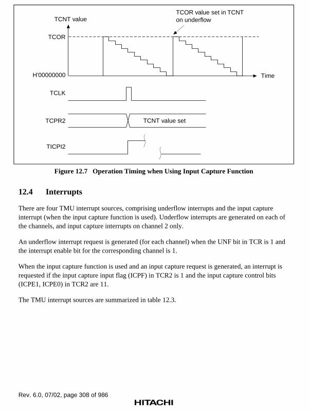
Rev. 6.0, 07/02, page 308 of 986
TCOR
H'00000000
TCLK
TCPR2
TICPI2
TCNT valueTCOR value set in TCNT on underflow
TCNT value set
Time
Figure 12.7 Operation Timing when Using Input Capture Function
12.4 Interrupts
There are four TMU interrupt sources, comprising underflow interrupts and the input captureinterrupt (when the input capture function is used). Underflow interrupts are generated on each ofthe channels, and input capture interrupts on channel 2 only.
An underflow interrupt request is generated (for each channel) when the UNF bit in TCR is 1 andthe interrupt enable bit for the corresponding channel is 1.
When the input capture function is used and an input capture request is generated, an interrupt isrequested if the input capture input flag (ICPF) in TCR2 is 1 and the input capture control bits(ICPE1, ICPE0) in TCR2 are 11.
The TMU interrupt sources are summarized in table 12.3.

Rev. 6.0, 07/02, page 309 of 986
Table 12.3 TMU Interrupt Sources
Channel Interrupt Source Description Priority
0 TUNI0 Underflow interrupt 0 High
1 TUNI1 Underflow interrupt 1
2 TUNI2 Underflow interrupt 2
TICPI2 Input capture interrupt 2
3* TUNI3 Underflow interrupt 3
4* TUNI4 Underflow interrupt 4 Low
Note: * SH7750R only
12.5 Usage Notes
12.5.1 Register Writes
When performing a register write, timer count operation must be stopped by clearing the start bit(STR0–STR4) for the relevant channel in the timer start register (TSTR, TSTR2).
Note that the timer start register (TSTR, TSTR2) can be written to, and the underflow flag (UNF)and input capture flag (ICPF) of the timer control registers (TRCR0 to TCR4) can be clearedwhile the count is in progress. When the flags (UNF, ICPF) are cleared while the count is inprogress, make sure not to change the values of bits other than those being cleared.
12.5.2 TCNT Register Reads
When performing a TCNT register read, processing for synchronization with the timer countoperation is performed. If a timer count operation and register read processing are performedsimultaneously, the TCNT counter value prior to the count-down operation is read by means of thesynchronization processing.
12.5.3 Resetting the RTC Frequency Divider
When the on-chip RTC output clock is selected as the count clock, the RTC frequency dividershould be reset.
12.5.4 External Clock Frequency
Ensure that the external clock frequency for any channel does not exceed Pφ/4.

Rev. 6.0, 07/02, page 310 of 986

Rev. 6.0, 07/02, page 311 of 986
Section 13 Bus State Controller (BSC)
13.1 Overview
The functions of the bus state controller (BSC) include division of the external memory space, andoutput of control signals in accordance with various types of memory and bus interfacespecifications. The BSC functions allow DRAM, synchronous DRAM, SRAM, ROM, etc., to beconnected to the SH7750 Series, and also support the PCMCIA interface protocol, enablingsystem design to be simplified and data transfers to be carried out at high speed by a compactsystem.
13.1.1 Features
The BSC has the following features:
• External memory space is managed as 7 independent areas
Maximum 64 Mbytes for each of areas 0 to 6
Bus width of each area can be set in a register (except area 0, which uses an external pinsetting)
Wait state insertion by RDY pin
Wait state insertion can be controlled by program
Specification of types of memory connectable to each area
Output the control signals of memory to each area
Automatic wait cycle insertion to prevent data bus collisions in case of consecutivememory accesses to different areas, or a read access followed by a write access to the samearea
Write strobe setup time and hold time periods can be inserted in a write cycle to enableconnection to low-speed memory
• SRAM interface
Wait state insertion can be controlled by program
Wait state insertion by RDY pin
Connectable areas: 0 to 6
Settable bus widths: 64, 32, 16, 8
• DRAM interface
Row address/column address multiplexing according to DRAM capacity
Burst operation (fast page mode, EDO mode)
CAS-before-RAS refresh and self-refresh
8-CAS byte control for power-down operation
DRAM control signal timing can be controlled by register settings

Rev. 6.0, 07/02, page 312 of 986
Consecutive accesses to the same row address
Connectable areas: 2, 3
Settable bus widths: 64, 32, 16
• Synchronous DRAM interface
Row address/column address multiplexing according to synchronous DRAM capacity
Burst operation
Auto-refresh and self-refresh
Synchronous DRAM control signal timing can be controlled by register settings
Consecutive accesses to the same row address
Connectable areas: 2, 3
Settable bus widths: 64, 32
• Burst ROM interface
Wait state insertion can be controlled by program
Burst operation, executing the number of transfers set in a register
Connectable areas: 0, 5, 6
Settable bus widths: 64*, 32, 16, 8
• MPX interface
Address/data multiplexing
Connectable areas: 0 to 6
Settable bus widths: 64, 32
• Byte control SRAM interface
SRAM interface with byte control
Connectable areas: 1, 4
Settable bus widths: 64, 32, 16
• PCMCIA interface
Wait state insertion can be controlled by program
Bus sizing function for I/O bus width
• Fine refreshing control
Supports refresh operation immediately after self-refresh operation in low-power DRAMby means of refresh counter overflow interrupt function
• Refresh counter can be used as interval timer
Interrupt request generated by compare-match
Interrupt request generated by refresh counter overflow
Note: * SH7750R only

Rev. 6.0, 07/02, page 313 of 986
13.1.2 Block Diagram
Figure 13.1 shows a block diagram of the BSC.
––
RD/–
, CKE
,
Inte
rnal
bus
Businterface
WCR1
WCR2
WCR3
BCR1
BCR2
BCR3*
BCR4*
PCR
RFCR
RTCNT
RTCOR
RTCSR
ComparatorRefreshcontrol unit
Memorycontrol unit
Areacontrol unit
Waitcontrol unit
Interruptcontroller
BSC
Per
iphe
ral b
us
WCR: Wait control registerBCR: Bus control registerMCR: Memory control registerPCR: PCMCIA control register
Note: * SH7750R only
MCR
Mod
ule
bus
RFCR: Refresh count registerRTCNT: Refresh timer count registerRTCOR: Refresh time constant registerRTCSR: Refresh timer control/status register
Figure 13.1 Block Diagram of BSC

Rev. 6.0, 07/02, page 314 of 986
13.1.3 Pin Configuration
Table 13.1 shows the BSC pin configuration.
Table 13.1 BSC Pins
Name Signals I/O Description
Address bus A25–A0 O Address output
Data bus D63–D52,D31–D0
I/O Data input/output
When port functions are used and DDT mode isselected, input the DTR format. Otherwise, whenport functions are used, D60-D52 cannot be usedand should be left open.
Data bus/port D51–D32/PORT19–PORT0
I/O When port functions are not used: data input/output
When port functions are used: input/output port(input or output set for each bit by register)
Bus cycle start BS O Signal that indicates the start of a bus cycle
When setting synchronous DRAM interface:asserted once for a burst transfer
For other burst transfers: asserted each data cycle
Chip select 6–0 CS6–CS0 O Chip select signals that indicate the area beingaccessed
CS5 and CS6 are also used as PCMCIA CE1A andCE1B
Read/write RD/WR O Data bus input/output direction designation signal
Also used as the DRAM/synchronousDRAM/PCMCIA interface write designation signal
Row addressstrobe
RAS O RAS signal when setting DRAM/synchronous DRAMinterface
Read/columnaddress strobe/cycle frame
RD/CASS/FRAME
O Strobe signal that indicates a read cycle
When setting synchronous DRAM interface: CASsignal
When setting MPX interface: FRAME signal
Data enable 0 WE0/CAS0/DQM0
O When setting synchronous DRAM interface:selection signal for D7–D0
When setting DRAM interface: CAS signal forD7–D0
When setting MPX interface: high-level output
In other cases: write strobe signal for D7–D0

Rev. 6.0, 07/02, page 315 of 986
Table 13.1 BSC Pins (cont)
Name Signals I/O Description
Data enable 1 WE1/CAS1/DQM1
O When setting synchronous DRAM interface:selection signal for D15–D8
When setting DRAM interface: CAS signal forD15–D8
When setting PCMCIA interface: write strobe signal
When setting MPX interface: high-level output
In other cases: write strobe signal for D15–D8
Data enable 2 WE2/CAS2/DQM2/ICIORD
O When setting synchronous DRAM interface:selection signal for D23–D16
When setting DRAM interface: CAS signal forD23–D16
When setting PCMCIA interface: ICIORD signal
When setting MPX interface: high-level output
In other cases: write strobe signal for D23–D16
Data enable 3 WE3/CAS3/DQM3/ICIOWR
O When setting synchronous DRAM interface:selection signal for D31–D24
When setting DRAM interface: CAS signal forD31–D24
When setting PCMCIA interface: ICIOWR signal
When setting MPX interface: high-level output
In other cases: write strobe signal for D31–D24
Data enable 4 WE4/CAS4/DQM4
O When setting synchronous DRAM interface:selection signal for D39–D32
When setting DRAM interface: CAS signal forD39–D32
When setting MPX interface: high-level output
In other cases: write strobe signal for D39–D32
Data enable 5 WE5/CAS5/DQM5
O When setting synchronous DRAM interface:selection signal for D47–D40
When setting DRAM interface: CAS signal forD47–D40
When setting MPX interface: high-level output
In other cases: write strobe signal for D47–D40

Rev. 6.0, 07/02, page 316 of 986
Table 13.1 BSC Pins (cont)
Name Signals I/O Description
Data enable 6 WE6/CAS6/DQM6
O When setting synchronous DRAM interface:selection signal for D55–D48
When setting DRAM interface: CAS signal forD55–D48
When setting MPX interface: high-level output
In other cases: write strobe signal for D55–D48
Data enable 7 WE7/CAS7/DQM7/REG
O When setting synchronous DRAM interface:selection signal for D63–D56
When setting DRAM interface: CAS signal forD63–D56
When setting PCMCIA interface: REG signal
When setting MPX interface: high-level output
In other cases: write strobe signal for D63–D56
Ready RDY I Wait state request signal
Area 0 MPXinterfacespecification/16-bit I/O
MD6/IOIS16 I In power-on reset: Designates area 0 bus as MPXinterface (1: SRAM, 0: MPX)
When setting PCMCIA interface: 16-bit I/Odesignation signal. Valid only in little-endian mode.
Clock enable CKE O Synchronous DRAM clock enable control signal
Bus releaserequest
BREQ/BSACK
I Bus release request signal/bus acknowledge signal
Bus usepermission
BACK/BSREQ
O Bus use permission signal/bus request
Area 0 buswidth/PCMCIAcard select
MD3/CE2A*1
MD4/CE2B*2
I/O In power-on reset*4: external space area 0 bus widthspecification signal
When setting PCMCIA interface: CE2A, CE2B
Endian switchover/row address strobe
MD5/RAS2*3 I/O Endian specification in a power-on reset.*4
RAS2 when DRAM is connected to area 2
Master/slaveswitchover
MD7/TXD I/O Indicates master/slave status in a power-on reset.*4
Serial interface TXD
DMAC0acknowledgesignal
DACK0 O DMAC channel 0 data acknowledge
DMAC1acknowledgesignal
DACK1 O DMAC channel 1 data acknowledge

Rev. 6.0, 07/02, page 317 of 986
Table 13.1 BSC Pins (cont)
Name Signals I/O Description
Read/columnaddress strobe/cycle frame 2
RD2 O Same signal as RD/CASS/FRAME
This signal is used when the RD/CASS/FRAMEsignal load is heavy.
Read/write 2 RD/WR2 O Same signal as RD/WR
This signal is used when the RD/WR signal load isheavy.
Notes: *1 MD3/CE2A input/output switching is performed by BCR1.A56PCM. Output is selectedwhen BCR1.A56PCM = 1.
*2 MD4/CE2B input/output switching is performed by BCR1.A56PCM. Output is selectedwhen BCR1.A56PCM = 1.
*3 MD5/RAS2 input/output switching is performed by BCR1.DRAMTP. Output is selectedwhen BCR1.DRAMTP (2–0) = 101.
*4 In a power-on reset by means of the RESET pin.

Rev. 6.0, 07/02, page 318 of 986
13.1.4 Register Configuration
The BSC has the 11 registers shown in table 13.2. In addition, the synchronous DRAM moderegister incorporated in synchronous DRAM can also be accessed as an SH7750 Series register.The functions of these registers include control of interfaces to various types of memory, waitstates, and refreshing.
Table 13.2 BSC Registers
NameAbbrevia-tion
R/W InitialValue
P4Address
Area 7Address
AccessSize
Bus control register 1 BCR1 R/W H'0000 0000 H'FF80 0000 H'1F80 0000 32
Bus control register 2 BCR2 R/W H'3FFC H'FF80 0004 H'1F80 0004 16
Bus control register 3*2 BCR3 R/W H'0000 H'FF80 0050 H'1F80 0050 16
Bus control register 4*2 BCR4 R/W H'0000 0000 H'FE0A 00F0 H'1E0A 00F0 32
Wait state controlregister 1
WCR1 R/W H'7777 7777 H'FF80 0008 H'1F80 0008 32
Wait state controlregister 2
WCR2 R/W H'FFFE EFFF H'FF80 000C H'1F80 000C 32
Wait state controlregister 3
WCR3 R/W H'0777 7777 H'FF80 0010 H'1F80 0010 32
Memory control register MCR R/W H'0000 0000 H'FF80 0014 H'1F80 0014 32
PCMCIA control register PCR R/W H'0000 H'FF80 0018 H'1F80 0018 16
Refresh timercontrol/status register
RTCSR R/W H'0000 H'FF80 001C H'1F80 001C 16
Refresh timer counter RTCNT R/W H'0000 H'FF80 0020 H'1F80 0020 16
Refresh time constantcounter
RTCOR R/W H'0000 H'FF80 0024 H'1F80 0024 16
Refresh count register RFCR R/W H'0000 H'FF80 0028 H'1F80 0028 16
Forarea 2
SDMR2 W — H'FF90 xxxx*1 H'1F90 xxxx 8SynchronousDRAM moderegisters For
area 3SDMR3 H'FF94 xxxx*1 H'1F94 xxxx
Notes: *1 For details, see section 13.2.10, Synchronous DRAM Mode Registers (SDMR).*2 Settable only for SH7750R.

Rev. 6.0, 07/02, page 319 of 986
13.1.5 Overview of Areas
Space Divisions: The architecture of the SH7750 Series provides a 32-bit virtual address space.The virtual address is divided into five areas according to the upper address value. Externalmemory space comprises a 29-bit address space, divided into eight areas.
The virtual address can be allocated to any external address by means of the memory managementunit (MMU). Details are given in section 3, Memory Management Unit (MMU). This sectiondescribes the areas into which the external address is divided.
With the SH7750 Series, various kinds of memory or PC cards can be connected to the sevenareas of external address as shown in table 13.3, and chip select signals (CS0–CS6, CE2A, CE2B)are output for each of these areas. CS0 is asserted when accessing area 0, and CS6 when accessingarea 6. When DRAM or synchronous DRAM is connected to area 2 or 3, signals such as RAS,CAS, RD/WR, and DQM are also asserted. When the PCMCIA interface is selected for area 5 or6, CE2A, CE2B is asserted in addition to CS5, CS6 for the byte to be accessed.
H'0000 0000
H'8000 0000
H'A000 0000
H'C000 0000
H'E000 0000
H'FFFF FFFFH'E400 0000
H'0000 0000
H'0400 0000
H'0800 0000
H'0C00 0000
H'1000 0000
H'1400 0000
H'1800 0000
H'1FFF FFFFH'1C00 0000
Area 0 ( )
Area 1 ( )
Area 2 ( )
Area 3 ( )
Area 4 ( )
Area 5 ( )
Area 6 ( )
Area 7 (reserved area)
P0 andU0 areas
P1 area
P2 area
P3 area
Physical address space
(MMU off)
Virtual address space
(MMU on)
External memoryspace
Store queue areaP4 area
P0 andU0 areas
256
P1 area
P2 area
P3 area
Store queue areaP4 area
Notes: 1. When the MMU is off (MMUCR.AT = 0), the top 3 bits of the 32-bit address are ignored, and memory is mapped onto a fixed 29-bit external address.
2. When the MMU is on (MMUCR.AT = 1), the P0, U0, P3, and store queue areas can be mapped onto any external address using the TLB.
For details, see section 3, Memory Management Unit (MMU).
Figure 13.2 Correspondence between Virtual Address Space and External Memory Space
Rev. 6.0, 07/02, page 320 of 986
Table 13.3 External Memory Space Map
AreaExternalAddresses Size
ConnectableMemory
Settable BusWidths Access Size
SRAM 8, 16, 32, 64*1
Burst ROM 8, 16, 32*1, 64*7
0 H'00000000–H'03FFFFFF
64 Mbytes
MPX 32, 64*1
8, 16, 32,64*6 bits,32 bytes
SRAM 8, 16, 32, 64*2
MPX 32, 64*2
1 H'04000000–H'07FFFFFF
64 Mbytes
Byte control SRAM 16, 32, 64*2
8, 16, 32,64*6 bits,32 bytes
SRAM 8, 16, 32, 64*2
Synchronous DRAM 32, 64*2 *3
DRAM 16, 32*2 *3
2 H'08000000–H'0BFFFFFF
64 Mbytes
MPX 32, 64*2
8, 16, 32,64*6 bits,32 bytes
SRAM 8, 16, 32, 64*2
Synchronous DRAM 32, 64*2 *3
DRAM 16, 32, 64*2 *3
3 H'0C000000–H'0FFFFFFF
64 Mbytes
MPX 32, 64*2
8, 16, 32,64*6 bits,32 bytes
SRAM 8, 16, 32, 64*2
MPX 32, 64*2
4 H'10000000–H'13FFFFFF
64 Mbytes
Byte control RAM 16, 32, 64*2
8, 16, 32,64*6 bits,32 bytes
SRAM 8, 16, 32, 64*2
MPX 32, 64*2
Burst ROM 8, 16, 32*2, 64*7
5 H'14000000–H'17FFFFFF
64 Mbytes
PCMCIA 8, 16*2 *4
8, 16, 32,64*6 bits,32 bytes
SRAM 8, 16, 32, 64*2
MPX 32, 64*2
Burst ROM 8,16, 32*2, 64*7
6 H'18000000–H'1BFFFFFF
64 Mbytes
PCMCIA 8,16*2 *4
8, 16, 32,64*6 bits,32 bytes
7*5 H'1C000000–H'1FFFFFFF
64 Mbytes — —
Notes: *1 Memory bus width specified by external pins*2 Memory bus width specified by register*3 With synchronous DRAM interface, bus width is 32 or 64 bits only.
With DRAM interface, bus width is 16 or 32 bits only for area 2, and 16, 32, or 64 bitsonly for area 3. Bus width of area 2 is as same as that of area 3 which is specified byMCR.
*4 With PCMCIA interface, bus width is 8 or 16 bits only.
*5 Do not access a reserved area, as operation cannot be guaranteed in this case.*6 64-bit access applies only to transfer by the DMAC. (CHCRn. TS = 000)
In a transfer to an external memory by FMOV (FPSCR.SZ = 1), two transfer operations,each with an access size of 32 bits, are conducted.
*7 Settable only for SH7750R.

Rev. 6.0, 07/02, page 321 of 986
Area 0: H'00000000
Area 1: H'04000000
Area 2: H'08000000
Area 3: H'0C000000
Area 4: H'10000000
Area 5: H'14000000
Area 6: H'18000000
SRAM/burst ROM/MPX
SRAM/MPX/byte control SRAM
SRAM/synchronous DRAM/DRAM/MPX
SRAM/synchronous DRAM/DRAM/MPX
SRAM/MPX/byte control SRAM
SRAM/burst ROM/PCMCIA/MPX
SRAM/burst ROM/PCMCIA/MPX
The PCMCIA interface is for memory and I/O card use
Figure 13.3 External Memory Space Allocation
Memory Bus Width: In the SH7750 Series, the memory bus width can be set independently foreach space. For area 0, a bus size of 8, 16, 32, or 64 bits can be selected in a power-on reset by theRESET pin, using external pins. The relationship between the external pins (MD4 and MD3) andthe bus width in a power-on reset is shown below.
MD4 MD3 Bus Width
0 0 64 bits
1 8 bits
1 0 16 bits
1 32 bits
When SRAM interface or ROM is used in areas 1 to 6, a bus width of 8, 16, 32, or 64 bits can beselected with bus control register 2 (BCR2). When burst ROM is used, a bus width of 8, 16, 32, or64* bits can be selected. When byte control SRAM interface is used, a bus width of 16, 32, or 64bits can be selected. When the MPX interface is used, a bus width of 32 or 64 bits can be selected.When the DRAM interface is used, a bus width of 16, 32, or 64 bits can be selected with thememory control register (MCR). When the DRAM interface is used for area 2 or 3, a bus width of16 or 32 bits should be set. For the synchronous DRAM interface, set a bus width of 32 or 64 bitsin the MCR register.

Rev. 6.0, 07/02, page 322 of 986
When using the PCMCIA interface, set a bus width of 8 or 16 bits.
For details, see section 13.3.7, PCMCIA Interface.
When using port functions, set a bus width of 8, 16, or 32 bits for all areas.
For details, see section 13.2.2, Bus Control Register 2 (BCR2), and section 13.2.7, MemoryControl Register (MCR).
The area 7 address range, H'1C000000 to H'1FFFFFFFF, is a reserved space and must not be used.
Note: * SH7750R only
13.1.6 PCMCIA Support
The SH7750 Series supports PCMCIA compliant interface specifications for external memoryspace areas 5 and 6.
The interfaces supported are the IC memory card interface and I/O card interface stipulated inJEIDA specifications version 4.2 (PCMCIA2.1).
External memory space areas 5 and 6 support both the IC memory card interface and the I/O cardinterface.
The PCMCIA interface is supported only in little-endian mode.
Table 13.4 PCMCIA Interface Features
Item Features
Access Random access
Data bus 8/16 bits
Memory type Mask ROM, OTPROM, EPROM, EEPROM, flash memory, SRAM
Common memory capacity Max. 64 Mbytes
Attribute memory capacity Max. 64 Mbytes
Others Dynamic bus sizing for I/O bus width, access to PCMCIA interfacefrom address translation areas

Rev. 6.0, 07/02, page 323 of 986
Table 13.5 PCMCIA Support Interfaces
IC Memory Card Interface I/O Card Interface
PinSignalName I/O Function
SignalName I/O Function
CorrespondingSH7750 SeriesPin
1 GND Ground GND Ground —
2 D3 I/O Data D3 I/O Data D3
3 D4 I/O Data D4 I/O Data D4
4 D5 I/O Data D5 I/O Data D5
5 D6 I/O Data D6 I/O Data D6
6 D7 I/O Data D7 I/O Data D7
7 CE1 I Card enable CE1 I Card enable CS5 or CS6
8 A10 I Address A10 I Address A10
9 OE I Output enable OE I Output enable RD
10 A11 I Address A11 I Address A11
11 A9 I Address A9 I Address A9
12 A8 I Address A8 I Address A8
13 A13 I Address A13 I Address A13
14 A14 I Address A14 I Address A14
15 WE/PGM I Write enable WE/PGM I Write enable WE1
16 RDY/BSY O Ready/busy IREQ O Interrupt request Sensed on port
17 VCC Operating powersupply
VCC Operating powersupply
—
18 VPP1 Programmingpower supply
VPP1 Programming/peripheral powersupply
—
19 A16 I Address A16 I Address A16
20 A15 I Address A15 I Address A15
21 A12 I Address A12 I Address A12
22 A7 I Address A7 I Address A7
23 A6 I Address A6 I Address A6
24 A5 I Address A5 I Address A5
25 A4 I Address A4 I Address A4
26 A3 I Address A3 I Address A3
27 A2 I Address A2 I Address A2
28 A1 I Address A1 I Address A1

Rev. 6.0, 07/02, page 324 of 986
Table 13.5 PCMCIA Support Interfaces (cont)
IC Memory Card Interface I/O Card Interface
PinSignalName I/O Function
SignalName I/O Function
CorrespondingSH7750 SeriesPin
29 A0 I Address A0 I Address A0
30 D0 I/O Data D0 I/O Data D0
31 D1 I/O Data D1 I/O Data D1
32 D2 I/O Data D2 I/O Data D2
33 WP* O Write protect IOIS16 O 16-bit I/O port IOIS16
34 GND Ground GND Ground —
35 GND Ground GND Ground —
36 CD1 O Card detection CD1 O Card detection Sensed on port
37 D11 I/O Data D11 I/O Data D11
38 D12 I/O Data D12 I/O Data D12
39 D13 I/O Data D13 I/O Data D13
40 D14 I/O Data D14 I/O Data D14
41 D15 I/O Data D15 I/O Data D15
42 CE2 I Card enable CE2 I Card enable CE2A or CE2B
43 RFSH I Refresh request RFSH I Refresh request Output fromport
44 RFU Reserved IORD I I/O read ICIORD
45 RFU Reserved IOWR I I/O write ICIOWR
46 A17 I Address A17 I Address A17
47 A18 I Address A18 I Address A18
48 A19 I Address A19 I Address A19
49 A20 I Address A20 I Address A20
50 A21 I Address A21 I Address A21
51 VCC Power supply VCC Power supply —
52 VPP2 Programmingpower supply
VPP2 Programming/peripheral powersupply
—
53 A22 I Address A22 I Address A22
54 A23 I Address A23 I Address A23
55 A24 I Address A24 I Address A24
56 A25 I Address A25 I Address A25

Rev. 6.0, 07/02, page 325 of 986
Table 13.5 PCMCIA Support Interfaces (cont)
IC Memory Card Interface I/O Card Interface
PinSignalName I/O Function
SignalName I/O Function
CorrespondingSH7750 SeriesPin
57 RFU Reserved RFU Reserved —
58 RESET I Reset RESET I Reset Output fromport
59 WAIT O Wait request WAIT O Wait request RDY
60 RFU Reserved INPACK O Input acknowledge —
61 REG I Attribute memoryspace select
REG I Attribute memoryspace select
WE7
62 BVD2 O Battery voltagedetection
SPKR O Digital speechsignal
Sensed on port
63 BVD1 O Battery voltagedetection
STSCHG O Card statuschange
Sensed on port
64 D8 I/O Data D8 I/O Data D8
65 D9 I/O Data D9 I/O Data D9
66 D10 I/O Data D10 I/O Data D10
67 CD2 O Card detection CD2 O Card detection Sensed on port
68 GND Ground GND Ground —
Note: * WP is not supported.

Rev. 6.0, 07/02, page 326 of 986
13.2 Register Descriptions
13.2.1 Bus Control Register 1 (BCR1)
Bus control register 1 (BCR1) is a 32-bit readable/writable register that specifies the function, buscycle status, etc., of each area.
BCR1 is initialized to H'00000000 by a power-on reset, but is not initialized by a manual reset orin standby mode. External memory space other than area 0 should not be accessed until registerinitialization is completed.
Bit: 31 30 29 28 27 26 25 24
ENDIAN MASTER A0MPX — — DPUP*2 IPUP OPUP
Initial value: 0/1*1 0/1*1 0/1*1 0 0 0 0 0
R/W: R R R R R R R/W R/W
Bit: 23 22 21 20 19 18 17 16
— — A1MBC A4MBC BREQEN PSHR MEMMPX DMABST*2
Initial value: 0 0 0 0 0 0 0 0
R/W: R R R/W R/W R/W R/W R/W R
Bit: 15 14 13 12 11 10 9 8
HIZMEM HIZCNT A0BST2 A0BST1 A0BST0 A5BST2 A5BST1 A5BST0
Initial value: 0 0 0 0 0 0 0 0
R/W: R/W R/W R/W R/W R/W R/W R/W R/W
Bit: 7 6 5 4 3 2 1 0
A6BST2 A6BST1 A6BST0 DRAMTP2 DRAMTP1 DRAMTP0 — A56PCM
Initial value: 0 0 0 0 0 0 0 0
R/W: R/W R/W R/W R/W R/W R/W R R/W
Notes: *1 These bits sample external pin values in a power-on reset by means of the RESET pin.*2 SH7750R only.

Rev. 6.0, 07/02, page 327 of 986
Bit 31—Endian Flag (ENDIAN): Samples the value of the endian specification external pin(MD5) in a power-on reset by the RESET pin. The endian mode of all spaces is determined by thisbit. ENDIAN is a read-only bit.
Bit 31: ENDIAN Description
0 In a power-on reset, the endian setting external pin (MD5) is low,designating big-endian mode
1 In a power-on reset, the endian setting external pin (MD5) is high,designating little-endian mode
Bit 30—Master/Slave Flag (MASTER): Samples the value of the master/slave specificationexternal pin (MD7) in a power-on reset by the RESET pin. The master/slave status of all spaces isdetermined by this bit. MASTER is a read-only bit.
Bit 30: MASTER Description
0 In a power-on reset, the master/slave setting external pin (MD7) is high,designating master mode
1 In a power-on reset, the master/slave setting external pin (MD7) is low,designating slave mode
Bit 29—Area 0 Memory Type (A0MPX): Samples the value of the area 0 memory typespecification external pin (MD6) in a power-on reset by the RESET pin. The memory type of area0 is determined by this bit. A0MPX is a read-only bit.
Bit 29: A0MPX Description
0 In a power-on reset, the external pin specifying the area 0 memory type(MD6) is high, designating the area 0 as SRAM interface
1 In a power-on reset, the external pin specifying the area 0 memory type(MD6) is low, designating the area 0 as MPX interface
Bits 28, 27, 26*, 23, 22, 16*, and 1—Reserved: These bits are always read as 0, and should onlybe written with 0.
Note: * SH7750, SH7750S only.

Rev. 6.0, 07/02, page 328 of 986
Bit 26—Data pin Pullup Resistor Control (DPUP) (SH7750R only): Controls the pullupresistance of the data pins (D63 to D0). It is initialized at a power-on reset. The pins are not pulledup when access is performed or when the bus is released, even if the ON setting is selected.
Bit 26: DPUP Description
0 Sets pullup resistance of data pins (D63 to D0) ON (Initial value)
1 Sets pullup resistance of data pins (D63 to D0) OFF
Bit 25—Control Input Pin Pull-Up Resistor Control (IPUP): Specifies the pull-up resistorstatus for control input pins (NMI, IRL0–IRL3, BREQ, MD6/IOIS16, RDY). IPUP is initializedby a power-on reset.
Bit 25: IPUP Description
0 Pull-up resistor is on for control input pins (NMI, IRL0–IRL3, BREQ,MD6/IOIS16, RDY) (Initial value)
1 Pull-up resistor is off for control input pins (NMI, IRL0–IRL3, BREQ,MD6/IOIS16, RDY)
Bit 24—Control Output Pin Pull-Up Resistor Control (OPUP): Specifies the pull-up resistorstatus for control output pins (A[25:0], BS, CSn, RD, WEn, RD/WR, RAS, RAS2, CE2A, CE2B,RD2, RD/WR2) when high-impedance. OPUP is initialized by a power-on reset.
Bit 24: OPUP Description
0 Pull-up resistor is on for control output pins (A[25:0], BS, CSn, RD, WEn,RD/WR, RAS, RAS2, CE2A, CE2B, RD2, RD/WR2) (Initial value)
1 Pull-up resistor is off for control output pins (A[25:0], BS, CSn, RD, WEn,RD/WR, RAS, RAS2, CE2A, CE2B, RD2, RD/WR2)
Bit 21—Area 1 SRAM Byte Control Mode (A1MBC): MPX interface has priority when anMPX interface is set. This bit is initialized by a power-on reset.
Bit 21: A1MBC Description
0 Area 1 SRAM is set to normal mode (Initial value)
1 Area 1 SRAM is set to byte control mode
Rev. 6.0, 07/02, page 329 of 986
Bit 20—Area 4 SRAM Byte Control Mode (A4MBC): MPX interface has priority when anMPX interface is set. This bit is initialized by a power-on reset.
Bit 20: A4MBC Description
0 Area 4 SRAM is set to normal mode (Initial value)
1 Area 4 SRAM is set to byte control mode
Bit 19—BREQ Enable (BREQEN): Indicates whether external requests can be accepted.BREQEN is initialized to the external request acceptance disabled state by a power-on reset. It isignored in the case of a slave mode startup.
Bit 19: BREQEN Description
0 External requests are not accepted (Initial value)
1 External requests are accepted
Bit 18—Partial-Sharing Bit (PSHR): Sets partial-sharing mode. PSHR is valid only in the caseof a master mode startup.
Bit 18: PSHR Description
0 Master mode (Initial value)
1 Partial-sharing mode
Bit 17—Area 1 to 6 MPX Interface Specification (MEMMPX): Sets the MPX interface whenareas 1 to 6 are set as SRAM interface (or burst ROM interface). MEMMPX is initialized by apower-on reset.
Bit 17: MEMMPX Description
0 SRAM interface (or burst ROM interface) is selected when areas 1 to 6 areset as SRAM interface (or burst ROM interface) (Initial value)
1 MPX interface is selected when areas 1 to 6 are set as SRAM interface (orburst ROM interface)
Rev. 6.0, 07/02, page 330 of 986
Bit 16—DMAC Burst Mode Transfer Priority Setting (DMABST) (SH7750R Only):Specifies the priority of burst mode transfers by the DMAC. When OFF, the priority is as follows:bus privilege released, refresh, DMAC, CPU. When ON, the bus privileges are released andrefresh operations are not performed until the end of the DMAC’s burst transfer. This bit isinitialized at a power-on reset.
Bit 16: DMABST Description
0 DMAC burst mode transfer priority specification OFF (Initial value)
1 DMAC burst mode transfer priority specification ON
Bit 15—High Impedance Control (HIZMEM): Specifies the state of address and other signals(A[25:0], BS, CSn, RD/WR, CE2A, CE2B) in software standby mode.
Bit 15: HIZMEM Description
0 The A[25:0], BS, CSn, RD/WR, CE2A, and CE2B signals go to high-impedance (High-Z) in standby mode and when the bus is released
(Initial value)
1 The A[25:0], BS, CSn, RD/WR, CE2A, and CE2B signals are driven instandby mode. When the bus is released, they go to high-impedance.
Bit 14—High Impedance Control (HIZCNT): Specifies the state of the RAS and CAS signals insoftware standby mode and when the bus is released.
Bit 14: HIZCNT Description
0 The RAS, RAS2, WEn/CASn/DQMn, RD/CASS/FRAME, and RD2 signalsgo to high-impedance (High-Z) in standby mode and when the bus isreleased (Initial value)
1 The RAS, RAS2, WEn/CASn/DQMn, RD/CASS/FRAME, and RD2 signalsare driven in standby mode and when the bus is released
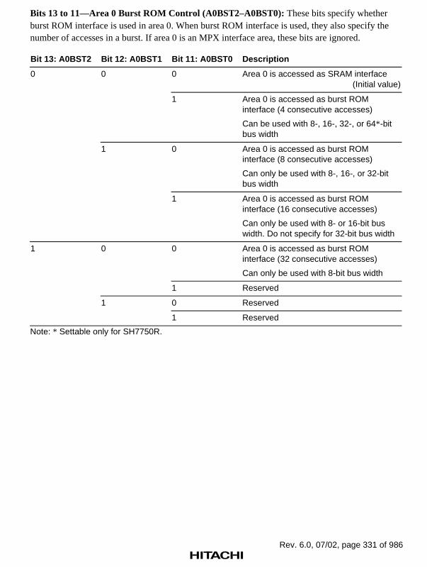
Rev. 6.0, 07/02, page 331 of 986
Bits 13 to 11—Area 0 Burst ROM Control (A0BST2–A0BST0): These bits specify whetherburst ROM interface is used in area 0. When burst ROM interface is used, they also specify thenumber of accesses in a burst. If area 0 is an MPX interface area, these bits are ignored.
Bit 13: A0BST2 Bit 12: A0BST1 Bit 11: A0BST0 Description
0 0 0 Area 0 is accessed as SRAM interface (Initial value)
1 Area 0 is accessed as burst ROMinterface (4 consecutive accesses)
Can be used with 8-, 16-, 32-, or 64*-bitbus width
1 0 Area 0 is accessed as burst ROMinterface (8 consecutive accesses)
Can only be used with 8-, 16-, or 32-bitbus width
1 Area 0 is accessed as burst ROMinterface (16 consecutive accesses)
Can only be used with 8- or 16-bit buswidth. Do not specify for 32-bit bus width
1 0 0 Area 0 is accessed as burst ROMinterface (32 consecutive accesses)
Can only be used with 8-bit bus width
1 Reserved
1 0 Reserved
1 Reserved
Note: * Settable only for SH7750R.

Rev. 6.0, 07/02, page 332 of 986
Bits 10 to 8—Area 5 Burst Enable (A5BST2–A5BST0): These bits specify whether burst ROMinterface is used in area 5. When burst ROM interface is used, they also specify the number ofaccesses in a burst. If area 5 is an MPX interface area, these bits are ignored.
Bit 10: A5BST2 Bit 9: A5BST1 Bit 8: A5BST0 Description
0 0 0 Area 5 is accessed as SRAM interface(Initial value)
1 Area 5 is accessed as burst ROMinterface (4 consecutive accesses)
Can be used with 8-, 16-, 32-, or 64*-bitbus width
1 0 Area 5 is accessed as burst ROMinterface (8 consecutive accesses)
Can only be used with 8-, 16-, or 32-bitbus width
1 Area 5 is accessed as burst ROMinterface (16 consecutive accesses)
Can only be used with 8- or 16-bit buswidth. Do not specify for 32-bit bus width
1 0 0 Area 5 is accessed as burst ROMinterface (32 consecutive accesses)
Can only be used with 8-bit bus width
1 Reserved
1 0 Reserved
1 Reserved
Note: Clear to 0 when PCMCIA interface is set.
* Settable only for SH7750R.

Rev. 6.0, 07/02, page 333 of 986
Bits 7 to 5—Area 6 Burst Enable (A6BST2–A6BST0): These bits specify whether burst ROMinterface is used in area 6. When burst ROM interface is used, they also specify the number ofaccesses in a burst. If area 6 is an MPX interface area, these bits are ignored.
Bit 7: A6BST2 Bit 6: A6BST1 Bit 5: A6BST0 Description
0 0 0 Area 6 is accessed as SRAM interface(Initial value)
1 Area 6 is accessed as burst ROMinterface (4 consecutive accesses)
Can be used with 8-, 16-, 32-, or 64*-bitbus width
1 0 Area 6 is accessed as burst ROMinterface (8 consecutive accesses)
Can only be used with 8-, 16-, or 32-bitbus width
1 Area 6 is accessed as burst ROMinterface (16 consecutive accesses)
Can only be used with 8- or 16-bit buswidth. Do not specify for 32-bit bus width
1 0 0 Area 6 is accessed as burst ROMinterface (32 consecutive accesses)
Can only be used with 8-bit bus width
1 Reserved
1 0 Reserved
1 Reserved
Note: Clear to 0 when PCMCIA interface is set.
* Settable only for SH7750R.

Rev. 6.0, 07/02, page 334 of 986
Bits 4 to 2—Area 2 and 3 Memory Type (DRAMTP2–DRAMTP0): These bits specify the typeof memory connected to areas 2 and 3. ROM, SRAM, flash ROM, etc., can be connected asSRAM interface. DRAM and synchronous DRAM can also be connected.
Bit 4: DRAMTP2 Bit 3: DRAMTP1 Bit 2: DRAMTP0 Description
0 0 0 Areas 2 and 3 are SRAM interface orMPX interface*1
(Initial value)
1 Reserved (Cannot be set)
1 0 Area 2 is SRAM interface or MPXinterface*1, area 3 is synchronous DRAMinterface
1 Areas 2 and 3 are synchronous DRAMinterface
1 0 0 Area 2 is SRAM interface or MPXinterface*1, area 3 is DRAM interface
1 Areas 2 and 3 are DRAM interface*2
1 0 Reserved (Cannot be set)
1 Reserved (Cannot be set)
Note: *1 Selection of SRAM interface or MPX interface is determined by the setting of theMEMMPX bit
*2 When this mode is selected, 16 or 32 bits should be specified as the bus width for areas2 and 3. In this mode the MD5 pin is designated for output as the RAS2 pin.
Bit 0—Area 5 and 6 Bus Type (A56PCM): Specifies whether areas 5 and 6 are accessed asPCMCIA interface. The setting of these bits has priority over the MEMMPX bit settings.
Bit 0: A56PCM Description
0 Areas 5 and 6 are accessed as SRAM interface (Initial value)
1 Areas 5 and 6 are accessed as PCMCIA interface*
Note: * The MD3 pin is designated for output as the CE2A pin.The MD4 pin is designated for output as the CE2B pin.

Rev. 6.0, 07/02, page 335 of 986
13.2.2 Bus Control Register 2 (BCR2)
Bus control register 2 (BCR2) is a 16-bit readable/writable register that specifies the bus width foreach area, and whether a 16-bit port is used.
BCR2 is initialized to H'3FFC by a power-on reset, but is not initialized by a manual reset or instandby mode. External memory space other than area 0 should not be accessed until registerinitialization is completed.
Bit: 15 14 13 12 11 10 9 8
Bit name: A0SZ1 A0SZ0 A6SZ1 A6SZ0 A5SZ1 A5SZ0 A4SZ1 A4SZ0
Initial value: 0/1* 0/1* 1 1 1 1 1 1
R/W: R R R/W R/W R/W R/W R/W R/W
Bit: 7 6 5 4 3 2 1 0
Bit name: A3SZ1 A3SZ0 A2SZ1 A2SZ0 A1SZ1 A0SZ0 — PORTEN
Initial value: 1 1 1 1 1 1 0 0
R/W: R/W R/W R/W R/W R/W R/W — R/W
Note: * These bits sample the values of the external pins that specify the area 0 bus size.
Bits 15 and 14—Area 0 Bus Width (A0SZ1, A0SZ0): These bits sample the external pins, MD4and MD3 that specify the bus size in a power-on reset by the RESET pin. They are read-only bits.
Bit 15 Bit 14
A0SZ1 A0SZ0 Description
0 0 Bus width is 64 bits
1 Bus width is 8 bits
1 0 Bus width is 16 bits
1 Bus width is 32 bits

Rev. 6.0, 07/02, page 336 of 986
Bits 2n + 1, 2n—Area n (1 to 6) Bus Width Specification (AnSZ1, AnSZ0): These bits specifythe bus width of area n (n = 1 to 6).
(Bit 0): PORTEN Bit 2n + 1: AnSZ1 Bit 2n: AnSZ0 Description
0 0 0 Bus width is 64 bits
1 Bus width is 8 bits
1 0 Bus width is 16 bits
1 Bus width is 32 bits (Initial value)
1 0 0 Reserved (Setting prohibited)
1 Bus width is 8 bits
1 0 Bus width is 16 bits
1 Bus width is 32 bits
Bit 1—Reserved: This bit is always read as 0, and should only be written with 0.
Bit 0—Port Function Enable (PORTEN): Specifies whether pins D51 to D32 are used as a 20-bit port. When this function is used, a bus width of 8, 16, or 32 bits should be set for all areas.
Bit 0: PORTEN Description
0 D51 to D32 are not used as a port (Initial value)
1 D51 to D32 are used as a port

Rev. 6.0, 07/02, page 337 of 986
13.2.3 Bus Control Register 3 (BCR3) (SH7750R Only)
Bus control register 3 (BCR3) is a 16-bit readable/writable register that specifies the selection ofeither the MPX interface or the SRAM interface and specifies the burst length when thesynchronous DRAM interface is used.
BCR3 is initialized to H'0000 by a power-on reset, but is not initialized by a manual reset or instandby mode. No external memory space other than area 0 should be accessed before registerinitialization has been completed.
Bit: 15 14 13 12 11 10 9 8
Bit name: MEMMODE A1MPX A4MPX — — — — —
Initial value: 0 0 0 0 0 0 0 0
R/W: R/W R/W R/W R R R R R
Bit: 7 6 5 4 3 2 1 0
Bit name: — — — — — — — SDBL
Initial value: 0 0 0 0 0 0 0 0
R/W: R R R R R R R R/W
Bit 15 A1MPX/A4MPX Enable (MEMMODE): Determines whether or not the selection ofeither the MPX interface or the SRAM interface is by A1MPX and A4MPX rather than byMEMMPX.
Bit 15: MEMMODE Description
0 MPX or SRAM interface is selected by MEMMPX (Initial value)
1 MPX or SRAM interface is selected by A1MPX and A4MPX
Bits 14 and 13 MPX-Interface Specification for Area 1 and 4 (A1MPX, A4MPX): Thesebits specify the types of memory connected to areas 1 and 4. These settings are validated byMEMMODE.
Bit 14: A1MPX Description
0 SRAM/byte control SRAM interface is selected for area 1 (Initial value)
1 MPX interface is selected for area 1
Bit 13: A4MPX Description
0 SRAM/byte control SRAM interface is selected for area 4 (Initial value)
1 MPX interface is selected for area 4

Rev. 6.0, 07/02, page 338 of 986
Bits 12 to 1—Reserved: These bits are always read as 0, and should only be written with 0.
Bit 0 Burst Length (SDBL): Sets the burst length when the synchronous DRAM interface isused. The burst-length setting is only valid when the bus width is 32 bits.
Bit 0: SDBL Description
0 Burst length is 8 (Initial value)
1 Burst length is 4
13.2.4 Bus Control Register 4 (BCR4) (SH7750R Only)
Bus control register 4 (BCR4) is a 32-bit readable/writable register that enables asynchronousinput to the pin corresponding to each bit.
BCR4 is initialized to H'00000000 by a power-on reset, but is not initialized by a manual reset orin standby mode.
When asynchronous input is set (ASYNCn = 1), the sampling timing is one cycle earlier thanwhen synchronous input is set (ASYNCn = 0)* (see figure 13.4)
The timings shown in this section and section 22, Electrical Characteristics, are all for the casewhere synchronous input is set (ASYNCn = 0).
Note: * With the synchronous input setting, ensure that setup and hold times are observed.
T1 Tw Tw Twe T2
CKIO
(BCR4.ASYNC0 = 0)
(BCR4.ASYNC0 = 1)
Figure 13.4 Example of RDYRDYRDYRDY Sampling Timing at which BCR4 is Set(Two Wait Cycles are Inserted by WCR2)

Rev. 6.0, 07/02, page 339 of 986
Bit: 31 30 29 28 27 26 25 24
Bit name: — — — — — — — —
Initial value: 0 0 0 0 0 0 0 0
R/W: R R R R R R R R
Bit: 23 22 21 20 19 18 17 16
Bit name: — — — — — — — —
Initial value: 0 0 0 0 0 0 0 0
R/W: R R R R R R R R
Bit: 15 14 13 12 11 10 9 8
Bit name: — — — — — — — —
Initial value: 0 0 0 0 0 0 0 0
R/W: R R R R R R R R
Bit: 7 6 5 4 3 2 1 0
Bit name: — — — ASYNC
Initial value: 0 0 0 0 0 0 0 0
R/W: R R R R/W R/W R/W R/W R/W
Bits 31 to 5 Reserved: These bits are always read as 0, and should only be written with 0.
Bits 4 to 0 Asynchronous Input: These bits enable asynchronous input to the correspondingpin.
Bits 4 to 0: ASYNCn Description
0 Input to corresponding pin is synchronous with CKIO (Initial value)
1 Input to corresponding pin can be asynchronous with CKIO
Bit Corresponding Pin
4 IOIS16
3 DREQ1
2 DREQ0
1 BREQ
0 RDY

Rev. 6.0, 07/02, page 340 of 986
13.2.5 Wait Control Register 1 (WCR1)
Wait control register 1 (WCR1) is a 32-bit readable/writable register that specifies the number ofidle state insertion cycles for each area. With some kinds of memory, data bus drive does not gooff immediately after the read signal from off-chip goes off. As a result, there is a possibility of adata bus collision when consecutive memory accesses are performed on memory in differentareas, or when a memory write is performed immediately after a read. In the SH7750 Series, thenumber of idle cycles set in the WCR1 register are inserted automatically if there is a possibility ofthis kind of data bus collision.
WCR1 is initialized to H'77777777 by a power-on reset, but is not initialized by a manual reset orin standby mode.
Bit: 31 30 29 28 27 26 25 24
Bit name: — DMAIW2 DMAIW1 DMAIW0 — A6IW2 A6IW1 A6IW0
Initial value: 0 1 1 1 0 1 1 1
R/W: R R/W R/W R/W R R/W R/W R/W
Bit: 23 22 21 20 19 18 17 16
Bit name: — A5IW2 A5IW1 A5IW0 — A4IW2 A4IW1 A4IW0
Initial value: 0 1 1 1 0 1 1 1
R/W: R R/W R/W R/W R R/W R/W R/W
Bit: 15 14 13 12 11 10 9 8
Bit name: — A3IW2 A3IW1 A3IW0 — A2IW2 A2IW1 A2IW0
Initial value: 0 1 1 1 0 1 1 1
R/W: R R/W R/W R/W R R/W R/W R/W
Bit: 7 6 5 4 3 2 1 0
Bit name: — A1IW2 A1IW1 A1IW0 — A0IW2 A0IW1 A0IW0
Initial value: 0 1 1 1 0 1 1 1
R/W: R R/W R/W R/W R R/W R/W R/W
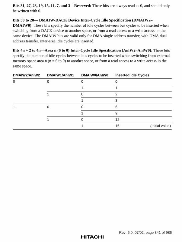
Rev. 6.0, 07/02, page 341 of 986
Bits 31, 27, 23, 19, 15, 11, 7, and 3—Reserved: These bits are always read as 0, and should onlybe written with 0.
Bits 30 to 28— DMAIW-DACK Device Inter-Cycle Idle Specification (DMAIW2–DMAIW0): These bits specify the number of idle cycles between bus cycles to be inserted whenswitching from a DACK device to another space, or from a read access to a write access on thesame device. The DMAIW bits are valid only for DMA single address transfer; with DMA dualaddress transfer, inter-area idle cycles are inserted.
Bits 4n + 2 to 4n—Area n (6 to 0) Inter-Cycle Idle Specification (AnlW2–AnlW0): These bitsspecify the number of idle cycles between bus cycles to be inserted when switching from externalmemory space area n (n = 6 to 0) to another space, or from a read access to a write access in thesame space.
DMAIW2/AnIW2 DMAIW1/AnIW1 DMAIW0/AnIW0 Inserted Idle Cycles
0 0 0 0
1 1
1 0 2
1 3
1 0 0 6
1 9
1 0 12
1 15 (Initial value)

Rev. 6.0, 07/02, page 342 of 986
• Idle Insertion between Accesses
Following Cycle
Same Area Different AreaSameArea
DifferentArea
Read Write Read WritePrecedingCycle CPU DMA CPU DMA CPU DMA CPU DMA
MPXAddressOutput
MPXAddressOutput
Read M M M M M M M (1) M (1)
Write M M M M *2 M
DMA read(memory →device)
M M M M M M — M (1)
DMA write(device →memory)
D D D D*1 D D D D — D (1)
“DMA” in the table indicates DMA single-address transfer. DMA dual transfer is in accordance withthe CPU.M, D: Idle wait always inserted by WCR1
(M(1): One cycle inserted in MPX access even if WCR1 is cleared to 0)
M: Idle cycles according to setting of AnIW2-AnIW0 (area 0 to area 6)D: Idle cycles according to setting of DMAIW2-DMAIW0Notes: When synchronous DRAM is used in RAS down mode, set bits DMAIW2-DMAIW0 to 000
and bits A3IW2-A3IW0 to 000.*1 Inserted when device is switched*2 On the MPX interface, a WCR1 idle wait may be inserted before an access (either read
or write) to the same area after a write access. The specific conditions for idle waitinsertion in accesses to the same area are shown below.(a) Synchronous DRAM set to RAS down mode
(b) Synchronous DRAM accessed by on-chip DMACApart from use under above conditions (a) and (b), an idle wait is also inserted betweenan MPX interface write access and a following access to the same area. Even underthe above conditions, an idle wait may be inserted in a same-area access following aninterface write access, depending on the synchronous DRAM pipeline access situation.An idle wait is not inserted when the WCR1 register setting is 0. The setting for thenumber of idle state cycles inserted after a power-on reset is the default value of 15 (themaximum value), so ensure that the optimum value is set.

Rev. 6.0, 07/02, page 343 of 986
13.2.6 Wait Control Register 2 (WCR2)
Wait control register 2 (WCR2) is a 32-bit readable/writable register that specifies the number ofwait states to be inserted for each area. It also specifies the data access pitch when performingburst memory access. This enables low-speed memory to be connected without using externalcircuitry.
WCR2 is initialized to H'FFFEEFFF by a power-on reset, but is not initialized by a manual resetor in standby mode.
Bit: 31 30 29 28 27 26 25 24
Bit name: A6W2 A6W1 A6W0 A6B2 A6B1 A6B0 A5W2 A5W1
Initial value: 1 1 1 1 1 1 1 1
R/W: R/W R/W R/W R/W R/W R/W R/W R/W
Bit: 23 22 21 20 19 18 17 16
Bit name: A5W0 A5B2 A5B1 A5B0 A4W2 A4W1 A4W0 —
Initial value: 1 1 1 1 1 1 1 0
R/W: R/W R/W R/W R/W R/W R/W R/W R
Bit: 15 14 13 12 11 10 9 8
Bit name: A3W2 A3W1 A3W0 — A2W2 A2W1 A2W0 A1W2
Initial value: 1 1 1 0 1 1 1 1
R/W: R/W R/W R/W R R/W R/W R/W R/W
Bit: 7 6 5 4 3 2 1 0
Bit name: A1W1 A1W0 A0W2 A0W1 A0W0 A0B2 A0B1 A0B0
Initial value: 1 1 1 1 1 1 1 1
R/W: R/W R/W R/W R/W R/W R/W R/W R/W

Rev. 6.0, 07/02, page 344 of 986
Bits 31 to 29—Area 6 Wait Control (A6W2—A6W0): These bits specify the number of waitstates to be inserted for area 6. For details on MPX interface setting, see table 13.6, MPX Interfaceis Selected (Areas 0 to 6).
Description
First Cycle
Bit 31: A6W2 Bit 30: A6W1 Bit 29: A6W0 Inserted Wait States RDYRDYRDYRDY Pin
0 0 0 0 Ignored
1 1 Enabled
1 0 2 Enabled
1 3 Enabled
1 0 0 6 Enabled
1 9 Enabled
1 0 12 Enabled
1 15 (Initial value) Enabled
Bits 28 to 26—Area 6 Burst Pitch (A6B2–A6B0): These bits specify the number of wait states tobe inserted from the second data access onward in a burst transfer with the burst ROM interfaceselected.
Description
Burst Cycle (Excluding First Cycle)
Bit 28: A6B2 Bit 27: A6B1 Bit 26: A6B0
Wait States Insertedfrom Second DataAccess Onward RDYRDYRDYRDY Pin
0 0 0 0 Ignored
1 1 Enabled
1 0 2 Enabled
1 3 Enabled
1 0 0 4 Enabled
1 5 Enabled
1 0 6 Enabled
1 7 (Initial value) Enabled

Rev. 6.0, 07/02, page 345 of 986
Bits 25 to 23—Area 5 Wait Control (A5W2–A5W0): These bits specify the number of waitstates to be inserted for area 5. For details on MPX interface setting, see table 13.6, MPX Interfaceis Selected (Areas 0 to 6).
Description
First Cycle
Bit 25: A5W2 Bit 24: A5W1 Bit 23: A5W0 Inserted Wait States RDYRDYRDYRDY Pin
0 0 0 0 Ignored
1 1 Enabled
1 0 2 Enabled
1 3 Enabled
1 0 0 6 Enabled
1 9 Enabled
1 0 12 Enabled
1 15 (Initial value) Enabled
Bits 22 to 20—Area 5 Burst Pitch (A5B2–A5B0): These bits specify the number of wait states tobe inserted from the second data access onward in a burst transfer with the burst ROM interfaceselected.
Description
Burst Cycle (Excluding First Cycle)
Bit 22: A5B2 Bit 21: A5B1 Bit 20: A5B0Wait States Inserted fromSecond Data Access Onward RDYRDYRDYRDY Pin
0 0 0 0 Ignored
1 1 Enabled
1 0 2 Enabled
1 3 Enabled
1 0 0 4 Enabled
1 5 Enabled
1 0 6 Enabled
1 7 (Initial value) Enabled

Rev. 6.0, 07/02, page 346 of 986
Bits 19 to 17—Area 4 Wait Control (A4W2–A4W0): These bits specify the number of waitstates to be inserted for area 4. For details on MPX interface setting, see table 13.6, MPX Interfaceis Selected (Areas 0 to 6).
Description
Bit 19: A4W2 Bit 18: A4W1 Bit 17: A4W0 Inserted Wait States RDYRDYRDYRDY Pin
0 0 0 0 Ignored
1 1 Enabled
1 0 2 Enabled
1 3 Enabled
1 0 0 6 Enabled
1 9 Enabled
1 0 12 Enabled
1 15 (Initial value) Enabled
Bits 16 and 12—Reserved: These bits are always read as 0, and should only be written with 0.
Bits 15 to 13—Area 3 Wait Control (A3W2–A3W0): These bits specify the number of waitstates to be inserted for area 3. External wait input is only enabled when SRAM interface or MPXinterface is used, and is ignored when DRAM or synchronous DRAM is used. For details on MPXinterface setting, see table 13.6, MPX Interface is Selected (Areas 0 to 6).
• When SRAM Interface is Set
Description
Bit 15: A3W2 Bit 14: A3W1 Bit 13: A3W0 Inserted Wait States RDYRDYRDYRDY Pin
0 0 0 0 Ignored
1 1 Enabled
1 0 2 Enabled
1 3 Enabled
1 0 0 6 Enabled
1 9 Enabled
1 0 12 Enabled
1 15 (Initial value) Enabled

Rev. 6.0, 07/02, page 347 of 986
• When DRAM or Synchronous DRAM Interface is Set*1
Description
Bit 15: A3W2 Bit 14: A3W1 Bit 13: A3W0DRAM CASCASCASCASAssertion Width
Synchronous DRAMCASCASCASCAS Latency Cycles
0 0 0 1 Inhibited
1 2 1*2
1 0 3 2
1 4 3
1 0 0 7 4*2
1 10 5*2
1 0 13 Inhibited
1 16 Inhibited
Notes: *1 External wait input is always ignored.
*2 Inhibited in RAS down mode.
Bits 11 to 9—Area 2 Wait Control (A2W2–A2W0): These bits specify the number of wait statesto be inserted for area 2. External wait input is only enabled when the SRAM interface or MPXinterface is used, and is ignored when DRAM or synchronous DRAM is used. For details on MPXinterface setting, see table 13.6, MPX Interface is Selected (Areas 0 to 6).
• When SRAM Interface is Set
Description
Bit 11: A2W2 Bit 10: A2W1 Bit 9: A2W0 Inserted Wait States RDYRDYRDYRDY Pin
0 0 0 0 Ignored
1 1 Enabled
1 0 2 Enabled
1 3 Enabled
1 0 0 6 Enabled
1 9 Enabled
1 0 12 Enabled
1 15 (Initial value) Enabled
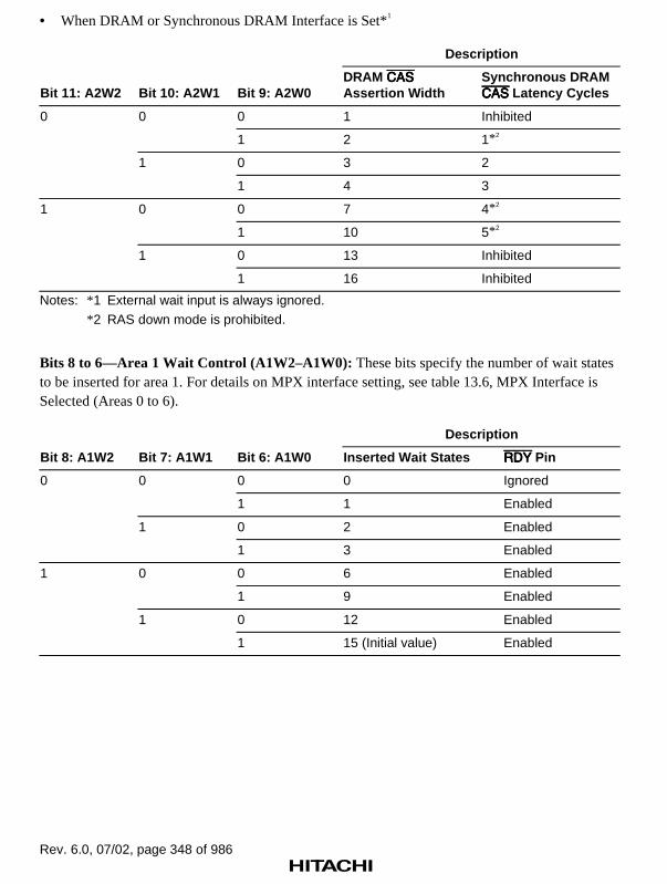
Rev. 6.0, 07/02, page 348 of 986
• When DRAM or Synchronous DRAM Interface is Set*1
Description
Bit 11: A2W2 Bit 10: A2W1 Bit 9: A2W0DRAM CASCASCASCASAssertion Width
Synchronous DRAMCASCASCASCAS Latency Cycles
0 0 0 1 Inhibited
1 2 1*2
1 0 3 2
1 4 3
1 0 0 7 4*2
1 10 5*2
1 0 13 Inhibited
1 16 Inhibited
Notes: *1 External wait input is always ignored.
*2 RAS down mode is prohibited.
Bits 8 to 6—Area 1 Wait Control (A1W2–A1W0): These bits specify the number of wait statesto be inserted for area 1. For details on MPX interface setting, see table 13.6, MPX Interface isSelected (Areas 0 to 6).
Description
Bit 8: A1W2 Bit 7: A1W1 Bit 6: A1W0 Inserted Wait States RDYRDYRDYRDY Pin
0 0 0 0 Ignored
1 1 Enabled
1 0 2 Enabled
1 3 Enabled
1 0 0 6 Enabled
1 9 Enabled
1 0 12 Enabled
1 15 (Initial value) Enabled

Rev. 6.0, 07/02, page 349 of 986
Bits 5 to 3—Area 0 Wait Control (A0W2 to A0W0): These bits specify the number of waitstates to be inserted for area 0. For details on MPX interface setting, see table 13.6, MPX Interfaceis Selected (Areas 0 to 6).
Description
First Cycle
Bit 5: A0W2 Bit 4: A0W1 Bit 3: A0W0 Inserted Wait States RDYRDYRDYRDY Pin
0 0 0 0 Ignored
1 1 Enabled
1 0 2 Enabled
1 3 Enabled
1 0 0 6 Enabled
1 9 Enabled
1 0 12 Enabled
1 15 (Initial value) Enabled
Bits 2 to 0—Area 0 Burst Pitch (A0B2–A0B0): These bits specify the number of wait states tobe inserted afterwards the second data access in a burst transfer with the burst ROM interfaceselected.
Description
Burst Cycle (Excluding First Cycle)
Bit 2: A0B2 Bit 1: A0B1 Bit 0: A0B0Wait States Inserted fromSecond Data Access Onward RDYRDYRDYRDY Pin
0 0 0 0 Ignored
1 1 Enabled
1 0 2 Enabled
1 3 Enabled
1 0 0 4 Enabled
1 5 Enabled
1 0 6 Enabled
1 7 (Initial value) Enabled

Rev. 6.0, 07/02, page 350 of 986
Table 13.6 MPX Interface is Selected (Areas 0 to 6)
Description
Inserted Wait States
1st Data
AnW2 AnW1 AnW0 Read Write2nd DataOnward RDYRDYRDYRDY Pin
0 0 0 1 0 0 Enabled
1 1 Enabled
1 0 2 2 Enabled
1 3 3 Enabled
1 0 0 1 0 1 Enabled
1 1 Enabled
1 0 2 2 Enabled
1 3 3 Enabled
(n = 6 to 0)

Rev. 6.0, 07/02, page 351 of 986
13.2.7 Wait Control Register 3 (WCR3)
Wait control register 3 (WCR3) is a 32-bit readable/writable register that specifies the cyclesinserted in the setup time from the address until assertion of the write strobe, and the data holdtime from negation of the strobe, for each area. This enables low-speed memory to be connectedwithout using external circuitry.
WCR3 is initialized to H'07777777 by a power-on reset, but is not initialized by a manual reset orin standby mode.
Bit: 31 30 29 28 27 26 25 24
Bit name: — — — — — A6S0 A6H1 A6H0
Initial value: 0 0 0 0 0 1 1 1
R/W: R R R R R R/W R/W R/W
Bit: 23 22 21 20 19 18 17 16
Bit name: — A5S0 A5H1 A5H0 A4RDH* A4S0 A4H1 A4H0
Initial value: 0 1 1 1 0 1 1 1
R/W: R R/W R/W R/W R/W* R/W R/W R/W
Bit: 15 14 13 12 11 10 9 8
Bit name: — A3S0 A3H1 A3H0 — A2S0 A2H1 A2H0
Initial value: 0 1 1 1 0 1 1 1
R/W: R R/W R/W R/W R R/W R/W R/W
Bit: 7 6 5 4 3 2 1 0
Bit name: A1RDH* A1S0 A1H1 A0H0 — A0S0 A0H1 A0H0
Initial value: 0 1 1 1 0 1 1 1
R/W: R/W* R/W R/W R/W R R/W R/W R/W
Note: * SH7750R only
Bits 31 to 27, 23, 19*, 15, 11, 7*, and 3—Reserved: These bits are always read as 0, and shouldonly be written with 0.
Note: * SH7750R only

Rev. 6.0, 07/02, page 352 of 986
Bit 4n + 2—Area n (6 to 0) Write Strobe Setup Time (AnS0): Specifies the number of cyclesinserted in the setup time from the address until assertion of the read/write strobe. Valid only forSRAM interface, byte control SRAM interface, and burst ROM interface.
Bit 4n + 2: AnS0 Waits Inserted in Setup
0 0
1 1 (Initial value)
(n = 6 to 0)
Bits 4n + 1 and 4n—Area n (6 to 0) Data Hold Time (AnH1, AnH0): When writing, these bitsspecify the number of cycles to be inserted in the hold time from negation of the write strobe.When reading, they specify the number of cycles to be inserted in the hold time from the datasampling timing. Valid only for SRAM interface, byte control SRAM interface, and burst ROMinterface.
Bit 4n + 1: AnH1 Bit 4n: AnH0 Waits Inserted in Hold
0 0 0
1 1
1 0 2
1 3 (Initial value)
(n = 6 to 0)
Bits 4n+3 Area n (4 or 1) Read-Strobe Negate Timing (AnRDH) (Setting Only Possible inthe SH7750R): When reading, these bits specify the timing for the negation of read strobe. Thesebits should be cleared to 0 when a byte control SRAM setting is made.
Bit 4n + 3: AnRDH Read-Strobe Negate Timing
0 Negation occurs after insertion of the number of hold wait cycles specifiedby the AnH setting (Initial value)
1 Negation occurs based on the read strobe data sampling timing
(n = 4 or 1)
13.2.8 Memory Control Register (MCR)
The memory control register (MCR) is a 32-bit readable/writable register that specifies RAS andCAS timing and burst control for DRAM and synchronous DRAM (areas 2 and 3), addressmultiplexing, and refresh control. This enables DRAM and synchronous DRAM to be connectedwithout using external circuitry.
MCR is initialized to H'00000000 by a power-on reset, but is not initialized by a manual reset or instandby mode. Bits RASD, MRSET, TRC2–0, TPC2–0, RCD1–0, TRWL2–0, TRAS2–0, BE,SZ1–0, AMXEXT, AMX2–0, and EDOMODE are written in the initialization following a power-
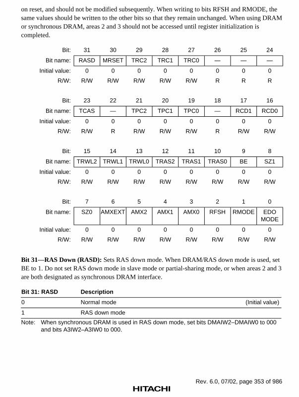
Rev. 6.0, 07/02, page 353 of 986
on reset, and should not be modified subsequently. When writing to bits RFSH and RMODE, thesame values should be written to the other bits so that they remain unchanged. When using DRAMor synchronous DRAM, areas 2 and 3 should not be accessed until register initialization iscompleted.
Bit: 31 30 29 28 27 26 25 24
Bit name: RASD MRSET TRC2 TRC1 TRC0 — — —
Initial value: 0 0 0 0 0 0 0 0
R/W: R/W R/W R/W R/W R/W R R R
Bit: 23 22 21 20 19 18 17 16
Bit name: TCAS — TPC2 TPC1 TPC0 — RCD1 RCD0
Initial value: 0 0 0 0 0 0 0 0
R/W: R/W R R/W R/W R/W R R/W R/W
Bit: 15 14 13 12 11 10 9 8
Bit name: TRWL2 TRWL1 TRWL0 TRAS2 TRAS1 TRAS0 BE SZ1
Initial value: 0 0 0 0 0 0 0 0
R/W: R/W R/W R/W R/W R/W R/W R/W R/W
Bit: 7 6 5 4 3 2 1 0
Bit name: SZ0 AMXEXT AMX2 AMX1 AMX0 RFSH RMODE EDOMODE
Initial value: 0 0 0 0 0 0 0 0
R/W: R/W R/W R/W R/W R/W R/W R/W R/W
Bit 31—RAS Down (RASD): Sets RAS down mode. When DRAM/RAS down mode is used, setBE to 1. Do not set RAS down mode in slave mode or partial-sharing mode, or when areas 2 and 3are both designated as synchronous DRAM interface.
Bit 31: RASD Description
0 Normal mode (Initial value)
1 RAS down mode
Note: When synchronous DRAM is used in RAS down mode, set bits DMAIW2–DMAIW0 to 000and bits A3IW2–A3IW0 to 000.

Rev. 6.0, 07/02, page 354 of 986
Bit 30—Mode Register Set (MRSET): Set when a synchronous DRAM mode register setting isused. See Power-On Sequence in section 13.3.5, Synchronous DRAM Interface.
Bit 30: MRSET Description
0 All-bank precharge (Initial value)
1 Mode register setting
Bits 29 to 27—RAS Precharge Time at End of Refresh (TRC2–TRC0)(Synchronous DRAM: auto- and self-refresh both enabled; DRAM: auto- and self-refresh bothenabled)
Bit 29: TRC2 Bit 28: TRC1 Bit 27: TRC0RAS Precharge IntervalImmediately after Refresh
0 0 0 0 (Initial value)
1 3
1 0 6
1 9
1 0 0 12
1 15
1 0 18
1 21
Bits 26 to 24, 22, and 18—Reserved: These bits are always read as 0, and should only be writtenwith 0.
Bit 23—CAS Negation Period (TCAS): This bit is valid only when DRAM interface is set.
Bit 23: TCAS CAS Negation Period
0 1 (Initial value)
1 2

Rev. 6.0, 07/02, page 355 of 986
Bits 21 to 19—RAS Precharge Period (TPC2–TPC0): When the DRAM interface is set, thesebits specify the minimum number of cycles until RAS is asserted again after being negated. Whenthe synchronous DRAM interface is set, these bits specify the minimum number of cycles until thenext bank active command is output after precharging.
RAS Precharge Interval
Bit 21: TPC2 Bit 20: TPC1 Bit 19: TPC0 DRAM Synchronous DRAM
0 0 0 0 1* (Initial value)
1 1 2
1 0 2 3
1 3 4*
1 0 0 4 5*
1 5 6*
1 0 6 7*
1 7 8*
Note: * Inhibited in RAS down mode.
Bits 17 and 16—RAS-CAS Delay (RCD1, RCD0): When the DRAM interface is set, these bitsset the RAS-CAS assertion delay time. When the synchronous DRAM interface is set, these bitsset the bank active-read/write command delay time.
Description
Bit 17: RCD1 Bit 16: RCD0 DRAM Synchronous DRAM
0 0 2 cycles Reserved (Setting prohibited)
1 3 cycles 2 cycles
1 0 4 cycles 3 cycles
1 5 cycles 4 cycles*
Note: * Inhibited in RAS down mode.
Bits 15 to 13—Write Precharge Delay (TRWL2–TRWL0): These bits set the synchronousDRAM write precharge delay time. In auto-precharge mode, they specify the time until the nextbank active command is issued after a write cycle. After a write cycle, the next active command isnot issued for a period of TPC + TRWL. In RAS down mode, they specify the time until the nextprecharge command is issued. After a write cycle, the next precharge command is not issued for aperiod of TRWL. This setting is valid only when synchronous DRAM interface is set.
For the setting values and delay time when no command is issued, refer to section 22.3.3, BusTiming.

Rev. 6.0, 07/02, page 356 of 986
Bit 15: TRWL2 Bit 14: TRWL1 Bit 13: TRWL0 Write Precharge ACT Delay Time
0 0 0 1 (Initial value)
1 2
1 0 3*
1 4*
1 0 0 5*
1 Reserved (Setting prohibited)
1 0 Reserved (Setting prohibited)
1 Reserved (Setting prohibited)
Note: * Inhibited in RAS down mode.
Bits 12 to 10—CAS-Before-RAS Refresh RASRASRASRAS Assertion Period (TRAS2–TRAS0): When theDRAM interface is set, these bits set the RAS assertion period in CAS-before-RAS refreshing.When the synchronous DRAM interface is set, the bank active command is not issued for a periodof TRC* + TRAS after an auto-refresh command is issued.
Note: * Bits 29 to 27: RAS precharge interval at end of refresh.
Bit 12: TRAS2 Bit 11: TRAS1 Bit 10: TRAS0RASRASRASRAS/DRAMAssertion Period
CommandInterval afterSynchronousDRAM Refresh
0 0 0 2 4 + TRC*(Initial value)
1 3 5 + TRC
1 0 4 6 + TRC
1 5 7 + TRC
1 0 0 6 8 + TRC
1 7 9 + TRC
1 0 8 10 + TRC
1 9 11 + TRC
Note: * Bits 29 to 27: RAS precharge interval at end of refresh.
Bit 9—Burst Enable (BE): Specifies whether burst access is performed on DRAM interface. Insynchronous DRAM access, burst access is always performed regardless of the specification ofthis bit. The DRAM transfer mode depends on EDOMODE.
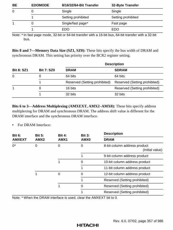
Rev. 6.0, 07/02, page 357 of 986
BE EDOMODE 8/16/32/64-Bit Transfer 32-Byte Transfer
0 0 Single Single
1 Setting prohibited Setting prohibited
1 0 Single/fast page* Fast page
1 EDO EDO
Note: * In fast page mode, 32-bit or 64-bit transfer with a 16-bit bus, 64-bit transfer with a 32-bitbus.
Bits 8 and 7—Memory Data Size (SZ1, SZ0): These bits specify the bus width of DRAM andsynchronous DRAM. This setting has priority over the BCR2 register setting.
Description
Bit 8: SZ1 Bit 7: SZ0 DRAM SDRAM
0 0 64 bits 64 bits
1 Reserved (Setting prohibited) Reserved (Setting prohibited)
1 0 16 bits Reserved (Setting prohibited)
1 32 bits 32 bits
Bits 6 to 3—Address Multiplexing (AMXEXT, AMX2–AMX0): These bits specify addressmultiplexing for DRAM and synchronous DRAM. The address shift value is different for theDRAM interface and the synchronous DRAM interface.
• For DRAM Interface:
DescriptionBit 6:AMXEXT
Bit 5:AMX2
Bit 4:AMX1
Bit 3:AMX0 DRAM
0* 0 0 0 8-bit column address product(Initial value)
1 9-bit column address product
1 0 10-bit column address product
1 11-bit column address product
1 0 0 12-bit column address product
1 Reserved (Setting prohibited)
1 0 Reserved (Setting prohibited)
1 Reserved (Setting prohibited)
Note: * When the DRAM interface is used, clear the AMXEXT bit to 0.

Rev. 6.0, 07/02, page 358 of 986
• For Synchronous DRAM Interface:
AMX AMXEXT SZ Example of Synchronous DRAM BANK*4
0 0 64 (16M: 512k × 16 bits × 2) × 4 a[22]*1
32 (16M: 512k × 16 bits × 2) × 2 a[21]*1
1 64 (16M: 512k × 16 bits × 2) × 4 a[21]*1
32 (16M: 512k × 16 bits × 2) × 2 a[20]*1
1 0 64 (16M: 1M × 8 bits × 2) × 8 a[23]*1
32 (16M: 1M × 8 bits × 2) × 4 a[22]*1
1 64 (16M: 1M × 8 bits × 2) × 8 a[22]*1
32 (16M: 1M × 8 bits × 2) × 4 a[21]*1
2 — 64 (64M: 1M × 16 bits × 4) × 4 a[24:23]*1
32 (64M: 1M × 16 bits × 4) × 2 a[23:22]*1
3 — 64 (64M: 2M × 8 bits × 4) × 8 a[25:24]*1
32 (64M: 2M × 8 bits × 4) × 4 a[24:23]*1
4 — 64 (64M: 512k × 32 bits × 4) × 2 a[23:22]*1
32 (64M: 512k × 32 bits × 4) × 1 a[22:21]*1
5 — 64 (64M: 1M × 32 bits × 2) × 2 a[23]*1
32 (64M: 1M × 32 bits × 2) × 1 a[22]*1
6 0 64 (128M: 4M × 8 bits × 4) × 8*2 a[26:25]*1
1 64 (256M: 4M × 16 bits × 4) × 4*2 a[26:25]*1
0 32 (128M: 4M × 8 bits × 4) × 4*3 a[25:24]*1
1 32 (256M: 4M × 16 bits × 4) × 2*3 a[25:24]*1
7 — 64 (16M: 256k × 32 bits × 2) × 2 a[21]*1
32 (16M: 256k × 32 bits × 2) × 1 a[20]*1
Notes: *1 a[*]: Not an address pin but an external address*2 Can only be set in the SH7750R.*3 Can only be set in the SH7750S/SH7750R (Setting prohibited in the SH7750).*4 For details on address multiplexing, refer to appendix F, Synchronous DRAM Address
Multiplexing Tables.
Bit 2—Refresh Control (RFSH): Specifies refresh control. Selects whether refreshing isperformed for DRAM and synchronous DRAM. When the refresh function is not used, the refreshrequest cycle generation timer can be used as an interval timer.
Bit 2: RFSH Description
0 Refreshing is not performed (Initial value)
1 Refreshing is performed

Rev. 6.0, 07/02, page 359 of 986
Bit 1—Refresh Mode (RMODE): Specifies whether normal refreshing or self-refreshing isperformed when the RFSH bit is set to 1. When the RFSH bit is 1 and this bit is cleared to 0, CAS-before-RAS refreshing or auto-refreshing is performed for DRAM and synchronous DRAM, usingthe cycle set by refresh-related registers RTCNT, RTCOR, and RTCSR. If a refresh request isissued during an external bus cycle, the refresh cycle is executed when the bus cycle ends. Whenthe RFSH bit is 1 and this bit is set to 1, the self-refresh state is set for DRAM and synchronousDRAM, after waiting for the end of any currently executing external bus cycle. All refreshrequests for memory in the self-refresh state are ignored.
Bit 1: RMODE Description
0 CAS-before-RAS refreshing is performed (when RFSH = 1) (Initial value)
1 Self-refreshing is performed (when RFSH = 1)
Bit 0—EDO Mode (EDOMODE): Used to specify the data sampling timing for data reads whenusing EDO mode DRAM interface. The setting of this bit does not affect the operation timing ofmemory other than DRAM. Set this bit to 1 only when DRAM is used.
13.2.9 PCMCIA Control Register (PCR)
The PCMCIA control register (PCR) is a 16-bit readable/writable register that specifies the OEand WE signal assertion/negation timing for the PCMCIA interface connected to areas 5 and 6.The OE and WE signal assertion width is set by the wait control bits in the WCR2 register. Fordetails of access to PCMCIA, see section 13.3.7, PCMCIA Interface.
PCR is initialized to H'0000 by a power-on reset, but is not initialized by a manual reset or instandby mode.
Bit: 15 14 13 12 11 10 9 8
Bit name: A5PCW1 A5PCW0 A6PCW1 A6PCW0 A5TED2 A5TED1 A5TED0 A6TED2
Initial value: 0 0 0 0 0 0 0 0
R/W: R/W R/W R/W R/W R/W R/W R/W R/W
Bit: 7 6 5 4 3 2 1 0
Bit name: A6TED1 A6TED0 A5TEH2 A5TEH1 A5TEH0 A6TEH2 A6TEH1 A6TEH0
Initial value: 0 0 0 0 0 0 0 0
R/W: R/W R/W R/W R/W R/W R/W R/W R/W

Rev. 6.0, 07/02, page 360 of 986
Bits 15 and 14—PCMCIA Wait (A5PCW1, A5PCW0): These bits specify the number of waitsto be added to the number of waits specified by WCR2 in a low-speed PCMCIA wait cycle. Thesetting of these bits is selected when the PCMCIA interface access TC bit is cleared to 0.
Bit 15: A5PCW1 Bit 14: A5PCW0 Waits Inserted
0 0 0 (Initial value)
1 15
1 0 30
1 50
Bits 13 and 12—PCMCIA Wait (A6PCW1, A6PCW0): These bits specify the number of waitsto be added to the number of waits specified by WCR2 in a low-speed PCMCIA wait cycle. Thesetting of these bits is selected when the PCMCIA interface access TC bit is set to 1.
Bit 13: A6PCW1 Bit 12: A6PCW0 Waits Inserted
0 0 0 (Initial value)
1 15
1 0 30
1 50
Bits 11 to 9—Address-OEOEOEOE/WEWEWEWE Assertion Delay (A5TED2–A5TED0): These bits set the delaytime from address output to OE/WE assertion on the connected PCMCIA interface. The setting ofthese bits is selected when the PCMCIA interface access TC bit is cleared to 0.
Bit 11: A5TED2 Bit 10: A5TED1 Bit 9: A5TED0 Waits Inserted
0 0 0 0 (Initial value)
1 1
1 0 2
1 3
1 0 0 6
1 9
1 0 12
1 15

Rev. 6.0, 07/02, page 361 of 986
Bits 8 to 6—Address-OEOEOEOE/WEWEWEWE Assertion Delay (A6TED2–A6TED0): These bits set the delaytime from address output to OE/WE assertion on the connected PCMCIA interface. The setting ofthese bits is selected when the PCMCIA interface access TC bit is set to 1.
Bit 8: A6TED2 Bit 7: A6TED1 Bit 6: A6TED0 Waits Inserted
0 0 0 0 (Initial value)
1 1
1 0 2
1 3
1 0 0 6
1 9
1 0 12
1 15
Bits 5 to 3—OEOEOEOE/WEWEWEWE Negation-Address Delay (A5TEH2–A5TEH0): These bits set the addresshold delay time from OE/WE negation in a write on the connected PCMCIA interface or in an I/Ocard read. The setting of these bits is selected when the PCMCIA interface access TC bit is clearedto 0.
Bit 5: A5TEH2 Bit 4: A5TEH1 Bit 3: A5TEH0 Waits Inserted
0 0 0 0 (Initial value)
1 1
1 0 2
1 3
1 0 0 6
1 9
1 0 12
1 15
Bits 2 to 0—OEOEOEOE/WEWEWEWE Negation-Address Delay (A6TEH2–A6TEH0): These bits set the addresshold delay time from OE/WE negation in a write on the connected PCMCIA interface or in an I/Ocard read. In the case of a memory card read, the address hold delay time from the data samplingtiming is set. The setting of these bits is selected when the PCMCIA interface access TC bit is setto 1.

Rev. 6.0, 07/02, page 362 of 986
Bit 2: A6TEH2 Bit 1: A6TEH1 Bit 0: A6TEH0 Waits Inserted
0 0 0 0 (Initial value)
1 1
1 0 2
1 3
1 0 0 6
1 9
1 0 12
1 15
13.2.10 Synchronous DRAM Mode Register (SDMR)
The synchronous DRAM mode register (SDMR) is a write-only virtual 16-bit register that iswritten to via the synchronous DRAM address bus, and sets the mode of the area 2 and area 3synchronous DRAM.
Settings for the SDMR register must be made before accessing synchronous DRAM.
Bit: 15 14 13 12 11 10 9 8
Bit name:
Initial value: — — — — — — — —
R/W: W W W W W W W W
Bit: 7 6 5 4 3 2 1 0
Bit name:
Initial value: — — — — — — — —
R/W: W W W W W W W W
Since the address bus, not the data bus, is used to write to the synchronous DRAM mode register,if the value to be set is “X” and the SDMR register address is “Y”, value “X” is written to thesynchronous DRAM mode register by performing a write to address X + Y. When thesynchronous DRAM bus width is set to 32 bits, as A0 of the synchronous DRAM is connected toA2 of the SH7750 Series, and A1 of the synchronous DRAM is connected to A3 of the SH7750Series, the value actually written to the synchronous DRAM is the value of “X” shifted 2 bits tothe right.

Rev. 6.0, 07/02, page 363 of 986
For example, to write H'0230 to the area 2 SDMR register, arbitrary data is written to addressH'FF900000 (address “Y”) + H'08C0 (value “X”) (= H'FF9008C0). As a result, H'0230 is writtento the SDMR register. The range of value “X” is H'0000 to H'0FFC.
Similarly, to write H'0230 to the area 3 SDMR register, arbitrary data is written to addressH'FF940000 (address “Y”) + H'08C0 (value “X”) (= H'FF9408C0). As a result, H'0230 is writtento the SDMR register. The range of value “X” is H'0000 to H'0FFC.
The lower 16 bits of the address are set in the synchronous DRAM mode register.
When the bus width is 32 bits, the burst length is 4* and 8. When the bus width is 64 bits, the burstlength is fixed at 4. When a setting is made in SDMR, byte-size writes are performed at thefollowing addresses.
Bus Width Burst Length CAS Latency Area 2 Area 3
32 4* 1
2
3
H'FF900048
H'FF900088
H'FF9000C8
H'FF940048
H'FF940088
H'FF9400C8
32 8 1
2
3
H'FF90004C
H'FF90008C
H'FF9000CC
H'FF94004C
H'FF94008C
H'FF9400CC
64 4 1
2
3
H'FF900090
H'FF900110
H'FF900190
H'FF940090
H'FF940110
H'FF940190
For a 32-bit bus:
17 16 15 14 13 12 11 10 9 8 7 6 5 4 3 2 1 0
Address 0 0 0 0 0 0 0 0 0 LMODE2
LMODE1
LMODE0
WT BL2 BL1 BL0
←→10 bits set in case of 32-bit bus width
For a 64-bit bus:
17 16 15 14 13 12 11 10 9 8 7 6 5 4 3 2 1 0
Address 0 0 0 0 0 0 0 0 LMODE2
LMODE1
LMODE0
WT BL2 BL1 BL0
←→10 bits set in case of 64-bit bus width

Rev. 6.0, 07/02, page 364 of 986
LMODE: RAS-CAS latencyBL: Burst lengthWT: Wrap type (0: Sequential)
BL LMODE000: Reserved 000: Reserved001: Reserved 001: 1010: 4 010: 2011: 8 011: 3100: Reserved 100: Reserved101: Reserved 101: Reserved110: Reserved 110: Reserved111: Reserved 111: Reserved
Note: * SH7750R only.
13.2.11 Refresh Timer Control/Status Register (RTCSR)
The refresh timer control/status register (RTCSR) is a 16-bit readable/writable register thatspecifies the refresh cycle and whether interrupts are to be generated.
RTCSR is initialized to H'0000 by a power-on reset, but is not initialized by a manual reset or instandby mode.
Bit: 15 14 13 12 11 10 9 8
Bit name: — — — — — — — —
Initial value: 0 0 0 0 0 0 0 0
R/W: — — — — — — — —
Bit: 7 6 5 4 3 2 1 0
Bit name: CMF CMIE CKS2 CKS1 CKS0 OVF OVIE LMTS
Initial value: 0 0 0 0 0 0 0 0
R/W: R/W R/W R/W R/W R/W R/W R/W R/W
Bits 15 to 8—Reserved: These bits are always read as 0. For the write values, see section 13.2.15,Notes on Accessing Refresh Control Registers.
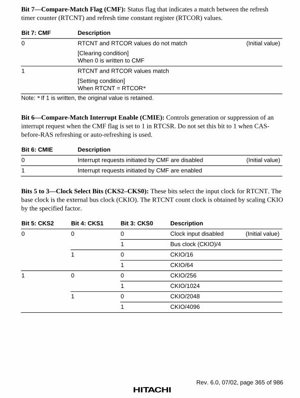
Rev. 6.0, 07/02, page 365 of 986
Bit 7—Compare-Match Flag (CMF): Status flag that indicates a match between the refreshtimer counter (RTCNT) and refresh time constant register (RTCOR) values.
Bit 7: CMF Description
0 RTCNT and RTCOR values do not match (Initial value)
[Clearing condition]When 0 is written to CMF
1 RTCNT and RTCOR values match
[Setting condition]When RTCNT = RTCOR*
Note: * If 1 is written, the original value is retained.
Bit 6—Compare-Match Interrupt Enable (CMIE): Controls generation or suppression of aninterrupt request when the CMF flag is set to 1 in RTCSR. Do not set this bit to 1 when CAS-before-RAS refreshing or auto-refreshing is used.
Bit 6: CMIE Description
0 Interrupt requests initiated by CMF are disabled (Initial value)
1 Interrupt requests initiated by CMF are enabled
Bits 5 to 3—Clock Select Bits (CKS2–CKS0): These bits select the input clock for RTCNT. Thebase clock is the external bus clock (CKIO). The RTCNT count clock is obtained by scaling CKIOby the specified factor.
Bit 5: CKS2 Bit 4: CKS1 Bit 3: CKS0 Description
0 0 0 Clock input disabled (Initial value)
1 Bus clock (CKIO)/4
1 0 CKIO/16
1 CKIO/64
1 0 0 CKIO/256
1 CKIO/1024
1 0 CKIO/2048
1 CKIO/4096

Rev. 6.0, 07/02, page 366 of 986
Bit 2—Refresh Count Overflow Flag (OVF): Status flag that indicates that the number ofrefresh requests indicated by the refresh count register (RFCR) has exceeded the number specifiedby the LMTS bit in RTCSR.
Bit 2: OVF Description
0 RFCR has not overflowed the count limit indicated by LMTS (Initial value)
[Clearing condition]When 0 is written to OVF
1 RFCR has overflowed the count limit indicated by LMTS
[Setting condition]When RFCR overflows the count limit set by LMTS*
Note: * If 1 is written, the original value is retained.
Bit 1—Refresh Count Overflow Interrupt Enable (OVIE): Controls generation or suppressionof an interrupt request when the OVF flag is set to 1 in RTCSR.
Bit 1: OVIE Description
0 Interrupt requests initiated by OVF are disabled (Initial value)
1 Interrupt requests initiated by OVF are enabled
Bit 0—Refresh Count Overflow Limit Select (LMTS): Specifies the count limit to be comparedwith the refresh count indicated by the refresh count register (RFCR). If the RFCR register valueexceeds the value specified by LMTS, the OVF flag is set.
Bit 0: LMTS Description
0 Count limit is 1024 (Initial value)
1 Count limit is 512

Rev. 6.0, 07/02, page 367 of 986
13.2.12 Refresh Timer Counter (RTCNT)
The refresh timer counter (RTCNT) is an 8-bit readable/writable counter that is incremented bythe input clock (selected by bits CKS2–CKS0 in the RTCSR register). When the RTCNT countervalue matches the RTCOR register value, the CMF bit is set in the RTCSR register and theRTCNT counter is cleared.
RTCNT is initialized to H'0000 by a power-on reset, but continues to count when a manual reset isperformed. In standby mode, RTCNT is not initialized, and retains its contents.
Bit: 15 14 13 12 11 10 9 8
Bit name: — — — — — — — —
Initial value: 0 0 0 0 0 0 0 0
R/W: — — — — — — — —
Bit: 7 6 5 4 3 2 1 0
Bit name:
Initial value: 0 0 0 0 0 0 0 0
R/W: R/W R/W R/W R/W R/W R/W R/W R/W

Rev. 6.0, 07/02, page 368 of 986
13.2.13 Refresh Time Constant Register (RTCOR)
The refresh time constant register (RTCOR) is a readable/writable register that specifies the upperlimit of the RTCNT counter. The RTCOR register and RTCNT counter values (lower 8 bits) areconstantly compared, and when they match the CMF bit is set in the RTCSR register and theRTCNT counter is cleared to 0. If the refresh bit (RFSH) has been set to 1 in the memory controlregister (MCR) and CAS-before-RAS has been selected as the refresh mode, a memory refreshcycle is generated when the CMF bit is set.
RTCOR is initialized to H'0000 by a power-on reset, but is not initialized, and retains its contents,in a manual reset and in standby mode.
Bit: 15 14 13 12 11 10 9 8
Bit name: — — — — — — — —
Initial value: 0 0 0 0 0 0 0 0
R/W: — — — — — — — —
Bit: 7 6 5 4 3 2 1 0
Bit name:
Initial value: 0 0 0 0 0 0 0 0
R/W: R/W R/W R/W R/W R/W R/W R/W R/W

Rev. 6.0, 07/02, page 369 of 986
13.2.14 Refresh Count Register (RFCR)
The refresh count register (RFCR) is a 10-bit readable/writable counter that counts the number ofrefreshes by being incremented each time the RTCOR register and RTCNT counter values match.If the RFCR register value exceeds the count limit specified by the LMTS bit in the RTCSRregister, the OVF flag is set in the RTCSR register and the RFCR register is cleared.
RFCR is initialized to H'0000 by a power-on reset, but is not initialized, and retains its contents, ina manual reset and in standby mode.
Bit: 15 14 13 12 11 10 9 8
Bit name: — — — — — —
Initial value: 0 0 0 0 0 0 0 0
R/W: — — — — — — R/W R/W
Bit: 7 6 5 4 3 2 1 0
Bit name:
Initial value: 0 0 0 0 0 0 0 0
R/W: R/W R/W R/W R/W R/W R/W R/W R/W
13.2.15 Notes on Accessing Refresh Control Registers
When the refresh timer control/status register (RTCSR), refresh timer counter (RTCNT), refreshtime constant register (RTCOR), and refresh count register (RFCR) are written to, a special codeis added to the data to prevent inadvertent rewriting in the event of program runaway, etc. Thefollowing procedures should be used for read/write operations.
Writing to RTCSR, RTCNT, RTCOR, and RFCR: A word transfer instruction must always beused when writing to RTCSR, RTCNT, RTCOR, or RFCR. A write cannot be performed with abyte transfer instruction.
When writing to RTCSR, RTCNT, or RTCOR, set B'10100101 in the upper byte and the writedata in the lower byte, as shown in figure 13.5. When writing to RFCR, set B'101001 in the 6 bitsstarting from the MSB in the upper byte, and the write data in the remaining bits.

Rev. 6.0, 07/02, page 370 of 986
15 14 13 12 11 10 9 8
1 0 1 0 0 1 0 1
7 6 5 4 3 2 1 0
15 14 13 12 11 10 9 8
1 0 1 0 0 1
7 6 5 4 3 2 1 0
Write data
Write data
RTCSR,RTCNT,RTCOR
RFCR
Figure 13.5 Writing to RTCSR, RTCNT, RTCOR, and RFCR
Reading RTCSR, RTCNT, RTCOR, and RFCR: A 16-bit access must always be used whenreading RTCSR, RTCNT, RTCOR, or RFCR. Undefined bits are read as 0.
13.3 Operation
13.3.1 Endian/Access Size and Data Alignment
The SH7750 Series supports both big-endian mode, in which the most significant byte (MSByte)is at the 0 address end in a string of byte data, and little-endian mode, in which the least significantbyte (LSByte) is at the 0 address end. The mode is set by means of the MD5 external pin in apower-on reset by the RESET pin, big-endian mode being set if the MD5 pin is low, and little-endian mode if it is high.
A data bus width of 8, 16, 32, or 64 bits can be selected for normal memory, 16, 32, or 64 bits forDRAM, 32 or 64 bits for synchronous DRAM, and 8 or 16 bits for the PCMCIA interface. Dataalignment is carried out according to the data bus width and endian mode of each device. If thedata bus width is smaller than the access size, a number of bus cycles will be generatedautomatically until the access size is reached. In this case, address incrementing is performedautomatically according to the bus width as access is performed. For example, if longword accessis performed in an 8-bit bus width area using the SRAM interface, four accesses are executed,with the address automatically incremented by 1 each time. In 32-byte transfer, a total of 32 bytesof data are transferred consecutively according to the set bus width. The first access is performedon the data for which there was an access request, and the remaining accesses are performed on32-byte boundary data using wraparound. Bus release or refresh operations are not performedbetween these transfers. Data alignment and data length conversion between the differentinterfaces is performed automatically. Quadword access is used only in transfer by the DMAC.
The relationship between the endian mode, device data length, and access unit, is shown in tables13.7 to 13.14.

Rev. 6.0, 07/02, page 371 of 986
Data Configuration
MSB LSB
Byte Data 7 to 0
MSB LSB
Word Data 15 to 8 Data 7 to 0
MSB LSB
Longword Data 31 to 24 Data 23 to 16 Data 15 to 8 Data 7 to 0
MSB LSB
Quadword Data63 to 56
Data55 to 48
Data47 to 40
Data39 to 32
Data31 to 24
Data23 to 16
Data15 to 8
Data7 to 0

Rev. 6.0, 07/02, page 372 of 986
Table 13.7 (1) 64-Bit External Device/Big-Endian Access and Data Alignment
Operation Data Bus
AccessSize Address No. D63–56 D55–48 D47–40 D39–32 D31–24 D23–16 D15–8 D7–0
Byte 8n 1 Data7–0
— — — — — — —
8n+1 1 — Data7–0
— — — — — —
8n+2 1 — — Data7–0
— — — — —
8n+3 1 — — — Data7–0
— — — —
8n+4 1 — — — — Data7–0
— — —
8n+5 1 — — — — — Data7–0
— —
8n+6 1 — — — — — — Data7–0
—
8n+7 1 — — — — — — — Data7–0
Word 8n 1 Data15–8
Data7–0
— — — — — —
8n+2 1 — — Data15–8
Data7–0
— — — —
8n+4 1 — — — — Data15–8
Data7–0
— —
8n+6 1 — — — — — — Data15–8
Data7–0
Long-word
8n 1 Data31–24
Data23–16
Data15–8
Data7–0
— — — —
8n+4 1 — — — — Data31–24
Data23–16
Data15–8
Data7–0
Quad-word
8n 1 Data63–56
Data55–48
Data47–40
Data39–32
Data31–24
Data23–16
Data15–8
Data7–0

Rev. 6.0, 07/02, page 373 of 986
Table 13.7 (2) 64-Bit External Device/Big-Endian Access and Data Alignment
Operation Strobe Signals
AccessSize Address No.
WE7WE7WE7WE7,CAS7CAS7CAS7CAS7,DQM7
WE6WE6WE6WE6,CAS6CAS6CAS6CAS6,DQM6
WE5WE5WE5WE5,CAS5CAS5CAS5CAS5,DQM5
WE4WE4WE4WE4,CAS4CAS4CAS4CAS4,DQM4
WE3WE3WE3WE3,CAS3CAS3CAS3CAS3,DQM3
WE2WE2WE2WE2,CAS2CAS2CAS2CAS2,DQM2
WE1WE1WE1WE1,CAS1CAS1CAS1CAS1,DQM1
WE0WE0WE0WE0,CAS0CAS0CAS0CAS0,DQM0
Byte 8n 1 Asserted
8n+1 1 Asserted
8n+2 1 Asserted
8n+3 1 Asserted
8n+4 1 Asserted
8n+5 1 Asserted
8n+6 1 Asserted
8n+7 1 Asserted
Word 8n 1 Asserted Asserted
8n+2 1 Asserted Asserted
8n+4 1 Asserted Asserted
8n+6 1 Asserted Asserted
8n 1 Asserted Asserted Asserted AssertedLong-word
8n+4 1 Asserted Asserted Asserted Asserted
Quad-word
8n 1 Asserted Asserted Asserted Asserted Asserted Asserted Asserted Asserted

Rev. 6.0, 07/02, page 374 of 986
Table 13.8 32-Bit External Device/Big-Endian Access and Data Alignment
Operation Data Bus Strobe Signals
AccessSize Address No. D31–D24 D23–D16 D15–D8 D7–D0
WE3WE3WE3WE3,CAS3CAS3CAS3CAS3,DQM3
WE2WE2WE2WE2,CAS2CAS2CAS2CAS2,DQM2
WE1WE1WE1WE1,CAS1CAS1CAS1CAS1,DQM1
WE0WE0WE0WE0,CAS0CAS0CAS0CAS0,DQM0
Byte 4n 1 Data7–0
— — — Asserted
4n+1 1 — Data7–0
— — Asserted
4n+2 1 — — Data7–0
— Asserted
4n+3 1 — — — Data7–0
Asserted
Word 4n 1 Data15–8
Data7–0
— — Asserted Asserted
4n+2 1 — — Data15–8
Data7–0
Asserted Asserted
Long-word
4n 1 Data31–24
Data23–16
Data15–8
Data7–0
Asserted Asserted Asserted Asserted
Quad-word
8n 1 Data63–56
Data55–48
Data47–40
Data39–32
Asserted Asserted Asserted Asserted
8n+4 2 Data31–24
Data23–16
Data15–8
Data7–0
Asserted Asserted Asserted Asserted

Rev. 6.0, 07/02, page 375 of 986
Table 13.9 16-Bit External Device/Big-Endian Access and Data Alignment
Operation Data Bus Strobe Signals
AccessSize Address No. D31–D24 D23–D16 D15–D8 D7–D0
WE3WE3WE3WE3,CAS3CAS3CAS3CAS3,DQM3
WE2WE2WE2WE2,CAS2CAS2CAS2CAS2,DQM2
WE1WE1WE1WE1,CAS1CAS1CAS1CAS1,DQM1
WE0WE0WE0WE0,CAS0CAS0CAS0CAS0,DQM0
Byte 2n 1 — — Data7–0
— Asserted
2n+1 1 — — — Data7–0
Asserted
Word 2n 1 — — Data15–8
Data7–0
Asserted Asserted
Long-word
4n 1 — — Data31–24
Data23–16
Asserted Asserted
4n+2 2 — — Data15–8
Data7–0
Asserted Asserted
Quad-word
8n 1 — — Data63–56
Data55–48
Asserted Asserted
8n+2 2 — — Data47–40
Data39–32
Asserted Asserted
8n+4 3 — — Data31–24
Data23–16
Asserted Asserted
8n+6 4 — — Data15–8
Data7–0
Asserted Asserted

Rev. 6.0, 07/02, page 376 of 986
Table 13.10 8-Bit External Device/Big-Endian Access and Data Alignment
Operation Data Bus Strobe Signals
AccessSize Address No. D31–D24 D23–D16 D15–D8 D7–D0
WE3WE3WE3WE3,CAS3CAS3CAS3CAS3,DQM3
WE2WE2WE2WE2,CAS2CAS2CAS2CAS2,DQM2
WE1WE1WE1WE1,CAS1CAS1CAS1CAS1,DQM1
WE0WE0WE0WE0,CAS0CAS0CAS0CAS0,DQM0
Byte n 1 — — — Data7–0
Asserted
Word 2n 1 — — — Data15–8
Asserted
2n+1 2 — — — Data7–0
Asserted
Long-word
4n 1 — — — Data31–24
Asserted
4n+1 2 — — — Data23–16
Asserted
4n+2 3 — — — Data15–8
Asserted
4n+3 4 — — — Data7–0
Asserted
Quad-word
8n 1 — — — Data63–56
Asserted
8n+1 2 — — — Data55–48
Asserted
8n+2 3 — — — Data47–40
Asserted
8n+3 4 — — — Data39–32
Asserted
8n+4 5 — — — Data31–24
Asserted
8n+5 6 — — — Data23–16
Asserted
8n+6 7 — — — Data15–8
Asserted
8n+7 8 — — — Data7–0
Asserted

Rev. 6.0, 07/02, page 377 of 986
Table 13.11 (1) 64-Bit External Device/Little-Endian Access and Data Alignment
Operation Data Bus
AccessSize Address No. D63–56 D55–48 D47–40 D39–32 D31–24 D23–16 D15–8 D7–0
Byte 8n 1 — — — — — — — Data7–0
8n+1 1 — — — — — — Data7–0
—
8n+2 1 — — — — — Data7–0
— —
8n+3 1 — — — — Data7–0
— — —
8n+4 1 — — — Data7–0
— — — —
8n+5 1 — — Data7–0
— — — — —
8n+6 1 — Data7–0
— — — — — —
8n+7 1 Data7–0
— — — — — — —
Word 8n 1 — — — — — — Data15–8
Data7–0
8n+2 1 — — Data15–8
Data7–0
— —
8n+4 1 — — Data15–8
Data7–0
— — — —
8n+6 1 Data15–8
Data7–0
— — — — — —
Long-word
8n 1 — — — — Data31–24
Data23–16
Data15–8
Data7–0
8n+4 1 Data31–24
Data23–16
Data15–8
Data7–0
— — — —
Quad-word
8n 1 Data63–56
Data55–48
Data47–40
Data39–32
Data31–24
Data23–16
Data15–8
Data7–0

Rev. 6.0, 07/02, page 378 of 986
Table 13.11 (2) 64-Bit External Device/Little-Endian Access and Data Alignment
Operation Strobe Signals
AccessSize Address No.
WE7WE7WE7WE7,CAS7CAS7CAS7CAS7,DQM7
WE6WE6WE6WE6,CAS6CAS6CAS6CAS6,DQM6
WE5WE5WE5WE5,CAS5CAS5CAS5CAS5,DQM5
WE4WE4WE4WE4,CAS4CAS4CAS4CAS4,DQM4
WE3WE3WE3WE3,CAS3CAS3CAS3CAS3,DQM3
WE2WE2WE2WE2,CAS2CAS2CAS2CAS2,DQM2
WE1WE1WE1WE1,CAS1CAS1CAS1CAS1,DQM1
WE0WE0WE0WE0,CAS0CAS0CAS0CAS0,DQM0
Byte 8n 1 Asserted
8n+1 1 Asserted
8n+2 1 Asserted
8n+3 1 Asserted
8n+4 1 Asserted
8n+5 1 Asserted
8n+6 1 Asserted
8n+7 1 Asserted
Word 8n 1 Asserted Asserted
8n+2 1 Asserted Asserted
8n+4 1 Asserted Asserted
8n+6 1 Asserted Asserted
8n 1 Asserted Asserted Asserted AssertedLong-word
8n+4 1 Asserted Asserted Asserted Asserted
Quad-word
8n 1 Asserted Asserted Asserted Asserted Asserted Asserted Asserted Asserted

Rev. 6.0, 07/02, page 379 of 986
Table 13.12 32-Bit External Device/Little-Endian Access and Data Alignment
Operation Data Bus Strobe Signals
AccessSize Address No. D31–D24 D23–D16 D15–D8 D7–D0
WE3WE3WE3WE3,CAS3CAS3CAS3CAS3,DQM3
WE2WE2WE2WE2,CAS2CAS2CAS2CAS2,DQM2
WE1WE1WE1WE1,CAS1CAS1CAS1CAS1,DQM1
WE0WE0WE0WE0,CAS0CAS0CAS0CAS0,DQM0
Byte 4n 1 — — Data7–0
Asserted
4n+1 1 — — Data7–0
— Asserted
4n+2 1 — Data7–0
— — Asserted
4n+3 1 Data7–0
— — — Asserted
Word 4n 1 — — Data15–8
Data7–0
Asserted Asserted
4n+2 1 Data15–8
Data7–0
— — Asserted Asserted
Long-word
4n 1 Data31–24
Data23–16
Data15–8
Data7–0
Asserted Asserted Asserted Asserted
Quad-word
8n 1 Data31–24
Data23–16
Data15–8
Data7–0
Asserted Asserted Asserted Asserted
8n+4 2 Data63–56
Data55–48
Data47–40
Data39–32
Asserted Asserted Asserted Asserted

Rev. 6.0, 07/02, page 380 of 986
Table 13.13 16-Bit External Device/Little-Endian Access and Data Alignment
Operation Data Bus Strobe Signals
AccessSize Address No. D31–D24 D23–D16 D15–D8 D7–D0
WE3WE3WE3WE3,CAS3CAS3CAS3CAS3,DQM3
WE2WE2WE2WE2,CAS2CAS2CAS2CAS2,DQM2
WE1WE1WE1WE1,CAS1CAS1CAS1CAS1,DQM1
WE0WE0WE0WE0,CAS0CAS0CAS0CAS0,DQM0
Byte 2n 1 — — — Data7–0
Asserted
2n+1 1 — — Data7–0
— Asserted
Word 2n 1 — — Data15–8
Data7–0
Asserted Asserted
Long-word
4n 1 — — Data15–8
Data7–0
Asserted Asserted
4n+2 2 — — Data31–24
Data23–16
Asserted Asserted
Quad-word
8n 1 — — Data15–8
Data7–0
Asserted Asserted
8n+2 2 — — Data31–24
Data23–16
Asserted Asserted
8n+4 3 — — Data47–40
Data39–32
Asserted Asserted
8n+6 4 — — Data63–56
Data55–48
Asserted Asserted

Rev. 6.0, 07/02, page 381 of 986
Table 13.14 8-Bit External Device/Little-Endian Access and Data Alignment
Operation Data Bus Strobe Signals
AccessSize Address No. D31–D24 D23–D16 D15–D8 D7–D0
WE3WE3WE3WE3,CAS3CAS3CAS3CAS3,DQM3
WE2WE2WE2WE2,CAS2CAS2CAS2CAS2,DQM2
WE1WE1WE1WE1,CAS1CAS1CAS1CAS1,DQM1
WE0WE0WE0WE0,CAS0CAS0CAS0CAS0,DQM0
Byte n 1 — — — Data7–0
Asserted
Word 2n 1 — — — Data7–0
Asserted
2n+1 2 — — — Data15–8
Asserted
Long-word
4n 1 — — — Data7–0
Asserted
4n+1 2 — — — Data15–8
Asserted
4n+2 3 — — — Data23–16
Asserted
4n+3 4 — — — Data31–24
Asserted
Quad-word
8n 1 — — — Data7–0
Asserted
8n+1 2 — — — Data15–8
Asserted
8n+2 3 — — — Data23–16
Asserted
8n+3 4 — — — Data31–24
Asserted
8n+4 5 — — — Data39–32
Asserted
8n+5 6 — — — Data47–40
Asserted
8n+6 7 — — — Data55–48
Asserted
8n+7 8 — — — Data63–56
Asserted
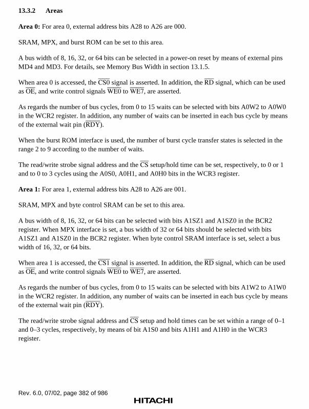
Rev. 6.0, 07/02, page 382 of 986
13.3.2 Areas
Area 0: For area 0, external address bits A28 to A26 are 000.
SRAM, MPX, and burst ROM can be set to this area.
A bus width of 8, 16, 32, or 64 bits can be selected in a power-on reset by means of external pinsMD4 and MD3. For details, see Memory Bus Width in section 13.1.5.
When area 0 is accessed, the CS0 signal is asserted. In addition, the RD signal, which can be usedas OE, and write control signals WE0 to WE7, are asserted.
As regards the number of bus cycles, from 0 to 15 waits can be selected with bits A0W2 to A0W0in the WCR2 register. In addition, any number of waits can be inserted in each bus cycle by meansof the external wait pin (RDY).
When the burst ROM interface is used, the number of burst cycle transfer states is selected in therange 2 to 9 according to the number of waits.
The read/write strobe signal address and the CS setup/hold time can be set, respectively, to 0 or 1and to 0 to 3 cycles using the A0S0, A0H1, and A0H0 bits in the WCR3 register.
Area 1: For area 1, external address bits A28 to A26 are 001.
SRAM, MPX and byte control SRAM can be set to this area.
A bus width of 8, 16, 32, or 64 bits can be selected with bits A1SZ1 and A1SZ0 in the BCR2register. When MPX interface is set, a bus width of 32 or 64 bits should be selected with bitsA1SZ1 and A1SZ0 in the BCR2 register. When byte control SRAM interface is set, select a buswidth of 16, 32, or 64 bits.
When area 1 is accessed, the CS1 signal is asserted. In addition, the RD signal, which can be usedas OE, and write control signals WE0 to WE7, are asserted.
As regards the number of bus cycles, from 0 to 15 waits can be selected with bits A1W2 to A1W0in the WCR2 register. In addition, any number of waits can be inserted in each bus cycle by meansof the external wait pin (RDY).
The read/write strobe signal address and CS setup and hold times can be set within a range of 0–1and 0–3 cycles, respectively, by means of bit A1S0 and bits A1H1 and A1H0 in the WCR3register.

Rev. 6.0, 07/02, page 383 of 986
Area 2: For area 2, external address bits A28 to A26 are 010.
SRAM, MPX, DRAM, and synchronous DRAM can be set to this area.
When SRAM interface is set, a bus width of 8, 16, 32, or 64 bits can be selected with bits A2SZ1and A2SZ0 in the BCR2 register. When MPX interface is set, a bus width of 32 or 64 bits shouldbe selected with bits A2SZ1 and A2SZ0 in the BCR2 register. When synchronous DRAMinterface is set, select 32 or 64 bits with the SZ bits in the MCR register. When DRAM isconnected to area 2, select a bus width of 16 or 32 bits with the SZ bits in MCR. For details, seeMemory Bus Width in section 13.1.5.
When area 2 is accessed, the CS2 signal is asserted.
When SRAM interface is set, the RD signal, which can be used as OE, and write control signalsWE0 to WE7, are asserted.
As regards the number of bus cycles, from 0 to 15 waits can be selected with bits A2W2 to A2W0in the WCR2 register. In addition, any number of waits can be inserted in each bus cycle by meansof the external wait pin (RDY).
The read/write strobe signal address and CS setup and hold times can be set within a range of 0–1and 0–3 cycles, respectively, by means of bit A2S0 and bits A2H1 and A2H0 in the WCR3register.
When synchronous DRAM interface is set, the RAS and CAS signals, RD/WR signal, and bytecontrol signals DQM0 to DQM7 are asserted, and address multiplexing is performed. RAS, CAS,and data timing control, and address multiplexing control, can be set using the MCR register.
When DRAM is connected, the RAS2 signal, CAS4 to CAS7 signals, and RD/WR signal areasserted, and address multiplexing is performed. RAS2, CAS, and data timing control, and addressmultiplexing control, can be set using the MCR register.
Area 3: For area 3, external address bits A28 to A26 are 011.
SRAM, MPX, DRAM, and synchronous DRAM can be set to this area.
When SRAM interface is set, a bus width of 8, 16, 32, or 64 bits can be selected with bits A3SZ1and A3SZ0 in the BCR2 register. When MPX interface is set, a bus width of 32 or 64 bits shouldbe selected with bits A3SZ1 and A3SZ0 in the BCR2 register. When DRAM interface is set, 16,32, or 64 bits can be selected with the SZ bits in the MCR register. When synchronous DRAMinterface is set, select 32 or 64 bits with the SZ bits in MCR. For details, see Memory Bus Widthin section 13.1.5.
When area 3 is accessed, the CS3 signal is asserted.

Rev. 6.0, 07/02, page 384 of 986
When SRAM interface is set, the RD signal, which can be used as OE, and write control signalsWE0 to WE7, are asserted.
As regards the number of bus cycles, from 0 to 15 waits can be selected with bits A3W2 to A3W0in the WCR2 register. In addition, any number of waits can be inserted in each bus cycle by meansof the external wait pin (RDY).
The read/write strobe signal address and CS setup and hold times can be set within a range of 0–1and 0–3 cycles, respectively, by means of bit A3S0 and bits A3H1 and A3H0 in the WCR3register.
When synchronous DRAM interface is set, the RAS and CAS signals, RD/WR signal, and bytecontrol signals DQM0 to DQM7 are asserted, and address multiplexing is performed. WhenDRAM interface is set, the RAS signal, CAS0 to CAS7 signals, and RD/WR signal are asserted,and address multiplexing is performed. RAS, CAS, and data timing control, and addressmultiplexing control, can be set using the MCR register.
Area 4: For area 4, external address bits A28 to A26 are 100.
SRAM, MPX, and byte control SRAM can be set to this area.
A bus width of 8, 16, 32, or 64 bits can be selected with bits A4SZ1 and A4SZ0 in the BCR2register. When MPX interface is set, a bus width of 32 or 64 bits should be selected with bitsA4SZ1 and A4SZ0 in the BCR2 register. When byte control SRAM interface is set, select a buswidth of 16, 32, or 64 bits. For details, see Memory Bus Width in section 13.1.5.
When area 4 is accessed, the CS4 signal is asserted, and the RD signal, which can be used as OE,and write control signals WE0 to WE7, are also asserted.
As regards the number of bus cycles, from 0 to 15 waits can be selected with bits A4W2 to A4W0in the WCR2 register. In addition, any number of waits can be inserted in each bus cycle by meansof the external wait pin (RDY).
The read/write strobe signal address and CS setup and hold times can be set within a range of 0–1and 0–3 cycles, respectively, by means of bit A4S0 and bits A4H1 and A4H0 in the WCR3register.

Rev. 6.0, 07/02, page 385 of 986
Area 5: For area 5, external address bits A28 to A26 are 101.
SRAM, MPX, burst ROM, and a PCMCIA interface can be set to this area.
When SRAM interface is set, a bus width of 8, 16, 32, or 64 bits can be selected with bits A5SZ1and A5SZ0 in the BCR2 register. When burst ROM interface is set, a bus width of 8, 16 or 32 bitscan be selected with bits A5SZ1 and A5SZ0 in BCR2. When MPX interface is set, a bus width of32 or 64 bits should be selected with bits A5SZ1 and A5SZ0 in BCR2. When a PCMCIA interfaceis set, either 8 or 16 bits should be selected with bits A5SZ1 and A5SZ0 in BCR2. For details, seeMemory Bus Width in section 13.1.5.
When area 5 set is accessed with SRAM interface set, the CS5 signal is asserted. In addition, theRD signal, which can be used as OE, and write control signals WE0 to WE7, are asserted. When aPCMCIA interface is connected, the CE1A and CE2A signals, the RD signal, which can be usedas OE, and the WE1, WE2, WE3, and WE7 signals, which can be used as WE, ICIORD,ICIOWR, and REG, respectively, are asserted.
As regards the number of bus cycles, from 0 to 15 waits can be selected with bits A5W2 to A5W0in the WCR2 register. In addition, any number of waits can be inserted in each bus cycle by meansof the external wait pin (RDY).
When the burst function is used, the number of burst cycle transfer states is determined in therange 2 to 9 according to the number of waits.
The read/write strobe signal address and CS setup and hold times can be set within a range of 0–1and 0–3 cycles, respectively, by means of bit A5S0 and bits A5H1 and A5H0 in the WCR3register.
When a PCMCIA interface is used, the address/CE1A/CE2A setup and hold times with respect tothe read/write strobe signals can be set in the range of 0 to 15 cycles with bits AnTED1 andAnTED0, and bits AnTEH1 and AnTEH0, in the PCR register. In addition, the number of waitcycles can be set in the range 0 to 50 with bits AnPCW1 and AnPCW0. The number of waits set inPCR is added to the number of waits set in WCR2.

Rev. 6.0, 07/02, page 386 of 986
Area 6: For area 6, external address bits A28 to A26 are 110.
SRAM, MPX, burst ROM, and a PCMCIA interface can be set to this area.
When SRAM interface is set, a bus width of 8, 16, 32, or 64 bits can be selected with bits A6SZ1and A6SZ0 in the BCR2 register. When burst ROM interface is set, a bus width of 8, 16 or 32 bitscan be selected with bits A6SZ1 and A6SZ0 in BCR2. When MPX interface is set, a bus width of32 or 64 bits should be selected with bits A6SZ1 and A6SZ0 in BCR2. When a PCMCIA interfaceis set, either 8 or 16 bits should be selected with bits A6SZ1 and A6SZ0 in BCR2. For details, seeMemory Bus Width in section 13.1.5.
When area 6 is accessed with SRAM interface set, the CS6 signal is asserted. In addition, the RDsignal, which can be used as OE, and write control signals WE0 to WE7, are asserted. When aPCMCIA interface is set, the CE1B and CE2B signals, the RD signal, which can be used as OE,and the WE1, WE2, WE3, and WE7 signals, which can be used as WE, ICIORD, ICIOWR, andREG, respectively, are asserted.
As regards the number of bus cycles, from 0 to 15 waits can be selected with bits A6W2 to A6W0in the WCR2 register. In addition, any number of waits can be inserted in each bus cycle by meansof the external wait pin (RDY).
When the burst function is used, the number of burst cycle transfer states is determined in therange 2 to 9 according to the number of waits.
The read/write strobe signal address and CS setup and hold times can be set within a range of 0–1and 0–3 cycles, respectively, by means of bit A6S0 and bits A6H1 and A6H0 in the WCR3register.
When a PCMCIA interface is used, the address/CE1B/CE2B setup and hold times with respect tothe read/write strobe signals can be set in the range of 0 to 15 cycles with bits AnTED1 andAnTED0, and bits AnTEH1 and AnTEH0, in the PCR register. In addition, the number of waitcycles can be set in the range 0 to 50 with bits AnPCW1 and AnPCW0. The number of waits set inPCR is added to the number of waits set in WCR2.

Rev. 6.0, 07/02, page 387 of 986
13.3.3 SRAM Interface
Basic Timing: The SRAM interface of the SH7750 Series uses strobe signal output inconsideration of the fact that mainly SRAM will be connected. Figure 13.6 shows the basic timingof normal space accesses. A no-wait normal access is completed in two cycles. The BS signal isasserted for one cycle to indicate the start of a bus cycle. The CSn signal is asserted on the T1rising edge, and negated on the next T2 clock rising edge. Therefore, there is no negation period incase of access at minimum pitch.
There is no access size specification when reading. The correct access address is output to theaddress pins (A[25:0]), but since there is no access size specification, 32 bits are always read inthe case of a 32-bit device, and 16 bits in the case of a 16-bit device. When writing, only the WEsignal for the byte to be written is asserted. For details, see section 13.3.1, Endian/Access Size andData Alignment.
In 32-byte transfer, a total of 32 bytes are transferred consecutively according to the set bus width.The first access is performed on the data for which there was an access request, and the remainingaccesses are performed in wrap around mode on the data at the 32-byte boundary. The bus is notreleased during this transfer.

Rev. 6.0, 07/02, page 388 of 986
T1
CKIO
A25–A0
RD/
D63–D0(read)
D63–D0 (write)
T2
DACKn(SA: IO ← memory)
DACKn(SA: IO → memory)
DACKn(DA)
SA: Single address DMADA: Dual address DMA
Note: For DACKn, an example is shown where CHCRn.AL (access level) = 0 for the DMAC.
Figure 13.6 Basic Timing of SRAM Interface

Rev. 6.0, 07/02, page 389 of 986
Figures 13.7, 13.8, 13.9, and 13.10 show examples of connection to 64-, 32-, 16-, and 8-bit datawidth SRAM.
A19–A3
D63–D56
SH7750 Series128k × 8-bit
SRAM
A16–A0
I/O7–I/O0
A16–A0
I/O7–I/O0
A16–A0
I/O7–I/O0
D55–D48
D47–D40
D39–D32
D31–D24
D23–D16
D15–D8
D7–D0
A16–A0
I/O7–I/O0
A16–A0
I/O7–I/O0
A16–A0
I/O7–I/O0
A16–A0
I/O7–I/O0
A16–A0
I/O7–I/O0
Figure 13.7 Example of 64-Bit Data Width SRAM Connection

Rev. 6.0, 07/02, page 390 of 986
••••
••••
••••
••••
••••
A16
A0
I/O7
I/O0
••••
••••
••••
••••
A18
A2
D31
D24
D23
D16
D15
D8
D7
D0
SH7750 Series128k × 8-bit
SRAM
••••
A16
A0
I/O7
I/O0
••••
••••
••••
••••
••••
••••
A16
A0
I/O7
I/O0
••••
••••
••••
••••
A16
A0
I/O7
I/O0
••••
••••
••••
••••
••••
••••
Figure 13.8 Example of 32-Bit Data Width SRAM Connection

Rev. 6.0, 07/02, page 391 of 986
A16
A0
I/O7
I/O0
A17
A1
D15
D8
D7
D0
SH7750 Series128k × 8-bit
SRAM
A16
A0
I/O7
I/O0
••••
••••
••••
••••
••••
••••
••••
••••
••••
••••
••••
••••
••••
Figure 13.9 Example of 16-Bit Data Width SRAM Connection

Rev. 6.0, 07/02, page 392 of 986
A16
A0
D7
D0
SH7750 Series128k × 8-bit
SRAM
A16
A0
I/O7
I/O0
••••
••••
••••
••••
••••
••••
••••
••••
Figure 13.10 Example of 8-Bit Data Width SRAM Connection
Wait State Control: Wait state insertion on the SRAM interface can be controlled by the WCR2settings. If the WCR2 wait specification bits corresponding to a particular area are not zero, asoftware wait is inserted in accordance with that specification. For details, see section 13.2.6, WaitControl Register 2 (WCR2).
The specified number of Tw cycles are inserted as wait cycles using the SRAM interface waittiming shown in figure 13.11.

Rev. 6.0, 07/02, page 393 of 986
T1
CKIO
A25–A0
RD/
D63–D0(read)
D63–D0(write)
Tw T2
DACKn(SA: IO ← memory)
DACKn(SA: IO → memory)
DACKn(DA)
Note: For DACKn, an example is shown where CHCRn.AL (access level) = 0 for the DMAC.
Figure 13.11 SRAM Interface Wait Timing (Software Wait Only)

Rev. 6.0, 07/02, page 394 of 986
When software wait insertion is specified by WCR2, the external wait input RDY signal is alsosampled. RDY signal sampling is shown in figure 13.12. A single-cycle wait is specified as asoftware wait. Sampling is performed at the transition from the Tw state to the T2 state; therefore,the RDY signal has no effect if asserted in the T1 cycle or the first Tw cycle. The RDY signal issampled on the rising edge of the clock.
T1 Tw Twe T2
CKIO
A25–A0
RD/
(read)
D63–D0(read)
(write)
D63–D0(write)
DACKn(SA: IO → memory)
DACKn(SA: IO ← memory)
DACKn(DA)
Note: For DACKn, an example is shown where CHCRn.AL (access level) = 0 for the DMAC.
Figure 13.12 SRAM Interface Wait State Timing (Wait State Insertion by RDYRDYRDYRDY Signal)

Rev. 6.0, 07/02, page 395 of 986
Read-Strobe Negate Timing (Setting Only Possible in the SH7750R): When the SRAMinterface is used, timing for the negation of the strobe during read operations can be specified bythe setting of the A1RDH and A4RDH bits of the WCR3 register. For information about thissetting, see the description of the WCR3 register. When a byte control SRAM setting is made,AnRDH should be cleared to 0.
TS1
CKIO
A25ÐA0
CSn
RD/WR
D63ÐD0
BS
T1 Tw Tw TwTw T2 TH1 TH2
*
TS1: Setup waitWCR3.AnS
(0 to 1)
Tw: Access waitWCR2.AnW
(0 to 15)
TH1, TH2: Hold wait WCR3.AnH (0 to 3)
Note: * When AnRDH is set to 1
Figure 13.13 SRAM Interface Read-Strobe Negate Timing(AnS = 1, AnW = 4, AnH = 2)
13.3.4 DRAM Interface
Direct Connection of DRAM: When the memory type bits (DRAMTP2–0) in BCR1 are set to100, area 3 becomes DRAM space; when set to 101, area 2 and area 3 become DRAM space. TheDRAM interface function can then be used to connect DRAM to the SH7750.
16, 32, or 64 bits can be selected as the interface data width for area 3 when bits DRAMTP2–0 areset to 100, and 16 or 32 bits can be used for both area 2 and area 3 when bits DRAMTP2–0 are setto 101.
2-CAS 16-bit DRAMs can be connected, since CAS is used to control byte access.

Rev. 6.0, 07/02, page 396 of 986
Signals used for connection when DRAM is connected to area 3 are RAS, CAS0 to CAS7, andRD/WR. CAS2 to CAS7 are not used when the data width is 16 bits. When DRAM is connectedto areas 2 and 3, the signals for area 2 DRAM connection are RAS2, CAS4 to CAS7, and RD/WR,and those for area 3 DRAM connection are RAS, CAS0 to CAS3, and RD/WR.
In addition to normal read and write access modes, fast page mode is supported for burst access.For DRAM connected to areas 2 and 3, EDO mode, which enables the DRAM access time to beincreased, is supported.
A12–A3
RD/D63–D48
SH7750 Series1M × 16-bit
DRAM
A9–A0
I/O15–I/O0
D15–D0
A9–A0
I/O15–I/O0
A9–A0
I/O15–I/O0
A9–A0
I/O15–I/O0
D31–D16
D47–D32
Figure 13.14 Example of DRAM Connection (64-Bit Data Width, Area 3)

Rev. 6.0, 07/02, page 397 of 986
A10
A2
RD/D31
D16
D15
D0
SH7750 Series256k × 16-bit
DRAM
A8
A0
I/O15
I/O0
A8
A0
I/O15
I/O0
••••
••••
••••
••••
••••
••••
••••
••••
••••
••••
••••
••••
••••
••••
Figure 13.15 Example of DRAM Connection (32-Bit Data Width, Area 3)

Rev. 6.0, 07/02, page 398 of 986
A9
A1
RD/D15
D0
SH7750 Series256k × 16-bit
DRAM
A8
A0
I/O15
I/O0
A8
A0
I/O15
I/O0
Area 3
Area 2
••••
••••
••••
••••
••••
••••
••••
••••
••••
••••
••••
••••
Figure 13.16 Example of DRAM Connection (16-Bit Data Width, Areas 2 and 3)

Rev. 6.0, 07/02, page 399 of 986
Address Multiplexing: When area 2 or area 3 is designated as DRAM space, addressmultiplexing is always performed in accesses to DRAM. This enables DRAM, which requires rowand column address multiplexing, to be connected to the SH7750 Series without using an externaladdress multiplexer circuit. Any of the five multiplexing methods shown below can be selected,by setting bits AMXEXT and AMX2–0 in MCR for area 2 or 3 DRAM. The relationship betweenthe AMXEXT and AMX2–0 bits and address multiplexing is shown in table 13.15. The addressoutput pins subject to address multiplexing are A17 to A1. The address signals output by pins A25to A18 are undefined.
Table 13.15 Relationship between AMXEXT and AMX2–0 Bits and Address Multiplexing
Setting External Address Pins
AMXEXT AMX2 AMX1 AMX0
Numberof ColumnAddressBits Output Timing A1–A13 A14 A15 A16 A17
0 0 0 0 8 bits Column address A1–A13 A14 A15 A16 A17
Row address A9–A21 A22 A23 A24 A25
1 9 bits Column address A1–A13 A14 A15 A16 A17
Row address A10–A22 A23 A24 A25 A17
1 0 10 bits Column address A1–A13 A14 A15 A16 A17
Row address A11–A23 A24 A25 A16 A17
1 11 bits Column address A1–A13 A14 A15 A16 A17
Row address A12–A24 A25 A15 A16 A17
1 0 0 12 bits Column address A1–A13 A14 A15 A16 A17
Row address A13–A25 A14 A15 A16 A17
Other settings Reserved — — — — — —

Rev. 6.0, 07/02, page 400 of 986
Basic Timing: The basic timing for DRAM access is 4 cycles. This basic timing is shown infigure 13.17. Tpc is the precharge cycle, Tr the RAS assert cycle, Tc1 the CAS assert cycle, andTc2 the read data latch cycle.
Tr1 Tr2 Tc1 Tc2 Tpc
Row
CKIO
A25–A0
RD/
D63–D0(read)
D63–D0(write)
DACKn(SA: IO → memory)
DACKn(SA: IO ← memory)
Column
Note: For DACKn, an example is shown where CHCRn.AL (access level) = 0 for the DMAC.
Figure 13.17 Basic DRAM Access Timing

Rev. 6.0, 07/02, page 401 of 986
Wait State Control: As the clock frequency increases, it becomes impossible to complete allstates in one cycle as in basic access. Therefore, provision is made for state extension by using thesetting bits in WCR2 and MCR. The timing with state extension using these settings is shown infigure 13.18. Additional Tpc cycles (cycles used to secure the RAS precharge time) can beinserted by means of the TPC bit in MCR, giving from 1 to 7 cycles. The number of cycles fromRAS assertion to CAS assertion can be set to between 2 and 5 by inserting Trw cycles by means ofthe RCD bit in MCR. Also, the number of cycles from CAS assertion to the end of the access canbe varied between 1 and 16 according to the setting of A2W2 to A2W0 or A3W2 to A3W0 inWCR2.
Tr1
CKIO
A25–A0
RD/
D63–D0(read)
D63–D0(write)
Tr2 Trw Tc1 Tcw Tc2 Tpc Tpc
DACKn(SA: IO ← memory)
DACKn(SA: IO → memory)
ColumnRow
Note: For DACKn, an example is shown where CHCRn.AL (access level) = 0 for the DMAC.
Figure 13.18 DRAM Wait State Timing

Rev. 6.0, 07/02, page 402 of 986
Burst Access: In addition to the normal DRAM access mode in which a row address is output ineach data access, a fast page mode is also provided for the case where consecutive accesses aremade to the same row. This mode allows fast access to data by outputting the row address onlyonce, then changing only the column address for each subsequent access. Normal access or burstaccess using fast page mode can be selected by means of the burst enable (BE) bit in MCR. Thetiming for burst access using fast page mode is shown in figure 13.19.
If the access size exceeds the set bus width, burst access is performed. In a 32-byte burst transfer(cache fill), the first access comprises a longword that includes the data requiring access. Theremaining accesses are performed on 32-byte boundary data that includes the relevant data. Inburst transfer (cache write-back), wraparound writing is performed for 32-byte data.
Tr2 Tc1 Tc2 Tc1 Tc2 Tc2Tr1
r c1 c2 c3 c4
Tc1 TpcTc2Tc1
CKIO
A25–A0
RD/
D63–D0(read)
D63–D0(write)
DACKn(SA: IO → memory)
DACKn(SA: IO ← memory)
d4d3d2
d2d1 d3 d4
d1
Note: For DACKn, an example is shown where CHCRn.AL (access level) = 0 for the DMAC.
Figure 13.19 DRAM Burst Access Timing

Rev. 6.0, 07/02, page 403 of 986
EDO Mode: With DRAM, in addition to the mode in which data is output to the data bus onlywhile the CAS signal is asserted in a data read cycle, an EDO (extended data out) mode is alsoprovided in which, once the CAS signal is asserted while the RAS signal is asserted, even if theCAS signal is negated, data is output to the data bus until the CAS signal is next asserted. In theSH7750, the EDO mode bit (EDOMODE) in MCR enables either normal access/burst accessusing fast page mode, or EDO mode normal access/burst access, to be selected for DRAM. WhenEDO mode is set, BE must be set to 1 in MCR. EDO mode normal access is shown in figure13.20, and burst access in figure 13.21.
CAS Negation Period: The CAS negation period can be set to 1 or 2 by means of the TCAS bit inthe MCR register.
Tr1
Row
Tc1 Tc2 Tce TpcTr2
CKIO
A25–A0
RD/
D63–D0(read)
DACKn(SA: IO ← memory)
Column
Note: For DACKn, an example is shown where CHCRn.AL (access level) = 0 for the DMAC.
Figure 13.20 DRAM Bus Cycle (EDO Mode, RCD = 0, AnW = 0, TPC = 1)

Rev. 6.0, 07/02, page 404 of 986
Tr1
r c1 c2 c3 c4
Tc1 Tc2 Tc1 Tc2 Tc1 Tc1Tr2 Tc2 Tc2 TpcTce
CKIO
A25–A0
RD/
D63–D0(read)
DACKn(SA: IO ← memory)
d4d3d2d1
Note: For DACKn, an example is shown where CHCRn.AL (access level) = 0 for the DMAC.
Figure 13.21 Burst Access Timing in DRAM EDO Mode
RAS Down Mode: The SH7750 Series has an address comparator for detecting row addressmatches in burst mode. By using this address comparator, and also setting RAS down modespecification bit RASD to 1, it is possible to select RAS down mode, in which RAS remainsasserted after the end of an access. When RAS down mode is used, if the refresh cycle is longerthan the maximum DRAM RAS assert time, the refresh cycle must be decreased to or below themaximum value of tRAS.
RAS down mode can only be used when DRAM is connected in area 3.
In RAS down mode, in the event of an access to an address with a different row address, an accessto a different area, a refresh request, or a bus request, RAS is negated and the necessary operationis performed. When DRAM access is resumed after this, since this is the start of RAS down mode,the operation starts with row address output. Timing charts are shown in figures 13.22 (1), (2), (3),and (4).

Rev. 6.0, 07/02, page 405 of 986
Tr1 Tr2 Tc1 Tc2 Tc1 Tc1Tpc
r c1 c2 c3 c4
Tc2 Tc2Tc1Tc2
CKIO
A25–A0
RD/
D63–D0(read)
D63–D0(write)
DACKn(SA: IO → memory)
DACKn(SA: IO ← memory)
d4d3d2d1
d4d3d2d1
Note: For DACKn, an example is shown where CHCRn.AL (access level) = 0 for the DMAC.
Figure 13.22 (1) DRAM Burst Bus Cycle, RAS Down Mode Start(Fast Page Mode, RCD = 0, AnW = 0)

Rev. 6.0, 07/02, page 406 of 986
Tnop Tc1 Tc2 Tc1 Tc2 Tc1 Tc1Tc2 Tc2
CKIO
A25–A0
RD/
D63–D0(read)
D63–D0(write)
DACKn(SA: IO → memory)
DACKn(SA: IO ← memory)
c0 c1 c2 c3
d0
d0 d1 d2 d3
d1 d2 d3
End of RAS down mode
Note: For DACKn, an example is shown where CHCRn.AL (access level) = 0 for the DMAC.
Figure 13.22 (2) DRAM Burst Bus Cycle, RAS Down Mode Continuation(Fast Page Mode, RCD = 0, AnW = 0)

Rev. 6.0, 07/02, page 407 of 986
Tpc Tr2 Tc1 Tc2 Tc1 Tc2 Tc2Tr1
r c1 c2 c3 c4
Tc1 Tc1 TceTc2
CKIO
A25–A0
RD/
D63–D0(read)
DACKn(SA: IO ← memory)
d4d3d2d1
Note: For DACKn, an example is shown where CHCRn.AL (access level) = 0 for the DMAC.
Figure 13.22 (3) DRAM Burst Bus Cycle, RAS Down Mode Start(EDO Mode, RCD = 0, AnW = 0)

Rev. 6.0, 07/02, page 408 of 986
Tc2 Tc1 Tc2 Tc1 Tc2 Tc2Tc1
c1 c2 c3 c4
Tc1 Tce
CKIO
A25–A0
RD/
D63–D0(read)
DACKn(SA: IO ← memory)
d4d3d2d1
End of RAS down mode
Note: For DACKn, an example is shown where CHCRn.AL (access level) = 0 for the DMAC.
Figure 13.22 (4) DRAM Burst Bus Cycle, RAS Down Mode Continuation(EDO Mode, RCD = 0, AnW = 0)
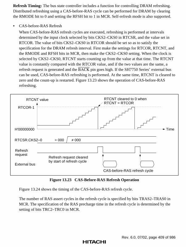
Rev. 6.0, 07/02, page 409 of 986
Refresh Timing: The bus state controller includes a function for controlling DRAM refreshing.Distributed refreshing using a CAS-before-RAS cycle can be performed for DRAM by clearingthe RMODE bit to 0 and setting the RFSH bit to 1 in MCR. Self-refresh mode is also supported.
• CAS-before-RAS Refresh
When CAS-before-RAS refresh cycles are executed, refreshing is performed at intervalsdetermined by the input clock selected by bits CKS2–CKS0 in RTCSR, and the value set inRTCOR. The value of bits CKS2–CKS0 in RTCOR should be set so as to satisfy thespecification for the DRAM refresh interval. First make the settings for RTCOR, RTCNT, andthe RMODE and RFSH bits in MCR, then make the CKS2–CKS0 setting. When the clock isselected by CKS2–CKS0, RTCNT starts counting up from the value at that time. The RTCNTvalue is constantly compared with the RTCOR value, and if the two values are the same, arefresh request is generated and the BACK pin goes high. If the SH7750 Series’ external buscan be used, CAS-before-RAS refreshing is performed. At the same time, RTCNT is cleared tozero and the count-up is restarted. Figure 13.23 shows the operation of CAS-before-RASrefreshing.
RTCNT value
RTCOR-1
H'00000000
RTCSR.CKS2–0
External bus
Refresh request cleared by start of refresh cycle
= 000 ≠ 000
RTCNT cleared to 0 when RTCNT = RTCOR
CAS-before-RAS refresh cycle
Time
Refresh request
Figure 13.23 CAS-Before-RAS Refresh Operation
Figure 13.24 shows the timing of the CAS-before-RAS refresh cycle.
The number of RAS assert cycles in the refresh cycle is specified by bits TRAS2–TRAS0 inMCR. The specification of the RAS precharge time in the refresh cycle is determined by thesetting of bits TRC2–TRC0 in MCR.

Rev. 6.0, 07/02, page 410 of 986
TRr2 TRr3 TRr4 TRr5 TrcTRr1 Trc Trc
CKIO
A25–A0
RD/
D63–D0
Figure 13.24 DRAM CAS-Before-RAS Refresh Cycle Timing (TRAS = 0, TRC = 1)
• Self-Refresh
The self-refreshing supported by the SH7750 Series is shown in figure 13.25.
After the self-refresh is cleared, the refresh controller immediately generates a refresh request.The RAS precharge time immediately after the end of the self-refreshing can be set by bitsTRC2–TRC0 in MCR.
DRAMs include low-power products (L versions) with a long refresh cycle time (for example,the HM51W4160AL L version has a refresh cycle of 1024 cycles/128 ms compared with 1024cycles/16 ms for the normal version). With these DRAMs, however, the same refresh cycle asfor the normal version is requested only in the case of refreshing immediately following self-refreshing. To ensure efficient DRAM refreshing, therefore, processing is needed to generatean overflow interrupt and restore the refresh cycle to the proper value, after the necessaryCAS-before-RAS refreshing has been performed following self-refreshing of an L-versionDRAM, using the OVF, OVIE, and LMTS bits in RTCSR and the refresh controller’s refreshcount register (RFCR). The necessary procedure is as follows.

Rev. 6.0, 07/02, page 411 of 986
1. Normally, set the refresh counter count cycle to the optimum value for the L version (e.g.1024 cycles/128 ms).
2. When a transition is made to self-refreshing:
a. Provide an interrupt handler to restore the refresh counter count value to the optimumvalue for the L version (e.g. 1024 cycles/128 ms) when a refresh counter overflowinterrupt is generated.
b. Re-set the refresh counter count cycle to the requested short cycle (e.g. 1024 cycles/16ms), set refresh controller overflow interruption, and clear the refresh controller’srefresh count register (RFCR) to 0.
c. Set self-refresh mode.
By using this procedure, the refreshing immediately following a self-refresh will be performedin a short cycle, and when adequate refreshing ends, an interrupt is generated and the settingcan be restored to the original refresh cycle.
CAS-before-RAS refreshing is performed in normal operation, in sleep mode, and in the caseof a manual reset.
Self-refreshing is performed in normal operation, in sleep mode, in standby mode, and in thecase of a manual reset.
When the bus has been released in response to a bus arbitration request, or when a transition ismade to standby mode, signals generally become high-impedance, but whether the RAS andCAS signals become high-impedance or continue to be output can be controlled by theHIZCNT bit in BCR1. This enables the DRAM to be kept in the self-refreshing state.
As the DRAM CAS signal is multiplexed with WEn for normal memory (SRAM, etc.), accessto memory that uses the WEn signals must be disabled during self-refreshing.
• Relationship between Refresh Requests and Bus Cycle Requests
If a refresh request is generated during execution of a bus cycle, execution of the refresh isdeferred until the bus cycle is completed. Refresh operations are deferred during multiple buscycles generated because the data bus width is smaller than the access size (for example, whenperforming longword access to 8-bit bus width memory) and during a 32-byte transfer such asa cache fill or write-back, and also between read and write cycles during execution of a TASinstruction, and between read and write cycles when DMAC dual address transfer is executed.If a refresh request occurs when the bus has been released by the bus arbiter, refresh executionis deferred until the bus is acquired. If a match between RTCNT and RTCOR occurs while arefresh is waiting to be executed, so that a new refresh request is generated, the previousrefresh request is eliminated. In order for refreshing to be performed normally, care must betaken to ensure that no bus cycle or bus mastership occurs that is longer than the refreshinterval. When a refresh request is generated, the BACK pin is negated (driven high).Therefore, normal refreshing can be performed by having the BACK pin monitored by a bus

Rev. 6.0, 07/02, page 412 of 986
master other than the SH7750 Series requesting the bus, or the bus arbiter, and returning thebus to the SH7750 Series.
TRr2 TRr3 TRr4 TRr5 TrcTRr1 Trc Trc
CKIO
A25–A0
RD/
D63–D0
Figure 13.25 DRAM Self-Refresh Cycle Timing
Power-On Sequence: Regarding use of DRAM after powering on, it is requested that a wait time(at least 100 µs or 200 µs) during which no access can be performed be provided, followed by atleast the prescribed number (usually 8) of dummy CAS-before-RAS refresh cycles. As the busstate controller does not perform any special operations for a power-on reset, the necessary power-on sequence must be carried out by the initialization program executed after a power-on reset.

Rev. 6.0, 07/02, page 413 of 986
13.3.5 Synchronous DRAM Interface
Connection of Synchronous DRAM: Since synchronous DRAM can be selected by the CSsignal, it can be connected to physical space areas 2 and 3 using RAS and other control signals incommon. If the memory type bits (DRAMTP2–0) in BCR1 are set to 010, area 2 is normalmemory space and area 3 is synchronous DRAM space; if set to 011, areas 2 and 3 are bothsynchronous DRAM space.
With the SH7750 Series, burst read/burst write mode is supported as the synchronous DRAMoperating mode. The data bus width is 32 or 64 bits, and the SZ size bits in MCR must be set to 00or 11. The burst enable bit (BE) in MCR is ignored, a 32-byte burst transfer is performed in acache fill/copy-back cycle, and in a write-through area write or a non-cacheable area read/write,32-byte data is read even in a single read in order to access synchronous DRAM with a burstread/write access. 32-byte data transfer is also performed in a single write, but DQMn is notasserted when unnecessary data is transferred. For details on the burst length, see section 13.2.10,Synchronous DRAM Module Register (SDMR), and Power-On Sequence in section 13.3.5,Synchronous DRAM Interface. For changing the burst length (a function only available in theSH7750R) for a 32-bit bus, see Notes on Changing the Burst Length (SH7750R Only) in section13.3.5, Synchronous DRAM Interface.
The control signals for connection of synchronous DRAM are RAS, CAS, RD/WR, CS2 or CS3,DQM0 to DQM7, and CKE. All the signals other than CS2 and CS3 are common to all areas, andsignals other than CKE are valid and latched only when CS2 or CS3 is asserted. SynchronousDRAM can therefore be connected in parallel to a number of areas. CKE is negated (driven low)when the frequency is changed, when the clock is unstable after the clock supply is stopped andrestarted, or when self-refreshing is performed, and is always asserted (high) at other times.
Commands for synchronous DRAM are specified by RAS, CAS, RD/WR, and specific addresssignals. The commands are NOP, auto-refresh (REF), self-refresh (SELF), precharge all banks(PALL), precharge specified bank (PRE), row address strobe bank active (ACTV), read (READ),read with precharge (READA), write (WRIT), write with precharge (WRITA), and mode registersetting (MRS).
Byte specification is performed by DQM0 to DQM7. A read/write is performed for the byte forwhich the corresponding DQM signal is low. When the bus width is 64 bits, in big-endian modeDQM7 specifies an access to address 8n, and DQM0 specifies an access to address 8n + 7. Inlittle-endian mode, DQM7 specifies an access to address 8n + 7, and DQM0 specifies an access toaddress 8n.
Figures 13.26 and 13.27 show examples of the connection of 16M × 16-bit synchronous DRAMs.

Rev. 6.0, 07/02, page 414 of 986
A12–A3CKIOCKE
RD/D63–D48
DQM7DQM6
SH7750 Series512k × 16-bit × 2-banksynchronous DRAM
A9–A0CLKCKE
I/O15–I/O0DQMUDQML
D47–D32DQM5DQM4
D31–D16DQM3DQM2
D15–D0DQM1DQM0
A9–A0CLKCKE
I/O15–I/O0DQMUDQML
A9–A0CLKCKE
I/O15–I/O0DQMUDQML
A9–A0CLKCKE
I/O15–I/O0DQMUDQML
Figure 13.26 Example of 64-Bit Data Width Synchronous DRAM Connection (Area 3)

Rev. 6.0, 07/02, page 415 of 986
A11–A2CKIOCKE
RD/D31–D16
DQM3DQM2
SH7750 Series512k × 16-bit × 2-banksynchronous DRAM
A9–A0CLKCKE
I/O15–I/O0DQMUDQML
D15–D0DQM1DQM0
A9–A0CLKCKE
I/O15–I/O0DQMUDQML
Figure 13.27 Example of 32-Bit Data Width Synchronous DRAM Connection (Area 3)
Address Multiplexing: Synchronous DRAM can be connected without external multiplexingcircuitry in accordance with the address multiplex specification bits AMXEXT and AMX2–AMX0 in MCR. Table 13.16 shows the relationship between the address multiplex specificationbits and the bits output at the address pins. See Appendix F, Synchronous DRAM AddressMultiplexing Tables.
Address pin output at A25–A18, A1, and A0 are undefined.
When A0, the LSB of the synchronous DRAM address, is connected to the SH7750 Series, with a32-bit bus width it makes a longword address specification. Connection should therefore be madein this order: connect pin A0 of the synchronous DRAM to pin A2 of the SH7750, then connectpin A1 to pin A3.
With a 64-bit bus width, the LSB makes a quadword address specification. Connection shouldtherefore be made in this order: connect pin A0 of the synchronous DRAM to pin A3 of theSH7750, then connect pin A1 to pin A4.

Rev. 6.0, 07/02, page 416 of 986
Table 13.16 Example of Correspondence between SH7750 Series and Synchronous DRAMAddress Pins (64-Bit Bus Width, AMX2–AMX0 = 011, AMXEXT = 0)
SH7750 Series Address Pin Synchronous DRAM Address Pin
RAS Cycle CAS Cycle Function
A14 A22 A22 A11 BANK select bank address
A13 A21 H/L A10 Address precharge setting
A12 A20 0 A9
A11 A19 0 A8
A10 A18 A10 A7
A9 A17 A9 A6
A8 A16 A8 A5
A7 A15 A7 A4
A6 A14 A6 A3
A5 A13 A5 A2
A4 A12 A4 A1
A3 A11 A3 A0
A2 — A2 Not used
A1 — A1 Not used
A0 — A0 Not used
Burst Read: The timing chart for a burst read is shown in figure 13.28. In the following exampleit is assumed that four 512k × 16-bit × 2-bank synchronous DRAMs are connected, and a 64-bitdata width is used. The burst length is 4. Following the Tr cycle in which ACTV command outputis performed, a READA command is issued in the Tc1 cycle, and the read data is accepted on therising edge of the external command clock (CKIO) from cycle Td1 to cycle Td4. The Tpc cycle isused to wait for completion of auto-precharge based on the READA command inside thesynchronous DRAM; no new access command can be issued to the same bank during this cycle. Inthe SH7750 Series, the number of Tpc cycles is determined by the specification of bits TPC2–TPC0 in MCR, and commands are not issued for synchronous DRAM during this interval.
The example in figure 13.28 shows the basic cycle. To connect slower synchronous DRAM, thecycle can be extended by setting WCR2 and MCR bits. The number of cycles from the ACTVcommand output cycle, Tr, to the READA command output cycle, Tc1, can be specified by bitsRCD1 and RCD0 in MCR, with a value of 0 to 3 specifying 2 to 4 cycles, respectively. In the caseof 2 or more cycles, a Trw cycle, in which an NOP command is issued for the synchronousDRAM, is inserted between the Tr cycle and the Tc cycle. The number of cycles from READAcommand output cycle Tc1 to the first read data latch cycle, Td1, can be specified as 1 to 5 cyclesindependently for areas 2 and 3 by means of bits A2W2–A2W0 and A3W2–A3W0 in WCR2.This number of cycles corresponds to the number of synchronous DRAM CAS latency cycles.

Rev. 6.0, 07/02, page 417 of 986
Tr Trw Tc1 Tc2 Tc3 Tc4/Td1 Td3Td2 Td4
CKIO
Bank
Precharge-sel
Address
RD/
D63–D0(read)
DQMn
DACKn(SA: IO ← memory)
CKE
H/L
c0
d0 d1 d2 d3
Row
Row
Row
Note: For DACKn, an example is shown where CHCRn.AL (access level) = 0 for the DMAC.
Figure 13.28 Basic Timing for Synchronous DRAM Burst Read
In a synchronous DRAM cycle, the BS signal is asserted for one cycle at the start of the datatransfer cycle corresponding to the READ or READA command. The order of access is asfollows: in a fill operation in the event of a cache miss, 64-bit boundary data including the misseddata is read first, then 16-byte boundary data including the missed data is read in wraparoundmode. The remaining 16 bytes of the 32-byte boundary data are read by the READA commandissued next.

Rev. 6.0, 07/02, page 418 of 986
Single Read: With the SH7750 Series, as synchronous DRAM is set to burst read/burst writemode, read data output continues after the required data has been read. To prevent data collisions,after the required data is read in Td1, empty read cycles Td2 to Td4 are performed, and theSH7750 Series waits for the end of the synchronous DRAM operation. The BS signal is assertedonly in Td1.
When the data width is 64 bits, there are 4 burst transfers in a read. In cache-through and otherDMA read cycles, of cycles Td1 to Td4, BS is asserted and data latched only in the Td1 cycle.
Since such empty cycles increase the memory access time, and tend to reduce program executionspeed and DMA transfer speed, it is important both to avoid unnecessary cache-through areaaccesses, and to use a data structure that will allow data to be placed at a 32-byte boundary, and tobe transferred in 32-byte units, when carrying out DMA transfer with synchronous DRAMspecified as the source.
Tr Tc1 Tc2
c1
Tc3 Tc4/Td1 Td2 Td4Trw
H/L
c1
Td3 Tpc TpcTpc
CKIO
Bank
Precharge-sel
Address
DQMn
RD/
D63–D0(read)
CKE
DACKn(SA: IO ← memory)
Row
Row
Row
Note: For DACKn, an example is shown where CHCRn.AL (access level) = 0 for the DMAC.
Figure 13.29 Basic Timing for Synchronous DRAM Single Read

Rev. 6.0, 07/02, page 419 of 986
Burst Write: The timing chart for a burst write is shown in figure 13.30. In the SH7750 Series, aburst write occurs only in the event of cache copy-back or a 32-byte transfer by the DMAC. In aburst write operation, the WRITA command is issued in the Tc1 cycle following the Tr cycle inwhich the ACTV command is output. In the write cycle, the write data is output at the same timeas the write command. In the case of the write with auto-precharge command, precharging of therelevant bank is performed in the synchronous DRAM after completion of the write command,and therefore no command can be issued for the same bank until precharging is completed.Consequently, in addition to the precharge wait cycle, Tpc, used in a read access, cycle Trwl isalso added as a wait interval until precharging is started following the write command. Issuance ofa new command for synchronous DRAM is postponed during this interval. The number of Trwlcycles can be specified by bits TRWL2–TRWL0 in MCR. 32-byte boundary data is written inwraparound mode. DACK is asserted two cycles before the data write cycle.
Tr Tc1 Tc2 Tc3 Tc4 Trw1 TpcTrw
H/L
c1
Trw1
CKIO
Bank
Precharge-sel
Address
DQMn
RD/
D63–D0(read)
CKE
DACKn(SA: IO → memory)
c1 c2 c3 c4
Row
Row
Row
Note: For DACKn, an example is shown where CHCRn.AL (access level) = 0 for the DMAC.
Figure 13.30 Basic Timing for Synchronous DRAM Burst Write

Rev. 6.0, 07/02, page 420 of 986
Single Write: The basic timing chart for write access is shown in figure 13.31. In a single writeoperation, following the Tr cycle in which ACTV command output is performed, a WRITAcommand that performs auto-precharge is issued in the Tc1 cycle. In the write cycle, the write datais output at the same time as the write command. In the case of a write with auto-precharge,precharging of the relevant bank is performed in the synchronous DRAM after completion of thewrite command, and therefore no command can be issued for synchronous DRAM untilprecharging is completed. Consequently, in addition to the precharge wait cycle, Tpc, used in aread access, cycle Trwl is also added as a wait interval until precharging is started following thewrite command. Issuance of a new command for synchronous DRAM is postponed during thisinterval. The number of Trwl cycles can be specified by bits TRWL2–TRWL0 in MCR. DACK isasserted two cycles before the data write cycle.
As the SH7750 Series supports burst read/burst write operations for synchronous DRAM, thereare empty cycles in a single write operation.

Rev. 6.0, 07/02, page 421 of 986
Tr Tc1 Tc2 Tc3 Tc4 Trw1 TpcTrw
H/L
c1
Trw1
CKIO
Bank
Precharge-sel
Address
DQMn
RD/
D63–D0(read)
CKE
DACKn(SA: IO → memory)
c1
Row
Row
Row
Note: For DACKn, an example is shown where CHCRn.AL (access level) = 0 for the DMAC.
Figure 13.31 Basic Timing for Synchronous DRAM Single Write

Rev. 6.0, 07/02, page 422 of 986
RAS Down Mode: The synchronous DRAM bank function is used to support high-speed accessesto the same row address. When the RASD bit in MCR is 1, read/write command accesses areperformed using commands without auto-precharge (READ, WRIT). In this case, precharging isnot performed when the access ends. When accessing the same row address in the same bank, it ispossible to issue the READ or WRIT command immediately, without issuing an ACTV command,in the same way as in the DRAM RAS down state. As synchronous DRAM is internally dividedinto two or four banks, it is possible to activate one row address in each bank. If the next access isto a different row address, a PRE command is first issued to precharge the relevant bank, thenwhen precharging is completed, the access is performed by issuing an ACTV command followedby a READ or WRIT command. If this is followed by an access to a different row address, theaccess time will be longer because of the precharging performed after the access request is issued.
In a write, when auto-precharge is performed, a command cannot be issued for a period of Trwl +Tpc cycles after issuance of the WRIT command. When RAS down mode is used, READ orWRIT commands can be issued successively if the row address is the same. The number of cyclescan thus be reduced by Trwl + Tpc cycles for each write. The number of cycles between issuanceof the precharge command and the row address strobe command is determined by bits TPC2–TPC0 in MCR.
There is a limit on tRAS, the time for placing each bank in the active state. If there is no guaranteethat there will not be a cache hit and another row address will be accessed within the period inwhich this value is maintained by program execution, it is necessary to set auto-refresh and set therefresh cycle to no more than the maximum value of tRAS. In this way, it is possible to observe therestrictions on the maximum active state time for each bank. If auto-refresh is not used, measuresmust be taken in the program to ensure that the banks do not remain active for longer than theprescribed time.
A burst read cycle without auto-precharge is shown in figure 13.32, a burst read cycle for the samerow address in figure 13.33, and a burst read cycle for different row addresses in figure 13.34.Similarly, a burst write cycle without auto-precharge is shown in figure 13.35, a burst write cyclefor the same row address in figure 13.36, and a burst write cycle for different row addresses infigure 13.37.
When synchronous DRAM is read, there is a 2-cycle latency for the DMQn signal that performsthe byte specification. As a result, when the READ command is issued in figure 13.32, if the Tccycle is executed immediately, the DMQn signal specification for Td1 cycle data output cannot becarried out. Therefore, the CAS latency should not be set to 1.
When RAS down mode is set, if only accesses to the respective banks in area 3 are considered, aslong as accesses to the same row address continue, the operation starts with the cycle in figure13.32 or 13.35, followed by repetition of the cycle in figure 13.33 or 13.36. An access to adifferent area during this time has no effect. If there is an access to a different row address in thebank active state, after this is detected the bus cycle in figure 13.34 or 13.37 is executed instead of

Rev. 6.0, 07/02, page 423 of 986
that in figure 13.33 or 13.36. In RAS down mode, too, a PALL command is issued before a refreshcycle or before bus release due to bus arbitration.
c2 c3 c4
Tr Tc1 Tc2
c1
Tc3 Tc4/Td1 Td2 Td4Trw
H/L
c1
Td3
CKIO
Bank
Precharge-sel
Address
DQMn
RD/
D63–D0(read)
CKE
DACKn(SA: IO ← memory)
Row
Row
Row
Note: For DACKn, an example is shown where CHCRn.AL (access level) = 0 for the DMAC.
Figure 13.32 Burst Read Timing

Rev. 6.0, 07/02, page 424 of 986
c2 c3 c4
Tc1 Tc3 Tc4/Td1
c1
Td2 Td3 Td4Tc2
H/L
c1
CKIO
Bank
Precharge-sel
Address
DQMn
RD/
D63–D0(read)
CKE
DACKn(SA: IO ← memory)
Note: For DACKn, an example is shown where CHCRn.AL (access level) = 0 for the DMAC.
Figure 13.33 Burst Read Timing (RAS Down, Same Row Address)

Rev. 6.0, 07/02, page 425 of 986
Tpr Tr Trw
c1 c2 c3 c4
Tc1 Tc2 Tc3 Td2Tpc
H/L
c1
Tc4/Td1 Td3 Td4
CKIO
Bank
Precharge-sel Row
Row
Row
Address
DQMn
RD/
D63–D0(read)
CKE
DACKn(SA: IO ← memory)
Note: For DACKn, an example is shown where CHCRn.AL (access level) = 0 for the DMAC.
Figure 13.34 Burst Read Timing (RAS Down, Different Row Addresses)

Rev. 6.0, 07/02, page 426 of 986
Tr Tc1 Tc2 Tc3 Tc4 Trw1Trw
H/L
c1
Trw1
CKIO
Bank
Precharge-sel
Address
DQMn
RD/
D63–D0(read)
CKE
c1 c2 c3 c4
Row
Row
Row
DACKn(SA: IO → memory)
Note: For DACKn, an example is shown where CHCRn.AL (access level) = 0 for the DMAC.
Figure 13.35 Burst Write Timing

Rev. 6.0, 07/02, page 427 of 986
Tnop Tc2 Tc3 Tc4 Trw1 Trw1Tc1
H/L
c1
Tncp
CKIO
Bank
Precharge-sel
Address
DQMn
RD/
D63–D0(read)
CKE
c1 c2 c3 c4
Row
DACKn(SA: IO → memory)
Single-address DMA
Normal write
Note: In the case of SA-DMA only, the (Tnop) cycle is inserted, and the DACKn signal is output as shown by the solid line. In a normal write, the (Tnop) cycle is omitted and the DACKn signal is output as shown by the dotted line. DACKn shows an example where DMAC, CHCRn, and AL (acknowledge level) are 0.
Figure 13.36 Burst Write Timing (Same Row Address)

Rev. 6.0, 07/02, page 428 of 986
Tpr Tr Trw Tc1 Tc2 Tc3Tpc
H/L
c1
Tc4 Trw1 Trw1 Trw1
CKIO
Bank
Precharge-sel
Address
DQMn
RD/
D63–D0(read)
CKE
DACKn(SA: IO → memory)
c1 c2 c3 c4
Row
Row
Row
Note: For DACKn, an example is shown where CHCRn.AL (access level) = 0 for the DMAC.
Figure 13.37 Burst Write Timing (Different Row Addresses)
Pipelined Access: When the RASD bit is set to 1 in MCR, pipelined access is performed betweenan access by the CPU and an access by the DMAC, or in the case of consecutive accesses by theDMAC, to provide faster access to synchronous DRAM. As synchronous DRAM is internallydivided into two or four banks, after a READ or WRIT command is issued for one bank it ispossible to issue a PRE, ACTV, or other command during the CAS latency cycle or data latchcycle, or during the data write cycle, and so shorten the access cycle.
When a read access is followed by another read access to the same row address, after a READcommand has been issued, another READ command is issued before the end of the data latchcycle, so that there is read data on the data bus continuously. When an access is made to another

Rev. 6.0, 07/02, page 429 of 986
row address and the bank is different, the PRE command or ACTV command can be issued duringthe CAS latency cycle or data latch cycle. If there are consecutive access requests for different rowaddresses in the same bank, the PRE command cannot be issued until the last-but-one data latchcycle. If a read access is followed by a write access, it may be possible to issue a PRE or ACTcommand, depending on the bank and row address, but since the write data is output at the sametime as the WRIT command, the PRE, ACTV, and WRIT commands are issued in such a way thatone or two empty cycles occur automatically on the data bus. Similarly, with a read accessfollowing a write access, or a write access following a write access, the PRE, ACTV, READ, orWRIT command is issued during the data write cycle for the preceding access; however, in thecase of different row addresses in the same bank, a PRE command cannot be issued, and so in thiscase the PRE command is issued following the number of Trwl cycles specified by the TRWL bitsin MCR, after the end of the last data write cycle.
Figure 13.38 shows a burst read cycle for a different bank and row address following a precedingburst read cycle.
Pipelined access is enabled only for consecutive access to area 3, and will be discontinued in theevent of an access to another area. Pipelined access is also discontinued in the event of a refreshcycle, or bus release due to bus arbitration. The cases in which pipelined access is available areshown in table 13.17. In this table, “DMAC dual” indicates transfer in DMAC dual address mode,and “DMAC single”, transfer in DMAC single address mode.

Rev. 6.0, 07/02, page 430 of 986
Tc1_A Tc1_B
H/L
c_B
CKIO
Bank
Precharge-sel
Address
DQMn
RD/
D63–D0(read)
CKE
a1 a2 a3 a4 b1 b2
c_A
H/L
Note: For DACKn, an example is shown where CHCRn.AL (access level) = 0 for the DMAC.
Figure 13.38 Burst Read Cycle for Different Bank and Row Address Following PrecedingBurst Read Cycle
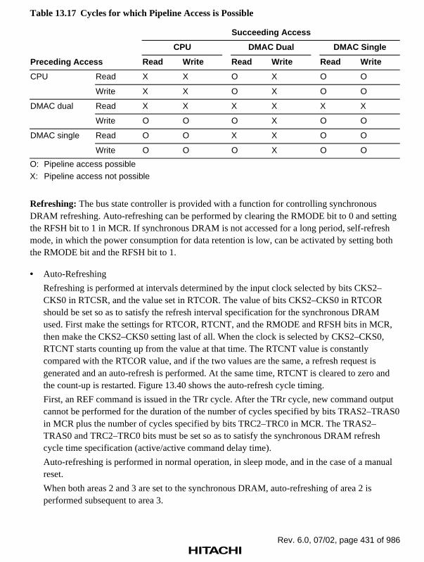
Rev. 6.0, 07/02, page 431 of 986
Table 13.17 Cycles for which Pipeline Access is Possible
Succeeding Access
CPU DMAC Dual DMAC Single
Preceding Access Read Write Read Write Read Write
CPU Read X X O X O O
Write X X O X O O
DMAC dual Read X X X X X X
Write O O O X O O
DMAC single Read O O X X O O
Write O O O X O O
O: Pipeline access possibleX: Pipeline access not possible
Refreshing: The bus state controller is provided with a function for controlling synchronousDRAM refreshing. Auto-refreshing can be performed by clearing the RMODE bit to 0 and settingthe RFSH bit to 1 in MCR. If synchronous DRAM is not accessed for a long period, self-refreshmode, in which the power consumption for data retention is low, can be activated by setting boththe RMODE bit and the RFSH bit to 1.
• Auto-Refreshing
Refreshing is performed at intervals determined by the input clock selected by bits CKS2–CKS0 in RTCSR, and the value set in RTCOR. The value of bits CKS2–CKS0 in RTCORshould be set so as to satisfy the refresh interval specification for the synchronous DRAMused. First make the settings for RTCOR, RTCNT, and the RMODE and RFSH bits in MCR,then make the CKS2–CKS0 setting last of all. When the clock is selected by CKS2–CKS0,RTCNT starts counting up from the value at that time. The RTCNT value is constantlycompared with the RTCOR value, and if the two values are the same, a refresh request isgenerated and an auto-refresh is performed. At the same time, RTCNT is cleared to zero andthe count-up is restarted. Figure 13.40 shows the auto-refresh cycle timing.
First, an REF command is issued in the TRr cycle. After the TRr cycle, new command outputcannot be performed for the duration of the number of cycles specified by bits TRAS2–TRAS0in MCR plus the number of cycles specified by bits TRC2–TRC0 in MCR. The TRAS2–TRAS0 and TRC2–TRC0 bits must be set so as to satisfy the synchronous DRAM refreshcycle time specification (active/active command delay time).
Auto-refreshing is performed in normal operation, in sleep mode, and in the case of a manualreset.
When both areas 2 and 3 are set to the synchronous DRAM, auto-refreshing of area 2 isperformed subsequent to area 3.

Rev. 6.0, 07/02, page 432 of 986
RTCNT value
RTCOR-1
H'00000000
RTCSR.CKS2–0
External bus
Refresh request cleared by start of refresh cycle
= 000 ≠ 000
RTCNT cleared to 0 when RTCNT = RTCOR
Auto-refresh cycle
Time
Refresh request
Figure 13.39 Auto-Refresh Operation
TRr2 TRr3 TRr4 TRr5 TrcTRr1 TrcTRrw Trc
CKIO
RD/
DQMn
CKE
D63–D0
Figure 13.40 Synchronous DRAM Auto-Refresh Timing

Rev. 6.0, 07/02, page 433 of 986
• Self-Refreshing
Self-refresh mode is a kind of standby mode in which the refresh timing and refresh addressesare generated within the synchronous DRAM. Self-refreshing is activated by setting both theRMODE bit and the RFSH bit to 1. The self-refresh state is maintained while the CKE signalis low. Synchronous DRAM cannot be accessed while in the self-refresh state. Self-refreshmode is cleared by clearing the RMODE bit to 0. After self-refresh mode has been cleared,command issuance is disabled for the number of cycles specified by bits TRC2–TRC0 inMCR. Self-refresh timing is shown in figure 13.41. Settings must be made so that self-refreshclearing and data retention are performed correctly, and auto-refreshing is performed at thecorrect intervals. When self-refreshing is activated from the state in which auto-refreshing isset, or when exiting standby mode other than through a power-on reset, auto-refreshing isrestarted if RFSH is set to 1 and RMODE is cleared to 0 when self-refresh mode is cleared. Ifthe transition from clearing of self-refresh mode to the start of auto-refreshing takes time, thistime should be taken into consideration when setting the initial value of RTCNT. Making theRTCNT value 1 less than the RTCOR value will enable refreshing to be started immediately.
After self-refreshing has been set, the self-refresh state continues even if the chip standby stateis entered using the SH7750 Series’ standby function, and is maintained even after recoveryfrom standby mode other than through a power-on reset.
In the case of a power-on reset, the bus state controller’s registers are initialized, and thereforethe self-refresh state is cleared.
Self-refreshing is performed in normal operation, in sleep mode, in standby mode, and in thecase of a manual reset.

Rev. 6.0, 07/02, page 434 of 986
TRs2 TRs3 TRs4 TRs5 TrcTRs1 Trc Trc
CKIO
RD/
DQMn
CKE
D63–D0
Figure 13.41 Synchronous DRAM Self-Refresh Timing
• Relationship between Refresh Requests and Bus Cycle Requests
If a refresh request is generated during execution of a bus cycle, execution of the refresh isdeferred until the bus cycle is completed. Refresh operations are deferred during multiple buscycles generated because the data bus width is smaller than the access size (for example, whenperforming longword access to 8-bit bus width memory) and during a 32-byte transfer such asa cache fill or write-back, and also between read and write cycles during execution of a TASinstruction, and between read and write cycles when DMAC dual address transfer is executed.If a refresh request occurs when the bus has been released by the bus arbiter, refresh executionis deferred until the bus is acquired. If a match between RTCNT and RTCOR occurs while arefresh is waiting to be executed, so that a new refresh request is generated, the previousrefresh request is eliminated. In order for refreshing to be performed normally, care must betaken to ensure that no bus cycle or bus mastership occurs that is longer than the refreshinterval. When a refresh request is generated, the BACK pin is negated (driven high).Therefore, normal refreshing can be performed by having the BACK pin monitored by a busmaster other than the SH7750 Series requesting the bus, or the bus arbiter, and returning thebus to the SH7750 Series.

Rev. 6.0, 07/02, page 435 of 986
Power-On Sequence: In order to use synchronous DRAM, mode setting must first be performedafter powering on. To perform synchronous DRAM initialization correctly, the bus state controllerregisters must first be set, followed by a write to the synchronous DRAM mode register. Insynchronous DRAM mode register setting, the address signal value at that time is latched by acombination of the RAS, CAS, and RD/WR signals. If the value to be set is X, the bus statecontroller provides for value X to be written to the synchronous DRAM mode register byperforming a write to address H'FF900000 + X for area 2 synchronous DRAM, and to addressH'FF940000 + X for area 3 synchronous DRAM. In this operation the data is ignored, but themode write is performed as a byte-size access. To set burst read/write, CAS latency 1 to 3, wraptype = sequential, and burst length 4* or 8, supported by the SH7750, arbitrary data is written bybyte-size access to the following addresses.
Bus Width Burst Length CAS Latency Area 2 Area 3
32 4* 1
2
3
H'FF900048
H'FF900088
H'FF9000C8
H'FF940048
H'FF940088
H'FF9400C8
32 8 1 H'FF90004C H'FF94004C
2 H'FF90008C H'FF94008C
3 H'FF9000CC H'FF9400CC
64 4 1 H'FF900090 H'FF940090
2 H'FF900110 H'FF940110
3 H'FF900190 H'FF940190
Note: * SH7750R only.
The value set in MCR.MRSET is used to select whether a precharge all banks command or amode register setting command is issued. The timing for the precharge all banks command isshown in figure 13.42 (1), and the timing for the mode register setting command in figure13.42 (2).
Before mode register, a 200 µs idle time (depending on the memory manufacturer) must beguaranteed after the power required for the synchronous DRAM is turned on. If the reset signalpulse width is greater than this idle time, there is no problem in making the precharge all bankssetting immediately.
First, a precharge all banks (PALL) command is issued in the TRp1 cycle by performing a write toaddress H'FF900000 + X or H'FF940000 + X while MCR.MRSET = 0. Next, the number ofdummy auto-refresh cycles specified by the manufacturer (usually 8) or more must be executed.This is achieved automatically while various kinds of initialization are being performed after auto-refresh setting, but a way of carrying this out more dependably is to change the RTCOR registervalue to set a short refresh request generation interval just while these dummy cycles are beingexecuted. With simple read or write access, the address counter in the synchronous DRAM usedfor auto-refreshing is not initialized, and so the cycle must always be an auto-refresh cycle. After

Rev. 6.0, 07/02, page 436 of 986
auto-refreshing has been executed at least the prescribed number of times, a mode register settingcommand is issued in the TMw1 cycle by setting MCR.MRSET to 1 and performing a write toaddress H'FF900000 + X or H'FF940000 + X.
Synchronous DRAM mode register setting should be executed once only after power-on (reset)and before synchronous DRAM access, and no subsequent changes should be made.
CKIO
Bank
Precharge-sel
Address
RD/
D31–D0
CKE
TRp1 TRp2 TRp3 TRp4 TMw1 TMw2 TMw3 TMw4
(High)
TMw5
Figure 13.42 (1) Synchronous DRAM Mode Write Timing (PALL)

Rev. 6.0, 07/02, page 437 of 986
CKIO
Bank
Precharge-sel
Address
RD/
D31–D0
CKE
TRp1 TRp2 TRp3 TRp4 TMw1 TMw2 TMw3 TMw4
(High)
TMw5
Figure 13.42 (2) Synchronous DRAM Mode Write Timing (Mode Register Set)

Rev. 6.0, 07/02, page 438 of 986
Notes on Changing the Burst Length (SH7750R Only): In the SH7750R, when synchronousDRAM is connected with a 32-bit memory bus, the burst length can be selected as either 4 or 8 bythe setting of the SDBL bit of the BCR3 register. For more details, see the description of theBCR3 register.
• Burst Read
Figure 13.43 is the timing chart of a burst-read operation with a burst length of 4. Followingthe Tr cycle, during which an ACTV command is output, a READ command is issued duringcycle Tc1, and a READA command is issued four cycles later. During the Td1 to Td8 cycles,read data are accepted on the rising edges of the external command clock (CKIO). Tpc is thecycle used to wait for the auto-precharging, which is triggered by the READA command, to becompleted in the synchronous DRAM. During this cycle, a new command for accessing thesame bank cannot be issued. In this LSI, the number of Tpc cycles is determined by the settingof the TPC2 to TPC0 bits of MCR, and no command that operates on the synchronous DRAMmay be issued during these cycles.
Tr Trw Tc1 Tc2 Tc3 Tc4/Td1 Td3Td2 Td4
CKIO
Bank
Precharge-sel
Address
RD/
D31–D0 (read)
DQMn
CKE
H/L
c5
Td5 Td6 Td8Td7 Tpc
H/L
c1
c1 c2 c3 c4 c7 c8c5 c6
DACKn(SA: IO ← memory)
Row
Row
Row
Note: For DACKn, an example is shown where CHCRn.AL (access level) = 0 for the DMAC.
Figure 13.43 Basic Timing of Synchronous DRAM Burst Read (Burst Length = 4)

Rev. 6.0, 07/02, page 439 of 986
In a synchronous DRAM cycle, the BS signal is asserted for one cycle at the beginning of eachdata transfer cycle that is in response to a READ or READA command. Data are accessed inthe following sequence: in the fill operation for a cache miss, the data between 64-bitboundaries that include the missing data are first read by the initial READ command; afterthat, the data between 16-bit boundaries data that include the missing data are read in awraparound way. The subsequently issued READA command reads the 16 bytes of data,which is the remainder of the data between 32-byte boundaries, from the start of the 16-byteboundary.
• Burst Write
Figure 13.44 is the timing chart for a burst-write operation with a burst length of 4. In this LSI,a burst write takes place when a 32-byte data transfer has occurred. In a burst-write operation,subsequent to the Tr cycle, in which ACTV command output takes place, a WRIT command isissued during the Tc1 cycle, and a WRITA command is issued four cycles later. During thewrite cycle, write data is output together with the write command. With a write command thatincludes an auto precharge, the precharge is performed on the relevant bank of thesynchronous DRAM on completion of the write command so no new command that accessesthe same bank can be issued until precharging is completed. For this reason, Trwl cycles,which are a period of waiting for precharging to start after the write command, are added. Thisis additional to the precharge-waiting cycle used in read access. These cycles delay the issuingof new commands to the synchronous DRAM. The setting of the TRWL2 to TRWL0 bits ofMCR selects the number of Trwl cycles. The data between 16-byte boundaries is firstaccessed, and the data between 32-byte boundaries are then written in a wraparound way.
DACK is asserted for two cycles before the data-write cycle.

Rev. 6.0, 07/02, page 440 of 986
Tr Tc1 Tc2 Tc3 Tc4 Tc5 Tc7Trw
c1
Tc6
DACKn(SA: IO → memory)
c1 c2 c3 c4 c5 c6 c7 c8
Row
Row
Tc8 Trw1 TpcTrw1
H/L H/L
c5
Row
CKIO
Bank
Precharge-sel
Address
DQMn
RD/
D31–D0 (read)
CKE
Note: For DACKn, an example is shown where CHCRn.AL (access level) = 0 for the DMAC.
Figure 13.44 Basic Timing of a Burst Write to Synchronous DRAM
Connecting a 128-Mbit/256-Mbit Synchronous DRAM with 64-bit Bus Width (SH7750ROnly): It is possible to connect 128-Mbit or 256-Mbit synchronous DRAMs with 64-bit bus widthto the SH7750R. RAS down mode is also available using a 128 Mbytes of external memory spacein area 2 or 3. Either eight 128-Mbit (4 M × 8 bit × 4 bank) DRAMs or four 256-Mbit (4 M × 8 bit× 4 bank) DRAMs can be connected. Figure 13.45 shows an example in which four 256-MbitDRAMs are connected.
Notes on Usage:
• BCR1.DRAMTP2−DRAMTP0 = 011: Sets areas 2 and 3 as synchronous-DRAM-interfacespaces.
• MCR.SZ = 00: Sets the bus width of the synchronous DRAM to 64 bits.
• MCR.AMX = 6: Selects the 128-Mbit or 256-Mbit address-multiplex setting for thesynchronous DRAM.
• In the auto-refresh operation, the REF command is issued twice in response to a single refreshrequest. Set RTCOR and bits CKS2−CKS0 so as to satisfy the refresh-interval rating of thesynchronous DRAM which you are using.
• When setting the mode register of the synchronous DRAM, set the address for area 2 first.
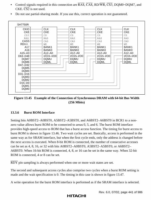
Rev. 6.0, 07/02, page 441 of 986
• Control signals required in this connection are RAS, CAS, RD/WR, CS3, DQM0−DQM7, andCKE. CS2 is not used.
• Do not use partial-sharing mode. If you use this, correct operation is not guaranteed.
CKIOCKECS3RAS
CASSRD/WR
A17A16
A15–A3D63–D48
DQM7DQM6
D47–D32DQM5DQM4
D31–D16DQM3DQM2
D15–D0DQM1DQM0
SH7750R
CLKCKECSRASCASWEBANK1BANK0A12–A0I/O15–I/O0DQMUDQML
CLKCKECSRASCASWEBANK1BANK0A12–A0I/O15–I/O0DQMUDQML
CLKCKECSRASCASWEBANK1BANK0A12–A0I/O15–I/O0DQMUDQML
CLKCKECSRASCASWEBANK1BANK0A12–A0I/O15–I/O0DQMUDQML
Figure 13.45 Example of the Connection of Synchronous DRAM with 64-bit Bus Width(256 Mbits)
13.3.6 Burst ROM Interface
Setting bits A0BST2–A0BST0, A5BST2–A5BST0, and A6BST2–A6BST0 in BCR1 to a non-zero value allows burst ROM to be connected to areas 0, 5, and 6. The burst ROM interfaceprovides high-speed access to ROM that has a burst access function. The timing for burst access toburst ROM is shown in figure 13.46. Two wait cycles are set. Basically, access is performed in thesame way as for SRAM interface, but when the first cycle ends, only the address is changed beforethe next access is executed. When 8-bit ROM is connected, the number of consecutive accessescan be set as 4, 8, 16, or 32 with bits A0BST2–A0BST0, A5BST2–A5BST0, or A6BST2–A6BST0. When 16-bit ROM is connected, 4, 8, or 16 can be set in the same way. When 32-bitROM is connected, 4 or 8 can be set.
RDY pin sampling is always performed when one or more wait states are set.
The second and subsequent access cycles also comprise two cycles when a burst ROM setting ismade and the wait specification is 0. The timing in this case is shown in figure 13.47.
A write operation for the burst ROM interface is performed as if the SRAM interface is selected.

Rev. 6.0, 07/02, page 442 of 986
In 32-byte transfer, a total of 32 bytes are transferred consecutively according to the set bus width.The first access is performed on the data for which there was an access request, and the remainingaccesses are performed on the data at the 32-byte boundary. The bus is not released during thisperiod.
Figure 13.48 shows the timing when a burst ROM setting is made, and setup/hold is specified inWCR3.
T1 TB1 TB2 TB1 TB2 TB1TB2 T2
CKIO
A25–A5
A4–A0
RD/
D63–D0(read)
DACKn(SA: IO ← memory)
Notes: 1. For a write cycle, a basic bus cycle (write cycle) is performed.2. For DACKn, an example is shown where CHCRn.AL (access level) = 0 for the DMAC.
Figure 13.46 Burst ROM Basic Access Timing

Rev. 6.0, 07/02, page 443 of 986
T1 Tw TB2 TB1 Tw TB2 TwTw TB1 TB2 Tw T2TB1
CKIO
A25–A5
A4–A0
RD/
D63–D0(read)
DACKn(SA: IO ← memory)
Notes: 1. For a write cycle, a basic bus cycle (write cycle) is performed.2. For DACKn, an example is shown where CHCRn.AL (access level) = 0 for the DMAC.
Figure 13.47 Burst ROM Wait Access Timing

Rev. 6.0, 07/02, page 444 of 986
CKIO
A25–A5
A4–A0
RD/
D63–D0(read)
DACKn(SA: IO ← memory)
TS1 TB2 TH1 TS1 TB1 TB2 TS1T1 TH1 TB1 TH1 TS1 TB1 T2 TH1TB2
Note: For DACKn, an example is shown where CHCRn.AL (access level) = 0 for the DMAC.
Figure 13.48 Burst ROM Wait Access Timing
13.3.7 PCMCIA Interface
In the SH7750 Series, setting the A56PCM bit in BCR1 to 1 makes the bus interface for externalmemory space areas 5 and 6 an IC memory card interface or I/O card interface as stipulated inJEIDA specification version 4.2 (PCMCIA2.1).
Figure 13.49 shows an example of PCMCIA card connection to the SH7750 Series. To enableactive insertion of the PCMCIA cards (i.e. insertion or removal while system power is beingsupplied), a 3-state buffer must be connected between the SH7750 Series’ bus interface and thePCMCIA cards.
As operation in big-endian mode is not explicitly stipulated in the JEIDA/PCMCIA specifications,the SH7750 Series supports only a little-endian mode PCMCIA interface.
In the SH7750, the PCMCIA interface area can only be accessed when the MMU is used. ThePCMCIA interface memory space can be set in page units and there is a choice of 8-bit commonmemory, 16-bit common memory, 8-bit attribute memory, 16-bit attribute memory, 8-bit I/Ospace, 16-bit I/O space, or dynamic bus sizing, according to the accessed SA2 to SA0 bits.
The setting for wait cycles during a bus access can also be made in MMU page units. When theTC bit to be accessed is cleared to 0, bits A5W2 to A5W0 in wait control register 2 (WCR2), andbits A5PCW1 and A5PCW0, A5TED2 to A5TED0, and A5TEH2 to A5TEH0 in the PCMCIA

Rev. 6.0, 07/02, page 445 of 986
control register (PCR), are selected. When the TC bit to be accessed is set to 1, bits A6W2 toA6W0 in wait control register 2 (WCR2), and bits A6PCW1 and A6PCW0, A6TED2 to A6TED0,and A6TEH2 to A6TEH0 in the PCMCIA control register (PCR), are selected. For the method ofsetting bits SA2 to SA0 and bit TC for the page to be accessed, see section 3, MemoryManagement Unit (MMU).
In the SH7750S and SH7750R, the PCMCIA interface can be accessed even when the MMU isnot used. When the MMU is off (MMUCR.AT=0), access is always performed by means of bitsSA2 to SA0 and bit TC in the page table entry assistance register (PTEA). When the MMU is on(MMUCR.AT=1), the situation is the same as for the SH7750.
In the SH7750 Series, access to a PCMCIA interface area by the DMAC is always performedusing the DMAC’s CHCRn.SSAn, CHCRn.DSAn, CHCRn.STC, and CHCRn.DTC values.
SA2 SA1 SA0 Description
0 0 0 Reserved (Setting prohibited)
1 Dynamic I/O bus sizing
1 0 8-bit I/O space
1 16-bit I/O space
1 0 0 8-bit common memory
1 16-bit common memory
1 0 8-bit attribute memory
1 16-bit attribute memory
AnPCW1–AnPCW0 specify the number of wait states to be inserted in a low-speed bus cycle; avalue of 0, 15, 30, or 50 can be set, and this value is added to the number of wait states forinsertion specified by WCR2. AnTED2–AnTED0 can be set to a value from 0 to 15, enabling theaddress, CS, CE2A, CE2B, and REG setup times with respect to the RD and WE1 signals to besecured. AnTEH2–AnTEH0 can also be set to a value from 0 to 15, enabling the address, CS,CE2A, CE2B, and REG write data hold times with respect to the RD and WE1 signals to besecured.
Wait cycles between cycles are set with bits A5IW2–A5IW0 and A6IW2–A6IW0 in wait controlregister 1 (WCR1). The inter-cycle write cycles selected depend only on the area accessed (area 5or 6): when area 5 is accessed, bits A5IW2–A5IW0 are selected, and when area 6 is accessed, bitsA6IW2–A6IW0 are selected.
In 32-byte transfer, a total of 32 bytes are transferred consecutively according to the set bus width.The first access is performed on the data for which there was an access request, and the remainingaccesses are performed on the data at the 32-byte boundary. The bus is not released during thisperiod.

Rev. 6.0, 07/02, page 446 of 986
Table 13.18 Relationship between Address and CE when Using PCMCIA Interface
BusWidth (Bits)
Read/Write
AccessSize(Bits)*1
Odd/Even IOIS16 Access CE2 CE1 A0 D15–D8 D7–D0
8 Read 8 Even Don’tcare
— 1 0 0 Invalid Read data
Odd Don’tcare
— 1 0 1 Invalid Read data
16 Even Don’tcare
First 1 0 0 Invalid Lower read data
Even Don’tcare
Second 1 0 1 Invalid Upper read data
Odd Don’tcare
— — — — — —
Write 8 Even Don’tcare
— 1 0 0 Invalid Write data
Odd Don’tcare
— 1 0 1 Invalid Write data
16 Even Don’tcare
First 1 0 0 Invalid Lower write data
Even Don’tcare
Second 1 0 1 Invalid Upper write data
Odd Don’tcare
— — — — — —
16 Read 8 Even Don’tcare
— 1 0 0 Invalid Read data
Odd Don’tcare
— 0 1 1 Read data Invalid
16 Even Don’tcare
— 0 0 0 Upper read data Lower read data
Odd Don’tcare
— — — — — —
Write 8 Even Don’tcare
— 1 0 0 Invalid Write data
Odd Don’tcare
— 0 1 1 Write data Invalid
16 Even Don’tcare
— 0 0 0 Upper write data Lower write data
Odd Don’tcare
— — — — — —

Rev. 6.0, 07/02, page 447 of 986
Table 13.18 Relationship between Address and CE when Using PCMCIA Interface (cont)
BusWidth(Bits)
Read/Write
AccessSize(Bits)*1
Odd/Even IOIS16 Access CE2 CE1 A0 D15–D8 D7–D0
Read 8 Even 0 — 1 0 0 Invalid Read data
Odd 0 — 0 1 1 Read data Invalid
Dynamicbussizing*2
16 Even 0 — 0 0 0 Upper read data Lower read data
Odd 0 — — — — — —
Write 8 Even 0 — 1 0 0 Invalid Write data
Odd 0 — 0 1 1 Write data Invalid
16 Even 0 — 0 0 0 Upper write data Lower write data
Odd 0 — — — — — —
Read 8 Even 1 — 1 0 0 Invalid Read data
Odd 1 First 0 1 1 Ignored Invalid
Odd 1 Second 1 0 1 Invalid Read data
16 Even 1 First 0 0 0 Invalid Lower read data
Even 1 Second 1 0 1 Invalid Upper read data
Odd 1 — — — — — —
Write 8 Even 1 — 1 0 0 Invalid Write data
Odd 1 First 0 1 1 Invalid Write data
Odd 1 Second 1 0 1 Invalid Write data
16 Even 1 First 0 0 0 Upper write data Lower write data
Even 1 Second 1 0 1 Invalid Upper write data
Odd 1 — — — — — —
Notes: *1 In 32-bit/64-bit/32-byte transfer, the above accesses are repeated, with addressincrementing performed automatically according to the bus width, until the transfer datasize is reached.
*2 PCMCIA I/O card interface only

Rev. 6.0, 07/02, page 448 of 986
A25–A0
D15–D0
CD1, CD2
/( )( )
( )
A25–A0
D15–D0
CD1, CD2
/
A25–A0
SH7750 Series
D15–D0
RD/
/( )
/( )DIR
D7–D0
D15–D8
DIR
DIR
DIR
D7–D0
D15–D8
OutputPort
PC card(memory I/O)
PC card(memory I/O)
Card detection
circuit
Card detection
circuit
Figure 13.49 Example of PCMCIA Interface

Rev. 6.0, 07/02, page 449 of 986
Memory Card Interface Basic Timing: Figure 13.50 shows the basic timing for the PCMCIA ICmemory card interface, and figure 13.51 shows the PCMCIA memory card interface wait timing.
CKIO
Tpcm1 Tpcm2
A25–A0
RD/
D15–D0(read)
D15–D0(write)
(read)
(write)
DACKn(DA)
Note: For DACKn, an example is shown where CHCRn.AL (access level) = 0 for the DMAC.
Figure 13.50 Basic Timing for PCMCIA Memory Card Interface

Rev. 6.0, 07/02, page 450 of 986
CKIO
Tpcm0
A25–A0
RD/
(read)
D15–D0(read)
D15–D0(write)
(write)
DACKn(DA)
Notes: For DACKn, an example is shown where CHCRn.AL (access level) = 0 for the DMAC.* SH7750S, SH7750R only
Tpcm0w Tpcm1 Tpcm1w Tpcm1w Tpcm2 Tpcm2w
*
Figure 13.51 Wait Timing for PCMCIA Memory Card Interface

Rev. 6.0, 07/02, page 451 of 986
Commonmemory 1
Common memory(64 MB)
Attribute memory(64 MB)
I/O space(64 MB)
Attribute memoryI/O space 1I/O space 2
Virtualaddress space
Card 1on CS5
Card 2on CS6
Accessby CS5 wait
controller
Virtualaddress space
Physical I/Oaddresses
IO 1
IO 1
Different virtual pages mapped to the same physical page
Example of I/O spaces with different cycle times (less than 1 kB)
The page size can be 1 kB, 4 kB, 64 kB, or 1 MB.
Example of PCMCIA interface mapping
IO 2
IO 2
1 kBpage
1 kBpage
Common memory 2
Accessby CS6 wait
controller
.
.
.
.
.
.
Figure 13.52 PCMCIA Space Allocation
I/O Card Interface Timing: Figures 13.53 and 13.54 show the timing for the PCMCIA I/O cardinterface.
When an I/O card interface access is made to a PCMCIA card in little-endian mode, dynamicsizing of the I/O bus width is possible using the IOIS16 pin. When a 16-bit bus width is set, if theIOIS16 signal is high during a word-size I/O bus cycle, the I/O port is recognized as being 8 bitsin width. In this case, a data access for only 8 bits is performed in the I/O bus cycle beingexecuted, followed automatically by a data access for the remaining 8 bits. Dynamic bus sizing isalso performed in the case of byte-size access to address 2n + 1.
Figure 13.55 shows the basic timing for dynamic bus sizing.

Rev. 6.0, 07/02, page 452 of 986
CKIO
Tpci1 Tpci2
A25–A0
RD/
(read)
D15–D0(read)
(write)
D15–D0(write)
DACKn(DA)
Note: For DACKn, an example is shown where CHCRn.AL (access level) = 0 for the DMAC.
Figure 13.53 Basic Timing for PCMCIA I/O Card Interface

Rev. 6.0, 07/02, page 453 of 986
CKIO
A25–A0
RD/
(read)
(write)
DACKn(DA)
D15–D0(read)
D15–D0(write)
Tpci0 Tpci0w Tpci1 Tpci1wTpci1w Tpci2 Tpci2w
Note: For DACKn, an example is shown where CHCRn.AL (access level) = 0 for the DMAC.
Figure 13.54 Wait Timing for PCMCIA I/O Card Interface

Rev. 6.0, 07/02, page 454 of 986
TpciTpci0 Tpci1w Tpci2 Tpci2w Tpci0 Tpci Tpci2Tpci1w Tpci2w
CKIO
A25–A1
A0
RD/
( )(read)
( )(write)
D15–D0(write)
D15–D0(read)
( )
DACKn(DA)
Note: For DACKn, an example is shown where CHCRn.AL (access level) = 0 for the DMAC.
Figure 13.55 Dynamic Bus Sizing Timing for PCMCIA I/O Card Interface

Rev. 6.0, 07/02, page 455 of 986
13.3.8 MPX Interface
If the MD6 pin is set to 0 in a power-on reset by the RESET pin, the MPX interface for normalmemory is selected for area 0. The MPX interface is selected for areas 1 to 6 by means of theMPX bit in BCR1 and the MEMMODE, A4MPX, and AIMPX bits in BCR3. The MPX interfaceoffers a multiplexed address/data type bus protocol, and permits easy connection to an externalmemory controller chip that uses a single 32-bit multiplexed address/data bus. A bus cycleconsists of an address phase and a data phase. In the address phase, the address information isoutput to D25−D0, and the access size to D63−D61 and D31–D29*.
The BS signal which indicates the address phase is asserted for one cycle. The CSn signal isasserted at the rise of Tm1, and negated after the last data transfer in the data phase. Therefore, anegate period does not exist for access with the minimum pitch. The FRAME signal is asserted atthe rise of Tm1, and negated when the cycle of the last data transfer starts in the data phase.Therefore, in an external device supporting the MPX interface, the address information and accesssize output in the address phase must be saved in the external device memory, and datacorresponding to the data phase must be input or output.
For details of access sizes and data alignment, see section 13.3.1, Endian/Access Size and DataAlignment.
The address pins output at A25–A0 are undefined.
32-byte transfer performed consecutively for a total of 32 bytes according to the set bus width.The first access is performed on the data for which there was an access request, and the remainingaccesses are performed on the data at the 32-byte boundary. When the access size is larger than thedata bus width, as in this case, burst access is generated, with the address output once, followed bymultiple data cycles. The bus is not released during this period.
Note: * SH7750R only.
D63 D62 D61 Access Size
0 0 0 Byte
1 Word
1 0 Longword
1 Quadword
1 X X 32-byte burst
X: Don’t care

Rev. 6.0, 07/02, page 456 of 986
CKIO
RD/D63–D0
SH7750 Series MPX device
CLK
I/O63–I/O0
Figure 13.56 Example of 64-Bit Data Width MPX Connection
The MPX interface timing is shown below.
When the MPX interface is used for areas 1 to 6, a bus size of 32 or 64 bits should be specified inBCR2.
For wait control, waits specified by WCR2 and wait insertion by means of the RDY pin can beused.
In a read, one wait cycle is automatically inserted after address output, even if WCR2 is cleared to0.

Rev. 6.0, 07/02, page 457 of 986
Tm1
CKIO
A
/
RD/
D63–D0
Tmd1w Tmd1
DACKn(DA)
D0
Note: For DACKn, an example is shown where CHCRn.AL (access level) = 0 for the DMAC.
Figure 13.57 MPX Interface Timing 1(Single Read Cycle, AnW = 0, No External Wait, Bus Width: 64 Bits)

Rev. 6.0, 07/02, page 458 of 986
Tm1
CKIO
A
/
RD/
D63–D0
Tmd1w Tmd1w Tmd1
DACKn(DA)
D0
Note: For DACKn, an example is shown where CHCRn.AL (access level) = 0 for the DMAC.
Figure 13.58 MPX Interface Timing 2(Single Read, AnW = 0, One External Wait Inserted, Bus Width: 64 Bits)

Rev. 6.0, 07/02, page 459 of 986
Tm1
CKIO
A
/
RD/
D63–D0
Tmd1
DACKn(DA)
D0
Note: For DACKn, an example is shown where CHCRn.AL (access level) = 0 for the DMAC.
Figure 13.59 MPX Interface Timing 3(Single Write Cycle, AnW = 0, No Wait, Bus Width: 64 Bits)

Rev. 6.0, 07/02, page 460 of 986
Tm1
CKIO
A
/
RD/
D63–D0
Tmd1w Tmd1w Tmd1
DACKn(DA)
D0
Note: For DACKn, an example is shown where CHCRn.AL (access level) = 0 for the DMAC.
Figure 13.60 MPX Interface Timing 4(Single Write, AnW = 1, One External Wait Inserted, Bus Width: 64 Bits)

Rev. 6.0, 07/02, page 461 of 986
Tm1
CKIO
A
/
RD/
D63–D0
Tmd1w Tmd1 Tmd2 Tmd3 Tmd4
DACKn(DA)
D1 D2 D3D0
Note: For DACKn, an example is shown where CHCRn.AL (access level) = 0 for the DMAC.
Figure 13.61 MPX Interface Timing 5(Burst Read Cycle, AnW = 0, No External Wait, Bus Width: 64 Bits,
Transfer Data Size: 32 Bytes)

Rev. 6.0, 07/02, page 462 of 986
Tm1
CKIO
A
/
RD/
D63–D0
Tmd1w Tmd1 Tmd2w Tmd2 Tmd3 Tmd4w Tmd4
DACKn(DA)
D3D1 D2D0
Note: For DACKn, an example is shown where CHCRn.AL (access level) = 0 for the DMAC.
Figure 13.62 MPX Interface Timing 6(Burst Read Cycle, AnW = 0, External Wait Control, Bus Width: 64 Bits,
Transfer Data Size: 32 Bytes)
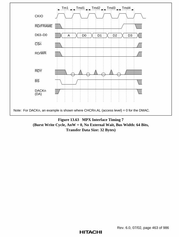
Rev. 6.0, 07/02, page 463 of 986
Tm1
CKIO
A
/
RD/
D63–D0
Tmd1 Tmd2 Tmd3 Tmd4
DACKn(DA)
D0 D1 D2 D3
Note: For DACKn, an example is shown where CHCRn.AL (access level) = 0 for the DMAC.
Figure 13.63 MPX Interface Timing 7(Burst Write Cycle, AnW = 0, No External Wait, Bus Width: 64 Bits,
Transfer Data Size: 32 Bytes)

Rev. 6.0, 07/02, page 464 of 986
D2D1
Tm1
CKIO
A
/
RD/
D63–D0
Tmd1w Tmd1 Tmd2w Tmd2 Tmd3 Tmd4w Tmd4
DACKn(DA)
D3D0
Note: For DACKn, an example is shown where CHCRn.AL (access level) = 0 for the DMAC.
Figure 13.64 MPX Interface Timing 8(Burst Write Cycle, AnW = 1, External Wait Control, Bus Width: 64 Bits,
Transfer Data Size: 32 Bytes)

Rev. 6.0, 07/02, page 465 of 986
Tm1
CKIO
A
/
RD/
D31–D0
Tmd1w Tmd1 Tmd2
DACKn(DA)
D1D0
Note: For DACKn, an example is shown where CHCRn.AL (access level) = 0 for the DMAC.
Figure 13.65 MPX Interface Timing 1(Burst Read Cycle, AnW = 0, No External Wait, Bus Width: 32 Bits,
Transfer Data Size: 64 Bytes)

Rev. 6.0, 07/02, page 466 of 986
Tm1
CKIO
A
/
RD/
D31–D0
Tmd1w Tmd1w Tmd1 Tmd2
DACKn(DA)
D1D0
Note: For DACKn, an example is shown where CHCRn.AL (access level) = 0 for the DMAC.
Figure 13.66 MPX Interface Timing 2(Burst Read Cycle, AnW = 0, One External Wait Inserted, Bus Width: 32 Bits,
Transfer Data Size: 64 Bytes)

Rev. 6.0, 07/02, page 467 of 986
Tm1
CKIO
A
/
RD/
D31–D0
Tmd1 Tmd2
DACKn(DA)
D0 D1
Note: For DACKn, an example is shown where CHCRn.AL (access level) = 0 for the DMAC.
Figure 13.67 MPX Interface Timing 3(Burst Write Cycle, AnW = 0, No External Wait, Bus Width: 32 Bits,
Transfer Data Size: 64 Bytes)
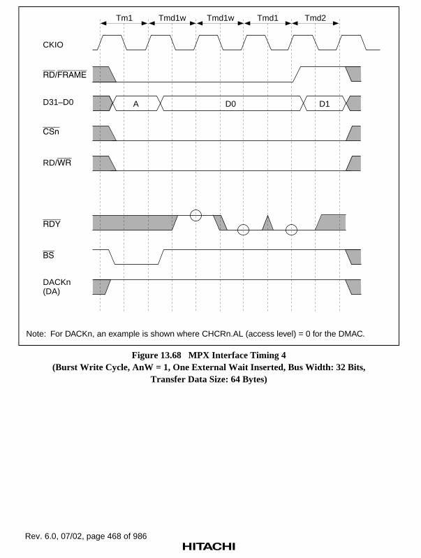
Rev. 6.0, 07/02, page 468 of 986
Tm1
CKIO
A
/
RD/
D31–D0
Tmd1w Tmd1w Tmd1 Tmd2
DACKn(DA)
D0 D1
Note: For DACKn, an example is shown where CHCRn.AL (access level) = 0 for the DMAC.
Figure 13.68 MPX Interface Timing 4(Burst Write Cycle, AnW = 1, One External Wait Inserted, Bus Width: 32 Bits,
Transfer Data Size: 64 Bytes)

Rev. 6.0, 07/02, page 469 of 986
Tm
1
CK
IO /
RD
/
D31
–D0
Tm
d1w
Tm
d1T
md2
Tm
d3T
md4
Tm
d5T
md6
Tm
d7T
md8
DA
CK
n(D
A)
D1
D2
D3
D0
D5
D6
D7
D4
A
Not
e: F
or D
AC
Kn,
an
exam
ple
is s
how
n w
here
CH
CR
n.A
L (a
cces
s le
vel)
= 0
for
the
DM
AC
.
Figure 13.69 MPX Interface Timing 5 (Burst Read Cycle, AnW = 0, No External Wait,Bus Width: 32 Bits, Transfer Data Size: 32 Bytes)

Rev. 6.0, 07/02, page 470 of 986
Tm
1
CK
IO
A
/
RD
/
D31
–D0
Tm
d1w
Tm
d1T
md2
wT
md2
Tm
d3T
md7
Tm
d8w
Tm
d8
DA
CK
n(D
A)
D6
D7
D1
D2
D0
Not
e: F
or D
AC
Kn,
an
exam
ple
is s
how
n w
here
CH
CR
n.A
L (a
cces
s le
vel)
= 0
for
the
DM
AC
.
Figure 13.70 MPX Interface Timing 6(Burst Read Cycle, AnW = 0, External Wait Control, Bus Width: 32 Bits,
Transfer Data Size: 32 Bytes)

Rev. 6.0, 07/02, page 471 of 986
Tm
1
CK
IO
A
/
RD
/
D31
–D0
Tm
d1T
md2
Tm
d3T
md4
Tm
d5T
md6
Tm
d7T
md8
DA
CK
n(D
A)
D0
D1
D2
D3
D4
D5
D6
D7
Not
e: F
or D
AC
Kn,
an
exam
ple
is s
how
n w
here
CH
CR
n.A
L (a
cces
s le
vel)
= 0
for
the
DM
AC
.
Figure 13.71 MPX Interface Timing 7(Burst Write Cycle, AnW = 0, No External Wait, Bus Width: 32 Bits,
Transfer Data Size: 32 Bytes)

Rev. 6.0, 07/02, page 472 of 986
D2
D1
Tm
1
CK
IO
A
/
RD
/
D31
–D0
Tm
d1w
Tm
d1T
md2
wT
md2
Tm
d3T
md7
Tm
d8w
Tm
d8
DA
CK
n(D
A)
D0
D6
D7
Not
e: F
or D
AC
Kn,
an
exam
ple
is s
how
n w
here
CH
CR
n.A
L (a
cces
s le
vel)
= 0
for
the
DM
AC
.
Figure 13.72 MPX Interface Timing 8(Burst Write Cycle, AnW = 1, External Wait Control, Bus Width: 32 Bits,
Transfer Data Size: 32 Bytes)

Rev. 6.0, 07/02, page 473 of 986
13.3.9 Byte Control SRAM Interface
The byte control SRAM interface is a memory interface that outputs a byte select strobe (WEn) inboth read and write bus cycles. It has 16 bit data pins, and can be connected to SRAM which hasan upper byte select strobe and lower byte select strobe function such as UB and LB.
Areas 1 and 4 can be designated as byte control SRAM interface. However, when these areas areset to MPX mode, MPX mode has priority.
The byte control SRAM interface write timing is the same as for the normal SRAM interface.
In read operations, the WEn pin timing is different. In a read access, only the WE signal for thebyte being read is asserted. Assertion is synchronized with the fall of the CKIO clock, as for theWE signal, while negation is synchronized with the rise of the CKIO clock, using the same timingas the RD signal.
In 32-byte transfer such as a cache fill or copy-back, a total of 32 bytes are transferredconsecutively according to the set bus width. The first access is performed on the data for whichthere was an access request, and the remaining accesses are performed on the data at the 32-byteboundary. The bus is not released during this period.
Figure 13.73 shows an example of byte control SRAM connection to the SH7750, and figures13.74 to 13.76 show examples of byte control SRAM read cycle.

Rev. 6.0, 07/02, page 474 of 986
A18–A3
RD/D63–D48
SH7750 Series64k × 16-bit
SRAM
A15–A0
I/O15–I/O0
D15–D0
A15–A0
I/O15–I/O0
A15–A0
I/O15–I/O0
A15–A0
I/O15–I/O0
D31–D16
D47–D32
Figure 13.73 Example of 64-Bit Data Width Byte Control SRAM

Rev. 6.0, 07/02, page 475 of 986
T1 T2
CKIO
A25–A0
RD/
D63–D0(read)
DACKn(SA: IO ← memory)
DACKn(DA)
Note: For DACKn, an example is shown where CHCRn.AL (access level) = 0 for the DMAC.
Figure 13.74 Byte Control SRAM Basic Read Cycle (No Wait)

Rev. 6.0, 07/02, page 476 of 986
T1 Tw T2
CKIO
A25–A0
RD/
D63–D0(read)
DACKn(SA: IO ← memory)
DACKn(DA)
Note: For DACKn, an example is shown where CHCRn.AL (access level) = 0 for the DMAC.
Figure 13.75 Byte Control SRAM Basic Read Cycle (One Internal Wait Cycle)

Rev. 6.0, 07/02, page 477 of 986
T1 Tw Twe T2
CKIO
A25–A0
RD/
D63–D0(read)
DACKn(SA: IO ← memory)
DACKn(DA)
Note: For DACKn, an example is shown where CHCRn.AL (access level) = 0 for the DMAC.
Figure 13.76 Byte Control SRAM Basic Read Cycle (One Internal Wait + One ExternalWait)
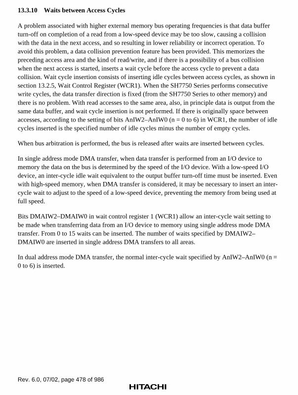
Rev. 6.0, 07/02, page 478 of 986
13.3.10 Waits between Access Cycles
A problem associated with higher external memory bus operating frequencies is that data bufferturn-off on completion of a read from a low-speed device may be too slow, causing a collisionwith the data in the next access, and so resulting in lower reliability or incorrect operation. Toavoid this problem, a data collision prevention feature has been provided. This memorizes thepreceding access area and the kind of read/write, and if there is a possibility of a bus collisionwhen the next access is started, inserts a wait cycle before the access cycle to prevent a datacollision. Wait cycle insertion consists of inserting idle cycles between access cycles, as shown insection 13.2.5, Wait Control Register (WCR1). When the SH7750 Series performs consecutivewrite cycles, the data transfer direction is fixed (from the SH7750 Series to other memory) andthere is no problem. With read accesses to the same area, also, in principle data is output from thesame data buffer, and wait cycle insertion is not performed. If there is originally space betweenaccesses, according to the setting of bits AnIW2–AnIW0 (n = 0 to 6) in WCR1, the number of idlecycles inserted is the specified number of idle cycles minus the number of empty cycles.
When bus arbitration is performed, the bus is released after waits are inserted between cycles.
In single address mode DMA transfer, when data transfer is performed from an I/O device tomemory the data on the bus is determined by the speed of the I/O device. With a low-speed I/Odevice, an inter-cycle idle wait equivalent to the output buffer turn-off time must be inserted. Evenwith high-speed memory, when DMA transfer is considered, it may be necessary to insert an inter-cycle wait to adjust to the speed of a low-speed device, preventing the memory from being used atfull speed.
Bits DMAIW2–DMAIW0 in wait control register 1 (WCR1) allow an inter-cycle wait setting tobe made when transferring data from an I/O device to memory using single address mode DMAtransfer. From 0 to 15 waits can be inserted. The number of waits specified by DMAIW2–DMAIW0 are inserted in single address DMA transfers to all areas.
In dual address mode DMA transfer, the normal inter-cycle wait specified by AnIW2–AnIW0 (n =0 to 6) is inserted.
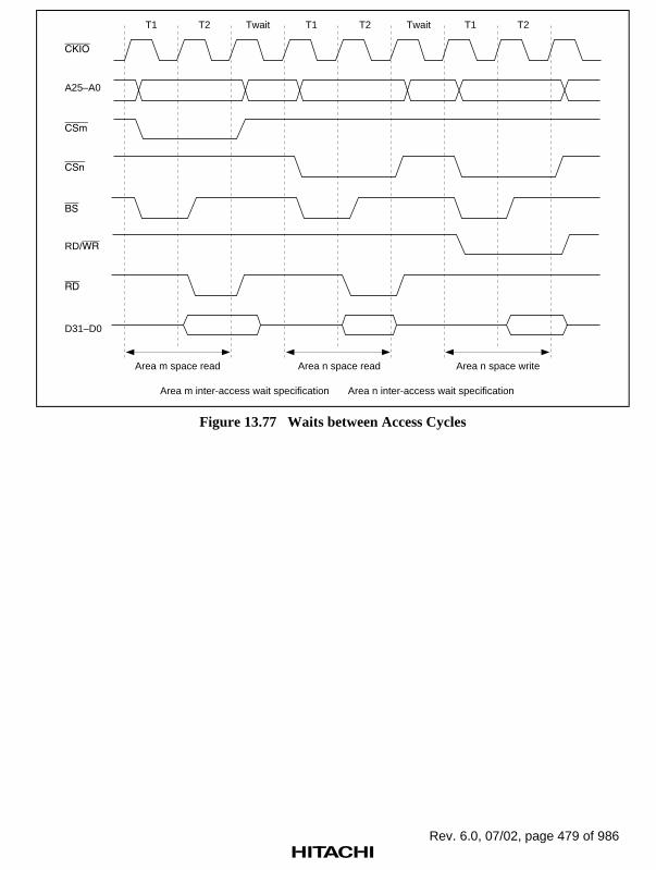
Rev. 6.0, 07/02, page 479 of 986
T1
A25–A0
RD/
D31–D0
T2 Twait T1 T2 Twait T1 T2
Area m space read
Area m inter-access wait specification Area n inter-access wait specification
Area n space read Area n space write
Figure 13.77 Waits between Access Cycles

Rev. 6.0, 07/02, page 480 of 986
13.3.11 Bus Arbitration
The SH7750 Series is provided with a bus arbitration function that grants the bus to an externaldevice when it makes a bus request.
There are three bus arbitration modes: master mode, partial-sharing master mode, and slave mode.In master mode the bus is held on a constant basis, and is released to another device in response toa bus request. In slave mode the bus is not held on a constant basis; a bus request is issued eachtime an external bus cycle occurs, and the bus is released again at the end of the access. In partial-sharing master mode, only area 2 is shared with external devices; slave mode is in effect for area2, while for other spaces, bus arbitration is not performed and the bus is held constantly. The areain the master mode chip to which area 2 in the partial-sharing master mode chip is allocated isdetermined by an external circuit.
Master mode and slave mode can be specified by the external mode pins. Partial-sharing mastermode is entered from master mode by means of a software setting. See Appendix C, Mode PinSettings, for the external mode pin settings. In master mode and slave mode, the bus goes to thehigh-impedance state when not being held. In partial-sharing master mode, the bus is constantlydriven, and therefore an external buffer is necessary for connection to the master bus. In mastermode, it is possible to connect an external device that issues bus requests instead of a slave modechip. In the following description, an external device that issues bus requests is also referred to asa slave.
The SH7750 Series has two internal bus masters: the CPU and the DMAC. When synchronousDRAM or DRAM is connected and refresh control is performed, refresh requests constitute a thirdbus master. In addition to these are bus requests from external devices in master mode. If requestsoccur simultaneously, priority is given, in high-to-low order, to a bus request from an externaldevice, a refresh request, the DMAC, and the CPU.
To prevent incorrect operation of connected devices when the bus is transferred between masterand slave, all bus control signals are negated before the bus is released. When mastership of thebus is received, also, bus control signals begin driving the bus from the negated state. Sincesignals are driven to the same value by the master and slave exchanging the bus, output buffercollisions can be avoided.
Bus transfer is executed between bus cycles.
When the bus release request signal (BREQ) is asserted, the SH7750 Series releases the bus assoon as the currently executing bus cycle ends, and outputs the bus use permission signal (BACK).However, bus release is not performed during multiple bus cycles generated because the data buswidth is smaller than the access size (for example, when performing longword access to 8-bit buswidth memory) or during a 32-byte transfer such as a cache fill or write-back. In addition, busrelease is not performed between read and write cycles during execution of a TAS instruction, orbetween read and write cycles when DMAC dual address transfer is executed. When BREQ is

Rev. 6.0, 07/02, page 481 of 986
negated, BACK is negated and use of the bus is resumed. See Appendix E, Pin Functions, for thepin states when the bus is released.
When a refresh request is generated, the SH7750 Series performs a refresh operation as soon asthe currently executing bus cycle ends. However, refresh operations are deferred during multiplebus cycles generated because the data bus width is smaller than the access size (for example, whenperforming longword access to 8-bit bus width memory) and during a 32-byte transfer such as acache fill or write-back, and also between read and write cycles during execution of a TASinstruction, and between read and write cycles when DMAC dual address transfer is executed.Refresh operations are also deferred in the bus-released state.
If the synchronous DRAM interface is set to the RAS down mode the PALL command is issuedbefore a refresh cycle occurs or before the bus is released by bus arbitration.
As the CPU in the SH7750 Series is connected to cache memory by a dedicated internal bus,reading from cache memory can still be carried out when the bus is being used by another busmaster inside or outside the SH7750 Series. When writing from the CPU, an external write cycleis generated when write-through has been set for the cache in the SH7750 Series, or when anaccess is made to a cache-off area. There is consequently a delay until the bus is returned.
When the SH7750 Series wants to take back the bus in response to an internal memory refreshrequest, it negates BACK. On receiving the BACK negation, the device that asserted the externalbus release request negates BREQ to release the bus. The bus is thereby returned to the SH7750Series, which then carries out the necessary processing.

Rev. 6.0, 07/02, page 482 of 986
HiZ
HiZ
HiZ
HiZ
HiZ
HiZ
HiZ
HiZ
HiZ
HiZ
HiZ
HiZ
HiZ
HiZ
HiZ
CKIO
HiZ
A25–A0
RD/
D63–D0 (write)
/
/
A25–A0
RD/
D63–D0 (write)
Master access Slave access Master access
Asserted for at least 2 cycles
Negated within 2 cyclesHiZ
HiZ
HiZ
HiZ
HiZ
HiZ
Master mode device access
Must be asserted for at least 2 cycles Must be negated within 2 cycles
Slave mode device access
Figure 13.78 Arbitration Sequence

Rev. 6.0, 07/02, page 483 of 986
13.3.12 Master Mode
The master mode processor holds the bus itself unless it receives a bus request.
On receiving an assertion (low level) of the bus request signal (BREQ) from off-chip, the mastermode processor releases the bus and asserts (drives low) the bus use permission signal (BACK) assoon as the currently executing bus cycle ends. If a bus release request due to a refresh request hasnot been issued, on receiving the BREQ negation (high level) indicating that the slave has releasedthe bus, the processor negates (drives high) the BACK signal and resumes use of the bus.
If a bus request is issued due to a memory refresh request in the bus-released state, the processornegates the bus use permission signal (BACK), and on receiving the BREQ negation indicatingthat the slave has released the bus, resumes use of the bus.
When the bus is released, all bus interface related output signals and input/output signals go to thehigh-impedance state, except for the synchronous DRAM interface CKE signal and bus arbitrationBACK signal, and DACK0 and DACK1 which control DMA transfers.
With DRAM, the bus is released after precharging is completed. With synchronous DRAM, also,a precharge command is issued for the active bank and the bus is released after precharging iscompleted.
The actual bus release sequence is as follows.
First, the bus use permission signal is asserted in synchronization with the rising edge of the clock.The address bus and data bus go to the high-impedance state in synchronization with the nextrising edge of the clock after this BACK assertion. At the same time, the bus control signals (BS,CSn, RAS1, RAS2, WEn, RD, RD/WR, RD2, RD/WR2, CE2A, and CE2B) go to the high-impedance state. These bus control signals are negated no later than one cycle before going tohigh-impedance. Bus request signal sampling is performed on the rising edge of the clock.
The sequence for re-acquiring the bus from the slave is as follows.
As soon as BREQ negation is detected on the rising edge of the clock, BACK is negated and buscontrol signal driving is started. Driving of the address bus and data bus starts at the next risingedge of an in-phase clock. The bus control signals are asserted and the bus cycle is actuallystarted, at the earliest, at the clock rising edge at which the address and data signals are driven.
In order to reacquire the bus and start execution of a refresh operation or bus access, the BREQsignal must be negated for at least two cycles.
If a refresh request is generated when BACK has been asserted and the bus has been released, theBACK signal is negated even while the BREQ signal is asserted to request the slave to relinquishthe bus. When the SH7750 Series is used in master mode, consecutive bus accesses may beattempted to reduce the overhead due to arbitration in the case of a slave designed independently

Rev. 6.0, 07/02, page 484 of 986
by the user. When connecting a slave for which the total duration of consecutive accesses exceedsthe refresh cycle, the design should provide for the bus to be released as soon as possible afternegation of the BACK signal is detected.
13.3.13 Slave Mode
In slave mode, the bus is normally in the released state, and an external device cannot be accessedunless the bus is acquired through execution of the bus arbitration sequence. In a reset, also, thebus-released state is established and the bus arbitration sequence is started from the reset vectorfetch.
To acquire the bus, the slave device asserts (drives low) the BSREQ signal in synchronizationwith the rising edge of the clock. The bus use permission BSACK signal is sampled for assertion(low level) in synchronization with the rising edge of the clock. When BSACK assertion isdetected, the bus control signals and address bus are immediately driven at the negated level. Thebus cycle is started at the next rising edge of the clock. The last signal negated at the end of theaccess cycle is synchronized with the rising edge of the clock. When the bus cycle ends, theBSREQ signal is negated and the release of the bus is reported to the master. On the next risingedge of the clock, the control signals are set to high-impedance.
In order for the slave mode processor to begin access, the BSACK signal must be asserted for atleast two cycles.
For a slave access cycle in DRAM or synchronous DRAM, the bus is released on completion ofprecharging, as in the case of the master.
Refresh control is left to the master mode device, and any refresh control settings made in slavemode are ignored.
Do not use DRAM/synchronous DRAM RAS down mode in slave mode.
Synchronous DRAM mode register settings should be made by the master mode device. Do notuse the DMAC’s DDT mode in slave mode.

Rev. 6.0, 07/02, page 485 of 986
13.3.14 Partial-Sharing Master Mode
In partial-sharing master mode, area 2 only is shared with other devices, and other areas can beaccessed at all times. Partial-sharing master mode can be set by setting master mode with theexternal mode pins, and setting the PSHR bit to 1 in BCR1 in the initialization procedure in apower-on reset. In a manual reset the bus state controller setting register values are retained, andso need not be set again.
Partial-sharing master mode is designed for use in conjunction with a master mode chip. Thepartial-sharing master can access a device on the master side via area 2, but the master cannotaccess a device on the partial-sharing master side.
An address and control signal buffer and a data buffer must be located between the partial-sharingmaster and the master, and controlled by a buffer control circuit.
The partial-sharing master mode processor uses the following procedure to access area 2. It assertsthe BSREQ signal on the rising edge of the clock, and issues a bus request to the master. Itsamples BSACK on each rising edge of the clock, and on receiving BSACK assertion, starts theaccess cycle on the next rising edge of the clock. At the end of the access, it negates BSREQ onthe rising edge of the clock. Buffer control in an access to an area 2 device by the partial-sharingmaster is carried out by referencing the CS2 signal or BSREQ and BSACK signals on the partial-sharing master side. Permission to use the bus is reported by the BSACK line connected to thepartial-sharing master, but the master may also negate the BSACK signal even while the bus isbeing used, if it needs the bus urgently in order to service a refresh, for example. Consequently,the partial-sharing master has to monitor the BSREQ signal to see whether it can continue to usethe bus after detecting BSACK assertion. In the case of the address buffer, after the address bufferis turned on when BSACK assertion is detected, the buffer is kept on until BSREQ is negated, atwhich point it is turned off. If the turning-off of the buffer used is late, resulting in a collision withthe start of an access cycle on the master side, the BSREQ signal output from the partial-sharingmaster must be routed through a delay circuit as part of the buffer control circuit, and input to themaster BREQ signal.
In order for a partial-sharing master mode processor to begin area 2 access, the BSACK signalmust be asserted for at least two cycles.
When the bus is released after area 2 has been accessed in partial-sharing master mode, if area 2 issynchronous DRAM, there is a wait of the period required for auto-precharge before bus release isperformed.
In partial-sharing master mode, refreshing is not performed for area 2 (refresh requests areignored).
Do not use DRAM/synchronous DRAM RAS down mode in partial-sharing master mode.

Rev. 6.0, 07/02, page 486 of 986
Area 2 synchronous DRAM mode register settings should be made by the master mode device. Setpartial-sharing master mode (by setting the PSHR bit to 1 in BCR1) after completion of the area 3synchronous DRAM mode register settings.
In partial-sharing master mode, DMA transfer should not be performed on area 2, and theDMAC’s DDT mode should not be used.
13.3.15 Cooperation between Master and Slave
To enable system resources to be controlled in a harmonious fashion by master and slave, theirrespective roles must be clearly defined. Before DRAM or synchronous DRAM is used,initialization operations must be carried out. Responsibility must also be assigned when a standbyoperation is performed to implement the power-down state.
The design of the SH7750 Series provides for all control, including initialization, refreshing, andstandby control, to be carried out by the master mode device. In a dual-processor configurationusing direct master/slave connection, all processing except direct access to memory is handled bythe master. In a combination of master mode and partial-sharing master mode, the partial-sharingmaster mode processor performs initialization, refreshing, and standby control for the areasconnected to it, with the exception of area 2, while the master performs initialization of thememory connected to it.
If the SH7750 Series is specified as the master in a power-on reset, it will not accept bus requestsfrom the slave until the BREQ enable bit (BCR1.BREQEN) is set to 1.
To ensure that the slave processor does not access memory requiring initialization before use, suchas DRAM and synchronous DRAM, until initialization is completed, write 1 to the BREQ enablebit after initialization ends.
Before setting self-refresh mode in standby mode, etc., write 0 to the BREQ enable bit toinvalidate the BREQ signal from the slave. Write 1 to the BREQ enable bit only after the masterhas performed the necessary processing (refresh settings, etc.) for exiting self-refresh mode.

Rev. 6.0, 07/02, page 487 of 986
13.3.16 Notes on Usage
Refresh: Auto refresh operations stop when a transition is made to standby mode, hardwarestandby mode or deep-sleep mode. If the memory system requires refresh operations, set thememory in the self-refresh state prior to making the transition to standby mode, hardware standbymode or deep-sleep mode.
Bus Arbitration: On transition to standby mode or deep-sleep mode, the processor in mastermode does not release bus privileges. In systems performing bus arbitration, make the transition tostandby mode or deep-sleep mode only after setting the bus privilege release enable bit(BCR1.BREQEN) to 0 for the processor in master mode. If the bus privilege release enable bitremains set to 1, operation cannot be guaranteed when the transition is made to standby mode ordeep-sleep mode.
Synchronous DRAM Mode Register Setting (SH7750, SH7750S Only): The followingconditions must be satisfied when setting the synchronous DRAM mode register.
• The DMAC must not be activated until synchronous DRAM mode register setting iscompleted.*1
• Register setting for the on-chip peripheral modules*2 must not be performed until synchronousDRAM mode register setting is completed.*3
Notes: *1 If a conflict occurs between synchronous DRAM mode register setting and memoryaccess using the DMAC, neither operation can be guaranteed.
*2 This applies to the following on-chip peripheral modules: CPG, RTC, INTC, TMU,SCI, SCIF, and H-UDI.
*3 If synchronous DRAM mode register setting is performed immediately following writeaccess to the on-chip peripheral modules*2, the values written to the on-chip peripheralmodules cannot be guaranteed.

Rev. 6.0, 07/02, page 488 of 986

Rev. 6.0, 07/02, page 489 of 986
Section 14 Direct Memory Access Controller (DMAC)
14.1 Overview
The SH7750 and SH7750S include an on-chip four-channel direct memory access controller(DMAC). The SH7750R includes an on-chip eight-channel DMAC. The DMAC can be used inplace of the CPU to perform high-speed data transfers among external devices equipped withDACK (TMU, SCI, SCIF), external memories, memory-mapped external devices, and on-chipperipheral modules (except the DMAC, BSC, and UBC). Using the DMAC reduces the burden onthe CPU and increases the operating efficiency of the chip. When using the SH7750R, see thefollowing sections:
Section 14.6, Configuration of DMAC (SH7750R);Section 14.7, Register Descriptions (SH7750R);Section 14.8, Operation (SH7750R).
14.1.1 Features
The DMAC has the following features.
• Four channels (SH7750/SH7750S), eight channels (SH7750R)
• Physical address space
• Choice of 8-bit, 16-bit, 32-bit, 64-bit, or 32-byte transfer data length
• Maximum of 16 M (16,777,216) transfers
• Choice of single or dual address mode
Single address mode: Either the transfer source or the transfer destination (external device)is accessed by a DACK signal while the other is accessed by address. One data transfer iscompleted in one bus cycle.
Dual address mode: Both the transfer source and transfer destination are accessed byaddress. Values set in DMAC internal registers indicate the accessed address for both thetransfer source and the transfer destination. Two bus cycles are required for one datatransfer.
• Choice of bus mode: Cycle steal mode or burst mode
• Two types of DMAC channel priority ranking:
Fixed priority mode: Channel priorities are permanently fixed.
Round robin mode: Sets the lowest priority for the channel for which an execution requestwas last accepted.
• An interrupt request can be sent to the CPU on completion of the specified number oftransfers.

Rev. 6.0, 07/02, page 490 of 986
• Transfer requests: The following three DMAC transfer activation requests are supported.
External request
(1) Normal DMA mode
From two DREQ pins. Either low level detection or falling edge detection can bespecified. External requests can be accepted on channels 0 and 1 only.
(2) On-demand data transfer mode (DDT mode)
In this mode of the SH7750 and SH7750S, interfacing between an external device andthe DMAC is performed using the DBREQ, BAVL, TR, TDACK, ID [1:0], and D[63:0] pins. External requests can be accepted on all four channels.
In the SH7750R, the DBREQ, BAVL, TR, TDACK, ID [2:0], and D [63:0] pins areused as the interface between an external device and the DMAC. External requests canbe accepted on any of the eight channels.
For channel 0, data transfer can be carried out with the transfer mode, number oftransfers, transfer address (single only), etc., specified by the external device.
Although channel 0 has no request queue, there are four request queues for each of theother channels: i.e., channels 1 to 3 in the SH7750 or SH7750S, and channels 1 to 7 inthe SH7750R.
In the SH7750R, request queues can be cleared on a channel-by-channel basis in DDTmode in either of the following two ways.
• Clearing a request queue by DTR formatThe request queues of the relevant channel are cleared when it receives DTR.SZ =110, DTR.ID = 00, DTR.MD = 11, and DTR.COUNT [7:4]* = [1–8].
• Using software to clear the request queueThe request queues of the relevant channel are cleared by writing a 1 to theCHCRn.QCL bit (request-queue clear bit) of each channel.
Note: * DTR.COUNT [7:4] (DTR [55:52]): Sets the port as not used.
Requests from on-chip peripheral modules
Transfer requests from the SCI, SCIF, and TMU. These can be accepted on all channels.
Auto-request
The transfer request is generated automatically within the DMAC.
• Channel functions: Transfer modes that can be set are different for each channel.
Normal DMA mode
• Channel 0: Single or dual address mode. External requests are accepted.
• Channel 1: Single or dual address mode. External requests are accepted.
• Channel 2: Dual address mode only.
• Channel 3: Dual address mode only.
• Channel 4 (SH7750R only): Dual address mode only.
• Channel 5 (SH7750R only): Dual address mode only.

Rev. 6.0, 07/02, page 491 of 986
• Channel 6 (SH7750R only): Dual address mode only.
• Channel 7 (SH7750R only): Dual address mode only.
DDT mode channel function
• Channel 0: Single address mode. External requests are acceptedDual address mode (SH7750S, SH7750R)
• Channel 1: Single or dual address mode. External requests are accepted.
• Channel 2: Single or dual address mode. External requests are accepted.
• Channel 3: Single or dual address mode. External requests are accepted.
• Channel 4 (SH7750R only): Single or dual address mode. External requests areaccepted.
• Channel 5 (SH7750R only): Single or dual address mode. External requests areaccepted.
• Channel 6 (SH7750R only): Single or dual address mode. External requests areaccepted.
• Channel 7 (SH7750R only): Single or dual address mode. External requests areaccepted.

Rev. 6.0, 07/02, page 492 of 986
14.1.2 Block Diagram (SH7750, SH7750S)
Figure 14.1 shows a block diagram of the DMAC.
SARn
DARn
DMATCRn
CHCRn
DMAOR
TMUSCI, SCIF
DACK0, DACK1DRAK0, DRAK1
DMAOR: DMAC operation registerSARn: DMAC source address
registerDARn: DMAC destination address registerDMATCRn: DMAC transfer count registerCHCRn: DMAC channel control register(n: 0 to 3)
On-chipperipheral
module
Per
iphe
ral b
us
Inte
rnal
bus
DMAC module
Countcontrol
Registercontrol
Activationcontrol
Requestprioritycontrol
Businterface
32B databuffer
Bus statecontroller
CH0 CH1 CH2 CH3
Request controller
DTR command buffer
DDT module
SAR0, DAR0, DMATCR0,CHCR0 only
External bus
ID[1:0]
D[63:0]DDTMODE
DBREQ
BAVL
Request
4
48 bits
tdack
id[1:0]
DDTD
,
Ext
erna
l add
ress
/on-
chip
pe
riphe
ral m
odul
e ad
dres
s
Figure 14.1 Block Diagram of DMAC

Rev. 6.0, 07/02, page 493 of 986
14.1.3 Pin Configuration (SH7750, SH7750S)
Tables 14.1 and 14.2 show the DMAC pins.
Table 14.1 DMAC Pins
Channel Pin Name Abbreviation I/O Function
0 DMA transferrequest
DREQ0 Input DMA transfer request input fromexternal device to channel 0
DREQ acceptanceconfirmation
DRAK0 Output Acceptance of request for DMAtransfer from channel 0 to externaldevice
Notification to external device of startof execution
DMA transfer endnotification
DACK0 Output Strobe output to external device ofDMA transfer request from channel 0to external device
1 DMA transferrequest
DREQ1 Input DMA transfer request input fromexternal device to channel 1
DREQ acceptanceconfirmation
DRAK1 Output Acceptance of request for DMAtransfer from channel 1 to externaldevice
Notification to external device of startof execution
DMA transfer endnotification
DACK1 Output Strobe output to external device ofDMA transfer request from channel 1to external device

Rev. 6.0, 07/02, page 494 of 986
Table 14.2 DMAC Pins in DDT Mode
Pin Name Abbreviation I/O Function
Data bus request DBREQ(DREQ0)
Input Data bus release request from externaldevice for DTR format input
Data bus available BAVL(DRAK0)
Output Data bus release notification
Data bus can be used 2 cycles afterBAVL is asserted
Transfer request signal TR(DREQ1)
Input If asserted 2 cycles after BAVLassertion, DTR format is sent
Only TR asserted: DMA request
DBREQ and TR assertedsimultaneously: Direct request tochannel 2
DMAC strobe TDACK(DACK0)
Output Reply strobe signal for external devicefrom DMAC
Channel numbernotification
ID [1:0](DRAK1, DACK1)
Output Notification of channel number toexternal device at same time as TDACKoutput
(ID [1] = DRAK1, ID [0] = DACK1)
14.1.4 Register Configuration (SH7750, SH7750S)
Table 14.3 summarizes the DMAC registers. The DMAC has a total of 17 registers: four registersare allocated to each channel, and an additional control register is shared by all four channels.
Table 14.3 DMAC Registers
Chan-nel Name
Abbre-viation
Read/Write Initial Value P4 Address
Area 7Address
AccessSize
0 DMA sourceaddress register 0
SAR0 R/W*2 Undefined H'FFA00000 H'1FA00000 32
DMA destinationaddress register 0
DAR0 R/W*2 Undefined H'FFA00004 H'1FA00004 32
DMA transfercount register 0
DMATCR0 R/W*2 Undefined H'FFA00008 H'1FA00008 32
DMA channelcontrol register 0
CHCR0 R/W*1 *2 H'00000000 H'FFA0000C H'1FA0000C 32

Rev. 6.0, 07/02, page 495 of 986
Table 14.3 DMAC Registers (cont)
Chan-nel Name
Abbre-viation
Read/Write Initial Value P4 Address
Area 7Address
AccessSize
1 DMA sourceaddress register 1
SAR1 R/W Undefined H'FFA00010 H'1FA00010 32
DMA destinationaddress register 1
DAR1 R/W Undefined H'FFA00014 H'1FA00014 32
DMA transfercount register 1
DMATCR1 R/W Undefined H'FFA00018 H'1FA00018 32
DMA channelcontrol register 1
CHCR1 R/W*1 H'00000000 H'FFA0001C H'1FA0001C 32
2 DMA sourceaddress register 2
SAR2 R/W Undefined H'FFA00020 H'1FA00020 32
DMA destinationaddress register 2
DAR2 R/W Undefined H'FFA00024 H'1FA00024 32
DMA transfercount register 2
DMATCR2 R/W Undefined H'FFA00028 H'1FA00028 32
DMA channelcontrol register 2
CHCR2 R/W*1 H'00000000 H'FFA0002C H'1FA0002C 32
3 DMA sourceaddress register 3
SAR3 R/W Undefined H'FFA00030 H'1FA00030 32
DMA destinationaddress register 3
DAR3 R/W Undefined H'FFA00034 H'1FA00034 32
DMA transfercount register 3
DMATCR3 R/W Undefined H'FFA00038 H'1FA00038 32
DMA channelcontrol register 3
CHCR3 R/W*1 H'00000000 H'FFA0003C H'1FA0003C 32
Com-mon
DMA operationregister
DMAOR R/W*1 H'00000000 H'FFA00040 H'1FA00040 32
Notes: Longword access should be used for all control registers. If a different access width isused, reads will return all 0s and writes will not be possible.*1 Bit 1 of CHCR0–CHCR3 and bits 2 and 1 of DMAOR can only be written with 0 after
being read as 1, to clear the flags.*2 In the SH7750, writes from the CPU are masked in DDT mode, while writes from
external I/O devices using the DTR format are possible. In the SH7750S, writes fromthe CPU and writes from external I/O devices using the DTR format are possible InDDT mode.

Rev. 6.0, 07/02, page 496 of 986
14.2 Register Descriptions (SH7750, SH7750S)
14.2.1 DMA Source Address Registers 0–3 (SAR0–SAR3)
Bit: 31 30 29 28 27 26 25 24
Initial value: — — — — — — — —
R/W: R/W R/W R/W R/W R/W R/W R/W R/W
Bit: 23 0
· · · · · · · · · · · · · · · · · · · · · · · · · · · · · · · · · · · · · · · · · · · · ·
Initial value: — · · · · · · · · · · · · · · · · · · · · · · · · · · · · · · · · · · · · · · · · · · · · · —
R/W: R/W · · · · · · · · · · · · · · · · · · · · · · · · · · · · · · · · · · · · · · · · · · · · · R/W
DMA source address registers 0–3 (SAR0–SAR3) are 32-bit readable/writable registers thatspecify the source address of a DMA transfer. These registers have a counter feedback function,and during a DMA transfer they indicate the next source address. In single address mode, the SARvalue is ignored when an external device with DACK has been specified as the transfer source.
Specify a 16-bit, 32-bit, 64-bit, or 32-byte boundary address when performing a 16-bit, 32-bit, 64-bit, or 32-byte data transfer, respectively. If a different address is specified, an address error willbe detected and the DMAC will halt.
The initial value of these registers after a power-on or manual reset is undefined. They retain theirvalues in standby mode and deep sleep mode.
When transfer is performed from memory to an external device with DACK in DDT mode, DTRformat [31:0] is set in SAR0 [31:0]. For details, see Data Transfer Request Format in section14.5.2.
In the SH7750, writes from the CPU are masked in DDT mode, while writes from external I/Odevices using the DTR format are possible. In the SH7750S, writes from the CPU and writes fromexternal I/O devices using the DTR format are possible In DDT mode.

Rev. 6.0, 07/02, page 497 of 986
14.2.2 DMA Destination Address Registers 0–3 (DAR0–DAR3)
Bit: 31 30 29 28 27 26 25 24
Initial value: — — — — — — — —
R/W: R/W R/W R/W R/W R/W R/W R/W R/W
Bit: 23 0
· · · · · · · · · · · · · · · · · · · · · · · · · · · · · · · · · · · · · · · · · · · · ·
Initial value: — · · · · · · · · · · · · · · · · · · · · · · · · · · · · · · · · · · · · · · · · · · · · · —
R/W: R/W · · · · · · · · · · · · · · · · · · · · · · · · · · · · · · · · · · · · · · · · · · · · · R/W
DMA destination address registers 0–3 (DAR0–DAR3) are 32-bit readable/writable registers thatspecify the destination address of a DMA transfer. These registers have a counter feedbackfunction, and during a DMA transfer they indicate the next destination address. In single addressmode, the DAR value is ignored when a device with DACK has been specified as the transferdestination.
Specify a 16-bit, 32-bit, 64-bit, or 32-byte boundary address when performing a 16-bit, 32-bit, 64-bit, or 32-byte data transfer, respectively. If a different address is specified, an address error willbe detected and the DMAC will halt.
The initial value of these registers after a power-on or manual reset is undefined. They retain theirvalues in standby mode and deep sleep mode.
When transfer is performed from an external device with DACK to memory in DDT mode, DTRformat [31:0] is set in DAR0 [31:0]. For details, see Data Transfer Request Format in section14.5.2.
Notes: 1. When a 16-bit, 32-bit, 64-bit, or 32-byte boundary address is specified, take care withthe setting of bit 0, bits 1–0, bits 2–0, or bits 4–0, respectively. If an addressspecification that ignores boundary considerations is made, the DMAC will detect anaddress error and halt operation on all channels (DMAOR: address error flag AE = 1).The DMAC will also detect an address error and halt if an area 7 address is specified ina data transfer employing the external bus, or if the address of a nonexistent on-chipperipheral module is specified.
2. External addresses are 29-bit. As SAR[31:29] and DAR[31:29] are not used in DMAtransfers, settings of SAR[31:29] = 000 and DAR[31:29] = 000 are recommended.

Rev. 6.0, 07/02, page 498 of 986
14.2.3 DMA Transfer Count Registers 0–3 (DMATCR0–DMATCR3)
Bit: 31 30 29 28 27 26 25 24
Initial value: 0 0 0 0 0 0 0 0
R/W: R R R R R R R R
Bit: 23 22 21 20 19 18 17 16
Initial value: — — — — — — — —
R/W: R/W R/W R/W R/W R/W R/W R/W R/W
Bit: 15 14 13 12 11 10 9 8
Initial value: — — — — — — — —
R/W: R/W R/W R/W R/W R/W R/W R/W R/W
Bit: 7 6 5 4 3 2 1 0
Initial value: — — — — — — — —
R/W: R/W R/W R/W R/W R/W R/W R/W R/W
DMA transfer count registers 0–3 (DMATCR0–DMATCR3) are 32-bit readable/writable registersthat specify the transfer count for the corresponding channel (byte count, word count, longwordcount, quadword count, or 32-byte count). Specifying H'000001 gives a transfer count of 1, whileH'000000 gives the maximum setting, 16,777,216 (16M) transfers. During DMAC operation, theremaining number of transfers is shown.
Bits 31–24 of these registers are reserved; they are always read as 0, and should only be writtenwith 0.
The initial value of these registers after a power-on or manual reset is undefined. They retain theirvalues in standby mode and deep sleep mode.
In DDT mode, settings to DMATCR0[7:0] may be made from DTR format [55:48] as well. Fordetails, see Data Transfer Request Format in section 14.5.2.

Rev. 6.0, 07/02, page 499 of 986
14.2.4 DMA Channel Control Registers 0–3 (CHCR0–CHCR3)
Bit: 31 30 29 28 27 26 25 24
SSA2 SSA1 SSA0 STC DSA2 DSA1 DSA0 DTC
Initial value: 0 0 0 0 0 0 0 0
R/W: R/W R/W R/W R/W R/W R/W R/W R/W
Bit: 23 22 21 20 19 18 17 16
— — — — DS RL AM AL
Initial value: 0 0 0 0 0 0 0 0
R/W: R R R R R/W (R/W) R/W (R/W)
Bit: 15 14 13 12 11 10 9 8
DM1 DM0 SM1 SM0 RS3 RS2 RS1 RS0
Initial value: 0 0 0 0 0 0 0 0
R/W: R/W R/W R/W R/W R/W R/W R/W R/W
Bit: 7 6 5 4 3 2 1 0
TM TS2 TS1 TS0 — IE TE DE
Initial value: 0 0 0 0 0 0 0 0
R/W: R/W R/W R/W R/W R R/W R/(W) R/W
Note: The TE bit can only be written with 0 after being read as 1, to clear the flag.The RL, AM, AL, and DS bits may be absent, depending on the channel.
DMA channel control registers 0–3 (CHCR0–CHCR3) are 32-bit readable/writable registers thatspecify the operating mode, transfer method, etc., for each channel. Bits 31–28 and 27–24 indicatethe source address and destination address, respectively; these settings are only valid when thetransfer involves the CS5 or CS6 space and the relevant space has been specified as a PCMCIAinterface space. In other cases, these bits should be cleared to 0. For details of the PCMCIAinterface, see section 13.3.7, PCMCIA Interface, in section 13, Bus State Controller (BSC).
In DDT mode, CHCR0 is set according to the DTR format. (The following settings are fixed:CHCR0 [31:24] = 0, [18:16] = 0, [15:14] = 01, [13:12] = 01, [2] = 0, [1] = 0, [0] = 1)
Bits 18 and 16 are not present in CHCR2 and CHCR3. In CHCR2 and CHCR3, these bits cannotbe modified (a write value of 0 should always be used) and are always read as 0.
These registers are initialized to H'00000000 by a power-on or manual reset. They retain theirvalues in standby mode and deep sleep mode.

Rev. 6.0, 07/02, page 500 of 986
Bits 31 to 29—Source Address Space Attribute Specification (SSA2–SSA0): These bits specifythe space attribute for access to a PCMCIA interface area.
Bit 31: SSA2 Bit 30: SSA1 Bit 29: SSA0 Description
0 0 0 Reserved in PCMCIA access (Initial value)
1 Dynamic bus sizing I/O space
1 0 8-bit I/O space
1 16-bit I/O space
1 0 0 8-bit common memory space
1 16-bit common memory space
1 0 8-bit attribute memory space
1 16-bit attribute memory space
Bit 28—Source Address Wait Control Select (STC): Specifies CS5 or CS6 space wait cyclecontrol for access to a PCMCIA interface area. This bit selects the wait control register in the BSCthat performs area 5 and 6 wait cycle control.
Bit 28: STC Description
0 C5 space wait cycle selection (Initial value)
Settings of bits A5W2–A5W0 in wait control register 2 (WCR2), and bitsA5PCW1–A5PCW0, A5TED2–A5TED0, and A5TEH2–A5TEH0 in thePCMCIA control register (PCR), are selected
1 C6 space wait cycle selection
Settings of bits A6W2–A6W0 in wait control register 2 (WCR2), and bitsA6PCW1–A6PCW0, A6TED2–A6TED0, and A6TEH2–A6TEH0 in thePCMCIA control register (PCR), are selected
Note: For details, see section 13.3.7, PCMCIA Interface.

Rev. 6.0, 07/02, page 501 of 986
Bits 27 to 25—Destination Address Space Attribute Specification (DSA2–DSA0): These bitsspecify the space attribute for access to a PCMCIA interface area.
Bit 27: DSA2 Bit 26: DSA1 Bit 25: DSA0 Description
0 0 0 Reserved in PCMCIA access (Initial value)
1 Dynamic bus sizing I/O space
1 0 8-bit I/O space
1 16-bit I/O space
1 0 0 8-bit common memory space
1 16-bit common memory space
1 0 8-bit attribute memory space
1 16-bit attribute memory space
Bit 24—Destination Address Wait Control Select (DTC): Specifies CS5 or CS6 space waitcycle control for access to a PCMCIA interface area. This bit selects the wait control register inthe BSC that performs area 5 and 6 wait cycle control.
Bit 24: DTC Description
0 C5 space wait cycle selection (Initial value)
Settings of bits A5W2–A5W0 in wait control register 2 (WCR2), and bitsA5PCW1–A5PCW0, A5TED2–A5TED0, and A5TEH2–A5TEH0 in thePCMCIA control register (PCR), are selected
1 C6 space wait cycle selection
Settings of bits A6W2–A6W0 in wait control register 2 (WCR2), and bitsA6PCW1–A6PCW0, A6TED2–A6TED0, and A6TEH2–A6TEH0 in thePCMCIA control register (PCR), are selected
Note: For details, see section 13.3.7, PCMCIA Interface.
Bits 23 to 20—Reserved: These bits are always read as 0, and should only be written with 0.

Rev. 6.0, 07/02, page 502 of 986
Bit 19—DREQDREQDREQDREQ Select (DS): Specifies either low level detection or falling edge detection as thesampling method for the DREQ pin used in external request mode.
In normal DMA mode, this bit is valid only in CHCR0 and CHCR1. In DDT mode, it is valid inCHCR0–CHCR3.
Bit 19: DS Description
0 Low level detection (Initial value)
1 Falling edge detection
Note: Level detection burst mode when TM = 1 and DS = 0Edge detection burst mode when TM = 1 and DS = 1
Bit 18—Request Check Level (RL): Selects whether the DRAK signal (that notifies an externaldevice of the acceptance of DREQ) is an active-high or active-low output.
In normal DMA mode, this bit is valid only in CHCR0 and CHCR1. In DDT mode, this bit isinvalid.
Bit 18: RL Description
0 DRAK is an active-high output (Initial value)
1 DRAK is an active-low output
Bit 17—Acknowledge Mode (AM): In dual address mode, selects whether DACK is output in thedata read cycle or write cycle. In single address mode, DACK is always output regardless of thesetting of this bit.
In normal DMA mode, this bit is valid only in CHCR0 and CHCR1. In DDT mode, this bit isvalid for CHCR1 to CHCR3 in the SH7750. In the SH7750S, this bit is valid for CHCR0 toCHCR3. (DDT mode: TDACK)
Bit 17: AM Description
0 DACK is output in read cycle (Initial value)
1 DACK is output in write cycle

Rev. 6.0, 07/02, page 503 of 986
Bit 16—Acknowledge Level (AL): Specifies the DACK (acknowledge) signal as active-high oractive-low.
In normal DMA mode, this bit is valid only in CHCR0 and CHCR1. In DDT mode, this bit isinvalid.
Bit 16: AL Description
0 Active-high output (Initial value)
1 Active-low output
Bits 15 and 14—Destination Address Mode 1 and 0 (DM1, DM0): These bits specifyincrementing/decrementing of the DMA transfer destination address. The specification of thesebits is ignored when data is transferred from external memory to an external device in singleaddress mode. For channel 0, in DDT mode these bits are set to DM1 = 0 and DM0 = 1 with theDTR format.
Bit 15: DM1 Bit 14: DM0 Description
0 0 Destination address fixed (Initial value)
1 Destination address incremented (+1 in 8-bit transfer, +2 in 16-bit transfer, +4 in 32-bit transfer, +8 in 64-bit transfer, +32 in 32-byte burst transfer)
1 0 Destination address decremented (–1 in 8-bit transfer, –2 in 16-bit transfer, –4 in 32-bit transfer, –8 in 64-bit transfer, –32 in 32-byte burst transfer)
1 Setting prohibited
Bits 13 and 12—Source Address Mode 1 and 0 (SM1, SM0): These bits specifyincrementing/decrementing of the DMA transfer source address. The specification of these bits isignored when data is transferred from an external device to external memory in single addressmode. For channel 0, in DDT mode these bits are set to DM1 = 0 and DM0 = 1 with the DTRformat.
Bit 13: SM1 Bit 12: SM0 Description
0 0 Source address fixed (Initial value)
1 Source address incremented (+1 in 8-bit transfer, +2 in 16-bittransfer, +4 in 32-bit transfer, +8 in 64-bit transfer, +32 in 32-byte burst transfer)
1 0 Source address decremented (–1 in 8-bit transfer, –2 in 16-bittransfer, –4 in 32-bit transfer, –8 in 64-bit transfer, –32 in 32-byte burst transfer)
1 Setting prohibited

Rev. 6.0, 07/02, page 504 of 986
Bits 11 to 8—Resource Select 3 to 0 (RS3–RS0): These bits specify the transfer request source.
Bit 11:RS3
Bit 10:RS2
Bit 9:RS1
Bit 8:RS0 Description
0 0 0 0 External request, dual address mode*1 *4 (external addressspace → external address space) (Initial value)
1 Setting prohibited
1 0 External request, single address mode
External address space → external device*1 *3 *4
1 External request, single address mode
External device → external address space*1 *3 *4
1 0 0 Auto-request (external address space → external addressspace)*2
1 Auto-request (external address space → on-chip peripheralmodule)*2
1 0 Auto-request (on-chip peripheral module → external addressspace)*2
1 Setting prohibited
1 0 0 0 SCI transmit-data-empty interrupt transfer request(external address space → SCTDR1)*2
1 SCI receive-data-full interrupt transfer request(SCRDR1 → external address space)*2
1 0 SCIF transmit-data-empty interrupt transfer request(external address space → SCFTDR2)*2
1 SCIF receive-data-full interrupt transfer request(SCFRDR2 → external address space)*2
1 0 0 TMU channel 2 (input capture interrupt, external address space→ external address space)*2
1 TMU channel 2 (input capture interrupt, external address space→ on-chip peripheral module)*2
1 0 TMU channel 2 (input capture interrupt, on-chip peripheralmodule → external address space)*2
1 Setting prohibited
Notes: *1 External request specifications are valid only for channels 0 and 1. Requests are notaccepted for channels 2 and 3 in normal DMA mode.
*2 Dual address mode*3 In DDT mode, selection is possible with the DTR format [60] (R/W bit) and [57-56]
(MD1, MD0 bits) specification for channel 0 only.
*4 In DDT mode:[SH7750] An external request specification should be set for channels 1 to 3. For
channel 0, only single address mode can be set with the DTR format.[SH7750S] An external request specification can be set for channels 0 to 3.

Rev. 6.0, 07/02, page 505 of 986
Bit 7—Transmit Mode (TM): Specifies the bus mode for transfer.
Bit 7: TM Description
0 Cycle steal mode (Initial value)
1 Burst mode
Bits 6 to 4—Transmit Size 2 to 0 (TS2–TS0): These bits specify the transfer data size. Forexternal memory access, the setting of these bits serves as the access size in section 14.3,Operation. For register access, the setting of these bits is the size in which the register is accessed.
Bit 6: TS2 Bit 5: TS1 Bit 4: TS0 Description
0 0 0 Quadword size (64-bit) specification(Initial value)
1 Byte size (8-bit) specification
1 0 Word size (16-bit) specification
1 Longword size (32-bit) specification
1 0 0 32-byte block transfer specification
Bit 3—Reserved: This bit is always read as 0, and should only be written with 0.
Bit 2—Interrupt Enable (IE): When this bit is set to 1, an interrupt request (DMTE) is generatedafter the number of data transfers specified in DMATCR (when TE = 1).
Bit 2: IE Description
0 Interrupt request not generated after number of transfers specified inDMATCR (Initial value)
1 Interrupt request generated after number of transfers specified in DMATCR

Rev. 6.0, 07/02, page 506 of 986
Bit 1—Transfer End (TE): This bit is set to 1 after the number of transfers specified inDMATCR. If the IE bit is set to 1 at this time, an interrupt request (DMTE) is generated.
If data transfer ends before TE is set to 1 (for example, due to an NMI interrupt, address error, orclearing of the DE bit or the DME bit in DMAOR), the TE bit is not set to 1. When this bit is 1,the transfer enabled state is not entered even if the DE bit is set to 1.
Bit 1: TE Description
0 Number of transfers specified in DMATCR not completed (Initial value)
[Clearing conditions]
• When 0 is written to TE after reading TE = 1
• In a power-on or manual reset, and in standby mode
1 Number of transfers specified in DMATCR completed
Bit 0—DMAC Enable (DE): Enables operation of the corresponding channel.
Bit 0: DE Description
0 Operation of corresponding channel is disabled (Initial value)
1 Operation of corresponding channel is enabled
When auto-request is specified (with RS3–RS0), transfer is begun when this bit is set to 1. In thecase of an external request or on-chip peripheral module request, transfer is begun when a transferrequest is issued after this bit is set to 1. Transfer can be suspended midway by clearing this bit to0.
Even if the DE bit has been set, transfer is not enabled when TE is 1, when DME in DMAOR is 0,or when the NMIF or AE bit in DMAOR is 1.
For channel 0, in DDT mode this bit is set to 1 when a DTR format is received. DE remains set to1 even if TE is set to 1. When the mode is switched from DDT mode to normal DMA mode (DDTbit = 0 in DMAOR), the DE bit must be cleared to 0.

Rev. 6.0, 07/02, page 507 of 986
14.2.5 DMA Operation Register (DMAOR)
Bit: 31 30 29 28 27 26 25 24
— — — — — — — —
Initial value: 0 0 0 0 0 0 0 0
R/W: R R R R R R R R
Bit: 23 22 21 20 19 18 17 16
— — — — — — — —
Initial value: 0 0 0 0 0 0 0 0
R/W: R R R R R R R R
Bit: 15 14 13 12 11 10 9 8
DDT — — — — — PR1 PR0
Initial value: 0 0 0 0 0 0 0 0
R/W: R/W R R R R R R/W R/W
Bit: 7 6 5 4 3 2 1 0
— — — COD — AE NMIF DME
Initial value: 0 0 0 0 0 0 0 0
R/W: R R R R/(W) R R/(W) R/(W) R/W
Note: The AE and NMIF bits can only be written with 0 after being read as 1, to clear the flags.The COD bit can be written to in the SH7750S only.
DMAOR is a 32-bit readable/writable register that specifies the DMAC transfer mode.
DMAOR is initialized to H'00000000 by a power-on or manual reset. They retain their values instandby mode and deep sleep mode.
Bits 31 to 16—Reserved: These bits are always read as 0, and should only be written with 0.
Bit 15—On-Demand Data Transfer (DDT): Specifies on-demand data transfer mode.
Bit 15: DDT Description
0 Normal DMA mode (Initial value)
1 On-demand data transfer mode
Note: BAVL (DRAK0) is an active-high output in normal DMA mode. When the DDT bit is set to 1,the BAVL pin function is enabled and this pin becomes an active-low output.

Rev. 6.0, 07/02, page 508 of 986
Bits 14 to 10—Reserved: These bits are always read as 0, and should only be written with 0.
Bits 9 and 8—Priority Mode 1 and 0 (PR1, PR0): These bits determine the order of priority forchannel execution when transfer requests are made for a number of channels simultaneously.
Bit 9: PR1 Bit 8: PR0 Description
0 0 CH0 > CH1 > CH2 > CH3 (Initial value)
1 CH0 > CH2 > CH3 > CH1
1 0 CH2 > CH0 > CH1 > CH3
1 Round robin mode
Bits 7 to 5—Reserved: These bits are always read as 0, and should only be written with 0.
Bit 4 (SH7750S)—Check Overrun for DREQDREQDREQDREQ (COD): When this bit is set to 1, cancellation ofan accepted DREQ acceptance flag is enabled. When cancellation of an accepted DREQacceptance flag is enabled by setting COD to 1, clear CHCRn.DS to 0 and then negate DREQ (tothe high level). For details, see External Request Mode in section 14.3.2.
Bit 4: COD Description
0 DREQ acceptance flag cancellation disabled (Initial value)
1 DREQ acceptance flag cancellation enabled
Note: When external request mode is used in the SH7750S, recommend setting COD to 1permanently.
Bit 4 (SH7750)—Reserved: These bits are always read as 0, and should only be written with 0.
Bit 3—Reserved: This bit is always read as 0, and should only be written with 0.
Bit 2—Address Error Flag (AE): Indicates that an address error has occurred during DMAtransfer. If this bit is set during data transfer, transfers on all channels are suspended, and aninterrupt request (DMAE) is generated. The CPU cannot write 1 to AE. This bit can only becleared by writing 0 after reading 1.
Bit 2: AE Description
0 No address error, DMA transfer enabled (Initial value)
[Clearing condition]When 0 is written to AE after reading AE = 1
1 Address error, DMA transfer disabled
[Setting condition]When an address error is caused by the DMAC

Rev. 6.0, 07/02, page 509 of 986
Bit 1—NMI Flag (NMIF): Indicates that NMI has been input. This bit is set regardless ofwhether or not the DMAC is operating. If this bit is set during data transfer, transfers on allchannels are suspended. The CPU cannot write 1 to NMIF. This bit can only be cleared by writing0 after reading 1.
Bit 1: NMIF Description
0 No NMI input, DMA transfer enabled (Initial value)
[Clearing condition]When 0 is written to NMIF after reading NMIF = 1
1 NMI input, DMA transfer disabled
[Setting condition]When an NMI interrupt is generated
Bit 0—DMAC Master Enable (DME): Enables activation of the entire DMAC. When the DMEbit and the DE bit of the CHCR register for the corresponding channel are set to 1, that channel isenabled for transfer. If this bit is cleared during data transfer, transfers on all channels aresuspended.
Even if the DME bit has been set, transfer is not enabled when TE is 1 or DE is 0 in CHCR, orwhen the NMI or AE bit in DMAOR is 1.
Bit 0: DME Description
0 Operation disabled on all channels (Initial value)
1 Operation enabled on all channels

Rev. 6.0, 07/02, page 510 of 986
14.3 Operation
When a DMA transfer request is issued, the DMAC starts the transfer according to thepredetermined channel priority order. It ends the transfer when the transfer end conditions aresatisfied. Transfers can be requested in three modes: auto-request, external request, and on-chipperipheral module request. There are two modes for DMA transfer: single address mode and dualaddress mode. Either burst mode or cycle steal mode can be selected as the bus mode.
14.3.1 DMA Transfer Procedure
After the desired transfer conditions have been set in the DMA source address register (SAR),DMA destination address register (DAR), DMA transfer count register (DMATCR), DMAchannel control register (CHCR), and DMA operation register (DMAOR), the DMAC transfersdata according to the following procedure:
1. The DMAC checks to see if transfer is enabled (DE = 1, DME = 1, TE = 0, NMIF = 0, AE =0).
2. When a transfer request is issued and transfer has been enabled, the DMAC transfers onetransfer unit of data (determined by the setting of TS2–TS0). In auto-request mode, the transferbegins automatically when the DE bit and DME bit are set to 1. The DMATCR value isdecremented by 1 for each transfer. The actual transfer flow depends on the address mode andbus mode.
3. When the specified number of transfers have been completed (when the DMATCR valuereaches 0), the transfer ends normally. If the IE bit in CHCR is set to 1 at this time, a DMTEinterrupt request is sent to the CPU.
4. If a DMAC address error or NMI interrupt occurs, the transfer is suspended. Transfer is alsosuspended when the DE bit in CHCR or the DME bit in DMAOR is cleared to 0. In the eventof an address error, a DMAE interrupt request is forcibly sent to the CPU.
Figure 14.2 shows a flowchart of this procedure.
Note: If transfer request is issued while transfer is disabled, the transfer enable wait state(transfer suspended state) is entered. Transfer is started when subsequently enabled (bysetting DE = 1, DME = 1, TE = 0, NMIF = 0, AE = 0)

Rev. 6.0, 07/02, page 511 of 986
Start
Initial settings(SAR, DAR, DMATCR,
CHCR, DMAOR)
Illegal address check(reflected in AE bit)
DE, DME = 1?
NMIF, AE, TE = 0?
Transferrequest issued?
*1
Transfer (1 transfer unit)DMATCR - 1 → DMATCR
Update SAR, DAR
DMTE interrupt request(when IE = 1)
DMATCR = 0?
NMIF or AE = 1 or DE = 0 or
DME = 0?
End of transfer Normal end
NMIF or AE = 1 or DE = 0 or
DME = 0?
Bus mode,transfer request mode,
detectionmethod
Transfer suspended
*4
*2
*3
No
No
Yes
Yes
Yes
No
No No
Yes
Yes
No
Yes
Notes: *1 In auto-request mode, transfer begins when the NMIF, AE, and TE bits are all 0, and the DE and DME bits are set to 1.
*2 level detection (external request) in burst mode, or cycle steal mode. *3 edge detection (external request) in burst mode, or auto-request mode in burst mode. *4 An illegal address is detected by comparing bits TS2–TS0 in CHCRn with SARn and DARn.
Figure 14.2 DMAC Transfer Flowchart

Rev. 6.0, 07/02, page 512 of 986
14.3.2 DMA Transfer Requests
DMA transfer requests are basically generated at either the data transfer source or destination, butthey can also be issued by external devices or on-chip peripheral modules that are neither thesource nor the destination.
Transfers can be requested in three modes: auto-request, external request, and on-chip peripheralmodule request. The transfer request mode is selected by means of bits RS3–RS0 in DMA channelcontrol registers 0–3 (CHCR0–CHCR3).
Auto Request Mode: When there is no transfer request signal from an external source, as in amemory-to-memory transfer or a transfer between memory and an on-chip peripheral moduleunable to request a transfer, the auto-request mode allows the DMAC to automatically generate atransfer request signal internally. When the DE bit in CHCR0–CHCR3 and the DME bit in theDMA operation register (DMAOR) are set to 1, the transfer begins (so long as the TE bit inCHCR0–CHCR3 and the NMIF and AE bits in DMAOR are all 0).
External Request Mode: In this mode a transfer is performed in response to a transfer requestsignal (DREQ) from an external device. One of the modes shown in table 14.4 should be chosenaccording to the application system. If DMA transfer is enabled (DE = 1, DME = 1, TE = 0, NMIF= 0, AE = 0), transfer starts when DREQ is input. The DS bit in CHCR0/CHCR1 is used to selecteither falling edge detection or low level detection for the DREQ signal (level detection when DS= 0, edge detection when DS = 1).
The source of the transfer request does not have to be the data transfer source or destination.
DREQ is accepted after a power-on reset if TE = 0, NMIF = 0, and AE = 0, but transfer is not
executed if DMA transfer is not enabled (DE = 0 or DME = 0).
In this case, DMA transfer is started when enabled (by setting DE = 1 and DME = 1).

Rev. 6.0, 07/02, page 513 of 986
Table 14.4 Selecting External Request Mode with RS Bits
RS3 RS2 RS1 RS0 Address Mode Transfer Source Transfer Destination
0 0 0 0 Dual addressmode
External memoryor memory-mappedexternal device, orexternal device withDACK
External memoryor memory-mappedexternal device, orexternal device withDACK
1 0 Single addressmode
External memoryor memory-mappedexternal device
External devicewith DACK
1 Single addressmode
External device withDACK
External memoryor memory-mappedexternal device
• External Request Acceptance Conditions
1. When at least one of DMAOR.DME and CHCR.DE is 0, and DMAOR.NMIF,DMAOR.AE, and CHCR.TE are all 0, if an external request (DREQ: edge-detected) isinput it will be held inside the DMAC until DMA transfer is either executed or canceled.Since DMA transfer is not enabled in this case (DME = 0 or DE = 0), DMA transfer is notinitiated. DMA transfer is started after it is enabled (DME = 1, DE = 1, DMAOR.NMIF =0, DMAOR.AE = 0, CHCR.TE = 0).
2. When DMA transfer is enabled (DME = 1, DE = 1, DMAOR.NMIF = 0, DMAOR.AE = 0,CHCR.TE = 0), if an external request (DREQ) is input, DMA transfer is started.
3. An external request (DREQ) will be ignored if input when CHCR.TE = 1, DMAOR.NMIF= 1, or DMAOR.AE = 1, or during a power-on reset or manual reset, in deep sleep mode orstandby mode, or while the DMAC is in the module standby state.
4. A previously input external request will be canceled by the occurrence of an NMI interrupt(DMAOR.NMIF = 1) or address error (DMAOR.AE = 1), or by a power-on reset ormanual reset.
In the SH7750S, it is possible to cancel a previously input external request (DREQ). WithDMAOR.COD set to 1, clear CHCRn.DS to 0 and then drive the DREQ pin high.
On the SH7750R, it is possible to cancel an external request that has been accepted byexternal request (DREQ) edge detection by first negating DREQ and then clearingCHCR.DS from 1 to 0. Afterwards CHCR.DS should be reset to 1 and DREQ asserted.(The SH7750R has no DMAOR.COD bit, but it is possible to cancel an external requestthat has been accepted by external request (DREQ) edge detection, as is the case when theDMAOR.COD bit of the SH7750S is set to 1.)
• Usage Notes
An external request (DREQ) is detected by a low level or falling edge. Ensure that the externalrequest (DREQ) signal is held high when there is no DMA transfer request from an externaldevice after a power-on reset or manual reset.

Rev. 6.0, 07/02, page 514 of 986
When DMA transfer is restarted, check whether a DMA transfer request is being held.
On-Chip Peripheral Module Request Mode: In this mode a transfer is performed in response toa transfer request signal (interrupt request signal) from an on-chip peripheral module. As shown intable 14.5, there are seven transfer request signals: input capture interrupts from the timer unit(TMU), and receive-data-full interrupts (RXI) and transmit-data-empty interrupts (TXI) from thetwo serial communication interfaces (SCI, SCIF). If DMA transfer is enabled (DE = 1, DME = 1,TE = 0, NMIF = 0, AE = 0), transfer starts when a transfer request signal is input.
The source of the transfer request does not have to be the data transfer source or destination.However, when the transfer request is set to RXI (transfer request by SCI/SCIF receive-data-fullinterrupt), the transfer source must be the SCI/SCIF’s receive data register (SCRDR1/SCFRDR2).When the transfer request is set to TXI (transfer request by SCI/SCIF transmit-data-emptyinterrupt), the transfer destination must be the SCI/SCIF’s transmit data register(SCTDR1/SCFTDR2).
Table 14.5 Selecting On-Chip Peripheral Module Request Mode with RS Bits
RS3 RS2 RS1 RS0DMAC TransferRequest Source
DMAC TransferRequest Signal
TransferSource
TransferDestination Bus Mode
1 0 0 0 SCI transmitter SCTDR1 (SCItransmit-data-empty transferrequest)
External* SCTDR1 Cycle stealmode
1 SCI receiver SCRDR1 (SCIreceive-data-fulltransfer request)
SCRDR1 External* Cycle stealmode
1 0 SCIF transmitter SCFTDR2 (SCIFtransmit-data-empty transferrequest)
External* SCFTDR2 Cycle stealmode
1 SCIF receiver SCFRDR2 (SCIFreceive-data-fulltransfer request)
SCFRDR2 External* Cycle stealmode
1 0 0 TMU channel 2 Input captureoccurrence
External* External* Burst/cyclesteal mode
1 TMU channel 2 Input captureoccurrence
External* On-chipperipheral
Burst/cyclesteal mode
1 0 TMU channel 2 Input captureoccurrence
On-chipperipheral
External* Burst/cyclesteal mode
TMU: Timer unitSCI: Serial communication interface
SCIF: Serial communication interface with FIFONotes: 1. SCI/SCIF burst transfer setting is prohibited.

Rev. 6.0, 07/02, page 515 of 986
2. If input capture interrupt acceptance is set for multiple channels and DE = 1 for eachchannel, processing will be executed on the highest-priority channel in response to asingle input capture interrupt.
3. A DMA transfer request by means of an input capture interrupt can be canceled bysetting TCR2.ICPE1 = 0 and ICPE0 = 0 in the TMU.
* External memory or memory-mapped external device
To output a transfer request from an on-chip peripheral module, set the DMA transfer requestenable bit for that module and output a transfer request signal.
For details, see sections 12, Timer Unit (TMU), 15, Serial Communication Interface (SCI), and16, Serial Communication Interface with FIFO (SCIF).
When a DMA transfer corresponding to a transfer request signal from an on-chip peripheralmodule shown in table 14.5 is carried out, the signal is discontinued automatically. This occursevery transfer in cycle steal mode, and in the last transfer in burst mode.
14.3.3 Channel Priorities
If the DMAC receives simultaneous transfer requests on two or more channels, it selects a channelaccording to a predetermined priority system, either in a fixed mode or round robin mode. Themode is selected with priority bits PR1 and PR0 in the DMA operation register (DMAOR).
Fixed Mode: In this mode, the relative channel priorities remain fixed. The following priorityorders are available in fixed mode:
• CH0 > CH1 > CH2 > CH3
• CH0 > CH2 > CH3 > CH1
• CH2 > CH0 > CH1 > CH3
The priority order is selected with bits PR1 and PR0 in DMAOR.
Round Robin Mode: In round robin mode, each time the transfer of one transfer unit (byte, word,longword, quadword, or 32 bytes) ends on a given channel, that channel is assigned the lowestpriority level. This is illustrated in figure 14.3. The order of priority in round robin modeimmediately after a reset is CH0 > CH1 > CH2 > CH3.
Note: In round robin mode, if no transfer request is accepted for any channel during DMAtransfer, the priority order becomes CH0 > CH1 > CH2 > CH3.

Rev. 6.0, 07/02, page 516 of 986
CH0 > CH1 > CH2 > CH3
CH1 > CH2 > CH3 > CH0
CH0 > CH1 > CH2 > CH3
Transfer on channel 0
Priority order after transfer
Initial priority order Channel 0 is given the lowest priority.
Transfer on channel 1
Priority order after transfer
Initial priority order
Transfer on channel 2
Priority order after transfer
Initial priority order
Priority after transfer due to issuance of a transfer request for channel 1 only.
When channel 2 is given the lowest priority, the priorities of channels 0 and 1, which were higher than channel 2, are also shifted simultaneously. If there is a transfer request for channel 1 only immediately afterward, channel 1 is given the lowest priority and the priorities of channels 3 and 0 are simultaneously shifted down.
Transfer on channel 3
Initial priority order
Priority order after transfer
No change in priority order
CH0 > CH1 > CH2 > CH3
CH3 > CH0 > CH1 > CH2
CH2 > CH3 > CH0 > CH1
CH0 > CH1 > CH2 > CH3
CH0 > CH1 > CH2 > CH3
CH2 > CH3 > CH0 > CH1
When channel 1 is given the lowest priority, the priority of channel 0, which was higher than channel 1, is also shifted simultaneously.
Figure 14.3 Round Robin Mode
Figure 14.4 shows the changes in priority levels when transfer requests are issued simultaneouslyfor channels 0 and 3, and channel 1 receives a transfer request during a transfer on channel 0. Theoperation of the DMAC in this case is as follows.

Rev. 6.0, 07/02, page 517 of 986
1. Transfer requests are issued simultaneously for channels 0 and 3.
2. Since channel 0 has a higher priority level than channel 3, the channel 0 transfer is executedfirst (channel 3 is on transfer standby).
3. A transfer request is issued for channel 1 during the channel 0 transfer (channels 1 and 3 are ontransfer standby).
4. At the end of the channel 0 transfer, channel 0 shifts to the lowest priority level.
5. At this point, channel 1 has a higher priority level than channel 3, so the channel 1 transfer isstarted (channel 3 is on transfer standby).
6. At the end of the channel 1 transfer, channel 1 shifts to the lowest priority level.
7. The channel 3 transfer is started.
8. At the end of the channel 3 transfer, the channel 3 and channel 2 priority levels are lowered,giving channel 3 the lowest priority.
3
1, 3
3
Transfer request Channelwaiting
DMAC operation Channel priorityorder
1. Issued for channels 0 and 3
3. Issued for channel 1
2. Start of channel 0 transfer
0 > 1 > 2 > 3
1 > 2 > 3 > 0
2 > 3 > 0 > 1
0 > 1 > 2 > 3
4. End of channel 0 transfer
5. Start of channel 1 transfer
6. End of channel 1 transfer
7. Start of channel 3 transfer
8. End of channel 3 transfer
Change of priority order
Change of priority order
Change of priority order
None
Figure 14.4 Example of Changes in Priority Order in Round Robin Mode

Rev. 6.0, 07/02, page 518 of 986
14.3.4 Types of DMA Transfer
The DMAC supports the transfers shown in table 14.6. It can operate in single address mode, inwhich either the transfer source or the transfer destination is accessed using the acknowledgesignal, or in dual address mode, in which both the transfer source and transfer destinationaddresses are output. The actual transfer operation timing depends on the bus mode, which can beeither burst mode or cycle steal mode.
Table 14.6 Supported DMA Transfers
Transfer Destination
Transfer SourceExternal Devicewith DACK
ExternalMemory
Memory-MappedExternal Device
On-ChipPeripheral Module
External devicewith DACK
Not available Single addressmode
Single addressmode
Not available
External memory Single addressmode
Dual addressmode
Dual address mode Dual address mode
Memory-mappedexternal device
Single addressmode
Dual addressmode
Dual address mode Dual address mode
On-chip peripheralmodule
Not available Dual addressmode
Dual address mode Not available

Rev. 6.0, 07/02, page 519 of 986
Address Modes
Single Address Mode: In single address mode, both the transfer source and the transferdestination are external; one is accessed by the DACK signal and the other by an address. In thismode, the DMAC performs a DMA transfer in one bus cycle by simultaneously outputting theexternal device strobe signal (DACK) to either the transfer source or transfer destination externaldevice to access it, while outputting an address to the other side of the transfer. Figure 14.5 showsan example of a transfer between external memory and an external device with DACK in whichthe external device outputs data to the data bus and that data is written to external memory in thesame bus cycle.
DMAC
DACK
Externalmemory
External devicewith DACK
SH7750 Series
External address bus
: Data flow
External data bus
Figure 14.5 Data Flow in Single Address Mode
Two types of transfer are possible in single address mode: (1) transfer between an external devicewith DACK and a memory-mapped external device, and (2) transfer between an external devicewith DACK and external memory. Only the external request signal (DREQ) is used in both thesecases.
Figure 14.6 shows the DMA transfer timing for single address mode.
The access timing depends on the type of external memory. For details, see the descriptions of thememory interfaces in section 13, Bus State Controller (BSC).
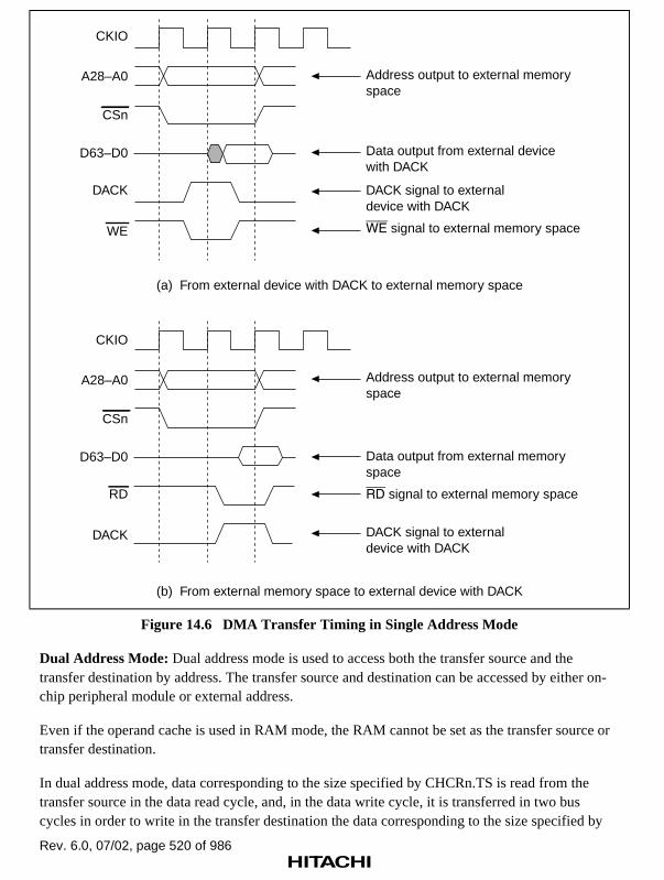
Rev. 6.0, 07/02, page 520 of 986
Address output to external memory space
Data output from external device with DACK
DACK signal to external device with DACK
signal to external memory space
Address output to external memory space
Data output from external memory space
signal to external memory space
DACK signal to external device with DACK
(a) From external device with DACK to external memory space
(b) From external memory space to external device with DACK
CKIO
A28–A0
CSn
D63–D0
DACK
WE
CKIO
A28–A0
CSn
D63–D0
RD
DACK
Figure 14.6 DMA Transfer Timing in Single Address Mode
Dual Address Mode: Dual address mode is used to access both the transfer source and thetransfer destination by address. The transfer source and destination can be accessed by either on-chip peripheral module or external address.
Even if the operand cache is used in RAM mode, the RAM cannot be set as the transfer source ortransfer destination.
In dual address mode, data corresponding to the size specified by CHCRn.TS is read from thetransfer source in the data read cycle, and, in the data write cycle, it is transferred in two buscycles in order to write in the transfer destination the data corresponding to the size specified by
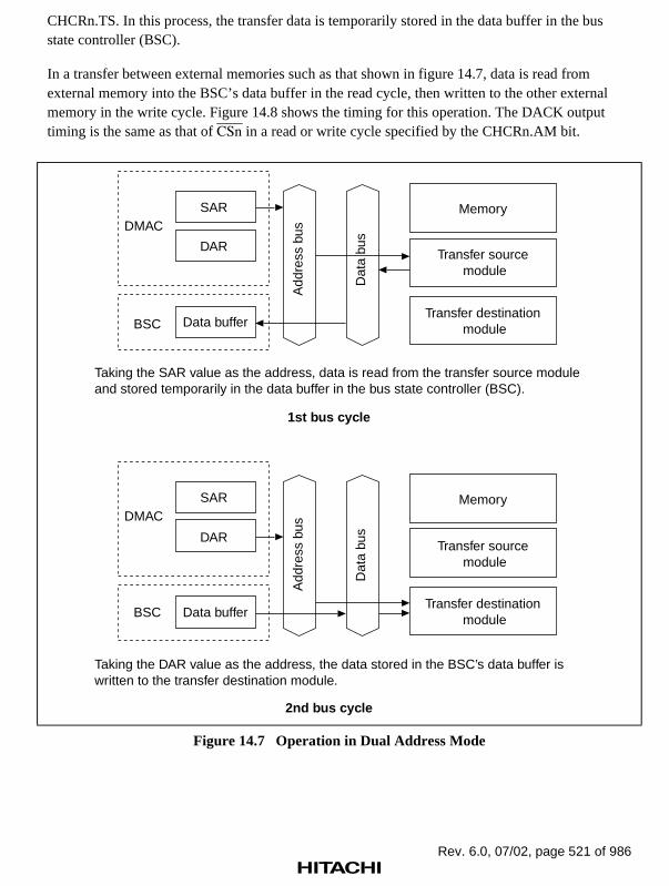
Rev. 6.0, 07/02, page 521 of 986
CHCRn.TS. In this process, the transfer data is temporarily stored in the data buffer in the busstate controller (BSC).
In a transfer between external memories such as that shown in figure 14.7, data is read fromexternal memory into the BSC’s data buffer in the read cycle, then written to the other externalmemory in the write cycle. Figure 14.8 shows the timing for this operation. The DACK outputtiming is the same as that of CSn in a read or write cycle specified by the CHCRn.AM bit.
Data buffer
Add
ress
bus
Dat
a bu
s
Add
ress
bus
Dat
a bu
s
Memory
Transfer source module
Transfer destination module
Memory
Transfer source module
Transfer destination module
SAR
DAR
Data buffer
SAR
DAR
Taking the SAR value as the address, data is read from the transfer source module and stored temporarily in the data buffer in the bus state controller (BSC).
1st bus cycle
2nd bus cycle
Taking the DAR value as the address, the data stored in the BSC’s data buffer is written to the transfer destination module.
DMAC
BSC
BSC
DMAC
Figure 14.7 Operation in Dual Address Mode

Rev. 6.0, 07/02, page 522 of 986
CKIO
A26–A0
D63–D0
DACK
Transfer from external memory space to external memory space
Transfer sourceaddress
Transfer destinationaddress
Data read cycle (1st cycle)
Data write cycle(2nd cycle)
Figure 14.8 Example of Transfer Timing in Dual Address Mode
Bus Modes
There are two bus modes, cycle steal mode and burst mode, selected with the TM bit in CHCR0–CHCR3.
Cycle Steal Mode: In cycle steal mode, the DMAC releases the bus to the CPU at the end of eachtransfer-unit (8-bit, 16-bit, 32-bit, 64-bit, or 32-byte) transfer. When the next transfer request isissued, the DMAC reacquires the bus from the CPU and carries out another transfer-unit transfer.At the end of this transfer, the bus is again given to the CPU. This is repeated until the transfer endcondition is satisfied.
Cycle steal mode can be used with all categories of transfer request source, transfer source, andtransfer destination.
Figure 14.9 shows an example of DMA transfer timing in cycle steal mode. The transferconditions in this example are dual address mode and DREQ level detection.

Rev. 6.0, 07/02, page 523 of 986
CPUCPUDMACDMACCPUDMACDMACCPUCPUCPUBus cycle
Bus returned to CPU
Read Write Read Write
Figure 14.9 Example of DMA Transfer in Cycle Steal Mode
Burst Mode: In burst mode, once the DMAC has acquired the bus it holds the bus and transfersdata continuously until the transfer end condition is satisfied. With DREQ low level detection inexternal request mode, however, when DREQ is driven high the bus passes to another bus masterafter the end of the DMAC transfer request that has already been accepted, even if the transfer endcondition has not been satisfied.
Figure 14.10 shows an example of DMA transfer timing in burst mode. The transfer conditions inthis example are single address mode and DREQ level detection (CHCRn.DS = 0, CHCRn.TM =1).
CPUDMACDMACDMACDMACDMACDMACCPUCPUCPUBus cycle
Figure 14.10 Example of DMA Transfer in Burst Mode
Note: Burst mode can be set regardless of the transfer size. A 32-byte block transfer burst modesetting can also be made.
Relationship between DMA Transfer Type, Request Mode, and Bus Mode
Table 14.7 shows the relationship between the type of DMA transfer, the request mode, and thebus mode.

Rev. 6.0, 07/02, page 524 of 986
Table 14.7 Relationship between DMA Transfer Type, Request Mode, and Bus Mode
AddressMode Type of Transfer
RequestMode
BusMode
Transfer Size(Bits)
UsableChannels
Single External device with DACKand external memory
External B/C 8/16/32/64/32B 0, 1 (2, 3)*6
External device with DACKand memory-mappedexternal device
External B/C 8/16/32/64/32B 0, 1 (2, 3)*6
Dual External memory andexternal memory
Internal*1
External*7B/C 8/16/32/64/32B 0, 1, 2, 3*5 *6
External memory andmemory-mapped externaldevice
Internal*1
External*7B/C 8/16/32/64/32B 0, 1, 2, 3*5 *6
Memory-mapped externaldevice and memory-mappedexternal device
Internal*1
External*7B/C 8/16/32/64/32B 0, 1, 2, 3*5 *6
External memory andon-chip peripheral module
Internal*2 B/C*3 8/16/32/64*4 0, 1, 2, 3*5 *6
Memory-mapped externaldevice and on-chipperipheral module
Internal*2 B/C*3 8/16/32/64*4 0, 1, 2, 3*5 *6
32B: 32-byte burst transfer
B: BurstC: Cycle stealExternal: External request
Internal: Auto-request or on-chip peripheral module request
Notes: *1 External request, auto-request, or on-chip peripheral module request (TMU inputcapture interrupt request) possible. In the case of an on-chip peripheral module request,it is not possible to specify external memory data transfer with the SCI (SCIF) as thetransfer request source.
*2 External request, auto-request, or on-chip peripheral module request possible. If thetransfer request source is the SCI (SCIF), either the transfer source must be SCRDR1(SCFRDR2) or the transfer destination must be SCTDR1 (SCFTDR2).
*3 When the transfer request source is the SCI (SCIF), only cycle steal mode can be used.*4 Access size permitted for the on-chip peripheral module register that is the transfer
source or transfer destination.*5 When the transfer request is an external request, only channels 0 and 1 can be used.*6 In DDT mode, transfer requests can be accepted for all channels from external devices
capable of DTR format output.*7 See tables 14.8 and 14.9 for the transfer sources and transfer destinations in DMA
transfer by means of an external request.

Rev. 6.0, 07/02, page 525 of 986
(a) Normal DMA Mode
Table 14.8 shows the memory interfaces that can be specified for the transfer source and transferdestination in DMA transfer initiated by an external request supported by the SH7750 Series innormal DMA mode.
Table 14.8 External Request Transfer Sources and Destinations in Normal Mode
Transfer Direction (Settable Memory Interface)
Transfer Source Transfer DestinationAddressMode
UsableDMACChannels
1 Synchronous DRAM External device with DACK Single 0, 1
2 External device with DACK Synchronous DRAM Single 0, 1
3 SRAM-type, DRAM External device with DACK Single 0, 1
4 External device with DACK SRAM-type, DRAM Single 0, 1
5 Synchronous DRAM SRAM-type, MPX, PCMCIA * Dual 0, 1
6 SRAM-type, MPX, PCMCIA * Synchronous DRAM Dual 0, 1
7 SRAM-type, DRAM, PCMCIA,MPX
SRAM-type, MPX, PCMCIA * Dual 0, 1
8 SRAM-type, MPX, PCMCIA * SRAM-type, DRAM, PCMCIA,MPX
Dual 0, 1
*: DACK output setting in dual address mode transfer"SRAM-type" in the table indicates an SRAM, byte control SRAM, or burst ROM setting.Notes: 1. Memory interfaces on which transfer is possible in single address mode are SRAM,
byte control SRAM, burst ROM, DRAM, and synchronous DRAM.2. When performing dual address mode transfer, make the DACK output setting for the
SRAM, byte control SRAM, burst ROM, PCMCIA, or MPX interface.
(b) DDT Mode
Table 14.9 shows the memory interfaces that can be specified for the transfer source and transferdestination in DMA transfer initiated by an external request supported by the SH7750 Series inDDT mode.

Rev. 6.0, 07/02, page 526 of 986
Table 14.9 External Request Transfer Sources and Destinations in DDT Mode
Transfer Direction (Settable Memory Interface)
Transfer Source Transfer DestinationAddressMode
UsableDMACChannels
1 Synchronous DRAM*1 External device with DACK Single 0, 1, 2, 3
2 External device with DACK Synchronous DRAM Single 0, 1, 2, 3
3 Synchronous DRAM SRAM-type, MPX, PCMCIA *2 Dual 0, 1, 2, 3
4 SRAM-type, MPX, PCMCIA *2 Synchronous DRAM Dual 0, 1, 2, 3
5 SRAM-type, DRAM, PCMCIA,MPX
SRAM-type, MPX, PCMCIA *2 Dual 0, 1, 2, 3
6 SRAM-type, MPX, PCMCIA *2 SRAM-type, DRAM, PCMCIA,MPX
Dual 0, 1, 2, 3
"SRAM-type" in the table indicates an SRAM, byte control SRAM, or burst ROM setting.Notes: 1. The only memory interface on which single address mode transfer is possible in DDT
mode is synchronous DRAM.2. When performing dual address mode transfer, make the DACK output setting for the
SRAM, byte control SRAM, burst ROM, PCMCIA, or MPX interface.*1 In SH7750, the bus width must be 64 bits
*2 DACK output setting in dual address mode transfer
Bus Mode and Channel Priority Order
When, for example, channel 1 is transferring data in burst mode, and a transfer request is issued tochannel 0, which has a higher priority, the channel 0 transfer is started immediately.
If fixed mode has been set for the priority levels (CH0 > CH1), transfer on channel 1 is continuedafter transfer on channel 0 is completely finished, whether cycle steal mode or burst mode is setfor channel 0.
If round robin mode has been set for the priority levels, transfer on channel 1 is restarted after onetransfer unit of data is transferred on channel 0, whether cycle steal mode or burst mode is set forchannel 0. Channel execution alternates in the order: channel 1 → channel 0 → channel 1 →channel 0.
An example of round robin mode operation is shown in figure 14.11.
Since channel 1 is in burst mode (in the case of edge sensing) regardless of whether fixed mode orround robin mode is set for the priority order, the bus is not released to the CPU until channel 1transfer ends.

Rev. 6.0, 07/02, page 527 of 986
CPU DMAC CH1 DMAC CH1 DMAC CH0 DMAC CH1 DMAC CH0 DMAC CH1 DMAC CH1 CPU
Priority system: Round robin modeChannel 0: Cycle steal modeChannel 1: Burst mode (edge-sensing)
CH0 CH1 CH0
CPU CPUDMAC channel 1 burst mode
DMAC channel 0 and channel 1 round robin mode
DMAC channel 1 burst mode
Figure 14.11 Bus Handling with Two DMAC Channels Operating
Note: When channel 1 is in level-sensing burst mode with the settings shown in figure 14.11, thebus is passed to the CPU during a break in requests.
14.3.5 Number of Bus Cycle States and DREQDREQDREQDREQ Pin Sampling Timing
Number of States in Bus Cycle: The number of states in the bus cycle when the DMAC is thebus master is controlled by the bus state controller (BSC) just as it is when the CPU is the busmaster. See section 13, Bus State Controller (BSC), for details.
DREQDREQDREQDREQ Pin Sampling Timing: In external request mode, the DREQ pin is sampled at the risingedge of CKIO clock pulses. When DREQ input is detected, a DMAC bus cycle is generated andDMA transfer executed after four CKIO cycles at the earliest.
The second and subsequent DREQ sampling operations are performed one cycle after the start ofthe first DMAC transfer bus cycle (in the case of single address mode).
DRAK is output for one cycle only, once each time DREQ is detected, regardless of the transfermode or DREQ detection method. In the case of burst mode edge detection, DREQ is sampled inthe first cycle only, and so DRAK is output in the first cycle only .
Operation: Figures 14.12 to 14.22 show the timing in each mode.
1. Cycle Steal Mode
In cycle steal mode, The DREQ sampling timing differs for dual address mode and singleaddress mode, and for level detection and edge detection of DREQ.
For example, in figure 14.12 (cycle steal mode, dual address mode, level detection), DMACtransfer begins, at the earliest, four CKIO cycles after the first sampling operation. The secondsampling operation is performed one cycle after the start of the first DMAC transfer writecycle. If DREQ is not detected at this time, sampling is executed in every subsequent cycle.

Rev. 6.0, 07/02, page 528 of 986
In figure 14.13 (cycle steal mode, dual address mode, edge detection), DMAC transfer begins,at the earliest, five CKIO cycles after the first sampling operation. The second samplingoperation begins from the cycle in which the first DMAC transfer read cycle ends. If DREQ isnot detected at this time, sampling is executed in every subsequent cycle.
For details of the timing for various kinds of memory access, see section 13, Bus StateController (BSC).
Figure 14.18 shows the case of cycle steal mode, single address mode, and level detection. Inthis case, too, transfer is started, at the earliest, four CKIO cycles after the first DREQsampling operation. The second sampling operation is performed one cycle after the start ofthe first DMAC transfer bus cycle.
Figure 14.19 shows the case of cycle steal mode, single address mode, and edge detection. Inthis case, transfer is started, at the earliest, five CKIO cycles after the first DREQ samplingoperation. The second sampling begins one cycle after the first assertion of DRAK.
In single address mode, the DACK signal is output every DMAC transfer cycle.
2. Burst Mode, Dual Address Mode, Level Detection
DREQ sampling timing in burst mode using dual address mode and level detection is virtuallythe same as for cycle steal mode.
For example, in figure 14.14, DMAC transfer begins, at the earliest, four CKIO cycles after thefirst sampling operation. The second sampling operation is performed one cycle after the startof the first DMAC transfer write cycle.
In the case of dual address mode transfer initiated by an external request, the DACK signal canbe output in either the read cycle or the write cycle of the DMAC transfer according to thespecification of the AM bit in CHCR.
3. Burst Mode, Single Address Mode, Level Detection
DREQ sampling timing in burst mode using single address mode and level detection is shownin figure 14.20.
In the example shown in figure 14.20, DMAC transfer begins, at the earliest, four CKIO cyclesafter the first sampling operation, and the second sampling operation begins one cycle after thestart of the first DMAC transfer bus cycle.
In single address mode, the DACK signal is output every DMAC transfer cycle.
In figure 14.22, with a 32-byte data size, 64-bit bus width, and SDRAM: row hit write, DMACtransfer begins, at the earliest, six CKIO cycles after the first sampling operation. The secondsampling operation begins one cycle after DACK is asserted for the first DMAC transfer.
4. Burst Mode, Dual Address Mode, Edge Detection
In burst mode using dual address mode and edge detection, DREQ sampling is performed inthe first cycle only.

Rev. 6.0, 07/02, page 529 of 986
For example, in the case shown in figure 14.15, DMAC transfer begins, at the earliest, fiveCKIO cycles after the first sampling operation. DMAC transfer then continues until the end ofthe number of data transfers set in DMATCR. DREQ is not sampled during this time, andtherefore DRAK is output in the first cycle only.
In the case of dual address mode transfer initiated by an external request, the DACK signal canbe output in either the read cycle or the write cycle of the DMAC transfer according to thespecification of the AM bit in CHCR.
5. Burst Mode, Single Address Mode, Edge Detection
In burst mode using single address mode and edge detection, DREQ sampling is performedonly in the first cycle.
For example, in the case shown in figure 14.21, DMAC transfer begins, at the earliest, fivecycles after the first sampling operation. DMAC transfer then continues until the end of thenumber of data transfers set in DMATCR. DREQ is not sampled during this time, andtherefore DRAK is output in the first cycle only.
In single address mode, the DACK signal is output every DMAC transfer cycle.
Suspension of DMA Transfer in Case of DREQDREQDREQDREQ Level Detection
With DREQ level detection in burst mode or cycle steal mode, and in dual address mode or singleaddress mode, the external device for which DMA transfer is being executed can judge from therising edge of CKIO that DARK has been asserted, and suspend DMA transfer by negatingDREQ. In this case, the next DARK signal is not output.

Rev. 6.0, 07/02, page 530 of 986
Sou
rce
addr
ess
Rea
dW
rite
Rea
d
1st
acce
ptan
ce2n
d ac
cept
ance
Writ
e
Bus
lock
ed
Sou
rce
addr
ess
Des
tinat
ion
addr
ess
Bus
lock
ed Des
tinat
ion
addr
ess
CP
UC
PU
DM
AC
CP
UD
MA
C
DR
AK
0
(leve
lde
tect
ion)
DA
CK
0
Bus
cyc
le
A[2
5:0]
CK
IO
D[6
3:0]
: s
ampl
ing
and
dete
rmin
atio
n of
cha
nnel
prio
rity
Figure 14.12 Dual Address Mode/Cycle Steal ModeExternal Bus →→→→ External Bus/DREQDREQDREQDREQ (Level Detection), DACK (Read Cycle)

Rev. 6.0, 07/02, page 531 of 986
Sou
rce
addr
ess
Rea
dW
rite
Rea
dR
ead
3rd
acce
ptan
ce4t
hac
cep-
tanc
e
1st
acce
ptan
ce2n
d ac
cept
ance
Writ
e
Bus
lock
ed
Sou
rce
addr
ess
Sou
rce
addr
ess
Des
tinat
ion
addr
ess
Bus
lock
ed Des
tinat
ion
addr
ess C
PU
DM
AC
CP
UD
MA
CC
PU
DM
AC
DR
AK
0
(edg
ede
tect
ion)
DA
CK
0
Bus
cyc
le
A[2
5:0]
CK
IO
D[6
3:0]
: s
ampl
ing
and
dete
rmin
atio
n of
cha
nnel
prio
rity
Figure 14.13 Dual Address Mode/Cycle Steal ModeExternal Bus →→→→ External Bus/DREQDREQDREQDREQ (Edge Detection), DACK (Read Cycle)

Rev. 6.0, 07/02, page 532 of 986
Sou
rce
addr
ess
Rea
dW
rite
Rea
d
1st
acce
ptan
ce2n
d ac
cept
ance
Writ
e
Bus
lock
ed
Sou
rce
addr
ess
Des
tinat
ion
addr
ess
Bus
lock
ed Des
tinat
ion
addr
ess
CP
UD
MA
C-2
CP
UD
MA
C-1
DR
AK
0
(leve
lde
tect
ion)
DA
CK
0
Bus
cyc
le
A[2
5:0]
CK
IO
D[6
3:0]
: s
ampl
ing
and
dete
rmin
atio
n of
cha
nnel
prio
rity
Figure 14.14 Dual Address Mode/Burst ModeExternal Bus →→→→ External Bus/DREQDREQDREQDREQ (Level Detection), DACK (Read Cycle)

Rev. 6.0, 07/02, page 533 of 986
Sou
rce
addr
ess
Rea
dW
rite
Rea
d
1st
acce
ptan
ce
Writ
e
Bus
lock
ed
Sou
rce
addr
ess
Des
tinat
ion
addr
ess
Bus
lock
ed Des
tinat
ion
addr
ess
CP
UD
MA
C-2
CP
UD
MA
C-1
TE
bit:
tran
sfer
end
DR
AK
0
(edg
ede
tect
ion)
DA
CK
0
Bus
cyc
le
A[2
5:0]
CK
IO
D[6
3:0]
: s
ampl
ing
and
dete
rmin
atio
n of
cha
nnel
prio
rity
Figure 14.15 Dual Address Mode/Burst ModeExternal Bus →→→→ External Bus/DREQDREQDREQDREQ (Edge Detection), DACK (Read Cycle)

Rev. 6.0, 07/02, page 534 of 986
Bus
cyc
le
(Bcy
c:P
cyc
= 1
:1)
On-
chip
perip
hera
lad
dres
s bu
s
CK
IO
Sou
rce
addr
ess
On-
chip
perip
hera
lda
ta b
usR
ead
Rea
dR
ead
D[6
3:0]
Writ
eW
rite
Writ
e
Sou
rce
addr
ess
Sou
rce
addr
ess
A[2
5:0]
Des
tinat
ion
addr
ess
Des
tinat
ion
addr
ess
Des
tinat
ion
addr
ess
CP
UC
PU
DM
AC
CP
UD
MA
CC
PU
DM
AC
Figure 14.16 Dual Address Mode/Cycle Steal ModeOn-Chip SCI (Level Detection) →→→→ External Bus

Rev. 6.0, 07/02, page 535 of 986
Bus
cyc
le
CK
IO
Sou
rce
addr
ess
Rea
dR
ead
Rea
dD
[63:
0]
Writ
eW
rite
Writ
e
Sou
rce
addr
ess
Sou
rce
addr
ess
A[2
5:0]
Des
tinat
ion
addr
ess
Des
tinat
ion
addr
ess
Des
tinat
ion
addr
ess C
PU
DM
AC
CP
UD
MA
CC
PU
DM
AC
T1
T2
T1
T2
T1
T2
On-
chip
perip
hera
lad
dres
s bu
s
On-
chip
perip
hera
lda
ta b
us
(Bcy
c:P
cyc
= 1
:1)
Figure 14.17 Dual Address Mode/Cycle Steal ModeExternal Bus →→→→ On-Chip SCI (Level Detection)

Rev. 6.0, 07/02, page 536 of 986
Rea
dR
ead
Rea
dR
ead
1st
acce
ptan
ce
CP
UC
PU
CP
UD
MA
CC
PU
DM
AC
DM
AC
CP
UD
MA
C
Sou
rce
addr
ess
2nd
acce
ptan
ce
Sou
rce
addr
ess
3rd
acce
ptan
ce
Sou
rce
addr
ess
4th
acce
ptan
ce
Sou
rce
addr
ess
DR
AK
0
(leve
lde
tect
ion)
DA
CK
0
Bus
cyc
le
A[2
5:0]
CK
IO
D[6
3:0]
: s
ampl
ing
and
dete
rmin
atio
n of
cha
nnel
prio
rity
Figure 14.18 Single Address Mode/Cycle Steal ModeExternal Bus →→→→ External Bus/DREQDREQDREQDREQ (Level Detection)

Rev. 6.0, 07/02, page 537 of 986
Sou
rce
addr
ess
Rea
dR
ead
Rea
d
3rd
acce
ptan
ce1s
t ac
cept
ance
2nd
acce
ptan
ce
Sou
rce
addr
ess
Sou
rce
addr
ess
CP
UC
PU
DM
AC
CP
UD
MA
CC
PU
DM
AC
DR
AK
0
(edg
ede
tect
ion)
DA
CK
0
Bus
cyc
le
A[2
5:0]
CK
IO
D[6
3:0]
: s
ampl
ing
and
dete
rmin
atio
n of
cha
nnel
prio
rity
Figure 14.19 Single Address Mode/Cycle Steal ModeExternal Bus →→→→ External Bus/DREQDREQDREQDREQ (Edge Detection)

Rev. 6.0, 07/02, page 538 of 986
Sou
rce
addr
ess
Rea
dR
ead
Rea
dR
ead
4th
acce
ptan
ce3r
d ac
cept
ance
1st
acce
ptan
ce2n
d ac
cept
ance
Sou
rce
addr
ess
Sou
rce
addr
ess
Sou
rce
addr
ess
CP
UD
MA
C-4
DM
AC
-2D
MA
C-3
CP
UD
MA
C-1
: s
ampl
ing
and
dete
rmin
atio
n of
cha
nnel
prio
rity
DR
AK
0
(leve
lde
tect
ion)
DA
CK
0
Bus
cyc
le
A[2
5:0]
CK
IO
D[6
3:0]
Figure 14.20 Single Address Mode/Burst ModeExternal Bus →→→→ External Bus/DREQDREQDREQDREQ (Level Detection)

Rev. 6.0, 07/02, page 539 of 986
Sou
rce
addr
ess
Rea
dR
ead
TE
bit:
tran
sfer
end
Rea
dR
ead
1st
acce
ptan
ce
Sou
rce
addr
ess
Sou
rce
addr
ess
Sou
rce
addr
ess
CP
UD
MA
C-2
DM
AC
-4D
MA
C-3
CP
UD
MA
C-1
DR
AK
0
(edg
ede
tect
ion)
DA
CK
0
Bus
cyc
le
A[2
5:0]
CK
IO
D[6
3:0]
: s
ampl
ing
and
dete
rmin
atio
n of
cha
nnel
prio
rity
Figure 14.21 Single Address Mode/Burst ModeExternal Bus →→→→ External Bus/DREQDREQDREQDREQ (Edge Detection)

Rev. 6.0, 07/02, page 540 of 986
DR
AK
0
: s
ampl
ing
and
dete
rmin
atio
n of
cha
nnel
prio
rity
(leve
lde
tect
ion)
DA
CK
0
Bus
cyc
le
A[2
5:0]
CK
IO
D[6
3:0]
1st
acce
ptan
ce
CP
UC
PU
D1
D2
D4
Ass
erte
d 2
cycl
es b
efor
est
art o
f bus
cyc
leA
sser
ted
2 cy
cles
bef
ore
star
t of b
us c
ycle
Ass
erte
d 2
cycl
es b
efor
est
art o
f bus
cyc
le
2nd
acce
ptan
ce3r
d ac
cept
ance
DM
AC
-1D
MA
C-2
DM
AC
-3
Des
tinat
ion
addr
ess
Des
tinat
ion
addr
ess
Des
tinat
ion
addr
ess
D1
D2
D4
D1
D2
D3
D4
D3
D3
Figure 14.22 Single Address Mode/Burst ModeExternal Bus →→→→ External Bus/DREQDREQDREQDREQ (Level Detection)/32-Byte Block Transfer
(Bus Width: 64 Bits, SDRAM: Row Hit Write)

Rev. 6.0, 07/02, page 541 of 986
14.3.6 Ending DMA Transfer
The conditions for ending DMA transfer are different for ending on individual channels and forending on all channels together. Except for the case where transfer ends when the value in theDMA transfer count register (DMATCR) reaches 0, the following conditions apply to endingtransfer.
1. Cycle Steal Mode (External Request, On-Chip Peripheral Module Request, Auto-Request)
When a transfer end condition is satisfied, acceptance of DMAC transfer requests issuspended. The DMAC completes transfer for the transfer requests accepted up to the point atwhich the transfer end condition was satisfied, then stops.
In cycle steal mode, the operation is the same for both edge and level transfer requestdetection.
2. Burst Mode, Edge Detection (External Request, On-Chip Peripheral Module Request, Auto-Request)
The delay between the point at which a transfer end condition is satisfied and the point atwhich the DMAC actually stops is the same as in cycle steal mode. In burst mode with edgedetection, only the first transfer request activates the DMAC, but the timing of stop request(DE = 0 in CHCR, DME = 0 in DMAOR) sampling is the same as the transfer requestsampling timing shown in 4 and 5 under Operation in section 14.3.5. Therefore, a transferrequest is regarded as having been issued until a stop request is detected, and thecorresponding processing is executed before the DMAC stops.
3. Burst Mode, Level Detection (External Request)
The delay between the point at which a transfer end condition is satisfied and the point atwhich the DMAC actually stops is the same as in cycle steal mode. As in the case of burstmode with edge detection, the timing of stop request (DE = 0 in CHCR, DME = 0 in DMAOR)sampling is the same as the transfer request sampling timing shown in 2 and 3 under Operationin section 14.3.5. Therefore, a transfer request is regarded as having been issued until a stoprequest is detected, and the corresponding processing is executed before the DMAC stops.
4. Transfer Suspension Bus Timing
Transfer suspension is executed on completion of processing for one transfer unit. In dualaddress mode transfer, write cycle processing is executed even if a transfer end condition issatisfied during the read cycle, and the transfers covered in 1, 2, and 3 above are also executedbefore operation is suspended.

Rev. 6.0, 07/02, page 542 of 986
Conditions for Ending Transfer on Individual Channels: Transfer ends on the correspondingchannel when either of the following conditions is satisfied:
• The value in the DMA transfer count register (DMATCR) reaches 0.
• The DE bit in the DMA channel control register (CHCR) is cleared to 0.
1. End of transfer when DMATCR = 0
When the DMATCR value reaches 0, DMA transfer ends on the corresponding channel andthe transfer end flag (TE) in CHCR is set. If the interrupt enable bit (IE) is set at this time, aninterrupt (DMTE) request is sent to the CPU.
Transfer ending when DMATCR = 0 does not follow the procedures described in 1, 2, 3, and 4in section 14.3.6.
2. End of transfer when DE = 0 in CHCR
When the DMA enable bit (DE) in CHCR is cleared, DMA transfer is suspended on thecorresponding channel. The TE bit is not set in this case. Transfer ending in this case followsthe procedures described in 1, 2, 3, and 4 in section 14.3.6.
Conditions for Ending Transfer Simultaneously on All Channels: Transfer ends on allchannels simultaneously when either of the following conditions is satisfied:
• The address error bit (AE) or NMI flag (NMIF) in the DMA operation register (DMAOR) isset to 1.
• The DMA master enable bit (DME) in DMAOR is cleared to 0.
1. End of transfer when AE = 1 in DMAOR
If the AE bit in DMAOR is set to 1 due to an address error, DMA transfer is suspended on allchannels in accordance with the conditions in 1, 2, 3, and 4 in section 14.3.6, and the bus ispassed to the CPU. Therefore, when AE is set to 1, the values in the DMA source addressregister (SAR), DMA destination address register (DAR), and DMA transfer count register(DMATCR) indicate the addresses for the DMA transfer to be performed next and theremaining number of transfers. The TE bit is not set in this case. Before resuming transfer, it isnecessary to make a new setting for the channel that caused the address error, then write 0 tothe AE bit after first reading 1 from it. Acceptance of external requests is suspended while AEis set to 1, so a DMA transfer request must be reissued when resuming transfer. Acceptance ofinternal requests is also suspended, so when resuming transfer, the DMA transfer requestenable bit for the relevant on-chip peripheral module must be cleared to 0 before the newsetting is made.

Rev. 6.0, 07/02, page 543 of 986
2. End of transfer when NMIF = 1 in DMAOR
If the NMIF bit in DMAOR is set to 1 due to an NMI interrupt, DMA transfer is suspended onall channels in accordance with the conditions in 1, 2, 3, and 4 in section 14.3.6, and the bus ispassed to the CPU. Therefore, when NMIF is set to 1, the values in the DMA source addressregister (SAR), DMA destination address register (DAR), and DMA transfer count register(DMATCR) indicate the addresses for the DMA transfer to be performed next and theremaining number of transfers. The TE bit is not set in this case. Before resuming transfer afterNMI interrupt handling is completed, 0 must be written to the NMIF bit after first reading 1from it. As in the case of AE being set to 1, acceptance of external requests is suspended whileNMIF is set to 1, so a DMA transfer request must be reissued when resuming transfer.Acceptance of internal requests is also suspended, so when resuming transfer, the DMAtransfer request enable bit for the relevant on-chip peripheral module must be cleared to 0before the new setting is made.
3. End of transfer when DME = 0 in DMAOR
If the DME bit in DMAOR is cleared to 0, DMA transfer is suspended on all channels inaccordance with the conditions in 1, 2, 3, and 4 in section 14.3.6, and the bus is passed to theCPU. The TE bit is not set in this case. When DME is cleared to 0, the values in the DMAsource address register (SAR), DMA destination address register (DAR), and DMA transfercount register (DMATCR) indicate the addresses for the DMA transfer to be performed nextand the remaining number of transfers. When resuming transfer, DME must be set to 1.Operation will then be resumed from the next transfer.

Rev. 6.0, 07/02, page 544 of 986
14.4 Examples of Use
14.4.1 Examples of Transfer between External Memory and an External Device with
DACK
Examples of transfer of data in external memory to an external device with DACK using DMACchannel 1 are considered here.
Table 14.10 shows the transfer conditions and the corresponding register settings.
Table 14.10 Conditions for Transfer between External Memory and an External Devicewith DACK, and Corresponding Register Settings
Transfer Conditions Register Set Value
Transfer source: external memory SAR1 H'0C000000
Transfer source: external device with DACK DAR1 (Accessed by DACK)
Number of transfers: 32 DMATCR1 H'00000020
Transfer source address: decremented CHCR1 H'000022A5
Transfer destination address: (setting invalid)
Transfer request source: external pin (DREQ1)edge detection
Bus mode: burst
Transfer unit: word
No interrupt request at end of transfer
Channel priority order: 2 > 0 > 1 > 3 DMAOR H'00000201

Rev. 6.0, 07/02, page 545 of 986
14.5 On-Demand Data Transfer Mode (DDT Mode)
14.5.1 Operation
Setting the DDT bit to 1 in DMAOR causes a transition to on-demand data transfer mode (DDTmode). In DDT mode, it is possible to specify direct single address mode transfer to channel 0 viathe data bus and DDT module, and simultaneously issue a transfer request, using the DBREQ,BAVL, TR, TDACK, and ID [1:0] signals between an external device and the DMAC. Figure14.23 shows a block diagram of the DMAC, DDT, BSC, and an external device (with DBREQ,BAVL, TR, TDACK, ID [1:0], and D [63:0] = DTR pins).
DMAC DDTMemory
Externaldevice (with
, , , ,
and ID [1:0])
DTR
BSC
SAR0
DAR0
DMATCR0
CHCR0
DREQ0–3
Data buffer
bavl
ID[1:0]
ddtmode
Databuffer
Add
ress
bus
ddtmode tdack id[1:0]
Dat
a bu
s
Requestcontroller
FIFO ormemory
Figure 14.23 On-Demand Transfer Mode Block Diagram
For channels 0 to 3, after making the settings for normal DMA transfer using the CPU, a transferrequest can be issued from an external device using the DBREQ, BAVL, TR, TDACK, ID [1:0],and D [63:0] = DTR signals (handshake protocol using the data bus). A transfer request can alsobe issued simply by asserting TR, without using the external bus (handshake protocol without useof the data bus). For channel 2, after making the DMA transfer settings in the normal way, atransfer request can be issued directly from an external device (with DBREQ, BAVL, TR,TDACK, ID [1:0], and D [63:0] = DTR pins) by asserting DBREQ and TR simultaneously.
Note: DTR format = Data transfer request format
In DDT mode, there is a choice of five modes for performing DMA transfer.

Rev. 6.0, 07/02, page 546 of 986
1. Normal data transfer mode (channel 0)
BAVL (the data bus available signal) is asserted in response to DBREQ (the data bus requestsignal) from an external device. Two CKIO-synchronous cycles after BAVL is asserted, theexternal data bus drives the data transfer setting command (DTR command) in synchronizationwith TR (the transfer request signal). The initial settings are then made in the DMAC channel0 control register, and the DMA transfer is processed.
2. Normal data transfer mode (channels 1 to 3)
In this mode, the data transfer settings are made in the DMAC from the CPU, and DMAtransfer requests only are performed from the external device.
As in 1 above, DBREQ is asserted from the external device and the external bus is secured,then the DTR format is driven.
The transfer request channel can be specified by means of the two ID bits in the DTR format.
3. Handshake protocol using the data bus (valid for channel 0 only)
This mode is only valid for channel 0.
After the initial settings have been made in the DMAC channel 0 control register by means ofnormal data transfer mode (channel 0) in the SH7750, or after the initial settings have beenmade in the DMAC channel 0 control register from the CPU or by means of normal datatransfer mode (channel 0) in the SH7750S, the DDT module asserts a data transfer request forthe DMAC by setting DTR format ID = 00, MD = 00, and SZ ≠ 101 or 110, and driving theDTR format.
4. Handshake protocol without use of the data bus
The DDT module includes a function for recording the previously asserted request channel. Byusing this function, it is possible to assert a transfer request for the channel for which a requestwas asserted immediately before, by asserting TR only from an external device after a transferrequest has once been made to the channel for which an initial setting has been made in theDMAC control register (DTR format and data transfer setting by the CPU in the DMAC).
5. Direct data transfer mode (valid for channel 2 only)
A data transfer request can be asserted for channel 2 by asserting DBREQ and TRsimultaneously from an external device after the initial settings have been made in the DMACchannel 2 control register.

Rev. 6.0, 07/02, page 547 of 986
14.5.2 Pins in DDT Mode
Figure 14.24 shows the system configuration in DDT mode.
SynchronousDRAM
/DREQ0
/DRACK0
/DREQ1
/DACK0
ID1, ID0/DRAK1, DACK1
CLK
D63–D0
External deviceSH7750 Series
A25–A0, RAS, CAS, WE, DQMn, CKE
Figure 14.24 System Configuration in On-Demand Data Transfer Mode
• DBREQDBREQDBREQDBREQ: Data bus release request signal for transmitting the data transfer request format (DTRformat) or a DMA request from an external device to the DMAC
If there is a wait for release of the data bus, an external device can have the data bus releasedby asserting DBREQ. When DBREQ is accepted, the BSC asserts BAVL.
• BAVLBAVLBAVLBAVL: Data bus D63–D0 release signal
Assertion of BAVL means that the data bus will be released two cycles later.
The SH-4 does not switch the data pins to output status for a total of three cycles: the cycle inwhich the data bus is released and the cycles preceding and following it.
• TRTRTRTR: Transfer request signal
Assertion of TR has the following different meanings.
In normal data transfer mode (channel 0), TR is asserted, and at the same time the DTRformat is output, two cycles after BAVL is asserted.
In the case of the handshake protocol without use of the data bus, asserting TR enables atransfer request to be issued for the channel for which a transfer request was madeimmediately before. This function can be used only when BAVL is not asserted two cyclesearlier.
In the case of direct data transfer mode (valid only for channel 2), a direct transfer requestcan be made to channel 2 by asserting DBREQ and TR simultaneously.

Rev. 6.0, 07/02, page 548 of 986
• TDACKTDACKTDACKTDACK: Reply strobe signal for external device from DMAC
The assert timing of this signal is the same as the DACKn assert timing of the memoryinterfaces.
Note that it is a low active signal.
• ID1, ID0: Channel number notification signals
00: Channel 0 (means demand data transfer)
01: Channel 1
10: Channel 2
11: Channel 3
Data Transfer Request Format
SZ ID MD COUNT ADDRESS
R/W
63 61 60 59 57 55 48 31 0
(Reserved)
Figure 14.25 Data Transfer Request Format
The data transfer request format (DTR format) consists of 64 bits, with connection to D[63:0]. Inthe case of normal data transfer mode (channel 0, except channel 0) and the handshake protocolusing the data bus, the transfer data size, read/write access, channel number, transfer requestmode, number of transfers, and transfer source or transfer destination address are specified. Aspecification in bits 47–32 is invalid.
In the SH7750, only single address mode can be set in normal data transfer mode (channel 0).With the DTR format, DS = (0: MD = 10, 11, 1: MD = 01), RL = 0, AL = 0, DM[1:0] = 01,SM[1:0] = 01, RS[3:0] = (0010: R/W = 0, 0011: R/W = 1), TM = (0: MD = 11, 1: MD = 01, 10),TS[2:0] = (SZ), and IE = 0 settings are made in DMA channel control register 0, COUNT is set intransfer count register 0, and ADDRESS is set in source/destination address register 0. Therefore,in DDT mode, the above control registers cannot be written to by the CPU, but can be read.
In the SH7750S, DMAC control registers CHCR0, SAR0, DAR0, and DMATCR0 can be writtento and read by the CPU even in normal data transfer mode (channel 0). Caution is necessary in thiscase, as a DMAC control register written to by the CPU will be overwritten by a subsequenttransfer request (MD[1:0] = 01, 10, or 11) using the DTR format.
Bits 63 to 61: Transmit Size (SZ2–SZ0)• 000: Byte size (8-bit) specification
• 001: Word size (16-bit) specification
• 010: Longword size (32-bit) specification

Rev. 6.0, 07/02, page 549 of 986
• 011: Quadword size (64-bit) specification
• 100: 32-byte block transfer specification
• 101: Setting prohibited
• 110: Request queue clear specification
• 111: Transfer end specification
Bit 60: Read/Write (R/W)• 0: Memory read specification
• 1: Memory write specification
Bits 59 and 58: Channel Number (ID1, ID0)• 00: Channel 0 (demand data transfer)
• 01: Channel 1
• 10: Channel 2
• 11: Channel 3
Bits 57 and 56: Transfer Request Mode (MD1, MD0)• 00: Handshake protocol (data bus used)
• 01: Burst mode (edge detection) specification
• 10: Burst mode (level detection) specification
• 11: Cycle steal mode specification
Bits 55 to 48: Transfer Count (COUNT7–COUNT0)• Transfer count: 1 to 255
• 00000000: Maximum number of transfers (16M)
Bits 47 to 32: Reserved
Bits 31 to 0: Address (ADDRESS31–ADDRESS0)• R/W = 0: Transfer source address specification
• R/W = 1: Transfer destination address specification
Notes: 1. Only the ID field is valid for channels 1 to 3.
2. To start DMA transfer by means of demand data transfer on channel 0, the initial valueof MD in the DTR format must be 01, 10, or 11.
3. The COUNT field is ignored if MD = 00.
4. In edge-sense burst mode, DMA transfer is executed continuously. In level-sense burstmode and cycle steal mode, a handshake protocol is used to transfer each unit of data.
5. The maximum number of transfers can be specified by setting COUNT = 0 as DTRformat initialization data. If the amount of data to be transferred is unknown, setCOUNT = 0, start DMA transfer, and transfer the DTR format (ID = 00, MD ≠ 00, SZ

Rev. 6.0, 07/02, page 550 of 986
= 111) when the required amount of data has been transferred. This will terminateDMA transfer on channel 0.
In this case, the TE bit in DMA channel control register 0 is not set, but transfer cannotbe restarted.
6. When port functions are used (BCR2.PORTEN = 1) and DDT mode is selected, inputthe DTR format for D[63:52] and D[31:0]. In this case, if ID[1:0] = 00, input MD[1:0]and SZ ≠ 101, 110.
14.5.3 Transfer Request Acceptance on Each Channel
On channel 0, a DMA data transfer request can be made by means of the DTR format. No furthertransfer requests are accepted between DTR format acceptance and the end of the data transfer.
On channels 1 to 3, output a transfer request from an external device by means of the DTR format(ID = 01, 10, or 11) after making DMAC control register settings in the same way as in normalDMA mode. Each of channels 1 to 3 has a request queue that can accept up to four transferrequests. When a request queue is full, the fifth and subsequent transfer requests will be ignored,and so transfer requests must not be output.
When CHCR.TE = 1 when a transfer request remains in the request queue and a transfer iscompleted, the request queue retains it. When another transfer request is sent at that time, thetransfer request is added to the request queue if the request queue is vacant.

Rev. 6.0, 07/02, page 551 of 986
Tb
Tc
Td
Te
Tf
Th
Ta
Row
H/L
Tg
Tk
Tj
Ti
tAD
Tm
Tn
To
Tp
Tq
Ts
Tl
Tr
Tv
Tu
Tt
Tw
tAD
tAD
tCS
DtC
SD
Row
c1R
ow
tDQ
MD
tDQ
MD
tRA
SD
tDT
RS
tDT
RH
tRD
StR
DH
tCA
SD
2tC
AS
D2
tRW
D
DM
AC
Cha
nnel
tIDD
tIDD
tBS
DD
TR
1CK
IO c
ycle
(10
nsF
100M
Hz)
tDB
QS
[2C
KIO
cyc
le -
tDT
RS
] (18
nsF
100M
Hz)
tTR
HtT
RS
tBA
VD
CK
IO
BA
NK
Pre
char
ge-s
el
Add
ress
DQ
Mn
ID1–
ID0
D63
–D0
(RE
AD
)n
RD
/
tTD
AD
tTD
AD
c1c2
c3c4
tDB
QH
tBA
VD
tRA
SD
tBS
D
Figure 14.26 Single Address Mode: Synchronous DRAM →→→→ External Device Longword TransferSDRAM auto-precharge Read bus cycle, burst (RCD[1:0] = 01, CAS latency = 3,
TPC[2:0] = 001)

Rev. 6.0, 07/02, page 552 of 986
Tb
Tc
Td
Te
Tf
Th
Ta
Row
H/L
Tg
Tk
Tj
Ti
tAD
Tm
Tn
To
Tp
Tq
Ts
Tl
Tr
Tv
Tu
Tt
Tw
tAD
tAD
tCS
DtC
SD
Row
c1R
ow
tDQ
MD
tDQ
MD
tDT
RS
tDT
RH
tCA
SD
2tC
AS
D2
tWD
D
DM
AC
Cha
nnel
tIDD
tBS
DD
TR
1C
KIO
cyc
le (
10ns
100M
Hz)
tDB
QS
[2C
KIO
cyc
le -
tDT
RS
] (18
ns F
100M
Hz)
tTR
HtT
RS
tBA
VD
tRA
SD
tRA
SD
tTD
AD
tTD
AD
tRW
DtR
WD
tDB
QH
tBA
VD
tBS
D
tIDD
tWD
Dc1
c2c3
c4
CK
IO
BA
NK
Pre
char
ge-s
el
Add
ress
DQ
Mn
ID1–
ID0
D63
–D0
(RE
AD
)
RD
/
Figure 14.27 Single Address Mode: External Device →→→→ Synchronous DRAM Longword TransferSDRAM auto-precharge Write bus cycle, burst (RCD[1:0] = 01, TRWL[2:0] = 101,
TPC[2:0] = 001)

Rev. 6.0, 07/02, page 553 of 986
Tb
Tc
Td
Te
Tf
Th
Ta
Tg
Tk
Tj
Ti
Tm
Tn
To
Tp
Tq
Ts
Tl
Tr
Tt
tRW
D
tDB
QS
CK
IO
BA
NK
Pre
char
ge-s
el
Add
r
DQ
Mn
ID1-
ID0
D63
-D0
(RE
AD
)
RD
/
tAD
tCS
D
tAD
tCS
DRow
Row
Row
tAD
c1H/L
tRA
SD
tDQ
MD
tCA
SD
2tC
AS
D2
tRD
S
tBS
DtB
SD
c1c2
c4c3
tDQ
MD
tRD
H
DM
AC
Cha
nnel
tTD
AD
tTR
StT
RH
tBA
VD
[2C
KIO
cyc
les
- tD
TR
S] (
= 1
8ns:
100
MH
z)
DT
R=
1C
KIO
cyc
le (
= 1
0ns:
100
MH
z)
tDT
RS
tDT
RH
tDB
QH
tBA
VD
tRA
SD
tTD
AD
DM
AC
Cha
nnel
Figure 14.28 Dual Address Mode/Synchronous DRAM →→→→ SRAM Longword Transfer

Rev. 6.0, 07/02, page 554 of 986
CLK
ID1, ID0
RAS,CAS, WE
D63–D0
A25–A0 RA CA
D0 D1 D2 D3
RDBA
DTR
00
Figure 14.29 Single Address Mode/Burst Mode/External Bus →→→→ External Device 32-ByteBlock Transfer/Channel 0 On-Demand Data Transfer
RA CA
WTBA
D0 D1 D2 D3 D5D4DTR
CLK
ID1, ID0
RAS,CAS, WE
D63–D0
A25–A0
Figure 14.30 Single Address Mode/Burst Mode/External Device →→→→ External Bus 32-ByteBlock Transfer/Channel 0 On-Demand Data Transfer

Rev. 6.0, 07/02, page 555 of 986
RA CA CA CA
D1D0DTR
BA RD RD RD
0000
CLK
ID1, ID0
RAS,CAS, WE
D63–D0
A25–A0
DQMn
Figure 14.31 Single Address Mode/Burst Mode/External Bus →→→→ External Device 32-BitTransfer/Channel 0 On-Demand Data Transfer

Rev. 6.0, 07/02, page 556 of 986
RA CA CA
D1D0DTR
BA WT WT
CLK
ID1, ID0
RAS,CAS, WE
D63–D0
A25–A0
DQMn
Figure 14.32 Single Address Mode/Burst Mode/External Device →→→→ External Bus 32-BitTransfer/Channel 0 On-Demand Data Transfer

Rev. 6.0, 07/02, page 557 of 986
CA CA
D0 D1DTRMD = 00
D0 D1 D2 D3
WT WT
DTRMD = 10 or 11
Start of data transfer Next transfer request
CLK
ID1, ID0
D63–D0
A25–A0
CMD
Figure 14.33 Handshake Protocol Using Data Bus(Channel 0 On-Demand Data Transfer)

Rev. 6.0, 07/02, page 558 of 986
CA CA
D0 D1 D2 D3 D0 D1 D2 D3
WTWT
MD = 10 or 11
Start of data transfer Next transfer request
CLK
ID1, ID0
DTRD63–D0
A25–A0
CMD
Figure 14.34 Handshake Protocol without Use of Data Bus(Channel 0 On-Demand Data Transfer)
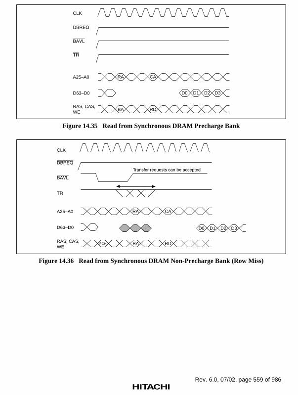
Rev. 6.0, 07/02, page 559 of 986
CLK
A25–A0
D63–D0
RAS, CAS,WE
D0
RA CA
D1 D2 D3
BA RD
Figure 14.35 Read from Synchronous DRAM Precharge Bank
CLK
A25–A0
D63–D0
RAS, CAS,WE
RA CA
D0 D1 D2 D3
PCH BA RD
Transfer requests can be accepted
Figure 14.36 Read from Synchronous DRAM Non-Precharge Bank (Row Miss)
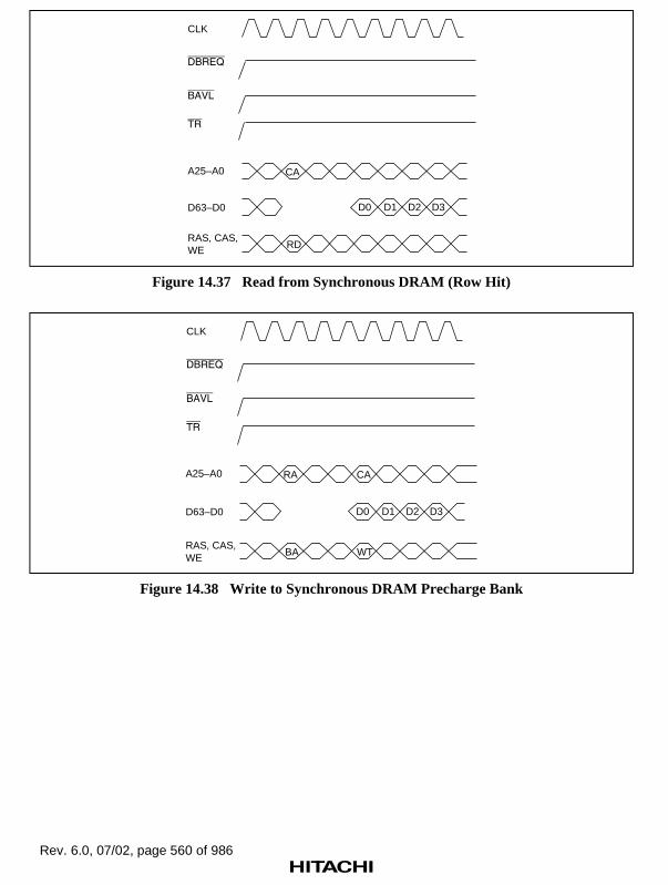
Rev. 6.0, 07/02, page 560 of 986
CLK
A25–A0
D63–D0
RAS, CAS,WE
CA
RD
D0 D1 D2 D3
Figure 14.37 Read from Synchronous DRAM (Row Hit)
CLK
A25–A0
D63–D0
RAS, CAS,WE
RA CA
BA WT
D0 D1 D2 D3
Figure 14.38 Write to Synchronous DRAM Precharge Bank

Rev. 6.0, 07/02, page 561 of 986
CLK
A25–A0
D63–D0
RAS, CAS,WE
RA CA
D0 D1 D2 D3
PCH BA WT
Transfer requests can be accepted
Figure 14.39 Write to Synchronous DRAM Non-Precharge Bank (Row Miss)
CLK
A25–A0
D63–D0
RAS, CAS,WE
D0
CA
D1 D2 D3
WT
Figure 14.40 Write to Synchronous DRAM (Row Hit)

Rev. 6.0, 07/02, page 562 of 986
00
D0 D1 D2
RA CA
RDBA
DTR
CLK
ID1, ID0
RAS,CAS, WE
D63–D0
A25–A0
Figure 14.41 Single Address Mode/Burst Mode/External Bus →→→→ External Device 32-ByteBlock Transfer/Channel 0 On-Demand Data Transfer

Rev. 6.0, 07/02, page 563 of 986
DMA Operation Register (DMAOR)
31 15 9 8 2 1 0
DDT
PR[1:0] AENMIF
DMECOD(SH7750S)
4
DDT: 0: Normal DMA mode1: On-demand data transfer mode
Figure 14.42 DDT Mode Setting
DTRMD = 01
CA CA
D0 D1 D2 D3 D0 D1 D2 D3 D1 D2 D3
WTWT
CLK
ID1, ID0
CMD
D63–D0
A25–A0
Start of data transfer
No DMA request sampling
Figure 14.43 Single Address Mode/Burst Mode/Edge Detection/External Device →→→→ External Bus Data Transfer

Rev. 6.0, 07/02, page 564 of 986
CA CA
D0 D1 D2 D3 D0 D1 D2 D3DTRMD = 10
RD RD
Start of data transfer
Wait for next DMA request
CLK
ID1, ID0
CMD
D63–D0
A25–A0
Figure 14.44 Single Address Mode/Burst Mode/Level Detection/External Bus →→→→ External Device Data Transfer
CA CACA
RD RDRD
DTR D0 D3D2
CLK
ID1, ID0
DQMn
D63–D0
A25–A0
CMD
Idle cycle Idle cycle Idle cycleMD = 01
Figure 14.45 Single Address Mode/Burst Mode/Edge Detection/Byte, Word, Longword,Quadword/External Bus →→→→ External Device Data Transfer

Rev. 6.0, 07/02, page 565 of 986
CA CACA
WT
DTR D0 D3D1
CLK
ID1, ID0
DQMn
D63–D0
A25–A0
CMD
Idle cycle
MD = 01
Idle cycle Idle cycle
WT WT
Figure 14.46 Single Address Mode/Burst Mode/Edge Detection/Byte, Word, Longword,Quadword/External Device →→→→ External Bus Data Transfer

Rev. 6.0, 07/02, page 566 of 986
DTR
ID = 1, 2, or 3
RA CA
BA RD
D0 D1 D2 D3
CLK
ID1, ID0
RAS,CAS, WE
D63–D0
A25–A0
01 or 10 or 11
Figure 14.47 Single Address Mode/Burst Mode/32-Byte Block Transfer/DMA TransferRequest to Channels 1–3 Using Data Bus

Rev. 6.0, 07/02, page 567 of 986
RA CA
BA RD
10
D0 D1 D2 D3 D4 D5 D6 D7
CLK
ID1, ID0
RAS,CAS, WE
D63–D0
A25–A0
No DTR cycle, so requests can be made at any time
Figure 14.48 Single Address Mode/Burst Mode/32-Byte Block Transfer/External Bus →→→→ External Device Data Transfer/
Direct Data Transfer Request to Channel 2 without Using Data Bus

Rev. 6.0, 07/02, page 568 of 986
CLK
ID1, ID0
D63–D0
A25–A0
RAS, CAS, WE
3rd 4th 5th
Four requests can be queued Handshaking is necessary to send additional requests
Must be ignored (no request transmitted)
CA CARA
BA RD NOPRD
CA
D1 D2 D3 D0 D1 D2 D3 D1 D2
RD
D0D0
No more requests
2nd1st
Figure 14.49 Single Address Mode/Burst Mode/External Bus →→→→ External Device DataTransfer/Direct Data Transfer Request to Channel 2

Rev. 6.0, 07/02, page 569 of 986
CLK
ID1, ID0
D63–D0
A25–A0
RAS,CAS, WE
3rd 4th 5th
Four requests can be queued Handshaking is necessary to send additional requests
CA CARA CA CA
D0 D1 D2 D3 D0 D1 D2 D3 D0 D1 D2 D3
BA WTWT WT WT
Must be ignored (no request transmitted)
2nd1st
Figure 14.50 Single Address Mode/Burst Mode/External Device →→→→ External Bus DataTransfer/Direct Data Transfer Request to Channel 2
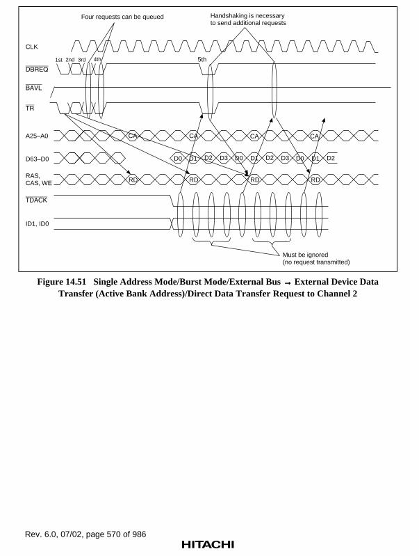
Rev. 6.0, 07/02, page 570 of 986
CLK
ID1, ID0
D63–D0
A25–A0
RAS,CAS, WE
3rd 4th 5th
CA CA CACA
D0 D1 D2 D3 D0 D1 D2 D3 D0 D1 D2
RD RDRDRD
Four requests can be queued Handshaking is necessary to send additional requests
Must be ignored (no request transmitted)
2nd1st
Figure 14.51 Single Address Mode/Burst Mode/External Bus →→→→ External Device DataTransfer (Active Bank Address)/Direct Data Transfer Request to Channel 2

Rev. 6.0, 07/02, page 571 of 986
CLK
ID1, ID0
D63–D0
A25–A0
RAS,CAS, WE
3rd 4th 5th
CA CA CA CA
D0 D1 D2 D3 D0 D1 D2 D3 D0 D1 D2 D3
WTWT WT WT
Four requests can be queued Handshaking is necessary to send additional requests
Must be ignored (no request transmitted)
2nd1st
Figure 14.52 Single Address Mode/Burst Mode/External Device →→→→ External Bus DataTransfer (Active Bank Address)/Direct Data Transfer Request to Channel 2
14.5.4 Notes on Use of DDT Module
1. Normal data transfer mode (channel 0)
Initial settings for channel 0 demand transfer must be DTR.ID = 00 and DTR.MD = 01, 10, or11. In this case, only single address mode can be set for channel 0.
2. Normal data transfer mode (channels 1 to 3)
If a setting of DTR.ID = 01, 10, or 11 is made, DTR.MD will be ignored.
3. Handshake protocol using the data bus (valid on channel 0 only)
a. The handshake protocol using the data bus can be executed only on channel 0. (SetDTR.ID = 00, DTR.MD = 00, DTR.SZ ≠ 101 or 110. Operation is not guaranteed ifsettings of DTR.ID = 00, DTR.MD = 00, and DTR.SZ = 101 or 110 are made.)
b. If, during execution of the handshake protocol using the data bus for channel 0, a request isinput for one of channels 1 to 3, and after that DMA transfer is executed settings ofDTR.ID = 00, DTR.MD = 00, and DTR, SZ ≠ 101.110 are input in the handshake protocolusing the data bus, a transfer request will be asserted for channel 0.

Rev. 6.0, 07/02, page 572 of 986
c. In the SH7750S and SH7750R, initial settings can be made in the DMAC channel 0 controlregister from the CPU (possible settings are CHCR0.RS = 0000, 0010, or 0011). If settingsof DTR.ID = 00, DTR.MD = 00, and DTR.SZ ≠ 101 or 110 are subsequently input, atransfer request to channel 0 will be asserted.
4. Handshake protocol without use of the data bus
a. With the handshake protocol without use of the data bus, a DMA transfer request can beinput to the DMAC again for the channel for which transfer was requested immediatelybefore by asserting TR only.
b. When using the handshake protocol without use of the data bus, first make the necessarysettings in the DMAC control registers.
c. When not using the handshake protocol without use of the data bus, if TR only is assertedwithout outputting DTR, a request will be issued for the channel for which DMA transferwas requested immediately before. Also, if the first DMA transfer request after a power-onreset is input by asserting TR only, it will be ignored and the DMAC will not operate.
d. If TR only is asserted by means of the handshake protocol without use of the data bus and aDMA transfer request is input when channel 0 DMA transfer has ended and CHCR0.TE =1, the DMAC will freeze. Before issuing a DMA transfer request, the TE flag must becleared by writing CHCR0.TE = 0 after reading CHCR0.TE = 1.
5. Direct data transfer mode (valid on channel 2 only)
a. If a DMA transfer request for channel 2 is input by simultaneous assertion of DBREQ andTR during DMA transfer execution with the handshake protocol without use of the databus, it will be accepted if there is space in the DDT channel 2 request queue.
b. In direct data transfer mode (with DBREQ and TR asserted simultaneously), DBREQ is notinterpreted as a bus arbitration signal, and therefore the BAVL signal is never asserted.
6. Request queue transfer request acceptance
a. The DDT has four request queues for each of channels 1 to 3. When these request queuesare full, a DMA transfer request from an external device will be ignored.
b. If a DMA transfer request for channel 0 is input during execution of a channel 0 DMA buscycle, the DDT will ignore that request. Confirm that channel 0 DMA transfer has finished(burst mode) or that a DMA bus cycle is not in progress (cycle steal mode).
7. DTR format
a. The DDT module processes DTR.ID, DTR.MD, and DTR.SZ as follows.
When DTR.ID= 00
• MD = 00, SZ ≠ 101, 110: Handshake protocol using the data bus
• MD ≠ 00, SZ = 111: CHCR0.DE = 0 setting (DMA transfer end request)
• MD ≠ 10, SZ = 110: DDT request queue clear
When DTR.ID ≠ 00
• Transfer request to channels 1—3 (items other than ID ignored)

Rev. 6.0, 07/02, page 573 of 986
8. Data transfer end request
a. A data transfer end request (DTR.ID = 00, MD ≠ 00, SZ = 111) cannot be accepted duringchannel 0 DMA transfer. Therefore, if edge detection and burst mode are set for channel 0,transfer cannot be ended midway.
b. When a transfer end request (DTR.ID = 00, MD ≠ 00, SZ = 111) is accepted, the values setin CHCR0, SAR0, DAR0, and DMATCR0 are retained. With the SH7750, executioncannot be restarted from an external device in this case. To restart execution in theSH7750S and SH7750R, set CHCR0.DE = 1 with an MOV instruction.
9. Request queue clearance
a. When settings of DTR.ID = 00, DTR.MD = 10, and SZ = 110 are accepted by the DDT innormal data transfer mode, DDT channel 0 requests and channel 1 to 3 request queues areall cleared. All external requests held on the DMAC side are also cleared.
b. In case 4-d, the DMAC freeze state can be cleared.
c. When settings of DMAOR.DDT = 1, DTR.ID = 00, DTR.MD = 10, and SZ = 110 areaccepted by the DDT in case 11, the DMAC freeze state can be cleared.
10. DBREQ assertion
a. After DBREQ is asserted, do not assert DBREQ again until BAVL is asserted, as this willresult in a discrepancy between the number of DBREQ and BAVL assertions.
b. The BAVL assertion period due to DBREQ assertion is one cycle.
If a row address miss occurs in a read or write in the non-precharged bank duringsynchronous DRAM access, BAVL is asserted for a number of cycles in accordance withthe RAS precharge interval set in BSC.MCR.TCP.
c. It takes one cycle for DBREQ to be accepted by the DMAC after being asserted by anexternal device. If a row address miss occurs at this time in a read or write in the non-precharged bank during synchronous DRAM access, and BAVL is asserted, the DBREQsignal asserted by the external device is ignored. Therefore, BAVL is not asserted againdue to this signal.
11. Clearing DDT mode
Check that DMA transfer is not in progress on any channel before setting the DMAOR.DDTbit. If the DMAOR.DDT setting is changed from 1 to 0 during DMA transfer in DDT mode,the DMAC will freeze.
This also applies when switching from normal DMA mode (DMAOR.DDT = 0) to DDTmode.
12. Confirming DMA transfer requests and number of transfers executed
The channel associated with a DMA bus cycle being executed in response to a DMA transferrequest can be confirmed by determining the level of external pins ID1 and ID0 at the risingedge of the CKIO clock while TDACK is asserted.
(ID = 00: channel 0; ID = 01: channel 1; ID = 10: channel 2; ID = 11: channel 3)

Rev. 6.0, 07/02, page 574 of 986
14.6 Configuration of the DMAC (SH7750R)
14.6.1 Block Diagram of the DMAC
Figure 14.53 is a block diagram of the DMAC in the SH7750R.
Request
8
dmaqueclr0-7
queclr0–7
SAR0, DAR0, DMATCR0,CHCR0 only
DDTMODEBAVL
48 bits
CH0 CH1 CH2 CH3
CH4 CH5 CH6 CH7
Request controller
DTR command buffer
DDT module
DDTDExternal bus
tdack
id[2:0]
ID[1:0]
D[63:0]
DBREQ/
SARn
DARn
DMATCRn
CHCRn
DMAOR
Businterface
Per
iphe
ral b
us
Inte
rnal
bus
DMAC module
Count control
Registr control
Activationcontrol
Requestprioritycontrol
32B databuffer
Bus statecontroller
On-chipperipheral
module
Ext
erna
l add
ress
/on-
chip
perip
hera
l mod
ule
addr
ess
TMUSCI, SCIF
DACK0, DACK1DRAK0, DRAK1
,
DMAORn:SARn:DARn:DMATCRn:CHCRn:
n = 0 to 7
DMAC operation registerDMAC source address registerDMAC destination address registerDMAC transfer count registerDMAC channel control register
Figure 14.53 Block Diagram of the DMAC

Rev. 6.0, 07/02, page 575 of 986
14.6.2 Pin Configuration (SH7750R)
Tables 14.11 and 14.12 show the pin configuration of the DMAC.
Table 14.11 DMAC Pins
Channel Pin Name Abbreviation I/O Function
0 DMA transferrequest
DREQ0 Input DMA transfer request input fromexternal device to channel 0
DREQ acceptanceconfirmation
DRAK0 Output Acceptance of request for DMAtransfer from channel 0 to externaldevice
Notification to external device of startof execution
DMA transfer endnotification
DACK0 Output Strobe output to external device ofDMA transfer request from channel 0to external device
1 DMA transferrequest
DREQ1 Input DMA transfer request input fromexternal device to channel 1
DREQ acceptanceconfirmation
DRAK1 Output Acceptance of request for DMAtransfer from channel 1 to externaldevice
Notification to external device of startof execution
DMA transfer endnotification
DACK1 Output Strobe output to external device ofDMA transfer request from channel 1to external device

Rev. 6.0, 07/02, page 576 of 986
Table 14.12 DMAC Pins in DDT Mode
Pin Name Abbreviation I/O Function
Data bus request DBREQ(DREQ0)
Input Data bus release request from externaldevice for DTR format input
Data bus available BAVL/ID2(DRAK0)
Output Data bus release notification
Data bus can be used 2 cycles afterBAVL is asserted
Notification of channel number toexternal device at same time as TDACKoutput
Transfer request signal TR(DREQ1)
Input If asserted 2 cycles after BAVLassertion, DTR format is sent
Only TR asserted: DMA request
DBREQ and TR assertedsimultaneously: Direct request tochannel 2
DMAC strobe TDACK(DACK0)
Output Reply strobe signal for external devicefrom DMAC
Channel numbernotification
ID[1:0](DRAK1, DACK1)
Output Notification of channel number toexternal device at same time as TDACKoutput
(ID [1] = DRAK1, ID [0] = DACK1)
Requests for DMA transfer from external devices are normally accepted only on channel 0(DREQ0) and channel 1 (DREQ1). In DDT mode, the BAVL pin functions as both the data-bus-available pin and channel-number-notification (ID2) pin.
14.6.3 Register Configuration (SH7750R)
Table 14.13 shows the configuration of the DMAC’s registers. The DMAC of the SH7750R has atotal of 33 registers: four registers are assigned to each channel, and there is a control register forthe overall control of the DMAC.
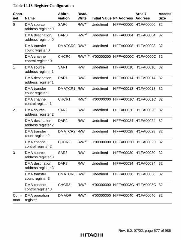
Rev. 6.0, 07/02, page 577 of 986
Table 14.13 Register Configuration
Chan-nel Name
Abbre-viation
Read/Write Initial Value P4 Address
Area 7Address
AccessSize
DMA sourceaddress register 0
SAR0 R/W*2 Undefined H'FFA00000 H'1FA00000 32
DMA destinationaddress register 0
DAR0 R/W*2 Undefined H'FFA00004 H'1FA00004 32
DMA transfercount register 0
DMATCR0 R/W*2 Undefined H'FFA00008 H'1FA00008 32
0
DMA channelcontrol register 0
CHCR0 R/W*1*2 H'00000000 H'FFA0000C H'1FA0000C 32
DMA sourceaddress register 1
SAR1 R/W Undefined H'FFA00010 H'1FA00010 32
DMA destinationaddress register 1
DAR1 R/W Undefined H'FFA00014 H'1FA00014 32
DMA transfercount register 1
DMATCR1 R/W Undefined H'FFA00018 H'1FA00018 32
1
DMA channelcontrol register 1
CHCR1 R/W*1 H'00000000 H'FFA0001C H'1FA0001C 32
DMA sourceaddress register 2
SAR2 R/W Undefined H'FFA00020 H'1FA00020 32
DMA destinationaddress register 2
DAR2 R/W Undefined H'FFA00024 H'1FA00024 32
DMA transfercount register 2
DMATCR2 R/W Undefined H'FFA00028 H'1FA00028 32
2
DMA channelcontrol register 2
CHCR2 R/W*1 H'00000000 H'FFA0002C H'1FA0002C 32
DMA sourceaddress register 3
SAR3 R/W Undefined H'FFA00030 H'1FA00030 32
DMA destinationaddress register 3
DAR3 R/W Undefined H'FFA00034 H'1FA00034 32
DMA transfercount register 3
DMATCR3 R/W Undefined H'FFA00038 H'1FA00038 32
3
DMA channelcontrol register 3
CHCR3 R/W*1 H'00000000 H'FFA0003C H'1FA0003C 32
Com-mon
DMA operationregister
DMAOR R/W*1 H'00000000 H'FFA00040 H'1FA00040 32

Rev. 6.0, 07/02, page 578 of 986
Table 14.13 Register Configuration (cont)
Chan-nel Name
Abbre-viation
Read/Write Initial Value P4 Address
Area 7Address
AccessSize
DMA sourceaddress register 4
SAR4 R/W Undefined H'FFA00050 H'1FA00050 32
DMA destinationaddress register 4
DAR4 R/W Undefined H'FFA00054 H'1FA00054 32
DMA transfercount register 4
DMATCR4 R/W Undefined H'FFA00058 H'1FA00058 32
4
DMA channelcontrol register 4
CHCR4 R/W*1 H'00000000 H'FFA0005C H'1FA0005C 32
DMA sourceaddress register 5
SAR5 R/W Undefined H'FFA00060 H'1FA00060 32
DMA destinationaddress register 5
DAR5 R/W Undefined H'FFA00064 H'1FA00064 32
DMA transfercount register 5
DMATCR5 R/W Undefined H'FFA00068 H'1FA00068 32
5
DMA channelcontrol register 5
CHCR5 R/W*1 H'00000000 H'FFA0006C H'1FA0006C 32
DMA sourceaddress register 6
SAR6 R/W Undefined H'FFA00070 H'1FA00070 32
DMA destinationaddress register 6
DAR6 R/W Undefined H'FFA00074 H'1FA00074 32
DMA transfercount register 6
DMATCR6 R/W Undefined H'FFA00078 H'1FA00078 32
6
DMA channelcontrol register 6
CHCR6 R/W*1 H'00000000 H'FFA0007C H'1FA0007C 32
DMA sourceaddress register 7
SAR7 R/W Undefined H'FFA00080 H'1FA00080 32
DMA destinationaddress register 7
DAR7 R/W Undefined H'FFA00084 H'1FA00084 32
DMA transfercount register 7
DMATCR7 R/W Undefined H'FFA00088 H'1FA00088 32
7
DMA channelcontrol register 7
CHCR7 R/W*1 H'00000000 H'FFA0008C H'1FA0008C 32
Notes: Longword access should be used for all control registers. If a different access width isused, reads will return all 0s and writes will not be possible.
*1 Bit 1 of CHCR0–CHCR7 and bits 2 and 1 of DMAOR can only be written with 0 afterbeing read as 1, to clear the flags.
*2 In the SH7750R, writes from the CPU and writes from external I/O devices using theDTR format are possible in DDT mode.

Rev. 6.0, 07/02, page 579 of 986
14.7 Register Descriptions (SH7750R)
14.7.1 DMA Source Address Registers 0–7 (SAR0–SAR7)
Bit: 31 30 29 28 27 26 25 24 23 22 21 20 19 18 17 16
Initial value: — — — — — — — — — — — — — — — —
R/W: R/W R/W R/W R/W R/W R/W R/W R/W R/W R/W R/W R/W R/W R/W R/W R/W
Bit: 15 14 13 12 11 10 9 8 7 6 5 4 3 2 1 0
Initial value: — — — — — — — — — — — — — — — —
R/W: R/W R/W R/W R/W R/W R/W R/W R/W R/W R/W R/W R/W R/W R/W R/W R/W
DMA source address registers 0–7 (SAR0–SAR7) are 32-bit readable/writable registers thatspecify the source address for a DMA transfer. The functions of these registers are the same as onthe SH7750 or SH7750S. For more information, see section 14.2.1, DMA Source AddressRegisters 0–3 (SAR0–SAR3).
14.7.2 DMA Destination Address Registers 0–7 (DAR0–DAR7)
Bit: 31 30 29 28 27 26 25 24 23 22 21 20 19 18 17 16
Initial value: — — — — — — — — — — — — — — — —
R/W: R/W R/W R/W R/W R/W R/W R/W R/W R/W R/W R/W R/W R/W R/W R/W R/W
Bit: 15 14 13 12 11 10 9 8 7 6 5 4 3 2 1 0
Initial value: — — — — — — — — — — — — — — — —
R/W: R/W R/W R/W R/W R/W R/W R/W R/W R/W R/W R/W R/W R/W R/W R/W R/W
DMA destination address registers 0–7 (DAR0–DAR7) are 32-bit readable/writable registers thatspecify the destination address for a DMA transfer. The functions of these registers are the sameas on the SH7750 and SH7750S. For more information, see section 14.2.2, DMA DestinationAddress Registers 0–3 (DAR0–DAR3).

Rev. 6.0, 07/02, page 580 of 986
14.7.3 DMA Transfer Count Registers 0–7 (DMATCR0–DMATCR7)
Bit: 31 30 29 28 27 26 25 24 23 22 21 20 19 18 17 16
Initial value: 0 0 0 0 0 0 0 0 — — — — — — — —
R/W: R R R R R R R R R/W R/W R/W R/W R/W R/W R/W R/W
Bit: 15 14 13 12 11 10 9 8 7 6 5 4 3 2 1 0
Initial value: — — — — — — — — — — — — — — — —
R/W: R/W R/W R/W R/W R/W R/W R/W R/W R/W R/W R/W R/W R/W R/W R/W R/W
DMA transfer count registers 0–7 (DMATCR0–DMATCR7) are 32-bit readable/writable registersthat specify the number of transfers in transfer operations for the corresponding channel (bytecount, word count, longword count, quadword count, or 32-byte count). Functions of theseregisters are the same as the transfer-count registers of the SH7750 or SH7750S. For moreinformation, see section 14.2.3, DMA Transfer Count Registers 0–3 (DMATCR0–DMATCR3).
14.7.4 DMA Channel Control Registers 0–7 (CHCR0–CHCR7)
Bit: 31 30 29 28 27 26 25 24 23 22 21 20 19 18 17 16
SSA2 SSA1 SSA0 STC DSA2 DSA1 DSA0 DTC — — — — DS RL AM AL
Initial value: 0 0 0 0 0 0 0 0 0 0 0 0 0 0 0 0
R/W: R/W R/W R/W R/W R/W R/W R/W R/W R R R R R/W (R/W) R/W (R/W)
Bit: 15 14 13 12 11 10 9 8 7 6 5 4 3 2 1 0
DM1 DM0 SM1 SM0 RS3 RS2 RS1 RS0 TM TS2 TS1 TS0 QCL IE TE DE
Initial value: 0 0 0 0 0 0 0 0 0 0 0 0 0 0 0 0
R/W: R/W R/W R/W R/W R/W R/W R/W R/W R/W R/W R/W R/W R/(W) R/W R/(W) R/W
DMA channel control registers 0–7(CHCR0–CHCR7) are 32-bit readable/writable registers thatspecify the operating mode, transfer method, etc., for each channel. Bits 31–28 and 27–24correspond to the source address and destination address, respectively; these settings are onlyvalid when the transfer involves the CS5 or CS6 space and the relevant space has been specified asa PCMCIA-interface space. In other cases, these bits should be cleared to 0. For more informationabout the PCMCIA interface, see section 13.3.7, PCMCIA Interface, in section 13, Bus StateController.

Rev. 6.0, 07/02, page 581 of 986
No function is assigned to bits 18 and 16 of the CHCR2–CHCR7 registers. Writing to these bits ofthe CHCR2–CHCR7 registers is invalid. If, however, a value is written to these bits, it shouldalways be 0. These bits are always read as 0.
These registers are initialized to H'00000000 by a power-on or manual reset. Their values areretained in standby, sleep, and deep-sleep modes.
Bits 31 to 29—Source Address Space Attribute Specification (SSA2–SSA0): These bits specifythe space attribute for PCMCIA access. These bits are only valid in the case of page mapping toPCMCIA connected to areas 5 and 6. For details of the settings, see the description of the SSA2-SSA0 bits in section 14.2.4, DMA Channel Control Registers 0–3 (CHCR0–CHCR3).
Bit 28—Source Address Wait Control Select (STC): Specifies CS5 or CS6 space wait controlfor PCMCIA access. This bit selects the wait control register in the BSC that performs area 5 and6 wait cycle control. For details of the settings, see the description of the STC bit in section 14.2.4,DMA Channel Control Registers 0–3 (CHCR0–CHCR3).
Bits 27 to 25—Destination Address Space Attribute Specification (DSA2–DSA0): These bitsspecify the space attribute for PCMCIA access. These bits are only valid in the case of pagemapping to PCMCIA connected to areas 5 and 6. For details of the settings, see the description ofthe DSA2–DSA0 bits in section 14.2.4, DMA Channel Control Registers 0–3 (CHCR0–CHCR3).
Bit 24—Destination Address Wait Control Select (DTC): Specifies CS5 or CS6 space waitcycle control for PCMCIA access. This bit selects the wait control register in the BSC thatperforms area 5 and 6 wait cycle control. For details of the settings, see the description of the DTCbit in section 14.2.4, DMA Channel Control Registers 0–3 (CHCR0–CHCR3).
Bits 23 to 20—Reserved: These bits are always read as 0, and should only be written with 0.
Bit 19—DREQDREQDREQDREQ Select (DS): Specifies either low level detection or falling edge detection as thesampling method for the DREQ pin used in external request mode.
In normal DMA mode, this bit is valid only in CHCR0 and CHCR1. In DDT mode, it is valid inCHCR0–CHCR7. For details of the settings, see the description of the DS bit in section 14.2.4,DMA Channel Control Registers 0–3 (CHCR0–CHCR3).
Bit 18—Request Check Level (RL): Selects whether the DRAK signal (that notifies an externaldevice of the acceptance of DREQ) is an active-high or active-low output.
This bit is valid only in CHCR0 and CHCR1 in normal mode, and is invalid in DDT mode. Fordetails of the settings, see the description of the RL bit in section 14.2.4, DMA Channel ControlRegisters 0–3 (CHCR0–CHCR3).

Rev. 6.0, 07/02, page 582 of 986
Bit 17—Acknowledge Mode (AM): In dual address mode, selects whether DACK is output in thedata read cycle or write cycle. In single address mode, DACK is always output regardless of thesetting of this bit.
In normal DMA mode, this bit is valid only in CHCR0 and CHCR1. In DDT mode, it is valid inCHCR0–CHCR7. (DDT mode: TDACK) For details of the settings, see the description of the AMbit in section 14.2.4, DMA Channel Control Registers 0–3 (CHCR0–CHCR3).
Bit 16—Acknowledge Level (AL): Specifies the DACK (acknowledge) signal as active-high oractive-low.
This bit is valid only in CHCR0 and CHCR1 in normal mode, and is invalid in DDT mode. Fordetails of the settings, see the description of the AL bit in section 14.2.4, DMA Channel ControlRegisters 0–3 (CHCR0–CHCR3).
Bits 15 and 14—Destination Address Mode 1 and 0 (DM1, DM0): These bits specifyincrementing/decrementing of the DMA transfer destination address. The specification of thesebits is ignored when data is transferred from external memory to an external device in singleaddress mode. For details of the settings, see the description of the DM1 and DM0 bits in section14.2.4, DMA Channel Control Registers 0–3 (CHCR0–CHCR3).
Bits 13 and 12—Source Address Mode 1 and 0 (SM1, SM0): These bits specifyincrementing/decrementing of the DMA transfer source address. The specification of these bits isignored when data is transferred from an external device to external memory in single addressmode. For details of the settings, see the description of the SM1 and SM0 bits in section 14.2.4,DMA Channel Control Registers 0–3 (CHCR0–CHCR3).
Bits 11 to 8—Resource Select 3 to 0 (RS3–RS0): These bits specify the transfer request source.For details of the settings, see the description of the RS3–RS0 bits in section 14.2.4, DMAChannel Control Registers 0–3 (CHCR0–CHCR3).
Bit 7—Transmit Mode (TM): Specifies the bus mode for transfer. For details of the settings, seethe description of the TM bit in section 14.2.4, DMA Channel Control Registers 0–3 (CHCR0–CHCR3).
Bits 6 to 4—Transmit Size 2 to 0 (TS2–TS0): These bits specify the transfer data size (accesssize). For details of the settings, see the description of the TS2–TS0 bits in section 14.2.4, DMAChannel Control Registers 0–3 (CHCR0–CHCR3).
Bit 3 Request Queue Clear (QCL): Writing a 1 to this bit clears the request queues of thecorresponding channel as well as any external requests that have already been accepted. This bit isonly functional when DMAOR.DDT = 1 and DMAOR.DBL = 1.

Rev. 6.0, 07/02, page 583 of 986
CHCR Bit 3
QCL Description
0 This bit is always read as 0. (Initial value)
Writing a 0 to this bit is invalid.
1 When DMAOR.DBL = 1, writing a 1 to this bit clears the request queues on theDDT side and any external requests stored in the DMAC. The written value isnot retained.
Bit 2—Interrupt Enable (IE): When this bit is set to 1, an interrupt request (DMTE) is generatedafter the number of data transfers specified in DMATCR (when TE = 1). For details of thesettings, see the description of the IE bit in section 14.2.4, DMA Channel Control Registers 0–3(CHCR0–CHCR3).
Bit 1—Transfer End (TE): This bit is set to 1 after the number of transfers specified inDMATCR. If the IE bit is set to 1 at this time, an interrupt request (DMTE) is generated.
If data transfer ends before TE is set to 1 (for example, due to an NMI interrupt, address error, orclearing of the DE bit or the DME bit in DMAOR), the TE bit is not set to 1. When this bit is 1,the transfer enabled state is not entered even if the DE bit is set to 1. For details of the settings, seethe description of the TE bit in section 14.2.4, DMA Channel Control Registers 0–3 (CHCR0–CHCR3).
Bit 0—DMAC Enable (DE): Enables operation of the corresponding channel. For details of thesettings, see the description of the DE bit in section 14.2.4, DMA Channel Control Registers 0–3(CHCR0–CHCR3).
14.7.5 DMA Operation Register (DMAOR)
Bit: 31 30 29 28 27 26 25 24 23 22 21 20 19 18 17 16
Initial value: 0 0 0 0 0 0 0 0 0 0 0 0 0 0 0 0
R/W: R R R R R R R R R R R R R R R R
Bit: 15 14 13 12 11 10 9 8 7 6 5 4 3 2 1 0
DDT DBL — — — — PR1 PR0 — — — — — AE NMIF DME
Initial value: 0 0 0 0 0 0 0 0 0 0 0 0 0 0 0 0
R/W: R/W R/W R R R R R/W R/W R R R R R R/(W) R/(W) R/W
DMAOR is a 32-bit readable/writable register that specifies the DMAC transfer mode.

Rev. 6.0, 07/02, page 584 of 986
DMAOR is initialized to H'00000000 by a power-on or manual reset. They retain their values instandby mode and deep sleep mode.
Bits 31 to 16—Reserved: These bits are always read as 0, and should only be written with 0.
Bit 15—On-Demand Data Transfer (DDT): Specifies on-demand data transfer mode. Fordetails of the settings, see the description of the DDT bit in section 14.2.5, DMA OperationRegister (DMAOR)
Bit 14 Number of DDT-Mode Channels (DBL): Selects the number of channels that are ableto accept external requests in DDT mode.
Bit 14: DBL Description
0 Four DDT-mode channels (Initial value)
1 Eight DDT-mode channels
Note: When DMAOR.DBL = 0, channels 4 to 7 cannot accept external requests.
When DMAOR.DBL = 1, one channel can be selected from among channels 0–7 by thecombination of DTR.SZ and DTR.ID in the DTR format (see figure 14.54). Table 14.14 shows thechannel selection by DTR format in the DDT mode.
Table 14.14 Channel Selection by DTR Format (DMAOR.DBL = 1)
DTR.ID[1:0] DTR.SZ[2:0] ≠≠≠≠ 101 DTR.SZ[2:0] = 101
00 CH0 CH4
01 CH1 CH5
10 CH2 CH6
11 CH3 CH7
SZ ID MD COUNT ADDRESSR/W (Reserved)
63 61 60 59 58 57 56 55 4847 32 31 0
Figure 14.54 DTR Format (Transfer Request Format) (SH7750R)
Bits 13 to 10—Reserved: These bits are always read as 0, and should only be written with 0.
Bits 9 and 8—Priority Mode 1 and 0 (PR1, PR0): These bits determine the order of priority forchannel execution when transfer requests are made for a number of channels simultaneously.

Rev. 6.0, 07/02, page 585 of 986
DMAORBit 9
DMAORBit 8
PR1 PR0 Description
0 0 CH0 > CH1 > CH2 > CH3 > CH4 > CH5 > CH6 > CH7 (Initial value)
0 1 CH0 > CH2 > CH3 > CH4 > CH5 > CH6 > CH7 > CH1
1 0 CH2 > CH0 > CH1 > CH3 > CH4 > CH5 > CH6 > CH7
1 1 Round robin mode
Bits 7 to 3—Reserved: These bits are always read as 0, and should only be written with 0.
Bit 2—Address Error Flag (AE): Indicates that an address error has occurred during DMAtransfer. If this bit is set during data transfer, transfers on all channels are suspended, and aninterrupt request (DMAE) is generated. The CPU cannot write 1 to AE. This bit can only becleared by writing 0 after reading 1. For details of the settings, see the description of the AE bit insection 14.2.5, DMA Operation Register (DMAOR)
Bit 1—NMI Flag (NMIF): Indicates that NMI has been input. This bit is set regardless ofwhether or not the DMAC is operating. If this bit is set during data transfer, transfers on allchannels are suspended. The CPU cannot write 1 to NMIF. This bit can only be cleared by writing0 after reading 1. For details of the settings, see the description of the NMIF bit in section 14.2.5,DMA Operation Register (DMAOR)
Bit 0—DMAC Master Enable (DME): Enables activation of the entire DMAC. When the DMEbit and the DE bit of the CHCR register for the corresponding channel are set to 1, that channel isenabled for transfer. If this bit is cleared during data transfer, transfers on all channels aresuspended.
Even if the DME bit has been set, transfer is not enabled when TE is 1 or DE is 0 in CHCR, orwhen the NMI or AE bit in DMAOR is 1. For details of the settings, see the description of theDME bit in section 14.2.5, DMA Operation Register (DMAOR)

Rev. 6.0, 07/02, page 586 of 986
14.8 Operation (SH7750R)
Operation specific to the SH7750R is described here. For details of operation, see section 14.3,Operation.
14.8.1 Channel Specification for a Normal DMA Transfer
In normal DMA transfer mode, the DMAC always operates with eight channels, and externalrequests are only accepted on channel 0 (DREQ) and channel 1 (DREQ1).
After setting the registers of the channels in use, including CHCR, SAR, DAR, and DMATCR,DMA transfer is started on receiving a DMA transfer request in the transfer-enabled state (DE = 1,DME = 1, TE = 0, NMIF = 0, AE = 0), in the order of predetermined priority. The transfer endswhen the transfer-end condition is satisfied. There are three modes for transfer requests: auto-request, external request, and on-chip peripheral module request. The addressing modes for DMAtransfer are the single-address mode and the dual-address mode. Bus mode is selectable betweenburst mode and cycle steal mode.
14.8.2 Channel Specification for DDT-Mode DMA Transfer
For DMA transfer in DDT mode, the DMAOR.DBL setting selects either four or eight channels.External requests are accepted on channels 0–3 when DMAOR.DBL = 0, and on channels 0–7when DMAOR.DBL = 1. For further information on these settings, see the entry on the DBL bit insection 14.7.5, DMA Operation Register (DMAOR).
14.8.3 Transfer Channel Notification in DDT Mode
When the DMAC is set up for four-channel external request acceptance in DDT mode(DMAOR.DBL = 0), the ID [1:0] bits are used to notify the external device of the DMAC channelthat is to be used. For more details, see section 14.5, On-Demand Data Transfer Mode.
When the DMAC is set up for eight-channel external request acceptance in DDT mode(DMAOR.DBL = 1), the ID [1:0] bits and the simultaneous (on the timing of TDACK assertion)assertion of ID2 from the BAVL (bus-release notification) pin are used to notify the externaldevice of the DMAC channel that is to be used (see table 14.15, Notification of Transfer Channelin Eight-Channel DDT Mode).
When the DMAC is set up for eight-channel external request acceptance in DDT mode(DMAOR.DBL = 1), it is important to note that the BAVL pin has the two functions as shown intable 14.16.

Rev. 6.0, 07/02, page 587 of 986
Table 14.15 Notification of Transfer Channel in Eight-Channel DDT Mode
BAVLBAVLBAVLBAVL/ID2ID2ID2ID2 ID[1:0] Transfer Channel
00 CH0
01 CH1
10 CH2
1
11 CH3
00 CH4
01 CH5
10 CH6
0
11 CH7
Table 14.16 Function of BAVLBAVLBAVLBAVL
Function of BAVLBAVLBAVLBAVL
TDACK = High Bus available (data-bus enabled)
TDACK = Low Notification of channel number (ID2)
14.8.4 Clearing Request Queues by DTR Format
In DDT mode, the request queues of any channel can be cleared by using DTR.ID, DTR.MD,DTR.SZ, and DTR.COUNT [7:4] in a DTR format. This function is only available whenDMAOR.DBL = 1. Table 14.17 shows the DTR format settings for clearing request queues.

Rev. 6.0, 07/02, page 588 of 986
Table 14.17 DTR Format for Clearing Request Queues
DMAOR.DBL DTR.ID DTR.MD DTR.SZ DTR.COUNT[7:4] Description
10 Clear the request queues of all channels(1–7).
Clear the CH0 request-accepted flag
0 00
11
110 *
Setting prohibited
10 * Clear the request queues of all channels(1–7).
Clear the CH0 request-accepted flag.
0001 Clear the CH0 request-accepted flag
0010 Clear the CH1 request queues.
0011 Clear the CH2 request queues.
0100 Clear the CH3 request queues.
0101 Clear the CH4 request queues.
0110 Clear the CH5 request queues.
0111 Clear the CH6 request queues.
1 00
11
110
1000 Clear the CH7 request queues.
Note: (SH7750R) DTR.SZ = DTR[63:61], DTR.ID = DTR[59:58], DTR.MD = DTR[57:56],DTR.COUNT[7:4] = DTR[55:52]
14.8.5 Interrupt-Request Codes
When the number of transfers specified in DMATCR has been finished and the interrupt request isenabled (CHCR.IE = 1), a transfer-end interrupt request can be sent to the CPU from eachchannel. Table 14.18 lists the interrupt-request codes that are associated with these transfer-endinterrupts.

Rev. 6.0, 07/02, page 589 of 986
Table 14.18 DMAC Interrupt-Request Codes
Source of the Interrupt Description INTEVT Code Priority
DMTE0 CH0 transfer-end interrupt H'640 High
DMTE1 CH1 transfer-end interrupt H'660
DMTE2 CH2 transfer-end interrupt H'680
DMTE3 CH3 transfer-end interrupt H'6A0
DMTE4 CH4 transfer-end interrupt H'780
DMTE5 CH5 transfer-end interrupt H'7A0
DMTE6 CH6 transfer-end interrupt H'7C0
DMTE7 CH7 transfer-end interrupt H'7E0
DMAE Address error interrupt H'6C0 Low
DMTE4–DMTE7: These codes are not used in the SH7750 or SH7750S.
CKIO
RA
DTR
CA
D1 D2
RDBA
00ID1, ID0
RAS,CAS, WE
D63–D0
A25–A0
/
D0
Figure 14.55 Single Address Mode/Burst Mode/External Bus →→→→ External Device 32-ByteBlock Transfer/Channel 0 On-Demand Data Transfer
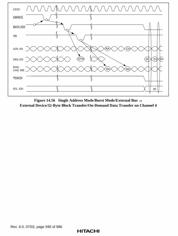
Rev. 6.0, 07/02, page 590 of 986
CKIO
RA
DTR
CA
D1 D2
RDBA
00ID1, ID0
RAS,CAS, WE
D63–D0
A25–A0
/
D0
Figure 14.56 Single Address Mode/Burst Mode/External Bus →→→→External Device/32-Byte Block Transfer/On-Demand Data Transfer on Channel 4

Rev. 6.0, 07/02, page 591 of 986
14.9 Usage Notes
1. When modifying SAR0–SAR3, DAR0–DAR3, DMATCR0–DMATCR3, and CHCR0–CHCR3 in the SH7750 or SH7750S or when modifying SAR0–SAR7, DAR0–DAR7,DMATCR0–DMATCR7, and CHCR0–CHCR7 in the SH7750R, first clear the DE bit for therelevant channel.
2. The NMIF bit in DMAOR is set when an NMI interrupt is input even if the DMAC is notoperating.
Confirmation method when DMA transfer is not executed correctly:
With the SH7750 and SH7750S, read the NMIF, AE, and DME bits in DMAOR, the DE andTE bits in CHCR0–CHCR3, and DMATCR0–DMATCR3. With the SH7750R, read theNMIF, AE, and DME bits in DMAOR, the DE and TE bits in CHCR0–CHCR7, andDMATCR0–DMATCR7. If NMIF was set before the transfer, the DMATCR transfer countwill remain at the set value. If NMIF was set during the transfer, when the DE bit is 1 and theTE bit is 0 in CHCR0–CHCR3 in the SH7750 or SH7750S or CHCR0–CHCR7 in theSH7750R, the DMATCR value will indicate the remaining number of transfers.
Also, the next addresses to be accessed can be found by reading SAR0–SAR3 and DAR0–DAR3 in the SH7750 or SH7750S or SAR0–SAR7 and DAR0–DAR7 in the SH7750R. If theAE bit has been set, an address error has occurred. Check the set values in CHCR, SAR, andDAR.
3. Check that DMA transfer is not in progress before making a transition to the module standbystate, standby mode, or deep sleep mode.
Either check that TE = 1 in the SH7750 or SH7750S’s CHCR0–CHCR3 or in the SH7750R’sCHCR0–CHCR7, or clear DME to 0 in DMAOR to terminate DMA transfer. When DME iscleared to 0 in DMAOR, transfer halts at the end of the currently executing DMA bus cycle.Note, therefore, that transfer may not end immediately, depending on the transfer data size.DMA operation is not guaranteed if the module standby state, standby mode, or deep sleepmode is entered without confirming that DMA transfer has ended.
4. Do not specify a DMAC, CCN, BSC, or UBC control register as the DMAC transfer source ordestination.
5. When activating the DMAC, make the SAR, DAR, and DMATCR register settings for therelevant channel before setting DE to 1 in CHCR, or make the register settings with DEcleared to 0 in CHCR, then set DE to 1. It does not matter whether setting of the DME bit to 1in DMAOR is carried out first or last. To operate the relevant channel, DME and DE must bothbe set to 1. The DMAC may not operate normally if the SAR, DAR, and DMATCR settingsare not made (with the exception of the unused register in single address mode).
6. After the DMATCR count reaches 0 and DMA transfer ends normally, always write 0 toDMATCR even when executing the maximum number of transfers on the same channel.
7. When falling edge detection is used for external requests, keep the external request pin highwhen making DMAC settings.

Rev. 6.0, 07/02, page 592 of 986
8. When using the DMAC in single address mode, set an external address as the address. Allchannels will halt due to an address error if an on-chip peripheral module address is set.
9. In external request (DREQ) edge detection in the SH7750R, an external request that has beenaccepted can be cancelled in the following way. Firstly, negate DREQ and change the value ofCHCR.DS from 1 to 0. After that, set the CHCR.DS bit back to 1, then assert DREQ. (Thoughthe SH7750R does not have a DMAOR.COD bit, similar to when the DMAOR.COD bit is 1 inthe SH7750S, external requests that have once been accepted can be cancelled when theexternal request (DREQ) edge is detected.)

Rev. 6.0, 07/02, page 593 of 986
Section 15 Serial Communication Interface (SCI)
15.1 Overview
The SH7750 Series is equipped with a single-channel serial communication interface (SCI) and asingle-channel serial communication interface with built-in FIFO registers (SCI with FIFO: SCIF).
The SCI can handle both asynchronous and synchronous serial communication.
The SCI supports a smart card interface conforming to ISO/IEC 7816-3 (Identification Card) as aserial communication interface function for IC card interface use. For details, see section 17,Smart Card Interface.
The SCIF is a dedicated asynchronous communication serial interface with built-in 16-stage FIFOregisters for both transmission and reception. For details, see section 16, Serial CommunicationInterface with FIFO (SCIF).
15.1.1 Features
SCI features are listed below.
• Choice of synchronous or asynchronous serial communication mode
Asynchronous mode
Serial data communication is executed using an asynchronous system in whichsynchronization is achieved character by character. Serial data communication can becarried out with standard asynchronous communication chips such as a UniversalAsynchronous Receiver/Transmitter (UART) or Asynchronous Communication InterfaceAdapter (ACIA). A multiprocessor communication function is also provided that enablesserial data communication with a number of processors.
There is a choice of 12 serial data transfer formats.
Data length: 7 or 8 bits
Stop bit length: 1 or 2 bits
Parity: Even/odd/none
Multiprocessor bit: 1 or 0
Receive error detection: Parity, overrun, and framing errors
Break detection: A break can be detected by reading the RxD pin level directlyfrom the serial port register (SCSPTR1) when a framing erroroccurs.

Rev. 6.0, 07/02, page 594 of 986
Synchronous mode
Serial data communication is synchronized with a clock. Serial data communication can becarried out with other chips that have a synchronous communication function.
There is a single serial data transfer format.
Data length: 8 bits
Receive error detection: Overrun errors
• Full-duplex communication capability
The transmitter and receiver are mutually independent, enabling transmission and reception tobe executed simultaneously. Double-buffering is used in both the transmitter and the receiver,enabling continuous transmission and continuous reception of serial data.
• On-chip baud rate generator allows any bit rate to be selected.
• Choice of serial clock source: internal clock from baud rate generator or external clock fromSCK pin
• Four interrupt sources
There are four interrupt sources—transmit-data-empty, transmit-end, receive-data-full, andreceive-error—that can issue requests independently. The transmit-data-empty interrupt andreceive-data-full interrupt can activate the DMA controller (DMAC) to execute a data transfer.
• When not in use, the SCI can be stopped by halting its clock supply to reduce powerconsumption.

Rev. 6.0, 07/02, page 595 of 986
15.1.2 Block Diagram
Figure 15.1 shows a block diagram of the SCI.
Module data bus
SCRDR1
SCRSR1RxD
TxD
SCK
SCTDR1
SCTSR1
SCSSR1SCSCR1SCSMR1
SCBRR1
Parity generation
Parity check
Transmission/reception
control
Baud rategenerator
Clock
External clock
Pφ
Pφ/4
Pφ/16
Pφ/64
TEITXIRXIERI
SCI
Bus
inte
rfac
e Internal data bus
SCSPTR1
SCRSR1: Receive shift registerSCRDR1: Receive data registerSCTSR1: Transmit shift registerSCTDR1: Transmit data registerSCSMR1: Serial mode registerSCSCR1: Serial control registerSCSSR1: Serial status registerSCBRR1: Bit rate registerSCSPTR1: Serial port register
Figure 15.1 Block Diagram of SCI

Rev. 6.0, 07/02, page 596 of 986
15.1.3 Pin Configuration
Table 15.1 shows the SCI pin configuration.
Table 15.1 SCI Pins
Pin Name Abbreviation I/O Function
Serial clock pin MD0/SCK I/O Clock input/output
Receive data pin RxD Input Receive data input
Transmit data pin MD7/TxD Output Transmit data output
Note: The serial clock pin and transmit data pin function as mode input pins MD0 and MD7after a power-on reset. They are made to function as serial pins by performing SCIoperation settings with the TE, RE, CKEI, and CKE0 bits in SCSCR1 and the C/A bit inSCSMR1. Break state transmission and detection, can be set in the SCI’s SCSPTR1register.
15.1.4 Register Configuration
The SCI has the internal registers shown in table 15.2. These registers are used to specifyasynchronous mode or synchronous mode, the data format, and the bit rate, and to performtransmitter/receiver control.
With the exception of the serial port register, the SCI registers are initialized in standby mode andin the module standby state as well as after a power-on reset or manual reset. When recoveringfrom standby mode or the module standby state, the registers must be set again.
Table 15.2 SCI Registers
Name Abbreviation R/WInitialValue P4 Address
Area 7Address
AccessSize
Serial mode register SCSMR1 R/W H'00 H'FFE00000 H'1FE00000 8
Bit rate register SCBRR1 R/W H'FF H'FFE00004 H'1FE00004 8
Serial control register SCSCR1 R/W H'00 H'FFE00008 H'1FE00008 8
Transmit data register SCTDR1 R/W H'FF H'FFE0000C H'1FE0000C 8
Serial status register SCSSR1 R/(W)*1 H'84 H'FFE00010 H'1FE00010 8
Receive data register SCRDR1 R H'00 H'FFE00014 H'1FE00014 8
Serial port register SCSPTR1 R/W H'00*2 H'FFE0001C H'1FE0001C 8
Notes: *1 Only 0 can be written, to clear flags.*2 The value of bits 2 and 0 is undefined.

Rev. 6.0, 07/02, page 597 of 986
15.2 Register Descriptions
15.2.1 Receive Shift Register (SCRSR1)
Bit: 7 6 5 4 3 2 1 0
R/W: — — — — — — — —
SCRSR1 is the register used to receive serial data.
The SCI sets serial data input from the RxD pin in SCRSR1 in the order received, starting with theLSB (bit 0), and converts it to parallel data. When one byte of data has been received, it istransferred to SCRDR1 automatically.
SCRSR1 cannot be directly read or written to by the CPU.
15.2.2 Receive Data Register (SCRDR1)
Bit: 7 6 5 4 3 2 1 0
Initial value: 0 0 0 0 0 0 0 0
R/W: R R R R R R R R
SCRDR1 is the register that stores received serial data.
When the SCI has received one byte of serial data, it transfers the received data from SCRSR1 toSCRDR1 where it is stored, and completes the receive operation. SCRSR1 is then enabled forreception.
Since SCRSR1 and SCRDR1 function as a double buffer in this way, it is possible to receive datacontinuously.
SCRDR1 is a read-only register, and cannot be written to by the CPU.
SCRDR1 is initialized to H'00 by a power-on reset or manual reset, in standby mode, and in themodule standby state.
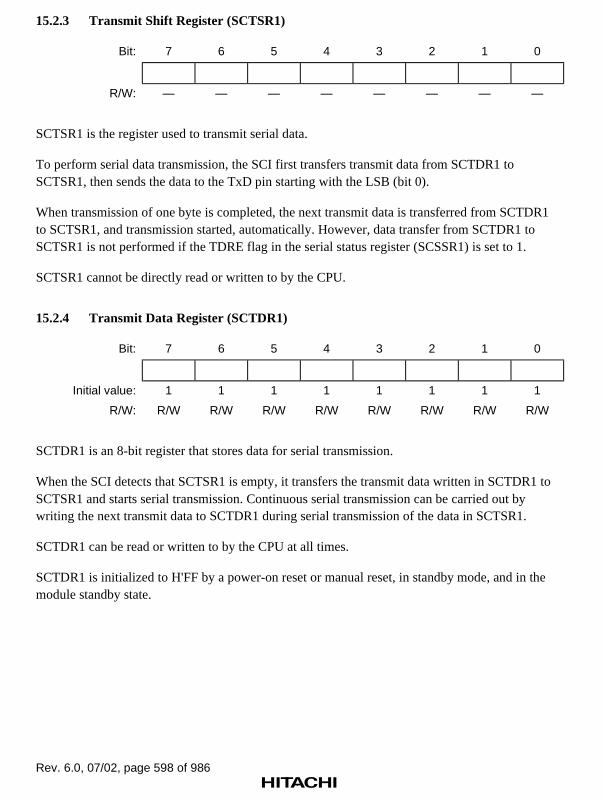
Rev. 6.0, 07/02, page 598 of 986
15.2.3 Transmit Shift Register (SCTSR1)
Bit: 7 6 5 4 3 2 1 0
R/W: — — — — — — — —
SCTSR1 is the register used to transmit serial data.
To perform serial data transmission, the SCI first transfers transmit data from SCTDR1 toSCTSR1, then sends the data to the TxD pin starting with the LSB (bit 0).
When transmission of one byte is completed, the next transmit data is transferred from SCTDR1to SCTSR1, and transmission started, automatically. However, data transfer from SCTDR1 toSCTSR1 is not performed if the TDRE flag in the serial status register (SCSSR1) is set to 1.
SCTSR1 cannot be directly read or written to by the CPU.
15.2.4 Transmit Data Register (SCTDR1)
Bit: 7 6 5 4 3 2 1 0
Initial value: 1 1 1 1 1 1 1 1
R/W: R/W R/W R/W R/W R/W R/W R/W R/W
SCTDR1 is an 8-bit register that stores data for serial transmission.
When the SCI detects that SCTSR1 is empty, it transfers the transmit data written in SCTDR1 toSCTSR1 and starts serial transmission. Continuous serial transmission can be carried out bywriting the next transmit data to SCTDR1 during serial transmission of the data in SCTSR1.
SCTDR1 can be read or written to by the CPU at all times.
SCTDR1 is initialized to H'FF by a power-on reset or manual reset, in standby mode, and in themodule standby state.

Rev. 6.0, 07/02, page 599 of 986
15.2.5 Serial Mode Register (SCSMR1)
Bit: 7 6 5 4 3 2 1 0
C/A CHR PE O/E STOP MP CKS1 CKS0
Initial value: 0 0 0 0 0 0 0 0
R/W: R/W R/W R/W R/W R/W R/W R/W R/W
SCSMR1 is an 8-bit register used to set the SCI’s serial transfer format and select the baud rategenerator clock source.
SCSMR1 can be read or written to by the CPU at all times.
SCSMR1 is initialized to H'00 by a power-on reset or manual reset, in standby mode, and in themodule standby state.
Bit 7—Communication Mode (C/AAAA): Selects asynchronous mode or synchronous mode as theSCI operating mode.
Bit 7: C/AAAA Description
0 Asynchronous mode (Initial value)
1 Synchronous mode
Bit 6—Character Length (CHR): Selects 7 or 8 bits as the data length in asynchronous mode. Insynchronous mode, a fixed data length of 8 bits is used regardless of the CHR setting,
Bit 6: CHR Description
0 8-bit data (Initial value)
1 7-bit data*
Note: * When 7-bit data is selected, the MSB (bit 7) of SCTDR1 is not transmitted.
Bit 5—Parity Enable (PE): In asynchronous mode, selects whether or not parity bit addition isperformed in transmission, and parity bit checking in reception. In synchronous mode, parity bitaddition and checking is not performed, regardless of the PE bit setting.
Bit 5: PE Description
0 Parity bit addition and checking disabled (Initial value)
1 Parity bit addition and checking enabled*
Note: * When the PE bit is set to 1, the parity (even or odd) specified by the O/E bit is added totransmit data before transmission. In reception, the parity bit is checked for the parity (evenor odd) specified by the O/E bit.

Rev. 6.0, 07/02, page 600 of 986
Bit 4—Parity Mode (O/EEEE): Selects either even or odd parity for use in parity addition andchecking. The O/E bit setting is only valid when the PE bit is set to 1, enabling parity bit additionand checking, in asynchronous mode. The O/E bit setting is invalid in synchronous mode, andwhen parity addition and checking is disabled in asynchronous mode.
Bit 4: O/EEEE Description
0 Even parity*1 (Initial value)
1 Odd parity*2
Notes: *1 When even parity is set, parity bit addition is performed in transmission so that the totalnumber of 1-bits in the transmit character plus the parity bit is even. In reception, acheck is performed to see if the total number of 1-bits in the receive character plus theparity bit is even.
*2 When odd parity is set, parity bit addition is performed in transmission so that the totalnumber of 1-bits in the transmit character plus the parity bit is odd. In reception, a checkis performed to see if the total number of 1-bits in the receive character plus the paritybit is odd.
Bit 3—Stop Bit Length (STOP): Selects 1 or 2 bits as the stop bit length in asynchronous mode.The STOP bit setting is only valid in asynchronous mode. If synchronous mode is set, the STOPbit setting is invalid since stop bits are not added.
Bit 3: STOP Description
0 1 stop bit*1 (Initial value)
1 2 stop bits*2
Notes: *1 In transmission, a single 1-bit (stop bit) is added to the end of a transmit characterbefore it is sent.
*2 In transmission, two 1-bits (stop bits) are added to the end of a transmit characterbefore it is sent.
In reception, only the first stop bit is checked, regardless of the STOP bit setting. If the secondstop bit is 1, it is treated as a stop bit; if it is 0, it is treated as the start bit of the next transmitcharacter.

Rev. 6.0, 07/02, page 601 of 986
Bit 2—Multiprocessor Mode (MP): Selects a multiprocessor format. When a multiprocessorformat is selected, the PE bit and O/E bit parity settings are invalid. The MP bit setting is onlyvalid in asynchronous mode; it is invalid in synchronous mode.
For details of the multiprocessor communication function including notes on use, see section15.3.3, Multiprocessor Communication Function.
Bit 2: MP Description
0 Multiprocessor function disabled (Initial value)
1 Multiprocessor format selected
Bits 1 and 0—Clock Select 1 and 0 (CKS1, CKS0): These bits select the clock source for the on-chip baud rate generator. The clock source can be selected from Pφ, Pφ/4, Pφ/16, and Pφ/64,according to the setting of bits CKS1 and CKS0.
For the relation between the clock source, the bit rate register setting, and the baud rate, seesection 15.2.9, Bit Rate Register (SCBRR1).
Bit 1: CKS1 Bit 0: CKS0 Description
0 0 Pφ clock (Initial value)
1 Pφ/4 clock
1 0 Pφ/16 clock
1 Pφ/64 clock
Note: Pφ: Peripheral clock
15.2.6 Serial Control Register (SCSCR1)
Bit: 7 6 5 4 3 2 1 0
TIE RIE TE RE MPIE TEIE CKE1 CKE0
Initial value: 0 0 0 0 0 0 0 0
R/W: R/W R/W R/W R/W R/W R/W R/W R/W
The SCSCR1 register performs enabling or disabling of SCI transfer operations, serial clockoutput in asynchronous mode, and interrupt requests, and selection of the serial clock source.
SCSCR1 can be read or written to by the CPU at all times.
SCSCR1 is initialized to H'00 by a power-on reset or manual reset, in standby mode, and in themodule standby state.

Rev. 6.0, 07/02, page 602 of 986
Bit 7—Transmit Interrupt Enable (TIE): Enables or disables transmit-data-empty interrupt(TXI) request generation when serial transmit data is transferred from SCTDR1 to SCTSR1 andthe TDRE flag in SCSSR1 is set to 1.
Bit 7: TIE Description
0 Transmit-data-empty interrupt (TXI) request disabled* (Initial value)
1 Transmit-data-empty interrupt (TXI) request enabled
Note: * TXI interrupt requests can be cleared by reading 1 from the TDRE flag, then clearing it to 0,or by clearing the TIE bit to 0.
Bit 6—Receive Interrupt Enable (RIE): Enables or disables receive-data-full interrupt (RXI)request and receive-error interrupt (ERI) request generation when serial receive data is transferredfrom SCRSR1 to SCRDR1 and the RDRF flag in SCSSR1 is set to 1.
Bit 6: RIE Description
0 Receive-data-full interrupt (RXI) request and receive-error interrupt (ERI)request disabled* (Initial value)
1 Receive-data-full interrupt (RXI) request and receive-error interrupt (ERI)request enabled
Note: * RXI and ERI interrupt requests can be cleared by reading 1 from the RDRF flag, or theFER, PER, or ORER flag, then clearing the flag to 0, or by clearing the RIE bit to 0.
Bit 5—Transmit Enable (TE): Enables or disables the start of serial transmission by the SCI.
Bit 5: TE Description
0 Transmission disabled*1 (Initial value)
1 Transmission enabled*2
Notes: *1 The TDRE flag in SCSSR1 is fixed at 1.*2 In this state, serial transmission is started when transmit data is written to SCTDR1 and
the TDRE flag in SCSSR1 is cleared to 0.SCSMR1 setting must be performed to decide the transmit format before setting the TEbit to 1.

Rev. 6.0, 07/02, page 603 of 986
Bit 4—Receive Enable (RE): Enables or disables the start of serial reception by the SCI.
Bit 4: RE Description
0 Reception disabled*1 (Initial value)
1 Reception enabled*2
Notes: *1 Clearing the RE bit to 0 does not affect the RDRF, FER, PER, and ORER flags, whichretain their states.
*2 Serial reception is started in this state when a start bit is detected in asynchronousmode or serial clock input is detected in synchronous mode.SCSMR1 setting must be performed to decide the receive format before setting the REbit to 1.
Bit 3—Multiprocessor Interrupt Enable (MPIE): Enables or disables multiprocessor interrupts.The MPIE bit setting is only valid in asynchronous mode when the MP bit in SCSMR1 is set to 1.
The MPIE bit setting is invalid in synchronous mode or when the MP bit is cleared to 0.
Bit 3: MPIE Description
0 Multiprocessor interrupts disabled (normal reception performed) (Initial value)
[Clearing conditions]
• When the MPIE bit is cleared to 0
• When data with MPB = 1 is received
1 Multiprocessor interrupts enabled*
Note: * When receive data including MPB = 1 is received, the MPIE bit is cleared to 0 automatically,and generation of RXI and ERI interrupts (when the TIE and RIE bits in SCSCR1 are set to1) and FER and ORER flag setting is enabled.
Bit 2—Transmit-End interrupt Enable (TEIE): Enables or disables transmit-end interrupt(TEI) request generation when there is no valid transmit data in SCTDR1 at the time for MSB datatransmission.
Bit 2: TEIE Description
0 Transmit-end interrupt (TEI) request disabled* (Initial value)
1 Transmit-end interrupt (TEI) request enabled*
Note: * TEI interrupt requests can be cleared by reading 1 from the TDRE flag in SCSSR1, thenclearing it to 0 and clearing the TEND flag to 0, or by clearing the TEIE bit to 0.
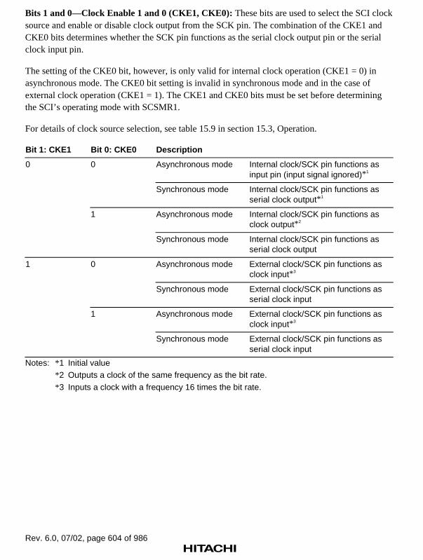
Rev. 6.0, 07/02, page 604 of 986
Bits 1 and 0—Clock Enable 1 and 0 (CKE1, CKE0): These bits are used to select the SCI clocksource and enable or disable clock output from the SCK pin. The combination of the CKE1 andCKE0 bits determines whether the SCK pin functions as the serial clock output pin or the serialclock input pin.
The setting of the CKE0 bit, however, is only valid for internal clock operation (CKE1 = 0) inasynchronous mode. The CKE0 bit setting is invalid in synchronous mode and in the case ofexternal clock operation (CKE1 = 1). The CKE1 and CKE0 bits must be set before determiningthe SCI’s operating mode with SCSMR1.
For details of clock source selection, see table 15.9 in section 15.3, Operation.
Bit 1: CKE1 Bit 0: CKE0 Description
0 0 Asynchronous mode Internal clock/SCK pin functions asinput pin (input signal ignored)*1
Synchronous mode Internal clock/SCK pin functions asserial clock output*1
1 Asynchronous mode Internal clock/SCK pin functions asclock output*2
Synchronous mode Internal clock/SCK pin functions asserial clock output
1 0 Asynchronous mode External clock/SCK pin functions asclock input*3
Synchronous mode External clock/SCK pin functions asserial clock input
1 Asynchronous mode External clock/SCK pin functions asclock input*3
Synchronous mode External clock/SCK pin functions asserial clock input
Notes: *1 Initial value*2 Outputs a clock of the same frequency as the bit rate.
*3 Inputs a clock with a frequency 16 times the bit rate.

Rev. 6.0, 07/02, page 605 of 986
15.2.7 Serial Status Register (SCSSR1)
Bit: 7 6 5 4 3 2 1 0
TDRE RDRF ORER FER PER TEND MPB MPBT
Initial value: 1 0 0 0 0 1 — 0
R/W: R/(W)* R/(W)* R/(W)* R/(W)* R/(W)* R R R/W
Note: * Only 0 can be written, to clear the flag.
SCSSR1 is an 8-bit register containing status flags that indicate the operating status of the SCI,and multiprocessor bits.
SCSSR1 can be read or written to by the CPU at all times. However, 1 cannot be written to flagsTDRE, RDRF, ORER, PER, and FER. Also note that in order to clear these flags they must beread as 1 beforehand. The TEND flag and MPB flag are read-only flags and cannot be modified.
SCSSR1 is initialized to H'84 by a power-on reset or manual reset, in standby mode, and in themodule standby state.
Bit 7—Transmit Data Register Empty (TDRE): Indicates that data has been transferred fromSCTDR1 to SCTSR1 and the next serial transmit data can be written to SCTDR1.
Bit 7: TDRE Description
0 Valid transmit data has been written to SCTDR1
[Clearing conditions]
• When 0 is written to TDRE after reading TDRE = 1
• When data is written to SCTDR1 by the DMAC
1 There is no valid transmit data in SCTDR1 (Initial value)
[Setting conditions]
• Power-on reset, manual reset, standby mode, or module standby
• When the TE bit in SCSCR1 is 0
• When data is transferred from SCTDR1 to SCTSR1 and data can bewritten to SCTDR1

Rev. 6.0, 07/02, page 606 of 986
Bit 6—Receive Data Register Full (RDRF): Indicates that the received data has been stored inSCRDR1.
Bit 6: RDRF Description
0 There is no valid receive data in SCRDR1 (Initial value)
[Clearing conditions]
• Power-on reset, manual reset, standby mode, or module standby
• When 0 is written to RDRF after reading RDRF = 1
• When data in SCRDR1 is read by the DMAC
1 There is valid receive data in SCRDR1
[Setting condition]
When serial reception ends normally and receive data is transferred fromSCRSR1 to SCRDR1
Note: SCRDR1 and the RDRF flag are not affected and retain their previous values when an erroris detected during reception or when the RE bit in SCSCR1 is cleared to 0.If reception of the next data is completed while the RDRF flag is still set to 1, an overrunerror will occur and the receive data will be lost.
Bit 5—Overrun Error (ORER): Indicates that an overrun error occurred during reception,causing abnormal termination.
Bit 5: ORER Description
0 Reception in progress, or reception has ended normally*1 (Initial value)
[Clearing conditions]
• Power-on reset, manual reset, standby mode, or module standby
• When 0 is written to ORER after reading ORER = 1
1 An overrun error occurred during reception*2
[Setting condition]
When the next serial reception is completed while RDRF = 1
Notes: *1 The ORER flag is not affected and retains its previous state when the RE bit inSCSCR1 is cleared to 0.
*2 The receive data prior to the overrun error is retained in SCRDR1, and the datareceived subsequently is lost. Serial reception cannot be continued while the ORER flagis set to 1. In synchronous mode, serial transmission cannot be continued either.

Rev. 6.0, 07/02, page 607 of 986
Bit 4—Framing Error (FER): Indicates that a framing error occurred during reception inasynchronous mode, causing abnormal termination.
Bit 4: FER Description
0 Reception in progress, or reception has ended normally*1 (Initial value)
[Clearing conditions]
• Power-on reset, manual reset, standby mode, or module standby
• When 0 is written to FER after reading FER = 1
1 A framing error occurred during reception
[Setting condition]
When the SCI checks whether the stop bit at the end of the receive data is 1when reception ends, and the stop bit is 0*2
Notes: *1 The FER flag is not affected and retains its previous state when the RE bit in SCSCR1is cleared to 0.
*2 In 2-stop-bit mode, only the first stop bit is checked for a value of 1; the second stop bitis not checked. If a framing error occurs, the receive data is transferred to SCRDR1 butthe RDRF flag is not set. Serial reception cannot be continued while the FER flag is setto 1.
Bit 3—Parity Error (PER): Indicates that a parity error occurred during reception with parityaddition in asynchronous mode, causing abnormal termination.
Bit 3: PER Description
0 Reception in progress, or reception has ended normally*1 (Initial value)
[Clearing conditions]
• Power-on reset, manual reset, standby mode, or module standby
• When 0 is written to PER after reading PER = 1
1 A parity error occurred during reception*2
[Setting condition]
When, in reception, the number of 1-bits in the receive data plus the paritybit does not match the parity setting (even or odd) specified by the O/E bit inSCSMR1
Notes: *1 The PER flag is not affected and retains its previous state when the RE bit in SCSCR1is cleared to 0.
*2 If a parity error occurs, the receive data is transferred to SCRDR1 but the RDRF flag isnot set. Serial reception cannot be continued while the PER flag is set to 1.
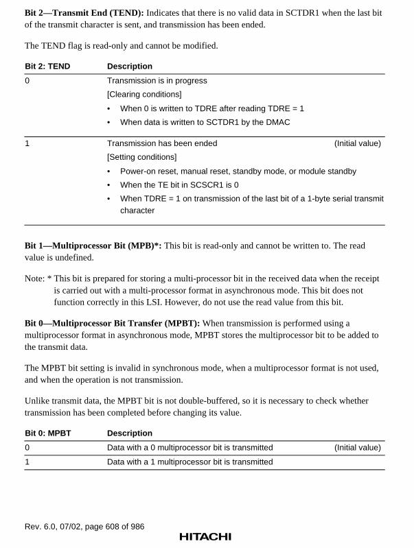
Rev. 6.0, 07/02, page 608 of 986
Bit 2—Transmit End (TEND): Indicates that there is no valid data in SCTDR1 when the last bitof the transmit character is sent, and transmission has been ended.
The TEND flag is read-only and cannot be modified.
Bit 2: TEND Description
0 Transmission is in progress
[Clearing conditions]
• When 0 is written to TDRE after reading TDRE = 1
• When data is written to SCTDR1 by the DMAC
1 Transmission has been ended (Initial value)
[Setting conditions]
• Power-on reset, manual reset, standby mode, or module standby
• When the TE bit in SCSCR1 is 0
• When TDRE = 1 on transmission of the last bit of a 1-byte serial transmitcharacter
Bit 1—Multiprocessor Bit (MPB)*: This bit is read-only and cannot be written to. The readvalue is undefined.
Note: * This bit is prepared for storing a multi-processor bit in the received data when the receiptis carried out with a multi-processor format in asynchronous mode. This bit does notfunction correctly in this LSI. However, do not use the read value from this bit.
Bit 0—Multiprocessor Bit Transfer (MPBT): When transmission is performed using amultiprocessor format in asynchronous mode, MPBT stores the multiprocessor bit to be added tothe transmit data.
The MPBT bit setting is invalid in synchronous mode, when a multiprocessor format is not used,and when the operation is not transmission.
Unlike transmit data, the MPBT bit is not double-buffered, so it is necessary to check whethertransmission has been completed before changing its value.
Bit 0: MPBT Description
0 Data with a 0 multiprocessor bit is transmitted (Initial value)
1 Data with a 1 multiprocessor bit is transmitted
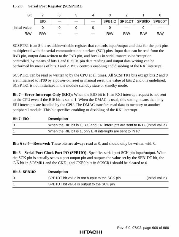
Rev. 6.0, 07/02, page 609 of 986
15.2.8 Serial Port Register (SCSPTR1)
Bit: 7 6 5 4 3 2 1 0
EIO — — — SPB1IO SPB1DT SPB0IO SPB0DT
Initial value: 0 0 0 0 0 — 0 —
R/W: R/W — — — R/W R/W R/W R/W
SCSPTR1 is an 8-bit readable/writable register that controls input/output and data for the port pinsmultiplexed with the serial communication interface (SCI) pins. Input data can be read from theRxD pin, output data written to the TxD pin, and breaks in serial transmission/receptioncontrolled, by means of bits 1 and 0. SCK pin data reading and output data writing can beperformed by means of bits 3 and 2. Bit 7 controls enabling and disabling of the RXI interrupt.
SCSPTR1 can be read or written to by the CPU at all times. All SCSPTR1 bits except bits 2 and 0are initialized to H'00 by a power-on reset or manual reset; the value of bits 2 and 0 is undefined.SCSPTR1 is not initialized in the module standby state or standby mode.
Bit 7—Error Interrupt Only (EIO): When the EIO bit is 1, an RXI interrupt request is not sentto the CPU even if the RIE bit is set to 1. When the DMAC is used, this setting means that onlyERI interrupts are handled by the CPU. The DMAC transfers read data to memory or anotherperipheral module. This bit specifies enabling or disabling of the RXI interrupt.
Bit 7: EIO Description
0 When the RIE bit is 1, RXI and ERI interrupts are sent to INTC(Initial value)
1 When the RIE bit is 1, only ERI interrupts are sent to INTC
Bits 6 to 4—Reserved: These bits are always read as 0, and should only be written with 0.
Bit 3—Serial Port Clock Port I/O (SPB1IO): Specifies serial port SCK pin input/output. Whenthe SCK pin is actually set as a port output pin and outputs the value set by the SPB1DT bit, theC/A bit in SCSMR1 and the CKE1 and CKE0 bits in SCSCR1 should be cleared to 0.
Bit 3: SPB1IO Description
0 SPB1DT bit value is not output to the SCK pin (Initial value)
1 SPB1DT bit value is output to the SCK pin

Rev. 6.0, 07/02, page 610 of 986
Bit 2—Serial Port Clock Port Data (SPB1DT): Specifies the serial port SCK pin input/outputdata. Input or output is specified by the SPB1IO bit (see the description of bit 3, SPB1IO, fordetails). When output is specified, the value of the SPB1DT bit is output to the SCK pin. The SCKpin value is read from the SPB1DT bit regardless of the value of the SPB1IO bit. The initial valueof this bit after a power-on or manual reset is undefined.
Bit 2: SPB1DT Description
0 Input/output data is low-level
1 Input/output data is high-level
Bit 1—Serial Port Break I/O (SPB0IO): Specifies the serial port TxD pin output condition.When the TxD pin is actually set as a port output pin and outputs the value set by the SPB0DT bit,the TE bit in SCSCR1 should be cleared to 0.
Bit 1: SPB0IO Description
0 SPB0DT bit value is not output to the TxD pin (Initial value)
1 SPB0DT bit value is output to the TxD pin
Bit 0—Serial Port Break Data (SPB0DT): Specifies the serial port RxD pin input data and TxDpin output data. The TxD pin output condition is specified by the SPB0IO bit (see the descriptionof bit 1, SPB0IO, for details). When the TxD pin is designated as an output, the value of theSPB0DT bit is output to the TxD pin. The RxD pin value is read from the SPB0DT bit regardlessof the value of the SPB0IO bit. The initial value of this bit after a power-on or manual reset isundefined.
Bit 0: SPB0DT Description
0 Input/output data is low-level
1 Input/output data is high-level
SCI I/O port block diagrams are shown in figures 15.2 to 15.4.

Rev. 6.0, 07/02, page 611 of 986
Reset
Reset
Internal data busSPTRW
SPTRW
SCI
RQ DSPB1IO
C
RQ DSPB1DT
C
SPTRR
Clock output enable signal
Serial clock output signal
Serial clock input signal
Clock input enable signal
*
MD0/SCK
Mode settingregister
SPTRW: Write to SPTRSPTRR: Read SPTR
Note: * Signals that set the SCK pin function as internal clock output or external clock input according to the CKE0 and CKE1 bits in SCSCR1 and the C/ bit in SCSMR1.
Figure 15.2 MD0/SCK Pin

Rev. 6.0, 07/02, page 612 of 986
Reset
Internal data bus
SPTRW
SCI
RQ DSPB0IO
C
Reset
SPTRW
RQ DSPB0DT
C
MD7/TxD
Mode setting register
Transmit enable signal
Serial transmit data
SPTRW: Write to SPTR
Figure 15.3 MD7/TxD Pin
Internal data bus
SCIRxD
SPTRR
Serial receive data
SPTRR: Read SPTR
Figure 15.4 RxD Pin

Rev. 6.0, 07/02, page 613 of 986
15.2.9 Bit Rate Register (SCBRR1)
Bit: 7 6 5 4 3 2 1 0
Initial value: 1 1 1 1 1 1 1 1
R/W: R/W R/W R/W R/W R/W R/W R/W R/W
SCBRR1 is an 8-bit register that sets the serial transfer bit rate in accordance with the baud rategenerator operating clock selected by bits CKS1 and CKS0 in SCSMR1.
SCBRR1 can be read or written to by the CPU at all times.
SCBRR1 is initialized to H'FF by a power-on reset or manual reset, in standby mode, and in themodule standby state.
The SCBRR1 setting is found from the following equations.
Asynchronous mode:
N = × 106 – 164 × 22n–1 × B
φP
Synchronous mode:
N = × 106 – 18 × 22n–1 × B
φP
Where B: Bit rate (bits/s)N: SCBRR1 setting for baud rate generator (0 ≤ N ≤ 255)Pφ: Peripheral module operating frequency (MHz)n: Baud rate generator input clock (n = 0 to 3)
(See the table below for the relation between n and the clock.)
SCSMR1 Setting
n Clock CKS1 CKS0
0 Pφ 0 0
1 Pφ/4 0 1
2 Pφ/16 1 0
3 Pφ/64 1 1

Rev. 6.0, 07/02, page 614 of 986
The bit rate error in asynchronous mode is found from the following equation:
Error (%) = × 100P × 106
(N + 1) × B × 64 × 22n–1φ
– 1
Table 15.3 shows sample SCBRR1 settings in asynchronous mode, and table 15.4 shows sampleSCBRR1 settings in synchronous mode.

Rev. 6.0, 07/02, page 615 of 986
Table 15.3 Examples of Bit Rates and SCBRR1 Settings in Asynchronous Mode
Pφφφφ (MHz)
2 2.097152 2.4576 3
Bit Rate(bits/s) n N
Error(%) n N
Error(%) n N
Error(%) n N
Error(%)
110 1 141 0.03 1 148 –0.04 1 174 –0.26 1 212 0.03
150 1 103 0.16 1 108 0.21 1 127 0.00 1 155 0.16
300 0 207 0.16 0 217 0.21 0 255 0.00 1 77 0.16
600 0 103 0.16 0 108 0.21 0 127 0.00 0 155 0.16
1200 0 51 0.16 0 54 –0.70 0 63 0.00 0 77 0.16
2400 0 25 0.16 0 26 1.14 0 31 0.00 0 38 0.16
4800 0 12 0.16 0 13 –2.48 0 15 0.00 0 19 –2.34
9600 0 6 –6.99 0 6 –2.48 0 7 0.00 0 9 –2.34
19200 0 2 8.51 0 2 13.78 0 3 0.00 0 4 –2.34
31250 0 1 0.00 0 1 4.86 0 1 22.88 0 2 0.00
38400 0 1 –18.62 0 1 –14.67 0 1 0.00
Pφφφφ (MHz)
3.6864 4 4.9152 5
Bit Rate(bits/s) n N
Error(%) n N
Error(%) n N
Error(%) n N
Error(%)
110 2 64 0.70 2 70 0.03 2 86 0.31 2 88 –0.25
150 1 191 0.00 1 207 0.16 1 255 0.00 2 64 0.16
300 1 95 0.00 1 103 0.16 1 127 0.00 1 129 0.16
600 0 191 0.00 0 207 0.16 0 255 0.00 1 64 0.16
1200 0 95 0.00 0 103 0.16 0 127 0.00 0 129 0.16
2400 0 47 0.00 0 51 0.16 0 63 0.00 0 64 0.16
4800 0 23 0.00 0 25 0.16 0 31 0.00 0 32 –1.36
9600 0 11 0.00 0 12 0.16 0 15 0.00 0 15 1.73
19200 0 5 0.00 0 6 –6.99 0 7 0.00 0 7 1.73
31250 — — — 0 3 0.00 0 4 –1.70 0 4 0.00
38400 0 2 0.00 0 2 8.51 0 3 0.00 0 3 1.73
LegendBlank: No setting is available.—: A setting is available but error occurs.

Rev. 6.0, 07/02, page 616 of 986
Table 15.3 Examples of Bit Rates and SCBRR1 Settings in Asynchronous Mode (cont)
Pφφφφ (MHz)
6 6.144 7.37288 8
Bit Rate(bits/s) n N
Error(%) n N
Error(%) n N
Error(%) n N
Error(%)
110 2 106 –0.44 2 108 0.08 2 130 –0.07 2 141 0.03
150 2 77 0.16 2 79 0.00 2 95 0.00 2 103 0.16
300 1 155 0.16 1 159 0.00 1 191 0.00 1 207 0.16
600 1 77 0.16 1 79 0.00 1 95 0.00 1 103 0.16
1200 0 155 0.16 0 159 0.00 0 191 0.00 0 207 0.16
2400 0 77 0.16 0 79 0.00 0 95 0.00 0 103 0.16
4800 0 38 0.16 0 39 0.00 0 47 0.00 0 51 0.16
9600 0 19 –2.34 0 19 0.00 0 23 0.00 0 25 0.16
19200 0 9 –2.34 0 9 0.00 0 11 0.00 0 12 0.16
31250 0 5 0.00 0 5 2.40 0 6 5.33 0 7 0.00
38400 0 4 –2.34 0 4 0.00 0 5 0.00 0 6 –6.99
Pφφφφ (MHz)
9.8304 10 12 12.288
Bit Rate(bits/s) n N
Error(%) n N
Error(%) n N
Error(%) n N
Error(%)
110 2 174 –0.26 2 177 –0.25 2 212 0.03 2 217 0.08
150 2 127 0.00 2 129 0.16 2 155 0.16 2 159 0.00
300 1 255 0.00 2 64 0.16 2 77 0.16 2 79 0.00
600 1 127 0.00 1 129 0.16 1 155 0.16 1 159 0.00
1200 0 255 0.00 1 64 0.16 1 77 0.16 1 79 0.00
2400 0 127 0.00 0 129 0.16 0 155 0.16 0 159 0.00
4800 0 63 0.00 0 64 0.16 0 77 0.16 0 79 0.00
9600 0 31 0.00 0 32 –1.36 0 38 0.16 0 39 0.00
19200 0 15 0.00 0 15 1.73 0 19 0.16 0 19 0.00
31250 0 9 –1.70 0 9 0.00 0 11 0.00 0 11 2.40
38400 0 7 0.00 0 7 1.73 0 9 –2.34 0 9 0.00

Rev. 6.0, 07/02, page 617 of 986
Table 15.3 Examples of Bit Rates and SCBRR1 Settings in Asynchronous Mode (cont)
Pφφφφ (MHz)
14.7456 16 19.6608 20
Bit Rate(bits/s) n N
Error(%) n N
Error(%) n N
Error(%) n N
Error(%)
110 3 64 0.70 3 70 0.03 3 86 0.31 3 88 –0.25
150 2 191 0.00 2 207 0.16 2 255 0.00 3 64 0.16
300 2 95 0.00 2 103 0.16 2 127 0.00 2 129 0.16
600 1 191 0.00 1 207 0.16 1 255 0.00 2 64 0.16
1200 1 95 0.00 1 103 0.16 1 127 0.00 1 129 0.16
2400 0 191 0.00 0 207 0.16 0 255 0.00 1 64 0.16
4800 0 95 0.00 0 103 0.16 0 127 0.00 0 129 0.16
9600 0 47 0.00 0 51 0.16 0 63 0.00 0 64 0.16
19200 0 23 0.00 0 25 0.16 0 31 0.00 0 32 –1.36
31250 0 14 –1.70 0 15 0.00 0 19 –1.70 0 19 0.00
38400 0 11 0.00 0 12 0.16 0 15 0.00 0 15 1.73
Pφφφφ (MHz)
24 24.576 28.7 30
Bit Rate(bits/s) n N
Error(%) n N
Error(%) n N
Error(%) n N
Error(%)
110 3 106 –0.44 3 108 0.08 3 126 0.31 3 132 0.13
150 3 77 0.16 3 79 0.00 3 92 0.46 3 97 –0.35
300 2 155 0.16 2 159 0.00 2 186 –0.08 2 194 0.16
600 2 77 0.16 2 79 0.00 2 92 0.46 2 97 –0.35
1200 1 155 0.16 1 159 0.00 1 186 –0.08 1 194 0.16
2400 1 77 0.16 1 79 0.00 1 92 0.46 1 97 –0.35
4800 0 155 0.16 0 159 0.00 0 186 –0.08 0 194 –1.36
9600 0 77 0.16 0 79 0.00 0 92 0.46 0 97 –0.35
19200 0 38 0.16 0 39 0.00 0 46 –0.61 0 48 –0.35
31250 0 23 0.00 0 24 –1.70 0 28 –1.03 0 29 0.00
38400 0 19 –2.34 0 19 0.00 0 22 1.55 0 23 1.73

Rev. 6.0, 07/02, page 618 of 986
Table 15.4 Examples of Bit Rates and SCBRR1 Settings in Synchronous Mode
Pφφφφ (MHz)
4 8 16 28.7 30
Bit Rate (bits/s) n N n N n N n N n N
10 — — — — — — — — — —
250 2 249 3 124 3 249 — — — —
500 2 124 2 249 3 124 3 223 3 233
1k 1 249 2 124 2 249 3 111 3 116
2.5k 1 99 1 199 2 99 2 178 2 187
5k 0 199 1 99 1 199 2 89 2 93
10k 0 99 0 199 1 99 1 178 1 187
25k 0 39 0 79 0 159 1 71 1 74
50k 0 19 0 39 0 79 0 143 0 149
100k 0 9 0 19 0 39 0 71 0 74
250k 0 3 0 7 0 15 — — 0 29
500k 0 1 0 3 0 7 — — 0 14
1M 0 0* 0 1 0 3 — — — —
2M 0 0* 0 1 — — — —
Note: As far as possible, the setting should be made so that the error is within 1%.LegendBlank: No setting is available.
—: A setting is available but error occurs.* Continuous transmission/reception is not possible.

Rev. 6.0, 07/02, page 619 of 986
Table 15.5 shows the maximum bit rate for various frequencies in asynchronous mode. Tables15.6 and 15.7 show the maximum bit rates with external clock input.
Table 15.5 Maximum Bit Rate for Various Frequencies with Baud Rate Generator(Asynchronous Mode)
Settings
Pφφφφ (MHz) Maximum Bit Rate (bits/s) n N
2 62500 0 0
2.097152 65536 0 0
2.4576 76800 0 0
3 93750 0 0
3.6864 115200 0 0
4 125000 0 0
4.9152 153600 0 0
8 250000 0 0
9.8304 307200 0 0
12 375000 0 0
14.7456 460800 0 0
16 500000 0 0
19.6608 614400 0 0
20 625000 0 0
24 750000 0 0
24.576 768000 0 0
28.7 896875 0 0
30 937500 0 0

Rev. 6.0, 07/02, page 620 of 986
Table 15.6 Maximum Bit Rate with External Clock Input (Asynchronous Mode)
Pφφφφ (MHz) External Input Clock (MHz) Maximum Bit Rate (bits/s)
2 0.5000 31250
2.097152 0.5243 32768
2.4576 0.6144 38400
3 0.7500 46875
3.6864 0.9216 57600
4 1.0000 62500
4.9152 1.2288 76800
8 2.0000 125000
9.8304 2.4576 153600
12 3.0000 187500
14.7456 3.6864 230400
16 4.0000 250000
19.6608 4.9152 307200
20 5.0000 312500
24 6.0000 375000
24.576 6.1440 384000
28.7 7.1750 448436
30 7.5000 468750
Table 15.7 Maximum Bit Rate with External Clock Input (Synchronous Mode)
Pφφφφ (MHz) External Input Clock (MHz) Maximum Bit Rate (bits/s)
8 1.3333 1333333.3
16 2.6667 2666666.7
24 4.0000 4000000.0
28.7 4.7833 4783333.3
30 5.0000 5000000.0

Rev. 6.0, 07/02, page 621 of 986
15.3 Operation
15.3.1 Overview
The SCI can carry out serial communication in two modes: asynchronous mode in whichsynchronization is achieved character by character, and synchronous mode in whichsynchronization is achieved with clock pulses.
Selection of asynchronous or synchronous mode and the transmission format is made usingSCSMR1 as shown in table 15.8. The SCI clock source is determined by a combination of the C/Abit in SCSMR1 and the CKE1 and CKE0 bits in SCSCR1, as shown in table 15.9.
• Asynchronous mode
Data length: Choice of 7 or 8 bits
Choice of parity addition, multiprocessor bit addition, and addition of 1 or 2 stop bits (thecombination of these parameters determines the transfer format and character length)
Detection of framing, parity, and overrun errors, and breaks, during reception
Choice of internal or external clock as SCI clock source
When internal clock is selected: The SCI operates on the baud rate generator clock and aclock with the same frequency as the bit rate can be output.
When external clock is selected: A clock with a frequency of 16 times the bit rate must beinput (the on-chip baud rate generator is not used).
• Synchronous mode
Transfer format: Fixed 8-bit data
Detection of overrun errors during reception
Choice of internal or external clock as SCI clock source
When internal clock is selected: The SCI operates on the baud rate generator clock and aserial clock is output off-chip.
When external clock is selected: The on-chip baud rate generator is not used, and the SCIoperates on the input serial clock.

Rev. 6.0, 07/02, page 622 of 986
Table 15.8 SCSMR1 Settings for Serial Transfer Format Selection
SCSMR1 Settings SCI Transfer Format
Bit 7:C/AAAA
Bit 6:CHR
Bit 2:MP
Bit 5:PE
Bit 3:STOP Mode
DataLength
Multi-processorBit
ParityBit
Stop BitLength
0 0 0 0 0 8-bit data No No 1 bit
1 2 bits
1 0 Yes 1 bit
1 2 bits
1 0 0 7-bit data No 1 bit
1 2 bits
1 0 Yes 1 bit
1
Asynchronousmode
2 bits
0 1 * 0 8-bit data Yes No 1 bit
1 2 bits
1 0 7-bit data 1 bit
1
Asynchronousmode(multiprocessorformat)
2 bits
1 * * * * Synchronousmode
8-bit data No None
Note: An asterisk in the table means “Don’t care.”
Table 15.9 SCSMR1 and SCSCR1 Settings for SCI Clock Source Selection
SCSMR1 SCSCR1 Setting SCI Transmit/Receive Clock
Bit 7:C/AAAA
Bit 1:CKE1
Bit 0:CKE0 Mode
ClockSource SCK Pin Function
0 0 0 Internal SCI does not use SCK pin
1 Outputs clock with samefrequency as bit rate
1 0 External Inputs clock with frequency of16 times the bit rate
1
Asynchronousmode
1 0 0 Internal Outputs serial clock
1
1 0 External Inputs serial clock
1
Synchronousmode

Rev. 6.0, 07/02, page 623 of 986
15.3.2 Operation in Asynchronous Mode
In asynchronous mode, characters are sent or received, each preceded by a start bit indicating thestart of communication and followed by one or two stop bits indicating the end of communication.Serial communication is thus carried out with synchronization established on a character-by-character basis.
Inside the SCI, the transmitter and receiver are independent units, enabling full-duplexcommunication. Both the transmitter and the receiver also have a double-buffered structure, sothat data can be read or written during transmission or reception, enabling continuous datatransfer.
Figure 15.5 shows the general format for asynchronous serial communication.
In asynchronous serial communication, the transmission line is usually held in the mark state (highlevel). The SCI monitors the transmission line, and when it goes to the space state (low level),recognizes a start bit and starts serial communication.
One serial communication character consists of a start bit (low level), followed by data (in LSB-first order), a parity bit (high or low level), and finally one or two stop bits (high level).
In asynchronous mode, the SCI performs synchronization at the falling edge of the start bit inreception. The SCI samples the data on the eighth pulse of a clock with a frequency of 16 timesthe length of one bit, so that the transfer data is latched at the center of each bit.
Serial data
(LSB)
7 or 8 bits
One unit of transfer data (character or frame)
Paritybit
1 bit, or none
1 or 2 bits
Stop bit(s)
1 1
0 D0 D1 D2 D3 D4 D5 D6 D7 0/1 1 1
Idle state (mark state)
Start bit
1 bit
(MSB)
Transmit/receive data
Figure 15.5 Data Format in Asynchronous Communication (Example with 8-Bit Data,Parity, Two Stop Bits)
Data Transfer Format
Table 15.10 shows the data transfer formats that can be used in asynchronous mode. Any of 12transfer formats can be selected according to the SCSMR1 setting.

Rev. 6.0, 07/02, page 624 of 986
Table 15.10 Serial Transfer Formats (Asynchronous Mode)
SCSMR1 Settings Serial Transfer Format and Frame Length
CHR PE MP STOP 1 2 3 4 5 6 7 8 9 10 11 12
0 0 0 0 S 8-bit data STOP
0 0 0 1 S 8-bit data STOP STOP
0 1 0 0 S 8-bit data P STOP
0 1 0 1 S 8-bit data P STOP STOP
1 0 0 0 S 7-bit data STOP
1 0 0 1 S 7-bit data STOP STOP
1 1 0 0 S 7-bit data P STOP
1 1 0 1 S 7-bit data P STOP STOP
0 * 1 0 S 8-bit data MPB STOP
0 * 1 1 S 8-bit data MPB STOP STOP
1 * 1 0 S 7-bit data MPB STOP
1 * 1 1 S 7-bit data MPB STOP STOP
S: Start bit
STOP: Stop bitP: Parity bitMPB: Multiprocessor bit
Note: An asterisk in the table means “Don’t care.”

Rev. 6.0, 07/02, page 625 of 986
Clock
Either an internal clock generated by the on-chip baud rate generator or an external clock input atthe SCK pin can be selected as the SCI’s serial clock, according to the setting of the C/A bit inSCSMR1 and the CKE1 and CKE0 bits in SCSCR1. For details of SCI clock source selection, seetable 15.9.
When an external clock is input at the SCK pin, the clock frequency should be 16 times the bit rateused.
When the SCI is operated on an internal clock, the clock can be output from the SCK pin. Thefrequency of the clock output in this case is equal to the bit rate, and the phase is such that therising edge of the clock is at the center of each transmit data bit, as shown in figure 15.6.
D0 D1 D2 D3 D4 D5 D6 D7 0/1 1 1
One frame
0
Figure 15.6 Relation between Output Clock and Transfer Data Phase(Asynchronous Mode)
Data Transfer Operations
SCI Initialization (Asynchronous Mode): Before transmitting and receiving data, it is necessaryto clear the TE and RE bits in SCSCR1 to 0, then initialize the SCI as described below.
When the operating mode, transfer format, etc., is changed, the TE and RE bits must be cleared to0 before making the change using the following procedure. When the TE bit is cleared to 0, theTDRE flag is set to 1 and SCTSR1 is initialized. Note that clearing the RE bit to 0 does not changethe contents of the RDRF, PER, FER, and ORER flags, or the contents of SCRDR1.
When an external clock is used the clock should not be stopped during operation, includinginitialization, since operation will be unreliable in this case.
Figure 15.7 shows a sample SCI initialization flowchart.

Rev. 6.0, 07/02, page 626 of 986
Initialization
Clear TE and RE bitsin SCSCR1 to 0
Set CKE1 and CKE0 bitsin SCSCR1 (leaving TE and
RE bits cleared to 0)
Set transmit/receive formatin SCSMR1
Set value in SCBRR1
1-bit interval elapsed?
Set TE and RE bits in SCSCR1 to 1, and set RIE, TIE, TEIE,
and MPIE bits
End
Yes
Wait
No
1. Set the clock selection in SCSCR1.
Be sure to clear bits RIE, TIE, TEIE, and MPIE, and bits TE and RE, to 0.
When clock output is selected in asynchronous mode, it is output immediately after SCSCR1 settings are made.
2. Set the transmit/receive format in SCSMR1.
3. Write a value corresponding to the bit rate into SCBRR1. (Not necessary if an external clock is used.)
4. Wait at least one bit interval, then set the TE bit or RE bit in SCSCR1 to 1. Also set the RIE, TIE, TEIE, and MPIE bits.
Setting the TE and RE bits enables the TxD and RxD pins to be used. When transmitting, the SCI will go to the mark state; when receiving, it will go to the idle state, waiting for a start bit.
Figure 15.7 Sample SCI Initialization Flowchart
Serial Data Transmission (Asynchronous Mode): Figure 15.8 shows a sample flowchart forserial transmission.
Use the following procedure for serial data transmission after enabling the SCI for transmission.

Rev. 6.0, 07/02, page 627 of 986
Start of transmission
Read TDRE flag in SCSSR1
TDRE = 1?
All data transmitted?
TEND = 1?
Break output?
Clear TE bit in SCSCR1 to 0
End of transmission
Yes
No
Yes
No
Yes
No
Yes
No
Write transmit data to SCTDR1and clear TDRE flag
in SCSSR1 to 0
Read TEND flag in SCSSR1
Clear SPB0DT to 0 andset SPB0IO to 1
1. SCI status check and transmit data write: Read SCSSR1 and check that the TDRE flag is set to 1, then write transmit data to SCTDR1 and clear the TDRE flag to 0.
2. Serial transmission continuation procedure: To continue serial transmission, read 1 from the TDRE flag to confirm that writing is possible, then write data to SCTDR1, and then clear the TDRE flag to 0. (Checking and clearing of the TDRE flag is automatic when the direct memory access controller (DMAC) is activated by a transmit-data-empty interrupt (TXI) request, and data is written to SCTDR1.)
3. Break output at the end of serial transmission: To output a break in serial transmission, clear the SPB0DT bit to 0 and set the SPB0IO bit to 1 in SCSPTR, then clear the TE bit in SCSCR1 to 0.
Figure 15.8 Sample Serial Transmission Flowchart

Rev. 6.0, 07/02, page 628 of 986
In serial transmission, the SCI operates as described below.
1. The SCI monitors the TDRE flag in SCSSR1. When TDRE is cleared to 0, the SCI recognizesthat data has been written to SCTDR1, and transfers the data from SCTDR1 to SCTSR1.
2. After transferring data from SCTDR1 to SCTSR1, the SCI sets the TDRE flag to 1 and startstransmission. If the TIE bit is set to 1 at this time, a transmit-data-empty interrupt (TXI) isgenerated.
The serial transmit data is sent from the TxD pin in the following order.
a. Start bit: One 0-bit is output.
b. Transmit data: 8-bit or 7-bit data is output in LSB-first order.
c. Parity bit or multiprocessor bit: One parity bit (even or odd parity), or one multiprocessorbit is output. (A format in which neither a parity bit nor a multiprocessor bit is output canalso be selected.)
d. Stop bit(s): One or two 1-bits (stop bits) are output.
e. Mark state: 1 is output continuously until the start bit that starts the next transmission issent.
3. The SCI checks the TDRE flag at the timing for sending the stop bit. If the TDRE flag iscleared to 0, data is transferred from SCTDR1 to SCTSR1, the stop bit is sent, and then serialtransmission of the next frame is started.
If the TDRE flag is set to 1, the TEND flag in SCSSR1 is set to 1, the stop bit is sent, and thenthe line goes to the mark state in which 1 is output continuously. If the TEIE bit in SCSCR1 isset to 1 at this time, a TEI interrupt request is generated.
Figure 15.9 shows an example of the operation for transmission in asynchronous mode.
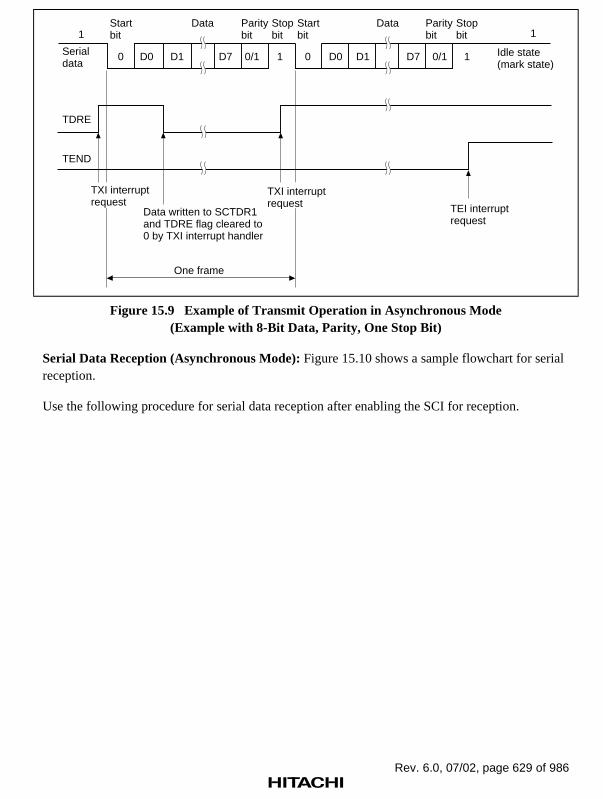
Rev. 6.0, 07/02, page 629 of 986
1
0 D0 D1 D7 0/1 1 0 D0 D1 D7 0/1 1
1
TDRE
TEND
Serial data
Start bit
Data Parity bit
Stop bit
Start bit
Idle state (mark state)
Data Parity bit
Stop bit
TXI interrupt request
Data written to SCTDR1and TDRE flag cleared to0 by TXI interrupt handler
One frame
TEI interrupt request
TXI interrupt request
Figure 15.9 Example of Transmit Operation in Asynchronous Mode(Example with 8-Bit Data, Parity, One Stop Bit)
Serial Data Reception (Asynchronous Mode): Figure 15.10 shows a sample flowchart for serialreception.
Use the following procedure for serial data reception after enabling the SCI for reception.

Rev. 6.0, 07/02, page 630 of 986
Start of reception
Read ORER, PER, and FER flagsin SCSSR1
Read RDRF flag in SCSSR1
PER or FER or ORER = 1?
RDRF = 1?
All data received?
Clear RE bit in SCSCR1 to 0
End of reception
Error handling
Yes
No
Yes
No
Yes
No
Read receive data in SCRDR1,and clear RDRF flag
in SCSSR1 to 0
1. Receive error handling and break detection: If a receive error occurs, read the ORER, PER, and FER flags in SCSSR1 to identify the error. After performing the appropriate error handling, ensure that the ORER, PER, and FER flags are all cleared to 0. Reception cannot be resumed if any of these flags are set to 1. In the case of a framing error, a break can be detected by reading the value of the RxD pin.
2. SCI status check and receive data read : Read SCSSR1 and check that RDRF = 1, then read the receive data in SCRDR1 and clear the RDRF flag to 0.
3. Serial reception continuation procedure: To continue serial reception, complete zero-clearing of the RDRF flag before the stop bit for the current frame is received. (The RDRF flag is cleared automatically when the direct memory access controller (DMAC) is activated by an RXI interrupt and the SCRDR1 value is read.)
Figure 15.10 Sample Serial Reception Flowchart (1)

Rev. 6.0, 07/02, page 631 of 986
Error handling
ORER = 1?
FER = 1?
Break?
PER = 1?
End
Yes
Yes
No
Yes
No
No
No
Yes
Clear ORER, PER, and FER flagsin SCSSR1 to 0
Parity error handling
Framing error handling Clear RE bit in SCSCR1 to 0
Overrun error handling
Figure 15.10 Sample Serial Reception Flowchart (2)

Rev. 6.0, 07/02, page 632 of 986
In serial reception, the SCI operates as described below.
1. The SCI monitors the transmission line, and if a 0 start bit is detected, performs internalsynchronization and starts reception.
2. The received data is stored in SCRSR1 in LSB-to-MSB order.
3. The parity bit and stop bit are received.
After receiving these bits, the SCI carries out the following checks.
a. Parity check: The SCI checks whether the number of 1-bits in the receive data agrees withthe parity (even or odd) set in the O/E bit in SCSMR1.
b. Stop bit check: The SCI checks whether the stop bit is 1. If there are two stop bits, only thefirst is checked.
c. Status check: The SCI checks whether the RDRF flag is 0, indicating that the receive datacan be transferred from SCRSR1 to SCRDR1.
If all the above checks are passed, the RDRF flag is set to 1, and the receive data is stored inSCRDR1.
If a receive error is detected in the error check, the operation is as shown in table 15.11.
Note: No further receive operations can be performed when a receive error has occurred. Alsonote that the RDRF flag is not set to 1 in reception, and so the error flags must be clearedto 0.
4. If the EIO bit in SCSPTR1 is cleared to 0 and the RIE bit in SCSCR1 is set to 1 when theRDRF flag changes to 1, a receive-data-full interrupt (RXI) request is generated.
If the RIE bit in SCSCR1 is set to 1 when the ORER, PER, or FER flag changes to 1, areceive-error interrupt (ERI) request is generated. A receive-data-full request is always outputto the DMAC when the RDRF flag changes to 1.
Table 15.11 Receive Error Conditions
Receive Error Abbreviation Condition Data Transfer
Overrun error ORER Reception of next data iscompleted while RDRF flagin SCSSR1 is set to 1
Receive data is not transferredfrom SCRSR1 to SCRDR1
Framing error FER Stop bit is 0 Receive data is transferredfrom SCRSR1 to SCRDR1
Parity error PER Received data parity differsfrom that (even or odd) setin SCSMR1
Receive data is transferredfrom SCRSR1 to SCRDR1
Figure 15.11 shows an example of the operation for reception in asynchronous mode.

Rev. 6.0, 07/02, page 633 of 986
1
0 D0 D1 D7 0/1 1 0 D0 D1 D7 0/1 0/10
RDRF
FER
Serial data
Start bit
Data Parity bit
Stop bit
Start bit
Data Parity bit
Stop bit
RXI interrupt request
One frame
SCRDR1 data read and RDRF flag cleared to 0 by RXI interrupt handler
ERI interrupt request generated by framing error
Figure 15.11 Example of SCI Receive Operation(Example with 8-Bit Data, Parity, One Stop Bit)

Rev. 6.0, 07/02, page 634 of 986
15.3.3 Multiprocessor Communication Function
The multiprocessor communication function performs serial communication using amultiprocessor format, in which a multiprocessor bit is added to the transfer data, in asynchronousmode. Use of this function enables data transfer to be performed among a number of processorssharing a serial transmission line.
When multiprocessor communication is carried out, each receiving station is addressed by aunique ID code.
The serial communication cycle consists of two cycles: an ID transmission cycle which specifiesthe receiving station , and a data transmission cycle. The multiprocessor bit is used to differentiatebetween the ID transmission cycle and the data transmission cycle.
The transmitting station first sends the ID of the receiving station with which it wants to performserial communication as data with a 1 multiprocessor bit added. It then sends transmit data as datawith a 0 multiprocessor bit added.
The receiving station skips the data until data with a 1 multiprocessor bit is sent*.
When data with a 1 multiprocessor bit is received, the receiving station compares that data with itsown ID. The station whose ID matches then receives the data sent next. Stations whose ID doesnot match continue to skip the data until data with a 1 multiprocessor bit is again received*. In thisway, data communication is carried out among a number of processors.
Figure 15.12 shows an example of inter-processor communication using a multiprocessor format.
Note: * With this LSI, the RDRF flag in SCSSR1 is also set to 1 when data with a 0multiprocessor bit transmitted to another station is received. When the RDRF flag inSCSSR1 is set to 1, check the state of the MPIE bit in SCSCR1 with the exceptionhandling routine, and if the MPIE bit is 1, skip the data. That is to say, data skipping isimplemented in cooperation with the exception handling routine.

Rev. 6.0, 07/02, page 635 of 986
Transmittingstation
Receivingstation A
Receivingstation B
Receivingstation C
Receivingstation D
(ID = 01) (ID = 02) (ID = 03) (ID = 04)
Serial transmission line
(MPB = 1) (MPB = 0)
H'01 H'AA
MPB: Multiprocessor bit
Serial data
ID transmission cycle: Receiving station specification
Data transmission cycle: Data transmission to receiving station specified by ID
Figure 15.12 Example of Inter-Processor Communication Using Multiprocessor Format(Transmission of Data H'AA to Receiving Station A)
Data Transfer Formats
There are four data transfer formats. When the multiprocessor format is specified, the parity bitspecification is invalid. For details, see table 15.10.
Clock
See the description under Clock in section 15.3.2.
Data Transfer Operations
Multiprocessor Serial Data Transmission: Figure 15.13 shows a sample flowchart formultiprocessor serial data transmission.
Use the following procedure for multiprocessor serial data transmission after enabling the SCI fortransmission.

Rev. 6.0, 07/02, page 636 of 986
Start of transmission
Read TEND flag in SCSSR1
TEND = 1?
Clear TDRE flag to 0
Read TEND flag in SCSSR1
TEND = 1?
Clear MPBT bit in SCSSR1 to 0
Write data to SCTDR1
Clear TDRE flag to 0
Read TDRE flag in SCSSR1
End of transmission
No
Yes
No
Yes
All data transmitted?
TDRE = 1?
Yes
Yes
No
No
Set MPBT bit in SCSSR1 to 1 andwrite ID data to SCTDR1
1. SCI status check and ID data write: Read SCSSR1 and check that the TEND flag is set to 1, then set the MPBT bit in SCSSR1 to 1 and write ID data to SCTDR1. Finally, clear the TDRE flag to 0.
2. Preparation for data transfer: Read SCSSR1 and check that the TEND flag is set to 1, then set the MPBT bit in SCSSR1 to 1.
3. Serial data transmission: Write the first transmit data to SCTDR1, then clear the TDRE flag to 0.
To continue data transmission, be sure to read 1 from the TDRE flag to confirm that writing is possible, then write data to SCTDR1, and then clear the TDRE flag to 0. (Checking and clearing of the TDRE flag is automatic when the direct memory access controller (DMAC) is activated by a transmit-data-empty interrupt (TXI) request, and data is written to SCTDR1.)
Figure 15.13 Sample Multiprocessor Serial Transmission Flowchart

Rev. 6.0, 07/02, page 637 of 986
In serial transmission, the SCI operates as described below.
1. The SCI monitors the TDRE flag in SCSSR1. When TDRE is cleared to 0, the SCI recognizesthat data has been written to SCTDR1, and transfers the data from SCTDR1 to SCTSR1.
2. After transferring data from SCTDR1 to SCTSR1, the SCI sets the TDRE flag to 1 and startstransmission.
The serial transmit data is sent from the TxD pin in the following order.
a. Start bit: One 0-bit is output.
b. Transmit data: 8-bit or 7-bit data is output in LSB-first order.
c. Multiprocessor bit: One multiprocessor bit (MPBT value) is output.
d. Stop bit(s): One or two 1-bits (stop bits) are output.
e. Mark state: 1 is output continuously until the start bit that starts the next transmission issent.
3. The SCI checks the TDRE flag at the timing for sending the stop bit. If the TDRE flag is set to1, the TEND flag in SCSSR1 is set to 1, the stop bit is sent, and then the line goes to the markstate in which 1 is output. If the TEIE bit in SCSCR1 is set to 1 at this time, a transmit-endinterrupt (TEI) request is generated.
4. The SCI monitors the TDRE flag. When TDRE is cleared to 0, the SCI recognizes that datahas been written to SCTDR1, and transfers the data from SCTDR1 to SCTSR1.
5. After transferring data from SCTDR1 to SCTSR1, the SCI sets the TDRE flag to 1 and startstransmitting. If the transmit-data-empty interrupt enable bit (TIE bit) in SCSCR1 is set to 1 atthis time, a transmit-data-empty interrupt (TXI) request is generated.
The order of transmission is the same as in step 2.
Figure 15.14 shows an example of SCI operation for transmission using a multiprocessor format.

Rev. 6.0, 07/02, page 638 of 986
Serial data
MPBT bit cleared to 0, data written to SCTDR1, and TDRE flag cleared to 0 by TEI interrupt handler
Data written to SCTDR1 and TDRE flag cleared to 0 by TXI interrupt handler
TXI interrupt request TEI interrupt
request
1 1
0 D0 D1 D7 0 00D0 D1 D7 0D0 D1 D71 1 1
Multi-proces-sor bit
Multi-proces-sor bit
Multi-proces-sor bit
Stop bit
Start bit
Stop bit
Stop bit
Start bit
Data Data DataStart bit
TDRE
TEND
One frame
Idle state(mark state)
Figure 15.14 Example of SCI Transmit Operation (Example with 8-Bit Data,Multiprocessor Bit, One Stop Bit)
Multiprocessor Serial Data Reception: Figure 15.15 shows a sample flowchart formultiprocessor serial reception.
Use the following procedure for multiprocessor serial data reception after enabling the SCI forreception.

Rev. 6.0, 07/02, page 639 of 986
Start of reception
Set MPIE bit in SCSCR1 to 1
Read ORER and FER flagsin SCSSR1
FER = 1 or ORER = 1?
Read RDRF flag in SCSSR1Read MPIE bit in SCSCR1
RDRF = 1 and MPIE = 0?
Read receive data in SCRDR1
This station’s ID?
FER = 1 or ORER = 1?
Read RDRF flag in SCSSR1
RDRF = 1?
Read receive data in SCRDR1
All data received?
End of reception
Error handling
Yes
No
Yes
No
Yes
No
Yes
No
No
No
Yes
Yes
Read ORER and FER flagsin SCSSR1
1. ID reception cycle: Set the MPIE bit in SCSCR1 to 1.
2. SCI status check, ID reception and comparison: Read SCSSR1 and SCSCR1, and check that the RDRF flag is set to 1 and MPIE bit is set to 0, then read the receive data in SCRDR1 and compare it with this station’s ID.
If the data is not this station’s ID, set the MPIE bit to 1 again, and clear the RDRF flag to 0. If the data is this station’s ID, clear the RDRF flag to 0.
3. SCI status check and data reception: Read SCSSR1 and check that the RDRF flag is set to 1, then read the data in SCRDR1.
4. Receive error handling and break detection: If a receive error occurs, read the ORER and FER flags in SCSSR1 to identify the error. After performing the appropriate error handling, ensure that the ORER and FER flags are all cleared to 0. Reception cannot be resumed if either of these flags is set to 1. In the case of a framing error, a break can be detected by reading the RxD pin value.
Figure 15.15 Sample Multiprocessor Serial Reception Flowchart (1)

Rev. 6.0, 07/02, page 640 of 986
ORER = 1?
FER = 1?
Error handling
Overrun error handling
Break?
Framing error handling Clear RE bit in SCSCR1 to 0
Clear ORER and FER flags in SCSSR1 to 0
End
Yes
No
No
Yes
Yes
No
Figure 15.15 Sample Multiprocessor Serial Reception Flowchart (2)

Rev. 6.0, 07/02, page 641 of 986
Figure 15.16 shows an example of SCI operation for multiprocessor format reception.
1
0 D0 D1 D7 1 1 0 D0 D1 D7 0 1
1MPB
MPIE
RDRF
ID1 ID2 Data2
1
0 D0 D1 D7 1 1 0 D0 D1 D7 0 1
1MPB MPB
MPIE
RDRF
SCRDR1 value ID1
Serial data
Start bit Data (ID1)
Stop bit
Start bit
Idle state (mark state)
Data(Data1)
Stop bit
(b) Data matches station’s ID
RXI interrupt request(multiprocessor interrupt)MPIE = 0
SCRDR1 data read and RDRF flag cleared to 0 by RXI interrupt handler
As data is not this station’s ID, MPIE bit is set to 1 again
RXI interrupt request
The RDRF flag is cleared to 0 by the RXI interrupt handler.
MPB
Serial data
Start bit Data (ID2)
Stop bit
Start bit
Data(Data2)
Stop bit
Idle state (mark state)
(a) Data does not match station’s ID
SCRDR1 value
RXI interrupt request (multiprocessor interrupt)MPIE = 0
SCRDR1 data read and RDRF flag cleared to 0 by RXI interrupt handler
As data matches this station’s ID, reception continues and data is received by RXI interrupt handler
MPIE bit set to 1 again
Figure 15.16 Example of SCI Receive Operation (Example with 8-Bit Data, MultiprocessorBit, One Stop Bit)

Rev. 6.0, 07/02, page 642 of 986
In multiprocessor mode serial reception, the SCI operates as described below.
1. The SCI monitors the transmission line, and if a 0 start bit is detected, performs internalsynchronization and starts reception.
2. The received data is stored in SCRSR1 in LSB-to-MSB order.
3. If the MPIE bit is 1, MPIE is cleared to 0 when a 1 is received in the multiprocessor bitposition. If the multiprocessor bit is 0, the MPIE bit is not changed.
4. If the MPIE bit is 0, RDRF is checked at the stop bit position, and if RDRF is 1 the overrunerror bit is set. If the stop bit is not 0, the framing error bit is set. If RDRF is 0, the value inSCRSR1 is transferred to SCRDR1, and if the stop bit is 0, RDRF is set to 1.
15.3.4 Operation in Synchronous Mode
In synchronous mode, data is transmitted or received in synchronization with clock pulses, makingit suitable for high-speed serial communication.
Inside the SCI, the transmitter and receiver are independent units, enabling full-duplexcommunication. Both the transmitter and the receiver also have a double-buffered structure, sothat data can be read or written during transmission or reception, enabling continuous datatransfer.
Figure 15.17 shows the general format for synchronous serial communication.
One unit of transfer data (character or frame)
Note: * High except in continuous transmission/reception
Serial clock
Serial data
LSB
Bit 0
MSB
* *
Bit 1 Bit 2 Bit 3 Bit 4 Bit 5 Bit 6 Bit 7 Don’t careDon’t care
Figure 15.17 Data Format in Synchronous Communication
In synchronous serial communication, data on the transmission line is output from one falling edgeof the serial clock to the next. Data confirmation is guaranteed at the rising edge of the serialclock.

Rev. 6.0, 07/02, page 643 of 986
In serial communication, one character consists of data output starting with the LSB and endingwith the MSB. After the MSB is output, the transmission line holds the MSB state.
In synchronous mode, the SCI receives data in synchronization with the falling edge of the serialclock.
Data Transfer Format
A fixed 8-bit data format is used. No parity or multiprocessor bits are added.
Clock
Either an internal clock generated by the on-chip baud rate generator or an external serial clockinput at the SCK pin can be selected, according to the setting of the C/A bit in SCSMR1 and theCKE1 and CKE0 bits in SCSCR1. For details of SCI clock source selection, see table 15.9.
When the SCI is operated on an internal clock, the serial clock is output from the SCK pin.
Eight serial clock pulses are output in the transfer of one character, and when no transfer isperformed the clock is fixed high. In reception only, if an on-chip clock source is selected, clockpulses are output while RE = 1. When the last data is received, RE should be cleared to 0 beforethe end of bit 7.
Data Transfer Operations
SCI Initialization (Synchronous Mode): Before transmitting and receiving data, it is necessaryto clear the TE and RE bits in SCSCR1 to 0, then initialize the SCI as described below.
When the operating mode, transfer format, etc., is changed, the TE and RE bits must be cleared to0 before making the change using the following procedure. When the TE bit is cleared to 0, theTDRE flag is set to 1 and SCTSR1 is initialized. Note that clearing the RE bit to 0 does not changethe contents of the RDRF, PER, FER, and ORER flags, or the contents of SCRDR1.
Figure 15.18 shows a sample SCI initialization flowchart.

Rev. 6.0, 07/02, page 644 of 986
Set transmit/receive formatin SCSMR1
1-bit interval elapsed?
End
No
Wait
Yes
Set TE and RE bits in SCSCR1to 1, and set RIE, TIE, TEIE,
and MPIE bits
Set value in SCBRR1
Set RIE, TIE, TEIE, MPIE, CKE1,and CKE0 bits in SCSCR1
(leaving TE and RE bitscleared to 0)
Clear TE and RE bitsin SCSCR1 to 0
Initialization 1. Set the clock selection in SCSCR1. Be sure to clear bits RIE, TIE, TEIE, and MPIE, TE and RE, to 0.
2. Set transmit/receive format in SCSMR1.
3. Write a value corresponding to the bit rate into SCBRR1. (Not necessary if an external clock is used.)
4. Wait at least one bit interval, then set the TE bit or RE bit in SCSCR1 to 1.
Also set the RIE, TIE, TEIE, and MPIE bits. Setting the TE and RE bits enables the TxD and RxD pins to be used.
Figure 15.18 Sample SCI Initialization Flowchart

Rev. 6.0, 07/02, page 645 of 986
Serial Data Transmission (Synchronous Mode): Figure 15.19 shows a sample flowchart forserial transmission.
Use the following procedure for serial data transmission after enabling the SCI for transmission.
Start of transmission
Read TDRE flag in SCSSR1
TDRE = 1?
All data transmitted?
Read TEND flag in SCSSR1
Clear TE bit in SCSCR1 to 0
End
TEND = 1?
No
Yes
No
Yes
Yes
No
Write transmit data to SCTDR1 and clear TDRE flag
in SCSSR1 to 0
1. SCI status check and transmit data write: Read SCSSR1 and check that the TDRE flag is set to 1, then write transmit data to SCTDR1 and clear the TDRE flag to 0.
2. To continue serial transmission, be sure to read 1 from the TDRE flag to confirm that writing is possible, then write data to SCTDR1, and then clear the TDRE flag to 0. (Checking and clearing of the TDRE flag is automatic when the direct memory access controller (DMAC) is activated by a transmit-data-empty interrupt (TXI) request, and data is written to SCTDR1.)
Figure 15.19 Sample Serial Transmission Flowchart

Rev. 6.0, 07/02, page 646 of 986
In serial transmission, the SCI operates as described below.
1. The SCI monitors the TDRE flag in SCSSR1. When TDRE is cleared to 0, the SCI recognizesthat data has been written to SCTDR1, and transfers the data from SCTDR1 to SCTSR1.
2. After transferring data from SCTDR1 to SCTSR1, the SCI sets the TDRE flag to 1 and startstransmission. If the TIE bit is set to 1 at this time, a transmit-data-empty interrupt (TXI)request is generated.
When clock output mode has been set, the SCI outputs 8 serial clock pulses. When use of anexternal clock has been specified, data is output synchronized with the input clock.
The serial transmit data is sent from the TxD pin starting with the LSB (bit 0) and ending withthe MSB (bit 7).
3. The SCI checks the TDRE flag at the timing for sending the MSB (bit 7).
If the TDRE flag is cleared to 0, data is transferred from SCTDR1 to SCTSR1, and serialtransmission of the next frame is started.
If the TDRE flag is set to 1, the TEND flag in SCSSR1 is set to 1, the MSB (bit 7) is sent, andthe TxD pin maintains its state.
If the TEIE bit in SCSCR1 is set to 1 at this time, a transmit-end interrupt (TEI) request isgenerated.
4. After completion of serial transmission, the SCK pin is fixed high.
Figure 15.20 shows an example of SCI operation in transmission.
LSB MSB
TDRE
TEND
Bit 0 Bit 1 Bit 7 Bit 0 Bit 1 Bit 6 Bit 7
Serial clock
Serial data
Transfer direction
TXI interrupt request
Data written to SCTDR1 and TDRE flag cleared to 0 in TXI interrupt handler
TEI interrupt request
One frame
TXI interrupt request
Figure 15.20 Example of SCI Transmit Operation

Rev. 6.0, 07/02, page 647 of 986
Serial Data Reception (Synchronous Mode): Figure 15.21 shows a sample flowchart for serialreception.
Use the following procedure for serial data reception after enabling the SCI for reception.
When changing the operating mode from asynchronous to synchronous, be sure to check that theORER, PER, and FER flags are all cleared to 0. The RDRF flag will not be set if the FER or PERflag is set to 1, and neither transmit nor receive operations will be possible.
Start of reception
Read ORER flag in SCSSR1
ORER = 1?
Read RDRF flag in SCSSR1
RDRF = 1?
Read receive data in SCRDR1,and clear RDRF flag
in SCSSR1 to 0
All data received?
Clear RE bit in SCSCR1 to 0
End of reception
Yes
No
Yes
Yes
No
No
Error handling
1. Receive error handling: If a receive error occurs, read the ORER flag in SCSSR1 , and after performing the appropriate error handling, clear the ORER flag to 0. Transfer cannot be resumed if the ORER flag is set to 1.
2. SCI status check and receive data read: Read SCSSR1 and check that the RDRF flag is set to 1, then read the receive data in SCRDR1 and clear the RDRF flag to 0. Transition of the RDRF flag from 0 to 1 can also be identified by an RXI interrupt.
3. Serial reception continuation procedure: To continue serial reception, finish reading the RDRF flag, reading SCRDR1, and clearing the RDRF flag to 0, before the MSB (bit 7) of the current frame is received. (The RDRF flag is cleared automatically when the direct memory access controller (DMAC) is activated by a receive-data-full interrupt (RXI) request and the SCRDR1 value is read.)
Figure 15.21 Sample Serial Reception Flowchart (1)

Rev. 6.0, 07/02, page 648 of 986
Error handling
Overrun error handling
Clear ORER flag in SCSSR1 to 0
ORER = 1?
End
Yes
No
Figure 15.21 Sample Serial Reception Flowchart (2)
In serial reception, the SCI operates as described below.
1. The SCI performs internal initialization in synchronization with serial clock input or output.
2. The received data is stored in SCRSR1 in LSB-to-MSB order.
After reception, the SCI checks whether the RDRF flag is 0, indicating that the receive datacan be transferred from SCRSR1 to SCRDR1.
If this check is passed, the RDRF flag is set to 1, and the receive data is stored in SCRDR1. Ifa receive error is detected in the error check, the operation is as shown in table 15.11.
Neither transmit nor receive operations can be performed subsequently when a receive errorhas been found in the error check.
Also, as the RDRF flag is not set to 1 when receiving, the flag must be cleared to 0.
3. If the RIE bit in SCRSR1 is set to 1 when the RDRF flag changes to 1, a receive-data-fullinterrupt (RXI) request is generated. If the RIE bit in SCRSR1 is set to 1 when the ORER flagchanges to 1, a receive-error interrupt (ERI) request is generated.
Figure 15.22 shows an example of SCI operation in reception.

Rev. 6.0, 07/02, page 649 of 986
RDRF
ORER
Transfer direction
Serial clock
Serial data Bit 7 Bit 0 Bit 7 Bit 0 Bit 1 Bit 6 Bit 7
RXI interrupt request
Data read from SCRDR1 and RDRF flag cleared to 0 in RXI interrupt handler
One frame
RXI interrupt request
ERI interrupt request due to overrun error
Figure 15.22 Example of SCI Receive Operation
Simultaneous Serial Data Transmission and Reception (Synchronous Mode): Figure 15.23shows a sample flowchart for simultaneous serial transmit and receive operations.
Use the following procedure for simultaneous serial data transmit and receive operations afterenabling the SCI for transmission and reception.

Rev. 6.0, 07/02, page 650 of 986
Read TDRE flag in SCSSR1
TDRE = 1?
Write transmit datato SCTDR1 and clear TDRE flag
in SCSSR1 to 0
Read ORER flag in SCSSR1
ORER = 1?
Error handling
Read RDRF flag in SCSSR1
RDRF = 1?
Read receive data in SCRDR1,and clear RDRF flag
in SCSSR1 to 0
All data transferred?
Clear TE and RE bitsin SCRSR1 to 0
End of transmission/reception
Start of transmission/reception
No
Yes
Yes
No
No
Yes
Yes
No
1. SCI status check and transmit data write: Read SCSSR1 and check that the TDRE flag is set to 1, then write transmit data to SCTDR1 and clear the TDRE flag to 0. Transition of the TDRE flag from 0 to 1 can also be identified by a TXI interrupt.
2. Receive error handling: If a receive error occurs, read the ORER flag in SCSSR1 , and after performing the appropriate error handling, clear the ORER flag to 0. Transmission/reception cannot be resumed if the ORER flag is set to 1.
3. SCI status check and receive data read: Read SCSSR1 and check that the RDRF flag is set to 1, then read the receive data in SCRDR1 and clear the RDRF flag to 0. Transition of the RDRF flag from 0 to 1 can also be identified by an RXI interrupt.
4. Serial transmission/reception continuation procedure: To continue serial transmission/reception, finish reading the RDRF flag, reading SCRDR1, and clearing the RDRF flag to 0, before the MSB (bit 7) of the current frame is received. Also, before the MSB (bit 7) of the current frame is transmitted, read 1 from the TDRE flag to confirm that writing is possible, then write data to SCTDR1 and clear the TDRE flag to 0.
(Checking and clearing of the TDRE flag is automatic when the DMAC is activated by a transmit-data-empty interrupt (TXI) request, and data is written to SCTDR1. Similarly, the RDRF flag is cleared automatically when the DMAC is activated by a receive-data-full interrupt (RXI) request and the SCRDR1 value is read.)
Note: When switching from transmit or receive operation to simultaneous transmit and receive operations, first clear the TE bit and RE bit to 0, then set both these bits to 1.
Figure 15.23 Sample Flowchart for Serial Data Transmission and Reception

Rev. 6.0, 07/02, page 651 of 986
15.4 SCI Interrupt Sources and DMAC
The SCI has four interrupt sources: the transmit-end interrupt (TEI) request, receive-error interrupt(ERI) request, receive-data-full interrupt (RXI) request, and transmit-data-empty interrupt (TXI)request.
Table 15.12 shows the interrupt sources and their relative priorities. Individual interrupt sourcescan be enabled or disabled with the TIE, RIE, and TEIE bits in SCRSR1, and the EIO bit inSCSPTR1. Each kind of interrupt request is sent to the interrupt controller independently.
When the TDRE flag in the serial status register (SCSSR1) is set to 1, a TDR-empty request isgenerated separately from the interrupt request. A TDR-empty request can activate the directmemory access controller (DMAC) to perform data transfer. The TDRE flag is cleared to 0automatically when a write to the transmit data register (SCTDR1) is performed by the DMAC.
When the RDRF flag in SCSSR1 is set to 1, an RDR-full request is generated separately from theinterrupt request. An RDR-full request can activate the DMAC to perform data transfer.
The RDRF flag is cleared to 0 automatically when a receive data register (SCRDR1) read isperformed by the DMAC.
When the ORER, FER, or PER flag in SCSSR1 is set to 1, an ERI interrupt request is generated.The DMAC cannot be activated by an ERI interrupt request. When receive data processing is to becarried out by the DMAC and receive error handling is to be performed by means of an interruptto the CPU, set the RIE bit to 1 and also set the EIO bit in SCSPTR1 to 1 so that an interrupt erroroccurs only for a receive error. If the EIO bit is cleared to 0, interrupts to the CPU will begenerated even during normal data reception.
When the TEND flag in SCSSR1 is set to 1, a TEI interrupt request is generated. The DMACcannot be activated by a TEI interrupt request.
A TXI interrupt indicates that transmit data can be written, and a TEI interrupt indicates that thetransmit operation has ended.
Table 15.12 SCI Interrupt Sources
InterruptSource Description
DMACActivation
Priority onReset Release
ERI Receive error (ORER, FER, or PER) Not possible High
RXI Receive data register full (RDRF) Possible ↑
TXI Transmit data register empty (TDRE) Possible ↓
TEI Transmit end (TEND) Not possible Low
See section 5, Exceptions, for the priority order and relation to non-SCI interrupts.

Rev. 6.0, 07/02, page 652 of 986
15.5 Usage Notes
The following points should be noted when using the SCI.
SCTDR1 Writing and the TDRE Flag: The TDRE flag in SCSSR1 is a status flag that indicatesthat transmit data has been transferred from SCTDR1 to SCTSR1. When the SCI transfers datafrom SCTDR1 to SCTSR1, the TDRE flag is set to 1.
Data can be written to SCTDR1 regardless of the state of the TDRE flag. However, if new data iswritten to SCTDR1 when the TDRE flag is cleared to 0, the data stored in SCTDR1 will be lostsince it has not yet been transferred to SCTSR1. It is therefore essential to check that the TDREflag is set to 1 before writing transmit data to SCTDR1.
Simultaneous Multiple Receive Errors: If a number of receive errors occur at the same time, thestate of the status flags in SCSSR1 is as shown in table 15.13. If there is an overrun error, data isnot transferred from SCRSR1 to SCRDR1, and the receive data is lost.
Table 15.13 SCSSR1 Status Flags and Transfer of Receive Data
SCSSR1 Status Flags
Receive Errors RDRF ORER FER PER
Receive DataTransferSCRSR1 →→→→ SCRDR1
Overrun error 1 1 0 0 X
Framing error 0 0 1 0 O
Parity error 0 0 0 1 O
Overrun error + framing error 1 1 1 0 X
Overrun error + parity error 1 1 0 1 X
Framing error + parity error 0 0 1 1 O
Overrun error + framing error +parity error
1 1 1 1 X
O: Receive data is transferred from SCRSR1 to SCRDR1.X: Receive data is not transferred from SCRSR1 to SCRDR1.
Break Detection and Processing: Break signals can be detected by reading the RxD pin directlywhen a framing error (FER) is detected. In the break state the input from the RxD pin consists ofall 0s, so the FER flag is set and the parity error flag (PER) may also be set. Note that the SCIreceiver continues to operate in the break state, so if the FER flag is cleared to 0 it will be set to 1again.
Rev. 6.0, 07/02, page 653 of 986
Sending a Break Signal: The input/output condition and level of the TxD pin are determined bybits SPB0IO and SPB0DT in the serial port register (SCSPTR1). This feature can be used to senda break signal.
After the serial transmitter is initialized, the TxD pin function is not selected and the value of theSPB0DT bit substitutes for the mark state until the TE bit is set to 1 (i.e. transmission is enabled).The SPB0IO and SPB0DT bits should therefore be set to 1 (designating output and high level)beforehand.
To send a break signal during serial transmission, clear the SPB0DT bit to 0 (designating lowlevel), then clear the TE bit to 0 (halting transmission). When the TE bit is cleared to 0, thetransmitter is initialized regardless of its current state, and the TxD pin becomes an output portoutputting the value 0.
Receive Error Flags and Transmit Operations (Synchronous Mode Only): Transmissioncannot be started when a receive error flag (ORER, PER, or FER) is set to 1, even if the TDREflag is set to 1. Be sure to clear the receive error flags to 0 before starting transmission.
Note also that the receive error flags are not cleared to 0 by clearing the RE bit to 0.
Receive Data Sampling Timing and Receive Margin in Asynchronous Mode: The SCIoperates on a base clock with a frequency of 16 times the bit rate. In reception, the SCIsynchronizes internally with the fall of the start bit, which it samples on the base clock. Receivedata is latched at the rising edge of the eighth base clock pulse. The timing is shown in figure15.24.

Rev. 6.0, 07/02, page 654 of 986
0 1 2 3 4 5 6 7 8 9 10 11 12 13 14 15 0 1 2 3 4 5 6 7 8 9 10 11 12 13 14 15 0 1 2 3 4 5
D0 D1
16 clocks
8 clocks
Base clock
Receive data(RxD)
Start bit
–7.5 clocks +7.5 clocks
Synchronizationsampling timing
Data samplingtiming
Figure 15.24 Receive Data Sampling Timing in Asynchronous Mode
The receive margin in asynchronous mode can therefore be expressed as shown in equation (1).
M = (0.5 – ) – (L – 0.5) F – (1 + F) × 100%1
2N| D – 0.5 |
N ................. (1)
M: Receive margin (%)N: Ratio of clock frequency to bit rate (N = 16)D: Clock duty cycle (D = 0 to 1.0)L: Frame length (L = 9 to 12)F: Absolute deviation of clock frequency
From equation (1), if F = 0 and D = 0.5, the receive margin is 46.875%, as given by equation (2).
When D = 0.5 and F = 0:
M = (0.5 – 1/(2 × 16)) × 100% = 46.875% ............................................ (2)
This is a theoretical value. A reasonable margin to allow in system designs is 20% to 30%.

Rev. 6.0, 07/02, page 655 of 986
When Using the DMAC:• When an external clock source is used as the serial clock, the transmit clock should not be
input until at least 5 peripheral operating clock cycles after SCTDR1 is updated by the DMAC.Incorrect operation may result if the transmit clock is input within 4 cycles after SCTDR1 isupdated. (See figure 15.25)
SCK
TDRE
TxD D0 D1 D2 D3 D4 D5 D6 D7
t
Note: When operating on an external clock, set t > 4.
Figure 15.25 Example of Synchronous Transmission by DMAC
• When SCRDR1 is read by the DMAC, be sure to set the SCI receive-data-full interrupt (RXI)as the activation source with bits RS3 to RS0 in CHCR.
• When using the DMAC for transmission/reception, making a setting to disable RXI and TXIinterrupt requests to the interrupt controller. Even if issuance of interrupt requests is set,interrupt requests to the interrupt controller will be cleared by the DMAC independently of theinterrupt handling program.
When Using Synchronous External Clock Mode:• Do not set TE or RE to 1 until at least 4 peripheral operating clock cycles after external clock
SCK has changed from 0 to 1.
• Only set both TE and RE to 1 when external clock SCK is 1.
• In reception, note that if RE is cleared to 0 from 2.5 to 3.5 peripheral operating clock cyclesafter the rising edge of the RxD D7 bit SCK input, RDRF will be set to 1 but copying toSCRDR1 will not be possible.
When Using Synchronous Internal Clock Mode: In reception, note that if RE is cleared to zero1.5 peripheral operating clock cycles after the rising edge of the RxD D7 bit SCK output, RDRFwill be set to 1 but copying to SCRDR1 will not be possible.
When Using DMAC: When using the DMAC for transmission/reception, make a setting tosuppress output of RXI and TXI interrupt requests to the interrupt controller. Even if a setting ismade to output interrupt requests, interrupt requests to the interrupt controller will be cleared bythe DMAC independently of the interrupt handling program.

Rev. 6.0, 07/02, page 656 of 986

Rev. 6.0, 07/02, page 657 of 986
Section 16 Serial Communication Interface with FIFO(SCIF)
16.1 Overview
The SH7750 Series is equipped with a single-channel serial communication interface with built-inFIFO buffers (Serial Communication Interface with FIFO: SCIF). The SCIF can performasynchronous serial communication.
Sixteen-stage FIFO registers are provided for both transmission and reception, enabling fast,efficient, and continuous communication.
16.1.1 Features
SCIF features are listed below.
• Asynchronous serial communication
Serial data communication is executed using an asynchronous system in whichsynchronization is achieved character by character. Serial data communication can be carriedout with standard asynchronous communication chips such as a Universal AsynchronousReceiver/Transmitter (UART) or Asynchronous Communication Interface Adapter (ACIA).
There is a choice of 8 serial data transfer formats.
Data length: 7 or 8 bits
Stop bit length: 1 or 2 bits
Parity: Even/odd/none
Receive error detection: Parity, framing, and overrun errors
Break detection: If the receive data following that in which a framing error occurred is alsoat the space “0” level, and there is a frame error, a break is detected. When a framing erroroccurs, a break can also be detected by reading the RxD2 pin level directly from the serialport register (SCSPTR2).
• Full-duplex communication capability
The transmitter and receiver are independent units, enabling transmission and reception to beperformed simultaneously.
The transmitter and receiver both have a 16-stage FIFO buffer structure, enabling fast andcontinuous serial data transmission and reception.
• On-chip baud rate generator allows any bit rate to be selected.
• Choice of serial clock source: internal clock from baud rate generator or external clock fromSCK2 pin

Rev. 6.0, 07/02, page 658 of 986
• Four interrupt sources
There are four interrupt sources—transmit-FIFO-data-empty, break, receive-FIFO-data-full,and receive-error—that can issue requests independently.
• The DMA controller (DMAC) can be activated to execute a data transfer by issuing a DMAtransfer request in the event of a transmit-FIFO-data-empty or receive-FIFO-data-full interrupt.
• When not in use, the SCIF can be stopped by halting its clock supply to reduce powerconsumption.
• Modem control functions (RTS2 and CTS2) are provided.
• The amount of data in the transmit/receive FIFO registers, and the number of receive errors inthe receive data in the receive FIFO register, can be ascertained.
• A timeout error (DR) can be detected during reception.

Rev. 6.0, 07/02, page 659 of 986
16.1.2 Block Diagram
Figure 16.1 shows a block diagram of the SCIF.
Module data bus
SCFRDR2(16-stage)
SCRSR2RxD2
TxD2
SCK2
SCFTDR2(16-stage)
SCTSR2
SCSMR2SCLSR2SCFDR2SCFCR2SCFSR2
SCBRR2
Parity generation
Parity check
Transmission/receptioncontrol
Baud rategenerator
Clock
External clock
Pφ
Pφ/4
Pφ/16
Pφ/64
TXIRXIERIBRI
SCIFB
us in
terf
ace Internal
data bus
SCSCR2SCSPTR2
SCRSR2: Receive shift registerSCFRDR2: Receive FIFO data registerSCTSR2: Transmit shift registerSCFTDR2: Transmit FIFO data registerSCSMR2: Serial mode registerSCSCR2: Serial control register
SCFSR2: Serial status registerSCBRR2: Bit rate registerSCSPTR2: Serial port registerSCFCR2: FIFO control registerSCFDR2: FIFO data count registerSCLSR2: Line status register
Figure 16.1 Block Diagram of SCIF

Rev. 6.0, 07/02, page 660 of 986
16.1.3 Pin Configuration
Table 16.1 shows the SCIF pin configuration.
Table 16.1 SCIF Pins
Pin Name Abbreviation I/O Function
Serial clock pin SCK2/MRESET Input Clock input
Receive data pin MD2/RxD2 Input Receive data input
Transmit data pin MD1/TxD2 Output Transmit data output
Modem control pin CTS2 I/O Transmission enabled
Modem control pin MD8/RTS2 I/O Transmission request
Note: After a power-on reset, these pins function as mode input pins MD0, MD1, MD2, MD7, andMD8. These pins can function as serial pins by setting the SCIF operation with the TE, RE,and CKE1 bits in SCSCR2 and the MCE bit in SCFCR2. These pins are made to functionas serial pins by performing SCIF operation settings with the TE, RE, and CKE1 bits inSCSCR2 and the MCE bit in SCFCR2. Break state transmission and detection can be set inthe SCIF’s SCSPTR2 register.

Rev. 6.0, 07/02, page 661 of 986
16.1.4 Register Configuration
The SCIF has the internal registers shown in table 16.2. These registers are used to specify thedata format and bit rate, and to perform transmitter/receiver control.
Table 16.2 SCIF Registers
NameAbbrevia-tion R/W
InitialValue
P4Address
Area 7Address
AccessSize
Serial mode register SCSMR2 R/W H'0000 H'FFE80000 H'IFE80000 16
Bit rate register SCBRR2 R/W H'FF H'FFE80004 H'IFE80004 8
Serial control register SCSCR2 R/W H'0000 H'FFE80008 H'IFE80008 16
Transmit FIFO data register SCFTDR2 W Undefined H'FFE8000C H'IFE8000C 8
Serial status register SCFSR2 R/(W)*1 H'0060 H'FFE80010 H'IFE80010 16
Receive FIFO data register SCFRDR2 R Undefined H'FFE80014 H'IFE80014 8
FIFO control register SCFCR2 R/W H'0000 H'FFE80018 H'IFE80018 16
FIFO data count register SCFDR2 R H'0000 H'FFE8001C H'IFE8001C 16
Serial port register SCSPTR2 R/W H'0000*2 H'FFE80020 H'IFE80020 16
Line status register SCLSR2 R/(W)*3 H'0000 H'FFE80024 H'IFE80024 16
Notes: *1 Only 0 can be written, to clear flags. Bits 15 to 8, 3, and 2 are read-only, and cannot bemodified.
*2 The value of bits 6, 4, and 0 is undefined.*3 Only 0 can be written, to clear flags. Bits 15 to 1 are read-only, and cannot be modified.
16.2 Register Descriptions
16.2.1 Receive Shift Register (SCRSR2)
Bit: 7 6 5 4 3 2 1 0
R/W: — — — — — — — —
SCRSR2 is the register used to receive serial data.
The SCIF sets serial data input from the RxD2 pin in SCRSR2 in the order received, starting withthe LSB (bit 0), and converts it to parallel data. When one byte of data has been received, it istransferred to the receive FIFO register, SCFRDR2, automatically.
SCRSR2 cannot be directly read or written to by the CPU.

Rev. 6.0, 07/02, page 662 of 986
16.2.2 Receive FIFO Data Register (SCFRDR2)
Bit: 7 6 5 4 3 2 1 0
R/W: R R R R R R R R
SCFRDR2 is a 16-stage FIFO register that stores received serial data.
When the SCIF has received one byte of serial data, it transfers the received data from SCRSR2 toSCFRDR2 where it is stored, and completes the receive operation. SCRSR2 is then enabled forreception, and consecutive receive operations can be performed until the receive FIFO register isfull (16 data bytes).
SCFRDR2 is a read-only register, and cannot be written to by the CPU.
If a read is performed when there is no receive data in the receive FIFO register, an undefinedvalue will be returned. When the receive FIFO register is full of receive data, subsequent serialdata is lost.
The contents of SCFRDR2 are undefined after a power-on reset or manual reset.
16.2.3 Transmit Shift Register (SCTSR2)
Bit: 7 6 5 4 3 2 1 0
R/W: — — — — — — — —
SCTSR2 is the register used to transmit serial data.
To perform serial data transmission, the SCIF first transfers transmit data from SCFTDR2 toSCTSR2, then sends the data to the TxD2 pin starting with the LSB (bit 0).
When transmission of one byte is completed, the next transmit data is transferred from SCFTDR2to SCTSR2, and transmission started, automatically.
SCTSR2 cannot be directly read or written to by the CPU.

Rev. 6.0, 07/02, page 663 of 986
16.2.4 Transmit FIFO Data Register (SCFTDR2)
Bit: 7 6 5 4 3 2 1 0
R/W: W W W W W W W W
SCFTDR2 is an 8-bit 16-stage FIFO register that stores data for serial transmission.
If SCTSR2 is empty when transmit data has been written to SCFTDR2, the SCIF transfers thetransmit data written in SCFTDR2 to SCTSR2 and starts serial transmission.
SCFTDR2 is a write-only register, and cannot be read by the CPU.
The next data cannot be written when SCFTDR2 is filled with 16 bytes of transmit data. Datawritten in this case is ignored.
The contents of SCFTDR2 are undefined after a power-on reset or manual reset.
16.2.5 Serial Mode Register (SCSMR2)
Bit: 15 14 13 12 11 10 9 8
— — — — — — — —
Initial value: 0 0 0 0 0 0 0 0
R/W: R R R R R R R R
Bit: 7 6 5 4 3 2 1 0
— CHR PE O/E STOP — CKS1 CKS0
Initial value: 0 0 0 0 0 0 0 0
R/W: R R/W R/W R/W R/W R R/W R/W
SCSMR2 is a 16-bit register used to set the SCIF’s serial transfer format and select the baud rategenerator clock source.
SCSMR2 can be read or written to by the CPU at all times.
SCSMR2 is initialized to H'0000 by a power-on reset or manual reset. It is not initialized instandby mode or in the module standby state.
Bits 15 to 7—Reserved: These bits are always read as 0, and should only be written with 0.

Rev. 6.0, 07/02, page 664 of 986
Bit 6—Character Length (CHR): Selects 7 or 8 bits as the asynchronous mode data length.
Bit 6: CHR Description
0 8-bit data (Initial value)
1 7-bit data*
Note: * When 7-bit data is selected, the MSB (bit 7) of SCFTDR2 is not transmitted.
Bit 5—Parity Enable (PE): Selects whether or not parity bit addition is performed intransmission, and parity bit checking in reception.
Bit 5: PE Description
0 Parity bit addition and checking disabled (Initial value)
1 Parity bit addition and checking enabled*
Note: * When the PE bit is set to 1, the parity (even or odd) specified by the O/E bit is added totransmit data before transmission. In reception, the parity bit is checked for the parity (evenor odd) specified by the O/E bit.
Bit 4—Parity Mode (O/EEEE): Selects either even or odd parity for use in parity addition andchecking. The O/E bit setting is only valid when the PE bit is set to 1, enabling parity bit additionand checking. The O/E bit setting is invalid when parity addition and checking is disabled.
Bit 4: O/EEEE Description
0 Even parity*1 (Initial value)
1 Odd parity*2
Notes: *1 When even parity is set, parity bit addition is performed in transmission so that the totalnumber of 1-bits in the transmit character plus the parity bit is even. In reception, acheck is performed to see if the total number of 1-bits in the receive character plus theparity bit is even.
*2 When odd parity is set, parity bit addition is performed in transmission so that the totalnumber of 1-bits in the transmit character plus the parity bit is odd. In reception, a checkis performed to see if the total number of 1-bits in the receive character plus the paritybit is odd.
Bit 3—Stop Bit Length (STOP): Selects 1 or 2 bits as the stop bit length.
Bit 3: STOP Description
0 1 stop bit*1 (Initial value)
1 2 stop bits*2
Notes: *1 In transmission, a single 1-bit (stop bit) is added to the end of a transmit characterbefore it is sent.
*2 In transmission, two 1-bits (stop bits) are added to the end of a transmit characterbefore it is sent.

Rev. 6.0, 07/02, page 665 of 986
In reception, only the first stop bit is checked, regardless of the STOP bit setting. If the secondstop bit is 1, it is treated as a stop bit; if it is 0, it is treated as the start bit of the next transmitcharacter.
Bit 2—Reserved: This bit is always read as 0, and should only be written with 0.
Bits 1 and 0—Clock Select 1 and 0 (CKS1, CKS0): These bits select the clock source for the on-chip baud rate generator. The clock source can be selected from Pφ, Pφ/4, Pφ/16, and Pφ/64,according to the setting of bits CKS1 and CKS0.
For the relation between the clock source, the bit rate register setting, and the baud rate, seesection 16.2.8, Bit Rate Register (SCBRR2).
Bit 1: CKS1 Bit 0: CKS0 Description
0 0 Pφ clock (Initial value)
1 Pφ/4 clock
1 0 Pφ/16 clock
1 Pφ/64 clock
Note: Pφ: Peripheral clock
16.2.6 Serial Control Register (SCSCR2)
Bit: 15 14 13 12 11 10 9 8
— — — — — — — —
Initial value: 0 0 0 0 0 0 0 0
R/W: R R R R R R R R
Bit: 7 6 5 4 3 2 1 0
TIE RIE TE RE REIE — CKE1 —
Initial value: 0 0 0 0 0 0 0 0
R/W: R/W R/W R/W R/W R/W R R/W R
The SCSCR2 register performs enabling or disabling of SCIF transfer operations, and interruptrequests, and selection of the serial clock source.
SCSCR2 can be read or written to by the CPU at all times.
SCSCR2 is initialized to H'0000 by a power-on reset or manual reset. It is not initialized instandby mode or in the module standby state.

Rev. 6.0, 07/02, page 666 of 986
Bits 15 to 8, 2, and 0—Reserved: These bits are always read as 0, and should only be writtenwith 0.
Bit 7—Transmit Interrupt Enable (TIE): Enables or disables transmit-FIFO-data-emptyinterrupt (TXI) request generation when serial transmit data is transferred from SCFTDR2 toSCTSR2, the number of data bytes in the transmit FIFO register falls to or below the transmittrigger set number, and the TDFE flag in the serial status register (SCFSR2) is set to 1.
Bit 7: TIE Description
0 Transmit-FIFO-data-empty interrupt (TXI) request disabled* (Initial value)
1 Transmit-FIFO-data-empty interrupt (TXI) request enabled
Note: * TXI interrupt requests can be cleared by writing transmit data exceeding the transmit triggerset number to SCFTDR2 after reading 1 from the TDFE flag, then clearing it to 0, or byclearing the TIE bit to 0.
Bit 6—Receive Interrupt Enable (RIE): Enables or disables generation of a receive-data-fullinterrupt (RXI) request when the RDF flag or DR flag in SCFSR2 is set to 1, a receive-errorinterrupt (ERI) request when the ER flag in SCFSR2 is set to 1, and a break interrupt (BRI)request when the BRK flag in SCFSR2 or the ORER flag in SCLSR2 is set to 1.
Bit 6: RIE Description
0 Receive-data-full interrupt (RXI) request, receive-error interrupt (ERI)request, and break interrupt (BRI) request disabled* (Initial value)
1 Receive-data-full interrupt (RXI) request, receive-error interrupt (ERI)request, and break interrupt (BRI) request enabled
Note: * An RXI interrupt request can be cleared by reading 1 from the RDF or DR flag, thenclearing the flag to 0, or by clearing the RIE bit to 0. ERI and BRI interrupt requests can becleared by reading 1 from the ER, BRK, or ORER flag, then clearing the flag to 0, or byclearing the RIE and REIE bits to 0.
Bit 5—Transmit Enable (TE): Enables or disables the start of serial transmission by the SCIF.
Bit 5: TE Description
0 Transmission disabled (Initial value)
1 Transmission enabled*
Note: * Serial transmission is started when transmit data is written to SCFTDR2 in this state.Serial mode register (SCSMR2) and FIFO control register (SCFCR2) settings must bemade, the transmission format decided, and the transmit FIFO reset, before the TE bit is setto 1.
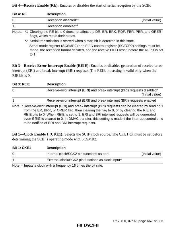
Rev. 6.0, 07/02, page 667 of 986
Bit 4—Receive Enable (RE): Enables or disables the start of serial reception by the SCIF.
Bit 4: RE Description
0 Reception disabled*1 (Initial value)
1 Reception enabled*2
Notes: *1 Clearing the RE bit to 0 does not affect the DR, ER, BRK, RDF, FER, PER, and ORERflags, which retain their states.
*2 Serial transmission is started when a start bit is detected in this state.Serial mode register (SCSMR2) and FIFO control register (SCFCR2) settings must bemade, the reception format decided, and the receive FIFO reset, before the RE bit is setto 1.
Bit 3—Receive Error Interrupt Enable (REIE): Enables or disables generation of receive-errorinterrupt (ERI) and break interrupt (BRI) requests. The REIE bit setting is valid only when theRIE bit is 0.
Bit 3: REIE Description
0 Receive-error interrupt (ERI) and break interrupt (BRI) requests disabled*(Initial value)
1 Receive-error interrupt (ERI) and break interrupt (BRI) requests enabled
Note: * Receive-error interrupt (ERI) and break interrupt (BRI) requests can be cleared by reading 1from the ER, BRK, or ORER flag, then clearing the flag to 0, or by clearing the RIE andREIE bits to 0. When REIE is set to 1, ERI and BRI interrupt requests will be generatedeven if RIE is cleared to 0. In DMAC transfer, this setting is made if the interrupt controller isto be notified of ERI and BRI interrupt requests.
Bit 1—Clock Enable 1 (CKE1): Selects the SCIF clock source. The CKE1 bit must be set beforedetermining the SCIF’s operating mode with SCSMR2.
Bit 1: CKE1 Description
0 Internal clock/SCK2 pin functions as port (Initial value)
1 External clock/SCK2 pin functions as clock input*
Note: * Inputs a clock with a frequency 16 times the bit rate.

Rev. 6.0, 07/02, page 668 of 986
16.2.7 Serial Status Register (SCFSR2)
Bit: 15 14 13 12 11 10 9 8
PER3 PER2 PER1 PER0 FER3 FER2 FER1 FER0
Initial value: 0 0 0 0 0 0 0 0
R/W: R R R R R R R R
Bit: 7 6 5 4 3 2 1 0
ER TEND TDFE BRK FER PER RDF DR
Initial value: 0 1 1 0 0 0 0 0
R/W: R/(W)* R/(W)* R/(W)* R/(W)* R R R/(W)* R/(W)*
Note: * Only 0 can be written, to clear the flag.
SCFSR2 is a 16-bit register. The lower 8 bits consist of status flags that indicate the operatingstatus of the SCIF, and the upper 8 bits indicate the number of receive errors in the data in thereceive FIFO register.
SCFSR2 can be read or written to by the CPU at all times. However, 1 cannot be written to flagsER, TEND, TDFE, BRK, RDF, and DR. Also note that in order to clear these flags they must beread as 1 beforehand. The FER flag and PER flag are read-only flags and cannot be modified.
SCFSR2 is initialized to H'0060 by a power-on reset or manual reset. It is not initialized instandby mode or in the module standby state.
Bits 15 to 12—Number of Parity Errors (PER3–PER0): These bits indicate the number of databytes in which a parity error occurred in the receive data stored in SCFRDR2.
After the ER bit in SCFSR2 is set, the value indicated by bits 15 to 12 is the number of data bytesin which a parity error occurred.
If all 16 bytes of receive data in SCFRDR2 have parity errors, the value indicated by bits PER3 toPER0 will be 0.
Bits 11 to 8—Number of Framing Errors (FER3–FER0): These bits indicate the number ofdata bytes in which a framing error occurred in the receive data stored in SCFRDR2.
After the ER bit in SCFSR2 is set, the value indicated by bits 11 to 8 is the number of data bytes inwhich a framing error occurred.
If all 16 bytes of receive data in SCFRDR2 have framing errors, the value indicated by bits FER3to FER0 will be 0.

Rev. 6.0, 07/02, page 669 of 986
Bit 7—Receive Error (ER): Indicates that a framing error or parity error occurred duringreception.*
Note: * The ER flag is not affected and retains its previous state when the RE bit in SCSCR2 iscleared to 0. When a receive error occurs, the receive data is still transferred to SCFRDR2,and reception continues.The FER and PER bits in SCFSR2 can be used to determine whether there is a receiveerror that is to be from SCFRDR2.
Bit 7: ER Description
0 No framing error or parity error occurred during reception (Initial value)
[Clearing conditions]
• Power-on reset or manual reset
• When 0 is written to ER after reading ER = 1
1 A framing error or parity error occurred during reception
[Setting conditions]
• When the SCIF checks whether the stop bit at the end of the receivedata is 1 when reception ends, and the stop bit is 0*
• When, in reception, the number of 1-bits in the receive data plus theparity bit does not match the parity setting (even or odd) specified by theO/E bit in SCSMR2
Note: * In 2-stop-bit mode, only the first stop bit is checked for a value of 1; the second stop bit isnot checked.

Rev. 6.0, 07/02, page 670 of 986
Bit 6—Transmit End (TEND): Indicates that there is no valid data in SCFTDR2 when the lastbit of the transmit character is sent, and transmission has been ended.
Bit 6: TEND Description
0 Transmission is in progress
[Clearing conditions]
• When transmit data is written to SCFTDR2, and 0 is written to TENDafter reading TEND = 1
• When data is written to SCFTDR2 by the DMAC
1 Transmission has been ended (Initial value)
[Setting conditions]
• Power-on reset or manual reset
• When the TE bit in SCSCR2 is 0
• When there is no transmit data in SCFTDR2 on transmission of the lastbit of a 1-byte serial transmit character

Rev. 6.0, 07/02, page 671 of 986
Bit 5—Transmit FIFO Data Empty (TDFE): Indicates that data has been transferred fromSCFTDR2 to SCTSR2, the number of data bytes in SCFTDR2 has fallen to or below the transmittrigger data number set by bits TTRG1 and TTRG0 in the FIFO control register (SCFCR2), andnew transmit data can be written to SCFTDR2.
Bit 5: TDFE Description
0 A number of transmit data bytes exceeding the transmit trigger set numberhave been written to SCFTDR2
[Clearing conditions]
• When transmit data exceeding the transmit trigger set number is writtento SCFTDR2 after reading TDFE = 1, and 0 is written to TDFE
• When transmit data exceeding the transmit trigger set number is writtento SCFTDR2 by the DMAC
1 The number of transmit data bytes in SCFTDR2 does not exceed thetransmit trigger set number (Initial value)
[Setting conditions]
• Power-on reset or manual reset
• When the number of SCFTDR2 transmit data bytes falls to or below thetransmit trigger set number as the result of a transmit operation*
Note: * As SCFTDR2 is a 16-byte FIFO register, the maximum number of bytes that can be writtenwhen TDFE = 1 is 16 - (transmit trigger set number). Data written in excess of this will beignored.The number of data bytes in SCFTDR2 is indicated by the upper bits of SCFDR2.
Bit 4—Break Detect (BRK): Indicates that a receive data break signal has been detected.
Bit 4: BRK Description
0 A break signal has not been received (Initial value)
[Clearing conditions]
• Power-on reset or manual reset
• When 0 is written to BRK after reading BRK = 1
1 A break signal has been received*
[Setting condition]
When data with a framing error is received, followed by the space “0” level(low level ) for at least one frame length
Note: * When a break is detected, the receive data (H'00) following detection is not transferred toSCFRDR2. When the break ends and the receive signal returns to mark “1”, receive datatransfer is resumed.

Rev. 6.0, 07/02, page 672 of 986
Bit 3—Framing Error (FER): Indicates whether or not a framing error has been found in thedata that is to be read next from SCFRDR2.
Bit 3: FER Description
0 There is no framing error that is to be read from SCFRDR2 (Initial value)
[Clearing conditions]
• Power-on reset or manual reset
• When there is no framing error in the data that is to be read next fromSCFRDR2
1 There is a framing error that is to be read from SCFRDR2
[Setting condition]
When there is a framing error in the data that is to be read next fromSCFRDR2
Bit 2—Parity Error (PER): Indicates whether or not a parity error has been found in the data thatis to be read next from SCFRDR2.
Bit 2: PER Description
0 There is no parity error that is to be read from SCFRDR2(Initial value)
[Clearing conditions]
• Power-on reset or manual reset
• When there is no parity error in the data that is to be read next fromSCFRDR2
1 There is a parity error in the receive data that is to be read from SCFRDR2
[Setting condition]
When there is a parity error in the data that is to be read next fromSCFRDR2

Rev. 6.0, 07/02, page 673 of 986
Bit 1—Receive FIFO Data Full (RDF): Indicates that the received data has been transferredfrom SCRSR2 to SCFRDR2, and the number of receive data bytes in SCFRDR2 is equal to orgreater than the receive trigger number set by bits RTRG1 and RTRG0 in the FIFO controlregister (SCFCR2).
Bit 1: RDF Description
0 The number of receive data bytes in SCFRDR2 is less than the receivetrigger set number (Initial value)
[Clearing conditions]
• Power-on reset or manual reset
• When SCFRDR2 is read until the number of receive data bytes inSCFRDR2 falls below the receive trigger set number after reading RDF= 1, and 0 is written to RDF
• When SCFRDR2 is read by the DMAC until the number of receive databytes in SCFRDR2 falls below the receive trigger set number
1 The number of receive data bytes in SCFRDR2 is equal to or greater thanthe receive trigger set number
[Setting condition]
When SCFRDR2 contains at least the receive trigger set number of receivedata bytes*
Note: * SCFRDR2 is a 16-byte FIFO register. When RDF = 1, at least the receive trigger setnumber of data bytes can be read. If all the data in SCFRDR2 is read and another read isperformed, the data value will be undefined. The number of receive data bytes in SCFRDR2is indicated by the lower bits of SCFDR2.

Rev. 6.0, 07/02, page 674 of 986
Bit 0—Receive Data Ready (DR): Indicates that there are fewer than the receive trigger setnumber of data bytes in SCFRDR2, and no further data has arrived for at least 15 etu after the stopbit of the last data received.
Bit 0: DR Description
0 Reception is in progress or has ended normally and there is no receive dataleft in SCFRDR2 (Initial value)
[Clearing conditions]
• Power-on reset or manual reset
• When all the receive data in SCFRDR2 has been read after reading DR= 1, and 0 is written to DR
• When all the receive data in SCFRDR2 has been read by the DMAC
1 No further receive data has arrived
[Setting condition]
When SCFRDR2 contains fewer than the receive trigger set number ofreceive data bytes, and no further data has arrived for at least 15 etu afterthe stop bit of the last data received*
Note: * Equivalent to 1.5 frames with an 8-bit, 1-stop-bit format.
etu: Elementary time unit (time for transfer of 1 bit)
16.2.8 Bit Rate Register (SCBRR2)
Bit: 7 6 5 4 3 2 1 0
Initial value: 1 1 1 1 1 1 1 1
R/W: R/W R/W R/W R/W R/W R/W R/W R/W
SCBRR2 is an 8-bit register that sets the serial transfer bit rate in accordance with the baud rategenerator operating clock selected by bits CKS1 and CKS0 in SCSMR2.
SCBRR2 can be read or written to by the CPU at all times.
SCBRR2 is initialized to H'FF by a power-on reset or manual reset. It is not initialized in standbymode or in the module standby state.

Rev. 6.0, 07/02, page 675 of 986
The SCBRR2 setting is found from the following equation.
Asynchronous mode:
N = × 106 – 164 × 22n–1 × B
φP
Where B: Bit rate (bits/s)N: SCBRR2 setting for baud rate generator (0 ≤ N ≤ 255)Pφ: Peripheral module operating frequency (MHz)n: Baud rate generator input clock (n = 0 to 3)
(See the table below for the relation between n and the clock.)
SCSMR2 Setting
n Clock CKS1 CKS0
0 Pφ 0 0
1 Pφ/4 0 1
2 Pφ/16 1 0
3 Pφ/64 1 1
The bit rate error in asynchronous mode is found from the following equation:
Error (%) = – 1 × 100P × 106
(N + 1) × B × 64 × 22n–1φ
16.2.9 FIFO Control Register (SCFCR2)
Bit: 15 14 13 12 11 10 9 8
— — — — — RSTRG2* RSTRG1* RSTRG0*
Initial value: 0 0 0 0 0 0 0 0
R/W: R R R R R R/W R/W R/W
Bit: 7 6 5 4 3 2 1 0
RTRG1 RTRG0 TTRG1 TTRG0 MCE TFRST RFRST LOOP
Initial value: 0 0 0 0 0 0 0 0
R/W: R/W R/W R/W R/W R/W R/W R/W R/W
Note: * Reserved bit in the SH7750.

Rev. 6.0, 07/02, page 676 of 986
SCFCR2 performs data count resetting and trigger data number setting for the transmit and receiveFIFO registers, and also contains a loopback test enable bit.
SCFCR2 can be read or written to by the CPU at all times.
SCFCR2 is initialized to H'0000 by a power-on reset or manual reset. It is not initialized instandby mode or in the module standby state.
Bits 15 to 11—Reserved: These bits are always read as 0, and should only be written with 0.
Bits 10 to 8 (SH7750)—Reserved: These bits are always read as 0, and should only be writtenwith 0.
Bits 10 to 8 (SH7750S, SH7750R)—RTS2RTS2RTS2RTS2 Output Active Trigger (RSTRG2, RSTG1, andRSTG0): These bits output the high level to the RTS2 signal when the number of received datastored in the receive FIFO data register (SCFRDR2) exceeds the trigger number, as shown in thetable below.
Bit 10: RSTRG2 Bit 9: RSTRG1 Bit 8: RSTRG0 RTS2RTS2RTS2RTS2 Output Active Trigger
0 15 (Initial value)0
1 1
0 4
0
1
1 6
0 80
1 10
0 12
1
1
1 14
Bits 7 and 6—Receive FIFO Data Number Trigger (RTRG1, RTRG0): These bits are used toset the number of receive data bytes that sets the receive data full (RDF) flag in the serial statusregister (SCFSR2).
The RDF flag is set when the number of receive data bytes in SCFRDR2 is equal to or greater thanthe trigger set number shown in the following table.
Bit 7: RTRG1 Bit 6: RTRG0 Receive Trigger Number
0 0 1 (Initial value)
1 4
1 0 8
1 14

Rev. 6.0, 07/02, page 677 of 986
Bits 5 and 4—Transmit FIFO Data Number Trigger (TTRG1, TTRG0): These bits are usedto set the number of remaining transmit data bytes that sets the transmit FIFO data register empty(TDFE) flag in the serial status register (SCFSR2). The TDFE flag is set when the number oftransmit data bytes in SCFTDR2 is equal to or less than the trigger set number shown in thefollowing table.
Bit 5: TTRG1 Bit 4: TTRG0 Transmit Trigger Number
0 0 8 (8) (Initial value)
1 4 (12)
1 0 2 (14)
1 1 (15)
Note: Figures in parentheses are the number of empty bytes in SCFTDR2 when the flag is set.
Bit 3—Modem Control Enable (MCE): Enables the CTS2 and RTS2 modem control signals.
Bit 3: MCE Description
0 Modem signals disabled* (Initial value)
1 Modem signals enabled
Note: *CTS2 is fixed at active-0 regardless of the input value, and RTS2 output is also fixed at 0.
Bit 2—Transmit FIFO Data Register Reset (TFRST): Invalidates the transmit data in thetransmit FIFO data register and resets it to the empty state.
Bit 2: TFRST Description
0 Reset operation disabled* (Initial value)
1 Reset operation enabled
Note: * A reset operation is performed in the event of a power-on reset or manual reset.
Bit 1—Receive FIFO Data Register Reset (RFRST): Invalidates the receive data in the receiveFIFO data register and resets it to the empty state.
Bit 1: RFRST Description
0 Reset operation disabled* (Initial value)
1 Reset operation enabled
Note: * A reset operation is performed in the event of a power-on reset or manual reset.

Rev. 6.0, 07/02, page 678 of 986
Bit 0—Loopback Test (LOOP): Internally connects the transmit output pin (TxD2) and receiveinput pin (RxD2), and the RTS2 pin and CTS2 pin, enabling loopback testing.
Bit 0: LOOP Description
0 Loopback test disabled (Initial value)
1 Loopback test enabled
16.2.10 FIFO Data Count Register (SCFDR2)
SCFDR2 is a 16-bit register that indicates the number of data bytes stored in SCFTDR2 andSCFRDR2.
The upper 8 bits show the number of transmit data bytes in SCFTDR2, and the lower 8 bits showthe number of receive data bytes in SCFRDR2.
SCFDR2 can be read by the CPU at all times.
Bit: 15 14 13 12 11 10 9 8
— — — T4 T3 T2 T1 T0
Initial value: 0 0 0 0 0 0 0 0
R/W: R R R R R R R R
These bits show the number of untransmitted data bytes in SCFTDR2. A value of H'00 indicatesthat there is no transmit data, and a value of H'10 indicates that SCFTDR2 is full of transmit data.
Bit: 7 6 5 4 3 2 1 0
— — — R4 R3 R2 R1 R0
Initial value: 0 0 0 0 0 0 0 0
R/W: R R R R R R R R
These bits show the number of receive data bytes in SCFRDR2. A value of H'00 indicates thatthere is no receive data, and a value of H'10 indicates that SCFRDR2 is full of receive data.

Rev. 6.0, 07/02, page 679 of 986
16.2.11 Serial Port Register (SCSPTR2)
Bit: 15 14 13 12 11 10 9 8
— — — — — — — —
Initial value: 0 0 0 0 0 0 0 0
R/W: R R R R R R R R
Bit: 7 6 5 4 3 2 1 0
RTSIO RTSDT CTSIO CTSDT — — SPB2IO SPB2DT
Initial value: 0 — 0 — 0 0 0 —
R/W: R/W R/W R/W R/W R R R/W R/W
SCSPTR2 is a 16-bit readable/writable register that controls input/output and data for the port pinsmultiplexed with the serial communication interface (SCIF) pins. Input data can be read from theRxD2 pin, output data written to the TxD2 pin, and breaks in serial transmission/receptioncontrolled, by means of bits 1 and 0. Data can be read from, and output data written to, the CTS2pin by means of bits 5 and 4. Data can be read from, and output data written to, the RTS2 pin bymeans of bits 6 and 7.
SCSPTR2 can be read or written to by the CPU at all times. All SCSPTR2 bits except bits 6, 4,and 0 are initialized to 0 by a power-on reset or manual reset; the value of bits 6, 4, and 0 isundefined. SCSPTR2 is not initialized in standby mode or in the module standby state.
Bits 15 to 8—Reserved: These bits are always read as 0, and should only be written with 0.
Bit 7—Serial Port RTS Port I/O (RTSIO): Specifies the serial port RTS2 pin input/outputcondition. When the RTS2 pin is actually set as a port output pin and outputs the value set by theRTSDT bit, the MCE bit in SCFCR2 should be cleared to 0.
Bit 7: RTSIO Description
0 RTSDT bit value is not output to RTS2 pin (Initial value)
1 RTSDT bit value is output to RTS2 pin

Rev. 6.0, 07/02, page 680 of 986
Bit 6—Serial Port RTS Port Data (RTSDT): Specifies the serial port RTS2 pin input/outputdata. Input or output is specified by the RTSIO bit (see the description of bit 7, RTSIO, fordetails). In output mode, the RTSDT bit value is output to the RTS2 pin. The RTS2 pin value isread from the RTSDT bit regardless of the value of the RTSIO bit. The initial value of this bitafter a power-on reset or manual reset is undefined.
Bit 6: RTSDT Description
0 Input/output data is low-level
1 Input/output data is high-level
Bit 5—Serial Port CTS Port I/O (CTSIO): Specifies the serial port CTS2 pin input/outputcondition. When the CTS2 pin is actually set as a port output pin and outputs the value set by theCTSDT bit, the MCE bit in SCFCR2 should be cleared to 0.
Bit 5: CTSIO Description
0 CTSDT bit value is not output to CTS2 pin (Initial value)
1 CTSDT bit value is output to CTS2 pin
Bit 4—Serial Port CTS Port Data (CTSDT): Specifies the serial port CTS2 pin input/outputdata. Input or output is specified by the CTSIO bit (see the description of bit 5, CTSIO, fordetails). In output mode, the CTSDT bit value is output to the CTS2 pin. The CTS2 pin value isread from the CTSDT bit regardless of the value of the CTSIO bit. The initial value of this bitafter a power-on reset or manual reset is undefined.
Bit 4: CTSDT Description
0 Input/output data is low-level
1 Input/output data is high-level
Bits 3 and 2—Reserved: These bits are always read as 0, and should only be written with 0.
Bit 1—Serial Port Break I/O (SPB2IO): Specifies the serial port TxD2 pin output condition.When the TxD2 pin is actually set as a port output pin and outputs the value set by the SPB2DTbit, the TE bit in SCSCR2 should be cleared to 0.
Bit 1: SPB2IO Description
0 SPB2DT bit value is not output to the TxD2 pin (Initial value)
1 SPB2DT bit value is output to the TxD2 pin

Rev. 6.0, 07/02, page 681 of 986
Bit 0—Serial Port Break Data (SPB2DT): Specifies the serial port RxD2 pin input data andTxD2 pin output data. The TxD2 pin output condition is specified by the SPB2IO bit (see thedescription of bit 1, SPB2IO, for details). When the TxD2 pin is designated as an output, the valueof the SPB2DT bit is output to the TxD2 pin. The RxD2 pin value is read from the SPB2DT bitregardless of the value of the SPB2IO bit. The initial value of this bit after a power-on reset ormanual reset is undefined.
Bit 0: SPB2DT Description
0 Input/output data is low-level
1 Input/output data is high-level
SCIF I/O port block diagrams are shown in figures 16.2 to 16.5.
Reset
Internal data bus
SPTRW
D7
D6
SCIF
RQ DRTSIO
C
Reset
Mode setting register
SPTRR
SPTRW
RQ DRTSDT
C
MD8/
SPTRW: Write to SPTRSPTRR: Read SPTR
Note: * The pin function is designated as modem control by the MCE bit in SCFCR2.
Modem control enable signal*
signal
Figure 16.2 MD8/RTS2RTS2RTS2RTS2 Pin

Rev. 6.0, 07/02, page 682 of 986
Reset
Internal data bus
SPTRW
D5
D4
SCIF
RQ DCTSIO
C
Reset
SPTRR
SPTRW
RQ DCTSDT
C
SPTRW: Write to SPTRSPTRR: Read SPTR
Note: * The pin function is designated as modem control by the MCE bit in SCFCR2.
Modem control enable signal*
signal
Figure 16.3 CTS2CTS2CTS2CTS2 Pin

Rev. 6.0, 07/02, page 683 of 986
Reset
Internal data bus
SPTRW
Mode setting register
SCIF
RQ D
D1
D0
SPB2IOC
Reset
SPTRW
RQ DSPB2DT
C
MD1/TxD2
SPTRW: Write to SPTR
Transmit enable signal
Serial transmit data
Figure 16.4 MD1/TxD2 Pin
Internal data bus
Mode setting register
SCIFMD2/RxD2
SPTRR
D0
Serial receive data
SPTRR: Read SPTR
Figure 16.5 MD2/RxD2 Pin

Rev. 6.0, 07/02, page 684 of 986
16.2.12 Line Status Register (SCLSR2)
Bit: 15 14 13 12 11 10 9 8
— — — — — — — —
Initial value: 0 0 0 0 0 0 0 0
R/W: R R R R R R R R
Bit: 7 6 5 4 3 2 1 0
— — — — — — — ORER
Initial value: 0 0 0 0 0 0 0 0
R/W: R R R R R R R (R/W)*
Note: * Only 0 can be written, to clear the flag.
Bits 15 to 1—Reserved: These bits are always read as 0, and should only be written with 0.
Bit 0—Overrun Error (ORER): Indicates that an overrun error occurred during reception,causing abnormal termination.
Bit 0: ORER Description
0 Reception in progress, or reception has ended normally*1 (Initial value)
[Clearing conditions]
• Power-on reset or manual reset
• When 0 is written to ORER after reading ORER = 1
1 An overrun error occurred during reception*2
[Setting condition]
When the next serial reception is completed while the receive FIFO is full
Notes: *1 The ORER flag is not affected and retains its previous state when the RE bit inSCSCR2 is cleared to 0.
*2 The receive data prior to the overrun error is retained in SCFRDR2, and the datareceived subsequently is lost. Serial reception cannot be continued while the ORER flagis set to 1.

Rev. 6.0, 07/02, page 685 of 986
16.3 Operation
16.3.1 Overview
The SCIF can carry out serial communication in asynchronous mode, in which synchronization isachieved character by character. See section 15.3.2, Operation in Asynchronous Mode, for details.
Sixteen-stage FIFO buffers are provided for both transmission and reception, reducing the CPUoverhead and enabling fast, continuous communication to be performed. RTS2 and CTS2 signalsare also provided as modem control signals.
The transmission format is selected using the serial mode register (SCSMR2), as shown in table16.3. The SCIF clock source is determined by the CKE1 bit in the serial control register(SCSCR2), as shown in table 16.4.
• Data length: Choice of 7 or 8 bits
• Choice of parity addition and addition of 1 or 2 stop bits (the combination of these parametersdetermines the transfer format and character length)
• Detection of framing errors, parity errors, receive-FIFO-data-full state, overrun errors, receive-data-ready state, and breaks, during reception
• Indication of the number of data bytes stored in the transmit and receive FIFO registers
• Choice of internal or external clock as SCIF clock source
When internal clock is selected: The SCIF operates on the baud rate generator clock, and canoutput a clock with a frequency of 16 times the bit rate.
When external clock is selected: A clock with a frequency of 16 times the bit rate must beinput (the on-chip baud rate generator is not used).
Table 16.3 SCSMR2 Settings for Serial Transfer Format Selection
SCSMR2 Settings SCIF Transfer Format
Bit 6:CHR
Bit 5:PE
Bit 3:STOP Mode
DataLength
MultiprocessorBit
ParityBit
Stop BitLength
0 0 0 Asynchronous mode 8-bit data No No 1 bit
1 2 bits
1 0 Yes 1 bit
1 2 bits
1 0 0 7-bit data No 1 bit
1 2 bits
1 0 Yes 1 bit
1 2 bits

Rev. 6.0, 07/02, page 686 of 986
Table 16.4 SCSCR2 Settings for SCIF Clock Source Selection
SCSCR2 Setting SCIF Transmit/Receive Clock
Bit 1: CKE1 Mode Clock Source SCK2 Pin Function
0 Asynchronous mode Internal SCIF does not use SCK2 pin
1 External Inputs clock with frequency of 16times the bit rate
16.3.2 Serial Operation
Transmit/Receive Format
Table 16.5 shows the transmit/receive formats that can be used. Any of 8 transfer formats can beselected according to the SCSMR2 settings.
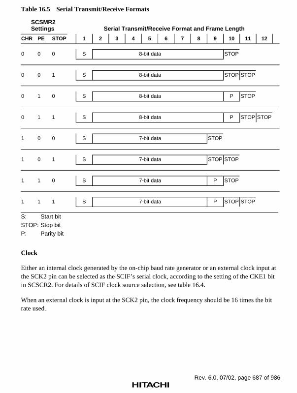
Rev. 6.0, 07/02, page 687 of 986
Table 16.5 Serial Transmit/Receive Formats
SCSMR2Settings Serial Transmit/Receive Format and Frame Length
CHR PE STOP 1 2 3 4 5 6 7 8 9 10 11 12
0 0 0 S 8-bit data STOP
0 0 1 S 8-bit data STOP STOP
0 1 0 S 8-bit data P STOP
0 1 1 S 8-bit data P STOP STOP
1 0 0 S 7-bit data STOP
1 0 1 S 7-bit data STOP STOP
1 1 0 S 7-bit data P STOP
1 1 1 S 7-bit data P STOP STOP
S: Start bitSTOP: Stop bitP: Parity bit
Clock
Either an internal clock generated by the on-chip baud rate generator or an external clock input atthe SCK2 pin can be selected as the SCIF’s serial clock, according to the setting of the CKE1 bitin SCSCR2. For details of SCIF clock source selection, see table 16.4.
When an external clock is input at the SCK2 pin, the clock frequency should be 16 times the bitrate used.

Rev. 6.0, 07/02, page 688 of 986
Data Transfer Operations
SCIF Initialization: Before transmitting and receiving data, it is necessary to clear the TE and REbits in SCSCR2 to 0, then initialize the SCIF as described below.
When the transfer format, etc., is changed, the TE and RE bits must be cleared to 0 before makingthe change using the following procedure. When the TE bit is cleared to 0, SCTSR2 is initialized.Note that clearing the TE and RE bits to 0 does not change the contents of SCFSR2, SCFTDR2, orSCFRDR2. The TE bit should be cleared to 0 after all transmit data has been sent and the TENDflag in SCFSR2 has been set. TEND can also be cleared to 0 during transmission, but the databeing transmitted will go to the mark state after the clearance. Before setting TE again to starttransmission, the TFRST bit in SCFCR2 should first be set to 1 to reset SCFTDR2.
When an external clock is used the clock should not be stopped during operation, includinginitialization, since operation will be unreliable in this case.
Figure 16.6 shows a sample SCIF initialization flowchart.

Rev. 6.0, 07/02, page 689 of 986
Initialization
Clear TE and RE bitsin SCSCR2 to 0
Set TFRST and RFRST bitsin SCFCR2 to 1
Set CKE1 bit in SCSCR2 (leaving TE and RE bits
cleared to 0)
Set transmit/receive formatin SCSMR2
Set value in SCBRR2
1-bit interval elapsed?
Set RTRG1–0, TTRG1–0,and MCE bits in SCFCR2
Clear TFRST and RFRST bits to 0
Set TE and RE bitsin SCSCR2 to 1,
and set RIE, TIE, and REIE bits
End
Wait
No
Yes
1. Set the clock selection in SCSCR2.
Be sure to clear bits RIE and TIE, and bits TE and RE, to 0.
2. Set the transmit/receive format in SCSMR2.
3. Write a value corresponding to the bit rate into SCBRR2. (Not necessary if an external clock is used.)
4. Wait at least one bit interval, then set the TE bit or RE bit in SCSCR2 to 1. Also set the RIE, REIE, and TIE bits.
Setting the TE and RE bits enables the TxD2 and RxD2 pins to be used. When transmitting, the SCIF will go to the mark state; when receiving, it will go to the idle state, waiting for a start bit.
Figure 16.6 Sample SCIF Initialization Flowchart

Rev. 6.0, 07/02, page 690 of 986
Serial Data Transmission: Figure 16.7 shows a sample flowchart for serial transmission.
Use the following procedure for serial data transmission after enabling the SCIF for transmission.
Start of transmission
Read TDFE flag in SCFSR2
TDFE = 1?
Write transmit data (16 - transmittrigger set number) to SCFTDR2,read 1 from TDFE flag and TENDflag in SCFSR2, then clear to 0
All data transmitted?
Read TEND flag in SCFSR2
TEND = 1?
Break output?
Clear SPB2DT to 0 andset SPB2IO to 1
Clear TE bit in SCSCR2 to 0
End of transmission
No
Yes
No
Yes
No
Yes
No
Yes
1. SCIF status check and transmit data write:
Read SCFSR2 and check that the TDFE flag is set to 1, then write transmit data to SCFTDR2, read 1 from the TDFE and TEND flags, then clear these flags to 0.
The number of transmit data bytes that can be written is 16 - (transmit trigger set number).
2. Serial transmission continuation procedure:
To continue serial transmission, read 1 from the TDFE flag to confirm that writing is possible, then write data to SCFTDR2, and then clear the TDFE flag to 0.
3. Break output at the end of serial transmission:
To output a break in serial transmission, clear the SPB2DT bit to 0 and set the SPB2IO bit to 1 in SCSPTR2, then clear the TE bit in SCSCR2 to 0.
In steps 1 and 2, it is possible to ascertain the number of data bytes that can be written from the number of transmit data bytes in SCFTDR2 indicated by the upper 8 bits of SCFDR2.
Figure 16.7 Sample Serial Transmission Flowchart

Rev. 6.0, 07/02, page 691 of 986
In serial transmission, the SCIF operates as described below.
1. When data is written into SCFTDR2, the SCIF transfers the data from SCFTDR2 to SCTSR2and starts transmitting. Confirm that the TDFE flag in the serial status register (SCFSR2) is setto 1 before writing transmit data to SCFTDR2. The number of data bytes that can be written isat least 16 - transmit trigger setting.
2. When data is transferred from SCFTDR2 to SCTSR2 and transmission is started, consecutivetransmit operations are performed until there is no transmit data left in SCFTDR2. When thenumber of transmit data bytes in SCFTDR2 falls to or below the transmit trigger number set inthe FIFO control register (SCFCR2), the TDFE flag is set. If the TIE bit in SCSCR2 is set to 1at this time, a transmit-FIFO-data-empty interrupt (TXI) request is generated.
The serial transmit data is sent from the TxD2 pin in the following order.
a. Start bit: One 0-bit is output.
b. Transmit data: 8-bit or 7-bit data is output in LSB-first order.
c. Parity bit: One parity bit (even or odd parity) is output. (A format in which a parity bit isnot output can also be selected.)
d. Stop bit(s): One or two 1-bits (stop bits) are output.
e. Mark state: 1 is output continuously until the start bit that starts the next transmission issent.
3. The SCIF checks the SCFTDR2 transmit data at the timing for sending the stop bit. If data ispresent, the data is transferred from SCFTDR2 to SCTSR2, the stop bit is sent, and then serialtransmission of the next frame is started.
If there is no transmit data, the TEND flag in SCFSR2 is set to 1, the stop bit is sent, and thenthe line goes to the mark state in which 1 is output.
Figure 16.8 shows an example of the operation for transmission in asynchronous mode.

Rev. 6.0, 07/02, page 692 of 986
1
0 D0 D1 D7 0/1 1 0 D0 D1 D7 0/1 1
1
TDFE
TEND
Serial data
Start bit
Data Parity bit
Stop bit
Start bit
Idle state (mark state)
Data Parity bit
Stop bit
TXI interrupt request
Data written to SCFTDR2 and TDFE flag read as 1 then cleared to 0 by TXI interrupt handler
One frame
TXI interrupt request
Figure 16.8 Example of Transmit Operation(Example with 8-Bit Data, Parity, One Stop Bit)
4. When modem control is enabled, transmission can be stopped and restarted in accordance withthe CTS2 input value. When CTS2 is set to 1, if transmission is in progress, the line goes to themark state after transmission of one frame. When CTS2 is set to 0, the next transmit data isoutput starting from the start bit.
Figure 16.9 shows an example of the operation when modem control is used.
Serial dataTxD2
0 D0 D1 D7 0/1 01 D0 D1 D7 0/1
CTS2
Drive high before stop bit
Startbit
Paritybit
Stopbit
Startbit
Figure 16.9 Example of Operation Using Modem Control (CTS2CTS2CTS2CTS2)

Rev. 6.0, 07/02, page 693 of 986
Serial Data Reception: Figure 16.10 shows a sample flowchart for serial reception.
Use the following procedure for serial data reception after enabling the SCIF for reception.
Start of reception
Read ER, DR, BRK flags inSCFSR2 and ORER
flag in SCLSR2
ER or DR or BRK or ORER= 1?
Read RDF flag in SCFSR2
RDF = 1?
Read receive data inSCFRDR2, and clear RDF
flag in SCFSR2 to 0
All data received?
Clear RE bit in SCSCR2 to 0
End of reception
Yes
No
Yes
Yes
No
No
Error handling
1. Receive error handling and break detection: Read the DR, ER, and BRK flags in SCFSR2, and the ORER flag in SCLSR2, to identify any error, perform the appropriate error handling, then clear the DR, ER, BRK, and ORER flags to 0. In the case of a framing error, a break can also be detected by reading the value of the RxD2 pin.
2. SCIF status check and receive data read : Read SCFSR2 and check that RDF = 1, then read the receive data in SCFRDR2, read 1 from the RDF flag, and then clear the RDF flag to 0. The transition of the RDF flag from 0 to 1 can also be identified by an RXI interrupt.
3. Serial reception continuation procedure: To continue serial reception, read at least the receive trigger set number of receive data bytes from SCFRDR2, read 1 from the RDF flag, then clear the RDF flag to 0. The number of receive data bytes in SCFRDR2 can be ascertained by reading the lower bits of SCFDR2.
Figure 16.10 Sample Serial Reception Flowchart (1)

Rev. 6.0, 07/02, page 694 of 986
Error handling
Receive error handling
ER = 1?
BRK = 1?
Break handling
DR = 1?
Read receive data in SCFRDR2
Clear DR, ER, BRK flags in SCFSR2,
and ORER flag in SCLSR2, to 0
End
Yes
Yes
Yes
No
Overrun error handling
ORER = 1?
Yes
No
No
No
1. Whether a framing error or parity error has occurred that is to be read from SCFRDR2 can be ascertained from the FER and PER bits in SCFSR2.
2. When a break signal is received, receive data is not transferred to SCFRDR2 while the BRK flag is set. However, note that the last data in SCFRDR2 is H'00 (the break data in which a framing error occurred is stored).
Figure 16.10 Sample Serial Reception Flowchart (2)

Rev. 6.0, 07/02, page 695 of 986
In serial reception, the SCIF operates as described below.
1. The SCIF monitors the transmission line, and if a 0 start bit is detected, performs internalsynchronization and starts reception.
2. The received data is stored in SCRSR2 in LSB-to-MSB order.
3. The parity bit and stop bit are received.
After receiving these bits, the SCIF carries out the following checks.
a. Stop bit check: The SCIF checks whether the stop bit is 1. If there are two stop bits, onlythe first is checked.
b. The SCIF checks whether receive data can be transferred from the receive shift register(SCRSR2) to SCFRDR2.
c. Overrun error check: The SCIF checks that the ORER flag is 0, indicating that no overrunerror has occurred.
d. Break check: The SCIF checks that the BRK flag is 0, indicating that the break state is notset.
If b, c, and d checks are passed, the receive data is stored in SCFRDR2.
Note: Reception continues when parity error, framing error occurs.
4. If the RIE bit in SCSCR2 is set to 1 when the RDF or DR flag changes to 1, a receive-FIFO-data-full interrupt (RXI) request is generated.
If the RIE bit or REIE bit in SCSCR2 is set to 1 when the ER flag changes to 1, a receive-errorinterrupt (ERI) request is generated.
If the RIE bit or REIE bit in SCSCR2 is set to 1 when the BRK or ORER flag changes to 1, abreak reception interrupt (BRI) request is generated.
Figure 16.11 shows an example of the operation for reception in asynchronous mode.

Rev. 6.0, 07/02, page 696 of 986
1
0 D0 D1 D7 0/1 1 0 D0 D1 D7 0/1 0/10
RDF
FER
Serial data
Start bit
Data Parity bit
Stop bit
Start bit
Data Parity bit
Stop bit
RXI interrupt request
One frame
Data read and RDF flag read as 1 then cleared to 0 by RXI interrupt handler
ERI interrupt request generated by receive error
Figure 16.11 Example of SCIF Receive Operation(Example with 8-Bit Data, Parity, One Stop Bit)
5. When modem control is enabled, the RTS2 signal is output when SCFRDR2 is empty. WhenRTS2 is 0, reception is possible.
SH7750: When RTS2 is 1, this indicates that SCFRDR2 contains 15 or morebytes of data.
SH7750S, SH7750R: When RTS2 is 1, this indicates that SCFRDR2 contains a number ofdata bytes equal to or greater than the RTS2 output active trigger setnumber. The RTS2 output active trigger value is specified by bits 10 to8 in the FIFO control register (SCFCR2), described in section 16.2.9,FIFO control register (SCFCR2).
RTS2 also becomes 1 when bit 4 (RE) in SCSCR2 is 0.
Figure 16.12 shows an example of the operation when modem control is used.
D0 D1 D2 D7 0/1 1 00Serial data
RxD2
Start bit
Parity bit
Stopbit
Start bit
Figure 16.12 Example of Operation Using Modem Control (RTS2RTS2RTS2RTS2)

Rev. 6.0, 07/02, page 697 of 986
16.4 SCIF Interrupt Sources and the DMAC
The SCIF has four interrupt sources: transmit-FIFO-data-empty interrupt (TXI) request, receive-error interrupt (ERI) request, receive-FIFO-data-full interrupt (RXI) request, and break interrupt(BRI) request.
Table 16.6 shows the interrupt sources and their order of priority. The interrupt sources areenabled or disabled by means of the TIE, RIE, and REIE bits in SCSCR2. A separate interruptrequest is sent to the interrupt controller for each of these interrupt sources.
When transmission/reception is carried out using the DMAC, output of interrupt requests to theinterrupt controller can be inhibited by clearing the RIE bit in SCSCR2 to 0. By setting the REIEbit to 1 while the RIE bit is cleared to 0, it is possible to output ERI and BRI interrupt requests, butnot RXI interrupt requests.
When the TDFE flag in the serial status register (SCFSR2) is set to 1, a transmit-FIFO-data-emptyrequest is generated separately from the interrupt request. A transmit-FIFO-data-empty requestcan activate the DMAC to perform data transfer.
When the RDF flag or DR flag in SCFSR2 is set to 1, a receive-FIFO-data-full request isgenerated separately from the interrupt request. A receive-FIFO-data-full request can activate theDMAC to perform data transfer.
When using the DMAC for transmission/reception, set and enable the DMAC before making theSCIF settings. See section 14, Direct Memory Access Controller (DMAC), for details of theDMAC setting procedure.
When the BRK flag in SCFSR2 or the ORER flag in the line status register (SCLSR2) is set to 1, aBRI interrupt request is generated.
The TXI interrupt indicates that transmit data can be written, and the RXI interrupt indicates thatthere is receive data in SCFRDR2.
Table 16.6 SCIF Interrupt Sources
InterruptSource Description
DMACActivation
Priority onReset Release
ERI Interrupt initiated by receive error flag (ER) Not possible High
RXI Interrupt initiated by receive FIFO data full flag(RDF) or receive data ready flag (DR)
Possible
BRI Interrupt initiated by break flag (BRK) or overrunerror flag (ORER)
Not possible
TXI Interrupt initiated by transmit FIFO data emptyflag (TDFE)
Possible Low

Rev. 6.0, 07/02, page 698 of 986
See section 5, Exceptions, for priorities and the relationship with non-SCIF interrupts.
16.5 Usage Notes
Note the following when using the SCIF.
SCFTDR2 Writing and the TDFE Flag: The TDFE flag in the serial status register (SCFSR2) isset when the number of transmit data bytes written in the transmit FIFO data register (SCFTDR2)has fallen to or below the transmit trigger number set by bits TTRG1 and TTRG0 in the FIFOcontrol register (SCFCR2). After TDFE is set, transmit data up to the number of empty bytes inSCFTDR2 can be written, allowing efficient continuous transmission.
However, if the number of data bytes written in SCFTDR2 is equal to or less than the transmittrigger number, the TDFE flag will be set to 1 again after being read as 1 and cleared to 0. TDFEclearing should therefore be carried out when SCFTDR2 contains more than the transmit triggernumber of transmit data bytes.
The number of transmit data bytes in SCFTDR2 can be found from the upper 8 bits of the FIFOdata count register (SCFDR2).
SCFRDR2 Reading and the RDF Flag: The RDF flag in the serial status register (SCFSR2) isset when the number of receive data bytes in the receive FIFO data register (SCFRDR2) hasbecome equal to or greater than the receive trigger number set by bits RTRG1 and RTRG0 in theFIFO control register (SCFCR2). After RDF is set, receive data equivalent to the trigger numbercan be read from SCFRDR2, allowing efficient continuous reception.
However, if the number of data bytes in SCFRDR2 is equal to or greater than the trigger number,the RDF flag will be set to 1 again if it is cleared to 0. RDF should therefore be cleared to 0 afterbeing read as 1 after all the receive data has been read.
The number of receive data bytes in SCFRDR2 can be found from the lower 8 bits of the FIFOdata count register (SCFDR2).
Break Detection and Processing: Break signals can be detected by reading the RxD2 pin directlywhen a framing error (FER) is detected. In the break state the input from the RxD2 pin consists ofall 0s, so the FER flag is set and the parity error flag (PER) may also be set.
Although the SCIF stops transferring receive data to SCFRDR2 after receiving a break, the receiveoperation continues.
Sending a Break Signal: The input/output condition and level of the TxD2 pin are determined bybits SPB2IO and SPB2DT in the serial port register (SCSPTR2). This feature can be used to senda break signal.

Rev. 6.0, 07/02, page 699 of 986
After the serial transmitter is initialized, the TxD2 pin function is not selected and the value of theSPB2DT bit substitutes for the mark state until the TE bit is set to 1 (i.e. transmission is enabled).The SPB2IO and SPB2DT bits should therefore be set to 1 (designating output and high level)beforehand.
To send a break signal during serial transmission, clear the SPB2DT bit to 0 (designating lowlevel), then clear the TE bit to 0 (halting transmission). When the TE bit is cleared to 0, thetransmitter is initialized, regardless of its current state, and 0 is output from the TxD2 pin.
Receive Data Sampling Timing and Receive Margin: The SCIF operates on a base clock with afrequency of 16 times the transfer rate. In reception, the SCIF synchronizes internally with the fallof the start bit, which it samples on the base clock. Receive data is latched at the rising edge of theeighth base clock pulse. The timing is shown in figure 16.13.
0 1 2 3 4 5 6 7 8 9 10 11 12 13 14 15 0 1 2 3 4 5 6 7 8 9 10 11 12 13 14 15 0 1 2 3 4 5
D0 D1
16 clocks
8 clocks
Base clock
Receive data(RxD2)
Start bit
–7.5 clocks +7.5 clocks
Synchronizationsampling timing
Data samplingtiming
Figure 16.13 Receive Data Sampling Timing in Asynchronous Mode
The receive margin in asynchronous mode can therefore be expressed as shown in equation (1).
M = (0.5 – ) – (L – 0.5) F – (1 + F) × 100%1
2N| D – 0.5 |
N ...................... (1)
M: Receive margin (%)N: Ratio of clock frequency to bit rate (N = 16)D: Clock duty cycle (D = 0 to 1.0)L: Frame length (L = 9 to 12)F: Absolute deviation of clock frequency

Rev. 6.0, 07/02, page 700 of 986
From equation (1), if F = 0 and D = 0.5, the receive margin is 46.875%, as given by equation (2).
When D = 0.5 and F = 0:
M = (0.5 – 1 / (2 × 16) ) × 100% = 46.875% ............................................... (2)
This is a theoretical value. A reasonable margin to allow in system designs is 20% to 30%.
SCK2/MRESETMRESETMRESETMRESET: As the manual reset pin is multiplexed with the SCK2 pin, a manual reset mustnot be executed while the SCIF is operating in external clock mode.
When Using the DMAC: When using the DMAC for transmission/reception, inhibit output ofRXI and TXI interrupt requests to the interrupt controller. If interrupt request output is enabled,interrupt requests to the interrupt controller will be cleared by the DMAC without regard to theinterrupt handler.
Serial Ports: Note that, when the SCIF pin value is read using a serial port, the value read will bethe value two peripheral clock cycles earlier.
Overrun Error Flag (SH7750): SCIF overrun error flag is not set in the case that overrun errorand flaming error occurred simultaneously in receiving data, that means 17th byte data whichoverrun was accompanying with flaming error. In such case, only SCFSR2. ER flag which showsoccurrence of flaming error is set. Receive FIFO stores data received before the overrun and doesnot store (i. e. lose) overrun data. SCIF has no bit which corresponds to SCFSR2. FER for the lostdata.
In addition to the overrun error handling software routine, exception handler should check co-occurrence of overrun error when a flaming error is occurred and when a co-occurrence is found,it should handle also overrun error (When (i) a overrun error solely occurred withoutaccompanying with other receive error and (ii) when a parity error is accompanied with overrunerror, usual overrun error handling can be used. Overrun error handling should rather be doneprimarily).

Rev. 6.0, 07/02, page 701 of 986
Read receive FIFO
Last data?
No
No
Yes
Yes
Normal error handling
Error handling
No
Yes
Overrun error handling +
framing error handling
Framing error occurrenceFlow chart:
When flaming error (SCFSR.ER=1) is occurred, bit7 to
bit0 should be read out from SCFDR2. If bit7 to bit0
equals H'10, contents of the receive FIFO should be
read. When the data received last is not accompanied
with flaming error (SCFSR2.FER=0) both overrun error
handling and flaming error handling shoud be
conducted.
Bits 7 to 0 in SCFDR2 = H'10?
PER or FER bit in SCFSR2 set to 1?
Figure 16.14 Overrun Error Flag

Rev. 6.0, 07/02, page 702 of 986

Rev. 6.0, 07/02, page 703 of 986
Section 17 Smart Card Interface
17.1 Overview
The subset of the IC card (smart card) interface conforming to ISO/IEC7816-3 (IdentificationCard) is supported as a serial communication interface (SCI) extension function.
Switching between the normal serial communication interface and the smart card interface iscarried out by means of a register setting.
17.1.1 Features
Features of the smart card interface are listed below.
• Asynchronous mode
Data length: 8 bits
Parity bit generation and checking
Transmission of error signal (parity error) in receive mode
Error signal detection and automatic data retransmission in transmit mode
Direct convention and inverse convention both supported
• On-chip baud rate generator allows any bit rate to be selected
• Three interrupt sources
There are three interrupt sources—transmit-data-empty, receive-data-full, and transmit/receiveerror—that can issue requests independently.
The transmit-data-empty interrupt and receive-data-full interrupt can activate the DMAcontroller (DMAC) to execute data transfer.

Rev. 6.0, 07/02, page 704 of 986
17.1.2 Block Diagram
Figure 17.1 shows a block diagram of the smart card interface.
Module data bus
SCRDR1
SCRSR1RxD
TxD
SCK
SCTDR1
SCTSR1
SCSCMR1SCSSR1SCSCR1
SCBRR1
Parity generation
Parity check
Transmission/reception
control
Baud rategenerator
Clock
External clock
Pφ
Pφ/4
Pφ/16
Pφ/64
TXIRXIERI
SCI
Bus
inte
rfac
e Internal data bus
SCSMR1
SCSCMR1: Smart card mode registerSCRSR1: Receive shift registerSCRDR1: Receive data registerSCTSR1: Transmit shift registerSCTDR1: Transmit data registerSCSMR1: Serial mode registerSCSCR1: Serial control registerSCSSR1: Serial status registerSCBRR1: Bit rate registerSCSPTR1: Serial port register
SCSPTR1
Figure 17.1 Block Diagram of Smart Card Interface

Rev. 6.0, 07/02, page 705 of 986
17.1.3 Pin Configuration
Table 17.1 shows the smart card interface pin configuration.
Table 17.1 Smart Card Interface Pins
Pin Name Abbreviation I/O Function
Serial clock pin MD0/SCK I/O Clock input/output
Receive data pin RxD Input Receive data input
Transmit data pin MD7/TxD Output Transmit data output
17.1.4 Register Configuration
The smart card interface has the internal registers shown in table 17.2. Details of the SCBRR1,SCTDR1, SCRDR1, and SCSPTR1 registers are the same as for the normal SCI function: see theregister descriptions in section 15, Serial Communication Interface (SCI).
With the exception of the serial port register, the smart card interface registers are initialized instandby mode and in the module standby state as well as by a power-on reset or manual reset.When recovering from standby mode or the module standby state, the registers must be set again.
Table 17.2 Smart Card Interface Registers
Name Abbreviation R/WInitialValue P4 Address
Area 7Address
AccessSize
Serial mode register SCSMR1 R/W H'00 H'FFE00000 H'1FE00000 8
Bit rate register SCBRR1 R/W H'FF H'FFE00004 H'1FE00004 8
Serial control register SCSCR1 R/W H'00 H'FFE00008 H'1FE00008 8
Transmit data register SCTDR1 R/W H'FF H'FFE0000C H'1FE0000C 8
Serial status register SCSSR1 R/(W)*1 H'84 H'FFE00010 H'1FE00010 8
Receive data register SCRDR1 R H'00 H'FFE00014 H'1FE00014 8
Smart card moderegister
SCSCMR1 R/W H'00 H'FFE00018 H'1FE00018 8
Serial port register SCSPTR1 R/W H'00*2 H'FFE0001C H'1FE0001C 8
Notes: *1 Only 0 can be written, to clear flags.*2 The value of bits 2 and 0 is undefined.

Rev. 6.0, 07/02, page 706 of 986
17.2 Register Descriptions
Only registers that have been added, and bit functions that have been modified, for the smart cardinterface are described here.
17.2.1 Smart Card Mode Register (SCSCMR1)
SCSCMR1 is an 8-bit readable/writable register that selects the smart card interface function.SCSCMR1 is initialized to H'00 by a power-on reset or manual reset, in standby mode, and in themodule standby state.
Bit: 7 6 5 4 3 2 1 0
— — — — SDIR SINV — SMIF
Initial value: — — — — 0 0 — 0
R/W: — — — — R/W R/W — R/W
Bits 7 to 4 and 1—Reserved: These bits are always read as 0, and should only be written with 0.
Bit 3—Smart Card Data Transfer Direction (SDIR): Selects the serial/parallel conversionformat.
Bit 3: SDIR Description
0 SCTDR1 contents are transmitted LSB-first (Initial value)
Receive data is stored in SCRDR1 LSB-first
1 SCTDR1 contents are transmitted MSB-first
Receive data is stored in SCRDR1 MSB-first
Bit 2—Smart Card Data Invert (SINV): Specifies inversion of the data logic level. Thisfunction is used together with the bit 3 function for communication with an inverse conventioncard. The SINV bit does not affect the logic level of the parity bit. For parity-related settingprocedures, see section 17.3.4, Register Settings.
Bit 2: SINV Description
0 SCTDR1 contents are transmitted as they are (Initial value)
Receive data is stored in SCRDR1 as it is
1 SCTDR1 contents are inverted before being transmitted
Receive data is stored in SCRDR1 in inverted form

Rev. 6.0, 07/02, page 707 of 986
Bit 0—Smart Card Interface Mode Select (SMIF): Enables or disables the smart card interfacefunction.
Bit 0: SMIF Description
0 Smart card interface function is disabled (Initial value)
1 Smart card interface function is enabled
17.2.2 Serial Mode Register (SCSMR1)
Bit 7 of SCSMR1 has a different function in smart card interface mode.
Bit: 7 6 5 4 3 2 1 0
GM(C/A) CHR PE O/E STOP MP CKS1 CKS0
Initial value: 0 0 0 0 0 0 0 0
R/W: R/W R/W R/W R/W R/W R/W R/W R/W
Bit 7—GSM Mode (GM): Sets the smart card interface function to GSM mode.
With the normal smart card interface, this bit is cleared to 0. Setting this bit to 1 selects GSMmode, an additional mode for controlling the timing for setting the TEND flag that indicatescompletion of transmission, and the type of clock output used. The details of the additional clockoutput control mode are specified by the CKE1 and CKE0 bits in the serial control register(SCSCR1). In GSM mode, the pulse width is guaranteed when SCK start/stop specifications aremade by CKE1 and CKE0.
Bit 7: GM Description
0 Normal smart card interface mode operation (Initial value)
• The TEND flag is set 12.5 etu after the beginning of the start bit
• Clock output on/off control only
1 GSM mode smart card interface mode operation
• The TEND flag is set 11.0 etu after the beginning of the start bit
• Clock output on/off and fixed-high/fixed-low control (set in SCSCR1)
Note: etu: Elementary time unit (time for transfer of 1 bit)
Bits 6 to 0: Operate in the same way as for the normal SCI. See section 15, Serial CommunicationInterface (SCI), for details. With the smart card interface, the following settings should be used:CHR = 0, PE = 1, STOP = 1, MP = 0.

Rev. 6.0, 07/02, page 708 of 986
17.2.3 Serial Control Register (SCSCR1)
Bits 1 and 0 of SCSCR1 have a different function in smart card interface mode.
Bit: 7 6 5 4 3 2 1 0
TIE RIE TE RE — — CKE1 CKE0
Initial value: 0 0 0 0 0 0 0 0
R/W: R/W R/W R/W R/W R/W R/W R/W R/W
Bits 7 to 4: Operate in the same way as for the normal SCI. See section 15, Serial CommunicationInterface (SCI), for details.
Bits 3 and 2—Reserved: Not used with the smart card interface.
Bits 1 and 0—Clock Enable 1 and 0 (CKE1, CKE0): These bits specify the function of the SCKpin. In smart card interface mode, an internal clock is always used as the clock source. In smartcard interface mode, it is possible to specify a fixed high level or fixed low level for the clockoutput, in addition to the usual switching between enabling and disabling of the clock output.
GM CKE1 CKE0 SCK Pin Function
0 0 0 Port I/O pin
1 Clock output as SCK output pin
1 0 Invalid setting: must not be used
1 Invalid setting: must not be used
1 0 0 Output pin with output fixed low
1 Clock output as output pin
1 0 Output pin with output fixed high
1 Clock output as output pin

Rev. 6.0, 07/02, page 709 of 986
17.2.4 Serial Status Register (SCSSR1)
Bit 4 of SCSSR1 has a different function in smart card interface mode. Coupled with this, thesetting conditions for bit 2 (TEND) are also different.
Bit: 7 6 5 4 3 2 1 0
TDRE RDRF ORER FER/ERS
PER TEND — —
Initial value: 1 0 0 0 0 1 0 0
R/W: R/(W)* R/(W)* R/(W)* R/(W)* R/(W)* R R R/W
Note: * Only 0 can be written, to clear the flag.
Bits 7 to 5: Operate in the same way as for the normal SCI. See section 15, Serial CommunicationInterface (SCI), for details.
Bit 4—Error Signal Status (ERS): In smart card interface mode, bit 4 indicates the status of theerror signal sent back from the receiving side during transmission. Framing errors are not detectedin smart card interface mode.
Bit 4: ERS Description
0 Normal reception, no error signal (Initial value)
[Clearing conditions]
• Power-on reset, manual reset, standby mode, or module standby
• When 0 is written to ERS after reading ERS = 1
1 An error signal has been sent from the receiving side indicating detection ofa parity error
[Setting condition]
• When the low level of the error signal is detected
Note: Clearing the TE bit in SCSCR1 to 0 does not affect the ERS flag, which retains its previousstate.
Bit 3—Parity Error (PER): Operates in the same way as for the normal SCI. See section 15,Serial Communication Interface (SCI), for details.

Rev. 6.0, 07/02, page 710 of 986
Bit 2—Transmit End (TEND): The setting conditions for the TEND flag are as follows.
Bit 2: TEND Description
0 Transmission in progress
[Clearing condition]
• When 0 is written to TDRE after reading TDRE = 1
1 Transmission has been ended (Initial value)
[Setting conditions]
• Power-on reset, manual reset, standby mode, or module standby
• When the TE bit in SCSCR1 is 0 and the FER/ERS bit is also 0
• When the GM bit in SCSMR1 is 0, and TDRE = 1 and FER/ERS = 0(normal transmission) 2.5 etu after transmission of a 1-byte serialcharacter
• When the GM bit in SCSMR1 is 1, and TDRE = 1 and FER/ERS = 0(normal transmission) 1.0 etu after transmission of a 1-byte serialcharacter
etu: Elementary Time Unit (time for transfer for 1 bit)
Bits 1 and 0—Reserved: Not used with the smart card interface.
17.3 Operation
17.3.1 Overview
The main functions of the smart card interface are as follows.
• One frame consists of 8-bit data plus a parity bit.
• In transmission, a guard time of at least 2 etu (elementary time unit: the time for transfer of onebit) is left between the end of the parity bit and the start of the next frame.
• If a parity error is detected during reception, a low error signal level is output for a 1-etu period10.5 etu after the start bit.
• If an error signal is detected during transmission, the same data is transmitted automaticallyafter the elapse of 2 etu or longer.
• Only asynchronous communication is supported; there is no synchronous communicationfunction.

Rev. 6.0, 07/02, page 711 of 986
17.3.2 Pin Connections
Figure 17.2 shows a schematic diagram of smart card interface related pin connections.
In communication with an IC card, since both transmission and reception are carried out on asingle data transmission line, the TxD pin and RxD pin should be connected outside the chip. Thedata transmission line should be pulled up on the VCC power supply side with a resistor.
When the clock generated on the smart card interface is used by an IC card, the SCK pin output isinput to the CLK pin of the IC card. No connection is needed if the IC card uses an internal clock.
Chip port output is used as the reset signal.
Other pins must normally be connected to the power supply or ground.
Note: If an IC card is not connected, and both TE and RE are set to 1, closedtransmission/reception is possible, enabling self-diagnosis to be carried out.
SH7750Series
Connected equipment
TxD
RxD
SCK
Px (port)
Data line
Clock line
Reset line
IO
CLK
RST
IC card
VCC
Figure 17.2 Schematic Diagram of Smart Card Interface Pin Connections

Rev. 6.0, 07/02, page 712 of 986
17.3.3 Data Format
Figure 17.3 shows the smart card interface data format. In reception in this mode, a parity check iscarried out on each frame, and if an error is detected an error signal is sent back to the transmittingside to request retransmission of the data. If an error signal is detected during transmission, thesame data is retransmitted.
Ds D0 D1 D2 D3 D4 D5 D6 D7 Dp
Ds D0 D1 D2 D3 D4 D5 D6 D7 Dp DE
Ds: Start bitD0–D7: Data bitsDp: Parity bitDE: Error signal
When there is no parity error
When a parity error occurs
Transmitting station output
Transmitting station output
Receiving station output
Figure 17.3 Smart Card Interface Data Format
The operation sequence is as follows.
1. When the data line is not in use it is in the high-impedance state, and is fixed high with a pull-up resistor.
2. The transmitting station starts transmission of one frame of data. The data frame starts with astart bit (Ds, low-level), followed by 8 data bits (D0 to D7) and a parity bit (Dp).
3. With the smart card interface, the data line then returns to the high-impedance state. The dataline is pulled high with a pull-up resistor.
4. The receiving station carries out a parity check.
If there is no parity error and the data is received normally, the receiving station waits forreception of the next data.

Rev. 6.0, 07/02, page 713 of 986
If a parity error occurs, however, the receiving station outputs an error signal (DE, low-level)to request retransmission of the data. After outputting the error signal for the prescribed lengthof time, the receiving station places the signal line in the high-impedance state again. Thesignal line is pulled high again by a pull-up resistor.
5. If the transmitting station does not receive an error signal, it proceeds to transmit the next dataframe.
If it receives an error signal, however, it returns to step 2 and retransmits the erroneous data.
17.3.4 Register Settings
Table 17.3 shows a bit map of the registers used by the smart card interface. Bits indicated as 0 or1 must be set to the value shown. The setting of other bits is described below.
Table 17.3 Smart Card Interface Register Settings
Bit
Register Bit 7 Bit 6 Bit 5 Bit 4 Bit 3 Bit 2 Bit 1 Bit 0
SCSMR1 GM 0 1 O/E 1 0 CKS1 CKS0
SCBRR1 BRR7 BRR6 BRR5 BRR4 BRR3 BRR2 BRR1 BRR0
SCSCR1 TIE RIE TE RE 0 0 CKE1 CKE0
SCTDR1 TDR7 TDR6 TDR5 TDR4 TDR3 TDR2 TDR1 TDR0
SCSSR1 TDRE RDRF ORER FER/ERS PER TEND 0 0
SCRDR1 RDR7 RDR6 RDR5 RDR4 RDR3 RDR2 RDR1 RDR0
SCSCMR1 — — — — SDIR SINV — SMIF
SCSPTR1 EIO — — — SPB1IO SPB1DT SPB0IO SPB0DT
Note: A dash indicates an unused bit.
Serial Mode Register (SCSMR1) Settings: The GM bit is used to select the timing of TEND flagsetting, and, together with the CKE1 and CKE0 bits in the serial control register (SCSCR1), toselect the clock output state.
The O/E bit is cleared to 0 if the IC card is of the direct convention type, and set to 1 if of theinverse convention type.
Bits CKS1 and CKS0 select the clock source of the on-chip baud rate generator. See section17.3.5, Clock.

Rev. 6.0, 07/02, page 714 of 986
I/O data
TXI(TEND interrupt)
etu: Elementary Time Unit (time for transfer for 1 bit)
Guardtime
Ds Da Db Dc Dd De Df Dg Dh Dp DE
12.5 etu
11.0 etu
GM = 0
GM = 1
Figure 17.4 TEND Generation Timing
Bit Rate Register (SCBRR1) Setting: SCBRR1 is used to set the bit rate. See section 17.3.5,Clock, for the method of calculating the value to be set.
Serial Control Register (SCSCR1) Settings: The function of the TIE, RIE, TE, and RE bits isthe same as for the normal SCI. See section 15, Serial Communication Interface (SCI), for details.
The CKE1 and CKE0 bits specify the clock output state. See section 17.3.5, Clock, for details.
Smart Card Mode Register (SCSCMR1) Settings: The SDIR bit and SINV bit are both clearedto 0 if the IC card is of the direct convention type, and both set to 1 if of the inverse conventiontype.
The SMIF bit is set to 1 when the smart card interface is used.
Figure 17.5 shows examples of register settings and the waveform of the start character for the twotypes of IC card (direct convention and inverse convention).
With the direct convention type, the logic 1 level corresponds to state Z and the logic 0 level tostate A, and transfer is performed in LSB-first order. The start character data in this case is H'3B.The parity bit is 1 since even parity is stipulated for the smart card.
With the inverse convention type, the logic 1 level corresponds to state A and the logic 0 level tostate Z, and transfer is performed in MSB-first order. The start character data in this case is H'3F.The parity bit is 0, corresponding to state Z, since even parity is stipulated for the smart card.
Inversion specified by the SINV bit applies only to the data bits, D7 to D0. For parity bitinversion, the O/E bit in SCSMR1 is set to odd parity mode. (This applies to both transmission andreception).

Rev. 6.0, 07/02, page 715 of 986
(Z)
(a) Direct convention (SDIR = SINV = O/ = 0)
(b) Inverse convention (SDIR = SINV = O/ = 1)
A Z Z A Z Z Z A A Z (Z) State
Ds D0 D1 D2 D3 D4 D5 D6 D7 Dp
(Z) A Z Z A A A A A A Z (Z) State
Ds D7 D6 D5 D4 D3 D2 D1 D0 Dp
Figure 17.5 Sample Start Character Waveforms
17.3.5 Clock
Only an internal clock generated by the on-chip baud rate generator can be used as thetransmit/receive clock for the smart card interface. The bit rate is set with the bit rate register(SCBRR1) and the CKS1 and CKS0 bits in the serial mode register (SCSMR1). The equation forcalculating the bit rate is shown below. Table 17.5 shows some sample bit rates.
If clock output is selected with CKE0 set to 1, a clock with a frequency of 372 times the bit rate isoutput from the SCK pin.
B = × 106
1488 × 22n–1 × (N + 1)φP
Where: N = Value set in SCBRR1 (0 ≤ N ≤ 255)B = Bit rate (bits/s)Pφ = Peripheral module operating frequency (MHz)n = 0 to 3 (See table 17.4)
Table 17.4 Values of n and Corresponding CKS1 and CKS0 Settings
n CKS1 CKS0
0 0 0
1 0 1
2 1 0
3 1 1

Rev. 6.0, 07/02, page 716 of 986
Table 17.5 Examples of Bit Rate B (bits/s) for Various SCBRR1 Settings (When n = 0)
Pφφφφ (MHz)
N 7.1424 10.00 10.7136 14.2848 25.0 33.0 50.0
0 9600.0 13440.9 14400.0 19200.0 33602.2 44354.8 67204.3
1 4800.0 6720.4 7200.0 9600.0 16801.1 22177.4 33602.2
2 3200.0 4480.3 4800.0 6400.0 11200.7 14784.9 22401.4
Note: Bit rates are rounded to one decimal place.
The method of calculating the value to be set in the bit rate register (SCBRR1) from the peripheralmodule operating frequency and bit rate is shown below. Here, N is an integer in the range 0 ≤ N ≤255, and the smaller error is specified.
N = × 106 – 11488 × 22n–1 × B
φP
Table 17.6 Examples of SCBRR1 Settings for Bit Rate B (bits/s) (When n = 0)
Pφφφφ (MHz)
7.1424 10.00 10.7136 14.2848 25.00 33.00 50.00
Bits/s N Error N Error N Error N Error N Error N Error N Error
9600 0 0.00 1 30.00 1 25.00 1 8.99 3 14.27 4 8.22 6 0.01
Table 17.7 Maximum Bit Rate at Various Frequencies (Smart Card Interface Mode)
Pφφφφ (MHz) Maximum Bit Rate (bits/s) N n
7.1424 19200 0 0
10.00 26882 0 0
10.7136 28800 0 0
16.00 43010 0 0
20.00 53763 0 0
25.0 67204 0 0
30.0 80645 0 0
33.0 88710 0 0
50.0 67204 0 0

Rev. 6.0, 07/02, page 717 of 986
The bit rate error is given by the following equation:
Error (%) =1488 × 22n–1 × B × (N + 1)
× 106 – 1 × 100Pφ
Table 17.8 shows the relationship between the smart card interface transmit/receive clock registersettings and the output state.
Table 17.8 Register Settings and SCK Pin State
Register Values SCK Pin
Setting SMIF GM CKE1 CKE0 Output State
1*1 1 0 0 0 Port Determined by setting of SPB1IOand SPB1DT bits in SCSPTR1
1 0 0 1 SCK (serial clock) output state
2*2 1 1 0 0 Low output Low-level output state
1 1 0 1 SCK (serial clock) output state
3*2 1 1 1 0 High output High-level output state
1 1 1 1 SCK (serial clock) output state
Notes: *1 The SCK output state changes as soon as the CKE0 bit setting is changed.Clear the CKE1 bit to 0.
*2 Stopping and starting the clock by changing the CKE0 bit setting does not affect theclock duty cycle.
Port value Width is undefined
CKE1 value Specifiedwidth
SCK
SCK
(a) When GM = 0
(b) When GM = 1
Width is undefined
Specifiedwidth
Port value
CKE1 value
Figure 17.6 Difference in Clock Output According to GM Bit Setting

Rev. 6.0, 07/02, page 718 of 986
17.3.6 Data Transmit/Receive Operations
Initialization: Before transmitting and receiving data, the smart card interface must be initializedas described below. Initialization is also necessary when switching from transmit mode to receivemode, or vice versa. Figure 17.7 shows a sample initialization processing flowchart.
1. Clear the TE and RE bits in the serial control register (SCSCR1) to 0.
2. Clear error flags FER/ERS, PER, and ORER in the serial status register (SCSSR1) to 0.
3. Set the GM bit, parity bit (O/E), and baud rate generator select bits (CKS1 and CKS0) in theserial mode register (SCSMR1). Clear the CHR and MP bits to 0, and set the STOP and PEbits to 1.
4. Set the SMIF, SDIR, and SINV bits in the smart card mode register (SCSCMR1).
When the SMIF bit is set to 1, the TxD pin and RxD pin both go to the high-impedance state.
5. Set the value corresponding to the bit rate in the bit rate register (SCBRR1).
6. Set the clock source select bits (CKE1 and CKE0) in SCSCR1. Clear the TIE, RIE, TE, RE,MPIE, and TEIE bits to 0.
If the CKE0 bit is set to 1, the clock is output from the SCK pin.
7. Wait at least one bit interval, then set the TIE, RIE, TE, and RE bits in SCSCR1. Do not set theTE bit and RE bit at the same time, except for self-diagnosis.

Rev. 6.0, 07/02, page 719 of 986
Initialization
Clear TE and RE bits in SCSCR1 to 0
Clear FER/ERS, PER, andORER flags in SCSCR1 to 0
In SCSMR1, set parity in O/ bit,clock in CKS1 and CKS0 bits,
and set GM
Set SMIF, SDIR, and SINV bitsin SCSCMR1
Set value in SCBRR1
In SCSCR1, set clock in CKE1and CKE0 bits, and clear TIE,
RIE, TE, RE, MPIE, andTEIE bits to 0.
1-bit interval elapsed?
Set TIE, RIE, TE, and RE bitsin SCSCR1
End
Wait
No
Yes
1
2
3
4
5
6
7
Figure 17.7 Sample Initialization Flowchart

Rev. 6.0, 07/02, page 720 of 986
Serial Data Transmission: As data transmission in smart card mode involves error signalsampling and retransmission processing, the processing procedure is different from that for thenormal SCI. Figure 17.8 shows a sample transmission processing flowchart.
1. Perform smart card interface mode initialization as described in Initialization above.
2. Check that the FER/ERS error flag in SCSSR1 is cleared to 0.
3. Repeat steps 2 and 3 until it can be confirmed that the TEND flag in SCSSR1 is set to 1.
4. Write the transmit data to SCTDR1, clear the TDRE flag to 0, and perform the transmitoperation. The TEND flag is cleared to 0.
5. To continue transmitting data, go back to step 2.
6. To end transmission, clear the TE bit to 0.
With the above processing, interrupt handling is possible.
If transmission ends and the TEND flag is set to 1 while the TIE bit is set to 1 and interruptrequests are enabled, a transmit-data-empty interrupt (TXI) request will be generated. If an erroroccurs in transmission and the ERS flag is set to 1 while the RIE bit is set to 1 and interruptrequests are enabled, a transmit/receive-error interrupt (ERI) request will be generated. SeeInterrupt Operation in section 17.3.6 below for details.

Rev. 6.0, 07/02, page 721 of 986
Start
Initialization
Start of transmission
Write transmit data to SCTDR1,and clear TDRE flag
in SCSSR1 to 0
FER/ERS = 0?
TEND = 1?
All data transmitted?
FER/ERS = 0?
TEND = 1?
Clear TE bit in SCSCR1 to 0
End of transmission
Error handling
Error handling
No
Yes
Yes
Yes
Yes
No
Yes
No
No
No
1
2
3
4
5
6
Figure 17.8 Sample Transmission Processing Flowchart

Rev. 6.0, 07/02, page 722 of 986
Serial Data Reception: Data reception in smart card mode uses the same processing procedure asfor the normal SCI. Figure 17.9 shows a sample reception processing flowchart.
1. Perform smart card interface mode initialization as described in Initialization above.
2. Check that the ORER flag and PER flag in SCSSR1 are cleared to 0. If either is set, performthe appropriate receive error handling, then clear both the ORER and the PER flag to 0.
3. Repeat steps 2 and 3 until it can be confirmed that the RDRF flag is set to 1.
4. Read the receive data from SCRDR1.
5. To continue receiving data, clear the RDRF flag to 0 and go back to step 2.
6. To end reception, clear the RE bit to 0.
With the above processing, interrupt handling is possible.
If reception ends and the RDRF flag is set to 1 while the RIE bit is set to 1 and interrupt requestsare enabled, a receive-data-full interrupt (RXI) request will be generated. If an error occurs inreception and either the ORER flag or the PER flag is set to 1, a transmit/receive-error interrupt(ERI) request will be generated.
See Interrupt Operation in section 17.3.6 below for details.
If a parity error occurs during reception and the PER flag is set to 1, the received data is stilltransferred to SCRDR1, and therefore this data can be read.

Rev. 6.0, 07/02, page 723 of 986
Start
Initialization
Start of reception
Read receive data fromSCRDR1 and clear RDRF flag
in SCSSR1 to 0
ORER = 0 and PER = 0?
RDRF = 1?
All data received?
Clear RE bit in SCSCR1 to 0
End of reception
Error handling
No
Yes
Yes
Yes
No
No
1
2
3
4
5
6
Figure 17.9 Sample Reception Processing Flowchart
Mode Switching Operation: When switching from receive mode to transmit mode, first confirmthat the receive operation has been completed, then start from initialization, clearing RE to 0 andsetting TE to 1. The RDRF flag or the PER and ORER flags can be used to check that the receiveoperation has been completed.
When switching from transmit mode to receive mode, first confirm that the transmit operation hasbeen completed, then start from initialization, clearing TE to 0 and setting RE to 1. The TENDflag can be used to check that the transmit operation has been completed.

Rev. 6.0, 07/02, page 724 of 986
Interrupt Operation: There are three interrupt sources in smart card interface mode, generatingtransmit-data-empty interrupt (TXI) requests, transmit/receive-error interrupt (ERI) requests, andreceive-data-full interrupt (RXI) requests. The transmit-end interrupt (TEI) request cannot be usedin this mode.
When the TEND flag in SCSSR1 is set to 1, a TXI interrupt request is generated.
When the RDRF flag in SCSSR1 is set to 1, an RXI interrupt request is generated.
When any of flags ORER, PER, and FER/ERS in SCSSR1 is set to 1, an ERI interrupt request isgenerated. The relationship between the operating states and interrupt sources is shown in table17.9.
Table 17.9 Smart Card Mode Operating States and Interrupt Sources
Operating State Flag Mask Bit Interrupt Source
Transmit mode Normal operation TEND TIE TXI
Error FER/ERS RIE ERI
Receive mode Normal operation RDRF RIE RXI
Error PER, ORER RIE ERI
Data Transfer Operation by DMAC: In smart card mode, as with the normal SCI, transfer canbe carried out using the DMAC. In a transmit operation, when the TEND flag in SCSSR1 is set to1, a TXI interrupt is requested. If the TXI request is designated beforehand as a DMAC activationsource, the DMAC will be activated by the TXI request, and transfer of the transmit data will becarried out. The TEND flag is automatically cleared to 0 when data transfer is performed by theDMAC. In the event of an error, the SCI retransmits the same data automatically. The TEND flagremains cleared to 0 during this time, and the DMAC is not activated. Thus, the number of bytesspecified by the SCI and DMAC are transmitted automatically, including retransmission followingan error. However, the ERS flag is not cleared automatically when an error occurs, and thereforethe RIE bit should be set to 1 beforehand so that an ERI request will be generated in the event ofan error, and the ERS flag will be cleared.
In a receive operation, an RXI interrupt request is generated when the RDRF flag in SCSSR1 isset to 1. If the RXI request is designated beforehand as a DMAC activation source, the DMACwill be activated by the RXI request, and transfer of the receive data will be carried out. TheRDRF flag is cleared to 0 automatically when data transfer is performed by the DMAC. If an erroroccurs, an error flag is set but the RDRF flag is not. The DMAC is not activated, but instead, anERI interrupt request is sent to the CPU. The error flag must therefore be cleared.
When performing data transfer using the DMAC, it is essential to set and enable the DMACbefore carrying out SCI settings. For details of the DMAC setting procedures, see section 14,Direct Memory Access Controller (DMAC).

Rev. 6.0, 07/02, page 725 of 986
17.4 Usage Notes
The following points should be noted when using the SCI as a smart card interface.
(1) Receive Data Sampling Timing and Receive Margin
In asynchronous mode, the SCI operates on a base clock with a frequency of 372 times the transferrate. In reception, the SCI synchronizes internally with the fall of the start bit, which it samples onthe base clock. Receive data is latched at the rising edge of the 186th base clock pulse. The timingis shown in figure 17.10.
0 185 371 0 185 371 0Base clock
372 clocks
186 clocks
Start bit D0 D1
Receive data(RxD)
Synchronizationsampling timing
Data samplingtiming
Figure 17.10 Receive Data Sampling Timing in Smart Card Mode
The receive margin in smart card mode can therefore be expressed as shown in the followingequation.
M = (0.5 – ) – (L – 0.5) F – (1 + F) × 100%1
2N| D – 0.5 |
N
M: Receive margin (%)N: Ratio of clock frequency to bit rate (N = 372)D: Clock duty cycle (D = 0 to 1.0)L: Frame length (L =10)F: Absolute deviation of clock frequency

Rev. 6.0, 07/02, page 726 of 986
From the above equation, if F = 0 and D = 0.5, the receive margin is 49.866%, as given by thefollowing equation.
When D = 0.5 and F = 0:
M = (0.5 – 1/2 × 372) × 100% = 49.866%
(2) Retransfer Operations
Retransfer operations are performed by the SCI in receive mode and transmit mode as describedbelow.
Retransfer Operation when SCI is in Receive Mode: Figure 17.11 illustrates the retransferoperation when the SCI is in receive mode.
1. If an error is found when the received parity bit is checked, the PER bit in SCSSR1 isautomatically set to 1. If the RIE bit in SCSCR1 is enabled at this time, an ERI interruptrequest is generated. The PER bit in SCSSR1 should be cleared to 0 before the next parity bitis sampled.
2. The RDRF bit in SCSSR1 is not set for a frame in which an error has occurred.
3. If an error is found when the received parity bit is checked, the PER bit in SCSSR1 is not set to1.
4. If no error is found when the received parity bit is checked, the receive operation is judged tohave been completed normally, and the RDRF bit in SCSSR1 is automatically set to 1. If theRIE bit in SCSCR1 is enabled at this time, an RXI interrupt request is generated.
5. When a normal frame is received, the pin retains the high-impedance state at the timing forerror signal transmission.
Ds
nth transfer frame Retransferred frame Transfer frame n+1
D0D1 D2 D3 D4 D5 D6 D7 Dp(DE)
Ds DsD0 D0 D1 D1D2 D2DE D3 D3D4 D4D5 D6 D7 Dp
RDRF
PER
1
2
3
4
5
Figure 17.11 Retransfer Operation in SCI Receive Mode

Rev. 6.0, 07/02, page 727 of 986
Retransfer Operation when SCI is in Transmit Mode: Figure 17.12 illustrates the retransferoperation when the SCI is in transmit mode.
1. If an error signal is sent back from the receiving side after transmission of one frame iscompleted, the FER/ERS bit in SCSSR1 is set to 1. If the RIE bit in SCSCR1 is enabled at thistime, an ERI interrupt request is generated. The FER/ERS bit in SCSSR1 should be cleared to0 before the next parity bit is sampled.
2. The TEND bit in SCSSR1 is not set for a frame for which an error signal indicating an error isreceived.
3. If an error signal is not sent back from the receiving side, the FER/ERS bit in SCSSR1 is notset.
4. If an error signal is not sent back from the receiving side, transmission of one frame, includinga retransfer, is judged to have been completed, and the TEND bit in SCSSR1 is set to 1. If theTIE bit in SCSCR1 is enabled at this time, a TXI interrupt request is generated.
TDRE
Ds
nth transfer frame Retransferred frame Transfer frame n+1
D0D1 D2 D3 D4 D5 D6 D7 Dp(DE)
Ds DsD0 D0 D1 D1D2 D2DE D3 D3D4 D4D5 D6 D7 Dp
TEND
FER/ERS
1
2
3
4
Transfer from SCTDR1 to SCTSR1
Transfer from SCTDR1 to SCTSR1
Transfer from SCTDR1 to SCTSR1
Figure 17.12 Retransfer Operation in SCI Transmit Mode

Rev. 6.0, 07/02, page 728 of 986
(3) Standby Mode and Clock
When switching between smart card interface mode and standby mode, the following proceduresshould be used to maintain the clock duty cycle.
Switching from Smart Card Interface Mode to Standby Mode:1. Set the SBP1IO and SBP1DT bits in SCSPTR1 to the values for the fixed output state in
standby mode.
2. Write 0 to the TE and RE bits in the serial control register (SCSCR1) to stop transmit/receiveoperations. At the same time, set the CKE1 bit to the value for the fixed output state in standbymode.
3. Write 0 to the CKE0 bit in SCSCR1 to stop the clock.
4. Wait for one serial clock cycle. During this period, the duty cycle is preserved and clock outputis fixed at the specified level.
5. Write H'00 to the serial mode register (SCSMR1) and smart card mode register (SCSMR1).
6. Make the transition to the standby state.
Returning from Standby Mode to Smart Card Interface Mode:7. Clear the standby state.
8. Set the CKE1 bit in SCSCR1 to the value for the fixed output state at the start of standby (thecurrent SCK pin state).
9. Set smart card interface mode and output the clock. Clock signal generation is started with thenormal duty cycle.
Normal operation Normal operationStandby mode
1 2 3 4 5 6 7 8 9
Figure 17.13 Procedure for Stopping and Restarting the Clock

Rev. 6.0, 07/02, page 729 of 986
(4) Power-On and Clock
The following procedure should be used to secure the clock duty cycle after powering on.
1. The initial state is port input and high impedance. Use pull-up or pull-down resistors to fix thepotential.
2. Fix at the output specified by the CKE1 bit in the serial control register (SCSCR1).
3. Set the serial mode register (SCSMR1) and smart card mode register (SCSCMR1), and switchto smart card mode operation.
4. Set the CKE0 bit in SCSCR1 to 1 to start clock output.

Rev. 6.0, 07/02, page 730 of 986

Rev. 6.0, 07/02, page 731 of 986
Section 18 I/O Ports
18.1 Overview
The SH7750 Series has a 20-bit general-purpose I/O port, SCI I/O port, and SCIF I/O port.
18.1.1 Features
The features of the general-purpose I/O port are as follows:
• 20-bit I/O port with input/output direction independently specifiable for each bit
• Pull-up can be specified independently for each bit.
• Interrupt input is possible for 16 of the 20 I/O port bits.
• Use or non-use of the I/O port can be selected with the PORTEN bit in bus control register 2(BCR2).
The features of the SCI I/O port are as follows:
• Data can be output when the I/O port is designated for output and SCI enabling has not beenset. This allows break function transmission.
• The RxD pin value can be read at all times, allowing break state detection.
• SCK pin control is possible when the I/O port is designated for output and SCI enabling hasnot been set.
• The SCK pin value can be read at all times.
The features of the SCIF I/O port are as follows:
• Data can be output when the I/O port is designated for output and SCIF enabling has not beenset. This allows break function transmission.
• The RxD2 pin value can be read at all times, allowing break state detection.
• CTS2 and RTS2 pin control is possible when the I/O port is designated for output and SCIFenabling has not been set.
• The CTS2 and RTS2 pin values can be read at all times.

Rev. 6.0, 07/02, page 732 of 986
18.1.2 Block Diagrams
Figure 18.1 shows a block diagram of the 16-bit general-purpose I/O port.
PBnPUPPORTEN
DnDIR
PBnIO
0
1
PDTRW
BCK
Data input strobe
D QC
0
1
0
1
MP
XM
PX
MP
X
PTIRENn BCK
CQ
D
Pull-up resistor
Port 15 (input/output)/D47toPort 0 (input/output)/D32
Dn output data
Internal bus
Dn input dataInterruptcontroller
PORTEN 0: Port not available 1: Port availablePBnPuP 0: Pull-up 1: Pull-up offDnDIR 0: Input 1: OutputPBnIO 0: Input 1: OutputPTIRENn 0: Interrupt input disabled 1: Interrupt input enabled
Figure 18.1 16-Bit Port

Rev. 6.0, 07/02, page 733 of 986
Figure 18.2 shows a block diagram of the 4-bit general-purpose I/O port.
PBnPUP
PORTEN
DnDIR
PBnIO
0
1
PDTRW
BCK
D QC
0
1
0
1
BCK
CQ D
MP
XM
PX
MP
X
Data input strobe
Pull-up resistor
Port 19 (input/output)/D51toPort 16 (input/output)/D48
Dn output data
Internal bus
PORTEN 0: Port not available 1: Port availablePBnPuP 0: Pull-up 1: Pull-up offDnDIR 0: Input 1: OutputPBnIO 0: Input 1: Output
Dn input data
Figure 18.2 4-Bit Port

Rev. 6.0, 07/02, page 734 of 986
SCI I/O port block diagrams are shown in figures 18.3 to 18.5.
Reset
Reset
Internal data busSPTRW
SPTRW
SCI
RQ DSPB1IO
C
RQ DSPB1DT
C
SPTRR
Clock output enable signal
Serial clock output signal
Serial clock input signal
Clock input enable signal
*
MD0/SCK
Mode settingregister
SPTRW: Write to SPTRSPTRR: Read SPTR
Note: * Signals that set the SCK pin function as internal clock output or external clock input according to the CKE0 and CKE1 bits in SCSCR1 and the C/ bit in SCSMR1.
Figure 18.3 MD0/SCK Pin
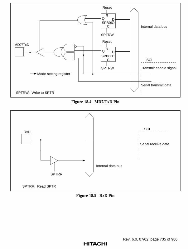
Rev. 6.0, 07/02, page 735 of 986
Reset
Internal data bus
SPTRW
SCI
RQ DSPB0IO
C
Reset
SPTRW
RQ DSPB0DT
C
MD7/TxD
Mode setting register
Transmit enable signal
Serial transmit data
SPTRW: Write to SPTR
Figure 18.4 MD7/TxD Pin
Internal data bus
SCIRxD
SPTRR
Serial receive data
SPTRR: Read SPTR
Figure 18.5 RxD Pin

Rev. 6.0, 07/02, page 736 of 986
SCIF I/O port block diagrams are shown in figures 18.6 to 18.9.
Reset
Internal data bus
SPTRW
Mode setting register
SCIF
RQ DSPB2IO
C
Reset
SPTRW
RQ DSPB2DT
C
MD1/TxD2
SPTRW: Write to SPTR
Transmit enable signal
Serial transmit data
Figure 18.6 MD1/TxD2 Pin
Internal data bus
Mode setting register
SCIFMD2/RxD2
SPTRR
Serial receive data
SPTRR: Read SPTR
Figure 18.7 MD2/RxD2 Pin

Rev. 6.0, 07/02, page 737 of 986
Reset
Internal data bus
SPTRW
SCIF
RQ DCTSIO
C
Reset
SPTRR
SPTRW
RQ DCTSDT
C
SPTRW: Write to SPTRSPTRR: Read SPTR
Note: * MCE bit in SCFCR2: signal that designates modem control as the pin function.
Modem control enable signal*
signal
Figure 18.8 CTS2CTS2CTS2CTS2 Pin

Rev. 6.0, 07/02, page 738 of 986
Reset
Internal data bus
SPTRW
SCIF
RQ DRTSIO
C
Reset
Mode setting register
SPTRR
SPTRW
RQ DRTSDT
C
MD8/
SPTRW: Write to SPTRSPTRR: Read SPTR
Note: * MCE bit in SCFCR2: signal that designates modem control as the pin function.
Modem control enable signal*
signal
Figure 18.9 MD8/RTS2RTS2RTS2RTS2 Pin

Rev. 6.0, 07/02, page 739 of 986
18.1.3 Pin Configuration
Table 18.1 shows the 20-bit general-purpose I/O port pin configuration.
Table 18.1 20-Bit General-Purpose I/O Port Pins
Pin Name Signal I/O Function
Port 19 pin PORT19/D51 I/O I/O port
Port 18 pin PORT18/D50 I/O I/O port
Port 17 pin PORT17/D49 I/O I/O port
Port 16 pin PORT16/D48 I/O I/O port
Port 15 pin PORT15/D47 I/O* I/O port / GPIO interrupt
Port 14 pin PORT14/D46 I/O* I/O port / GPIO interrupt
Port 13 pin PORT13/D45 I/O* I/O port / GPIO interrupt
Port 12 pin PORT12/D44 I/O* I/O port / GPIO interrupt
Port 11 pin PORT11/D43 I/O* I/O port / GPIO interrupt
Port 10 pin PORT10/D42 I/O* I/O port / GPIO interrupt
Port 9 pin PORT9/D41 I/O* I/O port / GPIO interrupt
Port 8 pin PORT8/D40 I/O* I/O port / GPIO interrupt
Port 7 pin PORT7/D39 I/O* I/O port / GPIO interrupt
Port 6 pin PORT6/D38 I/O* I/O port / GPIO interrupt
Port 5 pin PORT5/D37 I/O* I/O port / GPIO interrupt
Port 4 pin PORT4/D36 I/O* I/O port / GPIO interrupt
Port 3 pin PORT3/D35 I/O* I/O port / GPIO interrupt
Port 2 pin PORT2/D34 I/O* I/O port / GPIO interrupt
Port 1 pin PORT1/D33 I/O* I/O port / GPIO interrupt
Port 0 pin PORT0/D32 I/O* I/O port / GPIO interrupt
Note: * When port pins are used as GPIO interrupts, they must be set to input mode. The inputsetting can be made in the PCTRA register.

Rev. 6.0, 07/02, page 740 of 986
Table 18.2 shows the SCI I/O port pin configuration.
Table 18.2 SCI I/O Port Pins
Pin Name Abbreviation I/O Function
Serial clock pin MD0/SCK I/O Clock input/output
Receive data pin RxD Input Receive data input
Transmit data pin MD7/TxD Output Transmit data output
Note: Pins MD0/SCK and MD7/TxD function as mode input pins MD0 and MD7 after a power-onreset. They are made to function as serial pins by performing SCI operation settings withthe TE, RE, CKEI, and CKE0 bits in SCSCR1 and the C/A bit in SCSMR1. Break statetransmission and detection can be performed by means of a setting in the SCI’s SCSPTR1register.
Table 18.3 shows the SCIF I/O port pin configuration.
Table 18.3 SCIF I/O Port Pins
Pin Name Abbreviation I/O Function
Serial clock pin MRESET/SCK2 Input Clock input
Receive data pin MD2/RxD2 Input Receive data input
Transmit data pin MD1/TxD2 Output Transmit data output
Modem control pin CTS2 I/O Transmission enabled
Modem control pin MD8/RTS2 I/O Transmission request
Note: The MRESET/SCK2 pin functions as the MRESET manual reset pin when a manual reset isexecuted. The MD1/TxD2, MD2/RxD2, and MD8/RTS2 pins function as the MD1, MD2, andMD8 mode input pins after a power-on reset. These pins are made to function as serial pinsby performing SCIF operation settings with the TE and RE bits in SCSCR2 and the MCE bitin SCFCR2. Break state transmission and detection can be set in the SCIF’s SCSPTR2register.

Rev. 6.0, 07/02, page 741 of 986
18.1.4 Register Configuration
The 20-bit general-purpose I/O port, SCI I/O port, and SCIF I/O port have seven registers, asshown in table 18.4.
Table 18.4 I/O Port Registers
Name Abbreviation R/W Initial Value* P4 AddressArea 7Address
AccessSize
Port control register A PCTRA R/W H'00000000 H'FF80002C H'1F80002C 32
Port data register A PDTRA R/W Undefined H'FF800030 H'1F800030 16
Port control register B PCTRB R/W H'00000000 H'FF800040 H'1F800040 32
Port data register B PDTRB R/W Undefined H'FF800044 H'1F800044 16
GPIO interrupt controlregister
GPIOIC R/W H'00000000 H'FF800048 H'1F800048 16
Serial port register SCSPTR1 R/W Undefined H'FFE0001C H'1FE0001C 8
Serial port register SCSPTR2 R/W Undefined H'FFE80020 H'1FE80020 16
Note: * Initialized by a power-on reset.

Rev. 6.0, 07/02, page 742 of 986
18.2 Register Descriptions
18.2.1 Port Control Register A (PCTRA)
Port control register A (PCTRA) is a 32-bit readable/writable register that controls theinput/output direction and pull-up for each bit in the 16-bit port (port 15 pin to port 0 pin). As theinitial value of port data register A (PDTRA) is undefined, all the bits in the 16-bit port should beset to output with PCTRA after writing a value to the PDTRA register.
PCTRA is initialized to H'00000000 by a power-on reset. It is not initialized by a manual reset orin standby mode, and retains its contents.
Bit: 31 30 29 28 27 26 25 24
PB15PUP PB15IO PB14PUP PB14IO PB13PUP PB13IO PB12PUP PB12IO
Initial value: 0 0 0 0 0 0 0 0
R/W: R/W R/W R/W R/W R/W R/W R/W R/W
Bit: 23 22 21 20 19 18 17 16
PB11PUP PB11IO PB10PUP PB10IO PB9PUP PB9IO PB8PUP PB8IO
Initial value: 0 0 0 0 0 0 0 0
R/W: R/W R/W R/W R/W R/W R/W R/W R/W
Bit: 15 14 13 12 11 10 9 8
PB7PUP PB7IO PB6PUP PB6IO PB5PUP PB5IO PB4PUP PB4IO
Initial value: 0 0 0 0 0 0 0 0
R/W: R/W R/W R/W R/W R/W R/W R/W R/W
Bit: 7 6 5 4 3 2 1 0
PB3PUP PB3IO PB2PUP PB2IO PB1PUP PB1IO PB0PUP PB0IO
Initial value: 0 0 0 0 0 0 0 0
R/W: R/W R/W R/W R/W R/W R/W R/W R/W

Rev. 6.0, 07/02, page 743 of 986
Bit 2n + 1 (n = 0–15)—Port Pull-Up Control (PBnPUP): Specifies whether each bit in the 16-bit port is to be pulled up with a built-in resistor. Pull-up is automatically turned off for a port pinset to output by bit PBnIO.
Bit 2n + 1: PBnPUP Description
0 Bit m (m = 0–15) of 16-bit port is pulled up (Initial value)
1 Bit m (m = 0–15) of 16-bit port is not pulled up
Bit 2n (n = 0–15)—Port I/O Control (PBnIO): Specifies whether each bit in the 16-bit port is aninput or an output.
Bit 2n: PBnIO Description
0 Bit m (m = 0–15) of 16-bit port is an input (Initial value)
1 Bit m (m = 0–15) of 16-bit port is an output
18.2.2 Port Data Register A (PDTRA)
Port data register A (PDTRA) is a 16-bit readable/writable register used as a data latch for each bitin the 16-bit port. When a bit is set as an output, the value written to the PDTRA register is outputfrom the external pin. When a value is read from the PDTRA register while a bit is set as an input,the external pin value sampled on the external bus clock is read. When a bit is set as an output, thevalue written to the PDTRA register is read.
PDTRA is not initialized by a power-on or manual reset, or in standby mode, and retains itscontents.
Bit: 15 14 13 12 11 10 9 8
PB15DT PB14DT PB13DT PB12DT PB11DT PB10DT PB9DT PB8DT
Initial value: — — — — — — — —
R/W: R/W R/W R/W R/W R/W R/W R/W R/W
Bit: 7 6 5 4 3 2 1 0
PB7DT PB6DT PB5DT PB4DT PB3DT PB2DT PB1DT PB0DT
Initial value: — — — — — — — —
R/W: R/W R/W R/W R/W R/W R/W R/W R/W

Rev. 6.0, 07/02, page 744 of 986
18.2.3 Port Control Register B (PCTRB)
Port control register B (PCTRB) is a 32-bit readable/writable register that controls the input/outputdirection and pull-up for each bit in the 4-bit port (port 19 pin to port 16 pin). As the initial valueof port data register B (PDTRB) is undefined, each bit in the 4-bit port should be set to output withPCTRB after writing a value to the PDTRB register.
PCTRB is initialized to H'00000000 by a power-on reset. It is not initialized by a manual reset orin standby mode, and retains its contents.
Bit: 31 30 29 28 27 26 25 24
— — — — — — — —
Initial value: 0 0 0 0 0 0 0 0
R/W: R R R R R R R R
Bit: 23 22 21 20 19 18 17 16
— — — — — — — —
Initial value: 0 0 0 0 0 0 0 0
R/W: R R R R R R R R
Bit: 15 14 13 12 11 10 9 8
— — — — — — — —
Initial value: 0 0 0 0 0 0 0 0
R/W: R R R R R R R R
Bit: 7 6 5 4 3 2 1 0
PB19PUP PB19IO PB18PUP PB18IO PB17PUP PB17IO PB16PUP PB16IO
Initial value: 0 0 0 0 0 0 0 0
R/W: R/W R/W R/W R/W R/W R/W R/W R/W
Bit 2n + 1 (n = 0–3)—Port Pull-Up Control (PBnPUP): Specifies whether each bit in the 4-bitport is to be pulled up with a built-in resistor. Pull-up is automatically turned off for a port pin setto output by bit PBnIO.
Bit 2n + 1: PBnPUP Description
0 Bit m (m = 16–19) of 4-bit port is pulled up (Initial value)
1 Bit m (m = 16–19) of 4-bit port is not pulled up

Rev. 6.0, 07/02, page 745 of 986
Bit 2n (n = 0–3)—Port I/O Control (PBnIO): Specifies whether each bit in the 4-bit port is aninput or an output.
Bit 2n: PBnIO Description
0 Bit m (m = 16–19) of 4-bit port is an input (Initial value)
1 Bit m (m = 16–19) of 4-bit port is an output
18.2.4 Port Data Register B (PDTRB)
Port data register B (PDTRB) is a 16-bit readable/writable register used as a data latch for each bitin the 4-bit port. When a bit is set as an output, the value written to the PDTRB register is outputfrom the external pin. When a value is read from the PDTRB register while a bit is set as an input,the external pin value sampled on the external bus clock is read. When a bit is set as an output, thevalue written to the PDTRB register is read.
PDTRB is not initialized by a power-on or manual reset, or in standby mode, and retains itscontents.
Bit: 15 14 13 12 11 10 9 8
— — — — — — — —
Initial value: 0 0 0 0 0 0 0 0
R/W: R R R R R R R R
Bit: 7 6 5 4 3 2 1 0
— — — — PB19DT PB18DT PB17DT PB16DT
Initial value: 0 0 0 0 — — — —
R/W: R R R R R/W R/W R/W R/W
18.2.5 GPIO Interrupt Control Register (GPIOIC)
The GPIO interrupt control register (GPIOIC) is a 16-bit readable/writable register that performs16-bit interrupt input control.
GPIOIC is initialized to H'00000000 by a power-on reset. It is not initialized by a manual reset orin standby mode, and retains its contents.
GPIO interrupts are active-low level interrupts. Bit-by-bit masking is possible, and the OR of allthe bits set as GPIO interrupts is used for interrupt detection. Which bits interrupts are input to canbe identified by reading the PDTRA register.
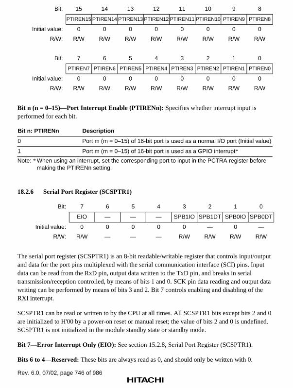
Rev. 6.0, 07/02, page 746 of 986
Bit: 15 14 13 12 11 10 9 8
PTIREN15 PTIREN14 PTIREN13 PTIREN12 PTIREN11 PTIREN10 PTIREN9 PTIREN8
Initial value: 0 0 0 0 0 0 0 0
R/W: R/W R/W R/W R/W R/W R/W R/W R/W
Bit: 7 6 5 4 3 2 1 0
PTIREN7 PTIREN6 PTIREN5 PTIREN4 PTIREN3 PTIREN2 PTIREN1 PTIREN0
Initial value: 0 0 0 0 0 0 0 0
R/W: R/W R/W R/W R/W R/W R/W R/W R/W
Bit n (n = 0–15)—Port Interrupt Enable (PTIRENn): Specifies whether interrupt input isperformed for each bit.
Bit n: PTIRENn Description
0 Port m (m = 0–15) of 16-bit port is used as a normal I/O port (Initial value)
1 Port m (m = 0–15) of 16-bit port is used as a GPIO interrupt*
Note: * When using an interrupt, set the corresponding port to input in the PCTRA register beforemaking the PTIRENn setting.
18.2.6 Serial Port Register (SCSPTR1)
Bit: 7 6 5 4 3 2 1 0
EIO — — — SPB1IO SPB1DT SPB0IO SPB0DT
Initial value: 0 0 0 0 0 — 0 —
R/W: R/W — — — R/W R/W R/W R/W
The serial port register (SCSPTR1) is an 8-bit readable/writable register that controls input/outputand data for the port pins multiplexed with the serial communication interface (SCI) pins. Inputdata can be read from the RxD pin, output data written to the TxD pin, and breaks in serialtransmission/reception controlled, by means of bits 1 and 0. SCK pin data reading and output datawriting can be performed by means of bits 3 and 2. Bit 7 controls enabling and disabling of theRXI interrupt.
SCSPTR1 can be read or written to by the CPU at all times. All SCSPTR1 bits except bits 2 and 0are initialized to H'00 by a power-on reset or manual reset; the value of bits 2 and 0 is undefined.SCSPTR1 is not initialized in the module standby state or standby mode.
Bit 7—Error Interrupt Only (EIO): See section 15.2.8, Serial Port Register (SCSPTR1).
Bits 6 to 4—Reserved: These bits are always read as 0, and should only be written with 0.

Rev. 6.0, 07/02, page 747 of 986
Bit 3—Serial Port Clock Port I/O (SPB1IO): Specifies serial port SCK pin input/output. Whenthe SCK pin is actually set as a port output pin and outputs the value set by the SPB1DT bit, theC/A bit in SCSMR1 and the CKE1 and CKE0 bits in SCSCR1 should be cleared to 0.
Bit 3: SPB1IO Description
0 SPB1DT bit value is not output to the SCK pin (Initial value)
1 SPB1DT bit value is output to the SCK pin
Bit 2—Serial Port Clock Port Data (SPB1DT): Specifies the serial port SCK pin input/outputdata. Input or output is specified by the SPB1IO bit (see the description of bit 3, SPB1IO, fordetails). When output is specified, the value of the SPB1DT bit is output to the SCK pin. The SCKpin value is read from the SPB1DT bit regardless of the value of the SPB1IO bit. The initial valueof this bit after a power-on reset or manual reset is undefined.
Bit 2: SPB1DT Description
0 Input/output data is low-level
1 Input/output data is high-level
Bit 1—Serial Port Break I/O (SPB0IO): Specifies the serial port TxD pin output condition.When the TxD pin is actually set as a port output pin and outputs the value set by the SPB0DT bit,the TE bit in SCSCR1 should be cleared to 0.
Bit 1: SPB0IO Description
0 SPB0DT bit value is not output to the TxD pin (Initial value)
1 SPB0DT bit value is output to the TxD pin
Bit 0—Serial Port Break Data (SPB0DT): Specifies the serial port RxD pin input data and TxDpin output data. The TxD pin output condition is specified by the SPB0IO bit (see the descriptionof bit 1, SPB0IO, for details). When the TxD pin is designated as an output, the value of theSPB0DT bit is output to the TxD pin. The RxD pin value is read from the SPB0DT bit regardlessof the value of the SPB0IO bit. The initial value of this bit after a power-on reset or manual resetis undefined.
Bit 0: SPB0DT Description
0 Input/output data is low-level
1 Input/output data is high-level

Rev. 6.0, 07/02, page 748 of 986
18.2.7 Serial Port Register (SCSPTR2)
Bit: 15 14 13 12 11 10 9 8
— — — — — — — —
Initial value: 0 0 0 0 0 0 0 0
R/W: R R R R R R R R
Bit: 7 6 5 4 3 2 1 0
RTSIO RTSDT CTSIO CTSDT — — SPB2IO SPB2DT
Initial value: 0 — 0 — 0 0 0 —
R/W: R/W R/W R/W R/W R R R/W R/W
The serial port register (SCSPTR2) is a 16-bit readable/writable register that controls input/outputand data for the port pins multiplexed with the serial communication interface (SCIF) pins. Inputdata can be read from the RxD2 pin, output data written to the TxD2 pin, and breaks in serialtransmission/reception controlled, by means of bits 1 and 0. CTS2 pin data reading and output datawriting can be performed by means of bits 5 and 4, and RTS2 pin data reading and output datawriting by means of bits 7 and 6.
SCSPTR2 can be read or written to by the CPU at all times. All SCSPTR2 bits except bits 6, 4,and 0 are initialized to 0 by a power-on reset or manual reset; the value of bits 6, 4, and 0 isundefined. SCSPTR2 is not initialized in standby mode or in the module standby state.
Bits 15 to 8—Reserved: These bits are always read as 0, and should only be written with 0.
Bit 7—Serial Port RTS Port I/O (RTSIO): Specifies serial port RTS2 pin input/output. Whenthe RTS2 pin is actually set as a port output pin and outputs the value set by the RTSDT bit, theMCE bit in SCFCR2 should be cleared to 0.
Bit 7: RTSIO Description
0 RTSDT bit value is not output to the RTS2 pin (Initial value)
1 RTSDT bit value is output to the RTS2 pin

Rev. 6.0, 07/02, page 749 of 986
Bit 6—Serial Port RTS Port Data (RTSDT): Specifies the serial port RTS2 pin input/outputdata. Input or output is specified by the RTSIO pin (see the description of bit 7, RTSIO, fordetails). When the RTS2 pin is designated as an output, the value of the RTSDT bit is output to theRTS2 pin. The RTS2 pin value is read from the RTSDT bit regardless of the value of the RTSIObit. The initial value of this bit after a power-on reset or manual reset is undefined.
Bit 6: RTSDT Description
0 Input/output data is low-level
1 Input/output data is high-level
Bit 5—Serial Port CTS Port I/O (CTSIO): Specifies serial port CTS2 pin input/output. Whenthe CTS2 pin is actually set as a port output pin and outputs the value set by the CTSDT bit, theMCE bit in SCFCR2 should be cleared to 0.
Bit 5: CTSIO Description
0 CTSDT bit value is not output to the CTS2 pin (Initial value)
1 CTSDT bit value is output to the CTS2 pin
Bit 4—Serial Port CTS Port Data (CTSDT): Specifies the serial port CTS2 pin input/outputdata. Input or output is specified by the CTSIO pin (see the description of bit 5, CTSIO, fordetails). When the CTS2 pin is designated as an output, the value of the CTSDT bit is output to theCTS2 pin. The CTS2 pin value is read from the CTSDT bit regardless of the value of the CTSIObit. The initial value of this bit after a power-on reset or manual reset is undefined.
Bit 4: CTSDT Description
0 Input/output data is low-level
1 Input/output data is high-level
Bits 3 and 2—Reserved: These bits are always read as 0, and should only be written with 0.
Bit 1—Serial Port Break I/O (SPB2IO): Specifies the serial port TxD2 pin output condition.When the TxD2 pin is actually set as a port output pin and outputs the value set by the SPB2DTbit, the TE bit in SCSCR2 should be cleared to 0.
Bit 1: SPB2IO Description
0 SPB2DT bit value is not output to the TxD2 pin (Initial value)
1 SPB2DT bit value is output to the TxD2 pin

Rev. 6.0, 07/02, page 750 of 986
Bit 0—Serial Port Break Data (SPB2DT): Specifies the serial port RxD2 pin input data andTxD2 pin output data. The TxD2 pin output condition is specified by the SPB2IO bit (see thedescription of bit 1, SPB2IO, for details). When the TxD2 pin is designated as an output, the valueof the SPB2DT bit is output to the TxD2 pin. The RxD2 pin value is read from the SPB2DT bitregardless of the value of the SPB2IO bit. The initial value of this bit after a power-on reset ormanual reset is undefined.
Bit 0: SPB2DT Description
0 Input/output data is low-level
1 Input/output data is high-level

Rev. 6.0, 07/02, page 751 of 986
Section 19 Interrupt Controller (INTC)
19.1 Overview
The interrupt controller (INTC) ascertains the priority of interrupt sources and controls interruptrequests to the CPU. The INTC registers set the order of priority of each interrupt, allowing theuser to handle interrupt requests according to user-set priority.
19.1.1 Features
The INTC has the following features.
• Fifteen interrupt priority levels can be set
By setting the three interrupt priority registers, the priorities of on-chip peripheral moduleinterrupts can be selected from 15 levels for different request sources.
• NMI noise canceler function
The NMI input level bit indicates the NMI pin state. The pin state can be checked by readingthis bit in the interrupt exception service routine, enabling it to be used as a noise canceler.
• NMI request masking when SR.BL bit is set to 1
It is possible to select whether or not NMI requests are to be masked when the SR.BL bit is setto 1.
19.1.2 Block Diagram
Figure 19.1 shows a block diagram of the INTC.

Rev. 6.0, 07/02, page 752 of 986
TMU: Timer unitRTC: Realtime clock unitSCI: Serial communication interfaceSCIF: Serial communication interface with FIFOWDT: Watchdog timerREF: Memory refresh controller section of the bus state controllerDMAC: Direct memory access controllerH-UDI: Hitachi user debug interfaceGPIO: I/O portICR: Interrupt control registerIPRA–IPRD: Interrupt priority registers A–D*1
INTPRI00: Interrupt priority level setting register 00*2
SR: Status register
Notes: *1 IPRD is provided only in the SH7750S and SH7750R.*2 INTPRI00 is provided only in the SH7750R.
NMIInput control
–
TMU
RTC
SCI
SCIF
WDT
REF
DMAC
H-UDI
GPIO
Priorityidentifier
4 4
(Interrupt request)Com-parator
Bus interface
Inte
rnal
bus
ICRIPRA–IPRD*1
INTPRI00*2
(Interrupt request)
(Interrupt request)
(Interrupt request)
(Interrupt request)
(Interrupt request)
(Interrupt request)
(Interrupt request)
(Interrupt request)
INTC
Interruptrequest
I3 I2 I1 I0
SR
CPU
IPR
Figure 19.1 Block Diagram of INTC

Rev. 6.0, 07/02, page 753 of 986
19.1.3 Pin Configuration
Table 19.1 shows the INTC pin configuration.
Table 19.1 INTC Pins
Pin Name Abbreviation I/O Function
Nonmaskable interruptinput pin
NMI Input Input of nonmaskable interrupt requestsignal
Interrupt input pins IRL3–IRL0 Input Input of interrupt request signals(maskable by I3–I0 in SR)
19.1.4 Register Configuration
The INTC has the registers shown in table 19.2.
Table 19.2 INTC Registers
Name Abbreviation R/WInitial Value*1
P4 AddressArea 7Address
AccessSize
Interrupt controlregister
ICR R/W *2 H'FFD00000 H'1FD00000 16
Interrupt priorityregister A
IPRA R/W H'0000 H'FFD00004 H'1FD00004 16
Interrupt priorityregister B
IPRB R/W H'0000 H'FFD00008 H'1FD00008 16
Interrupt priorityregister C
IPRC R/W H'0000 H'FFD0000C H'1FD0000C 16
Interrupt priorityregister D*3
IPRD R/W H'DA74 H'FFD00010 H'1FD00010 16
Interrupt prioritylevel settingregister 00*4
INTPRI00 R/W H'00000000 H'FE080000 H'1E080000 32
Interrupt sourceregister 00*4
INTREQ00 R H'00000000 H'FE080020 H'1E080020 32
Interrupt maskregister 00*4
INTMSK00 R/W H'00000300 H'FE080040 H'1E080040 32
Interrupt maskclear register 00*4
INTMSKCLR00 R — H'FE080060 H'1E080060 32
Notes: *1 Initialized by a power-on reset or manual reset.
*2 H'8000 when the NMI pin is high, H'0000 when the NMI pin is low.*3 SH7750S and SH7750R only*4 SH7750R only

Rev. 6.0, 07/02, page 754 of 986
19.2 Interrupt Sources
There are three types of interrupt sources: NMI, RL, and on-chip peripheral modules. Eachinterrupt has a priority level (16–0), with level 16 as the highest and level 1 as the lowest. Whenlevel 0 is set, the interrupt is masked and interrupt requests are ignored.
19.2.1 NMI Interrupt
The NMI interrupt has the highest priority level of 16. It is always accepted unless the BL bit inthe status register in the CPU is set to 1. In sleep or standby mode, the interrupt is accepted even ifthe BL bit is set to 1.
A setting can also be made to have the NMI interrupt accepted even if the BL bit is set to 1.
Input from the NMI pin is edge-detected. The NMI edge select bit (NMIE) in the interrupt controlregister (ICR) is used to select either rising or falling edge. When the NMIE bit in the ICR registeris modified, the NMI interrupt is not detected for a maximum of 6 bus clock cycles after themodification.
NMI interrupt exception handling does not affect the interrupt mask level bits (I3–I0) in the statusregister (SR).

Rev. 6.0, 07/02, page 755 of 986
19.2.2 IRL Interrupts
IRL interrupts are input by level at pins IRL3–IRL0. The priority level is the level indicated bypins IRL3–IRL0. An IRL3–IRL0 value of 0 (0000) indicates the highest-level interrupt request(interrupt priority level 15). A value of 15 (1111) indicates no interrupt request (interrupt prioritylevel 0).
Interrupt requests
Priorityencoder
to
4
SH7750 Series
to
Figure 19.2 Example of IRL Interrupt Connection

Rev. 6.0, 07/02, page 756 of 986
Table 19.3 IRL3IRL3IRL3IRL3–IRL0IRL0IRL0IRL0 Pins and Interrupt Levels
IRL3IRL3IRL3IRL3 IRL2IRL2IRL2IRL2 IRL1IRL1IRL1IRL1 IRL0IRL0IRL0IRL0 Interrupt Priority Level Interrupt Request
0 0 0 0 15 Level 15 interrupt request
1 14 Level 14 interrupt request
1 0 13 Level 13 interrupt request
1 12 Level 12 interrupt request
1 0 0 11 Level 11 interrupt request
1 10 Level 10 interrupt request
1 0 9 Level 9 interrupt request
1 8 Level 8 interrupt request
1 0 0 0 7 Level 7 interrupt request
1 6 Level 6 interrupt request
1 0 5 Level 5 interrupt request
1 4 Level 4 interrupt request
1 0 0 3 Level 3 interrupt request
1 2 Level 2 interrupt request
1 0 1 Level 1 interrupt request
1 0 No interrupt request
A noise-cancellation feature is built in, and the IRL interrupt is not detected unless the levelssampled at every bus clock cycle remain unchanged for three consecutive cycles, so that notransient level on the IRL pin change is detected. In standby mode, as the bus clock is stopped,noise cancellation is performed using the 32.768 kHz clock for the RTC instead. When the RTC isnot used, therefore, interruption by means of IRL interrupts cannot be performed in standby mode.
The priority level of the IRL interrupt must not be lowered unless the interrupt is accepted and theinterrupt handling starts. However, the priority level can be changed to a higher one.
The interrupt mask bits (I3–I0) in the status register (SR) are not affected by IRL interrupthandling.
Pins IRL0–IRL3 can be used for four independent interrupt requests by setting the IRLM bit to 1in the ICR register. When independent interrupt requests are used in the SH7750, the interruptpriority levels are fixed (table 19.4). When independent interrupt requests are used in theSH7750S or SH7750R, the interrupt priority levels can be set in interrupt priority register D(IPRD).

Rev. 6.0, 07/02, page 757 of 986
Table 19.4 SH7750 IRL3IRL3IRL3IRL3–IRL0IRL0IRL0IRL0 Pins and Interrupt Levels (When IRLM = 1)
IRL3IRL3IRL3IRL3 IRL2IRL2IRL2IRL2 IRL1IRL1IRL1IRL1 IRL0IRL0IRL0IRL0 Interrupt Priority Level Interrupt Request
1/0 1/0 1/0 0 13 IRL0
1/0 1/0 0 1 10 IRL1
1/0 0 1 1 7 IRL2
0 1 1 1 4 IRL3
19.2.3 On-Chip Peripheral Module Interrupts
On-chip peripheral module interrupts are generated by the following nine modules:
• Hitachi user debug interface (H-UDI)
• Direct memory access controller (DMAC)
• Timer unit (TMU)
• Realtime clock (RTC)
• Serial communication interface (SCI)
• Serial communication interface with FIFO (SCIF)
• Bus state controller (BSC)
• Watchdog timer (WDT)
• I/O port (GPIO)
Not every interrupt source is assigned a different interrupt vector, bus sources are reflected in theinterrupt event register (INTEVT), so it is easy to identify sources by using the INTEVT registervalue as a branch offset in the exception handling routine.
A priority level from 15 to 0 can be set for each module by means of interrupt priority registers Ato D (IPRA–IPRD), 00 (INTPRI00).
The interrupt mask bits (I3–I0) in the status register (SR) are not affected by on-chip peripheralmodule interrupt handling.
On-chip peripheral module interrupt source flag and interrupt enable flag updating should only becarried out when the BL bit in the status register (SR) is set to 1. To prevent acceptance of anerroneous interrupt from an interrupt source that should have been updated, first read the on-chipperipheral register containing the relevant flag, then clear the BL bit to 0. In the case of interruptson channel 3 or 4 of the TMU, also read from the interrupt source register 00 (INTREQ00). Thiswill secure the necessary timing internally. When updating a number of flags, there is no problemif only the register containing the last flag updated is read.

Rev. 6.0, 07/02, page 758 of 986
If flag updating is performed while the BL bit is cleared to 0, the program may jump to theinterrupt handling routine when the INTEVT register value is 0. In this case, interrupt handling isinitiated due to the timing relationship between the flag update and interrupt request recognitionwithin the chip. Processing can be continued without any problem by executing an RTEinstruction.
19.2.4 Interrupt Exception Handling and Priority
Table 19.5 lists the codes for the interrupt event register (INTEVT), and the order of interruptpriority. Each interrupt source is assigned a unique INTEVT code. The start address of theinterrupt handler is common to each interrupt source. This is why, for instance, the value ofINTEVT is used as an offset at the start of the interrupt handler and branched to in order toidentify the interrupt source.
The order of priority of the on-chip peripheral modules is specified as desired by setting prioritylevels from 0 to 15 in interrupt priority registers A to D (IPRA–IPRD). The order of priority of theon-chip peripheral modules is set to 0 by a reset.
When the priorities for multiple interrupt sources are set to the same level and such interrupts aregenerated simultaneously, they are handled according to the default priority order shown in table19.5.
Updating of interrupt priority registers A to D, 00 should only be carried out when the BL bit inthe status register (SR) is set to 1. To prevent erroneous interrupt acceptance, first read one of theinterrupt priority registers, then clear the BL bit to 0. This will secure the necessary timinginternally.
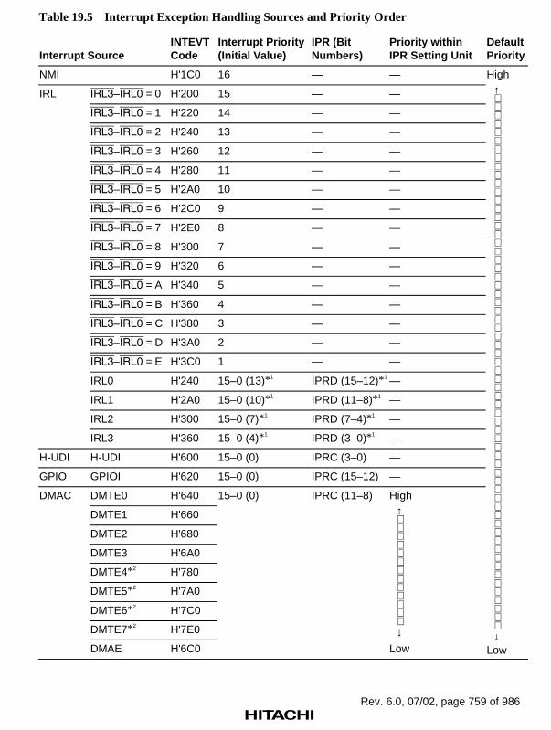
Rev. 6.0, 07/02, page 759 of 986
Table 19.5 Interrupt Exception Handling Sources and Priority Order
Interrupt SourceINTEVTCode
Interrupt Priority(Initial Value)
IPR (BitNumbers)
Priority withinIPR Setting Unit
DefaultPriority
NMI H'1C0 16 — — High
IRL IRL3–IRL0 = 0 H'200 15 — —
IRL3–IRL0 = 1 H'220 14 — —
IRL3–IRL0 = 2 H'240 13 — —
IRL3–IRL0 = 3 H'260 12 — —
IRL3–IRL0 = 4 H'280 11 — —
IRL3–IRL0 = 5 H'2A0 10 — —
IRL3–IRL0 = 6 H'2C0 9 — —
IRL3–IRL0 = 7 H'2E0 8 — —
IRL3–IRL0 = 8 H'300 7 — —
IRL3–IRL0 = 9 H'320 6 — —
IRL3–IRL0 = A H'340 5 — —
IRL3–IRL0 = B H'360 4 — —
IRL3–IRL0 = C H'380 3 — —
IRL3–IRL0 = D H'3A0 2 — —
IRL3–IRL0 = E H'3C0 1 — —
IRL0 H'240 15–0 (13)*1 IPRD (15–12)*1 —
IRL1 H'2A0 15–0 (10)*1 IPRD (11–8)*1 —
IRL2 H'300 15–0 (7)*1 IPRD (7–4)*1 —
IRL3 H'360 15–0 (4)*1 IPRD (3–0)*1 —
H-UDI H-UDI H'600 15–0 (0) IPRC (3–0) —
GPIO GPIOI H'620 15–0 (0) IPRC (15–12) —
DMAC DMTE0 H'640 15–0 (0) IPRC (11–8) High
DMTE1 H'660
DMTE2 H'680
DMTE3 H'6A0
DMTE4*2 H'780
DMTE5*2 H'7A0
DMTE6*2 H'7C0
DMTE7*2 H'7E0
↑↓
DMAE H'6C0 Low
↑↓
Low
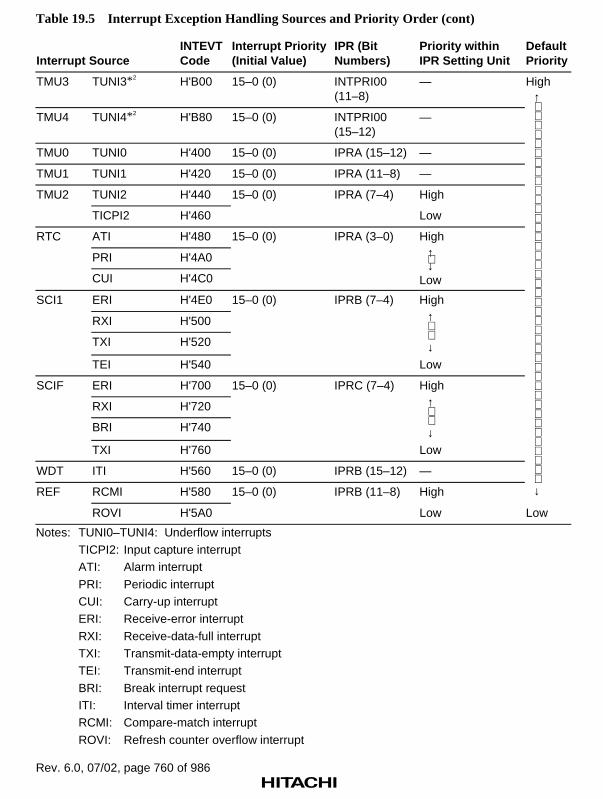
Rev. 6.0, 07/02, page 760 of 986
Table 19.5 Interrupt Exception Handling Sources and Priority Order (cont)
Interrupt SourceINTEVTCode
Interrupt Priority(Initial Value)
IPR (BitNumbers)
Priority withinIPR Setting Unit
DefaultPriority
TMU3 TUNI3*2 H'B00 15–0 (0) INTPRI00(11–8)
—
TMU4 TUNI4*2 H'B80 15–0 (0) INTPRI00(15–12)
—
TMU0 TUNI0 H'400 15–0 (0) IPRA (15–12) —
TMU1 TUNI1 H'420 15–0 (0) IPRA (11–8) —
TMU2 TUNI2 H'440 15–0 (0) IPRA (7–4) High
TICPI2 H'460 Low
RTC ATI H'480 15–0 (0) IPRA (3–0)
PRI H'4A0
CUI H'4C0
High↑↓
Low
SCI1 ERI H'4E0 15–0 (0) IPRB (7–4) High
RXI H'500
TXI H'520
↑↓
TEI H'540 Low
SCIF ERI H'700 15–0 (0) IPRC (7–4) High
RXI H'720
BRI H'740
↑↓
TXI H'760 Low
WDT ITI H'560 15–0 (0) IPRB (15–12) —
REF RCMI H'580 15–0 (0) IPRB (11–8) High
High↑↓
ROVI H'5A0 Low Low
Notes: TUNI0–TUNI4: Underflow interruptsTICPI2: Input capture interruptATI: Alarm interrupt
PRI: Periodic interruptCUI: Carry-up interruptERI: Receive-error interrupt
RXI: Receive-data-full interruptTXI: Transmit-data-empty interruptTEI: Transmit-end interrupt
BRI: Break interrupt requestITI: Interval timer interruptRCMI: Compare-match interrupt
ROVI: Refresh counter overflow interrupt

Rev. 6.0, 07/02, page 761 of 986
H-UDI: Hitachi use debug interface
GPIOI: I/O port interruptDMTE0–DMTE7: DMAC transfer end interruptsDMAE: DMAC address error interrupt*1 Interrupt priority levels can only be changed in the SH7750S or SH7750R. In the
SH7750, the initial values cannot be changed.
*2 SH7750R only
19.3 Register Descriptions
19.3.1 Interrupt Priority Registers A to D (IPRA–IPRD)
Interrupt priority registers A to D (IPRA–IPRD) are 16-bit readable/writable registers that setpriority levels from 0 to 15 for on-chip peripheral module interrupts. IPRA to IPRC are initializedto H'0000 and IPRD is to H'DA74 by a reset. They are not initialized in standby mode.
IPRA to IPRC
Bit: 15 14 13 12 11 10 9 8
Initial value: 0 0 0 0 0 0 0 0
R/W: R/W R/W R/W R/W R/W R/W R/W R/W
Bit: 7 6 5 4 3 2 1 0
Initial value: 0 0 0 0 0 0 0 0
R/W: R/W R/W R/W R/W R/W R/W R/W R/W
IPRD (SH7750S and SH7750R only)
Bit: 15 14 13 12 11 10 9 8
Initial value: 1 1 0 1 1 0 1 0
R/W: R/W R/W R/W R/W R/W R/W R/W R/W
Bit: 7 6 5 4 3 2 1 0
Initial value: 0 1 1 1 0 1 0 0
R/W: R/W R/W R/W R/W R/W R/W R/W R/W

Rev. 6.0, 07/02, page 762 of 986
Table 19.6 shows the relationship between the interrupt request sources and the IPRA–IPRDregister bits.
Table 19.6 Interrupt Request Sources and IPRA–IPRD Registers
Bits
Register 15–12 11–8 7–4 3–0
Interrupt priority register A TMU0 TMU1 TMU2 RTC
Interrupt priority register B WDT REF*1 SCI1 Reserved*2
Interrupt priority register C GPIO DMAC SCIF H-UDI
Interrupt priority register D*3 IRL0 IRL1 IRL2 IRL3
Notes: *1 REF is the memory refresh unit in the bus state controller (BSC). See section 13, BusState Controller (BSC), for details.
*2 Reserved bits: These bits are always read as 0 and should always be written with 0.
*3 SH7750S and SH7750R only
As shown in table 19.6, four on-chip peripheral modules are assigned to each register. Interruptpriority levels are established by setting a value from H'F (1111) to H'0 (0000) in each of the four-bit groups: 15–12, 11–8, 7–4, and 3–0. Setting H'F designates priority level 15 (the highest level),and setting H'0 designates priority level 0 (requests are masked).
19.3.2 Interrupt Control Register (ICR)
The interrupt control register (ICR) is a 16-bit register that sets the input signal detection mode forexternal interrupt input pin NMI and indicates the input signal level at the NMI pin. This registeris initialized by a power-on reset or manual reset. It is not initialized in standby mode.
Bit: 15 14 13 12 11 10 9 8
Bit name: NMIL MAI — — — — NMIB NMIE
Initial value: 0/1* 0 0 0 0 0 0 0
R/W: R R/W — — — — R/W R/W
Bit: 7 6 5 4 3 2 1 0
Bit name: IRLM — — — — — — —
Initial value: 0 0 0 0 0 0 0 0
R/W: R/W — — — — — — —
Note: * 1 when NMI pin input is high, 0 when low.

Rev. 6.0, 07/02, page 763 of 986
Bit 15—NMI Input Level (NMIL): Sets the level of the signal input at the NMI pin. This bit canbe read to determine the NMI pin level. It cannot be modified.
Bit 15: NMIL Description
0 NMI pin input level is low
1 NMI pin input level is high
Bit 14—NMI Interrupt Mask (MAI): Specifies whether or not all interrupts are to be maskedwhile the NMI pin input level is low, irrespective of the CPU’s SR.BL bit.
Bit 14: MAI Description
0 Interrupts enabled even while NMI pin is low (Initial value)
1 Interrupts disabled while NMI pin is low*
Note: * NMI interrupts are accepted in normal operation and in sleep mode.In standby mode, all interrupts are masked, and standby is not cleared, while the NMI pin islow.
Bit 9—NMI Block Mode (NMIB): Specifies whether an NMI request is to be held pending ordetected immediately while the SR.BL bit is set to 1.
Bit 9: NMIB Description
0 NMI interrupt requests held pending while SR.BL bit is set to 1(Initial value)
1 NMI interrupt requests detected while SR.BL bit is set to 1
Notes: 1. If interrupt requests are enabled while SR.BL = 1, the previous exception informationwill be lost, and so must be saved beforehand.
2. This bit is cleared automatically by NMI acceptance.
Bit 8—NMI Edge Select (NMIE): Specifies whether the falling or rising edge of the interruptrequest signal to the NMI pin is detected.
Bit 8: NMIE Description
0 Interrupt request detected on falling edge of NMI input (Initial value)
1 Interrupt request detected on rising edge of NMI input
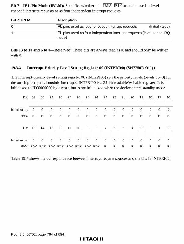
Rev. 6.0, 07/02, page 764 of 986
Bit 7—IRL Pin Mode (IRLM): Specifies whether pins IRL3–IRL0 are to be used as level-encoded interrupt requests or as four independent interrupt requests.
Bit 7: IRLM Description
0 IRL pins used as level-encoded interrupt requests (Initial value)
1 IRL pins used as four independent interrupt requests (level-sense IRQmode)
Bits 13 to 10 and 6 to 0—Reserved: These bits are always read as 0, and should only be writtenwith 0.
19.3.3 Interrupt-Priority-Level Setting Register 00 (INTPRI00) (SH7750R Only)
The interrupt-priority-level setting register 00 (INTPRI00) sets the priority levels (levels 15–0) forthe on-chip peripheral module interrupts. INTPRI00 is a 32-bit readable/writable register. It isinitialized to H'00000000 by a reset, but is not initialized when the device enters standby mode.
Bit: 31 30 29 28 27 26 25 24 23 22 21 20 19 18 17 16
Initial value: 0 0 0 0 0 0 0 0 0 0 0 0 0 0 0 0
R/W: R R R R R R R R R R R R R R R R
Bit: 15 14 13 12 11 10 9 8 7 6 5 4 3 2 1 0
Initial value: 0 0 0 0 0 0 0 0 0 0 0 0 0 0 0 0
R/W: R/W R/W R/W R/W R/W R/W R/W R/W R R R R R R R R
Table 19.7 shows the correspondence between interrupt request sources and the bits in INTPRI00.

Rev. 6.0, 07/02, page 765 of 986
Table 19.7 Interrupt Request Sources and the Bits of the INTPRI00 Register
Bit
Register 31 to 28 27 to 24 23 to 20 19 to 16 15 to 12 11 to 8 7 to 4 3 to 0
Interrupt-priority-levelsettingregister 00
Reserved Reserved Reserved Reserved TMU ch4 TMU ch3 Reserved Reserved
Note: As shown in the table above, levels for all eight on-chip peripheral modules are assigned ina single register. The interrupt priority level for the interrupt source that corresponds to eachset of four bits is set as a value from H'F (1111) to H'0 (0000). The setting H'F selectsinterrupt priority level 15, which is the highest, and H'0 selects level 0, which means thatinterrupt requests from that source are masked.Reserved bits are always read as 0. When writing, only 0s should be written to these bits.
19.3.4 Interrupt Source Register 00 (INTREQ00) (SH7750R Only)
The interrupt source register 00 (INTREQ00) indicates the origin of the interrupt request that hasbeen sent to the INTC. The states of the bits in this register is not affected by masking of thecorresponding interrupts by the settings in the INTPRI00 or INTMSK00 register. INTREQ00 is a32-bit read-only register.
Bit: 31 30 29 28 27 26 25 24 23 22 21 20 19 18 17 16
Initial value: 0 0 0 0 0 0 0 0 0 0 0 0 0 0 0 0
R/W: R R R R R R R R R R R R R R R R
Bit: 15 14 13 12 11 10 9 8 7 6 5 4 3 2 1 0
Initial value: 0 0 0 0 0 0 0 0 0 0 0 0 0 0 0 0
R/W: R R R R R R R R R R R R R R R R
Bit 31 to 0—Interrupt Request: Each of the non-reserved bits in this register indicates that thereis an interrupt request relevant to that bit. For the correspondence between the bits and interruptsources, see section 19.3.7, Bit Assignments of INTREQ00, INTMSK00, and INTMSKCLR00(SH7750R Only).
Bits 31 to 0 Description
0 There is no interrupt request that corresponds to this bit
1 There is an interrupt request that corresponds to this bit.

Rev. 6.0, 07/02, page 766 of 986
19.3.5 Interrupt Mask Register 00 (INTMSK00) (SH7750R Only)
The interrupt mask register 00 (INTMSK00) sets the masking of individual interrupt requests.INTMSK00 is a 32-bit register. It is initialized to H'000003FF by a reset, and retains this value instandby mode.
To cancel masking of an interrupt, write a 1 to the corresponding bit in the INTMSKCLR00register. Note that writing a 0 to a bit in INTMSK00 does not change its value.
Bit: 31 30 29 28 27 26 25 24 23 22 21 20 19 18 17 16
Initial value: 0 0 0 0 0 0 0 0 0 0 0 0 0 0 0 0
R/W: R R R R R R R R R R R R R R R R
Bit: 15 14 13 12 11 10 9 8 7 6 5 4 3 2 1 0
Initial value: 0 0 0 0 0 1 1 1 1 1 1 1 1 1 1 1
R/W: R R R R R R/W R/W R/W R/W R/W R/W R/W R/W R/W R/W R/W
Bit 31 to 0—Interrupt Mask: Sets the masking of the interrupt request that corresponds to thegiven bit. For the correspondence between bits and interrupt sources, see section 19.3.7, BitAssignments of INTREQ00, INTMSK00, and INTMSKCLR00 (SH7750R Only).
Bits 31 to 0 Description
0 Interrupt requests from the source that corresponds to this bit areaccepted
1 Interrupt requests from the source that corresponds to this bit aremasked (Initial value)

Rev. 6.0, 07/02, page 767 of 986
19.3.6 Interrupt Mask Clear Register 00 (INTMSKCLR00) (SH7750R Only)
The interrupt mask clear register 00 (INTMSKCLR00) clears the masking of individual interruptrequests. INTMSKCLR00 is a 32-bit write-only register.
Bit: 31 30 29 28 27 26 25 24 23 22 21 20 19 18 17 16
Initial value: — — — — — — — — — — — — — — — —
R/W: W W W W W W W W W W W W W W W W
Bit: 15 14 13 12 11 10 9 8 7 6 5 4 3 2 1 0
Initial value: — — — — — — — — — — — — — — — —
R/W: W W W W W W W W W W W W W W W W
Bit 31 to 0 Interrupt Mask Clear: Each bit selects whether or not to clear the masking of theinterrupt source that corresponds to that bit. For the correspondence between the bits and interruptsources, see section 19.3.7, Bit Assignments of INTREQ00, INTMSK00, and INTMSKCLR00(SH7750R Only).
Bits 31 to 0 Description
0 Masking of interrupt requests from the source that corresponds to thebit is not changed
1 Masking of interrupt requests from the source that corresponds to thebit is cleared
19.3.7 Bit Assignments of INTREQ00, INTMSK00, and INTMSKCLR00
(SH7750R Only)
The relationship between the bits in these registers and interrupt sources is as shown below.
Table 19.8 Bit Assignments
Bit number Module Interrupt
31 to 10, 7 to 0 Reserved Reserved
9 TMU TUNI4
8 TMU TUNI3

Rev. 6.0, 07/02, page 768 of 986
19.4 INTC Operation
19.4.1 Interrupt Operation Sequence
The sequence of operations when an interrupt is generated is described below. Figure 19.3 shows aflowchart of the operations.
1. The interrupt request sources send interrupt request signals to the interrupt controller.
2. The interrupt controller selects the highest-priority interrupt from the interrupt requests sent,according to the priority levels set in interrupt priority registers A to C (IPRA–IPRC). Lower-priority interrupts are held pending. If two of these interrupts have the same priority level, or ifmultiple interrupts occur within a single module, the interrupt with the highest priorityaccording to table 19.5, Interrupt Exception Handling Sources and Priority Order, is selected.
3. The priority level of the interrupt selected by the interrupt controller is compared with theinterrupt mask bits (I3–I0) in the status register (SR) of the CPU. If the request priority level ishigher that the level in bits I3–I0, the interrupt controller accepts the interrupt and sends aninterrupt request signal to the CPU.
4. The CPU accepts an interrupt at a break between instructions.
5. The interrupt source code is set in the interrupt event register (INTEVT).
6. The status register (SR) and program counter (PC) are saved to SSR and SPC, respectively.The R15 contents at this time are saved in SGR.
7. The block bit (BL), mode bit (MD), and register bank bit (RB) in SR are set to 1.
8. The CPU jumps to the start address of the interrupt handler (the sum of the value set in thevector base register (VBR) and H'00000600).
The interrupt handler may branch with the INTEVT register value as its offset in order to identifythe interrupt source. This enables it to branch to the handling routine for the particular interruptsource.
Notes: 1. The interrupt mask bits (I3–I0) in the status register (SR) are not changed byacceptance of an interrupt in the SH7750 Series.
2. The interrupt source flag should be cleared in the interrupt handler. To ensure that aninterrupt request that should have been cleared is not inadvertently accepted again, readthe interrupt source flag after it has been cleared, then wait for the interval shown intable 19.7 (Time for priority decision and SR mask bit comparison) before clearing theBL bit or executing an RTE instruction.
3. For some interrupt sources, their interrupt masks (INTMSK00) must e cleared usingthe INTMSKCLR00 register.

Rev. 6.0, 07/02, page 769 of 986
Programexecution state
No
No
Yes
No
Yes
No
Yes
Yes
No
No
Yes
Yes
No
Yes
No
No
YesNo
Yes
Save SR to SSR;save PC to SPC
Set interrupt sourcein INTEVT
Set BL, MD, RB bitsin SR to 1
Branch to exceptionhandler
Interruptgenerated?
(BL bitin SR = 0) or
(sleep or standbymode)?
NMI?
Level 14interrupt?
Level 1interrupt?I3–I0 =
level 13 orlower?
I3–I0 =level 0?
Yes
Level 15interrupt?
I3–I0* =level 14 or
lower?
Note: * I3–I0: Interrupt mask bits in status register (SR)
NMIB inICR = 1 and
NMI?
Figure 19.3 Interrupt Operation Flowchart

Rev. 6.0, 07/02, page 770 of 986
19.4.2 Multiple Interrupts
When handling multiple interrupts, interrupt handling should include the following procedures:
1. Branch to a specific interrupt handler corresponding to a code set in the INTEVT register. Thecode in INTEVT can be used as a branch-offset for branching to the specific handler.
2. Clear the interrupt source in the corresponding interrupt handler.
3. Save SPC and SSR to the stack.
4. Clear the BL bit in SR, and set the accepted interrupt level in the interrupt mask bits in SR.
5. Handle the interrupt.
6. Set the BL bit in SR to 1.
7. Restore SSR and SPC from memory.
8. Execute the RTE instruction.
When these procedures are followed in order, an interrupt of higher priority than the one beinghandled can be accepted after clearing BL in step 4. This enables the interrupt response time to beshortened for urgent processing.
19.4.3 Interrupt Masking with MAI Bit
By setting the MAI bit to 1 in the ICR register, it is possible to mask interrupts while the NMI pinis low, irrespective of the BL and IMASK bits in the SR register.
• In normal operation and sleep mode
All interrupts are masked while the NMI pin is low. However, an NMI interrupt only isgenerated by a transition at the NMI pin.
• In standby mode
All interrupts are masked while the NMI pin is low, and an NMI interrupt is not generated by atransition at the NMI pin. Therefore, standby cannot be cleared by an NMI interrupt while theMAI bit is set to 1.

Rev. 6.0, 07/02, page 771 of 986
19.5 Interrupt Response Time
The time from generation of an interrupt request until interrupt exception handling is performedand fetching of the first instruction of the exception service routine is started (the interruptresponse time) is shown in table 19.9.
Table 19.9 Interrupt Response Time
Number of States
Item NMI RLPeripheralModules Notes
Time for priority decision andSR mask bit comparison*
1Icyc + 4Bcyc 1Icyc + 7Bcyc 1Icyc + 2Bcyc
Wait time until end ofsequence being executed byCPU
S – 1 (≥ 0) ×Icyc
S – 1 (≥ 0) ×Icyc
S – 1 (≥ 0) ×Icyc
Time from interrupt exceptionhandling (save of SR and PC)until fetch of first instruction ofexception handler is started
4 × Icyc 4 × Icyc 4 × Icyc
Total 5Icyc + 4Bcyc+ (S – 1)Icyc
5Icyc + 7Bcyc+ (S – 1)Icyc
5Icyc + 2Bcyc+ (S – 1)Icyc
Minimumcase
13Icyc 19Icyc 9Icyc When Icyc:Bcyc = 2:1
Responsetime
Maximumcase
36 + S Icyc 60 + S Icyc 20 + S Icyc When Icyc:Bcyc = 8:1
Icyc: One cycle of internal clock supplied to CPU, etc.Bcyc: One CKIO cycleS: Latency of instructionNote: * In the SH7750 and SH7750S including the case where the mask bit (IMASK) in SR is
changed, and a new interrupt is generated.

Rev. 6.0, 07/02, page 772 of 986

Rev. 6.0, 07/02, page 773 of 986
Section 20 User Break Controller (UBC)
20.1 Overview
The user break controller (UBC) provides functions that simplify program debugging. When breakconditions are set in the UBC, a user break interrupt is generated according to the contents of thebus cycle generated by the CPU. This function makes it easy to design an effective self-monitoring debugger, enabling programs to be debugged with the chip alone, without using an in-circuit emulator.
20.1.1 Features
The UBC has the following features.
• Two break channels (A and B)
User break interrupts can be generated on independent conditions for channels A and B, or onsequential conditions (sequential break setting: channel A → channel B).
• The following can be set as break compare conditions:
Address (selection of 32-bit virtual address and ASID for comparison):
Address: All bits compared/lower 10 bits masked/lower 12 bits masked/lower 16 bitsmasked/lower 20 bits masked/all bits masked
ASID: All bits compared/all bits masked
Data (channel B only, 32-bit mask capability)
Bus cycle: Instruction access/operand access
Read/write
Operand size: Byte/word/longword/quadword
• An instruction access cycle break can be effected before or after the instruction is executed.

Rev. 6.0, 07/02, page 774 of 986
20.1.2 Block Diagram
Figure 20.1 shows a block diagram of the UBC.
Access control
Addressbus
Databus
Channel A
Accesscomparator
Addresscomparator
Channel B
Accesscomparator
Addresscomparator
Datacomparator
BBRA
BARA
BASRA
BAMRA
BBRB
BARB
BASRB
BAMRB
BDRB
BDMRB
BRCRControl
User break trap request
BBRA: Break bus cycle register ABARA: Break address register ABASRA: Break ASID register ABAMRA: Break address mask register ABBRB: Break bus cycle register BBARB: Break address register BBASRB: Break ASID register BBAMRB: Break address mask register BBDRB: Break data register BBDMRB: Break data mask register BBRCR: Break control register
Figure 20.1 Block Diagram of User Break Controller

Rev. 6.0, 07/02, page 775 of 986
Table 20.1 shows the UBC registers.
Table 20.1 UBC Registers
Name Abbreviation R/W Initial Value P4 AddressArea 7Address
AccessSize
Break addressregister A
BARA R/W Undefined H'FF200000 H'1F200000 32
Break addressmaskregister A
BAMRA R/W Undefined H'FF200004 H'1F200004 8
Break buscycle register A
BBRA R/W H'0000 H'FF200008 H'1F200008 16
Break ASIDregister A
BASRA R/W Undefined H'FF000014 H'1F000014 8
Break addressregister B
BARB R/W Undefined H'FF20000C H'1F20000C 32
Break addressmaskregister B
BAMRB R/W Undefined H'FF200010 H'1F200010 8
Break buscycle register B
BBRB R/W H'0000 H'FF200014 H'1F200014 16
Break ASIDregister B
BASRB R/W Undefined H'FF000018 H'1F000018 8
Break dataregister B
BDRB R/W Undefined H'FF200018 H'1F200018 32
Break datamask register B
BDMRB R/W Undefined H'FF20001C H'1F20001C 32
Break controlregister
BRCR R/W H'0000* H'FF200020 H'1F200020 16
Note: * Some bits are not initialized. See section 20.2.12, Break Control Register (BRCR), fordetails.

Rev. 6.0, 07/02, page 776 of 986
20.2 Register Descriptions
20.2.1 Access to UBC Control Registers
The access size must be the same as the control register size. If the sizes are different, a write willnot be effected in a UBC register write operation, and a read operation will return an undefinedvalue. UBC control register contents cannot be transferred to a floating-point register using afloating-point memory load instruction.
When a UBC control register is updated, use either of the following methods to make the updatedvalue valid:
1. Execute an RTE instruction after the memory store instruction that updated the register. Theupdated value will be valid from the RTE instruction jump destination onward.
2. Execute instructions requiring 5 states for execution after the memory store instruction thatupdated the register. As the SH7750 Series executes two instructions in parallel and aminimum of 0.5 state is required for execution of one instruction, 11 instructions must beinserted. The updated value will be valid from the 6th state onward.

Rev. 6.0, 07/02, page 777 of 986
20.2.2 Break Address Register A (BARA)
Bit: 31 30 29 28 27 26 25 24
BAA31 BAA30 BAA29 BAA28 BAA27 BAA26 BAA25 BAA24
Initial value: * * * * * * * *
R/W: R/W R/W R/W R/W R/W R/W R/W R/W
Bit: 23 22 21 20 19 18 17 16
BAA23 BAA22 BAA21 BAA20 BAA19 BAA18 BAA17 BAA16
Initial value: * * * * * * * *
R/W: R/W R/W R/W R/W R/W R/W R/W R/W
Bit: 15 14 13 12 11 10 9 8
BAA15 BAA14 BAA13 BAA12 BAA11 BAA10 BAA9 BAA8
Initial value: * * * * * * * *
R/W: R/W R/W R/W R/W R/W R/W R/W R/W
Bit: 7 6 5 4 3 2 1 0
BAA7 BAA6 BAA5 BAA4 BAA3 BAA2 BAA1 BAA0
Initial value: * * * * * * * *
R/W: R/W R/W R/W R/W R/W R/W R/W R/W
Note: *: Undefined
Break address register A (BARA) is a 32-bit readable/writable register that specifies the virtualaddress used in the channel A break conditions. BARA is not initialized by a power-on reset ormanual reset.
Bits 31 to 0—Break Address A31 to A0 (BAA31–BAA0): These bits hold the virtual address(bits 31–0) used in the channel A break conditions.

Rev. 6.0, 07/02, page 778 of 986
20.2.3 Break ASID Register A (BASRA)
Bit: 7 6 5 4 3 2 1 0
BASA7 BASA6 BASA5 BASA4 BASA3 BASA2 BASA1 BASA0
Initial value: * * * * * * * *
R/W: R/W R/W R/W R/W R/W R/W R/W R/W
Note: *: Undefined
Break ASID register A (BASRA) is an 8-bit readable/writable register that specifies the ASIDused in the channel A break conditions. BASRA is not initialized by a power-on reset or manualreset.
Bits 7 to 0—Break ASID A7 to A0 (BASA7–BASA0): These bits hold the ASID (bits 7–0) usedin the channel A break conditions.
20.2.4 Break Address Mask Register A (BAMRA)
Bit: 7 6 5 4 3 2 1 0
— — — — BAMA2 BASMA BAMA1 BAMA0
Initial value: 0 0 0 0 * * * *
R/W: R R R R R/W R/W R/W R/W
Note: *: Undefined
Break address mask register A (BAMRA) is an 8-bit readable/writable register that specifieswhich bits are to be masked in the break ASID set in BASRA and the break address set in BARA.BAMRA is not initialized by a power-on reset or manual reset.
Bits 7 to 4—Reserved: These bits are always read as 0, and should only be written with 0.
Bit 2—Break ASID Mask A (BASMA): Specifies whether all bits of the channel A break ASID7to ASID0 (BASA7–BASA0) are to be masked.
Bit 2: BASMA Description
0 All BASRA bits are included in break conditions
1 No BASRA bits are included in break conditions

Rev. 6.0, 07/02, page 779 of 986
Bits 3, 1, and 0—Break Address Mask A2 to A0 (BAMA2–BAMA0): These bits specify whichbits of the channel A break address 31 to 0 (BAA31–BAA0) set in BARA are to be masked.
Bit 3: BAMA2 Bit 1: BAMA1 Bit 0: BAMA0 Description
0 0 0 All BARA bits are included in break conditions
1 Lower 10 bits of BARA are masked, and notincluded in break conditions
1 0 Lower 12 bits of BARA are masked, and notincluded in break conditions
1 All BARA bits are masked, and not included inbreak conditions
1 0 0 Lower 16 bits of BARA are masked, and notincluded in break conditions
1 Lower 20 bits of BARA are masked, and notincluded in break conditions
1 * Reserved (cannot be set)
Note: *: Don’t care
20.2.5 Break Bus Cycle Register A (BBRA)
Bit: 15 14 13 12 11 10 9 8
— — — — — — — —
Initial value: 0 0 0 0 0 0 0 0
R/W: R R R R R R R R
Bit: 7 6 5 4 3 2 1 0
— SZA2 IDA1 IDA0 RWA1 RWA0 SZA1 SZA0
Initial value: 0 0 0 0 0 0 0 0
R/W: R R/W R/W R/W R/W R/W R/W R/W
Break bus cycle register A (BBRA) is a 16-bit readable/writable register that sets threeconditions—(1) instruction access/operand access, (2) read/write, and (3) operand size—fromamong the channel A break conditions.
BBRA is initialized to H'0000 by a power-on reset. It retains its value in standby mode.
Bits 15 to 7—Reserved: These bits are always read as 0, and should only be written with 0.
Rev. 6.0, 07/02, page 780 of 986
Bits 5 and 4—Instruction Access/Operand Access Select A (IDA1, IDA0): These bits specifywhether an instruction access cycle or an operand access cycle is used as the bus cycle in thechannel A break conditions.
Bit 5: IDA1 Bit 4: IDA0 Description
0 0 Condition comparison is not performed (Initial value)
1 Instruction access cycle is used as break condition
1 0 Operand access cycle is used as break condition
1 Instruction access cycle or operand access cycle is used asbreak condition
Bits 3 and 2—Read/Write Select A (RWA1, RWA0): These bits specify whether a read cycle orwrite cycle is used as the bus cycle in the channel A break conditions.
Bit 3: RWA1 Bit 2: RWA0 Description
0 0 Condition comparison is not performed (Initial value)
1 Read cycle is used as break condition
1 0 Write cycle is used as break condition
1 Read cycle or write cycle is used as break condition
Bits 6, 1, and 0—Operand Size Select A (SZA2–SZA0): These bits select the operand size ofthe bus cycle used as a channel A break condition.
Bit 6: SZA2 Bit 1: SZA1 Bit 0: SZA0 Description
0 0 0 Operand size is not included in break conditions(Initial value)
1 Byte access is used as break condition
1 0 Word access is used as break condition
1 Longword access is used as break condition
1 0 0 Quadword access is used as break condition
1 Reserved (cannot be set)
1 * Reserved (cannot be set)
Note: *: Don’t care

Rev. 6.0, 07/02, page 781 of 986
20.2.6 Break Address Register B (BARB)
BARB is the channel B break address register. The bit configuration is the same as for BARA.
20.2.7 Break ASID Register B (BASRB)
BASRB is the channel B break ASID register. The bit configuration is the same as for BASRA.
20.2.8 Break Address Mask Register B (BAMRB)
BAMRB is the channel B break address mask register. The bit configuration is the same as forBAMRA.
20.2.9 Break Data Register B (BDRB)
Bit: 31 30 29 28 27 26 25 24
BDB31 BDB30 BDB29 BDB28 BDB27 BDB26 BDB25 BDB24
Initial value: * * * * * * * *
R/W: R/W R/W R/W R/W R/W R/W R/W R/W
Bit: 23 22 21 20 19 18 17 16
BDB23 BDB22 BDB21 BDB20 BDB19 BDB18 BDB17 BDB16
Initial value: * * * * * * * *
R/W: R/W R/W R/W R/W R/W R/W R/W R/W
Bit: 15 14 13 12 11 10 9 8
BDB15 BDB14 BDB13 BDB12 BDB11 BDB10 BDB9 BDB8
Initial value: * * * * * * * *
R/W: R/W R/W R/W R/W R/W R/W R/W R/W
Bit: 7 6 5 4 3 2 1 0
BDB7 BDB6 BDB5 BDB4 BDB3 BDB2 BDB1 BDB0
Initial value: * * * * * * * *
R/W: R/W R/W R/W R/W R/W R/W R/W R/W
Note: *: Undefined
Break data register B (BDRB) is a 32-bit readable/writable register that specifies the data (bits 31–0) to be used in the channel B break conditions. BDRB is not initialized by a power-on reset ormanual reset.

Rev. 6.0, 07/02, page 782 of 986
Bits 31 to 0—Break Data B31 to B0 (BDB31–BDB0): These bits hold the data (bits 31–0) to beused in the channel B break conditions.
20.2.10 Break Data Mask Register B (BDMRB)
Bit: 31 30 29 28 27 26 25 24
BDMB31 BDMB30 BDMB29 BDMB28 BDMB27 BDMB26 BDMB25 BDMB24
Initial value: * * * * * * * *
R/W: R/W R/W R/W R/W R/W R/W R/W R/W
Bit: 23 22 21 20 19 18 17 16
BDMB23 BDMB22 BDMB21 BDMB20 BDMB19 BDMB18 BDMB17 BDMB16
Initial value: * * * * * * * *
R/W: R/W R/W R/W R/W R/W R/W R/W R/W
Bit: 15 14 13 12 11 10 9 8
BDMB15 BDMB14 BDMB13 BDMB12 BDMB11 BDMB10 BDMB9 BDMB8
Initial value: * * * * * * * *
R/W: R/W R/W R/W R/W R/W R/W R/W R/W
Bit: 7 6 5 4 3 2 1 0
BDMB7 BDMB6 BDMB5 BDMB4 BDMB3 BDMB2 BDMB1 BDMB0
Initial value: * * * * * * * *
R/W: R/W R/W R/W R/W R/W R/W R/W R/W
Note: *: Undefined
Break data mask register B (BDMRB) is a 32-bit readable/writable register that specifies whichbits of the break data set in BDRB are to be masked. BDMRB is not initialized by a power-onreset or manual reset.

Rev. 6.0, 07/02, page 783 of 986
Bits 31 to 0—Break Data Mask B31 to B0 (BDMB31–BDMB0): These bits specify whether thecorresponding bit of the channel B break data B31 to B0 (BDB31–BDB0) set in BDRB is to bemasked.
Bit 31–0: BDMBn Description
0 Channel B break data bit BDBn is included in break conditions
1 Channel B break data bit BDBn is masked, and not included in breakconditions
n = 31 to 0Note: When the data bus value is included in the break conditions, the operand size should be
specified. When byte size is specified, set the same data in bits 15–8 and 7–0 of BDRB andBDMRB.
20.2.11 Break Bus Cycle Register B (BBRB)
BBRB is the channel B bus break register. The bit configuration is the same as for BBRA.
20.2.12 Break Control Register (BRCR)
Bit: 15 14 13 12 11 10 9 8
CMFA CMFB — — — PCBA — —
Initial value: 0 0 0 0 0 * 0 0
R/W: R/W R/W R R R R/W R R
Bit: 7 6 5 4 3 2 1 0
DBEB PCBB — — SEQ — — UBDE
Initial value: * * 0 0 * 0 0 0
R/W: R/W R/W R R R/W R R R/W
Note: *: Undefined
The break control register (BRCR) is a 16-bit readable/writable register that specifies (1) whetherchannels A and B are to be used as two independent channels or in a sequential condition, (2)whether the break is to be effected before or after instruction execution, (3) whether the BDRBregister is to be included in the channel B break conditions, and (4) whether the user break debugfunction is to be used. BRCR also contains condition match flags. The CMFA, CMFB, and UBDEbits in BRCR are initialized to 0 by a power-on reset, but retain their value in standby mode. Thevalue of the PCBA, DBEB, PCBB, and SEQ bits is undefined after a power-on reset or manualreset, so these bits should be initialized by software as necessary.

Rev. 6.0, 07/02, page 784 of 986
Bit 15—Condition Match Flag A (CMFA): Set to 1 when a break condition set for channel A issatisfied. This flag is not cleared to 0 (to confirm that the flag is set again after once being set, itshould be cleared with a write.)
Bit 15: CMFA Description
0 Channel A break condition is not matched (Initial value)
1 Channel A break condition match has occurred
Bit 14—Condition Match Flag B (CMFB): Set to 1 when a break condition set for channel B issatisfied. This flag is not cleared to 0 (to confirm that the flag is set again after once being set, itshould be cleared with a write.)
Bit 14: CMFB Description
0 Channel B break condition is not matched (Initial value)
1 Channel B break condition match has occurred
Bits 13 to 11—Reserved: These bits are always read as 0, and should only be written with 0.
Bit 10—Instruction Access Break Select A (PCBA): Specifies whether a channel A instructionaccess cycle break is to be effected before or after the instruction is executed. This bit is notinitialized by a power-on reset or manual reset.
Bit 10: PCBA Description
0 Channel A PC break is effected before instruction execution
1 Channel A PC break is effected after instruction execution
Bits 9 and 8—Reserved: These bits are always read as 0, and should only be written with 0.
Bit 7—Data Break Enable B (DBEB): Specifies whether the data bus condition is to be includedin the channel B break conditions. This bit is not initialized by a power-on reset or manual reset.
Bit 7: DBEB Description
0 Data bus condition is not included in channel B conditions
1 Data bus condition is included in channel B conditions
Note: When the data bus is included in the break conditions, bits IDB1–0 in break bus cycleregister B (BBRB) should be set to 10 or 11.
Rev. 6.0, 07/02, page 785 of 986
Bit 6—PC Break Select B (PCBB): Specifies whether a channel B instruction access cycle breakis to be effected before or after the instruction is executed. This bit is not initialized by a power-onreset or manual reset.
Bit 6: PCBB Description
0 Channel B PC break is effected before instruction execution
1 Channel B PC break is effected after instruction execution
Bits 5 and 4—Reserved: These bits are always read as 0, and should only be written with 0.
Bit 3—Sequence Condition Select (SEQ): Specifies whether the conditions for channels A and Bare to be independent or sequential. This bit is not initialized by a power-on reset or manual reset.
Bit 3: SEQ Description
0 Channel A and B comparisons are performed as independent conditions
1 Channel A and B comparisons are performed as sequential conditions(channel A → channel B)
Bits 2 and 1—Reserved: These bits are always read as 0, and should only be written with 0.
Bit 0—User Break Debug Enable (UBDE): Specifies whether the user break debug function (seesection 20.4, User Break Debug Support Function) is to be used.
Bit 0: UBDE Description
0 User break debug function is not used (Initial value)
1 User break debug function is used
20.3 Operation
20.3.1 Explanation of Terms Relating to Accesses
An instruction access is an access that obtains an instruction. An operand access is any memoryaccess for the purpose of instruction execution. For example, the access to address PC+disp×2+4in the instruction MOV.W @(disp,PC), Rn (an access very close to the program counter) is anoperand access. The fetching of an instruction from the branch destination when a branchinstruction is executed is also an instruction access. As the term “data” is used to distinguish datafrom an address, the term “operand access” is used in this section.

Rev. 6.0, 07/02, page 786 of 986
In the SH7750 Series, all operand accesses are treated as either read accesses or write accesses.The following instructions require special attention:
• PREF, OCBP, and OCBWB instructions: Treated as read accesses.
• MOVCA.L and OCBI instructions: Treated as write accesses.
• TAS.B instruction: Treated as one read access and one write access.
The operand accesses for the PREF, OCBP, OCBWB, and OCBI instructions are accesses with noaccess data.
The SH7750 Series handles all operand accesses as having a data size. The data size can be byte,word, longword, or quadword. The operand data size for the PREF, OCBP, OCBWB, MOVCA.L,and OCBI instructions is treated as longword.
20.3.2 Explanation of Terms Relating to Instruction Intervals
In this section, “1 (2, 3, ...) instruction(s) after...”, as a measure of the distance between twoinstructions, is defined as follows. A branch is counted as an interval of two instructions.
• Example of sequence of instructions with no branch:
100 Instruction A (0 instructions after instruction A)
102 Instruction B (1 instruction after instruction A)
104 Instruction C (2 instructions after instruction A)
106 Instruction D (3 instructions after instruction A)
• Example of sequence of instructions with a branch (however, the example of a sequence ofinstructions with no branch should be applied when the branch destination of a delayed branchinstruction is the instruction itself + 4):
100 Instruction A: BT/S L200 (0 instructions after instruction A)
102 Instruction B (1 instruction after instruction A, 0 instructions after instruction B)
L200 200 Instruction C (3 instructions after instruction A, 2 instructions after instruction B)
202 Instruction D (4 instructions after instruction A, 3 instructions after instructionB)

Rev. 6.0, 07/02, page 787 of 986
20.3.3 User Break Operation Sequence
The sequence of operations from setting of break conditions to user break exception handling isdescribed below.
1. Specify pre- or post-execution breaking in the case of an instruction access, inclusion orexclusion of the data bus value in the break conditions in the case of an operand access, anduse of independent or sequential channel A and B break conditions, in the break controlregister (BRCR). Set the break addresses in the break address registers for each channel(BARA, BARB), the ASIDs corresponding to the break space in the break ASID registers(BASRA, BASRB), and the address and ASID masking methods in the break address maskregisters (BAMRA, BAMRB). If the data bus value is to be included in the break conditions,also set the break data in the break data register (BDRB) and the data mask in the break datamask register (BDMRB).
2. Set the break bus conditions in the break bus cycle registers (BBRA, BBRB). If even one ofthe BBRA/BBRB instruction access/operand access select (ID bit) and read/write select groups(RW bit) is set to 00, a user break interrupt will not be generated on the corresponding channel.Make the BBRA and BBRB settings after all other break-related register settings have beencompleted. If breaks are enabled with BBRA/BBRB while the break address, data, or maskregister, or the break control register is in the initial state after a reset, a break may begenerated inadvertently.
3. The operation when a break condition is satisfied depends on the BL bit (in the CPU’s SRregister). When the BL bit is 0, exception handling is started and the condition match flag(CMFA/CMFB) for the respective channel is set for the matched condition. When the BL bit is1, the condition match flag (CMFA/CMFB) for the respective channel is set for the matchedcondition but exception handling is not started.
The condition match flags (CMFA, CMFB) are set by a branch condition match, but are notautomatically cleared. Therefore, a memory store instruction should be used on the BRCRregister to clear the flags to 0. See section 20.3.6, Condition Match Flag Setting, for the exactsetting conditions for the condition match flags.
4. When sequential condition mode has been selected, and the channel B condition is matchedafter the channel A condition has been matched, a break is effected at the instruction at whichthe channel B condition was matched. See section 20.3.8, Contiguous A and B Settings forSequential Conditions, for the operation when the channel A condition match and channel Bcondition match occur close together. With sequential conditions, only the channel B conditionmatch flag is set. When sequential condition mode has been selected, if it is wished to clear thechannel A match when the channel A condition has been matched but the channel B conditionhas not yet been matched, this can be done by writing 0 to the SEQ bit in the BRCR register.

Rev. 6.0, 07/02, page 788 of 986
20.3.4 Instruction Access Cycle Break
1. When an instruction access/read/word setting is made in the break bus cycle register(BBRA/BBRB), an instruction access cycle can be used as a break condition. In this case,breaking before or after execution of the relevant instruction can be selected with thePCBA/PCBB bit in the break control register (BRCR). When an instruction access cycle isused as a break condition, clear the LSB of the break address registers (BARA, BARB) to 0. Abreak will not be generated if this bit is set to 1.
2. When a pre-execution break is specified, the break is effected when it is confirmed that theinstruction is to be fetched and executed. Therefore, an overrun-fetched instruction (aninstruction that is fetched but not executed when a branch or exception occurs) cannot be usedin a break. However, if a TLB miss or TLB protection violation exception occurs at the time ofthe fetch of an instruction subject to a break, the break exception handling is carried out first.The instruction TLB exception handling is performed when the instruction is re-executed (seesection 5.4, Exception Types and Priorities). Also, since a delayed branch instruction and thedelay slot instruction are executed as a single instruction, if a pre-execution break is specifiedfor a delay slot instruction, the break will be effected before execution of the delayed branchinstruction. However, a pre-execution break cannot be specified for the delay slot instructionfor an RTE instruction.
3. With a pre-execution break, the instruction set as a break condition is executed, then a breakinterrupt is generated before the next instruction is executed. When a post-execution break isset for a delayed branch instruction, the delay slot is executed and the break is effected beforeexecution of the instruction at the branch destination (when the branch is made) or theinstruction two instructions ahead of the branch instruction (when the branch is not made).
4. When an instruction access cycle is set for channel B, break data register B (BDRB) is ignoredin judging whether there is an instruction access match. Therefore, a break condition specifiedby the DBEB bit in BRCR is not executed.

Rev. 6.0, 07/02, page 789 of 986
20.3.5 Operand Access Cycle Break
1. In the case of an operand access cycle break, the bits included in address bus comparison varyas shown below according to the data size specification in the break bus cycle register(BBRA/BBRB).
Data Size Address Bits Compared
Quadword (100) Address bits A31–A3
Longword (011) Address bits A31–A2
Word (010) Address bits A31–A1
Byte (001) Address bits A31–A0
Not included in condition (000) In quadword access, address bits A31–A3
In longword access, address bits A31–A2
In word access, address bits A31–A1
In byte access, address bits A31–A0
2. When data value is included in break conditions in channel B
When a data value is included in the break conditions, set the DBEB bit in the break controlregister (BRCR) to 1. In this case, break data register B (BDRB) and break data mask registerB (BDMRB) settings are necessary in addition to the address condition. A user break interruptis generated when all three conditions—address, ASID, and data—are matched. When aquadword access occurs, the 64-bit access data is divided into an upper 32 bits and lower 32bits, and interpreted as two 32-bit data units. A break is generated if either of the 32-bit dataunits satisfies the data match condition.
Set the IDB1–0 bits in break bus cycle register B (BBRB) to 10 or 11. When byte data isspecified, the same data should be set in the two bytes comprising bits 15–8 and bits 7–0 inbreak data register B (BDRB) and break data mask register B (BDMRB). When word or byteis set, bits 31–16 of BDRB and BDMRB are ignored.
3. When the DBEB bit in the break control register (BRCR) is set to 1, a break is not generatedby an operand access with no access data (an operand access in a PREF, OCBP, OCBWB, orOCBI instruction).

Rev. 6.0, 07/02, page 790 of 986
20.3.6 Condition Match Flag Setting
1. Instruction access with post-execution condition, or operand access
The flag is set when execution of the instruction that causes the break is completed. As anexception to this, however, in the case of an instruction with more than one operand access theflag may be set on detection of the match condition alone, without waiting for execution of theinstruction to be completed.
Example 1:
100 BT L200 (branch performed)
102 Instruction (operand access break on channel A) → flag not set
Example 2:
110 FADD (FPU exception)
112 Instruction (operand access break on channel A) → flag not set
2. Instruction access with pre-execution condition
The flag is set when the break match condition is detected.
Example 1:
110 Instruction (pre-execution break on channel A) → flag set
112 Instruction (pre-execution break on channel B) → flag not set
Example 2:
110 Instruction (pre-execution break on channel B, instruction access TLB miss) → flag set
20.3.7 Program Counter (PC) Value Saved
1. When instruction access (pre-execution) is set as a break condition, the program counter (PC)value saved to SPC in user break interrupt handling is the address of the instruction at whichthe break condition match occurred. In this case, a user break interrupt is generated and thefetched instruction is not executed.
2. When instruction access (post-execution) is set as a break condition, the program counter (PC)value saved to SPC in user break interrupt handling is the address of the instruction to beexecuted after the instruction at which the break condition match occurred. In this case, thefetched instruction is executed, and a user break interrupt is generated before execution of thenext instruction.
3. When an instruction access (post-execution) break condition is set for a delayed branchinstruction, the delay slot instruction is executed and a user break is effected before executionof the instruction at the branch destination (when the branch is made) or the instruction twoinstructions ahead of the branch instruction (when the branch is not made). In this case, the PCvalue saved to SPC is the address of the branch destination (when the branch is made) or theinstruction following the delay slot instruction (when the branch is not made).

Rev. 6.0, 07/02, page 791 of 986
4. When operand access (address only) is set as a break condition, the address of the instructionto be executed after the instruction at which the condition match occurred is saved to SPC.
The instruction at which the condition match occurred is executed, and a user break interruptoccurs before the following instruction is executed.
5. When operand access (address + data) is set as a break condition, execution of the instructionat which the condition match occurred is completed. A user break interrupt is generated beforeexecution of instructions from one instruction later to four instructions later. It is not possibleto specify at which instruction, from one later to four later, the interrupt will be generated. Thestart address of the instruction after the instruction for which execution is completed at thepoint at which user break interrupt handling is started is saved to SPC. If an instructionbetween one instruction later and four instructions later causes another exception, control isperformed as follows. Designating the exception caused by the break as exception 1, and theexception caused by an instruction between one instruction later and four instructions later asexception 2, the fact that memory updating and register updating that essentially cannot beperformed by exception 2 cannot be performed is guaranteed irrespective of the existence ofexception 1. The program counter value saved is the address of the first instruction for whichexecution is suppressed. Whether exception 1 or exception 2 is used for the exception jumpdestination and the value written to the exception register (EXPEVT/INTEVT) is notguaranteed. However, if exception 2 is from a source not synchronized with an instruction(external interrupt or peripheral module interrupt), exception 1 is used for the exception jumpdestination and the value written to the exception register (EXPEVT/INTEVT).
20.3.8 Contiguous A and B Settings for Sequential Conditions
When channel A match and channel B match timings are close together, a sequential break maynot be guaranteed. Rules relating to the guaranteed range are given below.
1. Instruction access matches on both channel A and channel B
Instruction B is 0 instructions afterinstruction A
Equivalent to setting the same address. Do not usethis setting.
Instruction B is 1 instruction afterinstruction A
Sequential operation is not guaranteed.
Instruction B is 2 or more instructionsafter instruction A
Sequential operation is guaranteed.
2. Instruction access match on channel A, operand access match on channel B
Instruction B is 0 or 1 instruction afterinstruction A
Sequential operation is not guaranteed.
Instruction B is 2 or more instructionsafter instruction A
Sequential operation is guaranteed.

Rev. 6.0, 07/02, page 792 of 986
3. Operand access match on channel A, instruction access match on channel B
Instruction B is 0 to 3 instructions afterinstruction A
Sequential operation is not guaranteed.
Instruction B is 4 or more instructionsafter instruction A
Sequential operation is guaranteed.
4. Operand access matches on both channel A and channel B
Do not make a setting such that a single operand access will match the break conditions ofboth channel A and channel B. There are no other restrictions. For example, sequentialoperation is guaranteed even if two accesses within a single instruction match channel A andchannel B conditions in turn.
20.3.9 Usage Notes
1. Do not execute a post-execution instruction access break for the SLEEP instruction.
2. Do not make an operand access break setting between 1 and 3 instructions before a SLEEPinstruction.
3. The value of the BL bit referenced in a user break exception depends on the break setting, asfollows.
a. Pre-execution instruction access break: The BL bit value before the executed instruction isreferenced.
b. Post-execution instruction access break: The OR of the BL bit values before and after theexecuted instruction is referenced.
c. Operand access break (address/data): The BL bit value after the executed instruction isreferenced.
d. In the case of an instruction that modifies the BL bit
SL.BL
Pre-ExecutionInstructionAccess
Post-ExecutionInstructionAccess
Pre-ExecutionInstructionAccess
Post-ExecutionInstructionAccess
Operand Access(Address/Data)
0 → 0 A A A A A
1 → 0 M M M M A
0 → 1 A M A M M
1 → 1 M M M M M
A: AcceptedM: Masked

Rev. 6.0, 07/02, page 793 of 986
e. In the case of an RTE delay slot
The BL bit value before execution of a delay slot instruction is the same as the BL bit valuebefore execution of an RTE instruction. The BL bit value after execution of a delay slotinstruction is the same as the first BL bit value for the first instruction executed onreturning by means of an RTE instruction (the same as the value of the BL bit in SSRbefore execution of the RTE instruction).
f. If an interrupt or exception is accepted with the BL bit cleared to 0, the value of the BL bitbefore execution of the first instruction of the exception handling routine is 1.
4. If channels A and B both match independently at virtually the same time, and, as a result, theSPC value is the same for both user break interrupts, only one user break interrupt is generated,but both the CMFA bit and the CMFB bit are set. For example:
110 Instruction (post-execution instruction break on channel A) → SPC = 112, CMFA = 1
112 Instruction (pre-execution instruction break on channel B) → SPC = 112, CMFB = 1
5. The PCBA or PCBB bit in BRCR is invalid for an instruction access break setting.
6. When the SEQ bit in BRCR is 1, the internal sequential break state is initialized by a channelB condition match. For example: A → A → B (user break generated) → B (no breakgenerated)
7. In the event of contention between a re-execution type exception and a post-execution break ina multistep instruction, the re-execution type exception is generated. In this case, the CMF bitmay or may not be set to 1 when the break condition occurs.
8. A post-execution break is classified as a completion type exception. Consequently, in the eventof contention between a completion type exception and a post-execution break, the post-execution break is suppressed in accordance with the priorities of the two events. For example,in the case of contention between a TRAPA instruction and a post-execution break, the userbreak is suppressed. However, in this case, the CMF bit is set by the occurrence of the breakcondition.
20.4 User Break Debug Support Function
The user break debug support function enables the processing used in the event of a user breakexception to be changed. When a user break exception occurs, if the UBDE bit is set to 1 in theBRCR register, the DBR register value will be used as the branch destination address instead of[VBR + offset]. The value of R15 is saved in the SGR register regardless of the value of theUBDE bit in the BRCR register or the kind of exception event. A flowchart of the user breakdebug support function is shown in figure 20.2.

Rev. 6.0, 07/02, page 794 of 986
SPC ← PCSSR ← SR
SR.BL ← B'1
SR.MD ← B'1
SR.RB ← B'1
Exception/interruptgeneration
Exception Exception/interrupt/trap?
Trap
Interrupt
PC ← H'A0000000PC ← VBR + vector offset
Exception service routine
Execute RTE instructionPC ← SPCSR ← SSR
SGR ← R15
EXPEVT ← H'160TRA ← TRAPA (imm)
PC ← DBR
Debug program
R15 ← SGR(STC instruction)
Reset exception?
(BRCR.UBDE == 1) &&(user break exception)?
End of exceptionoperations
INTEVT ← interrupt codeEXPEVT ← exception code
YesNo
NoYes
Hardware operation
Figure 20.2 User Break Debug Support Function Flowchart

Rev. 6.0, 07/02, page 795 of 986
20.5 Examples of Use
Instruction Access Cycle Break Condition Settings
• Register settings: BASRA = H'80 / BARA = H'00000404 / BAMRA = H'00 /BBRA = H'0014 / BASRB = H'70 / BARB = H'00008010 / BAMRB = H'01 /BBRB = H'0014 / BDRB = H'00000000 / BDMRB = H'00000000 / BRCR = H'0400
Conditions set: Independent channel A/channel B mode
Channel A: ASID: H'80 / address: H'00000404 / address mask: H'00
Bus cycle: instruction access (post-instruction-execution), read (operand size not includedin conditions)
Channel B: ASID: H'70 / address: H'00008010 / address mask: H'01
Data: H'00000000 / data mask: H'00000000
Bus cycle: instruction access (pre-instruction-execution), read (operand size not included inconditions)
A user break is generated after execution of the instruction at address H'00000404 withASID = H'80, or before execution of an instruction at addresses H'00008000–H'000083FEwith ASID = H'70.
• Register settings: BASRA = H'80 / BARA = H'00037226 / BAMRA = H'00 /BBRA = H'0016 / BASRB = H'70 / BARB = H'0003722E / BAMRB = H'00 /BBRB = H'0016 / BDRB = H'00000000 / BDMRB = H'00000000 / BRCR = H'0008
Conditions set: Channel A → channel B sequential mode
Channel A: ASID: H'80 / address: H'00037226 / address mask: H'00
Bus cycle: instruction access (pre-instruction-execution), read, word
Channel B: ASID: H'70 / address: H'0003722E / address mask: H'00
Data: H'00000000 / data mask: H'00000000
Bus cycle: instruction access (pre-instruction-execution), read, word
The instruction at address H'00037266 with ASID = H'80 is executed, then a user break isgenerated before execution of the instruction at address H'0003722E with ASID = H'70.
• Register settings: BASRA = H'80 / BARA = H'00027128 / BAMRA = H'00 /BBRA = H'001A / BASRB = H'70 / BARB = H'00031415 / BAMRB = H'00 /BBRB = H'0014 / BDRB = H'00000000 / BDMRB = H'00000000 / BRCR = H'0000
Conditions set: Independent channel A/channel B mode
Channel A: ASID: H'80 / address: H'00027128 / address mask: H'00
Bus cycle: CPU, instruction access (pre-instruction-execution), write, word

Rev. 6.0, 07/02, page 796 of 986
Channel B: ASID: H'70 / address: H'00031415 / address mask: H'00
Data: H'00000000 / data mask: H'00000000
Bus cycle: CPU, instruction access (pre-instruction-execution), read (operand size notincluded in conditions)
A user break interrupt is not generated on channel A since the instruction access is not a writecycle.
A user break interrupt is not generated on channel B since instruction access is performed onan even address.
Operand Access Cycle Break Condition Settings
• Register settings: BASRA = H'80 / BARA = H'00123456 / BAMRA = H'00 /BBRA = H'0024 / BASRB = H'70/ BARB = H'000ABCDE / BAMRB = H'02 /BBRB = H'002A / BDRB = H'0000A512 / BDMRB = H'00000000 / BRCR = H'0080
Conditions set: Independent channel A/channel B mode
Channel A: ASID: H'80 / address: H'00123456 / address mask: H'00
Bus cycle: operand access, read (operand size not included in conditions)
Channel B: ASID: H'70 / address: H'000ABCDE / address mask: H'02
Data: H'0000A512 / data mask: H'00000000
Bus cycle: operand access, write, word
Data break enabled
On channel A, a user break interrupt is generated in the event of a longword read at addressH'00123454, a word read at address H'00123456, or a byte read at address H'00123456, withASID = H'80.
On channel B, a user break interrupt is generated when H'A512 is written by word access toany address from H'000AB000 to H'000ABFFE with ASID = H'70.

Rev. 6.0, 07/02, page 797 of 986
20.6 User Break Controller Stop Function
In the SH7750S, this function stops the clock supplied to the user break controller and is used tominimize power dissipation when the chip is operating. Note that, if you use this function, youcannot use the user break controller. This function is not provided in the SH7750.
20.6.1 Transition to User Break Controller Stopped State
Setting the MSTP5 bit of the STBCR2 (inside the CPG) to 1 stops the clock supply and causes theuser break controller to enter the stopped state. Follow steps (1) to (5) below to set the MSTP5 bitto 1 and enter the stopped state.
(1) Initialize BBRA and BBRB to 0;
(2) Initialize BRCR to 0;
(3) Make a dummy read of BRCR;
(4) Read STBCR2, then set the MSTP5 bit in the read data to 1 and write back.
(5) Make two dummy reads of STBCR2.
Make sure that, if an exception or interrupt occurs while performing steps (1) to (5), you do notchange the values of these registers in the exception handling routine.
Do not read or write the following registers while the user break controller clock is stopped:BARA, BAMRA, BBRA, BARB, BAMRB, BBRB, BDRB, BDMRB, and BRCR. If theseregisters are read or written, the value cannot be guaranteed.
20.6.2 Cancelling the User Break Controller Stopped State
The clock supply can be restarted by setting the MSTP5 bit of STBCR2 (inside the CPG) to 0. Theuser break controller can then be operated again. Follow steps (6) and (7) below to clear theMSTP5 bit to 0 to cancel the stopped state.
(6) Read STBCR2, then clear the MSTP5 bit in the read data to 0 and write the modified databack;
(7) Make two dummy reads of STBGR2.
As with the transition to the stopped state, if an exception or interrupt occurs while processingsteps (6) and (7), make sure that the values in these registers are not changed in the exceptionhandling routine.

Rev. 6.0, 07/02, page 798 of 986
20.6.3 Examples of Stopping and Restarting the User Break Controller
The following are example programs:
; Transition to user break controller stopped state
; (1) Initialize BBRA and BBRB to 0.
mov #0, R0
mov.l #BBRA, R1
mov.w R0, @R1
mov.l #BBRB, R1
mov.w R0, @R1
; (2) Initialize BRCR to 0.
mov.l #BRCR, R1
mov.w R0, @R1
; (3) Dummy read BRCR.
mov.w @R1, R0
; (4) Read STBCR2, then set MSTP5 bit in the read data to 1 and writeit back
mov.l #STBCR2, R1
mov.b @R1, R0
or #H’1, R0
mov.b R0, @R1
; (5) Twice dummy read STBCR2.
mov.b @R1, R0
mov.b @R1, R0
; Canceling user break controller stopped state
; (6) Read STBCR2, then clear MSTP5 bit in the read data to 0 and writeit back
mov.l #STBCR2, R1
mov.b @R1, R0
and #H’FE, R0
mov.b R0, @R1
; (7) Twice dummy read STBCR2.
mov.b @R1, R0
mov.b @R1, R0

Rev. 6.0, 07/02, page 799 of 986
Section 21 Hitachi User Debug Interface (H-UDI)
21.1 Overview
21.1.1 Features
The Hitachi user debug interface (H-UDI) is a serial input/output interface conforming to JTAG,IEEE 1149.1, and IEEE Standard Test Access Port and Boundary-Scan Architecture. TheSH7750R’s H-UDI supports boundary-scan, but is used for emulator connection as well. Thefunctions of this interface should not be used when using an emulator. Refer to the emulatormanual for the method of connecting the emulator. The H-UDI uses six pins (TCK, TMS, TDI,TDO, TRST, and ASEBRK/BRKACK). The pin functions and serial transfer protocol conform tothe JTAG specifications.
21.1.2 Block Diagram
Figure 21.1 shows a block diagram of the H-UDI. The TAP (test access port) controller andcontrol registers are reset independently of the chip reset pin by driving the TRST pin low orsetting TMS to 1 and applying TCK for at least five clock cycles. The other circuits are reset andinitialized in an ordinary reset. The H-UDI circuit has four internal registers: SDBPR, SDIR,SDDRH, and SDDRL (these last two together designated SDDR). The SDBPR register supportsthe JTAG bypass mode, SDIR is the command register, and SDDR is the data register. SDIR canbe accessed directly from the TDI and TDO pins.

Rev. 6.0, 07/02, page 800 of 986
SDIR
SDDRH
SDDRL
SD
BP
R
SD
BS
R
MUX
TCK
/BRKACK
TMS
TDI
TDO
SDINT
Interrupt/resetetc.
TAPcontroller
Breakcontrol
Decoder
Shi
ft re
gist
er
Per
iphe
ral m
odul
e bu
s
* *
Note: * Provided only in the SH7750R.
Figure 21.1 Block Diagram of H-UDI Circuit

Rev. 6.0, 07/02, page 801 of 986
21.1.3 Pin Configuration
Table 21.1 shows the H-UDI pin configuration.
Table 21.1 H-UDI Pins
Pin Name Abbreviation I/O Function When Not Used
Clock pin TCK Input Same as the JTAG serial clock inputpin. Data is transferred from datainput pin TDI to the H-UDI circuit, anddata is read from data output pinTDO, in synchronization with thissignal.
Open*1
Mode pin TMS Input The mode select input pin. Changingthis signal in synchronization withTCK determines the meaning of thedata input from TDI. The protocolconforms to the JTAG (IEEE Std1149.1) specification.
Open*1
Reset pin TRST Input The input pin that resets the H-UDI.This signal is receivedasynchronously with respect to TCK,and effects a reset of the JTAGinterface circuit when low. TRST mustbe driven low for a certain periodwhen powering on, regardless ofwhether or not JTAG is used. Thisdiffers from the IEEE specification.
*2 *3
Data inputpin
TDI Input The data input pin. Data is sent to theH-UDI circuit by changing this signalin synchronization with TCK.
Open*1
Data outputpin
TDO Output The data output pin. Data is sent tothe H-UDI circuit by reading thissignal in synchronization with TCK.
Open
Emulator pin ASEBRK/BRKACK
Input/output
Dedicated emulator pin Open*1
Notes: *1 Pulled up inside the chip. When designing a board that allows use of an emulator, orwhen using interrupts and resets via the H-UDI, there is no problem in connecting apullup resistance externally.
*2 When designing a board that enables the use of an emulator, or when using interruptsand resets via the H-UDI, drive TRST low for a period overlapping RESET at power-on,and also provide for control by TRST alone.
*3 Fixed to the ground or connected to the same signal line as RESET, or to a signal linethat behaves in the same way. However, there is a problem when this pin is fixed to theground. TRST is pulled up in the chip so, when this pin is fixed to the ground viaexternal connection, a minute current will flow. The size of this current is determined by

Rev. 6.0, 07/02, page 802 of 986
the rating of the pull-up resistor on port-pin f. Although this current has no effect on thechip’s operation, unnecessary current will be dissipated.
The maximum frequency of TCK (TMS, TDI, TDO) is 20 MHz. Make the TCK or SH7750 SeriesCPG setting so that the TCK frequency is lower than that of the SH7750 Series’ on-chipperipheral module clock.
21.1.4 Register Configuration
Table 21.2 shows the H-UDI registers. Except for SDBPR, these registers are mapped in thecontrol register space and can be referenced by the CPU.
Table 21.2 H-UDI Registers
CPU Side H-UDI Side
NameAbbre-viation R/W
P4Address
Area 7Address
AccessSize
InitialValue*1 R/W
AccessSize
InitialValue*1
Instructionregister
SDIR R H'FFF00000 H'1FF00000 16 H'FFFF R/W 32 H'FFFFFFFD(Fixedvalue*2)
Data registerH
SDDR/SDDRH
R/W H'FFF00008 H'1FF00008 32/16 Unde-fined
— — —
Data registerL
SDDRL R/W H'FFF0000A H'1FF0000A 16 Unde-fined
— — —
Bypassregister
SDBPR — — — — Unde-fined
R/W 1 —
Interruptsourceregister*4
SDINT R/W H'FFF00014 H'1FF00014 16 H'0000 W*3 32 H'00000000
Boundaryscan register*4
SDBSR — — — — Unde-fined
R/W — Undefined
Notes: *1 Initialized when the TRST pin goes low or when the TAP is in the Test-Logic-Resetstate.
*2 The value read from H-UDI is fixed (H'FFFFFFFD).*3 Using the H-UDI interrupt command, a 1 can be written to the least significant bit.
*4 SH7750R only

Rev. 6.0, 07/02, page 803 of 986
21.2 Register Descriptions
21.2.1 Instruction Register (SDIR)
The instruction register (SDIR) is a 16-bit register that can only be read by the CPU. In the initialstate, bypass mode is set. The value (command) is set from the serial input pin (TDI). SDIR isinitialized by the TRST pin or in the TAP Test-Logic-Reset state. When this register is written tofrom the H-UDI, writing is possible regardless of the CPU mode. However, if a read is performedby the CPU while writing is in progress, it may not be possible to read the correct value. In thiscase, SDIR should be read twice, and then read again if the read values do not match. Operation isundefined if a reserved command is set in this register.
SH7750, SH7750S:
Bit: 15 14 13 12 11 10 9 8
TI3 TI2 TI1 TI0 — — — —
Initial value: 1 1 1 1 1 1 1 1
R/W: R R R R R R R R
Bit: 7 6 5 4 3 2 1 0
— — — — — — — —
Initial value: 1 1 1 1 1 1 1 1
R/W: R R R R R R R R
Bits 15 to 12—Test Instruction Bits (TI3–TI0)
Bit 15: TI3 Bit 14: TI2 Bit 13: TI1 Bit 12: TI0 Description
0 0 — — Reserved
1 0 — Reserved
1 0 H-UDI reset negate
1 H-UDI reset assert
1 0 0 — Reserved
1 — H-UDI interrupt
1 0 — Reserved
1 0 Reserved
1 Bypass mode (Initial value)
Bits 11 to 0—Reserved: These bits are always read as 1, and should only be written with 1.

Rev. 6.0, 07/02, page 804 of 986
SH7750R:
Bit: 15 14 13 12 11 10 9 8
TI7 TI6 TI5 TI4 TI3 TI2 TI1 TI0
Initial value: 1 1 1 1 1 1 1 1
R/W: R R R R R R R R
Bit: 7 6 5 4 3 2 1 0
— — — — — — — —
Initial value: 1 1 1 1 1 1 1 1
R/W: R R R R R R R R
Bits 15 to 8—Test Instruction Bits (TI7–TI0)
Bit 15:TI7
Bit 14:TI6
Bit 13:TI5
Bit 12:TI4
Bit 11:TI3
Bit 10:TI2
Bit 9:TI1
Bit 8:TI0
Description
0 0 0 0 0 0 0 0 EXTEST
0 0 0 0 0 1 0 0 SAMPLE/PRELOAD
0 1 1 0 — — — — H-UDI reset negate
0 1 1 1 — — — — H-UDI reset assert
1 0 1 — — — — — H-UDI interrupt
1 1 1 1 1 1 1 1 Bypass mode (Initial value)
Other than above Reserved
Bits 7 to 0—Reserved: These bits are always read as 1, and should only be written with 1.

Rev. 6.0, 07/02, page 805 of 986
21.2.2 Data Register (SDDR)
The data register (SDDR) is a 32-bit register, comprising the two 16-bit registers SDDRH andSDDRL, that can be read and written to by the CPU. The value in this register is not initialized bya TRST or CPU reset.
Bit: 31 30 29 28 27 26 25 24
Initial value: * * * * * * * *
R/W: R/W R/W R/W R/W R/W R/W R/W R/W
Bit: 23 22 21 20 19 18 17 16
Initial value: * * * * * * * *
R/W: R/W R/W R/W R/W R/W R/W R/W R/W
Bit: 15 14 13 12 11 10 9 8
Initial value: * * * * * * * *
R/W: R/W R/W R/W R/W R/W R/W R/W R/W
Bit: 7 6 5 4 3 2 1 0
Initial value: * * * * * * * *
R/W: R/W R/W R/W R/W R/W R/W R/W R/W
Note: *: Undefined
Bits 31 to 0—DR Data: These bits store the SDDR value.
21.2.3 Bypass Register (SDBPR)
The bypass register (SDBPR) is a one-bit register that cannot be accessed by the CPU. Whenbypass mode is set in SDIR, SDBPR is connected between the TDI pin and TDO pin of theH-UDI.

Rev. 6.0, 07/02, page 806 of 986
21.2.4 Interrupt Source Register (SDINT) (SH7750R Only)
The interrupt source register (SDINT) is a 16-bit register that can be read from and written to bythe CPU.
From the H-UDI pins, the INTREQ bit is set to 1 when a H-UDI interrupt command is set in theSDIR register (Update-IR). While SDIR is holding a H-UDI interrupt command, the SDINTregister is connected between the TDI and TDO pins of the H-UDI, allowing it to be read as a 32-bit register. In this case, the upper 16 bits will all be 0, and the lower 16 bits will represent SDINT.
From the CPU, only writing a 0 to the INTREQ bit is possible. While this bit holds a 1, theinterrupt requests continue to be issued, so this bit should always be cleared in the interrupthandler.
This register is initialized in the Test-Logic-Reset state of TRST or TAP.
Bit: 15 14 13 12 11 10 9 8
— — — — — — — —
Initial value: 0 0 0 0 0 0 0 0
R/W: R R R R R R R R
Bit: 7 6 5 4 3 2 1 0
— — — — — — — INTREQ
Initial value: 0 0 0 0 0 0 0 0
R/W: R R R R R R R R/W
Bits 15 to 1—Reserved: These bits are always read as 0. When writing, only 0s should be writtenhere.
Bit 0 Interrupt Request (INTREQ): Indicates whether or not an interrupt request has beenissued by an H-UDI interrupt command. From the CPU, the interrupt request can be cleared bywriting a 0 to this bit. If a 1 is written to this bit, it retains the value it had before the writeoperation.
21.2.5 Boundary Scan Register (SDBSR) (SH7750R Only)
The boundary scan register (SDBSR) is a shift register that is placed on the pads to control thechip’s I/O pins. This register can perform a boundary scan test that conforms to the JTAG standard(IEEE Std 1149.1) using EXTEST, SAMPLE, and PRELOAD commands. Table 21.3 shows therelationship between the SH7750R’s pins and the boundary scan register.

Rev. 6.0, 07/02, page 807 of 986
Table 21.3 Configuration of the Boundary Scan Register (1)
No. Pin Name Type No. Pin Name Type No. Pin Name Type
from TDI 309 A19 OUT 272 D48 OUT
345 CKIO2ENB IN 308 A18 CTL 271 D62 IN
344 MD6/IOIS16 IN 307 A18 OUT 270 D62 CTL
343 STATUS1 CTL 306 SCK2/MRESET IN 269 D62 OUT
342 STATUS1 OUT 305 SCK2/MRESET CTL 268 D49 IN
341 STATUS0 CTL 304 SCK2/MRESET OUT 267 D49 CTL
340 STATUS0 OUT 303 MD7/TXD IN 266 D49 OUT
339 A1 CTL 302 MD7/TXD CTL 265 D61 IN
338 A1 OUT 301 MD7/TXD OUT 264 D61 CTL
337 A0 CTL 300 MD8/RTS2 IN 263 D61 OUT
336 A0 OUT 299 MD8/RTS2 CTL 262 D50 IN
335 DACK1 CTL 298 MD8/RTS2 OUT 261 D50 CTL
334 DACK1 OUT 297 TCLK IN 260 D50 OUT
333 DACK0 CTL 296 TCLK CTL 259 D60 IN
332 DACK0 OUT 295 TCLK OUT 258 D60 CTL
331 MD5/RAS2 IN 294 CTS2 IN 257 D60 OUT
330 MD5/RAS2 CTL 293 CTS2 CTL 256 D51 IN
329 MD5/RAS2 OUT 292 CTS2 OUT 255 D51 CTL
328 MD4/CE2B IN 291 NMI IN 254 D51 OUT
327 MD4/CE2B CTL 290 IRL3 IN 253 D59 IN
326 MD4/CE2B OUT 289 IRL2 IN 252 D59 CTL
325 MD3/CE2A IN 288 IRL1 IN 251 D59 OUT
324 MD3/CE2A CTL 287 IRL0 IN 250 D52 IN
323 MD3/CE2A OUT 286 MD2/RXD2 IN 249 D52 CTL
322 A25 CTL 285 MD1/TXD2 IN 248 D52 OUT
321 A25 OUT 284 MD1/TXD2 CTL 247 D58 IN
320 A24 CTL 283 MD1/TXD2 OUT 246 D58 CTL
319 A24 OUT 282 MD0/SCK IN 245 D58 OUT
318 A23 CTL 281 MD0/SCK CTL 244 D53 IN
317 A23 OUT 280 MD0/SCK OUT 243 D53 CTL
316 A22 CTL 279 RD/WR2 CTL 242 D53 OUT
315 A22 OUT 278 RD/WR2 OUT 241 D57 IN
314 A21 CTL 277 D63 IN 240 D57 CTL
313 A21 OUT 276 D63 CTL 239 D57 OUT
312 A20 CTL 275 D63 OUT 238 D54 IN
311 A20 OUT 274 D48 IN 237 D54 CTL
310 A19 CTL 273 D48 CTL 236 D54 OUT
Note: CTL is an active-low signal. The relevant pin is driven to the OUT state when CTL is set LOW.

Rev. 6.0, 07/02, page 808 of 986
Table 21.3 Configuration of the Boundary Scan Register (2)
No. Pin Name Type No. Pin Name Type No. Pin Name Type
235 D56 IN 196 D21 IN 157 DRAK1 OUT
234 D56 CTL 195 D21 CTL 156 A2 CTL
233 D56 OUT 194 D21 OUT 155 A2 OUT
232 D55 IN 193 D25 IN 154 A3 CTL
231 D55 CTL 192 D25 CTL 153 A3 OUT
230 D55 OUT 191 D25 OUT 152 A4 CTL
229 D31 IN 190 DREQ1 IN 151 A4 OUT
228 D31 CTL 189 DREQ0 IN 150 A5 CTL
227 D31 OUT 188 RXD IN 149 A5 OUT
226 D16 IN 187 D22 IN 148 A6 CTL
225 D16 CTL 186 D22 CTL 147 A6 OUT
224 D16 OUT 185 D22 OUT 146 A7 CTL
223 D30 IN 184 D24 IN 145 A7 OUT
222 D30 CTL 183 D24 CTL 144 A8 CTL
221 D30 OUT 182 D24 OUT 143 A8 OUT
220 D17 IN 181 D23 IN 142 A9 CTL
219 D17 CTL 180 D23 CTL 141 A9 OUT
218 D17 OUT 179 D23 OUT 140 A10 CTL
217 D29 IN 178 WE7/CAS7/DQM7/REG CTL 139 A10 OUT
216 D29 CTL 177 WE7/CAS7/DQM7/REG OUT 138 A11 CTL
215 D29 OUT 176 WE6/CAS6/DQM6 CTL 137 A11 OUT
214 D18 IN 175 WE6/CAS6/DQM6 OUT 136 A12 CTL
213 D18 CTL 174 WE3/CAS3/DQM3/ICIOWR CTL 135 A12 OUT
212 D18 OUT 173 WE3/CAS3/DQM3/ICIOWR OUT 134 A13 CTL
211 D28 IN 172 WE2/CAS2/DQM2/ICIORD CTL 133 A13 OUT
210 D28 CTL 171 WE2/CAS2/DQM2/ICIORD OUT 132 A14 CTL
209 D28 OUT 170 RD/WR CTL 131 A14 OUT
208 D19 IN 169 RD/WR OUT 130 A15 CTL
207 D19 CTL 168 RD/CASS/FRAME CTL 129 A15 OUT
206 D19 OUT 167 RD/CASS/FRAME OUT 128 A16 CTL
205 D27 IN 166 RAS CTL 127 A16 OUT
204 D27 CTL 165 RAS OUT 126 A17 CTL
203 D27 OUT 164 CS2 CTL 125 A17 OUT
202 D20 IN 163 CS2 OUT 124 WE0/CAS0/DQM0 CTL
201 D20 CTL 162 CS3 CTL 123 WE0/CAS0/DQM0 OUT
200 D20 OUT 161 CS3 OUT 122 WE1/CAS1/DQM1 CTL
199 D26 IN 160 DRAK0 CTL 121 WE1/CAS1/DQM1 OUT
198 D26 CTL 159 DRAK0 OUT 120 WE4/CAS4/DQM4 CTL
197 D26 OUT 158 DRAK1 CTL 119 WE4/CAS4/DQM4 OUT
Note: CTL is an active-low signal. The relevant pin is driven to the OUT state when CTL is set LOW.

Rev. 6.0, 07/02, page 809 of 986
Table 21.3 Configuration of the Boundary Scan Register (3)
No. Pin Name Type No. Pin Name Type No. Pin Name Type
118 WE5/CAS5/DQM5 CTL 78 D13 IN 38 D35 CTL
117 WE5/CAS5/DQM5 OUT 77 D13 CTL 37 D35 OUT
116 CKE CTL 76 D13 OUT 36 D44 IN
115 CKE OUT 75 D1 IN 35 D44 CTL
114 D7 IN 74 D1 CTL 34 D44 OUT
113 D7 CTL 73 D1 OUT 33 D34 IN
112 D7 OUT 72 D14 IN 32 D34 CTL
111 D8 IN 71 D14 CTL 31 D34 OUT
110 D8 CTL 70 D14 OUT 30 D45 IN
109 D8 OUT 69 D0 IN 29 D45 CTL
108 BREQ/BSACK IN 68 D0 CTL 28 D45 OUT
107 BACK/BSREQ CTL 67 D0 OUT 27 D33 IN
106 BACK/BSREQ OUT 66 D15 IN 26 D33 CTL
105 D6 IN 65 D15 CTL 25 D33 OUT
104 D6 CTL 64 D15 OUT 24 D46 IN
103 D6 OUT 63 D39 IN 23 D46 CTL
102 D9 IN 62 D39 CTL 22 D46 OUT
101 D9 CTL 61 D39 OUT 21 D32 IN
100 D9 OUT 60 D40 IN 20 D32 CTL
99 D5 IN 59 D40 CTL 19 D32 OUT
98 D5 CTL 58 D40 OUT 18 D47 IN
97 D5 OUT 57 D38 IN 17 D47 CTL
96 D10 IN 56 D38 CTL 16 D47 OUT
95 D10 CTL 55 D38 OUT 15 RD2 CTL
94 D10 OUT 54 D41 IN 14 RD2 OUT
93 D4 IN 53 D41 CTL 13 BS CTL
92 D4 CTL 52 D41 OUT 12 BS OUT
91 D4 OUT 51 D37 IN 11 CS6 CTL
90 D11 IN 50 D37 CTL 10 CS6 OUT
89 D11 CTL 49 D37 OUT 9 CS5 CTL
88 D11 OUT 48 D42 IN 8 CS5 OUT
87 D3 IN 47 D42 CTL 7 CS4 CTL
86 D3 CTL 46 D42 OUT 6 CS4 OUT
85 D3 OUT 45 D36 IN 5 CS1 CTL
84 D12 IN 44 D36 CTL 4 CS1 OUT
83 D12 CTL 43 D36 OUT 3 CS0 CTL
82 D12 OUT 42 D43 IN 2 CS0 OUT
81 D2 IN 41 D43 CTL 1 RDY IN
80 D2 CTL 40 D43 OUT to TDO
79 D2 OUT 39 D35 IN
Note: CTL is an active-low signal. The relevant pin is driven to the OUT state when CTL is set LOW.

Rev. 6.0, 07/02, page 810 of 986
21.3 Operation
21.3.1 TAP Control
Figure 21.2 shows the internal states of the TAP control circuit. These conform to the statetransitions specified by JTAG.
• The transition condition is the TMS value at the rising edge of TCK.
• The TDI value is sampled at the rising edge of TCK, and shifted at the falling edge.
• The TDO value changes at the falling edge of TCK. When not in the Shift-DR or Shift-IRstate, TDO is in the high-impedance state.
• In a transition to TRST = 0, a transition is made to the Test-Logic-Reset state asynchronouslywith respect to TCK.
1
0
0
0
Run-Test/Idle Select-DR-Scan
Capture-DR
Shift-DR
Exit1-DR
Pause-DR
Exit2-DR
Update-DR
Test-Logic-Reset
0
1 1
1
0
0
1
0
1
1
1
1 0
0
0
0
Select-IR-Scan
Capture-IR
Shift-IR
Exit1-IR
Pause-IR
Exit2-IR
Update-IR
1
1
0
0
1
0
1
1
1
1 0
0
Figure 21.2 TAP Control State Transition Diagram

Rev. 6.0, 07/02, page 811 of 986
21.3.2 H-UDI Reset
A power-on reset is effected by an SDIR command. A reset is effected by sending an H-UDI resetassert command, and then sending an H-UDI reset negate command, from the H-UDI pin (seefigure 21.3). The interval required between the H-UDI reset assert command and the H-UDI resetnegate command is the same as the length of time the reset pin is held low in order to effect apower-on reset.
H-UDI pin
Chip internal reset
CPU state
H-UDIreset assert
Normal
H-UDIreset negate
Reset processingReset
Figure 21.3 H-UDI Reset
21.3.3 H-UDI Interrupt
The H-UDI interrupt function generates an interrupt by setting a command value in SDIR from theH-UDI. The H-UDI interrupt is of general exception/interrupt operation type, with a branch to anaddress based on VBR and return effected by means of an RTE instruction. The exception codestored in control register INTEVT in this case is H'600. The priority of the H-UDI interrupt can becontrolled with bits 3 to 0 of control register IPRC.
In the SH7750 or SH7750S, the H-UDI interrupt request signal is asserted for about eight cyclesof the LSI’s on-chip peripheral clock after the command is set. The number of cycles for assertionis determined by the ratio of TCK to the frequency of the on-chip peripheral clock. Since theperiod of assertion is limited, the CPU may miss a request.
In the SH7750R, the H-UDI interrupt request signal is asserted when the INTREQ bit in theSDINT register is set to 1 after the command is set (Update-IR). The interrupt request signal willnot be negated unless a 0 is written to the INTREQ bit by software; therefore, the CPU will notmiss a request. As long as the H-UDI interrupt command is set in SDIR, the SDINT register isconnected between the TDI and TDO pins.
Note that, in the SH7750 or SH7750S, the H-UDI interrupt command automatically becomes abypass command immediately after it has been set. In the SH7750R, the command is not changedexcept by the following operations: update in the Update-IR state, initialization in the Test-Logic-Reset state, and initialization by assertion of TRST.

Rev. 6.0, 07/02, page 812 of 986
21.3.4 Boundary Scan (EXTEST, SAMPLE/PRELOAD, BYPASS) (SH7750R Only)
In the SH7750R, setting a command from the H-UDI in SDIR can place the H-UDI pins in theboundary scan mode that conforms to the JTAG standard. However, the following limitationsapply.
1. Boundary scan does not cover clock-related signals (EXTAL, EXTAL2, XTAL, XTAL2, andCKIO).
2. Boundary scan does not cover reset-related signals (RESET, CA)
3. Boundary scan does not cover H-UDI-related signals (TCK, TDI, TDO, TMS, TRST).
4. With EXTEST, assert the RESET pin (low), and assert the CA pin (high). WithSAMPLE/PRELOAD, assert the CA pin (high).
5. To perform boundary scan, supply a clock to the EXTAL pin, and wait for the power-onoscillation settling time to elapse before starting boundary scan. The frequency range of theinput clock is from 1 to 33.3 MHz.
Note that after the power-on oscillation settling time has elapsed, a clock does not need to besupplied to the EXTAL pin any longer.
For details on the power-on oscillation settling time, see section 22, Electrical Characteristics.
6. In BYPASS mode of the SH7750 or SH7750S, the bypass register (SPDBPR) is not initializedin the Capture-DR state.
21.4 Usage Notes
1. SDIR Command
Once an SDIR command has been set, it remains unchanged until initialization by assertingTRST or placing the TAP in the Test-Logic-Reset state, or until another command (other thanan H-UDI interrupt command) is written from the H-UDI.
2. SDIR Commands in Sleep Mode
Sleep mode is cleared by an H-UDI interrupt or H-UDI reset, and these exception requests areaccepted in this mode. In standby mode, neither an H-UDI interrupt nor an H-UDI reset isaccepted.
3. In standby mode, the H-UDI function cannot be used. Furthermore, TCK must be retained at ahigh level when entering the standby mode in order to retain the TAP state before and afterstandby mode.
4. The H-UDI is used for emulator connection. Therefore, H-UDI functions cannot be used whenan emulator is used.
5. The H-UDI pins of the SH7750 and SH7750S must not be connected to a boundary-scan signalloop on the board.

Rev. 6.0, 07/02, page 813 of 986
Section 22 Electrical Characteristics
22.1 Absolute Maximum Ratings
Table 22.1 Absolute Maximum Ratings
Item Symbol Value Unit
I/O, PLL, RTC, CPG power supplyvoltage
VDDQ
VDD-PLL1/2
VDD-RTC
VDD-CPG
–0.3 to 4.2, –0.3 to 4.2*2 V
Internal power supply voltage VDD –0.3 to 2.5, –0.3 to 2.1*2 V
Input voltage Vin –0.3 to VDDQ + 0.3 V
Operating temperature Topr –20 to 75, –40 to 85*1 °C
Storage temperature Tstg –55 to 125 °CNotes: Permanent damage to the chip may result if the maximum ratings are exceeded.
Permanent damage to the chip may result if all VSS pins are not connected to GND.For information on the power-on and power-off procedures, refer to appendix H, Power-Onand Power-Off Procedures.
*1 HD6417750F167I, HD6417750SF167I only*2 HD6417750R only

Rev. 6.0, 07/02, page 814 of 986
22.2 DC Characteristics
Table 22.2 DC Characteristics (HD6417750RBP240)
Ta = –20 to +75°C
Item Symbol Min Typ Max Unit Test Conditions
VDDQ
VDD-PLL1/2
VDD-CPG
VDD-RTC
3.0 3.3 3.6 V Normal mode, sleepmode, deep sleepmode, standby mode
Power supplyvoltage
VDD 1.4 1.5 1.6 Normal mode, sleepmode, deep sleepmode, standby mode
Normaloperation
— 230 580
Sleep mode — — 120
mA
— — 400 Ta = 25°C*1
Currentdissipation
Standbymode
IDD
— — 800
µA
Ta > 50°C*1
Normaloperation
— 170 215
Sleep mode — 35 40
mA Iφ = 240 MHz,Bφ = 120 MHz
— — 440 Ta = 25°C*1
Currentdissipation
Standbymode
IDDQ
— — 880
µA
Ta > 50°C*1
— 15 25 RTC on*2RTC currentdissipation
Standbymode
IDD-RTC
3 5
µA
RTC off
RESET,NMI, TRST
VIH VDDQ ×0.9
— VDDQ +0.3
V
Other inputpins
2.0 — VDDQ +0.3
RESET,NMI, TRST
VIL –0.3 — VDDQ ×0.1
Input voltage
Other inputpins
–0.3 — VDDQ ×0.2
Input leakagecurrent
All inputpins
|Iin| — — 1 µA VIN = 0.5 to VDDQ
–0.5 V
Three-stateleakagecurrent
I/O, alloutput pins(off state)
|Isti| — — 1 µA VIN = 0.5 to VDDQ
–0.5 V

Rev. 6.0, 07/02, page 815 of 986
Item Symbol Min Typ Max Unit Test Conditions
VOH 2.4 — — VOutputvoltage
All outputpins VOL — — 0.55
Pull-upresistance
All pull-upresistance
Rpull 20 60 180 kΩ
Pincapacitance
All pins CL — — 10 pF
Notes: 1. Connect VDD-PLL1/2, VDD-RTC, and VDD-CPG to VDDQ, and connect VSS-CPG, VSS-PLL1/2, and VSS-RTC toGND, regardless of whether or not the PLL circuits and RTC are used.
2. The current dissipation values are for VIH min = VDDQ – 0.5 V and VIL max = 0.5 V with alloutput pins unloaded.
3. IDDQ is the total current value for the 3.3 V versions of VDDQ, VDD-PLL1/2, VDD-RTC, and VDD-CPG.*1 RCR2.RTCEN must be set to 1 to reduce the leak current in the standby mode. (There
is no need to input a clock from EXTAL2.)*2 RTCON refers to the status in which RCR2.RTCEN is set to 1 and a clock is being input
to EXTAL2.

Rev. 6.0, 07/02, page 816 of 986
Table 22.3 DC Characteristics (HD6417750RF240)
Ta = –20 to +75°C
Item Symbol Min Typ Max Unit Test Conditions
VDDQ
VDD-PLL1/2
VDD-CPG
VDD-RTC
3.0 3.3 3.6 V Normal mode, sleepmode, deep sleepmode, standby mode
Power supplyvoltage
VDD 1.4 1.5 1.6 Normal mode, sleepmode, deep sleepmode, standby mode
Normaloperation
— 230 580
Sleep mode — — 120
mA Iφ = 240 MHz
— — 400 Ta = 25°C*1
Currentdissipation
Standbymode
IDD
— — 800
µA
Ta > 50°C*1
Normaloperation
— 140 180
Sleep mode — 35 40
mA Iφ = 240 MHz,Bφ = 80 MHz
— — 440 Ta = 25°C*1
Currentdissipation
Standbymode
IDDQ
— — 880
µA
Ta > 50°C*1
— 15 25 RTC on*2RTC currentdissipation
Standbymode
IDD-RTC
3 5
µA
RTC off
RESET,NMI, TRST
VIH VDDQ ×0.9
— VDDQ +0.3
V
Other inputpins
2.0 — VDDQ +0.3
RESET,NMI, TRST
VIL –0.3 — VDDQ ×0.1
Input voltage
Other inputpins
–0.3 — VDDQ ×0.2
Input leakagecurrent
All inputpins
|Iin| — — 1 µA VIN = 0.5 to VDDQ
–0.5 V
Three-stateleakagecurrent
I/O, alloutput pins(off state)
|Isti| — — 1 µA VIN = 0.5 to VDDQ
–0.5 V

Rev. 6.0, 07/02, page 817 of 986
Item Symbol Min Typ Max Unit Test Conditions
VOH 2.4 — — VOutputvoltage
All outputpins VOL — — 0.55
Pull-upresistance
All pull-upresistance
Rpull 20 60 180 kΩ
Pincapacitance
All pins CL — — 10 pF
Notes: 1. Connect VDD-PLL1/2, VDD-RTC, and VDD-CPG to VDDQ, and VSS-CPG, VSS-PLL1/2, and VSSQ-RTC to GND,regardless of whether or not the PLL circuits and RTC are used.
2. The current dissipation values are for VIH min = VDDQ – 0.5 V and VIL max = 0.5 V with alloutput pins unloaded.
3. IDDQ is the total current value for the 3.3 V versions of VDDQ, VDD-PLL1/2, VDD-RTC, and VDD-CPG.*1 RCR2.RTCEN must be set to 1 to reduce the leak current in the standby mode. (There
is no need to input a clock from EXTAL2.)*2 RTCON refers to the status in which RCR2.RTCEN is set to 1 and a clock is being input
to EXTAL2.

Rev. 6.0, 07/02, page 818 of 986
Table 22.4 DC Characteristics (HD6417750RBP200)
Ta = –20 to +75°C
Item Symbol Min Typ Max Unit Test Conditions
VDDQ
VDD-PLL1/2
VDD-CPG
VDD-RTC
3.0 3.3 3.6 V Normal mode, sleepmode, deep sleepmode, standby mode
Power supplyvoltage
VDD 1.35 1.5 1.6 Normal mode, sleepmode, deep sleepmode, standby mode
Normaloperation
— 190 480
Sleep mode — — 100
mA Iφ = 200 MHz
— — 400 Ta = 25°C*1
Currentdissipation
Standbymode
IDD
— — 800
µA
Ta > 50°C*1
Normaloperation
— 140 180
Sleep mode — 30 35
mA Iφ = 200 MHz,Bφ = 100 MHz
— — 440 Ta = 25°C*1
Currentdissipation
Standbymode
IDDQ
— — 880
µA
Ta > 50°C*1
— 15 25 RTC on*2RTC currentdissipation
Standbymode
IDD-RTC
3 5
µA
RTC off
RESET,NMI, TRST
VIH VDDQ ×0.9
— VDDQ +0.3
V
Other inputpins
2.0 — VDDQ +0.3
RESET,NMI, TRST
VIL –0.3 — VDDQ ×0.1
Input voltage
Other inputpins
–0.3 — VDDQ ×0.2
Input leakagecurrent
All inputpins
|Iin| — — 1 µA VIN = 0.5 to VDDQ
–0.5 V
Three-stateleakagecurrent
I/O, alloutput pins(off state)
|Isti| — — 1 µA VIN = 0.5 to VDDQ
–0.5 V

Rev. 6.0, 07/02, page 819 of 986
Item Symbol Min Typ Max Unit Test Conditions
VOH 2.4 — — VOutputvoltage
All outputpins VOL — — 0.55
Pull-upresistance
All pull-upresistance
Rpull 20 60 180 kΩ
Pincapacitance
All pins CL — — 10 pF
Notes: 1. Connect VDD-PLL1/2, VDD-RTC, and VDD-CPG to VDDQ, and connect VSS-CPG, VSS-PLL1/2, and VSS-RTC toGND, regardless of whether or not the PLL circuits and RTC are used.
2. The current dissipation values are for VIH min = VDDQ – 0.5 V and VIL max = 0.5 V with alloutput pins unloaded.
3. IDDQ is the sum of the VDDQ, VDD-RTC, and VDD-CPG 3.3 V system currents.*1 RCR2.RTCEN must be set to 1 to reduce the leak current in the standby mode. (There
is no need to input a clock from EXTAL2.)*2 RTCON refers to the status in which RCR2.RTCEN is set to 1 and a clock is being input
to EXTAL2.

Rev. 6.0, 07/02, page 820 of 986
Table 22.5 DC Characteristics (HD6417750RF200)
Ta = –20 to +75°C
Item Symbol Min Typ Max Unit Test Conditions
VDDQ
VDD-PLL1/2
VDD-CPG
VDD-RTC
3.0 3.3 3.6 V Normal mode, sleepmode, deep sleepmode, standby mode
Power supplyvoltage
VDD 1.35 1.5 1.6 Normal mode, sleepmode, deep sleepmode, standby mode
Normaloperation
— 190 480
Sleep mode — — 100
mA Iφ = 200 MHz
— — 400 Ta = 25°C*1
Currentdissipation
Standbymode
IDD
— — 800
µA
Ta > 50°C*1
Normaloperation
— 140 180
Sleep mode — 30 35
mA Iφ = 200 MHz,Bφ = 67 MHz
— — 440 Ta = 25°C*1
Currentdissipation
Standbymode
IDDQ
— — 880
µA
Ta > 50°C*1
— 15 25 RTC on*2RTC currentdissipation
Standbymode
IDD-RTC
3 5
µA
RTC off
RESET,NMI, TRST
VIH VDDQ ×0.9
— VDDQ +0.3
V
Other inputpins
2.0 — VDDQ +0.3
RESET,NMI, TRST
VIL –0.3 — VDDQ ×0.1
Input voltage
Other inputpins
–0.3 — VDDQ ×0.2
Input leakagecurrent
All inputpins
|Iin| — — 1 µA VIN = 0.5 to VDDQ
–0.5 V
Three-stateleakagecurrent
I/O, alloutput pins(off state)
|Isti| — — 1 µA VIN = 0.5 to VDDQ
–0.5 V
Rev. 6.0, 07/02, page 821 of 986
Item Symbol Min Typ Max Unit Test Conditions
VOH 2.4 — — VOutputvoltage
All outputpins VOL — — 0.55
Pull-upresistance
All pull-upresistance
Rpull 20 60 180 kΩ
Pincapacitance
All pins CL — — 10 pF
Notes: 1. Connect VDD-PLL1/2, VDD-RTC, and VDD-CPG to VDDQ, and VSS-CPG, VSS-PLL1/2, and VSSQ-RTC to GND,regardless of whether or not the PLL circuits and RTC are used.
2. The current dissipation values are for VIH min = VDDQ – 0.5 V and VIL max = 0.5 V with alloutput pins unloaded.
3. IDDQ is the sum of the VDDQ, VDD-PLL1/2, VDD-RTC, and VDD-CPG 3.3 V system currents.*1 RCR2.RTCEN must be set to 1 to reduce the leak current in the standby mode. (There
is no need to input a clock from EXTAL2.)*2 RTCON refers to the status in which RCR2.RTCEN is set to 1 and a clock is being input
to EXTAL2.

Rev. 6.0, 07/02, page 822 of 986
Table 22.6 DC Characteristics (HD6417750SBP200)
Ta = –20 to +75°C
Item Symbol Min Typ Max Unit Test Conditions
VDDQ
VDD-PLL1/2
VDD-CPG
VDD-RTC
3.0 3.3 3.6 V Normal mode, sleepmode, deep sleepmode, standby mode
Power supplyvoltage
VDD 1.8 1.95 2.07 Normal mode, sleepmode, deep sleepmode, standby mode
Normaloperation
— 410 780
Sleep mode — 165 210
mA Iφ = 200 MHz
— — 2000 Ta = 25°C (RTC on*)
Currentdissipation
Standbymode
IDD
— — 5000
µA
Ta > 50°C (RTC on*)
Normaloperation
— 140 180
Sleep mode — 40 50
mA Iφ = 200 MHz,Bφ = 100 MHz
— — 2200 Ta = 25°C (RTC on*)
Currentdissipation
Standbymode
IDDQ
— — 5500
µA
Ta > 50°C (RTC on*)
RTC currentdissipation
During RTCoperation
IDD-RTC — 15 25 µA RTC input clock:32.768 kHz
Power is suppliedonly to VDD-RTC
RESET,NMI, TRST
VIH VDDQ ×0.9
— VDDQ +0.3
V
Other inputpins
2.0 — VDDQ +0.3
RESET,NMI, TRST
VIL –0.3 — VDDQ ×0.1
Input voltage
Other inputpins
–0.3 — VDDQ ×0.2
VOH 2.4 — — VOutputvoltage
All outputpins VOL — — 0.55
Pull-upresistance
All pull-upresistance
Rpull 20 60 180 kΩ
Pincapacitance
All pins CL — — 10 pF

Rev. 6.0, 07/02, page 823 of 986
Notes: 1. Connect VDD-PLL1/2, VDD-RTC, and VDD-CPG to VDDQ, and VSS-CPG, VSS-PLL1/2, and VSSQ-RTC to GND,regardless of whether or not the PLL circuits and RTC are used.
2. The current dissipation values are for VIH min = VDDQ – 0.5 V and VIL max = 0.5 V with alloutput pins unloaded.
3. IDDQ is the sum of the VDDQ, VDD-PLL1/2, VDD-RTC, and VDD-CPG 3.3 V system currents.* To reduce the leakage current in standby mode, the RTC must be turned on (input the
clock from EXTAL2 and set RCR2.RTCEN to 1).

Rev. 6.0, 07/02, page 824 of 986
Table 22.7 DC Characteristics (HD6417750SF200)
Ta = –20 to +75°C
Item Symbol Min Typ Max Unit Test Conditions
VDDQ
VDD-PLL1/2
VDD-CPG
VDD-RTC
3.0 3.3 3.6 V Normal mode, sleepmode, deep sleepmode, standby mode
Power supplyvoltage
VDD 1.8 1.95 2.07 Normal mode, sleepmode, deep sleepmode, standby mode
Normaloperation
— 410 780
Sleep mode — 165 210
mA Iφ = 200 MHz
— — 2000 Ta = 25°C (RTC on*)
Currentdissipation
Standbymode
IDD
— — 5000
µA
Ta > 50°C (RTC on*)
Normaloperation
— 140 180
Sleep mode — 40 50
mA Iφ = 200 MHz,Bφ = 67 MHz
— — 2200 Ta = 25°C (RTC on*)
Currentdissipation
Standbymode
IDDQ
— — 5500
µA
Ta > 50°C (RTC on*)
RTC currentdissipation
During RTCoperation
IDD-RTC — 15 25 µA RTC input clock:32.768 kHz
Power is suppliedonly to VDD-RTC
RESET,NMI, TRST
VIH VDDQ ×0.9
— VDDQ +0.3
V
Other inputpins
2.0 — VDDQ +0.3
RESET,NMI, TRST
VIL –0.3 — VDDQ ×0.1
Input voltage
Other inputpins
–0.3 — VDDQ ×0.2
VOH 2.4 — — VOutputvoltage
All outputpins VOL — — 0.55
Pull-upresistance
All pull-upresistance
Rpull 20 60 180 kΩ
Pincapacitance
All pins CL — — 10 pF

Rev. 6.0, 07/02, page 825 of 986
Notes: 1. Connect VDD-PLL1/2, VDD-RTC, and VDD-CPG to VDDQ, and VSS-CPG, VSS-PLL1/2, and VSSQ-RTC to GND,regardless of whether or not the PLL circuits and RTC are used.
2. The current dissipation values are for VIH min = VDDQ – 0.5 V and VIL max = 0.5 V with alloutput pins unloaded.
3. IDDQ is the sum of the VDDQ, VDD-PLL1/2, VDD-RTC, and VDD-CPG 3.3 V system currents.* To reduce the leakage current in standby mode, the RTC must be turned on (input the
clock from EXTAL2 and set RCR2.RTCEN to 1).

Rev. 6.0, 07/02, page 826 of 986
Table 22.8 DC Characteristics (HD6417750BP200M)
Ta = –20 to +75°C
Item Symbol Min Typ Max Unit Test Conditions
VDDQ
VDD-PLL1/2
VDD-CPG
VDD-RTC
3.0 3.3 3.6 V Normal mode, sleepmode, deep sleepmode, standby mode
Power supplyvoltage
VDD 1.8 1.95 2.07 Normal mode, sleepmode, deep sleepmode, standby mode
Normaloperation
— 1000 1200
Sleep mode — 165 —
mA Iφ = 200 MHz
— — 2000 Ta = 25°C (RTC on*)
Currentdissipation
Standbymode
IDD
— — 5000
µA
Ta > 50°C (RTC on*)
Normaloperation
— 160 200
Sleep mode — 40 —
mA Iφ = 200 MHz,Bφ = 100 MHz
— — 2200 Ta = 25°C (RTC on*)
Currentdissipation
Standbymode
IDDQ
— — 5500
µA
Ta > 50°C (RTC on*)
RESET,NMI, TRST
VIH VDDQ ×0.9
— VDDQ +0.3
V
Other inputpins
2.0 — VDDQ +0.3
RESET,NMI, TRST
VIL –0.3 — VDDQ ×0.1
Input voltage
Other inputpins
–0.3 — VDDQ ×0.2
VOH 2.4 — — VOutputvoltage
All outputpins VOL — — 0.55
Pull-upresistance
All pull-upresistance
Rpull 20 60 180 kΩ
Pincapacitance
All pins CL — — 10 pF

Rev. 6.0, 07/02, page 827 of 986
Notes: 1. Connect VDD-PLL1/2, VDD-RTC, and VDD-CPG to VDDQ, and VSS-CPG, VSS-PLL1/2, and VSSQ-RTC to GND,regardless of whether or not the PLL circuits and RTC are used.
2. The current dissipation values are for VIH min = VDDQ – 0.5 V and VIL max = 0.5 V with alloutput pins unloaded.
3. IDDQ is the sum of the VDDQ, VDD-PLL1/2, VDD-RTC, and VDD-CPG 3.3 V system currents.* To reduce the leakage current in standby mode, the RTC must be turned on (input the
clock from EXTAL2 and set RCR2.RTCEN to 1).

Rev. 6.0, 07/02, page 828 of 986
Table 22.9 DC Characteristics (HD6417750SF167)
Ta = –20 to +75°C
Item Symbol Min Typ Max Unit Test Conditions
VDDQ
VDD-PLL1/2
VDD-CPG
VDD-RTC
3.0 3.3 3.6 V Normal mode, sleepmode, deep sleepmode, standby mode
Power supplyvoltage
VDD 1.6 1.8 2.0 Normal mode, sleepmode, deep sleepmode, standby mode
Normaloperation
— 320 650
Sleep mode — 120 150
mA Iφ = 167 MHz
— 50 400 Ta = 25°C (RTC on*)
Currentdissipation
Standbymode
IDD
— 100 800
µA
Ta > 50°C (RTC on*)
Normaloperation
— 140 180
Sleep mode — 40 50
mA Iφ = 167 MHz,Bφ = 84 MHz
— 110 440 Ta = 25°C (RTC on*)
Currentdissipation
Standbymode
IDDQ
— 220 880
µA
Ta > 50°C (RTC on*)
RTC currentdissipation
During RTCoperation
IDD-RTC — 15 45 µA RTC input clock:32.768 kHz
Power is suppliedonly to VDD-RTC
RESET,NMI, TRST
VIH VDDQ ×0.9
— VDDQ +0.3
V
Other inputpins
2.0 — VDDQ +0.3
RESET,NMI, TRST
VIL –0.3 — VDDQ ×0.1
Input voltage
Other inputpins
–0.3 — VDDQ ×0.2
VOH 2.4 — — VOutputvoltage
All outputpins VOL — — 0.55
Pull-upresistance
All pull-upresistance
Rpull 20 60 180 kΩ
Pincapacitance
All pins CL — — 10 pF

Rev. 6.0, 07/02, page 829 of 986
Notes: 1. Connect VDD-PLL1/2, VDD-RTC, and VDD-CPG to VDDQ, and VSS-CPG, VSS-PLL1/2, and VSSQ-RTC to GND,regardless of whether or not the PLL circuits and RTC are used.
2. The current dissipation values are for VIH min = VDDQ – 0.5 V and VIL max = 0.5 V with alloutput pins unloaded.
3. IDDQ is the sum of the VDDQ, VDD-PLL1/2, VDD-RTC, and VDD-CPG 3.3 V system currents.* To reduce the leakage current in standby mode, the RTC must be turned on (input the
clock from EXTAL2 and set RCR2.RTCEN to 1).

Rev. 6.0, 07/02, page 830 of 986
Table 22.10 DC Characteristics (HD6417750SF167I)
Ta = –40 to +85°C
Item Symbol Min Typ Max Unit Test Conditions
VDDQ
VDD-PLL1/2
VDD-CPG
VDD-RTC
3.0 3.3 3.6 V Normal mode, sleepmode, deep sleepmode, standby mode
Power supplyvoltage
VDD 1.6 1.8 2.0 Normal mode, sleepmode, deep sleepmode, standby mode
Normaloperation
— 320 650
Sleep mode — 140 175
mA Iφ = 167 MHz
— 50 400 Ta = 25°C (RTC on*)
Currentdissipation
Standbymode
IDD
— 100 880
µA
Ta > 50°C (RTC on*)
Normaloperation
— 180 220
Sleep mode — 50 65
mA Iφ = 167 MHz,Bφ = 84 MHz
— 110 440 Ta = 25°C (RTC on*)
Currentdissipation
Standbymode
IDDQ
— 220 960
µA
Ta > 50°C (RTC on*)
RTC currentdissipation
During RTCoperation
IDD-RTC — 15 45 µA RTC input clock:32.768 kHz
Power is suppliedonly to VDD-RTC
RESET,NMI, TRST
VIH VDDQ ×0.9
— VDDQ +0.3
V
Other inputpins
2.0 — VDDQ +0.3
RESET,NMI, TRST
VIL –0.3 — VDDQ ×0.1
Input voltage
Other inputpins
–0.3 — VDDQ ×0.2
VOH 2.4 — — VOutputvoltage
All outputpins VOL — — 0.55
Pull-upresistance
All pull-upresistance
Rpull 20 60 180 kΩ
Pincapacitance
All pins CL — — 10 pF

Rev. 6.0, 07/02, page 831 of 986
Notes: 1. Connect VDD-PLL1/2, VDD-RTC, and VDD-CPG to VDDQ, and VSS-CPG, VSS-PLL1/2, and VSSQ-RTC to GND,regardless of whether or not the PLL circuits and RTC are used.
2. The current dissipation values are for VIH min = VDDQ – 0.5 V and VIL max = 0.5 V with alloutput pins unloaded.
3. IDDQ is the sum of the VDDQ, VDD-PLL1/2, VDD-RTC, and VDD-CPG 3.3 V system currents.* To reduce the leakage current in standby mode, the RTC must be turned on (input the
clock from EXTAL2 and set RCR2.RTCEN to 1).
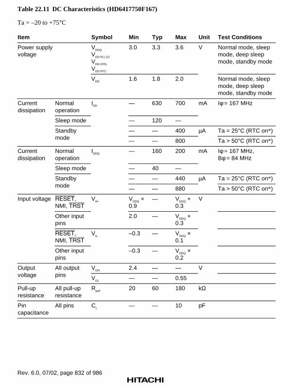
Rev. 6.0, 07/02, page 832 of 986
Table 22.11 DC Characteristics (HD6417750F167)
Ta = –20 to +75°C
Item Symbol Min Typ Max Unit Test Conditions
VDDQ
VDD-PLL1/2
VDD-CPG
VDD-RTC
3.0 3.3 3.6 V Normal mode, sleepmode, deep sleepmode, standby mode
Power supplyvoltage
VDD 1.6 1.8 2.0 Normal mode, sleepmode, deep sleepmode, standby mode
Normaloperation
— 630 700
Sleep mode — 120 —
mA Iφ = 167 MHz
— — 400 Ta = 25°C (RTC on*)
Currentdissipation
Standbymode
IDD
— — 800
µA
Ta > 50°C (RTC on*)
Normaloperation
— 160 200
Sleep mode — 40 —
mA Iφ = 167 MHz,Bφ = 84 MHz
— — 440 Ta = 25°C (RTC on*)
Currentdissipation
Standbymode
IDDQ
— — 880
µA
Ta > 50°C (RTC on*)
RESET,NMI, TRST
VIH VDDQ ×0.9
— VDDQ +0.3
V
Other inputpins
2.0 — VDDQ +0.3
RESET,NMI, TRST
VIL –0.3 — VDDQ ×0.1
Input voltage
Other inputpins
–0.3 — VDDQ ×0.2
VOH 2.4 — — VOutputvoltage
All outputpins VOL — — 0.55
Pull-upresistance
All pull-upresistance
Rpull 20 60 180 kΩ
Pincapacitance
All pins CL — — 10 pF

Rev. 6.0, 07/02, page 833 of 986
Notes: 1. Connect VDD-PLL1/2, VDD-RTC, and VDD-CPG to VDDQ, and VSS-CPG, VSS-PLL1/2, and VSSQ-RTC to GND,regardless of whether or not the PLL circuits and RTC are used.
2. The current dissipation values are for VIH min = VDDQ – 0.5 V and VIL max = 0.5 V with alloutput pins unloaded.
3. IDDQ is the sum of the VDDQ, VDD-PLL1/2, VDD-RTC, and VDD-CPG 3.3 V system currents.* To reduce the leakage current in standby mode, the RTC must be turned on (input the
clock from EXTAL2 and set RCR2.RTCEN to 1).
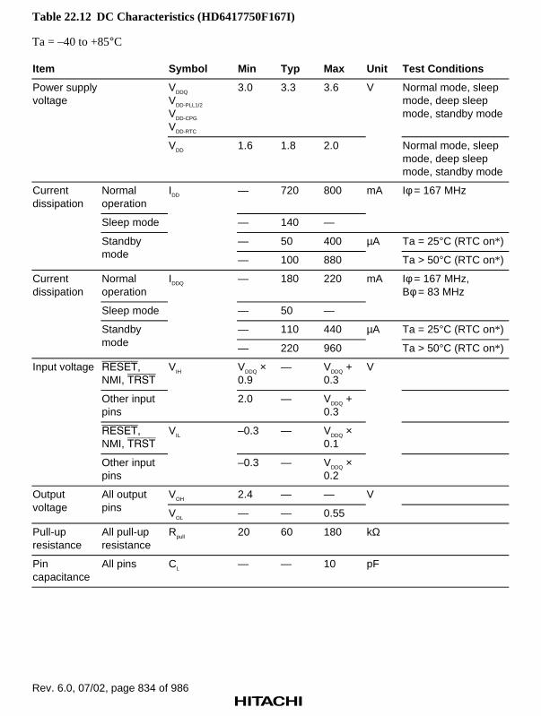
Rev. 6.0, 07/02, page 834 of 986
Table 22.12 DC Characteristics (HD6417750F167I)
Ta = –40 to +85°C
Item Symbol Min Typ Max Unit Test Conditions
VDDQ
VDD-PLL1/2
VDD-CPG
VDD-RTC
3.0 3.3 3.6 V Normal mode, sleepmode, deep sleepmode, standby mode
Power supplyvoltage
VDD 1.6 1.8 2.0 Normal mode, sleepmode, deep sleepmode, standby mode
Normaloperation
— 720 800
Sleep mode — 140 —
mA Iφ = 167 MHz
— 50 400 Ta = 25°C (RTC on*)
Currentdissipation
Standbymode
IDD
— 100 880
µA
Ta > 50°C (RTC on*)
Normaloperation
— 180 220
Sleep mode — 50 —
mA Iφ = 167 MHz,Bφ = 83 MHz
— 110 440 Ta = 25°C (RTC on*)
Currentdissipation
Standbymode
IDDQ
— 220 960
µA
Ta > 50°C (RTC on*)
RESET,NMI, TRST
VIH VDDQ ×0.9
— VDDQ +0.3
V
Other inputpins
2.0 — VDDQ +0.3
RESET,NMI, TRST
VIL –0.3 — VDDQ ×0.1
Input voltage
Other inputpins
–0.3 — VDDQ ×0.2
VOH 2.4 — — VOutputvoltage
All outputpins VOL — — 0.55
Pull-upresistance
All pull-upresistance
Rpull 20 60 180 kΩ
Pincapacitance
All pins CL — — 10 pF

Rev. 6.0, 07/02, page 835 of 986
Notes: 1. Connect VDD-PLL1/2, VDD-RTC, and VDD-CPG to VDDQ, and VSS-CPG, VSS-PLL1/2, and VSSQ-RTC to GND,regardless of whether or not the PLL circuits and RTC are used.
2. The current dissipation values are for VIH min = VDDQ – 0.5 V and VIL max = 0.5 V with alloutput pins unloaded.
3. IDDQ is the sum of the VDDQ, VDD-PLL1/2, VDD-RTC, and VDD-CPG 3.3 V system currents.* To reduce the leakage current in standby mode, the RTC must be turned on (input the
clock from EXTAL2 and set RCR2.RTCEN to 1).

Rev. 6.0, 07/02, page 836 of 986
Table 22.13 DC Characteristics (HD6417750SVF133)
Ta = –20 to +75°C
Item Symbol Min Typ Max Unit Test Conditions
VDDQ
VDD-PLL1/2
VDD-CPG
VDD-RTC
3.0 3.3 3.6 V Normal mode, sleepmode, deep sleepmode, standby mode
Power supplyvoltage
VDD 1.4 1.5 1.7 Normal mode, sleepmode, deep sleepmode, standby mode
Normaloperation
— 210 520
Sleep mode — 50 60
mA Iφ = 133 MHz,Bφ = 66 MHz
— — 100 Ta = 25°C (RTC on*)
Currentdissipation
Standbymode
IDD
— — 200
µA
Ta > 50°C (RTC on*)
Normaloperation
— 80 160
Sleep mode — 35 40
mA Iφ = 133 MHz,Bφ = 67 MHz
— — 110 Ta = 25°C (RTC on*)
Currentdissipation
Standbymode
IDDQ
— — 220
µA
Ta > 50°C (RTC on*)
RTC currentdissipation
During RTCoperation
IDD-RTC — 15 25 µA RTC input clock:32.768 kHz
Power is supplied onlyto VDD-RTC
RESET,NMI, TRST
VIH VDDQ ×0.9
— VDDQ +0.3
V
Other inputpins
2.0 — VDDQ +0.3
RESET,NMI, TRST
VIL –0.3 — VDDQ ×0.1
Input voltage
Other inputpins
–0.3 — VDDQ ×0.2
VOH 2.4 — — VOutputvoltage
All outputpins VOL — — 0.55
Pull-upresistance
All pull-upresistance
Rpull 20 60 180 kΩ
Pincapacitance
All pins CL — — 10 pF

Rev. 6.0, 07/02, page 837 of 986
Notes: 1. Connect VDD-PLL1/2, VDD-RTC, and VDD-CPG to VDDQ, and VSS-CPG, VSS-PLL1/2, and VSSQ-RTC to GND,regardless of whether or not the PLL circuits and RTC are used.
2. The current dissipation values are for VIH min = VDDQ – 0.5 V and VIL max = 0.5 V with alloutput pins unloaded.
3. IDDQ is the sum of the VDDQ, VDD-PLL1/2, VDD-RTC, and VDD-CPG 3.3 V system currents.* To reduce the leakage current in standby mode, the RTC must be turned on (input the
clock from EXTAL2 and set RCR2.RTCEN to 1).

Rev. 6.0, 07/02, page 838 of 986
Table 22.14 DC Characteristics (HD6417750SVBT133)
Ta = –30 to +70°C
Item Symbol Min Typ Max Unit Test Conditions
VDDQ
VDD-PLL1/2
VDD-CPG
VDD-RTC
3.0 3.3 3.6 V Normal mode, sleepmode, deep sleepmode, standby mode
Power supplyvoltage
VDD 1.4 1.5 1.7 Normal mode, sleepmode, deep sleepmode, standby mode
Normaloperation
— 210 520
Sleep mode — 50 60
mA Iφ = 133 MHz,Bφ = 66 MHz
— — 100 Ta = 25°C (RTC on*)
Currentdissipation
Standbymode
IDD
— — 200
µA
Ta > 50°C (RTC on*)
Normaloperation
— 80 160
Sleep mode — 35 40
mA Iφ = 133 MHz,Bφ = 67 MHz
— — 110 Ta = 25°C (RTC on*)
Currentdissipation
Standbymode
IDDQ
— — 220
µA
Ta > 50°C (RTC on*)
RTC currentdissipation
During RTCoperation
IDD-RTC — 15 45 µA RTC input clock:32.768 kHz
Power is supplied onlyto VDD-RTC
RESET,NMI, TRST
VIH VDDQ ×0.9
— VDDQ +0.3
V
Other inputpins
2.0 — VDDQ +0.3
RESET,NMI, TRST
VIL –0.3 — VDDQ ×0.1
Input voltage
Other inputpins
–0.3 — VDDQ ×0.2
VOH 2.4 — — VOutputvoltage
All outputpins VOL — — 0.55
Pull-upresistance
All pull-upresistance
Rpull 20 60 180 kΩ
Pincapacitance
All pins CL — — 10 pF

Rev. 6.0, 07/02, page 839 of 986
Notes: 1. Connect VDD-PLL1/2, VDD-RTC, and VDD-CPG to VDDQ, and VSS-CPG, VSS-PLL1/2, and VSSQ-RTC to GND,regardless of whether or not the PLL circuits and RTC are used.
2. The current dissipation values are for VIH min = VDDQ – 0.5 V and VIL max = 0.5 V with alloutput pins unloaded.
3. IDDQ is the sum of the VDDQ, VDD-PLL1/2, VDD-RTC, and VDD-CPG 3.3 V system currents.* To reduce the leakage current in standby mode, the RTC must be turned on (input the
clock from EXTAL2 and set RCR2.RTCEN to 1).

Rev. 6.0, 07/02, page 840 of 986
Table 22.15 DC Characteristics (HD6417750VF128)
Ta = –20 to +75°C
Item Symbol Min Typ Max Unit Test Conditions
VDDQ
VDD-PLL1/2
VDD-CPG
VDD-RTC
3.0 3.3 3.6 V Normal mode, sleepmode, deep sleepmode, standby mode
Power supplyvoltage
VDD 1.4 1.5 1.7 Normal mode, sleepmode, deep sleepmode, standby mode
Normaloperation
— — 520
Sleep mode — — 60
mA Iφ = 128 MHz,Bφ = 64 MHz
— — 100 Ta = 25°C (RTC on*)
Currentdissipation
Standbymode
IDD
— — 200
µA
Ta > 50°C (RTC on*)
Normaloperation
— — 160
Sleep mode — — 40
mA Iφ = 128 MHz,Bφ = 64 MHz
— — 110 Ta = 25°C (RTC on*)
Currentdissipation
Standbymode
IDDQ
— — 220
µA
Ta > 50°C (RTC on*)
RESET,NMI, TRST
VIH VDDQ ×0.9
— VDDQ +0.3
V
Other inputpins
2.0 — VDDQ +0.3
RESET,NMI, TRST
VIL –0.3 — VDDQ ×0.1
Input voltage
Other inputpins
–0.3 — VDDQ ×0.2
VOH 2.4 — — VOutputvoltage
All outputpins VOL — — 0.55
Pull-upresistance
All pull-upresistance
Rpull 20 60 180 kΩ
Pincapacitance
All pins CL — — 10 pF

Rev. 6.0, 07/02, page 841 of 986
Notes: 1. Connect VDD-PLL1/2, VDD-RTC, and VDD-CPG to VDDQ, and VSS-CPG, VSS-PLL1/2, and VSSQ-RTC to GND,regardless of whether or not the PLL circuits and RTC are used.
2. The current dissipation values are for VIH min = VDDQ – 0.5 V and VIL max = 0.5 V with alloutput pins unloaded.
3. IDDQ is the sum of the VDDQ, VDD-PLL1/2, VDD-RTC, and VDD-CPG 3.3 V system currents.* To reduce the leakage current in standby mode, the RTC must be turned on (input the
clock from EXTAL2 and set RCR2.RTCEN to 1).
Table 22.16 Permissible Output Currents
Ta = –20 to +75°C
Item Symbol Min Typ Max Unit
Permissible output low current(per pin)
IOL — — 2 mA
Permissible output low current(total)
ΣIOL — — 120
Permissible output high current(per pin)
–IOH — — 2
Permissible output high current(total)
Σ(–IOH) — — 40
Note: To protect chip reliability, do not exceed the output current values in table 22.16.
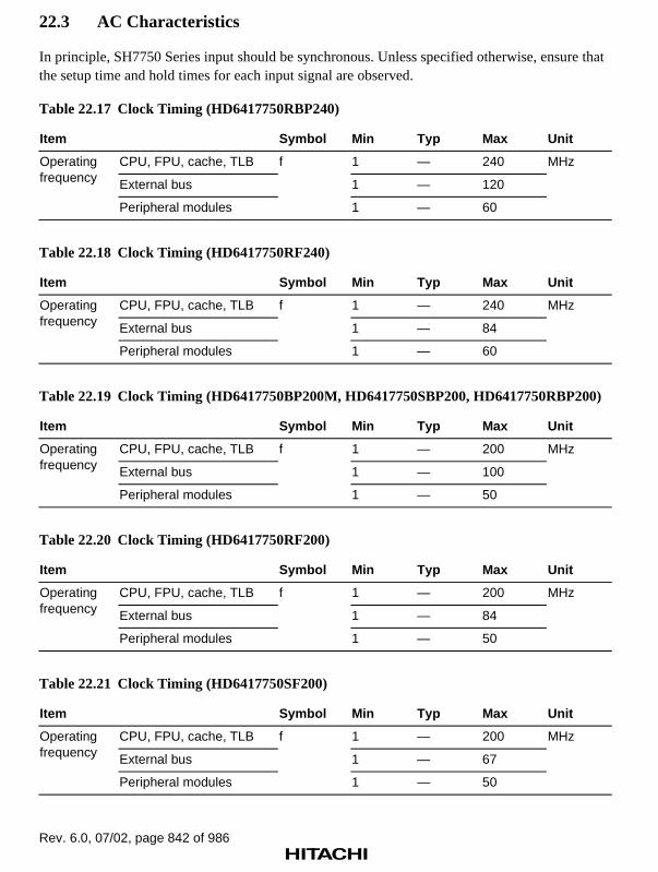
Rev. 6.0, 07/02, page 842 of 986
22.3 AC Characteristics
In principle, SH7750 Series input should be synchronous. Unless specified otherwise, ensure thatthe setup time and hold times for each input signal are observed.
Table 22.17 Clock Timing (HD6417750RBP240)
Item Symbol Min Typ Max Unit
CPU, FPU, cache, TLB 1 — 240
External bus 1 — 120
Operatingfrequency
Peripheral modules
f
1 — 60
MHz
Table 22.18 Clock Timing (HD6417750RF240)
Item Symbol Min Typ Max Unit
CPU, FPU, cache, TLB 1 — 240
External bus 1 — 84
Operatingfrequency
Peripheral modules
f
1 — 60
MHz
Table 22.19 Clock Timing (HD6417750BP200M, HD6417750SBP200, HD6417750RBP200)
Item Symbol Min Typ Max Unit
CPU, FPU, cache, TLB 1 — 200
External bus 1 — 100
Operatingfrequency
Peripheral modules
f
1 — 50
MHz
Table 22.20 Clock Timing (HD6417750RF200)
Item Symbol Min Typ Max Unit
CPU, FPU, cache, TLB 1 — 200
External bus 1 — 84
Operatingfrequency
Peripheral modules
f
1 — 50
MHz
Table 22.21 Clock Timing (HD6417750SF200)
Item Symbol Min Typ Max Unit
CPU, FPU, cache, TLB 1 — 200
External bus 1 — 67
Operatingfrequency
Peripheral modules
f
1 — 50
MHz

Rev. 6.0, 07/02, page 843 of 986
Table 22.22 Clock Timing (HD6417750F167, HD6417750F167I, HD6417750SF167,HD6417750SF167I)
Item Symbol Min Typ Max Unit
CPU, FPU, cache, TLB f 1 — 167
External bus 1 — 84
Operatingfrequency
Peripheral modules 1 — 42
MHz
Table 22.23 Clock Timing (HD6417750SVF133, HD6417750SVBT133)
Item Symbol Min Typ Max Unit
CPU, FPU, cache, TLB 1 — 134
External bus 1 — 67
Operatingfrequency
Peripheral modules
f
1 — 34
MHz
Table 22.24 Clock Timing (HD6417750VF128)
Item Symbol Min Typ Max Unit
CPU, FPU, cache, TLB 1 — 128
External bus 1 — 64
Operatingfrequency
Peripheral modules
f
1 — 32
MHz

Rev. 6.0, 07/02, page 844 of 986
22.3.1 Clock and Control Signal Timing
Table 22.25 Clock and Control Signal Timing (HD6417750RBP240)
VDDQ = 3.0 to 3.6 V, VDD = 1.5 V, Ta = –20 to +75°C, CL = 30 pF
Item Symbol Min Max Unit Figure
PLL1 6-times/PLL2operation
fEX 16 34 MHz
PLL1 12-times/PLL2operation
fEX 14 20
EXTALclock inputfrequency
PLL1/PLL2 not operating fEX 1 34
EXTAL clock input cycle time tEXcyc 30 1000 ns 22.1
EXTAL clock input low-level pulse width tEXL 3.5 — ns 22.1
EXTAL clock input high-level pulse width tEXH 3.5 — ns 22.1
EXTAL clock input rise time tEXr — 4 ns 22.1
EXTAL clock input fall time tEXf — 4 ns 22.1
PLL1/PLL2 operating fOP 25 120 MHzCKIO clockoutput PLL1/PLL2 not operating fOP 1 34 MHz
CKIO clock output cycle time tcyc 8.3 1000 ns 22.2(1)
CKIO clock output low-level pulse width tCKOL1 1 — ns 22.2(1)
CKIO clock output high-level pulse width tCKOH1 1 — ns 22.2(1)
CKIO clock output rise time tCKOr — 3 ns 22.2(1)
CKIO clock output fall time tCKOf — 3 ns 22.2(1)
CKIO clock output low-level pulse width tCKOL2 3 — ns 22.2(2)
CKIO clock output high-level pulse width tCKOH2 3 — ns 22.2(2)
Power-on oscillation settling time tOSC1 10 — ms 22.3, 22.5
Power-on oscillation settling time/modesettling
tOSCMD 10 — ms 22.3, 22.5
SCK2 reset setup time tSCK2RS 20 — ns 22.11
SCK2 reset hold time tSCK2RH 20 — ns 22.3, 22.5, 22.11
MD reset setup time tMDRS 3 — tcyc 22.12
MD reset hold time tMDRH 20 — ns 22.3, 22.5, 22.12
RESET assert time tRESW 20 — tcyc 22.3, 22.4, 22.5,22.6, 22.11
PLL synchronization settling time tPLL 200 — µs 22.9, 22.10
Standby return oscillation settling time 1 tOSC2 3 — ms 22.4, 22.6
Standby return oscillation settling time 2 tOSC3 3 — ms 22.7

Rev. 6.0, 07/02, page 845 of 986
Item Symbol Min Max Unit Figure
Standby return oscillation settling time 3 tOSC4 3 — ms 22.8
Standby return oscillation settling time 1* tOSC2 2 — ms
Standby return oscillation settling time 2* tOSC3 2 — ms
Standby return oscillation settling time 3* tOSC4 2 — ms
IRL interrupt determination time(RTC used, standby mode)
tIRLSTB — 200 µs 22.10
TRST reset hold time tTRSTRH 0 — ns 22.3, 22.5
Notes: 1. When a crystal resonator is connected to EXTAL and XTAL, the maximum frequency is34 MHz. When a 3rd overtone crystal resonator is used, an external tank circuit isnecessary.
2. The maximum load capacitance to be connected to CKIO pin should be 50 pF in PLL2operation, because there is a feedback from CKIO pin.
* When the oscillation settling time of a crystal resonator is lower than or equal to 1 ms.

Rev. 6.0, 07/02, page 846 of 986
Table 22.26 Clock and Control Signal Timing (HD6417750RF240)
VDDQ = 3.0 to 3.6 V, VDD = 1.5 V, Ta = –20 to +75°C, CL = 30 pF
Item Symbol Min Max Unit Figure
PLL1 6-times/PLL2operation
fEX 16 34 MHz
PLL1 12-times/PLL2operation
fEX 14 20
EXTALclock inputfrequency
PLL1/PLL2 not operating fEX 1 34
EXTAL clock input cycle time tEXcyc 30 1000 ns 22.1
EXTAL clock input low-level pulse width tEXL 3.5 — ns 22.1
EXTAL clock input high-level pulse width tEXH 3.5 — ns 22.1
EXTAL clock input rise time tEXr — 4 ns 22.1
EXTAL clock input fall time tEXf — 4 ns 22.1
PLL1/PLL2 operating fOP 25 84 MHzCKIO clockoutput PLL1/PLL2 not operating fOP 1 34 MHz
CKIO clock output cycle time tcyc 11.9 1000 ns 22.2(1)
CKIO clock output low-level pulse width tCKOL1 1 — ns 22.2(1)
CKIO clock output high-level pulse width tCKOH1 1 — ns 22.2(1)
CKIO clock output rise time tCKOr — 3 ns 22.2(1)
CKIO clock output fall time tCKOf — 3 ns 22.2(1)
CKIO clock output low-level pulse width tCKOL2 3 — ns 22.2(2)
CKIO clock output high-level pulse width tCKOH2 3 — ns 22.2(2)
Power-on oscillation settling time tOSC1 10 — ms 22.3, 22.5
Power-on oscillation settling time/modesettling
tOSCMD 10 — ms 22.3, 22.5
SCK2 reset setup time tSCK2RS 20 — ns 22.11
SCK2 reset hold time tSCK2RH 20 — ns 22.3, 22.5, 22.11
MD reset setup time tMDRS 3 — tcyc 22.12
MD reset hold time tMDRH 20 — ns 22.3, 22.5, 22.12
RESET assert time tRESW 20 — tcyc 22.3, 22.4, 22.5,22.6, 22.11
PLL synchronization settling time tPLL 200 — µs 22.9, 22.10
Standby return oscillation settling time 1 tOSC2 3 — ms 22.4, 22.6
Standby return oscillation settling time 2 tOSC3 3 — ms 22.7
Standby return oscillation settling time 3 tOSC4 3 — ms 22.8

Rev. 6.0, 07/02, page 847 of 986
Item Symbol Min Max Unit Figure
Standby return oscillation settling time 1* tOSC2 2 — ms
Standby return oscillation settling time 2* tOSC3 2 — ms
Standby return oscillation settling time 3* tOSC4 2 — ms
IRL interrupt determination time(RTC used, standby mode)
tIRLSTB — 200 µs 22.10
TRST reset hold time tTRSTRH 0 — ns 22.3, 22.5
Notes: 1. When a crystal resonator is connected to EXTAL and XTAL, the maximum frequency is34 MHz. When a 3rd overtone crystal resonator is used, an external tank circuit isnecessary.
2. The maximum load capacitance to be connected to CKIO pin should be 50 pF in PLL2operation, because there is a feedback from CKIO pin.
* When the oscillation settling time of a crystal resonator is lower than or equal to 1 ms.
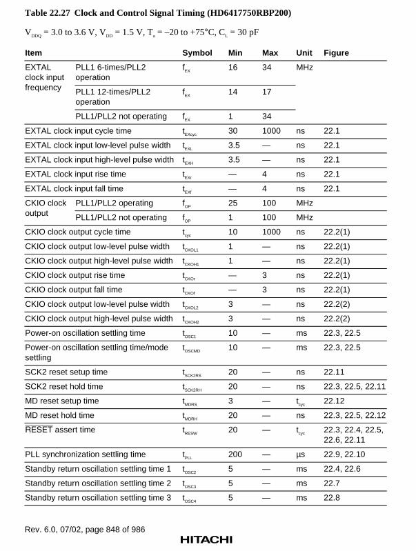
Rev. 6.0, 07/02, page 848 of 986
Table 22.27 Clock and Control Signal Timing (HD6417750RBP200)
VDDQ = 3.0 to 3.6 V, VDD = 1.5 V, Ta = –20 to +75°C, CL = 30 pF
Item Symbol Min Max Unit Figure
PLL1 6-times/PLL2operation
fEX 16 34 MHzEXTALclock inputfrequency PLL1 12-times/PLL2
operationfEX 14 17
PLL1/PLL2 not operating fEX 1 34
EXTAL clock input cycle time tEXcyc 30 1000 ns 22.1
EXTAL clock input low-level pulse width tEXL 3.5 — ns 22.1
EXTAL clock input high-level pulse width tEXH 3.5 — ns 22.1
EXTAL clock input rise time tEXr — 4 ns 22.1
EXTAL clock input fall time tEXf — 4 ns 22.1
PLL1/PLL2 operating fOP 25 100 MHzCKIO clockoutput PLL1/PLL2 not operating fOP 1 100 MHz
CKIO clock output cycle time tcyc 10 1000 ns 22.2(1)
CKIO clock output low-level pulse width tCKOL1 1 — ns 22.2(1)
CKIO clock output high-level pulse width tCKOH1 1 — ns 22.2(1)
CKIO clock output rise time tCKOr — 3 ns 22.2(1)
CKIO clock output fall time tCKOf — 3 ns 22.2(1)
CKIO clock output low-level pulse width tCKOL2 3 — ns 22.2(2)
CKIO clock output high-level pulse width tCKOH2 3 — ns 22.2(2)
Power-on oscillation settling time tOSC1 10 — ms 22.3, 22.5
Power-on oscillation settling time/modesettling
tOSCMD 10 — ms 22.3, 22.5
SCK2 reset setup time tSCK2RS 20 — ns 22.11
SCK2 reset hold time tSCK2RH 20 — ns 22.3, 22.5, 22.11
MD reset setup time tMDRS 3 — tcyc 22.12
MD reset hold time tMDRH 20 — ns 22.3, 22.5, 22.12
RESET assert time tRESW 20 — tcyc 22.3, 22.4, 22.5,22.6, 22.11
PLL synchronization settling time tPLL 200 — µs 22.9, 22.10
Standby return oscillation settling time 1 tOSC2 5 — ms 22.4, 22.6
Standby return oscillation settling time 2 tOSC3 5 — ms 22.7
Standby return oscillation settling time 3 tOSC4 5 — ms 22.8

Rev. 6.0, 07/02, page 849 of 986
Item Symbol Min Max Unit Figure
Standby return oscillation settling time 1* tOSC2 2 — ms
Standby return oscillation settling time 2* tOSC3 2 — ms
Standby return oscillation settling time 3* tOSC4 2 — ms
IRL interrupt determination time(RTC used, standby mode)
tIRLSTB — 200 µs 22.10
TRST reset hold time tTRSTRH 0 — ns 22.3, 22.5
Notes: 1. When a crystal resonator is connected to EXTAL and XTAL, the maximum frequency is34 MHz. When a 3rd overtone crystal resonator is used, an external tank circuit isnecessary.
2. The maximum load capacitance to be connected to CKIO pin should be 50 pF in PLL2operation, because there is a feedback from CKIO pin.
* When the oscillation settling time of a crystal resonator is lower than or equal to 1 ms.

Rev. 6.0, 07/02, page 850 of 986
Table 22.28 Clock and Control Signal Timing (HD6417750RF200)
VDDQ = 3.0 to 3.6 V, VDD = 1.5 V, Ta = –20 to +75°C, CL = 30 pF
Item Symbol Min Max Unit Figure
PLL1 6-times/PLL2operation
fEX 16 34 MHzEXTALclock inputfrequency PLL1 12-times/PLL2
operationfEX 14 17
PLL1/PLL2 not operating fEX 1 34
EXTAL clock input cycle time tEXcyc 30 1000 ns 22.1
EXTAL clock input low-level pulse width tEXL 3.5 — ns 22.1
EXTAL clock input high-level pulse width tEXH 3.5 — ns 22.1
EXTAL clock input rise time tEXr — 4 ns 22.1
EXTAL clock input fall time tEXf — 4 ns 22.1
PLL1/PLL2 operating fOP 25 84 MHzCKIO clockoutput PLL1/PLL2 not operating fOP 1 34 MHz
CKIO clock output cycle time tcyc 11.9 1000 ns 22.2(1)
CKIO clock output low-level pulse width tCKOL1 1 — ns 22.2(1)
CKIO clock output high-level pulse width tCKOH1 1 — ns 22.2(1)
CKIO clock output rise time tCKOr — 3 ns 22.2(1)
CKIO clock output fall time tCKOf — 3 ns 22.2(1)
CKIO clock output low-level pulse width tCKOL2 3 — ns 22.2(2)
CKIO clock output high-level pulse width tCKOH2 3 — ns 22.2(2)
Power-on oscillation settling time tOSC1 10 — ms 22.3, 22.5
Power-on oscillation settling time/modesettling
tOSCMD 10 — ms 22.3, 22.5
SCK2 reset setup time tSCK2RS 20 — ns 22.11
SCK2 reset hold time tSCK2RH 20 — ns 22.3, 22.5, 22.11
MD reset setup time tMDRS 3 — tcyc 22.12
MD reset hold time tMDRH 20 — ns 22.3, 22.5, 22.12
RESET assert time tRESW 20 — tcyc 22.3, 22.4, 22.5,22.6, 22.11
PLL synchronization settling time tPLL 200 — µs 22.9, 22.10
Standby return oscillation settling time 1 tOSC2 5 — ms 22.4, 22.6
Standby return oscillation settling time 2 tOSC3 5 — ms 22.7
Standby return oscillation settling time 3 tOSC4 5 — ms 22.8

Rev. 6.0, 07/02, page 851 of 986
Item Symbol Min Max Unit Figure
Standby return oscillation settling time 1* tOSC2 2 — ms
Standby return oscillation settling time 2* tOSC3 2 — ms
Standby return oscillation settling time 3* tOSC4 2 — ms
IRL interrupt determination time(RTC used, standby mode)
tIRLSTB — 200 µs 22.10
TRST reset hold time tTRSTRH 0 — ns 22.3, 22.5
Notes: 1. When a crystal resonator is connected to EXTAL and XTAL, the maximum frequency is34 MHz. When a 3rd overtone crystal resonator is used, an external tank circuit isnecessary.
2. The maximum load capacitance to be connected to CKIO pin should be 50 pF in PLL2operation, because there is a feedback from CKIO pin.
* When the oscillation settling time of a crystal resonator is lower than or equal to 1 ms.

Rev. 6.0, 07/02, page 852 of 986
Table 22.29 Clock and Control Signal Timing (HD6417750BP200M, HD6417750SBP200)
VDDQ = 3.0 to 3.6 V, VDD = 1.5 V, Ta = –20 to +75°C, CL = 30 pF
Item Symbol Min Max Unit Figure
1/2 divideroperating
fEX 16 67 MHzPLL2operating
1/2 divider notoperating
fEX 8 34
1/2 divideroperating
fEX 2 67
EXTALclock inputfrequency
PLL2 notoperating
1/2 divider notoperating
fEX 1 34
EXTAL clock input cycle time tEXcyc 15 1000 ns 22.1
EXTAL clock input low-level pulse width tEXL 3.5 — ns 22.1
EXTAL clock input high-level pulse width tEXH 3.5 — ns 22.1
EXTAL clock input rise time tEXr — 4 ns 22.1
EXTAL clock input fall time tEXf — 4 ns 22.1
PLL2 operating fOP 25 100 MHzCKIO clockoutput PLL2 not operating fOP 1 100 MHz
CKIO clock output cycle time tcyc 10 1000 ns 22.2(1)
CKIO clock output low-level pulse width tCKOL1 1 — ns 22.2(1)
CKIO clock output high-level pulse width tCKOH1 1 — ns 22.2(1)
CKIO clock output rise time tCKOr — 3 ns 22.2(1)
CKIO clock output fall time tCKOf — 3 ns 22.2(1)
CKIO clock output low-level pulse width tCKOL2 3 — ns 22.2(2)
CKIO clock output high-level pulse width tCKOH2 3 — ns 22.2(2)
Power-on oscillation settling time tOSC1 10 — ms 22.3, 22.5
Power-on oscillation settling time/modesettling
tOSCMD 10 — ms 22.3, 22.5
SCK2 reset setup time tSCK2RS 20 — ns 22.11
SCK2 reset hold time tSCK2RH 20 — ns 22.3, 22.5, 22.11
MD reset setup time tMDRS 3 — tcyc 22.12
MD reset hold time tMDRH 20 — ns 22.3, 22.5, 22.12
RESET assert time tRESW 20 — tcyc 22.3, 22.4, 22.5,22.6, 22.11
PLL synchronization settling time tPLL 200 — µs 22.9, 22.10

Rev. 6.0, 07/02, page 853 of 986
Item Symbol Min Max Unit Figure
Standby return oscillation settling time 1 tOSC2 10 — ms 22.4, 22.6
Standby return oscillation settling time 2 tOSC3 5 — ms 22.7
Standby return oscillation settling time 3 tOSC4 5 — ms 22.8
Standby return oscillation settling time 1* tOSC2 2 — ms
Standby return oscillation settling time 2* tOSC3 2 — ms
Standby return oscillation settling time 3* tOSC4 2 — ms
IRL interrupt determination time(RTC used, standby mode)
tIRLSTB — 200 µs 22.10
TRST reset hold time tTRSTRH 0 — ns 22.3, 22.5
Notes: 1. When a crystal resonator is connected to EXTAL and XTAL, the maximum frequency is34 MHz. When a 3rd overtone crystal resonator is used, an external tank circuit isnecessary.
2. The maximum load capacitance to be connected to CKIO pin should be 50 pF in PLL2operation, because there is a feedback from CKIO pin.
* When the oscillation settling time of a crystal resonator is lower than or equal to 1 ms.

Rev. 6.0, 07/02, page 854 of 986
Table 22.30 Clock and Control Signal Timing (HD6417750SF200)
VDDQ = 3.0 to 3.6 V, VDD = 1.8 V, Ta = –20 to +75°C, CL = 30 pF
Item Symbol Min Max Unit Figure
1/2 divideroperating
fEX 16 67 MHzPLL2operating
1/2 divider notoperating
fEX 8 34
1/2 divideroperating
fEX 2 67
EXTALclock inputfrequency
PLL2 notoperating
1/2 divider notoperating
fEX 1 34
EXTAL clock input cycle time tEXcyc 15 1000 ns 22.1
EXTAL clock input low-level pulse width tEXL 3.5 — ns 22.1
EXTAL clock input high-level pulse width tEXH 3.5 — ns 22.1
EXTAL clock input rise time tEXr — 4 ns 22.1
EXTAL clock input fall time tEXf — 4 ns 22.1
PLL2 operating fOP 25 67 MHzCKIO clockoutput PLL2 not operating fOP 1 67 MHz
CKIO clock output cycle time tcyc 10 1000 ns 22.2(1)
CKIO clock output low-level pulse width tCKOL1 1 — ns 22.2(1)
CKIO clock output high-level pulse width tCKOH1 1 — ns 22.2(1)
CKIO clock output rise time tCKOr — 3 ns 22.2(1)
CKIO clock output fall time tCKOf — 3 ns 22.2(1)
CKIO clock output low-level pulse width tCKOL2 3 — ns 22.2(2)
CKIO clock output high-level pulse width tCKOH2 3 — ns 22.2(2)
Power-on oscillation settling time tOSC1 10 — ms 22.3, 22.5
Power-on oscillation settling time/modesettling
tOSCMD 10 — ms 22.3, 22.5
SCK2 reset setup time tSCK2RS 20 — ns 22.11
SCK2 reset hold time tSCK2RH 20 — ns 22.3, 22.5, 22.11
MD reset setup time tMDRS 3 — tcyc 22.12
MD reset hold time tMDRH 20 — ns 22.3, 22.5, 22.12
RESET assert time tRESW 20 — tcyc 22.3, 22.4, 22.5,22.6, 22.11
PLL synchronization settling time tPLL 200 — µs 22.9, 22.10

Rev. 6.0, 07/02, page 855 of 986
Item Symbol Min Max Unit Figure
Standby return oscillation settling time 1 tOSC2 10 — ms 22.4, 22.6
Standby return oscillation settling time 2 tOSC3 5 — ms 22.7
Standby return oscillation settling time 3 tOSC4 5 — ms 22.8
Standby return oscillation settling time 1* tOSC2 2 — ms
Standby return oscillation settling time 2* tOSC3 2 — ms
Standby return oscillation settling time 3* tOSC4 2 — ms
IRL interrupt determination time(RTC used, standby mode)
tIRLSTB — 200 µs 22.10
TRST reset hold time tTRSTRH 0 — ns 22.3, 22.5
Notes: 1. When a crystal resonator is connected to EXTAL and XTAL, the maximum frequency is34 MHz. When a 3rd overtone crystal resonator is used, an external tank circuit isnecessary.
2. The maximum load capacitance to be connected to CKIO pin should be 50 pF in PLL2operation, because there is a feedback from CKIO pin.
* When the oscillation settling time of a crystal resonator is lower than or equal to 1 ms.

Rev. 6.0, 07/02, page 856 of 986
Table 22.31 Clock and Control Signal Timing (HD6417750F167, HD6417750F167I,HD6417750SF167, HD6417750SF167I)
HD6417750SF167, HD6417750F167: VDDQ = 3.0 to 3.6 V, VDD = 1.8 V, Ta = –20 to +75°C,CL = 30 pF
HD6417750SF167I, HD6417750F167I: VDDQ = 3.0 to 3.6 V, VDD = 1.8 V, Ta = –40 to +85°C,CL = 30 pF
Item Symbol Min Max Unit Figure
1/2 divideroperating
fEX 16 56 MHzPLL2operating
1/2 divider notoperating
fEX 8 28
1/2 divideroperating
fEX 2 56
EXTALclock inputfrequency
PLL2 notoperating
1/2 divider notoperating
fEX 1 28
EXTAL clock input cycle time tEXcyc 18 1000 ns 22.1
EXTAL clock input low-level pulse width tEXL 3.5 — ns 22.1
EXTAL clock input high-level pulse width tEXH 3.5 — ns 22.1
EXTAL clock input rise time tEXr — 4 ns 22.1
EXTAL clock input fall time tEXf — 4 ns 22.1
PLL2 operating fOP 25 84 MHzCKIO clockoutput PLL2 not operating fOP 1 84 MHz
CKIO clock output cycle time tcyc 12 1000 ns 22.2(1)
CKIO clock output low-level pulse width tCKOL1 1 — ns 22.2(1)
CKIO clock output high-level pulse width tCKOH1 1 — ns 22.2(1)
CKIO clock output rise time tCKOr — 3 ns 22.2(1)
CKIO clock output fall time tCKOf — 3 ns 22.2(1)
CKIO clock output low-level pulse width tCKOL2 3 — ns 22.2(2)
CKIO clock output high-level pulse width tCKOH2 3 — ns 22.2(2)
Power-on oscillation settling time tOSC1 10 — ms 22.3, 22.5
Power-on oscillation settling time/modesettling
tOSCMD 10 — ms 22.3, 22.5
SCK2 reset setup time tSCK2RS 20 — ns 22.11
SCK2 reset hold time tSCK2RH 20 — ns 22.3, 22.5, 22.11
MD reset setup time tMDRS 3 — tcyc 22.12
MD reset hold time tMDRH 20 — ns 22.3, 22.5, 22.12

Rev. 6.0, 07/02, page 857 of 986
Item Symbol Min Max Unit Figure
RESET assert time tRESW 20 — tcyc 22.3, 22.4, 22.5,22.6, 22.11
PLL synchronization settling time tPLL 200 — µs 22.9, 22.10
Standby return oscillation settling time 1 tOSC2 10 — ms 22.4, 22.6
Standby return oscillation settling time 2 tOSC3 5 — ms 22.7
Standby return oscillation settling time 3 tOSC4 5 — ms 22.8
Standby return oscillation settling time 1* tOSC2 2 — ms
Standby return oscillation settling time 2* tOSC3 2 — ms
Standby return oscillation settling time 3* tOSC4 2 — ms
IRL interrupt determination time(RTC used, standby mode)
tIRLSTB — 200 µs 22.10
TRST reset hold time tTRSTRH 0 — ns 22.3, 22.5
Notes: 1. When a crystal resonator is connected to EXTAL and XTAL, the maximum frequency is28 MHz. When a 3rd overtone crystal resonator is used, an external tank circuit isnecessary.
2. The maximum load capacitance to be connected to CKIO pin should be 50 pF in PLL2operation, because there is a feedback from CKIO pin.
* When the oscillation settling time of a crystal resonator is lower than or equal to 1 ms.

Rev. 6.0, 07/02, page 858 of 986
Table 22.32 Clock and Control Signal Timing (HD6417750SVF133, HD6417750SVBT133)
HD6417750SVBT133: VDDQ = 3.0 to 3.6 V, VDD = 1.5 V typ, Ta = –30 to +70°C, CL = 30 pFHD6417750SVF133: VDDQ = 3.0 to 3.6 V, VDD = 1.5 V, Ta = –20 to +75°C, CL = 30 pF
Item Symbol Min Max Unit Figure
1/2 divideroperating
fEX 16 45 MHzPLL2operating
1/2 divider notoperating
fEX 8 23
1/2 divideroperating
fEX 2 45
EXTALclock inputfrequency
PLL2 notoperating
1/2 divider notoperating
fEX 1 23
EXTAL clock input cycle time tEXcyc 22 1000 ns 22.1
EXTAL clock input low-level pulse width tEXL 3.5 — ns 22.1
EXTAL clock input high-level pulse width tEXH 3.5 — ns 22.1
EXTAL clock input rise time tEXr — 4 ns 22.1
EXTAL clock input fall time tEXf — 4 ns 22.1
PLL2 operating fOP 25 67 MHzCKIO clockoutput PLL2 not operating fOP 1 67 MHz
CKIO clock output cycle time tcyc 14 1000 ns 22.2(1)
CKIO clock output low-level pulse width tCKOL1 1 — ns 22.2(1)
CKIO clock output high-level pulse width tCKOH1 1 — ns 22.2(1)
CKIO clock output rise time tCKOr — 3 ns 22.2(1)
CKIO clock output fall time tCKOf — 3 ns 22.2(1)
CKIO clock output low-level pulse width tCKOL2 3 — ns 22.2(2)
CKIO clock output high-level pulse width tCKOH2 3 — ns 22.2(2)
Power-on oscillation settling time tOSC1 10 — ms 22.3, 22.5
Power-on oscillation settling time/modesettling
tOSCMD 10 — ms 22.3, 22.5
SCK2 reset setup time tSCK2RS 20 — ns 22.11
SCK2 reset hold time tSCK2RH 20 — ns 22.3, 22.5, 22.11
MD reset setup time tMDRS 3 — tcyc 22.12
MD reset hold time tMDRH 20 — ns 22.3, 22.5, 22.12
RESET assert time tRESW 20 — tcyc 22.3, 22.4, 22.5,22.6, 22.11
PLL synchronization settling time tPLL 200 — µs 22.9, 22.10

Rev. 6.0, 07/02, page 859 of 986
Item Symbol Min Max Unit Figure
Standby return oscillation settling time 1 tOSC2 10 — ms 22.4, 22.6
Standby return oscillation settling time 2 tOSC3 5 — ms 22.7
Standby return oscillation settling time 3 tOSC4 5 — ms 22.8
Standby return oscillation settling time 1* tOSC2 2 — ms
Standby return oscillation settling time 2* tOSC3 2 — ms
Standby return oscillation settling time 3* tOSC4 2 — ms
IRL interrupt determination time(RTC used, standby mode)
tIRLSTB — 200 µs 22.10
TRST reset hold time tTRSTRH 0 — ns 22.3, 22.5
Notes: 1. When a crystal resonator is connected to EXTAL and XTAL, the maximum frequency is23 MHz. When a 3rd overtone crystal resonator is used, an external tank circuit isnecessary.
2. The maximum load capacitance to be connected to CKIO pin should be 50 pF in PLL2operation, because there is a feedback from CKIO pin.
* When the oscillation settling time of a crystal resonator is lower than or equal to 1 ms.

Rev. 6.0, 07/02, page 860 of 986
Table 22.33 Clock and Control Signal Timing (HD6417750VF128)
VDDQ = 3.0 to 3.6 V, VDD = 1.5 V, Ta = –20 to +75°C, CL = 30 pF
Item Symbol Min Max Unit Figure
1/2 divideroperating
fEX 16 43 MHzPLL2operating
1/2 divider notoperating
fEX 8 22
1/2 divideroperating
fEX 2 43
EXTALclock inputfrequency
PLL2notoperating 1/2 divider not
operatingfEX 1 22
EXTAL clock input cycle time tEXcyc 23 1000 ns 22.1
EXTAL clock input low-level pulse width tEXL 3.5 — ns 22.1
EXTAL clock input high-level pulse width tEXH 3.5 — ns 22.1
EXTAL clock input rise time tEXr — 4 ns 22.1
EXTAL clock input fall time tEXf — 4 ns 22.1
PLL2 operating fOP 25 64 MHzCKIO clockoutput PLL2 not operating fOP 1 64 MHz
CKIO clock output cycle time tcyc 15 1000 ns 22.2(1)
CKIO clock output low-level pulse width tCKOL1 1 — ns 22.2(1)
CKIO clock output high-level pulse width tCKOH1 1 — ns 22.2(1)
CKIO clock output rise time tCKOr — 3 ns 22.2(1)
CKIO clock output fall time tCKOf — 3 ns 22.2(1)
CKIO clock output low-level pulse width tCKOL2 3 — ns 22.2(2)
CKIO clock output high-level pulse width tCKOH2 3 — ns 22.2(2)
Power-on oscillation settling time tOSC1 10 — ms 22.3, 22.5
Power-on oscillation settling time/modesettling
tOSCMD 10 — ms 22.3, 22.5
SCK2 reset setup time tSCK2RS 20 — ns 22.11
SCK2 reset hold time tSCK2RH 20 — ns 22.3, 22.5, 22.11
MD reset setup time tMDRS 3 — tcyc 22.12
MD reset hold time tMDRH 20 — ns 22.3, 22.5, 22.12
RESET assert time tRESW 20 — tcyc 22.3, 22.4, 22.5,22.6, 22.11
PLL synchronization settling time tPLL 200 — µs 22.9, 22.10

Rev. 6.0, 07/02, page 861 of 986
Item Symbol Min Max Unit Figure
Standby return oscillation settling time 1 tOSC2 10 — ms 22.4, 22.6
Standby return oscillation settling time 2 tOSC3 5 — ms 22.7
Standby return oscillation settling time 3 tOSC4 5 — ms 22.8
Standby return oscillation settling time 1* tOSC2 2 — ms
Standby return oscillation settling time 2* tOSC3 2 — ms
Standby return oscillation settling time 3* tOSC4 2 — ms
IRL interrupt determination time(RTC used, standby mode)
tIRLSTB — 200 µs 22.10
TRST reset hold time tTRSTRH 0 — ns 22.3, 22.5
Notes: 1. When a crystal resonator is connected to EXTAL and XTAL, the maximum frequency is22 MHz. When a 3rd overtone crystal resonator is used, an external tank circuit isnecessary.
2. The maximum load capacitance to be connected to CKIO pin should be 50 pF in PLL2operation, because there is a feedback from CKIO pin.
* When the oscillation settling time of a crystal resonator is lower than or equal to 1 ms.

Rev. 6.0, 07/02, page 862 of 986
tEXcyc
tEXH tEXL
tEXrtEXf
1/2VDDQ
VIH VIH
VIL VIL
VIH
1/2VDDQ
Note: When the clock is input from the EXTAL pin
Figure 22.1 EXTAL Clock Input Timing
tcyc
tCKOH1 tCKOL1
tCKOrtCKOf
1/2VDDQ
VOH VOH
VOL VOL
VOH
1/2VDDQ
Figure 22.2(1) CKIO Clock Output Timing
tCKOH2 tCKOL2
1.5 V 1.5 V 1.5 V
Figure 22.2(2) CKIO Clock Output Timing

Rev. 6.0, 07/02, page 863 of 986
CKIO,internal clock
VDD
MD8, MD7,MD2–MD0
SCK2
tOSC1
VDD min
tSCK2RH
tMDRHtOSCMD
tTRSTRH
Stable oscillation
tRESW
Notes: 1. Oscillation settling time when on-chip resonator is used2. PLL2 not operating
Figure 22.3 Power-On Oscillation Settling Time
tRESW
tOSC2
Standby Stable oscillation
CKIO, internal clock
Notes: 1. Oscillation settling time when on-chip resonator is used2. PLL2 not operating
Figure 22.4 Standby Return Oscillation Settling Time (Return by RESETRESETRESETRESET)

Rev. 6.0, 07/02, page 864 of 986
Internal clock
VDD
MD8, MD7,MD2–MD0
SCK2
tOSC1
VDD min
tSCK2RH
tMDRHtOSCMD
tTRSTRH
Stable oscillation
tRESW
CKIO
Notes: 1. Oscillation settling time when on-chip resonator is used2. PLL2 operating
Figure 22.5 Power-On Oscillation Settling Time
tRESWtOSC2
CKIO
Stable oscillationStandby
Internalclock
Notes: 1. Oscillation settling time when on-chip resonator is used2. PLL2 operating
Figure 22.6 Standby Return Oscillation Settling Time (Return by RESETRESETRESETRESET)

Rev. 6.0, 07/02, page 865 of 986
CKIO, internal clock
NMI
Stable oscillationStandby
tOSC3
Note: Oscillation settling time when on-chip resonator is used
Figure 22.7 Standby Return Oscillation Settling Time (Return by NMI)
–
tOSC4
Standby Stable oscillation
CKIO, internal clock
Note: Oscillation settling time when on-chip resonator is used
Figure 22.8 Standby Return Oscillation Settling Time (Return by IRL3IRL3IRL3IRL3–IRL0IRL0IRL0IRL0)

Rev. 6.0, 07/02, page 866 of 986
EXTAL input
PLL output, CKIO output
Internal clock
STATUS1–STATUS0
Note: When external clock from EXTAL is input
Stable input clock
Normal Standby Normal
tPLL × 2
Stable input clock
Reset or NMI interrupt request
PLL synchronizationPLL synchronization
Figure 22.9 PLL Synchronization Settling Time in Case of RESETRESETRESETRESET or NMI Interrupt
–interrupt request
tIRLSTB
STATUS1–STATUS0
Note: When external clock from EXTAL is input
Normal Standby Normal
tPLL × 2
EXTAL input
PLL output, CKIO output
Internal clock
Stable input clock Stable input clock
PLL synchronizationPLL synchronization
Figure 22.10 PLL Synchronization Settling Time in Case of IRL Interrupt

Rev. 6.0, 07/02, page 867 of 986
CKIO
SCK2
tSCK2RS tSCK2RH
tRESW
Figure 22.11 Manual Reset Input Timing
tMDRS tMDRH
MD6–MD3
Figure 22.12 Mode Input Timing

Rev. 6.0, 07/02, page 868 of 986
22.3.2 Control Signal Timing
Table 22.34 Control Signal Timing (1)
HD6417750RBP240
HD6417750RBP200
HD6417750RF240
HD6417750RF200
* * * *
Item Symbol Min Max Min Max Min Max Min Max Unit Figure Notes
BREQ setuptime
tBREQS 2 — 2.5 — 3.5 — 3.5 — ns 22.13
BREQ holdtime
tBREQH 1.5 — 1.5 — 1.5 — 1.5 — ns 22.13
BACK delaytime
tBACKD — 5.3 — 6 — 6 — 6 ns 22.13
Bus tri-statedelay time
tBOFF1 — 12 — 12 — 12 — 12 ns 22.13
Bus tri-statedelay timeto standbymode
tBOFF2 — 2 — 2 — 2 — 2 tcyc 22.14
Bus bufferon time
tBON1 — 12 — 12 — 12 — 12 ns 22.13
Bus bufferon time fromstandby
tBON2 — 1 — 1 — 1 — 1 tcyc 22.14
STATUS0/1delay time
tSTD1 — 5 — 6 — 6 — 6 ns 22.14
STATUS0/1delay timeto standby
tSTD2 — 2 — 2 — 2 — 2 tcyc 22.14
Note: * VDDQ = 3.0 to 3.6 V, VDD = typ. 1.5 V, Ta = –20 to +75°C, CL = 30 pF, PLL2 on

Rev. 6.0, 07/02, page 869 of 986
Table 22.34 Control Signal Timing (2)
HD6417750VF128
HD6417750SVF133
HD6417750SVBT133
HD6417750F167
HD6417750F167I
HD6417750SF167
HD6417750SF167I
HD6417750SF200
HD6417750BP200M
HD6417750SBP200
*1 *1 *2 *3
Item Symbol Min Max Min Max Min Max Min Max Unit Figure Notes
BREQ setuptime
tBREQS 3.5 — 3.5 — 3.5 — 3 — ns 22.13
BREQ holdtime
tBREQH 1.5 — 1.5 — 1.5 — 1.5 — ns 22.13
BACK delaytime
tBACKD — 10 — 10 — 8 — 6 ns 22.13
Bus tri-statedelay time
tBOFF1 — 15 — 15 — 12 — 10 ns 22.13
Bus tri-statedelay timeto standbymode
tBOFF2 — 2 — 2 — 2 — 2 tcyc 22.14
Bus bufferon time
tBON1 — 15 — 15 — 12 — 10 ns 22.13
Bus bufferon time fromstandby
tBON2 — 1 — 1 — 1 — 1 tcyc 22.14
STATUS0/1delay time
tSTD1 — 11 — 11 — 9 — 7 ns 22.14
STATUS0/1delay timeto standby
tSTD2 — 2 — 2 — 2 — 2 tcyc 22.14
Notes: *1 VDDQ = 3.0 to 3.6 V, VDD = typ. 1.5 V, Ta = –20 to +75°C, CL = 30 pF, PLL2 on*2 VDDQ = 3.0 to 3.6 V, VDD = typ. 1.8 V, Ta = –20 to +75°C, CL = 30 pF, PLL2 on
(HD6417750F167, HD6417750SF167, HD6417750SF200)VDDQ = 3.0 to 3.6 V, VDD = typ. 1.8 V, Ta = –40 to +85°C, CL = 30 pF, PLL2 on(HD6417750F167I, HD6417750SF167I)
*3 VDDQ = 3.0 to 3.6 V, VDD = typ. 1.8 V, Ta = –20 to +75°C, CL = 30 pF, PLL2 on

Rev. 6.0, 07/02, page 870 of 986
A[25-0], , ,RD/ , , ,RD/ , , ,
,
tBREQStBREQH
CKIO
tBREQStBREQH
tBACKD
tBOFF1 tBON1
tBACKD
Figure 22.13 Control Signal Timing
Normal operation Normal operationStandby mode
tSTD1
tBON2
CKIO
STATUS 0, STATUS 1
, , RD/ ,, , , ,, , ,
RD/
DACKn, DRAKn, SCK,TXD, TXD2, ,
Note: * When the PHZ bit in STBCR is set to 1, these pins go to the high-impedance state (except for pins being used as port pins, which retain their port state).
*
A25–A0, D63–D0
tBOFF2
Standby NormalNormal
tSTD2
Figure 22.14 Pin Drive Timing for Standby Mode

Rev. 6.0, 07/02, page 871 of 986
22.3.3 Bus Timing
Table 22.35 Bus Timing (1)
HD6417750RBP240
HD6417750RBP200
HD6417750RF240
HD6417750RF200
* * * *
Item Symbol Min Max Min Max Min Max Min Max Unit Notes
Address delay time tAD 1.5 5.3 1.5 6 1.5 6 1.5 6 ns
BS delay time tBSD 1.5 5.3 1.5 6 1.5 6 1.5 6 ns
CS delay time tCSD 1.5 5.3 1.5 6 1.5 6 1.5 6 ns
RW delay time tRWD 1.5 5.3 1.5 6 1.5 6 1.5 6 ns
RD delay time tRSD 1.5 5.3 1.5 6 1.5 6 1.5 6 ns
Read data setuptime
tRDS 2 — 2.5 — 3.5 — 3.5 — ns
Read data holdtime
tRDH 1.5 — 1.5 — 1.5 — 1.5 — ns
WE delay time(falling edge)
tWEDF — 5.3 — 6 — 6 — 6 ns Relativeto CKIOfallingedge
WE delay time tWED1 1.5 5.3 1.5 6 1.5 6 1.5 6 ns
Write data delaytime
tWDD 1.5 5.3 1.5 6 1.5 6 1.5 6 ns
RDY setup time tRDYS 2 — 2.5 — 3.5 — 3.5 — ns
RDY hold time tRDYH 1.5 — 1.5 — 1.5 — 1.5 — ns
RAS delay time tRASD 1.5 5.3 1.5 6 1.5 6 1.5 6 ns
CAS delay time 1 tCASD1 1.5 5.3 1.5 6 1.5 6 1.5 6 ns DRAM
CAS delay time 2 tCASD2 1.5 5.3 1.5 6 1.5 6 1.5 6 ns SDRAM
CKE delay time tCKED 1.5 5.3 1.5 6 1.5 6 1.5 6 ns SDRAM
DQM delay time tDQMD 1.5 5.3 1.5 6 1.5 6 1.5 6 ns SDRAM
FRAME delay time tFMD 1.5 5.3 1.5 6 1.5 6 1.5 6 ns MPX
IOIS16 setup time tIO16S 2 — 2.5 — 3.5 — 3.5 — ns PCMCIA
IOIS16 hold time tIO16H 1.5 — 1.5 — 1.5 — 1.5 — ns PCMCIA
ICIOWR delay time(falling edge)
tICWSDF 1.5 5.3 1.5 6 1.5 6 1.5 6 ns PCMCIA
ICIORD delay time tICRSD 1.5 5.3 1.5 6 1.5 6 1.5 6 ns PCMCIA
DACK delay time tDACD 1.5 5.3 1.5 6 1.5 6 1.5 6 ns
DACK delay time(falling edge)
tDACDF 1.5 5.3 1.5 6 1.5 6 1.5 6 ns Relativeto CKIOfallingedge

Rev. 6.0, 07/02, page 872 of 986
HD6417750RBP240
HD6417750RBP200
HD6417750RF240
HD6417750RF200
* * * *
Item Symbol Min Max Min Max Min Max Min Max Unit Notes
DTR setup time tDTRS 2.0 — 2.5 — 3.5 — 3.5 — ns
DTR hold time tDTRH 1.5 — 1.5 — 1.5 — 1.5 — ns
DBREQ setup time tDBQS 2.0 — 2.5 — 3.5 — 3.5 — ns
DBREQ hold time tDBQH 1.5 — 1.5 — 1.5 — 1.5 — ns
TR setup time tTRS 2.0 — 2.5 — 3.5 — 3.5 — ns
TR hold time tTRH 1.5 — 1.5 — 1.5 — 1.5 — ns
BAVL delay time tBAVD 1.5 5.3 1.5 6 1.5 6 1.5 6 ns
TDACK delay time tTDAD 1.5 5.3 1.5 6 1.5 6 1.5 6 ns
ID1, ID0 delay time tIDD 1.5 5.3 1.5 6 1.5 6 1.5 6 ns
Note: * VDDQ = 3.0 to 3.6 V, VDD = typ. 1.5 V, Ta = –20 to +75°C, CL = 30 pF, PLL2 on

Rev. 6.0, 07/02, page 873 of 986
Table 22.35 Bus Timing (2)
HD6417750SVF133
HD6417750SVBT133
HD6417750SF167
HD6417750SF167I
HD6417750SF200
HD6417750SBP200
*1 *2 *3
Item Symbol Min Max Min Max Min Max Unit Notes
Address delay time tAD 1.5 10 1.5 8 1.5 6 ns
BS delay time tBSD 1.5 10 1.5 8 1.5 6 ns
CS delay time tCSD 1.5 10 1.5 8 1.5 6 ns
RW delay time tRWD 1.5 10 1.5 8 1.5 6 ns
RD delay time tRSD 1.5 10 1.5 8 1.5 6 ns
Read data setuptime
tRDS 3.5 — 3.5 — 3 — ns
Read data holdtime
tRDH 1.5 — 1.5 — 1.5 — ns
WE delay time(falling edge)
tWEDF — 10 — 8 — 6 ns Relative to CKIO fallingedge
WE delay time tWED1 1.5 10 1.5 8 1.5 6 ns
Write data delaytime
tWDD 1.5 10 1.5 8 1.5 6 ns
RDY setup time tRDYS 3.5 — 3.5 — 3 — ns
RDY hold time tRDYH 1.5 — 1.5 — 1.5 — ns
RAS delay time tRASD 1.5 10 1.5 8 1.5 6 ns
CAS delay time 1 tCASD1 1.5 10 1.5 8 1.5 6 ns DRAM
CAS delay time 2 tCASD2 1.5 10 1.5 8 1.5 6 ns SDRAM
CKE delay time tCKED 1.5 10 1.5 8 1.5 6 ns SDRAM
DQM delay time tDQMD 1.5 10 1.5 8 1.5 6 ns SDRAM
FRAME delay time tFMD 1.5 10 1.5 8 1.5 6 ns MPX
IOIS16 setup time tIO16S 3.5 — 3.5 — 3 — ns PCMCIA
IOIS16 hold time tIO16H 1.5 — 1.5 — 1.5 — ns PCMCIA
ICIOWR delay time(falling edge)
tICWSDF 1.5 10 1.5 8 1.5 6 ns PCMCIA
ICIORD delay time tICRSD 1.5 10 1.5 8 1.5 6 ns PCMCIA
DACK delay time tDACD 1.5 10 1.5 8 1.5 6 ns
DACK delay time(falling edge)
tDACDF 1.5 10 1.5 8 1.5 6 ns Relative to CKIO fallingedge

Rev. 6.0, 07/02, page 874 of 986
HD6417750SVF133
HD6417750SVBT133
HD6417750SF167
HD6417750SF167I
HD6417750SF200
HD6417750SBP200
*1 *2 *3
Item Symbol Min Max Min Max Min Max Unit Notes
DTR setup time tDTRS 3.5 — 3.5 — 3 — ns
DTR hold time tDTRH 1.5 — 1.5 — 1.5 — ns
DBREQ setup time tDBQS 3.5 — 3.5 — 3 — ns
DBREQ hold time tDBQH 1.5 — 1.5 — 1.5 — ns
TR setup time tTRS 3.5 — 3.5 — 3 — ns
TR hold time tTRH 1.5 — 1.5 — 1.5 — ns
BAVL delay time tBAVD 1.5 10 1.5 8 1.5 6 ns
TDACK delay time tTDAD 1.5 10 1.5 8 1.5 6 ns
ID1, ID0 delay time tIDD 1.5 10 1.5 8 1.5 6 ns
Notes: *1 VDDQ = 3.0 to 3.6 V, VDD = typ. 1.5 V, Ta = –20 to +75°C, CL = 30 pF, PLL2 on*2 VDDQ = 3.0 to 3.6 V, VDD = typ. 1.8 V, Ta = –20 to +75°C, CL = 30 pF, PLL2 on
(HD6417750SF167, HD6417750SF200)VDDQ = 3.0 to 3.6 V, VDD = typ. 1.8 V, Ta = –40 to +85°C, CL = 30 pF, PLL2 on(HD6417750SF167I)
*3 VDDQ = 3.0 to 3.6 V, VDD = typ. 1.8 V, Ta = –20 to +75°C, CL = 30 pF, PLL2 on

Rev. 6.0, 07/02, page 875 of 986
Table 22.35 Bus Timing (3)
HD6417750VF128
HD6417750F167
HD6417750F167I
HD6417750BP200M
*1 *2 *3
Item Symbol Min Max Min Max Min Max Unit Notes
Address delay time tAD 1.3 10 1.3 8 1.2 6 ns
BS delay time tBSD 1.3 10 1.3 8 1.2 6 ns
CS delay time tCSD 1.3 10 1.3 8 1.2 6 ns
RW delay time tRWD 1.3 10 1.3 8 1.2 6 ns
RD delay time tRSD 1.3 10 1.3 8 1.2 6 ns
Read data setuptime
tRDS 3.5 — 3.5 — 3 — ns
Read data holdtime
tRDH 1.5 — 1.5 — 1.5 — ns
WE delay time(falling edge)
tWEDF — 10 — 8 — 6 ns Relative to CKIO fallingedge
WE delay time tWED1 1.3 10 1.3 8 1.2 6 ns
Write data delaytime
tWDD 1.3 10 1.3 8 1.2 6 ns
RDY setup time tRDYS 3.5 — 3.5 — 3 — ns
RDY hold time tRDYH 1.5 — 1.5 — 1.5 — ns
RAS delay time tRASD 1.3 10 1.3 8 1.2 6 ns
CAS delay time 1 tCASD1 1.3 10 1.3 8 1.2 6 ns DRAM
CAS delay time 2 tCASD2 1.3 10 1.3 8 1.2 6 ns SDRAM
CKE delay time tCKED 0.5 10 0.5 8 0.5 6 ns SDRAM
DQM delay time tDQMD 1.3 10 1.3 8 1.2 6 ns SDRAM
FRAME delay time tFMD 1.3 10 1.3 8 1.2 6 ns MPX
IOIS16 setup time tIO16S 3.5 — 3.5 — 3 — ns PCMCIA
IOIS16 hold time tIO16H 1.5 — 1.5 — 1.5 — ns PCMCIA
ICIOWR delay time(falling edge)
tICWSDF 1.3 10 1.3 8 1.2 6 ns PCMCIA
ICIORD delay time tICRSD 1.3 10 1.3 8 1.2 6 ns PCMCIA
DACK delay time tDACD 1.3 10 1.3 8 1.2 6 ns
DACK delay time(falling edge)
tDACDF 1.3 10 1.3 8 1.2 6 ns Relative to CKIO fallingedge
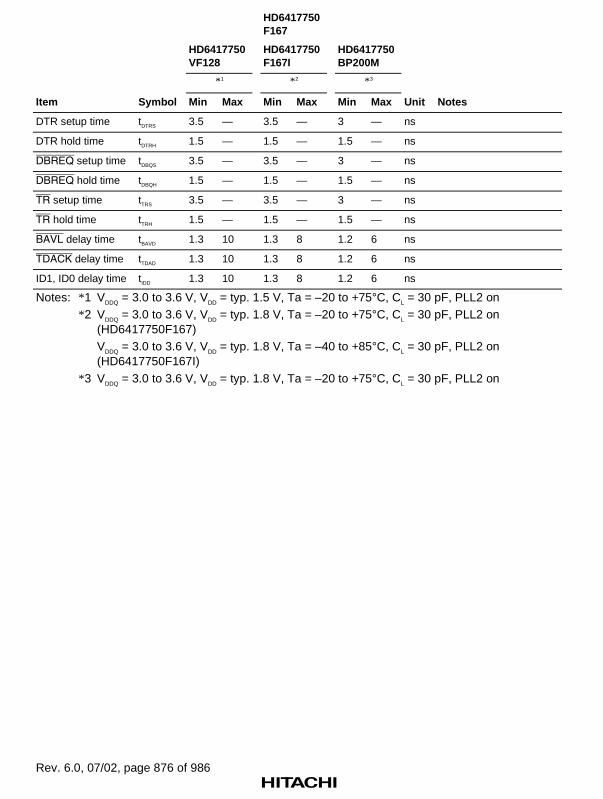
Rev. 6.0, 07/02, page 876 of 986
HD6417750VF128
HD6417750F167
HD6417750F167I
HD6417750BP200M
*1 *2 *3
Item Symbol Min Max Min Max Min Max Unit Notes
DTR setup time tDTRS 3.5 — 3.5 — 3 — ns
DTR hold time tDTRH 1.5 — 1.5 — 1.5 — ns
DBREQ setup time tDBQS 3.5 — 3.5 — 3 — ns
DBREQ hold time tDBQH 1.5 — 1.5 — 1.5 — ns
TR setup time tTRS 3.5 — 3.5 — 3 — ns
TR hold time tTRH 1.5 — 1.5 — 1.5 — ns
BAVL delay time tBAVD 1.3 10 1.3 8 1.2 6 ns
TDACK delay time tTDAD 1.3 10 1.3 8 1.2 6 ns
ID1, ID0 delay time tIDD 1.3 10 1.3 8 1.2 6 ns
Notes: *1 VDDQ = 3.0 to 3.6 V, VDD = typ. 1.5 V, Ta = –20 to +75°C, CL = 30 pF, PLL2 on*2 VDDQ = 3.0 to 3.6 V, VDD = typ. 1.8 V, Ta = –20 to +75°C, CL = 30 pF, PLL2 on
(HD6417750F167)VDDQ = 3.0 to 3.6 V, VDD = typ. 1.8 V, Ta = –40 to +85°C, CL = 30 pF, PLL2 on(HD6417750F167I)
*3 VDDQ = 3.0 to 3.6 V, VDD = typ. 1.8 V, Ta = –20 to +75°C, CL = 30 pF, PLL2 on

Rev. 6.0, 07/02, page 877 of 986
T1
tAD tAD
T2
CKIO
A25–A0
RD/
D63–D0(read)
D63–D0(write)
DACKn(DA)
tWDDtWDD tWDD
tRDHtRDS
tCSD tCSD
tRWD tRWD
tRSD tRSD tRSD
tWED1tWEDF tWEDF
tBSD tBSD
tDACD
tDACD
tDACDtDACD
tDACDFtDACDF
tDACD
Notes: IO: DACK deviceSA: Single address DMA transferDA: Dual address DMA transferDACK set to active-high
DACKn(SA: IO ← memory)
DACKn(SA: IO → memory)
Figure 22.15 SRAM Bus Cycle: Basic Bus Cycle (No Wait)

Rev. 6.0, 07/02, page 878 of 986
tWDDtWDD tWDD
tDACDFtDACDF
CKIO
A25–A0
RD/
D63–D0(read)
D63–D0(write)
DACKn(DA)
T1
tAD
Tw T2
tAD
tRDHtRDS
tCSD
tRWD tRWD
tCSD
tRSD tRSD tRSD
tWED1tWEDF tWEDF
tRDYHtRDYS
tBSD tBSD
tDACD
tDACD
tDACDtDACD
tDACD
DACKn(SA: IO ← memory)
DACKn(SA: IO → memory)
Notes: IO: DACK deviceSA: Single address DMA transferDA: Dual address DMA transferDACK set to active-high
Figure 22.16 SRAM Bus Cycle: Basic Bus Cycle (One Internal Wait)

Rev. 6.0, 07/02, page 879 of 986
tWDDtWDD tWDD
tDACDFtDACDF
CKIO
A25–A0
RD/
D63–D0(read)
D63–D0(write)
DACKn(DA)
T1
tAD
Tw Twe T2
tAD
tRDHtRDS
tCSD
tRWD tRWD
tCSD
tRSD tRSD tRSD
tWED1tWEDF tWEDF
tRDYHtRDYS
tRDYHtRDYS
tBSD tBSD
tDACD
tDACD
tDACDtDACD
tDACD
DACKn(SA: IO ← memory)
DACKn(SA: IO → memory)
Notes: IO: DACK deviceSA: Single address DMA transferDA: Dual address DMA transferDACK set to active-high
Figure 22.17 SRAM Bus Cycle: Basic Bus Cycle (One Internal Wait + One External Wait)

Rev. 6.0, 07/02, page 880 of 986
tWDDtWDD tWDD
tDACDFtDACDF
tDACD tDACDtDACD
TS1
tAD
T1 T2 TH1
tAD
tRDHtRDS
tCSD
tRWD tRWD
tCSD
tRSD tRSD tRSD
tWED1tWEDF tWEDF
tBSD tBSD
tDACD tDACD
CKIO
A25–A0
RD/
D63–D0(read)
D63–D0(write)
DACKn(SA: IO ← memory)
DACKn(SA: IO → memory)
DACKn(DA)
*
Notes: IO: DACK deviceSA: Single address DMA transferDA: Dual address DMA transferDACK set to active-high* SH7750R only
Figure 22.18 SRAM Bus Cycle: Basic Bus Cycle (No Wait, Address Setup/Hold TimeInsertion, AnS = 1, AnH = 1)

Rev. 6.0, 07/02, page 881 of 986
CKIO
A25–A5
T1 T2
RD/
D31–D0(read)
A4–A0
TB2 TB1 TB2 TB1 TB2 TB1
tCSD
tAD
tRWD
tBSD
tRDS
tBSD
tRSDtRSD
tRDH
tAD tAD
tCSD
tRWD
tRDH
tRSD
tRDS
DACKn(SA: IO ← memory)
DACKn(DA)
tDACD tDACD
tDACD tDACD
tDACD
Notes: IO: DACK deviceSA: Single address DMA transferDA: Dual address DMA transferDACK set to active-high
Figure 22.19 Burst ROM Bus Cycle (No Wait)

Rev. 6.0, 07/02, page 882 of 986
T1
T2
TB
2T
B1
TB
2T
B1
TB
2T
B1
Tw
bT
wb
Tw
bT
we
Tw
t AD
t CS
D
t RS
D
t RD
Ht R
DS
t BS
D
t AD
t RD
H
t RS
D
t RD
S
t AD
t CS
D t RD
YH
t RD
YS
t RD
YH
t RD
YS
t RD
YH
t RD
YS
t DA
CD
t DA
CD
t DA
CD
t DA
CD
t RW
Dt R
WD
CK
IO
A25
–A5
RD
/
D31
–D0
(rea
d)
A4–
A0
DA
CK
n(S
A: I
O ←
mem
ory)
DA
CK
n(D
A)
Not
es:
IO: D
AC
K d
evic
eS
A: S
ingl
e ad
dres
s D
MA
tran
sfer
DA
: Dua
l add
ress
DM
A tr
ansf
erD
AC
K s
et to
act
ive-
high
Figure 22.20 Burst ROM Bus Cycle(1st Data: One Internal Wait + One External Wait; 2nd/3rd/4th Data: One Internal Wait)

Rev. 6.0, 07/02, page 883 of 986
T1
TB
2
t CS
D
t RW
D
t BS
D
t RD
S
t BS
D
t RS
D
t AD
TS
1
t DA
CD
TB
1T
B2
t AD
t RD
H
t DA
CD
t DA
CD
TB
1T
B2
T2
TB
1
t AD
t CS
D
t RW
D
t RD
H
t RS
D
t RD
S
TH
1T
S1
TH
1T
S1
TH
1T
S1
TH
1
CK
IO
A25
–A5
RD
/
D31
–D0
(rea
d)
A4–
A0
DA
CK
n(S
A: I
O ←
mem
ory)
DA
CK
n(D
A)
Not
es:
IO: D
AC
K d
evic
eS
A: S
ingl
e ad
dres
s D
MA
tran
sfer
DA
: Dua
l add
ress
DM
A tr
ansf
erD
AC
K s
et to
act
ive-
high
t DA
CD
t DA
CD
Figure 22.21 Burst ROM Bus Cycle(No Wait, Address Setup/Hold Time Insertion, AnS = 1, AnH = 1)

Rev. 6.0, 07/02, page 884 of 986
Tw
T1
Tw
eT
B2
TB
1T
wb
Tw
beT
B1
TB
2T
wb
Tw
beT
wb
T2
TB
2T
wbe
TB
1
CK
IO
A25
–A5
A4–
A0
D31
–D0
(rea
d)
t AD
t AD
t AD t R
DH
t RD
St R
DH
t RD
S
DA
CK
n(D
A)
Not
es:
IO: D
AC
K d
evic
eS
A: S
ingl
e ad
dres
s D
MA
tran
sfer
DA
: Dua
l add
ress
DM
A tr
ansf
erD
AC
K s
et to
act
ive-
high
t DA
CD
t DA
CD
t DA
CD
t BS
Dt B
SD
t BS
Dt B
SD
t RS
Dt R
SD
t RW
D
t CS
D
t RW
D
t CS
D
t DA
CD
t DA
CD
t RS
D
RD
/
t RD
YH
t RD
YS
t RD
YH
t RD
YS
t RD
YH
t RD
YS
t RD
YH
t RD
YS
DA
CK
n(S
A: I
O ←
mem
ory)
Figure 22.22 Burst ROM Bus Cycle (One Internal Wait + One External Wait)

Rev. 6.0, 07/02, page 885 of 986
Trw
Tr
Tc1
Tc2
Tc3
Tc4
/Td1
Td2
Td4
Td3
Tpc
Tpc
Tpc
CK
IO
BA
NK
Pre
char
ge-s
el
D63
–D0
(rea
d)
Add
ress
Row
Row
Row
H/L
colu
mn
t AD
t AD
t AD
t RD
H
d0
t RD
S
DQ
Mn
D63
–D0
(writ
e)
CK
E
t WD
D
t WD
D
t CA
SD
2t C
AS
D2
t CA
SD
2
t DA
CD
t DA
CD
t DA
CD
t RA
SD
t RA
SD
t DQ
MD
t DQ
MD
t RW
D
t BS
Dt B
SD
RD
/
t CS
Dt C
SD
DA
CK
n(S
A: I
O ←
mem
ory)
Not
es:
IO: D
AC
K d
evic
eS
A: S
ingl
e ad
dres
s D
MA
tran
sfer
DA
: Dua
l add
ress
DM
A tr
ansf
erD
AC
K s
et to
act
ive-
high
t RW
D
Figure 22.23 Synchronous DRAM Auto-Precharge Read Bus Cycle: Single(RCD[1:0] = 01, CAS Latency = 3, TPC[2:0] = 011)

Rev. 6.0, 07/02, page 886 of 986
Trw
Tr
Tc1
Tc2
Tc3
Tc4
/Td1
Td2
Td4
Td3
Tpc
Tpc
Tpc
CK
IO
BA
NK
Pre
char
ge-s
el
D63
–D0
(rea
d)
Add
ress
t AD R
ow
Row
H/L c0
Row
t AD
t RD
Hd0
d1d2
d3
t RD
S
DQ
Mn
D63
–D0
(writ
e)
CK
E
t WD
D
t WD
D
t CA
SD
2t C
AS
D2
t CA
SD
2
t DA
CD
t DA
CD
t DA
CD
t RA
SD
t RA
SD
t DQ
MD
t DQ
MD
t RW
D
t BS
Dt B
SD
RD
/
t CS
Dt C
SD
t AD
DA
CK
n(S
A: I
O ←
mem
ory)
t RW
D
Not
es:
IO: D
AC
K d
evic
eS
A: S
ingl
e ad
dres
s D
MA
tran
sfer
DA
: Dua
l add
ress
DM
A tr
ansf
erD
AC
K s
et to
act
ive-
high
Figure 22.24 Synchronous DRAM Auto-Precharge Read Bus Cycle: Burst(RCD[1:0] = 01, CAS Latency = 3, TPC[2:0] = 011)
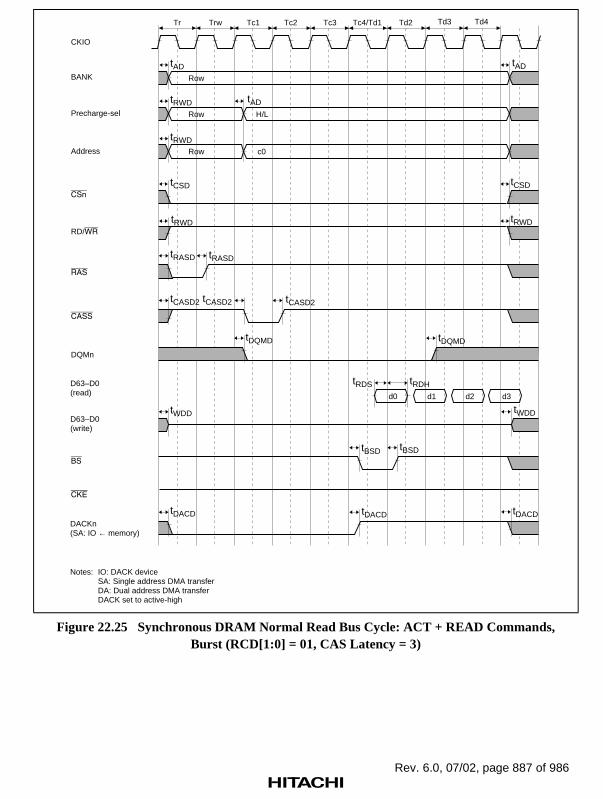
Rev. 6.0, 07/02, page 887 of 986
Tr Trw Tc1 Tc2 Tc3 Tc4/Td1 Td3Td2 Td4
CKIO
BANK
Precharge-sel
Address
RD/
DQMn
tAD
Row
Row H/L
Row c0
tAD
tRWD
tRWD tAD
tRDHtRDS
d0 d1 d2 d3
tCSD tCSD
tRWD tRWD
tRASD tRASD
tBSD tBSD
tDQMD tDQMD
tDACD tDACD
tWDD tWDD
tDACD
tCASD2 tCASD2tCASD2
D63–D0(read)
D63–D0(write)
DACKn(SA: IO ← memory)
Notes: IO: DACK deviceSA: Single address DMA transferDA: Dual address DMA transferDACK set to active-high
Figure 22.25 Synchronous DRAM Normal Read Bus Cycle: ACT + READ Commands,Burst (RCD[1:0] = 01, CAS Latency = 3)

Rev. 6.0, 07/02, page 888 of 986
Tpr Tpc Tr Trw Tc1 Tc2 Tc3 Tc4/Td1 Td3Td2 Td4
CKIO
BANK
Precharge-sel
Address
RD/
DQMn
tADRow
Row H/L
Row c0
tAD tAD
tAD
tRDHtRDSd0 d1 d2 d3
tCSDtCSD
tRWD tRWD
tRASD tRASD tRASDtRASD
tBSD tBSD
tDQMD
tDACD tDACD
tWDDtWDD
tDACD
tCASD2 tCASD2tCASD2
tDQMD
D63–D0(read)
D63–D0(write)
DACKn(SA: IO ← memory)
Notes: IO: DACK deviceSA: Single address DMA transferDA: Dual address DMA transferDACK set to active-high
Figure 22.26 Synchronous DRAM Normal Read Bus Cycle: PRE + ACT + READCommands, Burst (RCD[1:0] = 01, TPC[2:0] = 001, CAS Latency = 3)

Rev. 6.0, 07/02, page 889 of 986
Tc1 Tc2 Tc3 Tc4/Td1 Td3Td2 Td4
CKIO
BANK
Precharge-sel
Address
RD/
DQMn
tAD
Row
tAD
H/L
c0
tRDHtRDS
d0 d1 d2 d3
tCSD tCSD
tRWD tRWD
tRASD tRASD
tBSD tBSD
tDQMD tDQMD
tCASD2 tCASD2
tDACD tDACD
tWDD tWDD
tDACD
D63–D0(read)
D63–D0(write)
DACKn(SA: IO ← memory)
Notes: IO: DACK deviceSA: Single address DMA transferDA: Dual address DMA transferDACK set to active-high
Figure 22.27 Synchronous DRAM Normal Read Bus Cycle: READ Command, Burst(CAS Latency = 3)
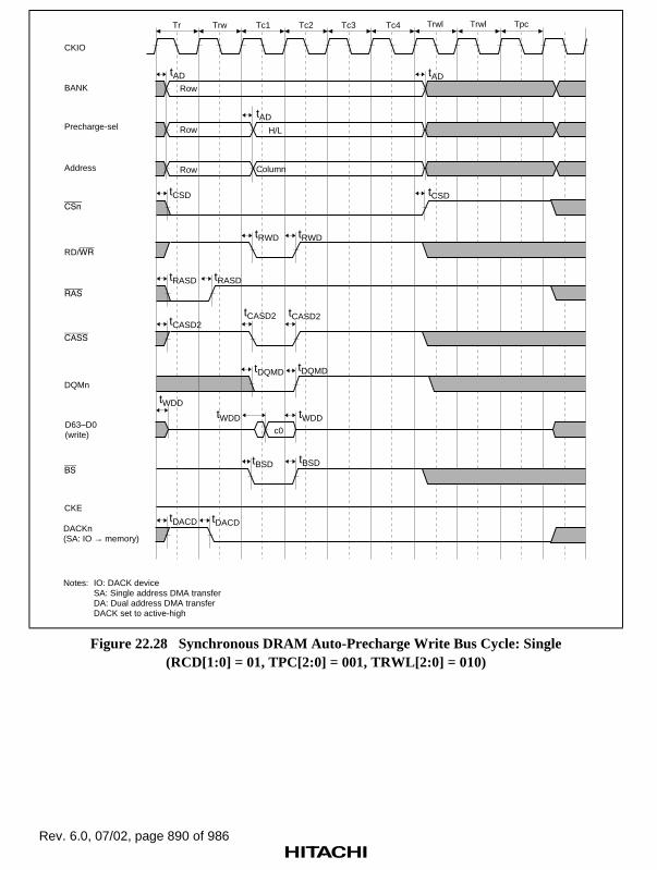
Rev. 6.0, 07/02, page 890 of 986
TrwTr Tc1 Tc2 Tc3 Tc4 Trwl Trwl Tpc
CKIO
BANK
Precharge-sel
Address
tAD tAD
tAD
H/L
Column Row
Row
Row
tWDD
c0
tWDD
DQMn
CKE
tWDD
tCASD2tCASD2tCASD2
tDACD tDACD
tRWD tRWD
tRASD tRASD
tDQMD tDQMD
tBSD tBSD
RD/
tCSD tCSD
D63–D0(write)
DACKn(SA: IO → memory)
Notes: IO: DACK deviceSA: Single address DMA transferDA: Dual address DMA transferDACK set to active-high
Figure 22.28 Synchronous DRAM Auto-Precharge Write Bus Cycle: Single(RCD[1:0] = 01, TPC[2:0] = 001, TRWL[2:0] = 010)

Rev. 6.0, 07/02, page 891 of 986
TrwTr Tc1 Tc2 Tc3 Tc4 Trwl Trwl Tpc
CKIO
BANK
Precharge-sel
Address
tAD tAD
tAD
H/L
c0Row
Row
Row
tWDD
d0
tWDD
d1 d2 d3
DQMn
CKE
tWDD
tCASD2
tCASD2tCASD2
tDACD tDACD
tRWD tRWD
tRASD tRASD
tDQMD tDQMD
tBSD tBSD
RD/
tCSD tCSD
D63–D0(write)
DACKn(SA: IO → memory)
Notes: IO: DACK deviceSA: Single address DMA transferDA: Dual address DMA transferDACK set to active-high
Figure 22.29 Synchronous DRAM Auto-Precharge Write Bus Cycle: Burst(RCD[1:0] = 01, TPC[2:0] = 001, TRWL[2:0] = 010)

Rev. 6.0, 07/02, page 892 of 986
TrwTr Tc1 Tc2 Tc3 Tc4 Trwl Trwl
CKIO
BANK
Precharge-sel
Address
tAD tAD
tAD
H/L
c0Row
Row
Row
tWDD
d0
tWDD
d1 d2 d3
DQMn
CKE
tWDD
tCASD2tCASD2tCASD2
tDACD tDACD
tRWD tRWD
tRASD tRASD
tDQMD tDQMD
tBSD tBSD
RD/
tCSD tCSD
D63–D0(write)
DACKn(SA: IO → memory)
Notes: IO: DACK deviceSA: Single address DMA transferDA: Dual address DMA transferDACK set to active-high
Figure 22.30 Synchronous DRAM Normal Write Bus Cycle: ACT + WRITE Commands,Burst (RCD[1:0] = 01, TRWL[2:0] = 010)

Rev. 6.0, 07/02, page 893 of 986
TrwTrTpcTpr Tc1 Tc2 Tc3 Tc4 Trwl Trwl
CKIO
BANK
Precharge-sel
Address
tAD tADtAD
H/L H/L
c0Row
Row
Row Row
tAD
tWDD
d0
tWDD
d1 d2 d3
DQMn
CKE
tWDD
tCASD2tCASD2tCASD2
tDQMD tDQMD
tDACD
tRWD tRWDtRWD tRWD
tRASD tRASD tRASD tRASD
tDACD tDACD
tBSD tBSD
RD/
tCSD tCSD
D63–D0(write)
DACKn(SA: IO → memory)
Notes: IO: DACK deviceSA: Single address DMA transferDA: Dual address DMA transferDACK set to active-high
Figure 22.31 Synchronous DRAM Normal Write Bus Cycle: PRE + ACT + WRITECommands, Burst (RCD[1:0] = 01, TPC[2:0] = 001, TRWL[2:0] = 010)

Rev. 6.0, 07/02, page 894 of 986
(Tnop)Tnop Tc1 Tc2 Tc3 Tc4 Trwl Trwl
tADtAD
H/L
c0
Row
tWDD
d0
tWDD
d1 d2 d3
tWDD
tDQMD tDQMD
tDACD
tRWD tRWD
tCASD2 tCASD2
tDACD
tBSD tBSD
tCSD tCSD
CKIO
BANK
Precharge-sel
Address
DQMn
CKE
RD/
D63–D0(write)
DACKn(SA: IO → memory)
Normal write
SA-DMA
Notes: In the case of SA-DMA only, the (Tnop) cycle is inserted, and the DACKn signal is output as shown by the solid line. In a normal write, the (Tnop) cycle is omitted and the DACKn signal is output as shown by the dotted line.IO: DACK deviceSA: Single address DMA transferDA: Dual address DMA transferDACK set to active-high
Figure 22.32 Synchronous DRAM Normal Write Bus Cycle: WRITE Command, Burst(TRWL[2:0] = 010)
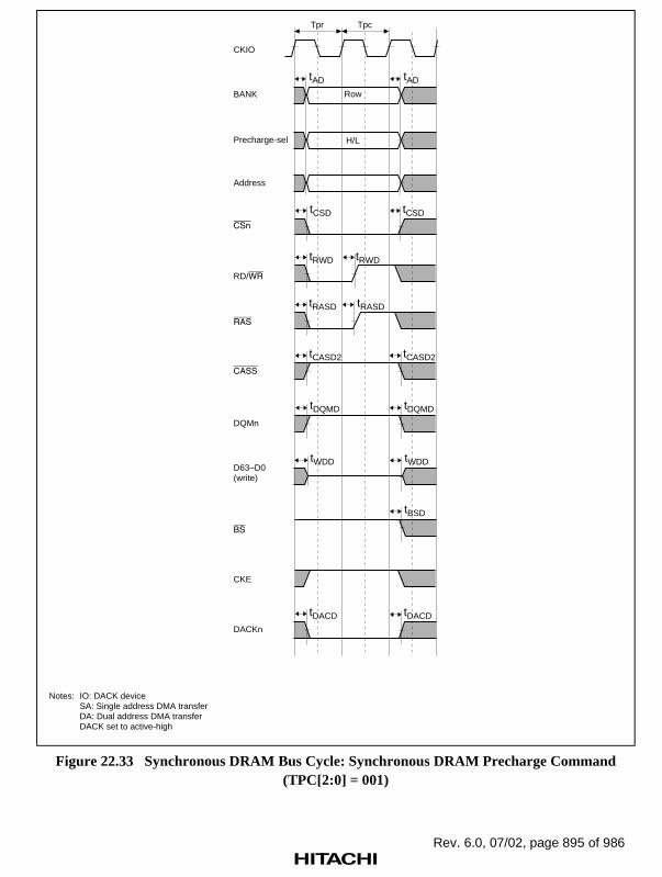
Rev. 6.0, 07/02, page 895 of 986
TpcTpr
CKIO
BANK
Precharge-sel
Address
tAD tAD
H/L
Row
DQMn
CKE
tCASD2 tCASD2
tDQMD tDQMD
tRWD tRWD
DACKn
tRASD tRASD
tDACD tDACD
tBSD
tWDDtWDD
RD/
tCSD tCSD
D63–D0(write)
Notes: IO: DACK deviceSA: Single address DMA transferDA: Dual address DMA transferDACK set to active-high
Figure 22.33 Synchronous DRAM Bus Cycle: Synchronous DRAM Precharge Command(TPC[2:0] = 001)
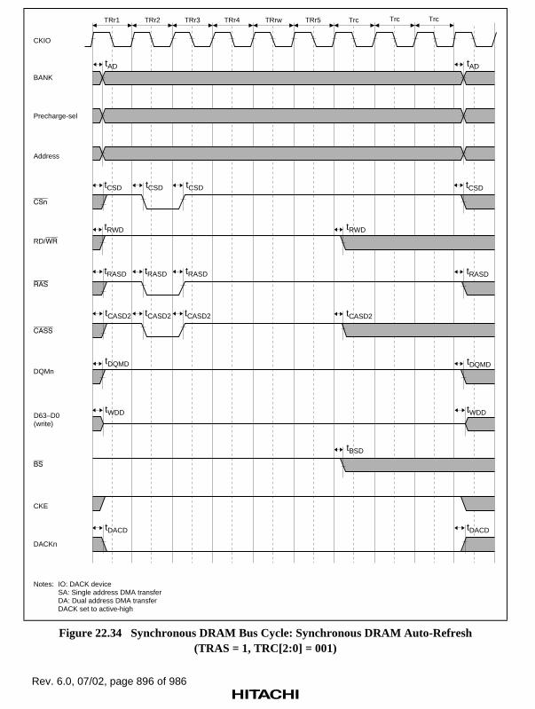
Rev. 6.0, 07/02, page 896 of 986
TRr1 TRr2 TRr3 TRr4 TRrw TRr5 TrcTrc Trc
CKIO
BANK
Precharge-sel
Address
RD/
DQMn
DACKn
Notes: IO: DACK deviceSA: Single address DMA transferDA: Dual address DMA transferDACK set to active-high
CKE
tAD tAD
tRWD tRWD
tDQMD tDQMD
tBSD
tDACD
tWDD tWDD
tCASD2 tCASD2tCASD2 tCASD2
tRASD tRASD tRASD tRASD
tCSD tCSD tCSD tCSD
tDACD
D63–D0(write)
Figure 22.34 Synchronous DRAM Bus Cycle: Synchronous DRAM Auto-Refresh(TRAS = 1, TRC[2:0] = 001)

Rev. 6.0, 07/02, page 897 of 986
CKIO
BANK
Precharge-sel
Address
RD/
DQMn
DACKn
Notes: IO: DACK deviceSA: Single address DMA transferDA: Dual address DMA transferDACK set to active-high
CKE
TRs1 TRs2 TRs3 TRs4 TRs5 TrcTrc Trc
tAD tAD
tRWD
tDQMD tDQMD
tDACD tDACD
tWDD tWDD
tCASD2 tCASD2
tCASD2
tCKED tCKED
tRASD
tRASDtRASD tRASD
tCSD
tCSDtCSD tCSD
D63–D0(write)
tRWD
tCASD2
tBSD
Figure 22.35 Synchronous DRAM Bus Cycle: Synchronous DRAM Self-Refresh(TRC[2:0] = 001)

Rev. 6.0, 07/02, page 898 of 986
TRp1 TRp2 TRp3 TRp4 TMw TMw2 TMw4TMw3 TMw5
CKIO
BANK
Precharge-sel
Address
RD/
DQMn
DACKn
Notes: IO: DACK deviceSA: Single address DMA transferDA: Dual address DMA transferDACK set to active-high
CKE
tAD tADtAD
tRWD tRWD tRWD
tCSD tCSD tCSD
tBSD
tDQMD
tDACD
tWDD tWDD
tDACD
tCASD2 tCASD2 tCASD2tCASD2
tRASD tRASD tRASD
tDQMD
D63–D0(write)
Figure 22.36 (a) Synchronous DRAM Bus Cycle: Synchronous DRAM Mode RegisterSetting (PALL)

Rev. 6.0, 07/02, page 899 of 986
TRp1 TRp2 TRp3 TRp4 TMw TMw2 TMw4TMw3 TMw5
CKIO
BANK
Precharge-sel
Address
RD/
DQMn
DACKn
Notes: IO: DACK deviceSA: Single address DMA transferDA: Dual address DMA transferDACK set to active-high
CKE
tAD tADtAD
tRWD tRWD tRWD
tCSDtCSD tCSD
tBSD
tDQMD
tDACD
tWDD tWDD
tDACD
tCASD2 tCASD2 tCASD2tCASD2
tRASD tRASD tRASD
tDQMD
D63–D0(write)
Figure 22.36 (b) Synchronous DRAM Bus Cycle: Synchronous DRAM Mode RegisterSetting (SET)

Rev. 6.0, 07/02, page 900 of 986
Tr2
Tr1
Trw
Tc1
Tcw
Tc2
Tpc
Tpc
t AD
t AD
t AD
Row
col
umn
t WD
Dt W
DD
t WD
Dt CA
SD
1t C
AS
D1
t CA
SD
1
t BS
Dt B
SD
t DA
CD
t DA
CD
t DA
CD
t CS
Dt C
SD
t DA
CD
t DA
CD
t DA
CD
t RW
Dt R
WD
t RA
SD
t RA
SD
t RA
SD
t RD
Ht R
DS
CK
IO
A25
–A0
RD
/
Tr2
Tr1
Tc1
Tc2
Tpc
t AD
t AD
t AD
Row
col
umn
t WD
Dt W
DD
t WD
Dt CA
SD
1t C
AS
D1
t CA
SD
1
t BS
Dt B
SD
t DA
CD
t DA
CD
t DA
CD
t CS
Dt C
SD
t DA
CD
t DA
CD
t DA
CD
t RW
Dt R
WD
t RA
SD
t RA
SD
t RA
SD
t RD
Ht R
DS
(1)
(2)
DA
CK
n(S
A: I
O ←
mem
ory)
DA
CK
n(S
A: I
O →
mem
ory)
D63
–D0
(rea
d)
D63
–D0
(writ
e)
Not
es:
IO: D
AC
K d
evic
eS
A: S
ingl
e ad
dres
s D
MA
tran
sfer
DA
: Dua
l add
ress
DM
A tr
ansf
erD
AC
K s
et to
act
ive-
high
Figure 22.37 DRAM Bus Cycles(1) RCD[1:0] = 00, AnW[2:0] = 000, TPC[2:0] = 001(2) RCD[1:0] = 01, AnW[2:0] = 001, TPC[2:0] = 010

Rev. 6.0, 07/02, page 901 of 986
Tr2T1r Tc1 Tc2 Tce Tpc
CKIO
tAD tAD tAD
Row Column
tWDD
tRASD tRASD tRASD
tRWD
tCASD1tCASD1tCASD1
tBSD tBSD
RD/
tCSD tCSD
tDACD tDACD
tRDHtRDS
A25–A0
DACKn(SA: IO ← memory)
D63–D0(read)
D63–D0(write)
tRWD
Notes: IO: DACK deviceSA: Single address DMA transferDA: Dual address DMA transferDACK set to active-high
Figure 22.38 DRAM Bus Cycle(EDO Mode, RCD[1:0] = 00, AnW[2:0] = 000, TPC[2:0] = 001)
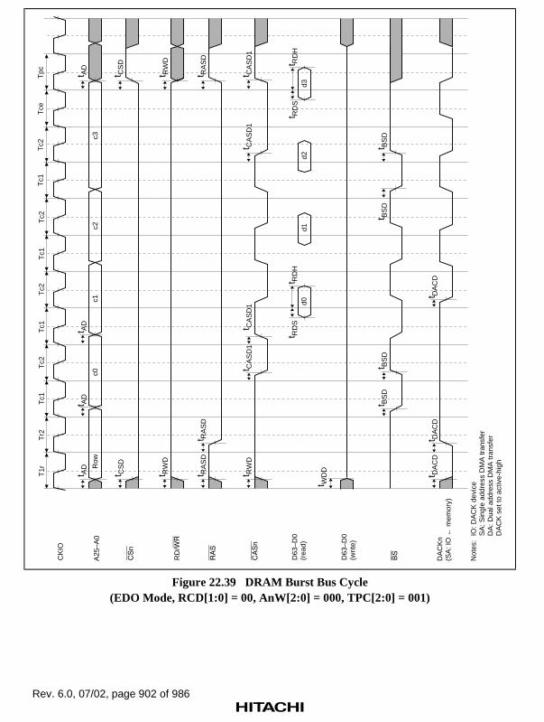
Rev. 6.0, 07/02, page 902 of 986
Tr2
T1r
Tc1
Tc2
Tc1
Tc2
Tc1
Tc1
Tc2
Tc2
Tce
Tpc
t AD
t AD
t AD
t AD
Row
c0c1
c2c3
t WD
Dt RA
SD
t RA
SD
t RA
SD
t RW
D
t RW
D
t CA
SD
1t C
AS
D1
t CA
SD
1t C
AS
D1
t BS
Dt B
SD
t BS
Dt B
SD
t DA
CD
t CS
Dt C
SD
t DA
CD
t DA
CD
t RW
D
t RD
Ht R
DS
d0
t RD
Ht R
DS
d3d2
d1
CK
IO
RD
/
A25
–A0
DA
CK
n(S
A: I
O ←
mem
ory)
Not
es:
IO: D
AC
K d
evic
eS
A: S
ingl
e ad
dres
s D
MA
tran
sfer
DA
: Dua
l add
ress
DM
A tr
ansf
erD
AC
K s
et to
act
ive-
high
D63
–D0
(rea
d)
D63
–D0
(writ
e)
Figure 22.39 DRAM Burst Bus Cycle(EDO Mode, RCD[1:0] = 00, AnW[2:0] = 000, TPC[2:0] = 001)

Rev. 6.0, 07/02, page 903 of 986
Tr2
Tr1
Trw
Tc1
Tcw
Tc2
Tc1
Tc2
Tcw
Tc1
Tcw
Tc1
Tc2
Tce
Tpc
Tcw
Tc2
CK
IO
t AD
t AD
t AD
t RD
Hd0
t RD
St R
DH
d3d2
d1
t RD
S
t RA
SD
t RA
SD
Row
c0c1
c2c3
RD
/
t CS
Dt C
SD
t CA
SD
1t C
AS
D1
t CA
SD
1t C
AS
D1
t RA
SD
t CA
SD
1t C
AS
D1
t BS
Dt B
SD
t DA
CD
t DA
CD
t DA
CD
t RW
Dt R
WD
t WD
D
A25
–A0
DA
CK
n(S
A: I
O ←
mem
ory)
Not
es:
IO: D
AC
K d
evic
eS
A: S
ingl
e ad
dres
s D
MA
tran
sfer
DA
: Dua
l add
ress
DM
A tr
ansf
erD
AC
K s
et to
act
ive-
high
D63
–D0
(rea
d)
D63
–D0
(writ
e)
Figure 22.40 DRAM Burst Bus Cycle(EDO Mode, RCD[1:0] = 01, AnW[2:0] = 001, TPC[2:0] = 001)

Rev. 6.0, 07/02, page 904 of 986
Tr2
Tr1
Trw
Tc1
Tcw
Tc2
Tcn
wT
cwT
c1T
c2T
c2T
cwT
cnw
Tc1
Tcw
Tcn
wT
c1T
c2T
cnw
Tce
Tpc
CK
IO
t AD
t AD
t AD
t RD
Hd0
t RD
St R
DH
d3d2
d1t R
DS
t RA
SD
t RA
SD
Row
c0c1
c2c3
RD
/
t CS
Dt C
SD
t CA
SD
1t C
AS
D1
t CA
SD
1
t RA
SD
t CA
SD
1t C
AS
D1
t BS
Dt B
SD
t DA
CD
t DA
CD
t DA
CD
t RW
Dt R
WD
t WD
D
A25
–A0
DA
CK
n(S
A: I
O ←
mem
ory)
Not
es:
IO: D
AC
K d
evic
eS
A: S
ingl
e ad
dres
s D
MA
tran
sfer
DA
: Dua
l add
ress
DM
A tr
ansf
erD
AC
K s
et to
act
ive-
high
D63
–D0
(rea
d)
D63
–D0
(writ
e)
Figure 22.41 DRAM Burst Bus Cycle (EDO Mode, RCD[1:0] = 01, AnW[2:0] = 001,TPC[2:0] = 001, 2-Cycle CAS Negate Pulse Width)

Rev. 6.0, 07/02, page 905 of 986
Tr1
t AD
Row
Tc1
Tc2
Tc1
Tc2
Tr2
Tpc
c0c1
c2c3
CK
IO
RD
/
t AD
t AD
t AD
t RD
Ht R
DS
t RD
Ht R
DS
t CS
D
t RW
Dt R
WD
t CS
D t CA
SD
1
t RA
SD
t WD
D
t RA
SD
t CA
SD
1t C
AS
D1
t CA
SD
1t C
AS
D1
d3d2
d1d0
t BS
Dt B
SD
t BS
Dt B
SD
t DA
CD
t DA
CD
t DA
CD
Tc1
Tc1
Tc2
Tce
Tc2
A25
–A0
DA
CK
n(S
A: I
O ←
mem
ory)
Not
es:
IO: D
AC
K d
evic
eS
A: S
ingl
e ad
dres
s D
MA
tran
sfer
DA
: Dua
l add
ress
DM
A tr
ansf
erD
AC
K s
et to
act
ive-
high
D63
–D0
(rea
d)
D63
–D0
(writ
e)
Figure 22.42 DRAM Burst Bus Cycle: RAS Down Mode State(EDO Mode, RCD[1:0] = 00, AnW[2:0] = 000)

Rev. 6.0, 07/02, page 906 of 986
Tr1
Tc1
Tc2
Tc1
Tc2
Tr2
c0c1
c2c3
CK
IO
A25
–A0
RD
/
t AD
t AD
t AD
t RD
Ht R
DS
t RD
Ht R
DS
t CS
D
t RW
Dt R
WD
t RA
SD
RA
S-d
own
mod
e en
ded
t CS
D t CA
SD
1
t WD
D
t CA
SD
1t C
AS
D1
t CA
SD
1t C
AS
D1
d3d2
d1d0
t BS
Dt B
SD
t BS
Dt B
SD
t DA
CD
t DA
CD
Tc1
Tce
Tc2
DA
CK
n(S
A: I
O ←
mem
ory)
Not
es:
IO: D
AC
K d
evic
eS
A: S
ingl
e ad
dres
s D
MA
tran
sfer
DA
: Dua
l add
ress
DM
A tr
ansf
erD
AC
K s
et to
act
ive-
high
D63
–D0
(rea
d)
D63
–D0
(writ
e)
Figure 22.43 DRAM Burst Bus Cycle: RAS Down Mode Continuation(EDO Mode, RCD[1:0] = 00, AnW[2:0] = 000)

Rev. 6.0, 07/02, page 907 of 986
Tr1
Tr2
Tc1
Tc2
Tc1
Tc2
Tc2
Tc1
Tc1
Tc2
Tpc
CK
IO
A25
–A0
RD
/
D63
–D0
(rea
d)
D63
–D0
(writ
e)
DA
CK
n(S
A: I
O →
mem
ory)
Not
es:
IO: D
AC
K d
evic
eS
A: S
ingl
e ad
dres
s D
MA
tran
sfer
DA
: Dua
l add
ress
DM
A tr
ansf
erD
AC
K s
et to
act
ive-
high
DA
CK
n(S
A: I
O ←
mem
ory)
t AD
c0R
owc1
c2c3
t AD
t AD
t RW
Dt R
WD
t RD
Ht R
DS
d0
t WD
D
d0d1
d2d3
t BS
Dt B
SD
t WD
D
d1d2
t RD
H
t WD
D
t RD
S
d3t W
DD
t CS
Dt C
SD
t DA
CD
t DA
CD
t DA
CD
t CA
SD
1t C
AS
D1
t CA
SD
1t C
AS
D1
t CA
SD
1
t RA
SD
t RA
SD
t RA
SD
t DA
CD
t DA
CD
t DA
CD
Figure 22.44 DRAM Burst Bus Cycle(Fast Page Mode, RCD[1:0] = 00, AnW[2:0] = 000, TPC[2:0] = 001)

Rev. 6.0, 07/02, page 908 of 986
Tr1
Tr2
Trw
Tc1
Tcw
Tc2
Tcw
Tc1
Tc2
Tc1
Tcw
CK
IO
RD
/
t AD
c0R
owc1
c2c3
t AD
t AD
t RW
Dt R
WD
t RD
Ht R
DS
d0
t WD
D
d0d1
d2d3
t BS
Dt B
SD
t WD
D
d1d2
t RD
H
t WD
D
t RD
Sd3
t WD
D
t CS
Dt C
SD
t DA
CD
t DA
CD
t DA
CD
t CA
SD
1t C
AS
D1
t CA
SD
1t C
AS
D1
t CA
SD
1
t RA
SD
t RA
SD
t RA
SD
t DA
CD
t DA
CD
t DA
CD
Tc1
Tc2
Tc2
Tcw
Tpc
A25
–A0
D63
–D0
(rea
d)
D63
–D0
(writ
e)
DA
CK
n(S
A: I
O →
mem
ory)
Not
es:
IO: D
AC
K d
evic
eS
A: S
ingl
e ad
dres
s D
MA
tran
sfer
DA
: Dua
l add
ress
DM
A tr
ansf
erD
AC
K s
et to
act
ive-
high
DA
CK
n(S
A: I
O ←
mem
ory)
Figure 22.45 DRAM Burst Bus Cycle(Fast Page Mode, RCD[1:0] = 01, AnW[2:0] = 001, TPC[2:0] = 001)

Rev. 6.0, 07/02, page 909 of 986
Tr1
Tr2
Trw
Tc1
Tcw
Tc2
Tc1
Tcn
wT
cwT
c2T
cnw
CK
IO
RD
/
t AD
c0R
owc1
c2c3
t AD
t AD
t RW
Dt R
WD
t RD
Ht R
DS
d0
t WD
Dd0
d1d2
d3
t BS
Dt B
SD
t WD
D
d1d2
t RD
H
t WD
D
t RD
Sd3
t WD
D
t CS
Dt C
SD
t DA
CD
t DA
CD
t DA
CD
t CA
SD
1t C
AS
D1
t CA
SD
1t C
AS
D1
t CA
SD
1
t RA
SD
t RA
SD
t RA
SD
t DA
CD
t DA
CD
t DA
CD
Tcw
Tc1
Tcn
wT
c2T
c1T
pcT
c2T
cnw
Tcw
A25
–A0
D63
–D0
(rea
d)
D63
–D0
(writ
e)
DA
CK
n(S
A: I
O →
mem
ory)
Not
es:
IO: D
AC
K d
evic
eS
A: S
ingl
e ad
dres
s D
MA
tran
sfer
DA
: Dua
l add
ress
DM
A tr
ansf
erD
AC
K s
et to
act
ive-
high
DA
CK
n(S
A: I
O ←
mem
ory)
Figure 22.46 DRAM Burst Bus Cycle (Fast Page Mode, RCD[1:0] = 01, AnW[2:0] = 001,TPC[2:0] = 001, 2-Cycle CAS Negate Pulse Width)

Rev. 6.0, 07/02, page 910 of 986
Tpc
Tr1
Tr2
Tc1
Tc2
Tc1
Tc1
Tc2
Tc2
Tc1
Tc2
CK
IO
A25
–A0
RD
/
D63
–D0
(rea
d)
D63
–D0
(writ
e)
DA
CK
n(S
A: I
O →
mem
ory)
Not
es:
IO: D
AC
K d
evic
eS
A: S
ingl
e ad
dres
s D
MA
tran
sfer
DA
: Dua
l add
ress
DM
A tr
ansf
erD
AC
K s
et to
act
ive-
high
DA
CK
n(S
A: I
O ←
mem
ory)
t AD
c0R
owc1
c2c3
t AD
t AD
t AD
t RW
Dt R
WD
t RW
D
t RD
Ht R
DS
d0
t WD
D
d0d1
d2d3
t BS
Dt B
SD
t WD
D
d1d2
t RD
H
t WD
D
t RD
Sd3
t WD
D
t CS
Dt C
SD
t CS
D
t DA
CD
t DA
CD
t DA
CD
t CA
SD
1t C
AS
D1
t CA
SD
1t C
AS
D1
t CA
SD
1
t DA
CD
t DA
CD
t DA
CD
t RA
SD
t RA
SD
Figure 22.47 DRAM Burst Bus Cycle: RAS Down Mode State(Fast Page Mode, RCD[1:0] = 00, AnW[2:0] = 000)

Rev. 6.0, 07/02, page 911 of 986
CK
IO
RD
/
t AD
c0c1
c2c3
t AD
t RW
Dt R
WD
t RW
D
t RD
Ht R
DS
d0
t WD
D
d0d1
d2d3
t BS
Dt B
SD
t WD
D
d1d2
t RD
H
t WD
D
t RD
Sd3
t WD
D
t CS
Dt C
SD
t CS
D
t RA
SD
RA
S d
own
mod
e en
ded
t DA
CD
t DA
CD
t DA
CD
t CA
SD
1t C
AS
D1
t CA
SD
1t C
AS
D1
t CA
SD
1
t DA
CD
t DA
CD
t DA
CD
Tno
pT
c1T
c2T
c1T
c1T
c2T
c2T
c1T
c2
A25
–A0
D63
–D0
(rea
d)
D63
–D0
(writ
e)
DA
CK
n(S
A: I
O →
mem
ory)
Not
es:
IO: D
AC
K d
evic
eS
A: S
ingl
e ad
dres
s D
MA
tran
sfer
DA
: Dua
l add
ress
DM
A tr
ansf
erD
AC
K s
et to
act
ive-
high
DA
CK
n(S
A: I
O ←
mem
ory)
Figure 22.48 DRAM Burst Bus Cycle: RAS Down Mode Continuation(Fast Page Mode, RCD[1:0] = 00, AnW[2:0] = 000)

Rev. 6.0, 07/02, page 912 of 986
TRr1 TRr2 TRr3 TRr4 TRr5 Trc TrcTrc
CKIO
A25–A0
RD/
D63–D0(write)
DACKn(SA: IO → memory)
Notes: IO: DACK deviceSA: Single address DMA transferDA: Dual address DMA transferDACK set to active-high
DACKn(SA: IO ← memory)
tAD
tWDD
tDACD
tDACD
tCSD
tRWD
tRASDtRASD tRASD
tCASD1
tCASD1 tCASD1
Figure 22.49 DRAM Bus Cycle: DRAM CAS-Before-RAS Refresh(TRAS[2:0] = 000, TRC[2:0] = 001)
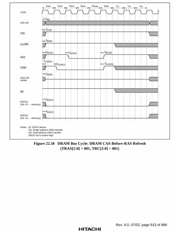
Rev. 6.0, 07/02, page 913 of 986
TRr1 TRr2 TRr3 TRr4 TRr5TRr4w Trc Trc Trc
CKIO
RD/
tAD
tWDD
tDACD
tDACD
tCSD
tRWD
tRASDtRASD tRASD
tCASD1
tCASD1tCASD1
A25–A0
D63–D0(write)
DACKn(SA: IO → memory)
Notes: IO: DACK deviceSA: Single address DMA transferDA: Dual address DMA transferDACK set to active-high
DACKn(SA: IO ← memory)
Figure 22.50 DRAM Bus Cycle: DRAM CAS-Before-RAS Refresh(TRAS[2:0] = 001, TRC[2:0] = 001)

Rev. 6.0, 07/02, page 914 of 986
TRr1 TRr2 TRr3 TRr4 TRr5 Trc TrcTrc
CKIO
RD/
tAD
tWDD
tDACD
tDACD
tCSD
tRWD
tRASDtRASD tRASD
tCASD1
tCASD1 tCASD1
A25–A0
D63–D0(write)
DACKn(SA: IO → memory)
Notes: IO: DACK deviceSA: Single address DMA transferDA: Dual address DMA transferDACK set to active-high
DACKn(SA: IO ← memory)
Figure 22.51 DRAM Bus Cycle: DRAM Self-Refresh (TRC[2:0] = 001)

Rev. 6.0, 07/02, page 915 of 986
Tpc
m1
Tpc
m2
Tpc
m0
Tpc
m1
Tpc
m2
Tpc
m1w
Tpc
m1w
Tpc
m2w
CK
IO
()
RD
/
D15
–D0
(rea
d)
D15
–D0
(writ
e)
DA
CK
n(D
A)
t AD
t AD
t WD
D
t BS
Dt B
SD
t BS
Dt B
SD
t WD
Dt W
DD
t RW
D
t CS
Dt C
SD
t RW
D
t RS
Dt R
SD
t RS
D
t WE
DF
t WE
D1
t WE
DF
t DA
CD
t RD
Ht R
DS
t RD
YH
t RD
YS
t RD
YH
t RD
YS
t DA
CD
t AD
t AD
t WD
D
t WD
Dt W
DD
t RW
D
t CS
Dt C
SD
t RW
D
t RS
Dt R
SD
t RS
D
t WE
DF
t WE
D1
t WE
DF
t DA
CD
TE
DT
EHt R
DH
t RD
S
t DA
CD
(1)
(2)
A25
–A0
Not
es:
IO: D
AC
K d
evic
eS
A: S
ingl
e ad
dres
s D
MA
tran
sfer
DA
: Dua
l add
ress
DM
A tr
ansf
erD
AC
K s
et to
act
ive-
high
*: S
H77
50S
onl
y
*
Figure 22.52 PCMCIA Memory Bus Cycle(1) TED[2:0] = 000, TEH[2:0] = 000, No Wait
(2) TED[2:0] = 001, TEH[2:0] = 001, One Internal Wait + One External Wait

Rev. 6.0, 07/02, page 916 of 986
Tpc
i1T
pci2
Tpc
i0T
pci1
Tpc
i2T
pci1
wT
pci1
wT
pci2
w
CK
IO
()
RD
/
()
DA
CK
n(D
A)
Not
es:
IO: D
AC
K d
evic
eS
A: S
ingl
e ad
dres
s D
MA
tran
sfer
DA
: Dua
l add
ress
DM
A tr
ansf
erD
AC
K s
et to
act
ive-
high
()
t AD
t AD
t BS
Dt B
SD
t BS
Dt B
SD
t WD
Dt W
DD
t RW
D
t CS
Dt C
SD
t RW
D t ICR
SD
t ICR
SD
t ICW
SD
Ft IC
WS
DF
t DA
CD
t RD
Ht R
DS
t RD
YH
t RD
YS
t RD
YH
t RD
YS
t IO16
Ht IO
16S
t IO16
Ht IO
16S
t DA
CD
t AD
t AD
t WD
D
t WD
Dt W
DD
t RW
D
t CS
Dt C
SD
t RW
D
t ICR
SD
t ICR
SD
t ICR
SD
t ICW
SD
F
t ICW
SD
Ft IC
WS
DF
t DA
CD
t RD
Ht R
DS
t DA
CD
D15
–D0
(rea
d)
D15
–D0
(writ
e)
(1)
(2)
A25
–A0
Figure 22.53 PCMCIA I/O Bus Cycle(1) TED[2:0] = 000, TEH[2:0] = 000, No Wait
(2) TED[2:0] = 001, TEH[2:0] = 001, One Internal Wait + One External Wait

Rev. 6.0, 07/02, page 917 of 986
Tpc
i0T
pci1
Tpc
i2w
Tpc
i2T
pci1
wT
pci0
Tpc
i1T
pci2
wT
pci2
Tpc
i1w
CK
IO
A25
–A1
A0
()
RD
/
()
D15
–D0
(rea
d)
D15
–D0
(writ
e)
Not
es:
IO: D
AC
K d
evic
eS
A: S
ingl
e ad
dres
s D
MA
tran
sfer
DA
: Dua
l add
ress
DM
A tr
ansf
erD
AC
K s
et to
act
ive-
high
()
t BS
Dt B
SD
t AD
t AD
t WD
D
t WD
Dt W
DD
t WD
Dt W
DD
t RW
Dt R
WD
t AD
t CS
Dt C
SD
t CS
D
t ICR
SD
t ICR
SD
t ICR
SD
t ICW
SD
Ft IC
WS
DF
t ICW
SD
Ft IC
WS
DF
t ICW
SD
F
t RD
Ht R
DS
t RD
YS
t RD
YH
t IO16
St IO
16H
t RD
YS
t RD
YH
Figure 22.54 PCMCIA I/O Bus Cycle(TED[2:0] = 001, TEH[2:0] = 001, One Internal Wait, Bus Sizing)

Rev. 6.0, 07/02, page 918 of 986
Tm
1T
md1
wT
md1
Tm
0T
md1
wT
md1
Tm
d1w
CK
IO
RD
/
D63
–D0
DA
CK
n(D
A)/
t FM
Dt F
MD
t BS
Dt B
SD
t BS
Dt B
SD
t CS
Dt C
SD
t DA
CD
t RD
H
t RD
S D0
t RD
YH
t RD
YS
t DA
CD
t RW
Dt R
WD
t WE
D1
t WE
D1
t FM
Dt F
MD
t CS
Dt C
SDt R
DH
t RD
St W
DD
AD
0
t WD
Dt W
DD
A
t WD
D
t RW
Dt R
WD
t WE
D1
t WE
D1
t DA
CD
t DA
CD
t RD
YH
t RD
YS
t RD
YH
t RD
YS
1st d
ata
bus
cycl
e in
form
atio
nD
63–D
61: A
cces
s si
ze00
0: B
yte
001:
Wor
d (2
byt
es)
010:
Lon
g (4
byt
es)
011:
Qua
d (8
byt
es)
1xx:
Bur
st (
32 b
ytes
)D
25–D
0: A
ddre
ss
1st d
ata
bus
cycl
e in
form
atio
nD
63–D
61: A
cces
s si
ze00
0: B
yte
001:
Wor
d (2
byt
es)
010:
Lon
g (4
byt
es)
011:
Qua
d (8
byt
es)
1xx:
Bur
st (
32 b
ytes
)D
25–D
0: A
ddre
ss
Not
es:
IO: D
AC
K d
evic
eS
A: S
ingl
e ad
dres
s D
MA
tran
sfer
DA
: Dua
l add
ress
DM
A tr
ansf
erD
AC
K s
et to
act
ive-
high
(1)
(2)
Figure 22.55 MPX Basic Bus Cycle: Read(1) 1st Data (One Internal Wait)
(2) 1st Data (One Internal Wait + One External Wait)

Rev. 6.0, 07/02, page 919 of 986
Tm
1T
md1
wT
md1
CK
IO
RD
/
D63
–D0
DA
CK
n(D
A)
Not
es:
IO: D
AC
K d
evic
eS
A: S
ingl
e ad
dres
s D
MA
tran
sfer
DA
: Dua
l add
ress
DM
A tr
ansf
erD
AC
K s
et to
act
ive-
high
/
t FM
Dt F
MD
t BS
Dt B
SD
t CS
Dt C
SD
t DA
CD
t RD
YH
t RD
YS
t DA
CD
t WE
D1
t WE
D1
Tm
1T
md1
t FM
Dt F
MD
t BS
Dt B
SD
t CS
Dt C
SD
t DA
CD
D0
D0
t RD
YH
t RD
YS
t DA
CD
t RW
Dt R
WD
t RW
Dt R
WD
t WE
D1
t WE
D1
A
t RD
YH
t RD
YS
t RD
YH
t RD
YS
t WD
Dt W
DD
t WD
DA
t WD
Dt W
DD
t WD
D
Tm
1T
md1
wT
md1
wT
md1
t FM
Dt F
MD
t BS
Dt B
SD
t CS
Dt C
SD
t DA
CD
t DA
CD
t WE
D1
t WE
D1
D0
t RW
Dt R
WD
A
t WD
Dt W
DD
t WD
D
1st d
ata
bus
cycl
e in
form
atio
nD
63–D
61: A
cces
s si
ze00
0: B
yte
001:
Wor
d (2
byt
es)
010:
Lon
g (4
byt
es)
011:
Qua
d (8
byt
es)
1xx:
Bur
st (
32 b
ytes
)D
25–D
0: A
ddre
ss
1st d
ata
bus
cycl
e in
form
atio
nD
63–D
61: A
cces
s si
ze00
0: B
yte
001:
Wor
d (2
byt
es)
010:
Lon
g (4
byt
es)
011:
Qua
d (8
byt
es)
1xx:
Bur
st (
32 b
ytes
)D
25–D
0: A
ddre
ss
1st d
ata
bus
cycl
e in
form
atio
nD
63–D
61: A
cces
s si
ze00
0: B
yte
001:
Wor
d (2
byt
es)
010:
Lon
g (4
byt
es)
011:
Qua
d (8
byt
es)
1xx:
Bur
st (
32 b
ytes
)D
25–D
0: A
ddre
ss
(1)
(2)
(3)
Figure 22.56 MPX Basic Bus Cycle: Write(1) 1st Data (No Wait)
(2) 1st Data (One Internal Wait)(3) 1st Data (One Internal Wait + One External Wait)

Rev. 6.0, 07/02, page 920 of 986
CK
IO
RD
/
D63
–D0
DA
CK
n(D
A)
Not
es:
IO: D
AC
K d
evic
eS
A: S
ingl
e ad
dres
s D
MA
tran
sfer
DA
: Dua
l add
ress
DM
A tr
ansf
erD
AC
K s
et to
act
ive-
high
/
Tm
1T
md1
wT
md1
Tm
d2T
md3
Tm
d4
t FM
Dt F
MD
t BS
Dt B
SD
t CS
Dt C
SD
t RD
YS
t RD
YH
t DA
CD
t DA
CD
t WE
D1
t WE
D1
D3
t RW
Dt R
WD
A
t WD
DD
2D
1D
0
t WD
Dt R
DH
t RD
S
Tm
1T
md1
wT
md1
Tm
d2w
Tm
d2T
md3
Tm
d4w
Tm
d4
t FM
Dt F
MD
t BS
Dt B
SD
t CS
Dt C
SD
t RD
YS
t RD
YH
t RD
YH
t RD
YS
t DA
CD
t DA
CD
t WE
D1
t WE
D1
D3
t RW
Dt R
WD
A
t WD
DD
2D
1D
0
t WD
Dt R
DH
t RD
S
1st d
ata
bus
cycl
e in
form
atio
nD
63–D
61: A
cces
s si
ze00
0: B
yte
001:
Wor
d (2
byt
es)
010:
Lon
g (4
byt
es)
011:
Qua
d (8
byt
es)
1xx:
Bur
st (
32 b
ytes
)D
25–D
0: A
ddre
ss
1st d
ata
bus
cycl
e in
form
atio
nD
63–D
61: A
cces
s si
ze00
0: B
yte
001:
Wor
d (2
byt
es)
010:
Lon
g (4
byt
es)
011:
Qua
d (8
byt
es)
1xx:
Bur
st (
32 b
ytes
)D
25–D
0: A
ddre
ss
(1)
(2)
Figure 22.57 MPX Bus Cycle: Burst Read(1) 1st Data (One Internal Wait), 2nd to 8th Data (One Internal Wait)
(2) 1st Data (One Internal Wait), 2nd to 4th Data (One Internal Wait + One External Wait)

Rev. 6.0, 07/02, page 921 of 986
CK
IO
RD
/
D63
–D0
DA
CK
n(D
A)
Not
es:
IO: D
AC
K d
evic
eS
A: S
ingl
e ad
dres
s D
MA
tran
sfer
DA
: Dua
l add
ress
DM
A tr
ansf
erD
AC
K s
et to
act
ive-
high
/
Tm
1T
md1
Tm
d2T
md3
Tm
d4
t FM
Dt F
MD
t BS
Dt B
SD
t CS
Dt C
SD
t RD
YS
t RD
YH
t DA
CD
t DA
CD
t WE
D1
t WE
D1
D3
t RW
Dt R
WD
A
t WD
D
D2
D1
D0
D3
D2
D1
D0
t WD
D
Tm
1T
md1
wT
md1
Tm
d2w
Tm
d2T
md3
Tm
d4w
Tm
d4
t FM
Dt F
MD
t BS
Dt B
SD
t CS
Dt C
SD
t RD
YS
t RD
YH
t RD
YH
t RD
YS
t DA
CD
t DA
CD
t WE
D1
t WE
D1
t RW
Dt R
WD
A
t WD
Dt W
DD
1st d
ata
bus
cycl
e in
form
atio
nD
63–D
61: A
cces
s si
ze00
0: B
yte
001:
Wor
d (2
byt
es)
010:
Lon
g (4
byt
es)
011:
Qua
d (8
byt
es)
1xx:
Bur
st (
32 b
ytes
)D
25–D
0: A
ddre
ss
1st d
ata
bus
cycl
e in
form
atio
nD
63–D
61: A
cces
s si
ze00
0: B
yte
001:
Wor
d (2
byt
es)
010:
Lon
g (4
byt
es)
011:
Qua
d (8
byt
es)
1xx:
Bur
st (
32 b
ytes
)D
25–D
0: A
ddre
ss
(1)
(2)
Figure 22.58 MPX Bus Cycle: Burst Write(1) No Internal Wait
(2) 1st Data (One Internal Wait), 2nd to 4th Data (No Internal Wait + External WaitControl)

Rev. 6.0, 07/02, page 922 of 986
T1
Tw
T2
CK
IO
RD
/
(1)
D63
–D0
(rea
d)
DA
CK
n(D
A)
A25
–A0
t DA
CD
t DA
CD
t CS
Dt C
SD
t DA
CD
t RD
YH
t RD
YS
t DA
CD
t DA
CD
t RW
Dt R
WD
T1
T2
t DA
CD
t DA
CD
t CS
Dt C
SD
t DA
CD
t DA
CD
t WE
D1
t DA
CD
t RW
Dt R
WD
t RD
YH
t RD
YS
t RD
YH
t RD
YS
t AD
t AD
t AD
t AD
T1
Tw
Tw
eT
2
t DA
CD
t DA
CD
t RS
Dt R
SD
t RS
Dt R
SD
t RS
Dt R
SD
t RS
Dt R
SD
t WE
D1
t WE
D1
t WE
DF
t WE
D1t W
ED
F
t WE
D1
t WE
DF
t WE
D1
t CS
Dt C
SD
t DA
CD
t BS
Dt B
SD
t BS
Dt B
SD
t BS
Dt B
SD
t DA
CD
t DA
CD
t RW
Dt R
WD
t RS
D
t AD
t AD
t RD
Ht R
DS
t RD
Ht R
DS
t RD
Ht R
DS
DA
CK
n(S
A: I
O ←
mem
ory)
(2)
(3)
Not
es:
IO: D
AC
K d
evic
eS
A: S
ingl
e ad
dres
s D
MA
tran
sfer
DA
: Dua
l add
ress
DM
A tr
ansf
erD
AC
K s
et to
act
ive-
high
Figure 22.59 Memory Byte Control SRAM Bus Cycles(1) Basic Read Cycle (No Wait)
(2) Basic Read Cycle (One Internal Wait)(3) Basic Read Cycle (One Internal Wait + One External Wait)
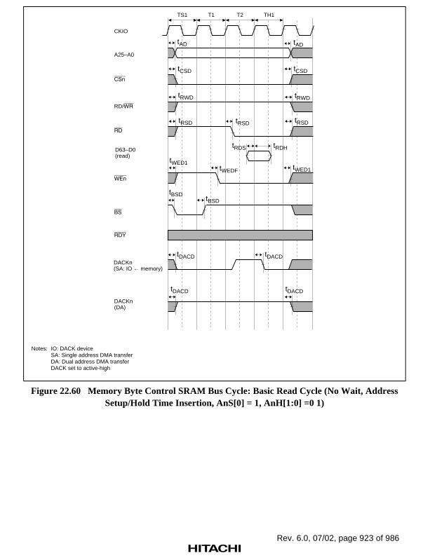
Rev. 6.0, 07/02, page 923 of 986
CKIO
RD/
D63–D0(read)
DACKn(DA)
A25–A0
TS1 T1 T2 TH1
tRSD tRSD
tWED1tWEDF tWED1
tCSD tCSD
tDACD
tBSDtBSD
tDACD
tRWD tRWD
tRSD
tAD tAD
tRDHtRDS
DACKn(SA: IO ← memory)
tDACD tDACD
Notes: IO: DACK deviceSA: Single address DMA transferDA: Dual address DMA transferDACK set to active-high
Figure 22.60 Memory Byte Control SRAM Bus Cycle: Basic Read Cycle (No Wait, AddressSetup/Hold Time Insertion, AnS[0] = 1, AnH[1:0] =0 1)

Rev. 6.0, 07/02, page 924 of 986
22.3.4 Peripheral Module Signal Timing
Table 22.36 Peripheral Module Signal Timing (1)
HD6417750RBP240
HD6417750RBP200
HD6417750RF240
HD6417750RF200
*2 *2 *2 *2
Module Item Symbol Min Max Min Max Min Max Min Max Unit Figure
TMU,RTC
Timer clockpulse width(high)
tTCLKWH
4 — 4 — 4 — 4 — Pcyc*1 22.61
Timer clockpulse width(low)
tTCLKWL
4 — 4 — 4 — 4 — Pcyc*1 22.61
Timer clockrise time
tTCLKr
— 0.8 — 0.8 — 0.8 — 0.8 Pcyc*1 22.61
Timer clockfall time
tTCLKf
— 0.8 — 0.8 — 0.8 — 0.8 Pcyc*1 22.61
Oscillationsettling time
tROSC
— 3 — 3 — 3 — 3 s 22.62
SCI Input clockcycle (asyn-chronous)
tScyc
4 — 4 — 4 — 4 — Pcyc*1 22.63
Input clockcycle (syn-chronous)
tScyc
6 — 6 — 6 — 6 — Pcyc*1 22.63
Input clockpulse width
tSCKW
0.4 0.6 0.4 0.6 0.4 0.6 0.4 0.6 tScyc
22.63
Input clockrise time
tSCKr
— 0.8 — 0.8 — 0.8 — 0.8 Pcyc*1 22.63
Input clockfall time
tSCKf
— 0.8 — 0.8 — 0.8 — 0.8 Pcyc*1 22.63
Transfer datadelay time
tTXD
1.5 5.3 1.5 6 1.5 6 1.5 6 ns 22.64
Receive datasetup time(synchronous)
tRXS
16 — 16 — 16 — 16 — ns 22.64
Receive datahold time(synchronous)
tRXH
16 — 16 — 16 — 16 — ns 22.64
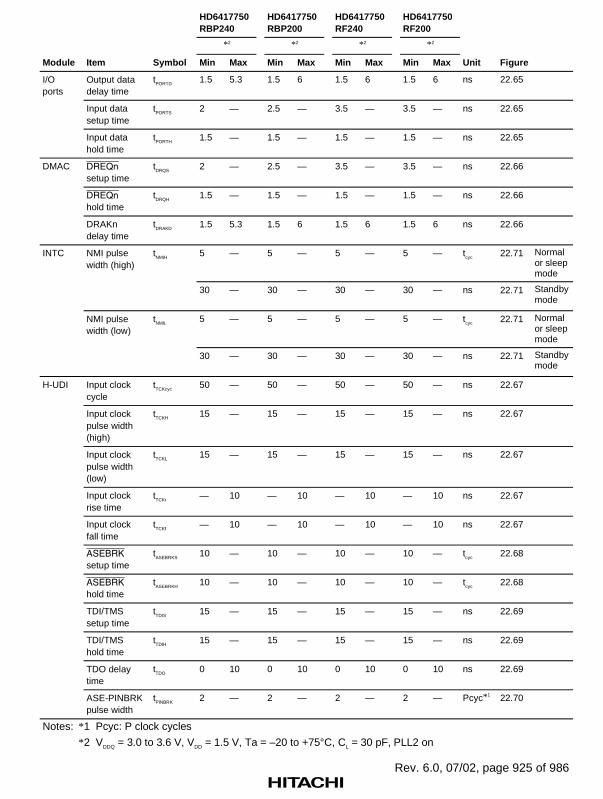
Rev. 6.0, 07/02, page 925 of 986
HD6417750RBP240
HD6417750RBP200
HD6417750RF240
HD6417750RF200
*2 *2 *2 *2
Module Item Symbol Min Max Min Max Min Max Min Max Unit Figure
I/Oports
Output datadelay time
tPORTD
1.5 5.3 1.5 6 1.5 6 1.5 6 ns 22.65
Input datasetup time
tPORTS
2 — 2.5 — 3.5 — 3.5 — ns 22.65
Input datahold time
tPORTH
1.5 — 1.5 — 1.5 — 1.5 — ns 22.65
DMAC DREQnsetup time
tDRQS
2 — 2.5 — 3.5 — 3.5 — ns 22.66
DREQnhold time
tDRQH
1.5 — 1.5 — 1.5 — 1.5 — ns 22.66
DRAKndelay time
tDRAKD
1.5 5.3 1.5 6 1.5 6 1.5 6 ns 22.66
5 — 5 — 5 — 5 — tcyc
22.71 Normalor sleepmode
NMI pulsewidth (high)
tNMIH
30 — 30 — 30 — 30 — ns 22.71 Standbymode
5 — 5 — 5 — 5 — tcyc 22.71 Normal
or sleepmode
INTC
NMI pulsewidth (low)
tNMIL
30 — 30 — 30 — 30 — ns 22.71 Standbymode
H-UDI Input clockcycle
tTCKcyc
50 — 50 — 50 — 50 — ns 22.67
Input clockpulse width(high)
tTCKH
15 — 15 — 15 — 15 — ns 22.67
Input clockpulse width(low)
tTCKL
15 — 15 — 15 — 15 — ns 22.67
Input clockrise time
tTCKr
— 10 — 10 — 10 — 10 ns 22.67
Input clockfall time
tTCKf
— 10 — 10 — 10 — 10 ns 22.67
ASEBRKsetup time
tASEBRKS
10 — 10 — 10 — 10 — tcyc
22.68
ASEBRKhold time
tASEBRKH
10 — 10 — 10 — 10 — tcyc
22.68
TDI/TMSsetup time
tTDIS
15 — 15 — 15 — 15 — ns 22.69
TDI/TMShold time
tTDIH
15 — 15 — 15 — 15 — ns 22.69
TDO delaytime
tTDO
0 10 0 10 0 10 0 10 ns 22.69
ASE-PINBRKpulse width
tPINBRK
2 — 2 — 2 — 2 — Pcyc*1 22.70
Notes: *1 Pcyc: P clock cycles
*2 VDDQ = 3.0 to 3.6 V, VDD = 1.5 V, Ta = –20 to +75°C, CL = 30 pF, PLL2 on

Rev. 6.0, 07/02, page 926 of 986
Table 22.36 Peripheral Module Signal Timing (2)
HD6417750SVF133
HD6417750SVBT133
HD6417750SF167
HD6417750SF167I
HD6417750SF200
HD6417750SBP200
*2 *3 *4
Module Item Symbol Min Max Min Max Min Max Unit Figure
TMU,RTC
Timer clockpulse width(high)
tTCLKWH
4 — 4 — 4 — Pcyc*1 22.61
Timer clockpulse width(low)
tTCLKWL
4 — 4 — 4 — Pcyc*1 22.61
Timer clockrise time
tTCLKr
— 0.8 — 0.8 — 0.8 Pcyc*1 22.61
Timer clockfall time
tTCLKf
— 0.8 — 0.8 — 0.8 Pcyc*1 22.61
Oscillationsettling time
tROSC
— 3 — 3 — 3 s 22.62
SCI Input clockcycle (asyn-chronous)
tScyc
4 — 4 — 4 — Pcyc*1 22.63
Input clockcycle (syn-chronous)
tScyc
6 — 6 — 6 — Pcyc*1 22.63
Input clockpulse width
tSCKW
0.4 0.6 0.4 0.6 0.4 0.6 tScyc
22.63
Input clockrise time
tSCKr
— 0.8 — 0.8 — 0.8 Pcyc*1 22.63
Input clockfall time
tSCKf
— 0.8 — 0.8 — 0.8 Pcyc*1 22.63
Transfer datadelay time
tTXD
1.5 10 1.5 8 1.5 6 ns 22.64
Receive datasetup time(synchronous)
tRXS
16 — 16 — 16 — ns 22.64
Receive datahold time(synchronous)
tRXH
16 — 16 — 16 — ns 22.64
I/Oports
Output datadelay time
tPORTD
1.5 10 1.5 8 1.5 6 ns 22.65
Input datasetup time
tPORTS
3.5 — 3.5 — 3 — ns 22.65
Input datahold time
tPORTH
1.5 — 1.5 — 1.5 — ns 22.65

Rev. 6.0, 07/02, page 927 of 986
HD6417750SVF133
HD6417750SVBT133
HD6417750SF167
HD6417750SF167I
HD6417750SF200
HD6417750SBP200
*2 *3 *4
Module Item Symbol Min Max Min Max Min Max Unit Figure
DMAC DREQnsetup time
tDRQS
3.5 — 3.5 — 3 — ns 22.66
DREQnhold time
tDRQH
1.5 — 1.5 — 1.5 — ns 22.66
DRAKndelay time
tDRAKD
1.5 10 1.5 8 1.5 6 ns 22.66
5 — 5 — 5 — tcyc
22.71 Normal or sleep modeNMI pulsewidth (high)
tNMIH
30 — 30 — 30 — ns 22.71 Standby mode
5 — 5 — 5 — tcyc
22.71 Normal or sleep mode
INTC
NMI pulsewidth (low)
tNMIL
30 — 30 — 30 — ns 22.71 Standby mode
H-UDI Input clockcycle
tTCKcyc
50 — 50 — 50 — ns 22.67
Input clockpulse width(high)
tTCKH
15 — 15 — 15 — ns 22.67
Input clockpulse width(low)
tTCKL
15 — 15 — 15 — ns 22.67
Input clockrise time
tTCKr
— 10 — 10 — 10 ns 22.67
Input clockfall time
tTCKf
— 10 — 10 — 10 ns 22.67
ASEBRKsetup time
tASEBRKS
10 — 10 — 10 — tcyc
22.68
ASEBRKhold time
tASEBRKH
10 — 10 — 10 — tcyc
22.68
TDI/TMSsetup time
tTDIS
15 — 15 — 15 — ns 22.69
TDI/TMShold time
tTDIH
15 — 15 — 15 — ns 22.69
TDO delaytime
tTDO
0 10 0 10 0 10 ns 22.69
ASE-PINBRKpulse width
tPINBRK
2 — 2 — 2 — Pcyc*1 22.70
Notes: *1 Pcyc: P clock cycles
*2 VDDQ = 3.0 to 3.6 V, VDD = typ. 1.5 V, Ta = –20 to +75°C, CL = 30 pF, PLL2 on
*3 VDDQ = 3.0 to 3.6 V, VDD = typ. 1.8 V, Ta = –20 to +75°C, CL = 30 pF, PLL2 on(HD6417750SF167, HD6417750SF200)
VDDQ = 3.0 to 3.6 V, VDD = typ. 1.8 V, Ta = –40 to +85°C, CL = 30 pF, PLL2 on(HD6417750SF167I)
*4 VDDQ = 3.0 to 3.6 V, VDD = typ. 1.8 V, Ta = –20 to +75°C, CL = 30 pF, PLL2 on

Rev. 6.0, 07/02, page 928 of 986
Table 22.36 Peripheral Module Signal Timing (3)
HD6417750VF128
HD6417750F167
HD6417750F167I
HD6417750BP200M
*2 *3 *4
Module Item Symbol Min Max Min Max Min Max Unit Figure
TMU,RTC
Timer clockpulse width(high)
tTCLKWH
4 — 4 — 4 — Pcyc*1 22.61
Timer clockpulse width(low)
tTCLKWL
4 — 4 — 4 — Pcyc*1 22.61
Timer clockrise time
tTCLKr
— 0.8 — 0.8 — 0.8 Pcyc*1 22.61
Timer clockfall time
tTCLKf
— 0.8 — 0.8 — 0.8 Pcyc*1 22.61
Oscillationsettling time
tROSC
— 3 — 3 — 3 s 22.62
SCI Input clockcycle (asyn-chronous)
tScyc
4 — 4 — 4 — Pcyc*1 22.63
Input clockcycle (syn-chronous)
tScyc
6 — 6 — 6 — Pcyc*1 22.63
Input clockpulse width
tSCKW
0.4 0.6 0.4 0.6 0.4 0.6 tScyc
22.63
Input clockrise time
tSCKr
— 0.8 — 0.8 — 0.8 Pcyc*1 22.63
Input clockfall time
tSCKf
— 0.8 — 0.8 — 0.8 Pcyc*1 22.63
Transfer datadelay time
tTXD
1.3 10 1.3 8 1.2 6 ns 22.64
Receive datasetup time(synchronous)
tRXS
16 — 16 — 16 — ns 22.64
Receive datahold time(synchronous)
tRXH
16 — 16 — 16 — ns 22.64
I/Oports
Output datadelay time
tPORTD
0.5 10 0.5 8 0.5 6 ns 22.65
Input datasetup time
tPORTS
3.5 — 3.5 — 3 — ns 22.65
Input datahold time
tPORTH
1.5 — 1.5 — 1.5 — ns 22.65

Rev. 6.0, 07/02, page 929 of 986
HD6417750VF128
HD6417750F167
HD6417750F167I
HD6417750BP200M
*2 *3 *4
Module Item Symbol Min Max Min Max Min Max Unit Figure
DMAC DREQnsetup time
tDRQS
3.5 — 3.5 — 3 — ns 22.66
DREQnhold time
tDRQH
1.5 — 1.5 — 1.5 — ns 22.66
DRAKndelay time
tDRAKD
1.0 10 1.0 8 1.0 6 ns 22.66
5 — 5 — 5 — tcyc
22.71 Normal or sleep modeNMI pulsewidth (high)
tNMIH
30 — 30 — 30 — ns 22.71 Standby mode
5 — 5 — 5 — tcyc
22.71 Normal or sleep mode
INTC
NMI pulsewidth (low)
tNMIL
30 — 30 — 30 — ns 22.71 Standby mode
H-UDI Input clockcycle
tTCKcyc
50 — 50 — 50 — ns 22.67
Input clockpulse width(high)
tTCKH
15 — 15 — 15 — ns 22.67
Input clockpulse width(low)
tTCKL
15 — 15 — 15 — ns 22.67
Input clockrise time
tTCKr
— 10 — 10 — 10 ns 22.67
Input clockfall time
tTCKf
— 10 — 10 — 10 ns 22.67
ASEBRKsetup time
tASEBRKS
10 — 10 — 10 — tcyc
22.68
ASEBRKhold time
tASEBRKH
10 — 10 — 10 — tcyc
22.68
TDI/TMSsetup time
tTDIS
15 — 15 — 15 — ns 22.69
TDI/TMShold time
tTDIH
15 — 15 — 15 — ns 22.69
TDO delaytime
tTDO
0 10 0 10 0 10 ns 22.69
ASE-PINBRKpulse width
tPINBRK
2 — 2 — 2 — Pcyc*1 22.70
Notes: *1 Pcyc: P clock cycles
*2 VDDQ = 3.0 to 3.6 V, VDD = typ. 1.5 V, Ta = –20 to +75°C, CL = 30 pF, PLL2 on
*3 VDDQ = 3.0 to 3.6 V, VDD = typ. 1.8 V, Ta = –20 to +75°C, CL = 30 pF, PLL2 on(HD6417750F167)
VDDQ = 3.0 to 3.6 V, VDD = typ. 1.8 V, Ta = –40 to +85°C, CL = 30 pF, PLL2 on(HD6417750F167I)
*4 VDDQ = 3.0 to 3.6 V, VDD = typ. 1.8 V, Ta = –20 to +75°C, CL = 30 pF, PLL2 on

Rev. 6.0, 07/02, page 930 of 986
TCLK
tTCLKf
tTCLKWH tTCLKWLtTCLKr
Figure 22.61 TCLK Input Timing
RTC internal clock
tROSC
Stable oscillation
VDD-RTC VDD-RTC min
Figure 22.62 RTC Oscillation Settling Time at Power-On
SCK, SCK2
tSCKf
tScyc
tSCKW
tSCKr
Figure 22.63 SCK Input Clock Timing

Rev. 6.0, 07/02, page 931 of 986
tTXD
SCK
TXD
RXD
tTXD
tRXS tRXH
tScyc
Figure 22.64 SCI I/O Synchronous Mode Clock Timing
tPORTD tPORTD
CKIO
Ports 19–0(read)
Ports 19–0(write)
tPORTS tPORTH
Figure 22.65 I/O Port Input/Output Timing
tDRAKD
tDRQHtDRQH
tDRQS tDRQS
CKIO
DRAKn
Figure 22.66(a) DREQDREQDREQDREQ/DRAK Timing

Rev. 6.0, 07/02, page 932 of 986
tDBQHtDBQS
CKIO
D63 to D0(READ)
DBREQ
BAVL
TR
tBAVDtBAVD
tTRH
(2)
tTRS
tDTRHtDTRS
(1)
(1): [2CKIO cycle – tDTRS] (= 18 ns: 100 MHz)(2): DTR = 1CKIO cycle (= 10 ns: 100 MHz) (tDTRS + tDTRH) < DTR < 10 ns
Figure 22.66(b) DBREQDBREQDBREQDBREQ/TRTRTRTR Input Timing and BAVLBAVLBAVLBAVL Output Timing
tTCKcyc
tTCKH tTCKL
tTCKrtTCKf
1/2VDDQ
VIH VIH
VIL VIL
VIH
1/2VDDQ
Note: When clock is input from TCK pin
Figure 22.67 TCK Input Timing
/BRKACK
SCK2/
tASEBRKHtASEBRKS tASEBRKS tASEBRKH
(Low)
(High)
Figure 22.68 RESETRESETRESETRESET Hold Timing

Rev. 6.0, 07/02, page 933 of 986
TDITMS
TCK
TDO
tTCKcyc
tTDO
tTDIHtTDIS
Figure 22.69 H-UDI Data Transfer Timing
tPINBRK
Figure 22.70 Pin Break Timing
tNMIH tNMIL
NMI
Figure 22.71 NMI Input Timing

Rev. 6.0, 07/02, page 934 of 986
22.3.5 AC Characteristic Test Conditions
The AC characteristic test conditions are as follows:
• Input/output signal reference level: 1.5 V (VDDQ = 3.3 ±0.3 V)
• Input pulse level: VSSQ–3.0 V (VSSQ–VDDQ for RESET, TRST, NMI, and ASEBRK/BRKACK)
• Input rise/fall time: 1 ns
The output load circuit is shown in figure 22.72.
IOL
IOH
CL VREF
LSI output pin DUT output
Notes: 1.
2.
CL is the total value, including the capacitance of the test jig, etc. The capacitance of each pin is set to 30 pF.IOL and IOH values are as shown in table 22.16, Permissible Output Currents.
Figure 22.72 Output Load Circuit

Rev. 6.0, 07/02, page 935 of 986
22.3.6 Delay Time Variation Due to Load Capacitance
A graph (reference data) of the variation in delay time when a load capacitance greater than thatstipulated (30 pF) is connected to the SH7750 Series’ pins is shown below. The graph shown infigure 22.73 should be taken into consideration if the stipulated capacitance is exceeded whenconnecting an external device.
The graph will not be linear if the connected load capacitance exceeds the range shown in figure22.73.
+4.0 ns
+3.0 ns
+2.0 ns
+1.0 ns
+0.0 ns+0 pF +25 pF +50 pF
Load Capacitance
Del
ay T
ime
Figure 22.73 Load Capacitance vs. Delay Time

Rev. 6.0, 07/02, page 936 of 986

Rev. 6.0, 07/02, page 937 of 986
Appendix A Address List
Table A.1 Address List
Module Register P4 AddressArea 7Address*1 Size
Power-OnReset
ManualReset Sleep Standby
Synchro-nizationClock
CCN PTEH H'FF00 0000 H'1F00 0000 32 Undefined Undefined Held Held Iclk
CCN PTEL H'FF00 0004 H'1F00 0004 32 Undefined Undefined Held Held Iclk
CCN TTB H'FF00 0008 H'1F00 0008 32 Undefined Undefined Held Held Iclk
CCN TEA H'FF00 000C H'1F00 000C 32 Undefined Held Held Held Iclk
CCN MMUCR H'FF00 0010 H'1F00 0010 32 H'0000 0000 H'0000 0000 Held Held Iclk
CCN BASRA H'FF00 0014 H'1F00 0014 8 Undefined Held Held Held Iclk
CCN BASRB H'FF00 0018 H'1F00 0018 8 Undefined Held Held Held Iclk
CCN CCR H'FF00 001C H'1F00 001C 32 H'0000 0000 H'0000 0000 Held Held Iclk
CCN TRA H'FF00 0020 H'1F00 0020 32 Undefined Undefined Held Held Iclk
CCN EXPEVT H'FF00 0024 H'1F00 0024 32 H'0000 0000 H'0000 0020 Held Held Iclk
CCN INTEVT H'FF00 0028 H'1F00 0028 32 Undefined Undefined Held Held Iclk
CCN PTEA H'FF00 0034 H'1F00 0034 32 Undefined Undefined Held Held Iclk
CCN QACR0 H'FF00 0038 H'1F00 0038 32 Undefined Undefined Held Held Iclk
CCN QACR1 H'FF00 003C H'1F00 003C 32 Undefined Undefined Held Held Iclk
UBC BARA H'FF20 0000 H'1F20 0000 32 Undefined Held Held Held Iclk
UBC BAMRA H'FF20 0004 H'1F20 0004 8 Undefined Held Held Held Iclk
UBC BBRA H'FF20 0008 H'1F20 0008 16 H'0000 Held Held Held Iclk
UBC BARB H'FF20 000C H'1F20 000C 32 Undefined Held Held Held Iclk
UBC BAMRB H'FF20 0010 H'1F20 0010 8 Undefined Held Held Held Iclk
UBC BBRB H'FF20 0014 H'1F20 0014 16 H'0000 Held Held Held Iclk
UBC BDRB H'FF20 0018 H'1F20 0018 32 Undefined Held Held Held Iclk
UBC BDMRB H'FF20 001C H'1F20 001C 32 Undefined Held Held Held Iclk
UBC BRCR H'FF20 0020 H'1F20 0020 16 H'0000*2 Held Held Held Iclk
BSC BCR1 H'FF80 0000 H'1F80 0000 32 H'0000 0000*2 Held Held Held Bclk
BSC BCR2 H'FF80 0004 H'1F80 0004 16 H'3FFC*2 Held Held Held Bclk
BSC BCR3*5 H'FF80 0050 H'1F80 0050 16 H'0000 Held Held Held Bclk
BSC BCR4*5 H'FE0A00F0 H'1E0A00F0 32 H'0000 0000 Held Held Held Bclk
BSC WCR1 H'FF80 0008 H'1F80 0008 32 H'7777 7777 Held Held Held Bclk
BSC WCR2 H'FF80 000C H'1F80 000C 32 H'FFFE EFFF Held Held Held Bclk

Rev. 6.0, 07/02, page 938 of 986
Table A.1 Address List (cont)
Module Register P4 AddressArea 7Address*1 Size
Power-OnReset
ManualReset Sleep Standby
Synchro-nizationClock
BSC WCR3 H'FF80 0010 H'1F80 0010 32 H'0777 7777 Held Held Held Bclk
BSC MCR H'FF80 0014 H'1F80 0014 32 H'0000 0000 Held Held Held Bclk
BSC PCR H'FF80 0018 H'1F80 0018 16 H'0000 Held Held Held Bclk
BSC RTCSR H'FF80 001C H'1F80 001C 16 H'0000 Held Held Held Bclk
BSC RTCNT H'FF80 0020 H'1F80 0020 16 H'0000 Held Held Held Bclk
BSC RTCOR H'FF80 0024 H'1F80 0024 16 H'0000 Held Held Held Bclk
BSC RFCR H'FF80 0028 H'1F80 0028 16 H'0000 Held Held Held Bclk
BSC PCTRA H'FF80 002C H'1F80 002C 32 H'0000 0000 Held Held Held Bclk
BSC PDTRA H'FF80 0030 H'1F80 0030 16 Undefined Held Held Held Bclk
BSC PCTRB H'FF80 0040 H'1F80 0040 32 H'0000 0000 Held Held Held Bclk
BSC PDTRB H'FF80 0044 H'1F80 0044 16 Undefined Held Held Held Bclk
BSC GPIOIC H'FF80 0048 H'1F80 0048 16 H'0000 0000 Held Held Held Bclk
BSC SDMR2 H'FF90 xxxx H'1F90 xxxx 8 Write-only Bclk
BSC SDMR3 H'FF94 xxxx H'1F94 xxxx 8 Bclk
DMAC SAR0 H'FFA0 0000 H'1FA0 0000 32 Undefined Undefined Held Held Bclk
DMAC DAR0 H'FFA0 0004 H'1FA0 0004 32 Undefined Undefined Held Held Bclk
DMAC DMATCR0 H'FFA0 0008 H'1FA0 0008 32 Undefined Undefined Held Held Bclk
DMAC CHCR0 H'FFA0 000C H'1FA0 000C 32 H'0000 0000 H'0000 0000 Held Held Bclk
DMAC SAR1 H'FFA0 0010 H'1FA0 0010 32 Undefined Undefined Held Held Bclk
DMAC DAR1 H'FFA0 0014 H'1FA0 0014 32 Undefined Undefined Held Held Bclk
DMAC DMATCR1 H'FFA0 0018 H'1FA0 0018 32 Undefined Undefined Held Held Bclk
DMAC CHCR1 H'FFA0 001C H'1FA0 001C 32 H'0000 0000 H'0000 0000 Held Held Bclk
DMAC SAR2 H'FFA0 0020 H'1FA0 0020 32 Undefined Undefined Held Held Bclk
DMAC DAR2 H'FFA0 0024 H'1FA0 0024 32 Undefined Undefined Held Held Bclk
DMAC DMATCR2 H'FFA0 0028 H'1FA0 0028 32 Undefined Undefined Held Held Bclk
DMAC CHCR2 H'FFA0 002C H'1FA0 002C 32 H'0000 0000 H'0000 0000 Held Held Bclk
DMAC SAR3 H'FFA0 0030 H'1FA0 0030 32 Undefined Undefined Held Held Bclk
DMAC DAR3 H'FFA0 0034 H'1FA0 0034 32 Undefined Undefined Held Held Bclk
DMAC DMATCR3 H'FFA0 0038 H'1FA0 0038 32 Undefined Undefined Held Held Bclk
DMAC CHCR3 H'FFA0 003C H'1FA0 003C 32 H'0000 0000 H'0000 0000 Held Held Bclk
DMAC DMAOR H'FFA0 0040 H'1FA0 0040 32 H'0000 0000 H'0000 0000 Held Held Bclk

Rev. 6.0, 07/02, page 939 of 986
Table A.1 Address List (cont)
Module Register P4 AddressArea 7Address*1 Size
Power-OnReset
ManualReset Sleep Standby
Synchro-nizationClock
DMAC SAR4*5 H'FFA0 0050 H'1FA0 0050 32 Undefined Undefined Held Held Bclk
DMAC DAR4*5 H'FFA0 0054 H'1FA0 0054 32 Undefined Undefined Held Held Bclk
DMAC DMATCR4*5 H'FFA0 0058 H'1FA0 0058 32 Undefined Undefined Held Held Bclk
DMAC CHCR4*5 H'FFA0 005C H'1FA0 005C 32 H'0000 0000 H'0000 0000 Held Held Bclk
DMAC SAR5*5 H'FFA0 0060 H'1FA0 0060 32 Undefined Undefined Held Held Bclk
DMAC DAR5*5 H'FFA0 0064 H'1FA0 0064 32 Undefined Undefined Held Held Bclk
DMAC DMATCR5*5 H'FFA0 0068 H'1FA0 0068 32 Undefined Undefined Held Held Bclk
DMAC CHCR5*5 H'FFA0 006C H'1FA0 006C 32 H'0000 0000 H'0000 0000 Held Held Bclk
DMAC SAR6*5 H'FFA0 0070 H'1FA0 0070 32 Undefined Undefined Held Held Bclk
DMAC DAR6*5 H'FFA0 0074 H'1FA0 0074 32 Undefined Undefined Held Held Bclk
DMAC DMATCR6*5 H'FFA0 0078 H'1FA0 0078 32 Undefined Undefined Held Held Bclk
DMAC CHCR6*5 H'FFA0 007C H'1FA0 007C 32 H'0000 0000 H'0000 0000 Held Held Bclk
DMAC SAR7*5 H'FFA0 0080 H'1FA0 0080 32 Undefined Undefined Held Held Bclk
DMAC DAR7*5 H'FFA0 0084 H'1FA0 0084 32 Undefined Undefined Held Held Bclk
DMAC DMATCR7*5 H'FFA0 0088 H'1FA0 0088 32 Undefined Undefined Held Held Bclk
DMAC CHCR7*5 H'FFA0 008C H'1FA0 008C 32 H'0000 0000 H'0000 0000 Held Held Bclk
CPG FRQCR H'FFC0 0000 H'1FC0 0000 16 *2 Held Held Held Pclk
CPG*6 STBCR H'FFC0 0004 H'1FC0 0004 8 H'00 Held Held Held Pclk
CPG*6 WTCNT H'FFC0 0008 H'1FC0 0008 8/16*3 H'00 Held Held Held Pclk
CPG*6 WTCSR H'FFC0 000C H'1FC0 000C 8/16*3 H'00 Held Held Held Pclk
CPG*6 STBCR2 H'FFC0 0010 H'1FC0 0010 8 H'00 Held Held Held Pclk
RTC R64CNT H'FFC8 0000 H'1FC8 0000 8 Held Held Held Held Pclk
RTC RSECCNT H'FFC8 0004 H'1FC8 0004 8 Held Held Held Held Pclk
RTC RMINCNT H'FFC8 0008 H'1FC8 0008 8 Held Held Held Held Pclk
RTC RHRCNT H'FFC8 000C H'1FC8 000C 8 Held Held Held Held Pclk
RTC RWKCNT H'FFC8 0010 H'1FC8 0010 8 Held Held Held Held Pclk
RTC RDAYCNT H'FFC8 0014 H'1FC8 0014 8 Held Held Held Held Pclk
RTC RMONCNTH'FFC8 0018 H'1FC8 0018 8 Held Held Held Held Pclk
RTC RYRCNT H'FFC8 001C H'1FC8 001C 16 Held Held Held Held Pclk
RTC RSECAR H'FFC8 0020 H'1FC8 0020 8 Held *2 Held Held Held Pclk
RTC RMINAR H'FFC8 0024 H'1FC8 0024 8 Held *2 Held Held Held Pclk

Rev. 6.0, 07/02, page 940 of 986
Table A.1 Address List (cont)
Module Register P4 AddressArea 7Address*1 Size
Power-OnReset
ManualReset Sleep Standby
Synchro-nizationClock
RTC RHRAR H'FFC8 0028 H'1FC8 0028 8 Held *2 Held Held Held Pclk
RTC RWKAR H'FFC8 002C H'1FC8 002C 8 Held *2 Held Held Held Pclk
RTC RDAYAR H'FFC8 0030 H'1FC8 0030 8 Held *2 Held Held Held Pclk
RTC RMONAR H'FFC8 0034 H'1FC8 0034 8 Held *2 Held Held Held Pclk
RTC RCR1 H'FFC8 0038 H'1FC8 0038 8 H'00*2 H'00*2 Held Held Pclk
RTC RCR2 H'FFC8 003C H'1FC8 003C 8 H'09*2 H'00*2 Held Held Pclk
RTC RCR3*5 H'FFC8 0050 H'1FC8 0050 8 H'00 Held Held Held Pclk
RTC RYRAR*5 H'FFC8 0054 H'1FC8 0054 16 Undefined Held Held Held Pclk
INTC ICR H'FFD0 0000 H'1FD0 0000 16 H'0000*2 H'0000*2 Held Held Pclk
INTC IPRA H'FFD0 0004 H'1FD0 0004 16 H'0000 H'0000 Held Held Pclk
INTC IPRB H'FFD0 0008 H'1FD0 0008 16 H'0000 H'0000 Held Held Pclk
INTC IPRC H'FFD0 000C H'1FD0 000C 16 H'0000 H'0000 Held Held Pclk
INTC IPRD*4 H'FFD00010 H'1F000010 16 H'DA74 H'DA74 Held Held Pclk
INTC INTPRI00*5
H'FE08 0000 H'1E08 0000 32 H'0000 0000 Held Held Held Pclk
INTC INTREQ00*5
H'FE08 0020 H'1E08 0020 32 H'0000 0000 Held Held Held Pclk
INTC INTMSK00*5
H'FE08 0040 H'1E08 0040 32 H'0000 0300 Held Held Held Pclk
INTC INTMSKCLR00*5
H'FE08 0060 H'1E08 0060 32 Write-only Pclk
CPG*6 CLKSTP00*5
H'FE0A 0000 H'1E0A 0000 32 H'0000 0000 Held Held Held Pclk
CPG*6 CLKSTPCLR00*5
H'FE0A 0008 H'1E0A 0008 32 Write-only Pclk
TMU TSTR2*5 H'FE10 0004 H'1E10 0004 8 H'00 Held Held Held Pclk
TMU TCOR3*5 H'FE10 0008 H'1E10 0008 32 H'FFFF FFFF Held Held Held Pclk
TMU TCNT3*5 H'FE10 000C H'1E10 000C 32 H'FFFF FFFF Held Held Held Pclk
TMU TCR3*5 H'FE10 0010 H'1E10 0010 16 H'0000 Held Held Held Pclk
TMU TCOR4*5 H'FE10 0014 H'1E10 0014 32 H'FFFF FFFF Held Held Held Pclk
TMU TCNT4*5 H'FE10 0018 H'1E10 0018 32 H'FFFF FFFF Held Held Held Pclk
TMU TCR4*5 H'FE10 001C H'1E10 001C 16 H'0000 Held Held Held Pclk

Rev. 6.0, 07/02, page 941 of 986
Table A.1 Address List (cont)
Module Register P4 AddressArea 7Address*1 Size
Power-OnReset
ManualReset Sleep Standby
Synchro-nizationClock
TMU TOCR H'FFD8 0000 H'1FD8 0000 8 H'00 H'00 Held Held Pclk
TMU TSTR H'FFD8 0004 H'1FD8 0004 8 H'00 H'00 Held H'00*2 Pclk
TMU TCOR0 H'FFD8 0008 H'1FD8 0008 32 H'FFFF FFFF H'FFFF FFFF Held Held Pclk
TMU TCNT0 H'FFD8 000C H'1FD8 000C 32 H'FFFF FFFF H'FFFF FFFF Held Held Pclk
TMU TCR0 H'FFD8 0010 H'1FD8 0010 16 H'0000 H'0000 Held Held Pclk
TMU TCOR1 H'FFD8 0014 H'1FD8 0014 32 H'FFFF FFFF H'FFFF FFFF Held Held Pclk
TMU TCNT1 H'FFD8 0018 H'1FD8 0018 32 H'FFFF FFFF H'FFFF FFFF Held Held Pclk
TMU TCR1 H'FFD8 001C H'1FD8 001C 16 H'0000 H'0000 Held Held Pclk
TMU TCOR2 H'FFD8 0020 H'1FD8 0020 32 H'FFFF FFFF H'FFFF FFFF Held Held Pclk
TMU TCNT2 H'FFD8 0024 H'1FD8 0024 32 H'FFFF FFFF H'FFFF FFFF Held Held Pclk
TMU TCR2 H'FFD8 0028 H'1FD8 0028 16 H'0000 H'0000 Held Held Pclk
TMU TCPR2 H'FFD8 002C H'1FD8 002C 32 Held Held Held Held Pclk
SCI SCSMR1 H'FFE0 0000 H'1FE0 0000 8 H'00 H'00 Held H'00 Pclk
SCI SCBRR1 H'FFE0 0004 H'1FE0 0004 8 H'FF H'FF Held H'FF Pclk
SCI SCSCR1 H'FFE0 0008 H'1FE0 0008 8 H'00 H'00 Held H'00 Pclk
SCI SCTDR1 H'FFE0 000C H'1FE0 000C 8 H'FF H'FF Held H'FF Pclk
SCI SCSSR1 H'FFE0 0010 H'1FE0 0010 8 H'84 H'84 Held H'84 Pclk
SCI SCRDR1 H'FFE0 0014 H'1FE0 0014 8 H'00 H'00 Held H'00 Pclk
SCI SCSCMR1 H'FFE0 0018 H'1FE0 0018 8 H'00 H'00 Held H'00 Pclk
SCI SCSPTR1 H'FFE0 001C H'1FE0 001C 8 H'00*2 H'00*2 Held H'00*2 Pclk
SCIF SCSMR2 H'FFE8 0000 H'1FE8 0000 16 H'0000 H'0000 Held Held Pclk
SCIF SCBRR2 H'FFE8 0004 H'1FE8 0004 8 H'FF H'FF Held Held Pclk
SCIF SCSCR2 H'FFE8 0008 H'1FE8 0008 16 H'0000 H'0000 Held Held Pclk
SCIF SCFTDR2 H'FFE8 000C H'1FE8 000C 8 Undefined Undefined Held Held Pclk
SCIF SCFSR2 H'FFE8 0010 H'1FE8 0010 16 H'0060 H'0060 Held Held Pclk
SCIF SCFRDR2 H'FFE8 0014 H'1FE8 0014 8 Undefined Undefined Held Held Pclk
SCIF SCFCR2 H'FFE8 0018 H'1FE8 0018 16 H'0000 H'0000 Held Held Pclk
SCIF SCFDR2 H'FFE8 001C H'1FE8 001C 16 H'0000 H'0000 Held Held Pclk
SCIF SCSPTR2 H'FFE8 0020 H'1FE8 0020 16 H'0000*2 H'0000*2 Held Held Pclk
SCIF SCLSR2 H'FFE8 0024 H'1FE8 0024 16 H'0000 H'0000 Held Held Pclk

Rev. 6.0, 07/02, page 942 of 986
Table A.1 Address List (cont)
Module Register P4 AddressArea 7Address*1 Size
Power-OnReset
ManualReset Sleep Standby
Synchro-nizationClock
H-UDI SDIR H'FFF0 0000 H'1FF0 0000 16 H'FFFF*2 Held Held Held Pclk
H-UDI SDDR H'FFF0 0008 H'1FF0 0008 32 Undefined Held Held Held Pclk
H-UDI SDINT*5 H'FFF0 0014 H'1FF0 0014 16 H'0000 Held Held Held Pclk
Notes: *1 With control registers, the above addresses in the physical page number field can beaccessed by means of a TLB setting. When these addresses are referenced directlywithout using the TLB, operations are limited.
*2 Includes undefined bits. See the descriptions of the individual modules.*3 Use word-size access when writing. Perform the write with the upper byte set to H'5A or
H'A5, respectively. Byte- and longword-size writes cannot be used.
Use byte-size access when reading.*4 SH7750S, SH7750R only*5 SH7750R only
*6 Includes power-down states

Rev. 6.0, 07/02, page 943 of 986
Appendix B Package Dimensions
0.635 1.27
0.63
51.
27
27.0
27.0
0.20 (× 4)
A B2.
1
0.6
± 0
.1
0.35 C
C
0.20 C
Details of the part A
256 × φ0.75 ± 0.150.30 C BAM
0.10 CM
Y
V
TP
M
KH
F
D
B
W
UR
N
L
J
G
ECA
A1 3 5 7 9 11 13 15 17 19
2 4 6 8 10 12 14 16 18 20
Hitachi CodeJEDECJEITAMass (reference value)
BP-256Conforms—3.0 g
Unit: mm
Figure B.1 Package Dimensions (256-Pin BGA) (SH7750 and SH7750S)

Rev. 6.0, 07/02, page 944 of 986
0.635 1.270.
635
1.27
27.0
27.0
0.20 (× 4)
A B2.
1
0.6
± 0
.1
0.35 C
C
0.20 C
Details of the part A
256 × φ0.75 ± 0.150.30 C BAM
0.10 CM
Y
V
TP
M
KH
F
D
B
W
UR
N
L
J
G
ECA
A1 3 5 7 9 11 13 15 17 19
2 4 6 8 10 12 14 16 18 20
Hitachi CodeJEDECJEITAMass (reference value)
BP-256AConforms—3.0 g
Unit: mm
Figure B.2 Package Dimensions (256-Pin BGA) (SH7750R Only)

Rev. 6.0, 07/02, page 945 of 986
Hitachi CodeJEDECJEITAMass (reference value)
FP-208E—Conforms5.3 g
*Dimension including the plating thicknessBase material dimension
30.6 ± 0.2
30.6
± 0
.2
0.5
3.56
Max
0˚ – 8˚
*0.1
7 ±
0.0
5
156 105
104
521
157
208 53
*0.22 ± 0.050.10 M
0.10
3.20
0.5 ± 0.1
1.3
28
0.15
+0.
10–0
.15
1.250.20 ± 0.04
0.15
± 0
.04
Unit: mm
Figure B.3 Package Dimensions (208-Pin QFP)

Rev. 6.0, 07/02, page 946 of 986
0.80
1.10
1.10
15.00
15.0
0
0.154 ×
0.2 CC
0.10 C
0.80
0.40
± 0
.05
1.40
Max
BA
DC
FE
HG
KJ
ML
PN
TR
U
17 1516
1314
1112
910
78
56
34
12
Hitachi CodeJEDECJEITAMass (reference value)
BP-264––0.6 g
0.20 C A
0.20
CB
B
Cφ0.08 A B264 × φ0.50 ± 0.05
M
A
Unit: mm
Figure B.4 Package Dimensions (264-Pin CSP)

Rev. 6.0, 07/02, page 947 of 986
Appendix C Mode Pin Settings
The MD8–MD0 pin values are input in the event of a power-on reset via the RESET orSCK2/MRESET pin.
(1) Clock Modes
• Clock Operating Modes (SH7750, SH7750S)External
Pin CombinationFrequency
(vs. Input Clock)
ClockOperatingMode MD2 MD1 MD0
1/2FrequencyDivider PLL1 PLL2
CPUClock
BusClock
PeripheralModuleClock
FRQCRInitial Value
0 0 Off On On 6 3/2 3/2 H'0E1A
1
0
1 Off On On 6 1 1 H'0E23
2 0 On On On 3 1 1/2 H'0E13
3
0
1
1 Off On On 6 2 1 H'0E13
4 0 On On On 3 3/2 3/4 H'0E0A
5
1 0
1 Off On On 6 3 3/2 H'0E0A
Notes: 1. Turning on/off of the ½ frequency divider is solely determined by the clock operatingmode.
2. For the ranges of input clock frequency, see the descriptions of the EXTAL clock inputfrequency (fEX) and CKIO clock output (fOP) in section 22.3.1, Clock and Control SignalTiming.
• Clock Operating Modes (SH7750R)External
Pin CombinationFrequency
(vs. Input Clock)ClockOperatingMode MD2 MD1 MD0 PLL1 PLL2
CPUClock
BusClock
PeripheralModule Clock
FRQCRInitial Value
0 0 On (×12) On 12 3 3 H'0E1A
1
0
1 On (×12) On 12 3/2 3/2 H'0E2C
2 0 On (×6) On 6 2 1 H'0E13
3
0
1
1 On (×12) On 12 4 2 H'0E13
4 0 On (×6) On 6 3 3/2 H'0E0A
5
0
1 On (×12) On 12 6 3 H'0E0A
6
1
1 0 Off (×6) Off 1 1/2 1/2 H'0808
Notes: 1. The multiplication factor of PLL 1 is solely determined by the clock operating mode.2. For the ranges of input clock frequency, see the descriptions of the EXTAL clock input
frequency (fEX) and CKIO clock output (fOP) in section 22.3.1, Clock and Control SignalTiming.

Rev. 6.0, 07/02, page 948 of 986
(2) Area 0 Bus Width
Pin Value
MD6 MD4 MD3 Bus Width Memory Type
0 0 0 64 bits MPX interface
1 8 bits Reserved (setting prohibited)
1 0 16 bits Reserved
1 32 bits MPX interface
1 0 0 64 bits SRAM interface
1 8 bits SRAM interface
1 0 16 bits SRAM interface
1 32 bits SRAM interface
(3) Endian
Pin Value
MD5 Endian
0 Big endian
1 Little endian
(4) Master/Slave
Pin Value
MD7 Master/Slave
0 Slave
1 Master
(5) Clock Input
Pin Value
MD8 Clock Input
0 External input clock
1 Crystal resonator

Rev. 6.0, 07/02, page 949 of 986
Appendix D CKIO2ENB Pin Configuration
rd_pullup_control
rd_dt_
rd_hiz_control
rdwr_pullup_control
rdwr_dt_
rdwr_hiz_control
Bus clock
ckio_hiz_control
VSSQ
CKIO2
CKIO
RD/
RD/
/ /
VDDQ
VDDQ
VDDQ
VDDQ
VDDQSH7750 Series
PLL2
Figure D.1 CKIO2ENBCKIO2ENBCKIO2ENBCKIO2ENB Pin Configuration
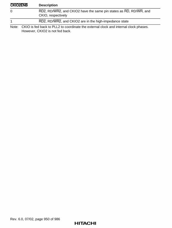
Rev. 6.0, 07/02, page 950 of 986
CKIO2ENBCKIO2ENBCKIO2ENBCKIO2ENB Description
0 RD2, RD/WR2, and CKIO2 have the same pin states as RD, RD/WR, andCKIO, respectively
1 RD2, RD/WR2, and CKIO2 are in the high-impedance state
Note: CKIO is fed back to PLL2 to coordinate the external clock and internal clock phases.However, CKIO2 is not fed back.

Rev. 6.0, 07/02, page 951 of 986
Appendix E Pin Functions
E.1 Pin States
Table E.1 Pin States in Reset, Power-Down State, and Bus-Released State
Reset(Power-On)
Reset(Manual)
Signal Name I/O Master Slave Master Slave StandbyBusReleased
Hard-wareStandby Notes
D0–D7 I/O Z*15 Z*15 Z*15 Z*15 Z*15 Z*15 Z
D8–D15 I/O Z*15 Z*15 Z*15 Z*15 Z*15 Z*15 Z
D16–D23 I/O Z*15 Z*15 Z*15 Z*15 Z*15 Z*15 Z
D24–D31 I/O Z*15 Z*15 Z*15 Z*15 Z*15 Z*15 Z
D32–D51 I/O Z*15 Z*15 ZK *15 ZK *15 Z*15K Z*15K Z Outputstate heldwhen usedas port
D52–D55 I/O Z*15 Z*15 Z*15 Z*15 Z*15 Z*15 Z
D56–D63 I/O Z*15 Z*15 Z*15 Z*15 Z*15 Z*15 Z
A0, A1, A18–A25 O Z*16 Z*16 Z*14O*17 Z*14 Z*14O*7 Z*14 Z
A2–A17 O Z*16 Z*16 Z*14O*9 Z*14 Z*14O*7 Z*14 Z
RESET I I I I I I I I
BACK/BSREQ O H H H H H O Z
BREQ/BSACK I I*16 I*16 I*13 I*13 I*13 I*13 I
BS O H Z*16 H Z*14 Z*14H*7 Z*14 Z
CKE O H H O*6 O*6 L O*6 Z
CS6–CS0 O H Z*16 H Z*14 Z*14H*7 Z*14 Z
RAS O H Z*16 O*6 Z*14 Z*14O*5 Z*14O*5 Z
RD/CASS O H Z*16 O*6 Z*14 Z*14O*5 Z*14O*5 Z
RD/WR O H Z*16 H Z*14 Z*14H*7 Z*14 Z
RDY I PI*16 PI*16 I*13 I*13 I*13 I*13 I
WE7/CAS7/DQM7 O H Z*16 O*6 Z*14 Z*14O*5 Z*14O*5 Z
WE6/CAS6/DQM6 O H Z*16 O*6 Z*14 Z*14O*5 Z*14O*5 Z
WE5/CAS5/DQM5 O H Z*16 O*6 Z*14 Z*14O*5 Z*14O*5 Z
WE4/CAS4/DQM4 O H Z*16 O*6 Z*14 Z*14O*5 Z*14O*5 Z
WE3/CAS3/DQM3 O H Z*16 O*6 Z*14 Z*14O*5 Z*14O*5 Z

Rev. 6.0, 07/02, page 952 of 986
Table E.1 Pin States in Reset, Power-Down State, and Bus-Released State (cont)
Reset(Power-On)
Reset(Manual)
Signal Name I/O Master Slave Master Slave StandbyBusReleased
Hard-wareStandby Notes
WE2/CAS2/DQM2 O H Z*16 O*6 Z*14 Z*14O*5 Z*14O*5 Z
WE1/CAS1/DQM1 O H Z*16 O*6 Z*14 Z*14O*5 Z*14O*5 Z
WE0/CAS0/DQM0 O H Z*16 O*6 Z*14 Z*14O*5 Z*14O*5 Z
DACK1–DACK0 O L L L L Z*12O*8 O*12 Z DMAC
MD7/TXD I/O I*16 I*16 Z*12 Z*12 Z*12O*8 Z*12O Z SCI
MD6/IOIS16 I I*16 I*16 I*13 I*13 I*13 I*13 I PCMCIA(I/O)
MD5/RAS2 I/O*1 I*16 I*16 Z*13O*6 Z*13 Z*13O*5 Z*13O*5 Z DRAM2
MD4/CE2B I/O*2 I*16 I*16 Z*13H Z*13 Z*13H*7 Z*13 Z PCMCIA
MD3/CE2A I/O*3 I*16 I*16 Z*13H Z*13 Z*13H*7 Z*13 Z PCMCIA
CKIO O O O ZO*11 ZO*11 ZO*11 ZO*11 Z
STATUS1–STATUS0
O O O O O O O Z*18
IRL3–IRL0 I PI*16 PI*16 I*13 I*13 I*13 I*13 I INTC
NMI I PI*16 PI*16 I*13 I*13 I*13 I*13 I INTC
DREQ1–DREQ0 I PI*16 PI*16 I*12 I*12 I*12 I*12 I DMAC
DRAK1–DRAK0 O L L L L Z*12O*8 O*12 Z DMAC
MD0/SCK I/O I*16 I*16 I*12 I*12 I*12Z*12O*8 I*12O Z SCI
RXD I PI*16 PI*16 I*12 I*12 I*12 I*12 I SCI
SCK2/MRESET I PI*16 PI*16 I*12 I*12 I*12 I*12 I SCIF
MD1/TXD2 I/O I*16 I*16 Z*12 Z*12 Z*12O*8 Z*12O Z SCIF
MD2/RXD2 I I*16 I*16 I*12 I*12 I*12 I*12 I SCIF
CTS2 I/O PI*16 PI*16 I*12 I*12 I*12Z*12O*8 I*12O Z SCIF
MD8/RTS2 I/O I*16 I*16 I*12 I*12 I*12Z*12O*8 I*12O Z SCIF
TCLK I/O PI*16 PI*16 I*12 I*12 I*12O I*12O Z TMU
TDO O O O O O O O Z H-UDI
TMS I PI*16 PI*16 I*16 I*16 I*16 I*16 I H-UDI
TCK I PI*16 PI*16 I*16 I*16 I*16 I*16 I H-UDI
TDI I PI*16 PI*16 I*16 I*16 I*16 I*16 I H-UDI
TRST I PI*16 PI*16 I*16 I*16 I*16 I*16 I H-UDI
CKIO2*10 O O O ZO*11 ZO*11 ZO*11 ZO*11 Z

Rev. 6.0, 07/02, page 953 of 986
Table E.1 Pin States in Reset, Power-Down State, and Bus-Released State (cont)
Reset(Power-On)
Reset(Manual)
Signal Name I/O Master Slave Master Slave StandbyBusReleased
Hard-wareStandby Notes
RD2*10 O H Z*16 O*6 Z*14 Z*14O*5 Z*14O*5 Z
RD/WR2*10 O H Z*16 H Z*14 Z*14H*7 Z*14 Z
CKIO2ENB I I I I I I I I
CA I I I I I I I I
Notes: I: InputO: OutputH: High-level output
L: Low-level outputZ: High-impedance
K: Output state held
*1 Output when area 2 DRAM is used.
*2 Output when area 5 PCMCIA is used.*3 Output when area 6 PCMCIA is used.*4 Depends on refresh and DMAC operations.
*5 Z (I) or O (refresh), depending on register setting (BCR1.HIZCNT).*6 Depends on refresh operation.*7 Z (I) or H (state held), depending on register setting (BCR1.HIZMEM).
*8 Z or O, depending on register setting (STBCR.PHZ).*9 Output when refreshing is set.*10 Operation in respective state when CKIO2ENB = 0; Z when CKIO2ENB = 1.
*11 Z or O, depending on register setting (FRQCR.CKOEN).*12 Pulled up or not pulled up, depending on register setting (STBCR.PPU).*13 Pulled up or not pulled up, depending on register setting (BCR1.IPUP).
*14 Pulled up or not pulled up, depending on register setting (BCR1.OPUP).*15 Not pulled up.*16 Pulled up with a built-in pull-up resistance. However, cannot be used for MD pin pull-
up in a power-on reset. Pull up or down outside the SH-4.*17 Output when refreshing is set (SH7750R only).
*18 Z or O, depending on register setting (STBCR2.STHZ) (SH7750R only).

Rev. 6.0, 07/02, page 954 of 986
E.2 Handling of Unused Pins
• When RTC is not used
EXTAL2: Pull up to 3.3 V
XTAL2: Leave unconnected
VDD-RTC: Power supply (3.3 V)
VSS-RTC: Power supply (0 V)
• When PLL1 is not used
VDD-PLL1: Power supply (3.3 V)
VSS-PLL1: Power supply (0 V)
• When PLL2 is not used
VDD-PLL2: Power supply (3.3 V)
VSS-PLL2: Power supply (0 V)
• When on-chip crystal oscillator is not used
XTAL: Leave unconnected
VDD-CPG: Power supply (3.3 V)
VSS-CPG: Power supply (0 V)

Rev. 6.0, 07/02, page 955 of 986
Appendix F Synchronous DRAM AddressMultiplexing Tables
(1) BUS 64 (16M: 512k × 16b × 2) × 4 *AMX 0 AMXEXT 0 16M, column-addr-8bit 8MB
SH7750 Series Address Pins
RAS Cycle CAS Cycle
Synchronous DRAMAddress Pins
Function
A14 A22 A22 A11 BANK selects bank address
A13 A21 H/L A10 Address precharge setting
A12 A20 0 A9
A11 A19 0 A8
A10 A18 A10 A7
A9 A17 A9 A6
A8 A16 A8 A5
A7 A15 A7 A4
A6 A14 A6 A3
A5 A13 A5 A2
A4 A12 A4 A1
A3 A11 A3 A0
Address
A2 Not used
A1 Not used
A0 Not used

Rev. 6.0, 07/02, page 956 of 986
(2) BUS 32 (16M: 512k × 16b × 2) × 2 *AMX 0 AMXEXT 0 16M, column-addr-8bit 4MB
SH7750 Series Address Pins
RAS Cycle CAS CycleSynchronous DRAM
Address PinsFunction
A14
A13 A21 A21 A11 BANK selects bank address
A12 A20 H/L A10 Address precharge setting
A11 A19 0 A9
A10 A18 0 A8
A9 A17 A9 A7
A8 A16 A8 A6
A7 A15 A7 A5
A6 A14 A6 A4
A5 A13 A5 A3
A4 A12 A4 A2
A3 A11 A3 A1
A2 A10 A2 A0
Address
A1 Not used
A0 Not used

Rev. 6.0, 07/02, page 957 of 986
(3) BUS 64 (16M: 512k × 16b × 2) × 4 *AMX 0 AMXEXT 1 16M, column-addr-8bit 8MB
SH7750 Series Address Pins
RAS Cycle CAS CycleSynchronous DRAM
Address PinsFunction
A14 A21 A21 A11 BANK selects bank address
A13 A22 H/L A10 Address precharge setting
A12 A20 0 A9
A11 A19 0 A8
A10 A18 A10 A7
A9 A17 A9 A6
A8 A16 A8 A5
A7 A15 A7 A4
A6 A14 A6 A3
A5 A13 A5 A2
A4 A12 A4 A1
A3 A11 A3 A0
Address
A2 Not used
A1 Not used
A0 Not used
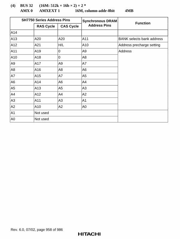
Rev. 6.0, 07/02, page 958 of 986
(4) BUS 32 (16M: 512k × 16b × 2) × 2 *AMX 0 AMXEXT 1 16M, column-addr-8bit 4MB
SH7750 Series Address Pins
RAS Cycle CAS CycleSynchronous DRAM
Address PinsFunction
A14
A13 A20 A20 A11 BANK selects bank address
A12 A21 H/L A10 Address precharge setting
A11 A19 0 A9
A10 A18 0 A8
A9 A17 A9 A7
A8 A16 A8 A6
A7 A15 A7 A5
A6 A14 A6 A4
A5 A13 A5 A3
A4 A12 A4 A2
A3 A11 A3 A1
A2 A10 A2 A0
Address
A1 Not used
A0 Not used

Rev. 6.0, 07/02, page 959 of 986
(5) BUS 64 (16M: 1M × 8b × 2) × 8 *AMX 1 AMXEXT 0 16M, column-addr-9bit 16MB
SH7750 Series Address Pins
RAS Cycle CAS CycleSynchronous DRAM
Address PinsFunction
A14 A23 A23 A11 BANK selects bank address
A13 A22 H/L A10 Address precharge setting
A12 A21 0 A9
A11 A20 A11 A8
A10 A19 A10 A7
A9 A18 A9 A6
A8 A17 A8 A5
A7 A16 A7 A4
A6 A15 A6 A3
A5 A14 A5 A2
A4 A13 A4 A1
A3 A12 A3 A0
Address
A2 Not used
A1 Not used
A0 Not used

Rev. 6.0, 07/02, page 960 of 986
(6) BUS 32 (16M: 1M × 8b × 2) × 4 *AMX 1 AMXEXT 0 16M, column-addr-9bit 8MB
SH7750 Series Address Pins
RAS Cycle CAS CycleSynchronous DRAM
Address PinsFunction
A14
A13 A22 A22 A11 BANK selects bank address
A12 A21 H/L A10 Address precharge setting
A11 A20 0 A9
A10 A19 A10 A8
A9 A18 A9 A7
A8 A17 A8 A6
A7 A16 A7 A5
A6 A15 A6 A4
A5 A14 A5 A3
A4 A13 A4 A2
A3 A12 A3 A1
A2 A11 A2 A0
Address
A1 Not used
A0 Not used

Rev. 6.0, 07/02, page 961 of 986
(7) BUS 64 (16M: 1M × 8b × 2) × 8 *AMX 1 AMXEXT 1 16M, column-addr-9bit 16MB
SH7750 Series Address Pins
RAS Cycle CAS CycleSynchronous DRAM
Address PinsFunction
A14 A22 A22 A11 BANK selects bank address
A13 A23 H/L A10 Address precharge setting
A12 A21 0 A9
A11 A20 A11 A8
A10 A19 A10 A7
A9 A18 A9 A6
A8 A17 A8 A5
A7 A16 A7 A4
A6 A15 A6 A3
A5 A14 A5 A2
A4 A13 A4 A1
A3 A12 A3 A0
Address
A2 Not used
A1 Not used
A0 Not used

Rev. 6.0, 07/02, page 962 of 986
(8) BUS 32 (16M: 1M × 8b × 2) × 4 *AMX 1 AMXEXT 1 16M, column-addr-9bit 8MB
SH7750 Series Address Pins
RAS Cycle CAS CycleSynchronous DRAM
Address PinsFunction
A14
A13 A21 A21 A11 BANK selects bank address
A12 A22 H/L A10 Address precharge setting
A11 A20 0 A9
A10 A19 A10 A8
A9 A18 A9 A7
A8 A17 A8 A6
A7 A16 A7 A5
A6 A15 A6 A4
A5 A14 A5 A3
A4 A13 A4 A2
A3 A12 A3 A1
A2 A11 A2 A0
Address
A1 Not used
A0 Not used
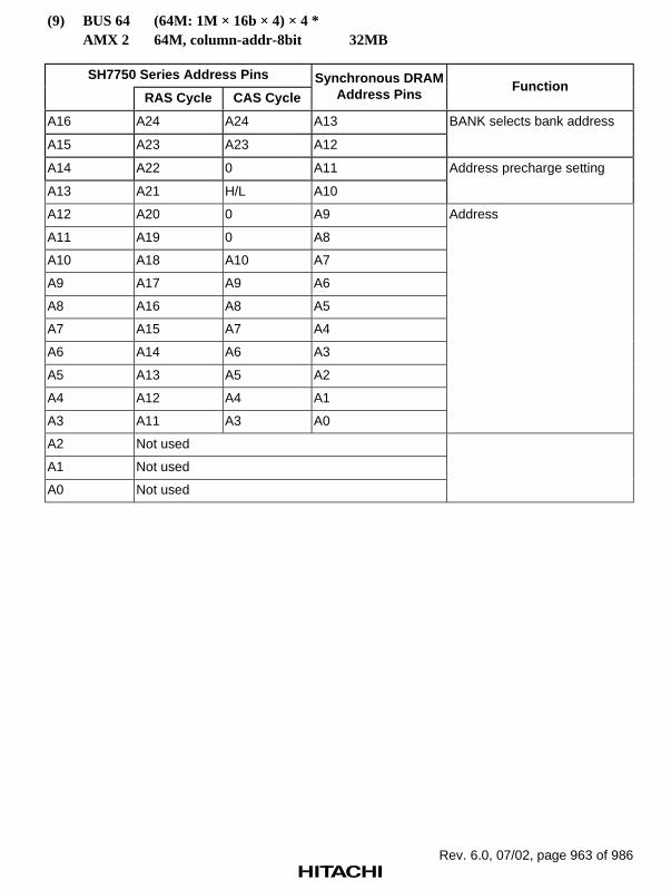
Rev. 6.0, 07/02, page 963 of 986
(9) BUS 64 (64M: 1M × 16b × 4) × 4 *AMX 2 64M, column-addr-8bit 32MB
SH7750 Series Address Pins
RAS Cycle CAS CycleSynchronous DRAM
Address PinsFunction
A16 A24 A24 A13
A15 A23 A23 A12
BANK selects bank address
A14 A22 0 A11
A13 A21 H/L A10
Address precharge setting
A12 A20 0 A9
A11 A19 0 A8
A10 A18 A10 A7
A9 A17 A9 A6
A8 A16 A8 A5
A7 A15 A7 A4
A6 A14 A6 A3
A5 A13 A5 A2
A4 A12 A4 A1
A3 A11 A3 A0
Address
A2 Not used
A1 Not used
A0 Not used

Rev. 6.0, 07/02, page 964 of 986
(10) BUS 32 (64M: 1M × 16b × 4) × 2 *AMX 2 64M, column-addr-8bit 16MB
SH7750 Series Address Pins
RAS Cycle CAS CycleSynchronous DRAM
Address PinsFunction
A16
A15 A23 A23 A13
A14 A22 A22 A12
BANK selects bank address
A13 A21 0 A11
A12 A20 H/L A10
Address precharge setting
A11 A19 0 A9
A10 A18 0 A8
A9 A17 A9 A7
A8 A16 A8 A6
A7 A15 A7 A5
A6 A14 A6 A4
A5 A13 A5 A3
A4 A12 A4 A2
A3 A11 A3 A1
A2 A10 A2 A0
Address
A1 Not used
A0 Not used

Rev. 6.0, 07/02, page 965 of 986
(11) BUS 64 (64M: 2M × 8b × 4) × 8 *(128M: 2M × 16b × 4) × 4
AMX 3 64M, column-addr-9bit 64MB
SH7750 Series Address Pins
RAS Cycle CAS Cycle
Synchronous DRAMAddress Pins
Function
A16 A25 A25 A13
A15 A24 A24 A12
BANK selects bank address
A14 A23 0 A11
A13 A22 H/L A10
Address precharge setting
A12 A21 0 A9
A11 A20 A11 A8
A10 A19 A10 A7
A9 A18 A9 A6
A8 A17 A8 A5
A7 A16 A7 A4
A6 A15 A6 A3
A5 A14 A5 A2
A4 A13 A4 A1
A3 A12 A3 A0
Address
A2 Not used
A1 Not used
A0 Not used

Rev. 6.0, 07/02, page 966 of 986
(12) BUS 32 (64M: 2M × 8b × 4) × 4 *(128M: 2M × 16b × 4) × 2
AMX 3 64M, column-addr-9bit 32MB
SH7750 Series Address Pins
RAS Cycle CAS Cycle
Synchronous DRAMAddress Pins
Function
A16
A15 A24 A24 A13
A14 A23 A23 A12
BANK selects bank address
A13 A22 0 A11
A12 A21 H/L A10
Address precharge setting
A11 A20 0 A9
A10 A19 A10 A8
A9 A18 A9 A7
A8 A17 A8 A6
A7 A16 A7 A5
A6 A15 A6 A4
A5 A14 A5 A3
A4 A13 A4 A2
A3 A12 A3 A1
A2 A11 A2 A0
Address
A1 Not used
A0 Not used

Rev. 6.0, 07/02, page 967 of 986
(13) BUS 64 (64M: 512k × 32b × 4) × 2 *AMX 4 64M, column-addr-8bit 16MB
SH7750 Series Address Pins
RAS Cycle CAS CycleSynchronous DRAM
Address PinsFunction
A15 A23 A23 A12
A14 A22 A22 A11
BANK selects bank address
A13 A21 H/L A10 Address precharge setting
A12 A20 0 A9
A11 A19 0 A8
A10 A18 A10 A7
A9 A17 A9 A6
A8 A16 A8 A5
A7 A15 A7 A4
A6 A14 A6 A3
A5 A13 A5 A2
A4 A12 A4 A1
A3 A11 A3 A0
Address
A2 Not used
A1 Not used
A0 Not used

Rev. 6.0, 07/02, page 968 of 986
(14) BUS 32 (64M: 512k × 32b × 4) × 1 *AMX 4 64M, column-addr-8bit 8MB
SH7750 Series Address Pins
RAS Cycle CAS CycleSynchronous DRAM
Address PinsFunction
A15
A14 A22 A22 A12
A13 A21 A21 A11
BANK selects bank address
A12 A20 H/L A10 Address precharge setting
A11 A19 0 A9
A10 A18 0 A8
A9 A17 A9 A7
A8 A16 A8 A6
A7 A15 A7 A5
A6 A14 A6 A4
A5 A13 A5 A3
A4 A12 A4 A2
A3 A11 A3 A1
A2 A10 A2 A0
Address
A1 Not used
A0 Not used

Rev. 6.0, 07/02, page 969 of 986
(15) BUS 64 (64M: 1M × 32b × 2) × 2 *AMX 5 64M, column-addr-8bit 16MB
SH7750 Series Address Pins
RAS Cycle CAS CycleSynchronous DRAM
Address PinsFunction
A15 A23 A23 A12 BANK selects bank address
A14 A22 0 A11
A13 A21 H/L A10 Address precharge setting
A12 A20 0 A9
A11 A19 0 A8
A10 A18 A10 A7
A9 A17 A9 A6
A8 A16 A8 A5
A7 A15 A7 A4
A6 A14 A6 A3
A5 A13 A5 A2
A4 A12 A4 A1
A3 A11 A3 A0
Address
A2 Not used
A1 Not used
A0 Not used

Rev. 6.0, 07/02, page 970 of 986
(16) BUS 32 (64M: 1M × 32b × 2) × 1 *AMX 5 64M, column-addr-8bit 8MB
SH7750 Series Address Pins
RAS Cycle CAS CycleSynchronous DRAM
Address PinsFunction
A15
A14 A22 A22 A12 BANK selects bank address
A13 A21 0 A11
A12 A20 H/L A10 Address precharge setting
A11 A19 0 A9
A10 A18 0 A8
A9 A17 A9 A7
A8 A16 A8 A6
A7 A15 A7 A5
A6 A14 A6 A4
A5 A13 A5 A3
A4 A12 A4 A2
A3 A11 A3 A1
A2 A10 A2 A0
Address
A1 Not used
A0 Not used

Rev. 6.0, 07/02, page 971 of 986
(17) BUS 64 (128M: 4M × 8b × 4) × 8 (SH7750R only)AMX 6 128M, column-addr-10bit 128MBAMXEXT0
SH7750 Series Address Pins
RAS Cycle CAS CycleSynchronous DRAM
Address PinsFunction
A16 A26 A26 A13
A15 A25 A25 A12
BANK selects bank address
A14 A24 0 A11
A13 A23 H/L A10 Address precharge setting
A12 A22 A12 A9
A11 A21 A11 A8
A10 A20 A10 A7
A9 A19 A9 A6
A8 A18 A8 A5
A7 A17 A7 A4
A6 A16 A6 A3
A5 A15 A5 A2
A4 A14 A4 A1
A3 A13 A3 A0
Address
A2 Not used
A1 Not used
A0 Not used

Rev. 6.0, 07/02, page 972 of 986
(18) BUS 64 (256M: 4M × 16b × 4) × 4 (SH7750R only) *AMX 6 256M, column-addr-9bit 128MBAMXEXT1
SH7750 Series Address Pins
RAS Cycle CAS Cycle
Synchronous DRAMAddress Pins
Function
A17 A26 A26 A14
A16 A25 A25 A13
BANK selects bank address
A15 A24 0 A12
A14 A23 0 A11
A13 A22 H/L A10 Address precharge setting
A12 A21 0 A9
A11 A20 A11 A8
A10 A19 A10 A7
A9 A18 A9 A6
A8 A17 A8 A5
A7 A16 A7 A4
A6 A15 A6 A3
A5 A14 A5 A2
A4 A13 A4 A1
A3 A12 A3 A0
Address
A2 Not used
A1 Not used
A0 Not used

Rev. 6.0, 07/02, page 973 of 986
(19) BUS 32 (128M: 4M ×××× 8b ×××× 4) ×××× 4 (SH7750S and SH7750R only) *AMX 6 column-addr-10bit 64MBAMXEXT 0
SH7750 Series Address Pins
RAS Cycle CAS Cycle
Synchronous DRAMAddress Pins
Function
A15 A25 A25 A13 BANK selects bank address
A14 A24 A24 A12
A13 A23 0 A11 Address precharge setting
A12 A22 H/L A10
A11 A21 A11 A9
A10 A20 A10 A8
A9 A19 A9 A7
A8 A18 A8 A6
A7 A17 A7 A5
A6 A16 A6 A4
A5 A15 A5 A3
A4 A14 A4 A2
A3 A13 A3 A1
A2 A12 A2 A0
Address
A1 Not used
A0 Not used

Rev. 6.0, 07/02, page 974 of 986
(20) BUS 32 (256M: 4M × 16b × 4) × 2 (SH7750S and SH7750R only) *AMX 6 256M, column-addr-9bit 64MBAMXEXT 1
SH7750 Series Address Pins
RAS Cycle CAS Cycle
Synchronous DRAMAddress Pins
Function
A16 A25 A25 A14 BANK selects bank address
A15 A24 A24 A13
A14 A23 0 A12
A13 A22 0 A11
A12 A21 H/L A10 Address precharge setting
A11 A20 0 A9
A10 A19 A10 A8
A9 A18 A9 A7
A8 A17 A8 A6
A7 A16 A7 A5
A6 A15 A6 A4
A5 A14 A5 A3
A4 A13 A4 A2
A3 A12 A3 A1
A2 A11 A2 A0
Address
A1 Not used
A0 Not used

Rev. 6.0, 07/02, page 975 of 986
(21) BUS 64 (16M: 256k × 32b × 2) × 2 *AMX 7 16M, column-addr-8bit 4MB
SH7750 Series Address Pins
RAS Cycle CAS CycleSynchronous DRAM
Address PinsFunction
A13 A21 A21 A10 BANK selects bank address
A12 A20 H/L A9 Address precharge setting
A11 A19 0 A8
A10 A18 A10 A7
A9 A17 A9 A6
A8 A16 A8 A5
A7 A15 A7 A4
A6 A14 A6 A3
A5 A13 A5 A2
A4 A12 A4 A1
A3 A11 A3 A0
Address
A2 Not used
A1 Not used
A0 Not used

Rev. 6.0, 07/02, page 976 of 986
(22) BUS 32 (16M: 256k × 32b × 2) × 1 *AMX 7 16M, column-addr-8bit 2MB
SH7750 Series Address Pins
RAS Cycle CAS CycleSynchronous DRAM
Address PinsFunction
A13
A12 A20 A20 A10 BANK selects bank address
A11 A19 H/L A9 Address precharge setting
A10 A18 0 A8
A9 A17 A9 A7
A8 A16 A8 A6
A7 A15 A7 A5
A6 A14 A6 A4
A5 A13 A5 A3
A4 A12 A4 A2
A3 A11 A3 A1
A2 A10 A2 A0
Address
A1 Not used
A0 Not used
Note: * Example of a synchronous DRAM configuration

Rev. 6.0, 07/02, page 977 of 986
Appendix G Prefetching of Instructions and its Side Effects
The SH7750 series incorporates an on-chip buffer for holding instructions that have been readahead of their execution (prefetching of instructions). Therefore, do not allocate programs tomemory in such a way that instructions are in the last 20 bytes of any memory space. If a programis allocated in such a way, the prefetching of instructions may lead to a bus access for reading aninstruction from beyond the memory space. The following shows a case in which such bus accessis a problem.
PC (Program counter)
Address of instruction for prefetching
Area 0
Area 1
Address
H'03FFFFF8H'03FFFFFAH'03FFFFFCH'03FFFFFEH'04000000H'04000002
ADD R1,R4JMP @R2NOPNOP
.
.
.
.
.
.
Figure G.1 Instruction Prefetch
Figure G.1 depicts a case in which the instruction (ADD) indicated by the program counter and theinstruction at the address H’04000002 are fetched simultaneously. The program is assumed tobranch to a region other than area 1 after the subsequent JMP instruction and delay slot instructionhave been executed.
In this case, a bus access to area 1 (instruction prefetch), which is not visible in the program flow,may occur.
1. Side effects of the prefetching of instructions
a. An external bus access caused by an instruction prefetch may cause malfunctions inexternal devices, such as FIFOs, that are connected to the region accessed.
b. If no device responds to an external bus request that is triggered by an instruction prefetch,execution may hang.
2. Methods of preventing the invalid prefetching of instructions
a. Use an MMU.
b. Do not allocate programs so that they run into the last 20-byte region of any memory space.

Rev. 6.0, 07/02, page 978 of 986
Appendix H Power-On and Power-Off Procedures
• Power-on
Supply the internal power after supplying power to the I/O, PLL, RTC, and CPG.*1
Supply power to VDDQ, VDD-PLL1/2, VDD-RTC, and VDD-CPG simultaneously.
At power-on, the RESET signal is low. Normally, supply power to the I/O, RTC, and CPGbefore (or at the same time as) entering the signal lines (RESET, SCK2, MD0 to MD10,and external clock). If the signal lines are entered first, the LSI may be damaged.
Input high level to SCK2 (MRESET) in compliance with the voltage level of the I/O, PLL,RTC, CPG power supply voltage.
• Power-off
When turning off the power, there are no restrictions for the timing of RESET and SCK2.
Turn off the I/O, PLL, RTC, CPG power supply voltage after (or at the same time as)*1
turning off the internal power supply voltage.
Note however that the internal power supply voltage may exceed the I/O, PLL, RTC, CPGpower supply voltage by a maximum of 0.3 V only when the system is being turned off.
The power supply level must be lowered in compliance with the I/O, PLL, RTC, CPGpower supply voltage.
Note: *1 10 ms or less for the HD6417750R.
• The ratings and procedures for power-on and power-off are given below.
VSSQ = VSS-PLL1 = VSS-PLL2 = VSS-RTC = VSS-CPG = 0 V
The LSI may be damaged if−0.3 V < Vin < VDDQ + 0.3 V−0.3 V < VDD < VDDQ + 0.3 V
are not satisfied when VDDQ = VDD-RTC = VDD-CPG.
2.0 V
1.2 V
GNDton
0 ≤ ton < 10 ms*
toff
0 ≤ toff < 10 ms*
VDD
VDDQPower-on Power-off
Note: * HD6417750R only
Figure H.1 Power-On and Power-Off Procedures

Rev. 6.0, 07/02, page 979 of 986
Appendix I Product Code Lineup
Table I.1 SH7750 Series Product Code Lineup
Abbreviation VoltageOperatingFrequency
OperatingTemperature Mark Code Package
SH7750 1.95 V 200 MHz –20 to 75°C HD6417750BP200M BGA-256
1.8 V 167 MHz –20 to 75°C HD6417750F167 QFP-208
–40 to 85°C HD6417750F167I
1.5 V 128 MHz –20 to 75°C HD6417750VF128
SH7750S 1.95 V 200 MHz –20 to 75°C HD6417750SBP200 BGA-256
–20 to 75°C HD6417750SF200 QFP-208
1.8 V 167 MHz –20 to 75°C HD6417750SF167 QFP-208
–40 to 85°C HD6417750SF167I
1.5 V 133 MHz –20 to 75°C HD6417750SVF133
–30 to 70°C HD6417750SVBT133 CSP-264
SH7750R 1.5 V 240 MHz –20 to 75°C HD6417750RBP240 BGA-256
–20 to 75°C HD6417750RF240 QFP-208
1.5 V 200 MHz –20 to 75°C HD6417750RBP200 BGA-256
–20 to 75°C HD6417750RF200 QFP-208

Rev. 6.0, 07/02, page 980 of 986

Rev. 6.0, 07/02, page 981 of 986
Index
A
Address Space........................................... 64
B
Big endian................................................. 53Bus Arbitration ....................................... 480Bus State Controller................................ 311
Address Multiplexing ......................... 399Areas........................................... 319, 382Burst Access ....................................... 402Burst ROM Interface .......................... 441Byte Control SRAM Interface ............ 473DRAM Interface ................................. 395EDO Mode.......................................... 403Endian................................................. 370I/O card interface ........................ 322, 444IC memory card interface ........... 322, 444Master Mode....................................... 483MPX Interface .................................... 455Partial-Sharing Master Mode.............. 485PCMCIA Interface.............................. 444PCMCIA Support ............................... 322RAS Down Mode ............................... 404Refresh Timing ................................... 409Refreshing........................................... 431Slave Mode ......................................... 484SRAM Interface.................................. 387Synchronous DRAM Interface ........... 413Wait State Control .............................. 401Waits between Access Cycles............. 478
C
Caches....................................................... 95Address Array............. 112, 114, 117, 119cache fill ............................................. 108Data Array .................. 113, 115, 118, 120IC Index Mode.................................... 111Instruction Cache .......................... 95, 108OC Index Mode .................................. 107
Operand Cache................................ 95, 99prefetch ...............................................122Prefetch Operation ..............................108RAM Mode .........................................106Store Queues .......................................122Tag .............................................. 102, 110U bit ....................................................102V bit ............................................ 102, 110Write-Back Buffer...............................105Write-Through Buffer .........................105
Clock Oscillation Circuits .......................247Bus Clock Division Ratio....................258Changing the Frequency .....................257Clock Operating Modes ......................253PLL Circuit .........................................257
clock pulse generator ..............................247Control Registers ................................ 42, 49
DBR ......................................................50Debug base register ...............................50GBR ......................................................50Global base register...............................50Saved general register 15 ......................50Saved program counter .........................50Saved status register..............................50SGR.......................................................50SPC .......................................................50SR..........................................................49SSR .......................................................50Status register........................................49VBR ......................................................50Vector base register...............................50
D
Data Format ..............................................53Direct Memory Access Controller ..........489
Address Modes....................................519Burst Mode..........................................523Bus Modes ..........................................522Channel Priorities................................515Cycle Steal Mode ................................522

Rev. 6.0, 07/02, page 982 of 986
DMA Transfer .................................... 518DMA Transfer Requests ..................... 512Dual Address Mode ............................ 520Ending DMA Transfer ........................ 541Fixed Mode......................................... 515On-Demand Data Transfer Mode ....... 545Round Robin Mode............................. 515Single Address Mode.......................... 519
E
effective address ..................................... 175Exceptions .............................................. 127
Address Error.............................. 146, 147Exception Types ................................. 130FPU exception ............................ 154, 169General Exceptions ............................. 141General FPU Disable Exception ......... 151General illegal instruction................... 169General Illegal Instruction Exception . 149Initial Page Write Exception............... 143Instruction TLB Protection Violation
Exception ........................................ 145Slot FPU Disable Exception ............... 152slot illegal instruction exception ......... 169Slot Illegal Instruction Exception ....... 150TLB Miss Exception................... 141, 142TLB Multiple-Hit Exception....... 139, 140TLB Protection Violation Exception .. 144Unconditional Trap............................. 148User Breakpoint Trap ......................... 153
External Memory Space Map ................. 320
F
Floating-Point Registers ............. 43, 47, 165Floating-Point Unit ................................. 161
Denormalized Numbers ...................... 164Floating-Point Format......................... 161Geometric Operation Instructions....... 170NaN............................................. 163, 164Non-Numbers ..................................... 163Pair Single-Precision Data Transfer.... 172
G
General Registers ................................ 42, 45Graphics Support Functions....................170
H
Hitachi User Debug Interface..................799TAP Control........................................810
I
I/O Ports..................................................731Instruction Set ................................. 173, 179
Arithmetic Operation Instructions.......182Branch instructions ..................... 186, 214Data transfer instructions ....................211Double-precision floating-point
instructions......................................217Fixed-point arithmetic instructions .....212Fixed-Point Transfer Instructions........180Floating-Point Control Instructions.....190Floating-Point Double-Precision
Instructions......................................190Floating-Point Graphics Acceleration
Instructions......................................191Floating-Point Single-Precision
Instructions......................................189FPU system control instructions .........218Graphics acceleration instructions ......218Logic Operation Instructions...............184Shift instructions ......................... 185, 214Single-precision floating-point
instructions......................................216System control instructions ......... 187, 215
Interrupt Controller .................................751Interrupt Priority .................................759On-Chip Peripheral Module Interrupts757
Interrupts .................................................155ATI......................................................289BRI......................................................697ERI ...................................... 651, 697, 724IRL Interrupts.............................. 156, 755NMI.....................................................155NMI Interrupt......................................754Peripheral Module Interrupts ..............157

Rev. 6.0, 07/02, page 983 of 986
PRI...................................................... 289RXI ..................................... 651, 697, 724TEI...................................................... 651TICPI .................................................. 309TUNI................................................... 309TXI ..................................... 651, 697, 724
L
Little endian.............................................. 53
M
Memory Management Unit....................... 57Address Array................................. 88, 90Address Space Identifier ....................... 70Address Translation .............................. 69Address Translation Method................. 75ASID..................................................... 70Avoiding Synonym Problems............... 80Data Array ...................................... 89, 92External memory space................... 64, 67ITLB ..................................................... 75LDTLB ................................................. 78MMU Exceptions.................................. 81MMU Functions.................................... 78Physical address space .................... 58, 64time sharing system .............................. 57TLB................................................. 57, 71UTLB.................................................... 71Virtual address space ...................... 58, 68virtual memory system.......................... 57
P
Pipelining................................................ 193Execution Cycles ........................ 204, 211Parallel-Executability.......................... 200Pipeline Stalling.................................. 204
Power-Down Modes ............................... 221Clock Pause Function ......................... 232Deep Sleep Mode................................ 230Exit from Standby Mode..................... 232Hardware Standby Mode .................... 235High Impedance Control..................... 226Module Standby Function................... 233
Pull-Up Control...................................226Sleep Mode .........................................230
Programming Model .................................41Banks.....................................................42Data Formats .........................................41Privileged Mode....................................42
R
Realtime Clock........................................267Alarm Function ...................................288Crystal Oscillator Circuit ....................289CUI......................................................289Time Setting........................................285
RegistersBAMRA..............................................778BAMRB ..............................................781BARA .................................................777BARB..................................................781BASRA ...............................................778BASRB ...............................................781BBRA..................................................779BBRB..................................................783BCR1 ..................................................326BCR2 ..................................................335BDRB..................................................781BRCR..................................................783CCR ......................................................97CHCR..................................................499DAR ....................................................497DMAOR..............................................507DMATCR ...........................................498EXPEVT .............................................128FPSCR.................................................167FPUL...................................................168FRQCR ...............................................254GPIOIC ...............................................745ICR......................................................762INTEVT ..............................................128IPR ......................................................761MCR....................................................352MMUCR ...............................................61PCR.....................................................359PCTRA................................................742

Rev. 6.0, 07/02, page 984 of 986
PCTRB ............................................... 744PDTRA ............................................... 743PDTRB ............................................... 745PTEH .................................................... 61QACR0 ................................................. 97R64CNT.............................................. 271RCR1 .................................................. 279RCR2 .................................................. 281RDAYAR ........................................... 278RDAYCNT......................................... 274RFCR.................................................. 369RHRAR .............................................. 277RHRCNT ............................................ 272RMINAR ............................................ 276RMINCNT.......................................... 272RMONAR........................................... 279RMONCNT ........................................ 274RSECAR............................................. 276RSECCNT .......................................... 271RTCNT ............................................... 367RTCOR............................................... 368RTCSR................................................ 364RWKAR ............................................. 277RWKCNT........................................... 273RYRCNT ............................................ 275SAR .................................................... 496SCBRR1 ............................................. 613SCBRR2 ............................................. 674SCFCR2.............................................. 675SCFDR2.............................................. 678SCFRDR2........................................... 662SCFSR2 .............................................. 668SCFTDR2 ........................................... 663SCLSR2 .............................................. 684SCRDR1 ............................................. 597SCRSR1.............................................. 597SCRSR2.............................................. 661SCSCMR1 .......................................... 706SCSCR1...................................... 601, 708SCSCR2.............................................. 665SCSMR1..................................... 599, 707SCSMR2............................................. 663SCSPTR1.................................... 609, 746
SCSPTR2 .................................... 679, 748SCSSR1....................................... 605, 709SCTDR1..............................................598SCTSR1 ..............................................598SCTSR2 ..............................................662SDBPR................................................805SDDR..................................................805SDIR ...................................................803SDMR .................................................362STBCR................................................224STBCR2..............................................227TCNT..................................................298TCOR..................................................298TCPR2 ................................................303TCR.....................................................299TEA.......................................................61TOCR..................................................295TRA ....................................................128TSTR...................................................296TTB.......................................................61WCR1 .................................................340WCR2 .................................................343WCR3 .................................................351WTCNT ..............................................260WTCSR...............................................261
Resets ......................................................136H-UDI Reset ............................... 138, 811Manual Reset ......................................137Power-On Reset ..................................136
Rounding.................................................168
S
Serial Communication Interface .............593Asynchronous mode.................... 621, 623Bit Rate ...............................................613Break...................................................652Framing error .............................. 632, 652Multiprocessor Communication Function
........................................................634Overrun error .............................. 632, 652Parity error .................................. 632, 652Synchronous mode...................... 621, 642

Rev. 6.0, 07/02, page 985 of 986
Serial Communication Interface with FIFO............................................................ 657Asynchronous Mode........................... 685Break................................................... 698
Smart Card Interface............................... 703bit rate ................................................. 715
System Registers................................. 42, 50Floating-point status/control register .... 51FPSCR .................................................. 51MACH .................................................. 50MACL................................................... 50Multiply-and-accumulate register high. 50Multiply-and-accumulate register low.. 50PC ......................................................... 50PR ......................................................... 50Procedure register ................................. 50Program counter.................................... 50
T
Timer Unit...............................................291Auto-Reload Count Operation ............305Input Capture Function .......................307TCNT Count Timing...........................306
U
User Break Controller .............................773Instruction Access Cycle Break ..........788Operand Access Cycle Break..............789User Break Debug Support Function ..793User Break Operation Sequence .........787
W
Watchdog Timer ............................. 247, 259Interval Timer Mode ...........................265Watchdog Timer Mode .......................264

Rev. 6.0, 07/02, page 986 of 986

SH7750 Series Hardware Manual
Publication Date: 1st Edition, June 19986th Edition, July 2002
Published by: Business Operation DivisionSemiconductor & Integrated CircuitsHitachi, Ltd.
Edited by: Technical Documentation GroupHitachi Kodaira Semiconductor Co., Ltd.
Copyright © Hitachi, Ltd., 1998. All rights reserved. Printed in Japan.


