SH77P1651 APPLICATION NOTE 1 Introduction The SH77P1651 is an 8051 compatible micro-controller with a redesigned CPU of high efficiency and high performance, with 16K-Byte OTP ROM. The Evaluation Version named SH77V1651, used 16K RAM instead of OTP ROM allows multiple times downloading and on-line debugging. Make sure the power is always on when using EV, or the code in RAM will lost. Downloading SH77P1651 was realized by using ProWriter and Pro03A. Downloading and debugging SH77V1651 was realized by JET51. The Sinowealth 8051 JET51 Driver is intended to provide the product development engineer with a complete microcontroller design tool set for Sinowealth 8 bit microcontrollers. Software control of the JET51 Driver is advanced by the Keil μ vision Integrated Development Environment via a JTAG interface, which allows editing, building, downloading and source debugging from a single environment. 1.1 EV Demo Board The EV Demo board is provided to assist the user to explore the SH77V1651. Figure1 shows the front view of the board. Figure1: The SH77V1651 Demo Board A. Power LED B. External power supply interface 1(VDD/GND) Apply external power at the VDD pin directly, where the user determines the voltage level. C. Current Test Interface Disconnect the first pin on left from the other pins and power supply connect with any of the three pins left when testing the power consume of the IC. D. Emulator Interface (JTAG Interface) Communicate with the JET51 driver via a 10-pin cable. The power supply can also be provided by VDD
Transcript
SH77P1651 APPLICATION NOTE
1 Introduction
The SH77P1651 is an 8051 compatible micro-controller with a redesigned CPU of high efficiency and
high performance, with 16K-Byte OTP ROM. The Evaluation Version named SH77V1651, used 16K
RAM instead of OTP ROM allows multiple times downloading and on-line debugging. Make sure the
power is always on when using EV, or the code in RAM will lost.
Downloading SH77P1651 was realized by using ProWriter and Pro03A.
Downloading and debugging SH77V1651 was realized by JET51. The Sinowealth 8051 JET51 Driver is
intended to provide the product development engineer with a complete microcontroller design tool set for
Sinowealth 8 bit microcontrollers. Software control of the JET51 Driver is advanced by the Keil µ vision
Integrated Development Environment via a JTAG interface, which allows editing, building, downloading
and source debugging from a single environment.
1.1 EV Demo Board
The EV Demo board is provided to assist the user to explore the SH77V1651. Figure1 shows the front
view of the board.
Figure1: The SH77V1651 Demo Board
A. Power LED
B. External power supply interface 1(VDD/GND)
Apply external power at the VDD pin directly, where the user determines the voltage level.
C. Current Test Interface
Disconnect the first pin on left from the other pins and power supply connect with any of the three pins
left when testing the power consume of the IC.
D. Emulator Interface (JTAG Interface)
Communicate with the JET51 driver via a 10-pin cable. The power supply can also be provided by VDD
wire of the emulator interface when the JET51 driver is connected to PC.
E. Pin Reset Push Key.
F. Capacitor selection for capacitive LCD .
Connect J2, J7, J11, J10, J9 when using capacitive LCD, disconnect them when using resistor LCD
when the corresponding pin used as IO.
G. Reset pin connector
When the jumper J15 connects as the Figure1, Pin 44 is used as reset pin which is set by OP_RST.
Otherwise, Pin 44 is used as P5.5.
H. External power supply interface 2.
The 5V power supply generated fixed 3.3V by the regulator which was used as SH77V1651 power
supply.
I. JTAG Mode enabled Key.
Push four keys to ON when using JTAG to debug.
J Normal Mode enabled Key.
After downloading in SH77V1651, press this key and unplug JTAG, the code will run in normal mode
after 30s.
K. COB48 or SOCKET placement.
L. OTP program (Reserved).
Note:
1. Switch to Normal Mode.
Download to SH77V1651 by Keil, keep external power supply, press NORMAL_EN key and unplug
JTAG(or push the JTAG mode enable key to OFF), wait for 30s.
2. JTAG shared with LCD SEG18~21.
When using SEG18~21 in JTAG mode, the JTAG will affect the LCD. So do not use SEG18~21 in JTAG
mode. If use SEG18~21, switch to normal mode.
3. COB48 or SOCKET placement.
Make sure the pins are connected correctly.
1.2 Package
TQFP48
1.3 EV JTAG Interface.
The SH77V1651 can debug on line by JTAG interface.
The JTAG emulator Communicates with the JET51 driver via a 10-pin cable. The power supply can also
be provided by VDD wire of the emulator interface when the JET51 driver is connected to PC.
1VDD
GND
TCK
TMS
TDI
TDO
GND
User board implements all of the function by JET51, the power supply of the user board can choose
external power supply interface or emulation interface.
2 Using Target Board
2.1 Installing Software for JET51 Driver
Follow the steps below to install software for JET51 driver:
1) Install Keil uVision2 (Version2.38 or more) or uVision3 or uVision4
2) Install JET51_Keil_Vxxx.exe (Vxxx denotes version), the device library for Sinowealth 8-bit
microcontrollers, to the Keil C directory.(example: C:\Keil\UV2)
3) Connect the JET51 driver to the PC via a USB cable. The red power LED and green USB LED will turn
on if the installation is successful.
2.2 Installing Hardware for Target Board
Set up the target board as follows:
1) Connect the flat cable from the SH77P1651 target board to the JET51 driver via JTAG interface (VDD,
TCK, TDI, TMS, TDO and GND).
USB
PWR
USBTCK
TDI
TMS
TDO
GND
VDD
GND 10
PINs
TCK
TDI
TMS
TDO
GND
VDD
GND10
PINs
JET51
SH77P1651
Target Board
2) The JTAG pins of the SH77P1651 cannot be used as LCD Segment when downloading and
debugging the application code. To communicate successfully with the emulator, make sure the JTAG
pins are connected with no loads.
JET 51
To Application
CircuitJumper
TDI
TMS
TDO
GND
VDD
TCK
SH77P1651
2.3 Creating a Project
The following steps describe how to create a new project. The source file – aa.asm located in ...\user
directory.
Step1: Launch Keil uVision, Select ProjectNew
Project。
Step2: Explore to the source file directory \user. Type in Prj01 for the project name. Click the Save button to save the project.
Step3: Select ”Sino Wealth 8051 Devices”
from pull down list, Click“OK”button.
Step 4: Select the device SH77V1651 and click the OK button.
Step5: Click the NO button to close the dialog. An empty project has been created.
Step6:
Select Project-->Options for
Target "Target1" to pop up
the “Options for Target”
dialog.
Step7:
Click the Debug
tag. Check Use
option and select
“Sino Wealth 8051
JET Driver”from
the pull down
list.
Step8:
Click the
Utilities
tag.Check the Use
Target Driver for
Flash Programming
option and select
“Sino Wealth 8051
JET Driver” from
the pull down
list.
Step9:
Expand the Target1 folder.
Right click the Source
Group1 folder and select
the “Add Files to
Group/Source Group1”item.
The “Add Files to Group”
dialog will come up.
Explore to the destination
directory \user. Select the
source file aa.asm. Click
the Add button to add the
file.
Step10:
Double click aa.asm. The
file will open in the
client area of Keil
uVision.
2.4 Building a Project and Downloading to the Flash Memory
2.4.1 Building a Project
Select Project->Build target or click the corresponding button to build the source files. If no compilation
error and linking error are found, OBJ and HEX files will generate. The generated files can be found in
the directory \user.
2.4 Downloading to the Flash Program Memory
2.4.1 Setting for Downloading
Before downloading the code, some options, including programming device, device’s code option and
power supply source, must be determined. Since the options will save automatically each time you set
them, this step can be skipped once you did before.
Step1:
Select Project-->Option for
Target 'Target 1' or click
the corresponding button
directly.
Step2:
Click the Utilities
tag.Click the Setting
button and the
“Setting” dialog will
pop up. Select
“SH77V1651”
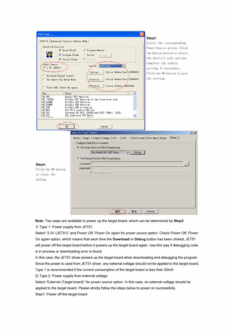
Step3:
Select the corresponding
Power Source option. Click
the Option button to select
the device’s code options.
Complete the others
setting if necessary.
Click the OK button to save
the setting.
Step4:
Click the OK button
to close the
dialog.
Note: Two ways are available to power up the target board, which can be determined by Step3.
1) Type 1: Power supply from JET51
Select “3.3V (JET51)” and Power Off, Power On again for power source option. Check Power Off, Power
On again option, which means that each time the Download or Debug button has been clicked, JET51
will power off the target board before it powers up the target board again. Use this way if debugging code
is in process or downloading error is found.
In this case, the JET51 driver powers up the target board when downloading and debugging the program.
Since the power is used from JET51 driver, any external voltage should not be applied to the target board.
Type 1 is recommended if the current consumption of the target board is less than 20mA.
2) Type 2: Power supply from external voltage.
Select “External (Target board)” for power source option. In this case, an external voltage should be
applied to the target board. Please strictly follow the steps below to power on successfully.
Step1: Power off the target board
Step2: Connect JET51 driver with the target board
Step3: Connect the USB cable from JET51 driver to PC. The red power LED and green USB LED will
turn on if the connection is successful.
Step4: Apply external voltage to the target board.
Once the target board has been set up as previously described, you can download and debug the
application program repeatedly without powering off and reconnecting the target board again
.
2.4.2 Downloading to the Flash Memory
Select Flash-->Download
or click the Download
button to download
user’s code.
Success
information for
downloading.
2.5 Debugging Source Code(for EV)
Select the menu item Debug->Start/Stop Debug Session or click the corresponding button to enter the
debugging mode of the device. Once the device enters into its debugging mode, a yellow arrow will point
to 0000H location and the SP register in left pane read 07H. The feature of in circuit debugging enable
the designer to develop and debug source code by setting breakpoints, single stepping and watching
variables, and CPU status and peripheral registers. Running at full speed
enables testing hardware and applications in real time.
Note:
1) The instruction at the breakpoint location has been executed when the device breaks.
2) The next statement of ACALL or LCALL statement will execute when step over these statements.
3) The emulator supports total 7 breakpoints. If more than 7 breakpoints have been set, the last 7
breakpoints work and the others are ignored.
4) To run the device in offline mode, power off the device and disconnect it from JET51 driver.
5) Apply external voltage to the target board again, and the device will operate under offline mode.
3 Design Tips
3.1 CPU
The SH77P1651 is an 8051 compatible microcontroller with an enhancing CPU core. The CPU function
is intensified in the following aspects:
3.1.1 The SH77P1651 CPU machine cycle is the same as its oscillator clock, while the traditional 8051
CPU machine cycle is composed of 12 oscillator clock cycles. When the same oscillator frequency is
selected, the SH77P1651 devices run almost 10 times faster than the traditional 8051 devices. See the
SH77P1651 datasheet for the detail instruction execution cycles.
3.1.2 The device has implemented enhanced multiplication and division instructions, where 16bit×8bit
and 16bit÷8bit.
3.1.3 The device has implemented dual data pointers (DPTR and DPTR1). It is convenient for the user to
branch table and move data using two data pointers.
3.1.4 The device has external RAM BANK, indirect instruction MOVX @Ri, A or MOVX A, @Ri to access
external RAM above 256 bytes.
3.1.5 The device resets when a required low pulse is applied on the RESET pin, while the traditional
8051 devices require a high pulse to reset.
3.1.6 The system clock can be configured by CLKCON(0B2H).The default pre-scalar is 1/12, user can
configure to 1/2, 1/4 or 1 by changing the value of CLKCON.
3.1.7 The pre-scalar is not available to high frequency system clock.
3.1.8 Please check the instruction cycle before get the exact delay time.
3.2 OTP ROM
The SH77P1651 uses 16K OTP ROM to save code, and can download only once. The user can use
SH77V1651 debug firstly, then use SH77P1651 downloading.
3.3.2 The address of internal RAM is 0~0FFH, the128 bytes of RAM (addresses 00H to 7FH) are directly
and indirectly addressable. address 80H to 0FFH are only indirectly addressable. The Special Function
Registers, SFRs, (addresses 80H to FFH) are directly addressable only.
3.3.3 The external RAM is addressed from 00H~11DH. Traditional 8051 only can access external RAM
from 00H~FFH while SH79FXX provides XPAGE register to represent the high 8 bytes address of RAM
to access external RAM above 256 bytes only with MOVX A, @Ri instruction.
3.3.4 The LCD RAM can be used as normal data RAM when LCD function is disabled.
3.4 System Clock 3.4.1 SH77P1651 has three oscillator types: 32.768kHz crystal oscillator, internal RC (4MHz) and
internal RC (32kHz). SH77P1651 can select low or high frequency clock as system clock. The default system clock is low frequency clock (32.768kHz crystal oscillator or internal 32kHz RC). Altering the value of CLKCON can switch the system clock between low and high frequency.
3.4.2 CLKS[1:0] is available to high frequency(4M) only.
3.4.3 When power on reset, the default value of CLKS[1:0] is 11,altering the value of CLKS[1:0] can
configure the pre-scalar to 1/4, 1/2 or 1.
3.4.4 Once the device is powered up, the 32K_SPDUP bit in the CLKCON register would be set by
hardware automatically to reduce the start-up time of 32KHz crystal oscillator. Since the enhanced 32K
oscillating circuitry consumes 1~2uA more current, clear the 32K_SPDUP bit by software to disable the
supplementary circuitry to save current consumption when the CPU starts to execute instructions. To
decrease the delay following wake event to leave Power-down mode, set the 32K_SPDUP bit by
software to enable the speeding up circuit of 32K oscillation before entering Power-down mode. Clear
the control bit to close the speeding up circuitry to save power consumption when Power-down mode has
exited.
3.4.5 If system clock selects 32.768kHz crystal or the internal 32kHz RC, power-Down mode will stop all
the clocks including CPU and peripherals. If system clock selects internal 4MHz RC, power-down mode will stop all the clocks including CPU and peripherals (except 32kHz / 32.768KHz used to LCD and timer3). So switch the system clock to high frequency if Timer3 or LCD is required to work in power-down
mode.
3.5 Interrupts
3.5.1 When the I/O pin is used as the external interrupt input, only the pin configured as input can cause
the interrupt to occur. Setting the EXx (x=0/1) bits will turn on the internal pull-up resistors automatically.
The pull-up resistance is about 30 kΩ. When the I/O pin outputs low just before it is configured as the
external interrupt input and low-level trigger is selected at the same time, an interrupt request would
happen in respect that a low level, remaining on the pin for the capacitance loads and slow internal
pulling up, was detected by the built-in low level detecting circuitry. After turning on theinternal pull-up
resistor, a delay, for example 5 NOP instructions, is recommended to eliminate the undetermined state
before enabling the interrupt.
3.5.2 Before switching from the external interrupt input to a second function of the I/O pin, clear the EXx
(x=0/1) bits to turn off the external interrupts, or the execution would vector to the external interrupt
service routine if the requirements of the interrupt is met for changing the port function.
3.5.3 The following steps illustrate how to configure an I/O pin to an external interrupt input (INT0/P0.4 is
taken for example):
1) Clear the P0CR.4 bit to select input mode, and set the P0PCR.4 bit to turn on the internal pull up
resistor
2) 5 NOP statements
3) Configure the IT0 bit of the TCON register to select the trigger mode, and clear the IE0 bit to remove
the possible generated interrupt flag.
4) Set the EX0 bit in the IEN0 register to enable the external interrupt 0, and set the EA bit to enable the
global interrupt.
3.5.4 Follow the steps below to wake up IDLE and Power-down mode correctly (INT0/P0.4 is taken for
example):
1) Configure the P0.4 pin as described above. Once, according to the selected trigger mode, the CPU
detected a falling edge or a low level, it will exit from IDLE and Power-down mode.
2) The execution would resume from the interrupt service routine of the external interrupt 0 immediately
after the waking-up of the CPU. Return to the main program by RETI instruction
3) The instructions after the 3 NOP instructions will execute later.
3.6 Timer3
3.6.1 Timer3 is a 16-bit auto-reload timer. It is implemented as a 16-bit register accessed as two
cascaded Data Registers: TH3 and TL3. When reading from TH3 and TL3, they are used as timer
counter register.
3.6.2 Read or write operation to TH3 and TL3 should follow these steps:
Write operation: Low nibble first, High nibble to update the counter
Read operation: High nibble first, Low nibble followed.
3.6.3. Timer3 can work in Power Down mode, the T3CLKS[1:0] should be set 01 or 10.
3.7 LCD
3.7.1 The SH77P1651 build in 4COM×30SEG or 5COM×29SEG LCD.
3.7.2 SH77P1651/SH77P1652 provides three different ways of LCD driver: resistor LCD driver, capacitor
bias voltage LCD driver and capacitor regulator LCD driver:
(1) The performance of resistor LCD driver which consume the most power of the three types and need
no external circuit will get worse when the voltage is lower.
(2) The capacitor regulator LCD which need PUMP circuit won’t get worse when the voltage is lower.
(3) The capacitor bias voltage LCD which consume the least power of the three types and need PUMP
circuit will get worse when the voltage is lower.
3.7.3 When selecting the capacitor bias voltage or capacitor regulator LCD, the PUMPON bit of LCDCON
should be set to 1.
3.7.4 When using LCD drive, make sure the COM/SEG pin is correctly connected and the corresponding
bit of LCD RAM is set to 1 according to SPEC.
3.7.5 It’s recommended to use the LCD segment function when debugging LCD in JTAG mode in
SH77V1651, for the JTAG will affect the LCD wave when debugging. Make sure in normal mode when
verifying SEG18~SEG21 function.
3.7.6 The LCD wave will be abnormal if the function of P3.7 is configured of VREF and SEG24
simultaneously.
3.8 UART
3.8.1 The TXD/RXD pin may be shared as I/O function, the RXD pin will be configured as input-pull up
automatically when REN bit is set as 1. But the TXD pin is used as UART function only when users write
data to SBUF register, and goes back to I/O function automatically when UART transmission is over. So
it is recommend to configure the TXD pin as output high level before UART transmission which can avoid
that the receiver get error information.
3.8.2 Both Timer2 and Timer4 can be selected as baud rate clock source of UART controlled by TCLK
and RCLK bits. If set TCLK or RCLK bit as logic 0, Timer1 acts as the baud rate clock source, if set TCLK
or RCLK bit as logic 1, Timer2 acts as the baud rate clock source. This shows that UART can use
deferent baud rate in transmission and reception.
3.8.3 The maximum tolerance of UART reception baud rate is ±4%
3.9 REM
3.9.1 The cycle and duty of infrared emission carrier is decided by the cycle and duty of PWM1.
3.9.2 The infrared emission should configure the following parameters:
(1) Set PWM1SS to 1.
(2) Set PWM1P, PWM1D to 1.
(3) Set REMSW to 1.
(4) Set REMNUMH, REMNUML.
(5) Set PWM1EN to 1, turn on infrared emission.
Note: when using REM, the REMSW is forbidden to clear to 0, for the P5.4 will switch to PWM1 and the
sinking current will burn out the chip.
3.9.3 Stop the infrared emission should according to the following steps:
(1) Both of the value of REMNUMH and REMNUML are 0.(see SPEC for the details )
(2) Clear the PWM1EN to 0.
Then the infrared emission stops, and the port of REM is high-z state.
Configure corresponding levels of CODE OPTION to achieve different emission power.