Scuola di Ingegneria Industriale e dell’Informazione Dipartimento di Elettronica, Informazione e Bioingegneria Short-reach optical fiber links for PCI Express interconnections Relatore: Prof. Pierpaolo BOFFI Correlatore: Ing. Alberto GATTO Tesi di Laurea Magistrale di: Francesco CORAPI Matr. 833113 Anno Accademico 2015-2016
Transcript
Scuola di Ingegneria Industriale e dell’InformazioneDipartimento di Elettronica, Informazione e Bioingegneria
Short-reach optical fiber links for PCI Expressinterconnections
Relatore: Prof. Pierpaolo BOFFICorrelatore: Ing. Alberto GATTO
Tesi di Laurea Magistrale di:Francesco CORAPI Matr. 833113
3.1 Experimental setup for the physical analysis. . . . . . . . . . . 293.2 Experimental setup for BER measurements. . . . . . . . . . . 303.3 The convolution of two delta functions separated by DJ and a
Gaussian RJ distribution of width σ. . . . . . . . . . . . . . . 333.4 Relation between eye diagram and jitter distribution. . . . . . 343.5 Bathtub plot example. . . . . . . . . . . . . . . . . . . . . . . 353.6 PCI Express Waveform Mask Specifications. . . . . . . . . . . 363.7 Signal view on the oscilloscope in caso of GEN1 PCIe trans-
eye diagram, (b)TJ@BER: bathtub . . . . . . . . . . . . . . . 383.9 Characterization of the BER at different distances for GEN1. . 393.10 Physical characterization of the GEN2 signal: (a) Mask Hits:
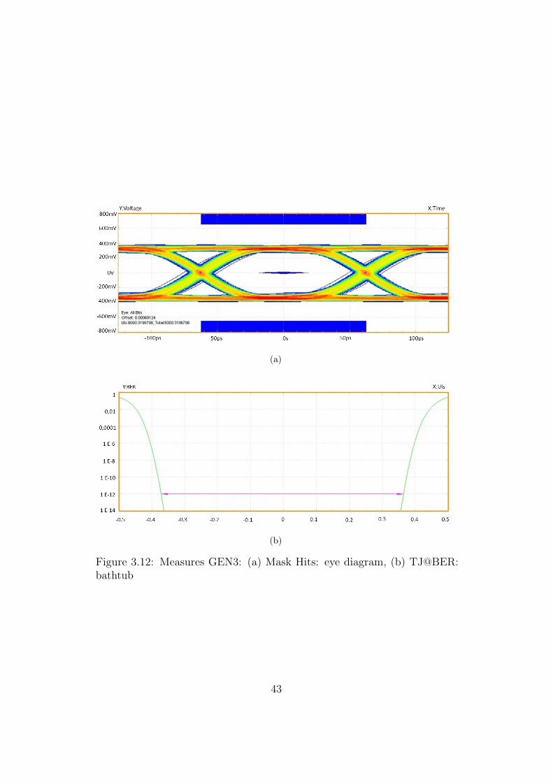
eye diagram, (b) TJ@BER: bathtub . . . . . . . . . . . . . . . 403.11 Characterization of the BER at different distances for GEN2. . 413.12 Measures GEN3: (a) Mask Hits: eye diagram, (b) TJ@BER:
bathtub . . . . . . . . . . . . . . . . . . . . . . . . . . . . . . 433.13 Characterization of the BER at different distances for GEN3. . 44
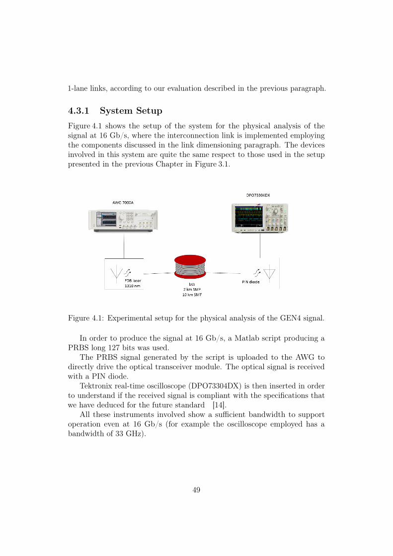
4.1 Experimental setup for the physical analysis of the GEN4 signal. 49
iii
4.2 GEN4 signal characterization in btb operation mode: (a) eyediagram with the mask (b) bathtub curve. . . . . . . . . . . . 50
4.3 GEN4 signal characterization after 2 km of SMF link: (a) eyediagram with the mask (b) bathtub curve. . . . . . . . . . . . 51
4.4 GEN4 signal characterization after 10 km of SMF link: (a) eyediagram with the mask (b) histogram of the jitter. . . . . . . . 52
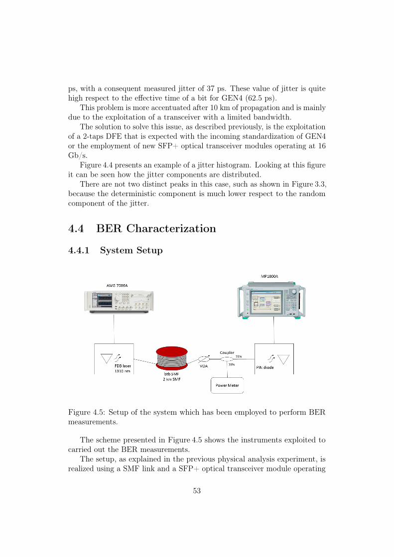
4.5 Setup of the system which has been employed to perform BERmeasurements. . . . . . . . . . . . . . . . . . . . . . . . . . . . 53
4.6 BER measure in back-to-back operation mode and with a linkof 2 km and 10 km. . . . . . . . . . . . . . . . . . . . . . . . . 55
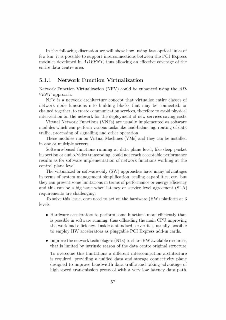
5.1 On the left a standard cluster configuration while on the righta full PCIe fabric connecting a mini-cluster of servers. . . . . . 59
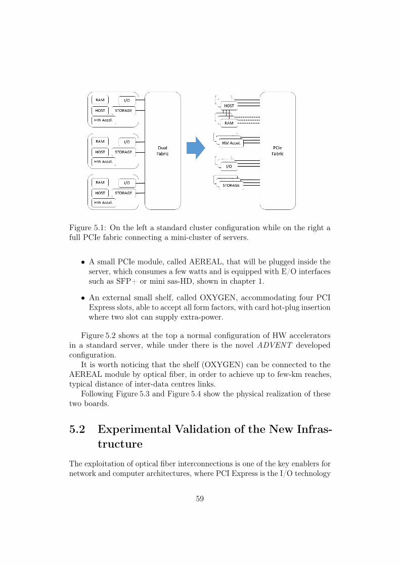
5.2 TOP: Hardware accelerators in a standard server. BOTTOM:PCIe bus extension to get more HW accelerators. . . . . . . . 60
5.3 AEREAL cards inserted in a standard PC motherboard. . . . 605.4 Some HW accelerators plugged on the OXYGEN board. . . . 615.5 Setup of the experiment for the physical analysis of the signal
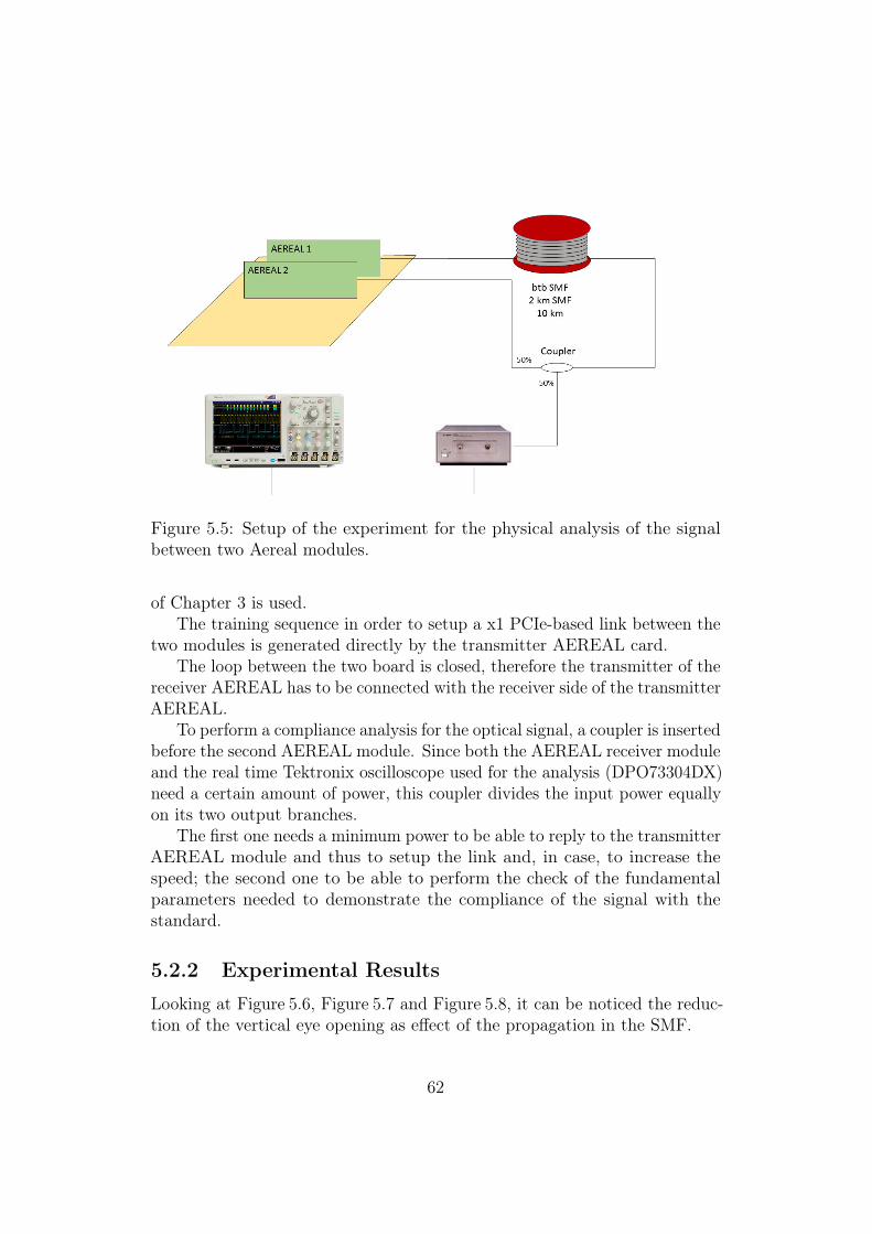
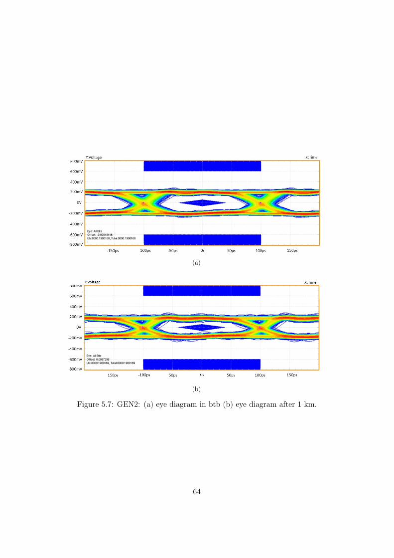
between two Aereal modules. . . . . . . . . . . . . . . . . . . . 625.6 GEN1: (a) eye diagram in btb (b) eye diagram after 1 km. . . 635.7 GEN2: (a) eye diagram in btb (b) eye diagram after 1 km. . . 645.8 GEN3: (a) eye diagram in btb (b) eye diagram after 1 km (c)
eye diagram after 10 km . . . . . . . . . . . . . . . . . . . . . 655.9 GEN1 : (a) bathtub curve in btb (b) bathtub curve after 1 km. 665.10 GEN2: (a) bathtub curve in btb (b) bathtub curve after 1 km. 675.11 GEN3: (a) bathtub curve in btb (b) bathtub curve after 1 km
4.1 Maximum distance reachable in GEN4 expressed in km . . . . 48
v
Abstract
Within the last years, data traffic managed by data centres has grownexponentially due to the success of the internet of things andeverything-as-a-service paradigms, expecting a huge increase in
the near future, thus pushing traditional architectures up to the limit.Peripheral Component Interface Express (PCIe) protocol combined to
optical fiber interconnections are the key elements to enable the developmentof new intra-data centre infrastructures.
In this thesis new network architectures based on the PCI Express forlow power heterogeneous computing systems protocol will be presented, thusimproving performance, efficiency, reliability, scalability and functional charac-teristics of today server clusters in data centre like environment by exploitingthe capability of fiber optic communications.
This disruptive scenario developed within the Advanced Virtualizationfor Enabling Network Technology and Applications (ADVENT ) project isbased on a unique PCIe fabric and assures convergent, storage/analyticfunctionalities mapped to a global shared memory.
The aim of the work is to analyse the capabilities of the first threestandardized generations of the PCI Express protocol in terms of maximumreach, using the optical fiber as transmission medium, and to give a predictionfor the future generation not yet standardized.
The limits on the maximum reachable distance given by the protocol itselfwill be explored taking into account few-kms fiber interconnections, wherethe physical transmission impairments are negligible, but the latency impactsstrongly.
By working on the number of lanes involved in the link and other param-eters specified by the protocol, different distances can be targeted for eachgeneration of PCIe.
These distances will be confirmed by suitable experiment in this thesis,showing the standard compliance.
The solutions proposed in the thesis can be actually used within a concreteintra-data centre architecture, as developed in the final experiment.
vi
Sommario
Negli ultimi anni, grazie all’ enorme successo del cosiddetto "internet dellecose", la gestione del traffico dati all’ interno di un data center è divenutaproblematica, in quanto le architetture tradizionali sono portate al limitedelle loro capacità
La tecnologia portata dai moduli ottici chiamati SFP+ è l’elemento chiaveper offrire innovative soluzioni di sviluppo di nuove infrastrutture data center.
In questa tesi sono presentate nuove architetture per sistemi di com-putazione a bassa potenza basate sul protocollo PCIe. Queste soluzioni hannol’obiettivo di migliorare l’ efficienza, l’ affidabilità, la scalabilità e alcune carat-teristiche funzionali di gruppi di server in ambiente data center, sfruttando lecapacità della comunicazione in fibra ottica.
Lo scopo di questo lavoro è quello di capire in termini di massima distanzaraggiungibile quali sono le potenzialità delle prime tre generazioni del pro-tocollo utilizzando la fibra ottica come mezzo di trasmissione; verrà fornitainoltre una previsione per quanto riguarda la quarta generazione, non ancorastandardizzata.
Saranno esplorati quali sono i limiti forniti dal protocollo sulla lunghezzamassima di un collegamento, in quanto per le distanze prese in considerazione,che sono nell’ ordine di pochi km riferendosi ad un ambiente data center, lafibra ottica non pone limiti di attenuazione ma bensì di latenza.
Lavorando sulla dimensione del link e altri parametri descritti nel proto-collo, per ogni generazione possono essere sviluppati collegamenti a diversedistanze.
I risultati ottenuti nell’ attività sperimentale supportati da alcune consid-erazioni, mostreranno come le soluzioni presentate nel lavoro di tesi possonoessere concretamente attuate nella realizzazione di una architettura datacenter.
vii
Acknowledgements
I would like to express my sincere thankfulness to Professor Pierpaolo Boffi,who allowed me to develop this work at Policom laboratory, for his preciousadvices, observations and suggestions.
A profound thank to my thesis mentor Eng. Alberto Gatto for his guidance,patience, encouragement and support during the work.
I would like also to thank all the Policom members, who were alwayswilling to help me, and in particular Paola and Marco.
I want to express my sincere gratitude to the company Italtel for helpingme in the collection of some data presented in the thesis and especially toFulvio, Viscardo and Maurizio.
A special thank to Céline, that even far, never failed to let me feelsupported during this time.
Thanks to the friends known during these years at university and to thosewho accompanied me for a longer time.
My deepest gratitude to my family and my parents for the patience theyhad with me during these years and for the education and principles thathelped me to front in the best way everyday life.
viii
Introduction
In the past 5 years, the data traffic managed by data centres has grownexponentially due to the success of the internet-of things and everything-as-a-service paradigms, and a huge increase is expected in the near
future.With respect to the incoming traffic, the data volume processed inside data
centres, between the machines clustered in it, is even tenfold higher, owingto the functional separation of application servers, storage, and databases,which generates replication, backup, and read/write traffic, thus pushing thelimit of traditional architectures.
On the other hand, from its introduction in 2004, Peripheral Compo-nent Interface Express (PCIe) has stood out as the standard protocol forcommunication between the host Central Processing Unit (CPU) and the pe-ripheral interfaces, allowing high data transfer rate, and a rapid technologicalevolution, because its performance significantly improves every time a newgeneration is commercially available.
PCIe bandwidth has been scaled by means of multiple lanes (x4, x8, x16,and x32) and interconnections rates have increased from 2.5 Gb/s of the firstgeneration (GEN1), to 5 Gb/s (GEN2) and 8 Gb/s (GEN3).
However, PCIe was developed just as a local bus (chip-to-chip interface)with the aim of upgrading the low-level PCI bus, defining a serial I/Opoint-to-point interconnection that employs dual simplex differential pairs tocommunicate.
In fact, usual interconnections are limited to few meters in case of coppercable links, thus PCI Special Interest Group (PCI SIG) released the externalcabling specifications including also fiber optical communications with theaim to extend the PCIe-based links, achieving remote data interconnection.
PCIe GEN3 8x8 Gb/s transmission over 8 parallel OM4 Multi ModeFiber (MMF) (each one corresponding to a single lane) has been alreadyexperimented, demonstrating 150 m reach operation where commerciallyavailable active optical MMF cables with 850 nm multi-mode Vertical CavitySurface-Emitting Laser (VCSEL) sources were employed.
1
As PCIe next generation (GEN4) is expected to operate at 16 Gb/s,targeting 512-Gb/s capacity over 32 lanes (more than 1 Tb/s bidirectional),the exploitation of optical fiber communication is mandatory, since at thisspeed using conventional copper cables the maximum reach would be of fewmeters.
Moreover, it has been recently demonstrated that adopting proper networkinterface cards two or more servers can be clustered together through PCIeinterconnections realizing a very efficient PCIe fabric. In this case, theexploitation of fast optical PCIe links would provide an effective coverage ofthe entire data center area with an efficient low-power technology, achievinga low-latency connectivity.
The aim of this thesis is to design, characterize and experiment datacomfiber links able to demonstrate that the optical interconnections can supportPCIe-based connectivity allowing for a real remotization for an effectivecoverage of the entire data center area.
These high-speed intra-data center communications will highly benefit fromthe employment of optical sources within the second optical communicationswindow and Single Mode Fiber (SMF) links, achieving hundreds/ thousandsof meters of interconnection reach.
On the other hand, longer distances add delays in propagation and impacton the connection latency: in case of PCIe-based optical links, using SMFlinks and optical sources operating at 1310 nm, the maximum reach appearsnot limited by the fiber propagation impairments (such as attenuation andmodal and chromatic dispersion), but by the delay affecting the Ack/Nackoperation of the protocol itself.
One of the goal of this work is to provide a detailed theoretical andexperimental analysis of the maximum distances that can be covered employinga PCIe-based interconnection for all the different generations.
Although GEN4 is still under standardization, exploiting GEN4 previewhypothesis, in the laboratory activity carried out during the work, it isdemonstrated GEN4 interconnections at 16-Gb/s per lane over 2 and 10 kmof SMF link with commercially available 1310 nm SFP+ transceivers, withoutlimitations due to the fiber propagation impairments.
The real-time operation of a PCIe end-to-end fiber link between two PCIecards, developed within the Advanced Virtualization for Enabling NetworkTechnology and Applications (ADVENT ) project, for interconnection reachesof few kms, typical of the intra-data center communications, showing thecompliance with the PCIe standard is also presented.
The thesis is organized as follows.Chapter 1 presents the basic structure and features of the PCI Express
protocol, explaining the choice of adopt PCIe technology to propose new
2
solutions for intra-data center interconnections and how the standard has tobe handled to work with optical technologies.
Chapter 2 introduces the impairments given by the physical layer or bythe protocol layer limiting the maximum link length achievable implementingPCIe-links. In particular, taking into account the requirements of the standard,we discuss the impact of the latency for the different PCIe generations andcalculate the maximum supported reach as a function of the number of lanesand the protocol payload size.
Chapter 3 and Chapter 4 report the experimental activity performed tovalidate PCIe-based interconnections operating at 2.5 Gb/s, 5 Gb/s, 8 Gb/sand 16 Gb/s, reporting first a brief discussion on the choice of the componentsand devices employed in the setup of the system and then providing ananalysis of the obtained results.
Chapter 5 proposes a new intra-data center infrastructure developedwithin the ADVENT project while Chapter 6 provides a validation of thisnew infrastructure using low-cost commercial solutions already available inthe market.
Finally, the conclusions sum up the starting problem and the proposedsolutions with their experimental results.
3
Chapter 1
PCI Express Basis
This chapter will introduce initially all the basic features of the Periph-eral Component Interface Express (PCIe) protocol, describing theorigin, the architecture and the essential devices features. In the last
part we will present why this technology has been exploited within this workand what are the principals changes needed to use it in combination withoptical fiber interconnections.
1.1 Origin and Development
PCI Express architecture is the last generation high-performance Input/Output(I/O) bus, used to interconnect peripheral devices in applications such ascomputing and communication platform.
The PCIe architectures have carried forward many of the best featuresof previous generations bus architectures [1] and taken advantage of newdevelopments in computer architecture.
PCIe architecture employs the same usage model and load-store commu-nication model that were used by PCI and Peripheral Component Intercon-nect eXtended (PCI-X), and supports familiar transactions such as memoryread/write, I/O read/write and configuration read/write.
The memory, IO and configuration address space model is also the same asin PCI and PCI-X, this fact allows the existing operative systems (OSs) anddriver software to run in a PCI Express system without any modifications,making the PCIe software backwards compatible with PCI and PCI-X systems.
Like the previous buses, PCI Express supports chip-to-chip interconnectand board-to-board interconnect via cards and connectors.
The connector and card structures are similar to those used for PCI andPCI-X, and are designed so the older PCI and newer PCIe cards could reside
4
side by side on the same motherboard.To improve bus performance, reduce overall system cost and take advantage
of new developments in computer design, the PCI Express architecture wassignificantly redesigned from its predecessor buses. Initially PCI architecturewas based on a multi-drop interconnect buses in which many devices shareone bus.
In this scheme it was not impossible neither to increase the frequency norto decrease the amplitude of the signal. In fact, different devices residing onthe bus were represented under an electrical point of view by an impedance,contributing so to the attenuation of the signal. An increasing in the frequencythen, could not give the appropriate time to the signal to reach a certainvalue of threshold to determine a logical value.
With the new architecture of the link, shown in Figure 1.1, studied forPCI Express, that provides a serial bus, so a point-to-point type interconnectfor communication between just two devices on one link, these problems canbe overcame. Actually it is still possible to connect multiple PCIe devicesusing switches that fan out the buses.
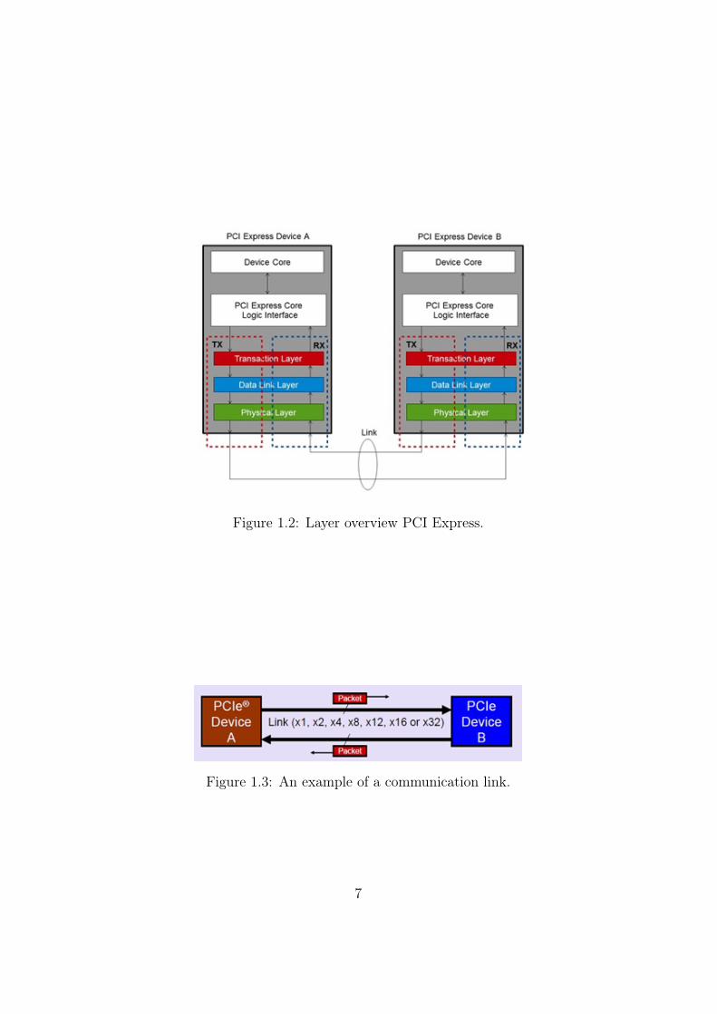
Figure 1.1: New architecture of PCIE link.
Regarding the point-to-point connection, the main drawback is a reductionin the allowable electrical load on the link, but this solution permits a simplermanagement of signals, removing some auxiliary lines from the link as the onefor interrupts and error management, providing also much higher transmissionfrequencies, which can readily migrate to even higher rates.
Serial interconnection between the two devices on a given link results infewer pins per device package, reducing PCI Express chip and board designcost as well as board layout complexity.
5
It is possible to select only some symbol for transmission that matchescertain properties, like an high number of transaction between the logicallevels to facilitate the reconstruction of the clock, and the same number of “1”and “0” within two symbols to maintain roundly constant the DC level of thesignal.
Performance for a given PCI Express link is highly scalable, and this isachieved by implementing more pins and signal lanes in the interconnectionlink. Number of needed lanes will depend on the performance requirementsfor that connection.
Basic PCI Express data rate, referred to one lane, is 2.5 Gb/s for thegeneration 1 (GEN1), 5 Gb/s for the generation 2 (GEN2) and for thegeneration 3 (GEN3) is 8 Gb/s, with the prospective to reach 16 Gb/s withthe future generation 4 (GEN4).
1.2 Features of PCI Express
1.2.1 PCI Express layer architecture
PCI Express architecture will be treated as a layer architecture in this thesis,as shown in Figure 1.2. The software layers generate read and write requeststhat are transported by the transaction layer to the I/O devices using apacket-based, split-transaction protocol [2].
The link layer adds sequence numbers and CRC to these packets in orderto provide an highly reliable data transfer mechanism. Basic physical layerconsists of a dual simplex channel implemented as a transmit pair and areceive pair. The transmit and receive pair together are called lane.
Physical Layer
A PCIe link (Figure 1.3) is the physical connection between two devices andit provides a dual simplex connection, where data are both received andtransmitted simultaneously. It consists of either 1, 2, 4, 8, 12, 16 or 32 pair ofsignals in each direction (because the system uses full differential signalling,so every signal needs two wires) [1].
These signals are referred to lanes. A designer determines how many lanesto implement based on the targeted performance benchmark required on agiven link. The transmission/reception rate for GEN1 is 2.5 Gb/s per laneper direction.
To support a greater degree of robustness in data transmission and recep-tion, each byte of data to be transmitted is translated in a 10-bit code, so
there is a 25% of overhead in order to transmit a single byte of data. Forthe GEN3 and the GEN4 a different transmission encoding scheme is usedtranslating 128 bit into 130 bit, reducing the amount of overhead till 1.5%.
To obtain the values of the aggregate bandwidth presented in Table 1.1 forGEN1, 2.5 Gb/s must be multiplied by 2 (account both directions) and thenby the number of lanes, finally, the number obtained has to be divided by 10( number bits per byte) to achieve the final value expressed bytes/seconds.
A lane consists of signals pair in each direction, a x1 link consists of 1lane in each direction, so there will be a total of 4 signals. A x32 link consistsof 32 lanes in each direction so at the end 128 signals. The link support onlya symmetric number of lanes in each direction.
PCI Express is a packet based transaction protocol; packets are receivedand transmitted serially across all the available lanes of the link at the sametime. The more lanes are implemented on a given link the faster a packet istransmitted and the greater is the bandwidth of the link.
This layer is also responsible for converting a stream of information fromthe data link layer into an appropriate serialized format and transmittingit across the link [3], which is at a certain frequency and width compatiblewith the device on the other hand of the link.
Data link Layer
The primary role of a link layer is to ensure reliable delivery of the packetacross the PCIe link(s), thus its responsibilities is to provide link managementand data integrity, including error detection and error correction.
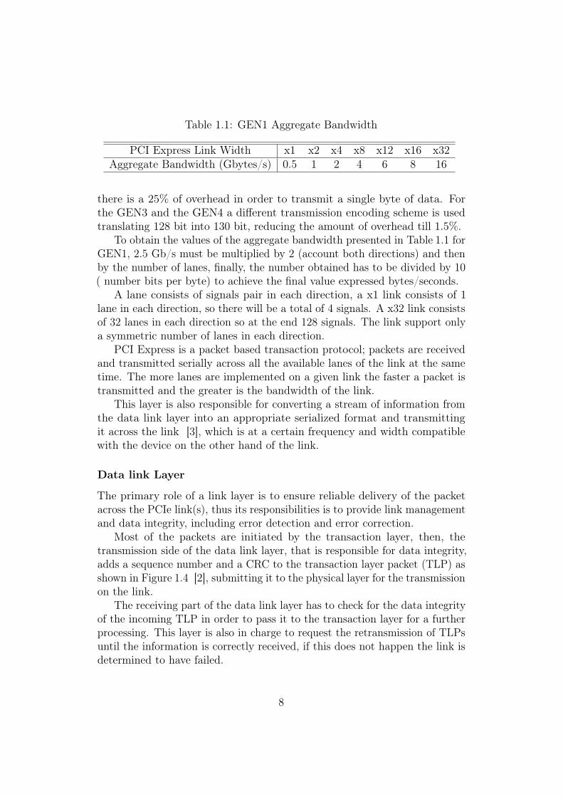
Most of the packets are initiated by the transaction layer, then, thetransmission side of the data link layer, that is responsible for data integrity,adds a sequence number and a CRC to the transaction layer packet (TLP) asshown in Figure 1.4 [2], submitting it to the physical layer for the transmissionon the link.
The receiving part of the data link layer has to check for the data integrityof the incoming TLP in order to pass it to the transaction layer for a furtherprocessing. This layer is also in charge to request the retransmission of TLPsuntil the information is correctly received, if this does not happen the link isdetermined to have failed.
8
Figure 1.4: Formation of TLP packet.
As mentioned before the data link layer handles packets used for linkmanagement functions. In order to differentiate these packets from the normalTLPs is used another term that is data link layer packet (DLLP), whichrepresents the packets that are generated and consumed by the data link layeritself.
Transaction layer
The transaction layer receives read and write requests from the software layersand creates request packets for transmission to the link layer.
In the standard many types of packets such as memory read and writerequests, I/O read and write requests, configuration read and write requests,message requests and completions for split transactions are defined. Thetransaction layer of the protocol is in charge to translate all the requests inone of this type explained above [4].
Memory read and memory write are used to transfer data from or to amemory mapped location. I/O read and write are used to transfer data fromor to an I/O location and these transactions are also restricted to supportinglegacy endpoint devices.
Configuration read and write are used to discover device capabilities,program features and check the status of the PCI Express configuration space.Messages, handled like posted writes, are used for signalling event and generalpurpose messaging.
PCIe transactions can be divided into two categories [1]. Those transac-tions that are posted and those that are non-posted. Non-posted transactions,such as memory reads, implement the split-transaction communication modelused in PCI-X.
9
If a requester device transmits a non-posted memory read request packetto a completer, this device will later send a completion packet with the readdata to the requester. The transaction layer receives the response packetsfrom the link layer and matches them with the original software requests.
Each packet has a unique identifier that enables response packets to bedirected to the correct originator. Posted transactions, like memory write,consist of a memory write packet transmitted from the requester with nocompletion packet to be returned from the completer.
Each request or completion is tagged in a field of the packet called type[4]; each of the packet types is routed based on one of following differentschemes:
• Address routing
• ID routing
• Implicit routing
This layer includes also a credit-based, flow-control protocol which ensuresthat packets are transmitted only when it is known that the buffer on theother end of the link has still some space available, this operation allow toeliminate any packet retries and the associated waste of bus bandwidth dueto resource constraints.
1.2.2 Differential Signalling
The following Figure 1.5 shows the electrical characteristics of the PCI Expresssignal [1]. PCIe devices employ differential drivers and receivers at each port.Unlike a single ended signal whose voltage is compared with the systemground, a differential signal is compared with the opposite mate, thereforewhat is measured is the difference voltage level between them.
Figure 1.5: Electrical characterisc of the PCI Express signal.
Positive voltage difference between D+ and D- terminals implies a logical1, a negative difference implies a logical 0, while no difference means that thedriver is in the electrical idle state or also low power state of the link.
10
The differential peak-to-peak voltage at the transmitter can take valuesbetween 0.4V to 0.6V, while the common mode voltage can be any voltagebetween 0V to 3.6V. Two devices at opposite ends of a link may supportdifferent DC common mode voltages.
1.3 PCI Express Topology
A fabric is composed of point-to-point links that interconnect a set of compo-nents [3]. An example fabric topology is shown in Figure 1.6. All devicesare mapped into a configuration space such that for each one, there will beassociated a certain device number.
Figure 1.6: PCI Express topology and fundamentals devices.
1.3.1 Root Complex
A Root Complex (RC) connects the CPU and memory subsystem to the PCIExpress fabric.
It may support several PCI Express ports as shown in Figure 1.6. Eachport is connected to an endpoint device or else to a switch which forms asub-hierarchy containing one or more switch and endpoints.
The RC generates transaction requests on behalf of the CPU, it transmitspackets out of its ports and also receives packets into its ports forwardingthem to the memory or the CPU.
11
Unlike the rules for a switch, a root complex is generally permitted tosplit a packet into smaller packets when routing transactions peer-to-peerbetween hierarchy domains, for example, split a single packet with 256 bytesof payload in two packets of 128 bytes of payload each [3].
A root complex has a bus Number, device number and function number,which are used to form requester ID or completer ID for its transactions. AHierarchy is the network or fabric of all the devices and links associated witha root complex, that are either directly connected to the root complex via itsport(s) or indirectly connected via switches and bridges.
1.3.2 Endpoints
Endpoints are devices other than root complex and switches that are requestersor completers of PCI Express transactions. They are peripheral devices suchas Ethernet, USB or graphics devices.
Endpoints initiate transactions as a requester or respond to transactionsas a completer. Inside a PCI Express system two types of endpoints can befound:
• PCI Express endpoints
• Legacy endpoints
Legacy Endpoints may support IO transactions, and may support lockedtransaction semantics as a completer but not as a requester. Interrupt-capable legacy devices may support legacy style interrupt generation usingmessage requests, but must also support MSI generation using memory writetransactions.
PCI Express (native) Endpoints must not support IO or locked transactionsemantics and must support Message Signaled Interrupt (MSI) style interruptgeneration. Each endpoint is initialized with a device ID (requester ID orcompleter ID) which consists of a bus number, device number, and functionnumber.
A requester is a device that originates a transaction in the PCIe fabric.The RC and endpoints are examples of requester devices.
A completer is a device addressed or targeted by a requester. A requesterreads data from a completer or writes data to a completer. The Root Complexand endpoints are examples of completer devices.
A Port is the interface between a PCI Express component and the link,and consists of differential transmitters and receivers. An Upstream Port is aport that points in the direction of the RC.
12
A Downstream Port is a port that points away from the RC. An IngressPort is a port that receives a packet, while an Egress Port is a port thattransmits a packet.
1.3.3 Switch
A Switch can be thought as two or more logical PCI-to-PCI bridges, eachbridge is associated with a switch port as illustrated in Figure 1.7, while aPCI Express-to-PCI-X bridge is a bridge between PCI Express fabric and aPCI or PCI-X hierarchy.
Figure 1.7: PCI Express switch structure.
These bridges are internally connected via a non-defined bus. One switchport labelled as an upstream port, points in the direction of the RC. All otherports pointing away from the RC are downstream ports.
Switches forward packets based on one of the three routing mechanismsmentioned before, two of which, address routing and ID routing, are carriedforward from PCI, while the so called implicit routing is new with PCIExpress.
All of the logical bridges residing inside the switch implements a PCIconfiguration header 1, which contains registers for base and limit addressesdownstream, as well as for the bus numbers contained in their domain.
A Switch, in order to determine packet routing and forwarding uses theseregisters. When it forwards a packet, as opposed to the RC, it cannot split a
13
packet into smaller packets, thus if there is a packet of 256 bytes of payload,this as to be forwarded in its size and it cannot be divided in two packets of128 bytes of payload each.
1.4 PCIe Evolution
In the next years a huge increase of the data traffic managed by data centresis expected [5]. Thus PCIe can be used to implement new data-centerarchitectures, since it allows high data transfer rate, and a rapid technologicalevolution, because its performance significantly improves every time a newgeneration is commercially available.
In fact, one of the major features of PCIe is its scalability, passing from arate of 2.5 Gb/s in GEN1 to 8 Gb/s in GEN3, with the aim to reach 16 Gb/swith the future GEN4, that is going to be standardized in few months.
When PCIe is used to interconnect two components that are far, thisfeature could be limited by the choice of the medium utilized for the connection.Copper cabling solutions appeared in the market in a variety in channel widthsto provide connectivity [6].
Some solutions based on copper cables were able only to meet the basicneed of the emerging external expansion applications for GEN1 and GEN2.
Since one of the main goal of an external application is distance, thesesolutions based on copper cables were limited, because they reach lowerdistances with the increasing of data rates, and become bulky in size andweights for GEN3.
Thus PCI SIG released the external cabling specifications [7] includingfiber optical communications to extend the PCIe-based links, achieving remotedata interconnection.
Fibre optic technology provides a better solution for this high data ratechannel, with the possibility to increase the distance of the link and to havehigher performances in terms of Bit Error Rate (BER) with a lower size andweight.
Using optical solutions, a remote connection can be achieved. This al-lows users to leverage the ubiquity of PCIe for many applications such asmemory/disk system interconnects, high-end audio/video applications, highperformance computing and multi-chassis system interconnects [6].
Optical solutions can be a key enabler for network and computer architectswho see value in using PCIe as an I/O technology for data center connectivity.
Using PCIe to connect servers, switches and storage elements can loweroverall system costs by reducing or eliminating the number of protocol con-version chips.
14
1.5 Fiber Optical Technology applied to PCIExpress
1.5.1 Example of Optical Application Using PCIe
Since 2007 when the PCI SIG released the external cabling specificationto interconnect PCI Express systems in GEN1 and GEN2 [6], differentcompanies tries to find out solutions based on optical communication forintra-data center infrastructures.
One of the most important example on which nowadays a lot of articlesare based on, is the demonstration performed by PLX Technology and AvagoTechnology in 2007, that (as shown by the measurement presented in Fig-ure 1.8, where it could be seen the serializer/deserializer (serdes) eye diagram)implements successfully a x8 (8 lanes) link over 30 meters of OM3 MMF inGEN3.
Figure 1.8: Serdes eye diagram.
The setup of the experiment included a host PC housing a PLX designedadapter card employing a GEN3 switch, called PEX8748, mated with a seriesoptical transmitter and receiver modules called AFBR-81/82 used for short-range parallel multi-lane data communication and interconnect applications.These high density optical modules are designed to operate over MMF systemsusing a nominal wavelength of 850 nm for the optical radiation.
At the opposite end of the optical link, a second switch card with anotherpair of AFBR-81/82 series optical transmitter and receiver modules reside ona distribution board to provide fan-out and upstream data aggregation forexpress peripherals.
Different manufacturers like Avago, nowadays produces optical interfaces
15
that could be used for this particular PCIe use, such as Finisar, FCI andSamtec.
In the reported example the connection reach (30 m) is strongly limitedby the technological choice regarding the operating sources and the MMF.
In this thesis, taking a cue from these kind of experiments, we willpropose different technological approach to overcome the physical propagationlimitations and demonstrate an effective remotization thanks to the fiber.
1.5.2 PCI Express and Optical Technology
Today, there is no complete specification for PCIe over optical interfaces [8]because current optical interfaces are not optimized for PCIe use and theyare often designed for other standards. This leads to various issues in theimplementation of the protocol by means the optical medium:
• Supported ranges of frequency
• Latency
• Lane delays
• Sideband signals
• Serializer/deserializer (serdes) levels and impedance
Future cable specification such as OCuLink, that is intended to be a low-cost,small cable form factor for PCIe internal and external devices, offering bitrates starting at 8 Gb/s, with headroom to scale, in combination with PCI3.0 cable specification [3] will regulate all these questions.
Many types of optical interfaces can be used such as Small Form-factorPluggable (SFP), Quad Small Form-factor Pluggable (QSFP), mini-sas HDand mini POD (Figure 1.9).
(a) (b) (c)
Figure 1.9: Optical interfaces: (a) SFP, (b) mini sas-HD, (c) mini POD
16
In many optical applications, the lane generally terminated at 50/100 ohmremaining active at all times, even in case where there is no power on thelink. Optical links may not accurately indicate the presence of a valid PCIereceiver at the opposite end of the link.
If the receiver detection circuitry does not see the appropriate impedance,as said in the PCIe standard, it will not begin the link training, maintainingthe transmitter in the detect state, or sometimes it could link but not others,or some lanes may link and others not, thus reducing the link width.
In order to solve this problems it is possible to have the ability to maskreceiver detection of the PCIe receiver on the other end of the link.
This is done for example in the PEX family of switches that have theability to mask receiver detection and instead use the decoding of incomingdata as a means for link negotiation.
Another factor that can cause problems while using optical technology isthe so-called quite or idle time, that is the period of time where there is notraffic on the link.
This period occurs in different situation:
• When the link is between detect and sending training sequences
• If the link goes in electrical idle because of power management
• If link is retraining cause of link speed or link width changes
The most significant result is that the absence of an optical modulation cansaturate the PIN diode at the receiver and a potential false detection oftraining sequence bits can occur. Noise on the link can also confuse PCIeserdes, causing a delay of the linkup that could be in the order of someminutes.
To prevent these problems a user can perform different actions:
• Disable Active State Power Management (ASPM) avoiding these lowpower states setting some registers directly in the device
• Disable, if possible, the autonomous link speed/width changes settingsome device registers
• If possible, reduce detect quite wait time that requires the access tophysical settings
• Using well designed squelch (a circuit function that acts to suppressoutput of a receiver in the absence of a sufficiently strong desiredinput signal) or Automatic Gain Control (AGC), that is a method of
17
automatically adjusting the gain of the receiver to maintain constantaverage output level for wavelength stream in an optic fiber, to improvethe linkup
• Keep the link active to avoid the need for squelch or AGC, since if theyare not well designed can cause issues, like missing a training sequence,and add delays
Moreover, optical interfaces may require lower input levels to preventreceiver saturation, thus, in order to obtain the best possible eye, the usershould tune the transmitter and receiver parameters preventing auto-tuning,which could be get away with just setting start values of Continuous TimeLinear Equalizer (CTLE) and allowing CTLE tuning in some cases.
In addition to disabling receiver detection, if possible, is used the inferredelectrical idle detection, that is an alternative method to enter in electrical idlestate, which does not need an analog circuitry to perform receiver detection,but is based on windows of time within data are expected.
Down-train disable is another action that must be done to use PCIethrough the optical medium to inhibits width reduction, this action requiresthe access to physical registers and is only needed on one end of the link.
Down-train disable forces retrain if needed, for example when link trainingfail on some lanes because that optical lane is not ready.
Within the PEX family of switches, mentioned before, provisions are madeto ignore the standard electrical idle stimulus, while tracking specific datasymbols to allow link speed negotiation.
PCIe protocol also includes some sideband signals that should be handledsimultaneously to data transmission, but optical interfaces may not have thecapability to do it. For instance, CREFCLK, the 100MHz Cable ReferenceClock, is not needed since the clock is recovered from the data stream by thePCIe transceivers [6].
In addition, also the following electrical power pins are not applicablewhen using an optical cable:
• CPERST – the cable PERST cable platform Reset pins
• CPWRON – the upstream subsystem’s power valid notification
• CPRSNT – the cable installed/downstream subsystem powered-up
• CWAKE – the power management signal for wakeup events
An option to push down in optic this low frequency sideband signals is touse a spare optical link(s), but this would cost an increase in the price ofinterfaces.
18
In conclusion, to get linkup working with optical fiber, one must followthe following steps:
• Switch to inferred electrical idle
• Mask receiver detect
• Disable down-train
• Tune the eye using serdes CTLE changes
• Tune active optical cable (AOC) output, but this usually does not helptoo much
• Reduce detect quiet wait time that reduces optical module saturation
As mentioned before, a link constituted by optical cables could reachlonger distances respect to the copper cables case.
In the following Chapter we will study the maximum remotization achiev-able thanks to a fiber link, taking into account the latency introduced duringthe propagation.
As reported in PCI SIG [8] documents, this latency eventually affectsthe Ack/Nack mechanism included in the PCIe operation, limiting the perfor-mance of the system.
19
Chapter 2
Reach Limitation of thePCIe-based FiberInterconnections
In this chapter we will discuss what are the different causes of the limitationsin the design of a PCIe-based optical link. In general these limitationscould be given either by the propagation medium involved in the link,
either by the protocol itself. Different tables obtained by the analysis of somedata taken directly from the PCI Express standard specification [3] will bethen presented to discuss the protocol impairments.
These tables exhibit what is the maximum reachable distance for a PCIe-based link operating at the a rate of the first three generations.
2.1 Physical Layer Limits
As reported in the previous chapter, the migration of the PCIe over opticalfibre brings many benefits, principally the possibility to reach higher rateof transmission and to cover longer distances, thus allowing to proposenew solutions based on PCI Express links for inter and intra-data centercommunications.
On the other hand, longer optical cables bring to an increase of theattenuation of the signal and add delay [6], so add latency. The attenuationdepends on the operating wavelength as shown in Figure 2.1 [9].
Nowadays, commercial solutions are based on the use of MMF linksand optical sources within the first optical communications window (800 <λ < 900nm), where there is an high attenuation, that is around 2 dB/km.Moreover, the use of MMF links induces the problem of modal dispersion.
20
Figure 2.1: Fiber attenuation versus light wavelength characteristics.
In fact, for these two factors, solutions that work with MMF links at 850nm employing low-cost elements like the Vertical Cavity Surface EmittingLasers (VCSELs) provide a link length limited to few meters [6].
In order to get higher link length, the exploitation of Single Mode Fiber(SMF) links and optical sources emitting in the second (1250 < λ < 1350nm)or in the third window (1500 < λ < 1550nm) is preferred.
In this thesis we target few-km distances: choosing second or third windowsources, attenuation does not affect dramatically the link budget of the system(α1310nm = 0.35dB/km and α1550nm = 0.2dB/km).
Operations carried out around 1550 nm can induce the problem of chro-matic dispersion that getting higher with the rate could be really empathized,thus limiting the maximum reach specially for GEN3 (8 Gb/s) and futureGEN4 (16 Gb/s).
A good trade-off can be achieved by employing optical transceiver modulessuch as SFP+ operating at 1310 nm, where the chromatic dispersion isnegligible for SMF and the attenuation is still acceptable for the provideddistances.
2.2 Protocol Limits
PCIe was natively introduced for a chip-to-chip interconnection and not tocover long distances.
21
Experiment implementations working with a wavelength of 1310 nm, arenot limited in reaching long distances by the physical layer itself, but by somelatency requirements included in the protocol.
In fact as mentioned in the presentation "PCIe Over Fiber Optic: Chal-lenges and Pitfalls" [8], some strict latency requirements related to theAck/Nack mechanism are provided by the PCIe protocol.
In the next paragraphs there will be presented how this mechanism operatesand how it could influence the maximum link length, presenting also sometables, which report depending on the design of the PCIe system what is themaximum distance achievable using a PCIe-based link.
2.3 Ack/Nack Mechanism
The packet that is sent across the link is called TLP, as already seen in theparagraph 1.2.1 of the Chapter 1. It is prepared for the transmission by thedata link layer that applys a sequence number, then calculates and appendsthe link CRC (LCRC), which is used to ensure the integrity of TLPs duringtransmission across a link from one component to the other.
TLPs are stored in a retry buffer inside the TLP transmitter, and arere-sent unless a positive acknowledgement of receipt is received from the othercomponent [3]. If repeated attempts to transmit a TLP are unsuccessful,the transmitter will determine that the link is not operating correctly, andinstructs the physical layer to retrain the link.
If link retraining fails, the physical layer will indicate that the link is nolonger up. A variety of counters and timers are used in the mechanism to setup the TLP LCRC, to determine the sequence number and to support datalink layer retry.
The REPLY_TIMER is the element that is used in this work to understandthe limitation on the maximum link length given by the Ack/Nack mechanism.
This timer counts the period of time that determines when a replay isrequired, according to the following rules [3]:
• Started at the last symbol of any TLP transmission or retransmission
• For each replay, reset and restart REPLAY_TIMER when sending thelast symbol of the first TLP to be retransmitted
• Resets and restarts for each Ack received while there are more unacknowl-edged TLPs outstanding, if, and only if, the received Ack acknowledgessome TLP in the retry buffer
22
• Reset and hold until restart conditions are met for each Nack received(except during a replay) or when the REPLAY_TIMER expire.
• Not advanced during link retraining.
• Resets and holds when there are no outstanding unacknowledged TLPs
A replay can be initiated by the expiration of the REPLAY_TIMER, orby the reception of a Nack.
The following rule covers the case of the expiration of the REPLAY_TIMER:
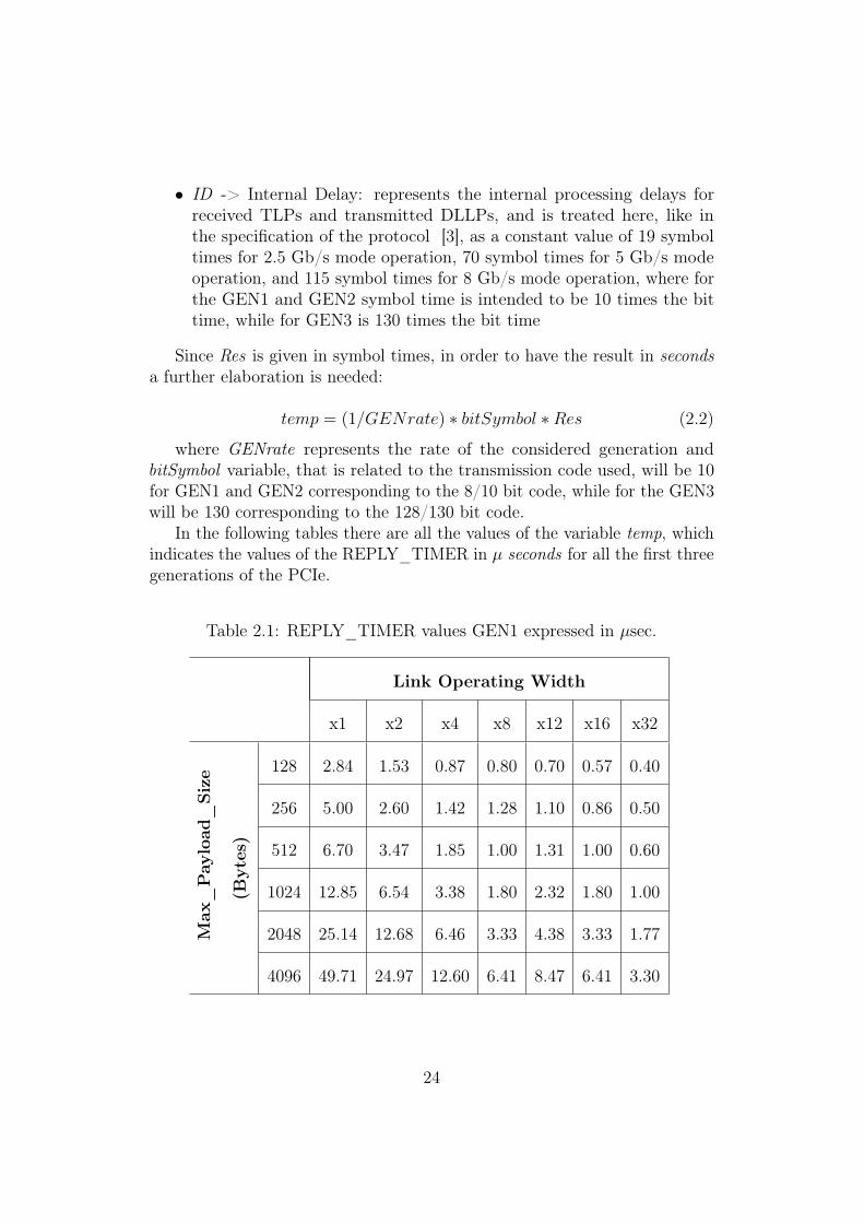
• If the transmitter retry buffer contains TLPs for which no Ack or NackDLLP has been received, and (as indicated by REPLAY_TIMER) noAck or Nack DLLP has been received for a period exceeding the timeindicated in Table 2.1 for GEN1, Table 2.2 for GEN2 and Table 2.3 forthe GEN3, the transmitter initiate a reply
2.4 REPLY TIMER Values
The values for the REPLY_TIMER, as presented in the standard [3], arecalculated using the following formula:
Res = ((MPS + TLPOH) ∗ AF )/LW ) + ID) ∗ 3 (2.1)
where:
• MPS -> Maximum Payload Size: is the value in the Max Payload Sizefield of the device control register that is set at the initialization of thesystem and it represents the maximum number of bytes for the payloadthat can be accepted by a device; this value will correspond to the lowerMPS of all the devices in the final system topology
• TLPOH -> TLP Overhead: represents the additional TLP componentswhich consume link bandwidth and it changes based on the generationused as explained in paragraph 1.2.1
• AF -> Ack Factor: represents the number of maximum size TLPswhich can be received before an Ack is sent, and is used to balance linkbandwidth efficiency and retry buffer size.
• LW -> Link Width: is the operating width of the link
23
• ID -> Internal Delay: represents the internal processing delays forreceived TLPs and transmitted DLLPs, and is treated here, like inthe specification of the protocol [3], as a constant value of 19 symboltimes for 2.5 Gb/s mode operation, 70 symbol times for 5 Gb/s modeoperation, and 115 symbol times for 8 Gb/s mode operation, where forthe GEN1 and GEN2 symbol time is intended to be 10 times the bittime, while for GEN3 is 130 times the bit time
Since Res is given in symbol times, in order to have the result in secondsa further elaboration is needed:
temp = (1/GENrate) ∗ bitSymbol ∗Res (2.2)
where GENrate represents the rate of the considered generation andbitSymbol variable, that is related to the transmission code used, will be 10for GEN1 and GEN2 corresponding to the 8/10 bit code, while for the GEN3will be 130 corresponding to the 128/130 bit code.
In the following tables there are all the values of the variable temp, whichindicates the values of the REPLY_TIMER in µ seconds for all the first threegenerations of the PCIe.
Table 2.1: REPLY_TIMER values GEN1 expressed in µsec.
Link Operating Width
x1 x2 x4 x8 x12 x16 x32
Max
_Pay
load
_Siz
e
(Byt
es)
128 2.84 1.53 0.87 0.80 0.70 0.57 0.40
256 5.00 2.60 1.42 1.28 1.10 0.86 0.50
512 6.70 3.47 1.85 1.00 1.31 1.00 0.60
1024 12.85 6.54 3.38 1.80 2.32 1.80 1.00
2048 25.14 12.68 6.46 3.33 4.38 3.33 1.77
4096 49.71 24.97 12.60 6.41 8.47 6.41 3.30
24
Table 2.2: REPLY_TIMER values GEN2 expressed in µsec.
Link Operating Width
x1 x2 x4 x8 x12 x16 x32
Max
_Pay
load
_Siz
e
(Byt
es)
128 1.73 1.07 0.74 0.70 0.65 0.59 0.50
256 2.80 1,61 1.01 0.95 0.85 0.74 0.57
512 3.66 2.04 1.23 0.82 0.96 0.82 0.62
1024 6.73 3.58 2.00 1.21 1.47 1.21 0.81
2048 12.88 6.65 3.53 1.97 2.50 1.97 1.19
4096 25.16 12.79 6.60 3.51 4.54 3.51 1.96
Table 2.3: REPLY_TIMER values GEN3 expressed in µsec.
Link Operating Width
x1 x2 x4 x8 x12 x16 x32
Max
_Pay
load
_Siz
e
(Byt
es)
128 16.23 10.92 8.24 7.95 7.51 7.02 6.29
256 24.96 15.26 10.43 9.90 9.68 8.19 6.87
512 31.93 18.77 12.19 8.87 9.99 8.87 7.21
1024 56.89 31.25 18.43 11.99 14.14 11.99 8.77
2048 106.80 56.20 30.90 18.23 22.47 18.23 11.90
4096 206.65 106.13 55.87 30.71 39.10 30.71 18.14
25
2.5 Maximum Link Lengths
Starting from the tables presented in the previous paragraph, showing thelimitation on the maximum link length given by the Ack/Nack mechanism interms of time for the first three generations, we have calculated the maximumlength of the interconnection for the different generations, MPS and linkwidth through the following formula:
Distance = (2 ∗ 108) ∗ temp ∗ 1/2 (2.3)
knowing that the speed of the light in fiber is 2 ∗ 108 m/s and that in the timegiven by the value of the variable temp, the packet has to cover two times thedistance between the transmitter and the receiver.
Distance values contained in the following tables are an important resultthat allows us to design, based on the available MPS and link width, anoptical link providing the maximum possible link length for a PCI Express-based communication system, implementing a connection between two distinctboards.
Table 2.4: Maximum distance reachable in GEN1 expressed in km .
Link Operating Width
x1 x2 x4 x8 x12 x16 x32
Max
_Pay
load
_Siz
e
(Byt
es)
128 0.28 0.15 0.09 0.08 0.07 0.06 0.04
256 0.50 0.26 0.14 0.13 0.11 0.09 0.05
512 0.67 0.35 0.19 0.10 0.13 0.10 0.06
1024 1.29 0.65 0.34 0.18 0.23 0.18 0.10
2048 2.51 1.27 0.65 0.33 0.44 0.33 0.18
4096 4.97 2.50 1.26 0.64 0.85 0.64 0.33
For example if we want to set up a PCI Express system working in GEN3,so at 8.0 Gb/s, with an usual link width of 8 lanes (x8) and a MPS of 1024bytes, according to Table 2.6 a maximum link length of 1.2 km has to bechosen.
26
Table 2.5: Maximum distance reachable in GEN2 expressed in km .
Link Operating Width
x1 x2 x4 x8 x12 x16 x32
Max
_Pay
load
_Siz
e
(Byt
es)
128 0.17 0.11 0.07 0.07 0.07 0.06 0.05
256 0.28 0.16 0.10 0.10 0.09 0.07 0.06
512 0.37 0.20 0.12 0.08 0.10 0.08 0.06
1024 0.67 0.36 0.20 0.12 0.15 0.12 0.08
2048 1.29 0.67 0.35 0.20 0.25 0.20 0.12
4096 2.52 1.28 0.66 0.35 0.45 0.35 0.20
Table 2.6: Maximum distance reachable in GEN3 expressed in km .
Link Operating Width
x1 x2 x4 x8 x12 x16 x32
Max
_Pay
load
_Siz
e
(Byt
es)
128 1.62 1,09 0.82 0.80 0.75 0.70 0.63
256 2.50 1.53 1.04 0.99 0.97 0.82 0.69
512 3.19 1.88 1.22 0.89 1.00 0.89 0.72
1024 5.69 3.13 1.84 1.20 1.41 1.20 0.88
2048 10.68 5.62 3.09 1.82 2.25 1.82 1.19
4096 20.66 10.61 5.59 3.07 3.91 3.07 1.81
27
Chapter 3
Dimensioning and ExperimentalValidation of PCIe-based FiberInterconnections
In this chapter the remotization of the PCIe-based fiber interconnectionbetween two devices according to the protocol requirements is studiedand experimented.
According to the considerations made in the previous Chapter and byemploying commercial devices, a proper design of the PCIe link is proposedto carried out the experimental activity in order to validate these PCIeinterconnections.
In particular, in paragraph 3.3 a brief explanation of some of the principalmeasurements included in the PCIe protocol standard to guarantee thecompliance of the signal are reported.
Finally, all the results of the physical and BER analysis for all the differentPCIe generations are shown.
3.1 Link Dimensioning
As explained in Chapter 2, in order to have a good trade-off between atten-uation and chromatic dispersion, we choose to exploit a commercial SFP+optical transceiver module designed for data centre applications, based on a1310 nm Distributed Feedback (DFB) laser, in combination with a SMF linkto avoid modal dispersion.
All the generations of PCIe protocol can be tested employing this SFP+transceiver module, able to operate at 8.5 Gb/s and from 9.95 to 11.3 Gb/sbit rates.
28
These kind of transceivers, projected to work in case of a maximum linklength of 10 km, have a mean optical output power of -6 dBm and a sensitivityof -13.5 dBm, thus operating at 1310 nm, where the attenuation is around0.35 dB/km, and propagating only few-km, the link budget remains good,making the signal at the receiver detectable from the noise.
In conclusion, adopting this approach the only impairment on the maxi-mum optical link length is given by the Ack/Nack mechanism of the protocol.
In our experimental setup the choice of the tested link length has beenmade keeping in mind the table presented in Chapter 2.
3.2 System Setup
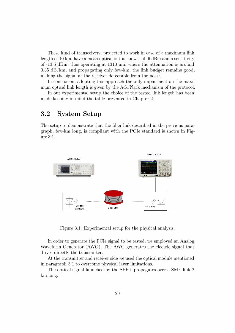
The setup to demonstrate that the fiber link described in the previous para-graph, few-km long, is compliant with the PCIe standard is shown in Fig-ure 3.1.
Figure 3.1: Experimental setup for the physical analysis.
In order to generate the PCIe signal to be tested, we employed an AnalogWaveform Generator (AWG). The AWG generates the electric signal thatdrives directly the transmitter.
At the transmitter and receiver side we used the optical module mentionedin paragraph 3.1 to overcome physical layer limitations.
The optical signal launched by the SFP+ propagates over a SMF link 2km long.
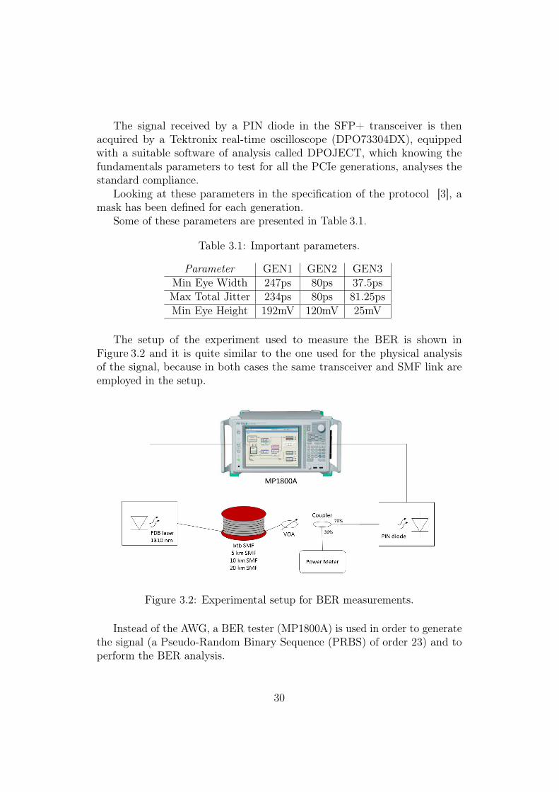
29
The signal received by a PIN diode in the SFP+ transceiver is thenacquired by a Tektronix real-time oscilloscope (DPO73304DX), equippedwith a suitable software of analysis called DPOJECT, which knowing thefundamentals parameters to test for all the PCIe generations, analyses thestandard compliance.
Looking at these parameters in the specification of the protocol [3], amask has been defined for each generation.
Some of these parameters are presented in Table 3.1.
The setup of the experiment used to measure the BER is shown inFigure 3.2 and it is quite similar to the one used for the physical analysisof the signal, because in both cases the same transceiver and SMF link areemployed in the setup.
Figure 3.2: Experimental setup for BER measurements.
Instead of the AWG, a BER tester (MP1800A) is used in order to generatethe signal (a Pseudo-Random Binary Sequence (PRBS) of order 23) and toperform the BER analysis.
30
Moreover, in this scheme also a Variable Optical Attenuator(VOA) and apower meter are introduced.
These elements are inserted in the setup to control the state of the powerentering in the receiver and thus to measure the BER for different values ofthe optical received power.
For this experiment it is important to point out the fact that since thetransceiver in use is built to work at 8.5 Gb/s or around 10 Gb/s, it cannotbe used its clock recovery system, so this functionality has to be disabled.
This fact induces the BER tester to recover externally the clock in orderto calculate the BER.
3.3 Measurements for the Compliance to thePCIe Standard
This paragraph presents a brief explanation of the most important measure-ments provided by the PCIe standard.
The PCI Express base specification includes amplitude, timing, jitter, andeye diagram measurements for the transmitter and the receiver, defines jitterand eye diagram margins at the system level compliance points and representsthe tests performed at plug-fests [10].
The following list encapsulates some of the key measurements (to provecompliance and interoperability) needed to validate system components toinsure they meet the specification:
• Amplitude Measurements
• Timing Measurements
• Jitter Measurements
• RT-Eye Diagrams and Mask Testing
• Noise and Jitter
• Frequency Domain Measurements
• Receiver Sensitivity and Jitter Tolerance Measurements
Amplitude measurements are necessary to guarantee that the signal afterpassing through the transmission medium, achieve proper voltage levels andstability to allow to the receiving circuit the reliable reception of all bits fromthe transmitter.
31
The fundamental parameter given by the specification, regulating thismeasure, is the peak-to-peak differential voltage that guarantees the correctvoltage levels at the transmitter.
The specification gives the minimum transmitted differential voltage,providing that under the worst medium condition, at the receiver there is aminimum voltage level. This value is not given by a traditional peak-to-peakmeasure, but is achieved by means of a PCI Express specific algorithm.
Timing measurements allow to understand if the signal is free from timingvariations and if its transitions are fast enough to preserve the data valuesthat the signal is meant to deliver, so they detect aberrations and signaldegradation that arise from distributed capacitance, crosstalk, and more.
Jitter analysis passes through an evolution with the different generation,so there is not a unique method to measure the jitter.
The original GEN1 PCI Express specification specifies that “Median-Max-Jitter” has to be measured over any 250 consecutive bits [10].
The Median-Max-Jitter is the maximum deviation in the positive ornegative direction of the Time Interval Error (TIE), the time differencebetween the recovered clock (from the data stream) and the data signal [11],this deviation is calculated using the median as the timing reference and ismeasured from an histogram of the TIE over 250 unit intervals, where thereare limits placed around the max and min value of TIE that will representthe Median-Max-Jitter specification.
For the GEN2 and further, in order to measure the jitter is used a dual-Dirac model, that estimates Total Jitter (TJ), Random Jitter (RJ), andDeterministic Jitter (DJ). The TJ measurement is done at a certain BERvalue.
This model relies on five assumption[12]:
• Jitter can be separated into two categories, RJ and DJ defined above.
• RJ follows a Gaussian distribution and can be fully described by therms value of its distribution or the width of the Gaussian distributionitself σ
• DJ follows a finite, bounded distribution
• DJ follows a distribution formed by two Dirac-delta functions where thetime-delay separation of them gives. the dual-Dirac model dependentDJ
• Jitter is a stationary phenomenon that means that a measurements ofthe jitter on a given system taken over an appropriate time interval willgive the same result regardless of when that time interval is initiated
32
Components of jitter are combined through a convolution as show inFigure 3.3.
Jitter distribution can be seen as the histogram of the crossing point ofan eye diagram, this distribution is dominated by DJ at the crossing point, attime delays further from the crossing point is increasingly dominated by RJuntil, far from the crossing point, the tails follow the Gaussian Rj distribution.
The two Dirac-delta functions are positioned at µL and µR. There aredifferent ways to estimate TJ(BER) and the matter that differentiate them ishow the tails of the jitter distribution are described respect to the tails of twoGaussians of width σ separated by a fixed amount DJ(δδ) that is the moduleof the difference of µL and µR.
Figure 3.3: The convolution of two delta functions separated by DJ and aGaussian RJ distribution of width σ.
As it can be seen in Figure 3.4 DJ closed the eye of a fixed amount,DJ(δδ),while, by looking at equation 3.1, the Gaussian RJ tails closed the eyes of anamount that depends on the BER of interest.
Once σ and DJ(δδ) are measured, the eye closure at any BER can beestimated with:
TJ(BER) = 2QBERxσ +DJ(δδ) (3.1)
where QBER is calculated from the complementary error function, forexample if there is a BER of 10 -12 the QBER value is 7. Since this value ismultiplied by σ, the accuracy of TJ(BER) depends on the accuracy of theRJ measurement.
In order to understand the relation between TJ and the BER a few otherthings should be defined. First of all BER is defined as:
BER(x, V ) = limx→+∞
Nerr(x, V )
N(3.2)
where (x,V) represent the position of the sampling point and Nerr(x, V )is the number of errors that would be detected from a total of N transmitted
33
Figure 3.4: Relation between eye diagram and jitter distribution.
34
bits [12]. There is an error detection if a logical ’0’ is observed if the potentialis greater than V at the sampling time delay x.
This dependence on x of the BER is really important for how TJ(BER) isdefined. By scanning the time delay position of the sampling point across theeye, one could build the so called bathtub curve shown in Figure 3.5.
Figure 3.5: Bathtub plot example.
The opening of the eye at a given BER, t(BER), is given by the separationof the left and right BER curves at that specific BER level.
It could be seen how in Figure 3.5 the eye opening at a BER of 10 -12 isgiven by the difference of xL and xR, that are the points on the two curves atthis BER value.
t(BER) = xR(BER)− xL(BER) (3.3)
In conclusion TJ(BER) is intended as the amount of eye closure due to jitterat a given BER level, and it can be calculated as the difference of the bitperiod and the eye opening.
TJ(BER) = TB − t(BER) (3.4)
The “eye diagram”—an oscilloscope display that results from the overlap of aseries of data waveforms—is an important tool for establishing the quality ofthe PCI Express transmitted signal [10].
In order to produce the eye diagram, it is necessary to recover the clockfrom the data to be able to synchronize the data stream carrying random,pseudorandom, or compliance pattern bits.
35
In addition to this operation on the clock, the transmitter and interconnecttest points require that transition bits and de-emphasized bits be separatedand mask testing be performed on each bit type.
Figure 3.6 shows the definition of the mask geometries, as they appear inthe specification.
In this paragraph, all the results of the experimental activity carried out inorder to demonstrate the compliance to the standard of the PCIe-based opticallink designed to target few-km reach, operating at the three generations rates(2.5 Gb/s, 5 Gb/s or 8 Gb/s) for an intra data center interconnection, arepresented.
3.4.1 GEN1 Characterization
Experimental results, obtained for the 1st generation, are exposed in thisparagraph.
The first presented figure, Figure 3.7, shows the view, taken directlyfrom the oscilloscope, of the differential signal received after 2 km of SMFpropagation.
As explained in Chapter 1, the PCIe signal is differential, thus in Figure 3.7we can observe the two components of the signal, the first one and the mate.
36
This figure will not be reported for the other generations since the patternwill be the same, just with different rate.
Figure 3.7: Signal view on the oscilloscope in caso of GEN1 PCIe transmissionat 2.5 Gb/s.
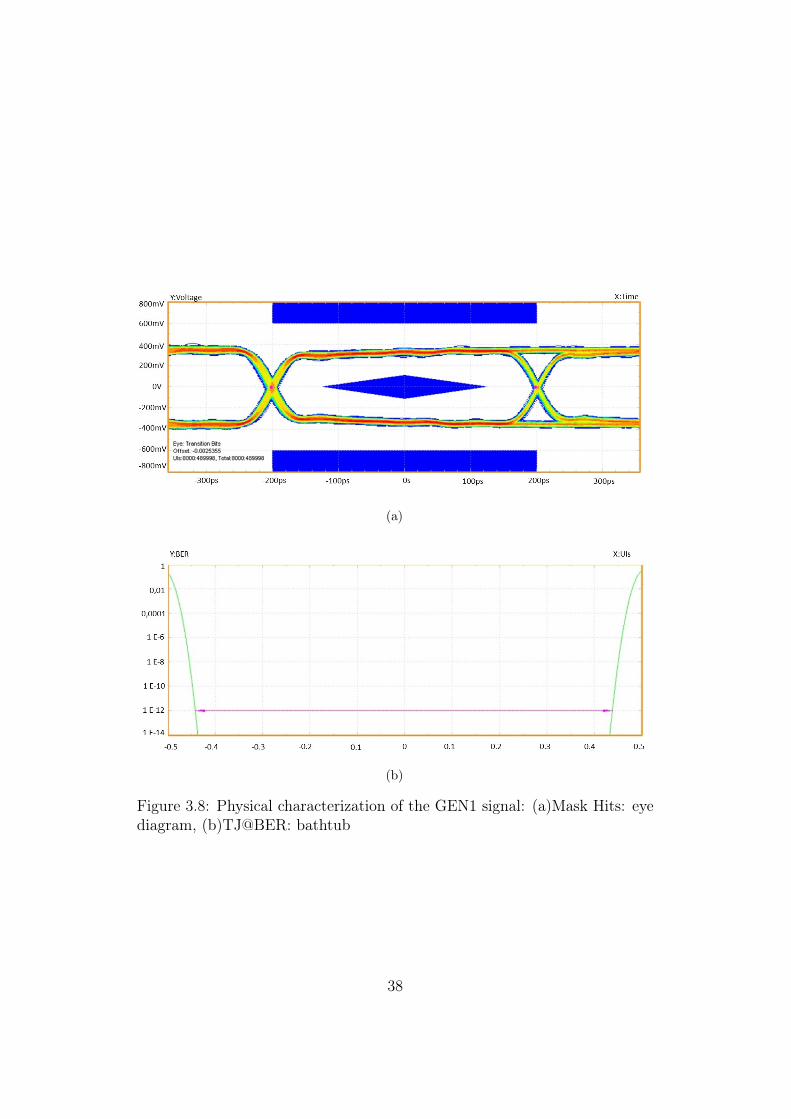
Results reported in Figure 3.8 are referred to the system setup presentedin Figure 3.1.
Figure 3.8 (a) shows the eye diagram obtained from the GEN1 signalreceived after 2 km of SMF propagation, a mask is inserted to allow tounderstand that the signal is conform with the specification; (b) shows thebathtub diagram which reports the real horizontal opening of the eye, asexplained in the previous paragraph.
In this case, after the propagation on the optical link, the vertical eyeopening measured is 566.48 mV, holding a good margin with respect to thelow limit of 192 mV mentioned in Table 3.1.
The horizontal eye opening is 377.42 ps, much greater with respect to thelow limit of 247.00 ps fixed by the specification.
Results presented in Figure 3.9 refer to the BER setup scheme shown inFigure 3.2 .
BER measures are taken even after 5 km of SMF link in order to test themaximum link length that this generation can support, based on Table 2.4.This link length can be reach in case of a x1 link within a system operatingwith a MPS of 4096 bytes.
We can notice that for the GEN1 operations, there are no significantpenalties introduced by propagating in the SMF link with respect to theback-to-back (btb) operation, and also that there are no error floors.
This situation can be achieved because in the link dimensioning we chooseto work around 1310 nm, which is the wavelength where the SMF presentsnegligible dispersion. Another important factor that leads to these results is
37
(a)
(b)
Figure 3.8: Physical characterization of the GEN1 signal: (a)Mask Hits: eyediagram, (b)TJ@BER: bathtub
38
Figure 3.9: Characterization of the BER at different distances for GEN1.
39
the choice of the transceiver, targeting the tested distances in terms of linkbudget.
3.4.2 GEN2 Characterization
In this paragraph the experimental results needed to characterize the fiberlink operating in GEN2 are presented.
(a)
(b)
Figure 3.10: Physical characterization of the GEN2 signal: (a) Mask Hits:eye diagram, (b) TJ@BER: bathtub
Figure 3.10 shows that also for a link operating in GEN2, it can bemaintained the compliance with the physical requirements.
40
Figure 3.11: Characterization of the BER at different distances for GEN2.
41
The bit duration in GEN2 is 200 ps (while the duration in GEN1 is 400ps) so from Table 3.1, GEN2 jitter limits are more strict with respect to theone of the GEN1, but on the other hand a smaller eye it is accepted.
The Total Jitter measured is around 39 ps compared to a maximum valueof 80 ps; the vertical opening of the eye is 520.13 mV, much higher respect to120 mV.
Figure 3.13, referred to the BER setup scheme, presents the BER measuresperformed for the GEN2 operation.
For this generation the BER is measured in the btb conditions and aftera propagation of 2 km of SMF, that as specified in Table 2.5 is almost themaximum reach in case of GEN2 link.
As for the first generation we see that there are no error floors or significantpenalties introduced by propagating in the SMF link with respect to theback-to-back operation.
Also in this case, for GEN2 operation, adopting the proposed solution,the few-km fiber link works and it is compliant with the standard.
3.4.3 GEN3 Characterization
This paragraph is dedicated to the characterization of the third generation ofthe protocol.
Keeping in mind that the bit time in GEN3 is 125 ps, it can be seen thatthe PCIe standard accepts for the third generation a smaller eye, but providesalmost the same requirement on the Total Jitter.
TJ measured after a propagation of 2 km on the SMF link is around 32.9ps, this result leads to an horizontal eye opening of 92.1 ps, that is muchhigher respect to the low limit reported in Table 3.1.
The vertical eye opening measured is 538.18 mV with respect to an allowedminimum value of 25 mV.
Based on Table 2.6, for this generation it has been performed the BERcalculation in three cases:
• back-to-back condition
• 10 km of SMF link: predicted for an interconnection that implements alink of 1 lanes within a system that supports a MPS of 2048 bytes andfor an interconnection that employs a 2-lanes link inserted in a systemoperating with MPS of 4096 bytes
• 20 km of SMF link: achievable using a x1 link width within a systemhandling with packets with a MPS of 4096 bytes
Figure 3.13: Characterization of the BER at different distances for GEN3.
44
From Figure 3.13, also using a link operating at 8 Gb/s, there are no errorfloors or significant penalties introduced by propagating in the SMF link withrespect to the back-to-back operation.
It is necessary to specify that using this SFP+ optical transceiver moduleto exploit a SMF link of 20 km, the sensitivity provided by the receiver isstill enough to reach a good BER quality.
3.4.4 Conclusions
Due to the dimensioning of the link explained at the beginning of the Chapter,it has been demonstrated through a physical and BER analysis of the signalreceived after a propagation on a SMF link, that it is possible to design afew-km PCIe-based interconnection for all the three generations standardizedof PCIe.
Thanks to the technological implementation proposed for our test, thecompliance with the standard has been experimentally described, showing areal remotization according to the protocol limitation studied in the Chapter2, targeting the typical distances necessary for datacom applications.
45
Chapter 4
Generation 4 Analysis andExpectation
In this chapter, we take into account the future 4th generation of the PCIExpress that will operate at 16 Gb/s.
With the incoming of this new generation the optical technology becomesessential since using copper cables at this rate, the link length will be stronglylimit to few meters [13].
Based on the discussion made in Chapter 2 on the physical layer impair-ments, an explanation of the choice of the elements employed to perform thisnew experimentation will be given.
A standard for this new generation is not still present. Hence, we proposea prediction on the maximum link lengths that can be obtained operating at16 Gb/s for different system designs according to all the indications given byPCI SIG documents regarding the standardization and the rules adopted forthe previous generations.
Finally, to demonstrate the feasibility of a few-km PCIe-based opticalcommunication link operating in GEN4, a suitable experimental is presented.
4.1 Link Dimensioning
As presented in Chapter 3, in order to have a good trade-off between attenua-tion and chromatic dispersion, we employ also for GEN4 a commercial SFP+optical transceiver module, including a 1310 nm DFB laser, in combinationwith a SMF link to avoid modal dispersion.
In order to provide modulation at 16 Gb/s, we adopt a special SFP+transceiver module proposed for Fibre Channel applications, for covering upto 10 km distances, with a modulation bandwidth of 14 GHz.
46
Since the operating rate of this element does not match the rate of GEN4,some problems with jitter are introduced, but according to PCI SIG indications[14], this limitation can easily be compensated by the use of a simple 2-tapsDecision Feedback Equalizer (DFE) expected in the future standardization ofthis generation.
Of course, a proper optical transceiver working at 16 Gb/s can overcomethis limitation.
Setting up the link in this way, the only factor that limits the intercon-nection length is given by the Ack/Nack mechanism of the protocol.
4.2 Link Lengths Expectations
In this section, protocol impairments to the link are discussed.Generation 4 is still under standardization by PCI SIG, so the values of
the REPLY_TIMER of the Ack/Nack mechanism used in chapter 2 for theother generations are not yet available. This fact does not prevent to make aprediction on the maximum reachable distance that could be covered by alink operating in generation 4.
Knowing that for the GEN1 and the GEN2 there is the same transmissioncoding scheme, as explained in Chapter 1, and that GEN2 works at the doubleof the rate of GEN1, starting from the third generation of PCI Express wededuced the maximum reachable distance for the new generation 4.
In fact, between GEN3 and GEN4 there are the same common character-istics mentioned above for the first two generations, thus supporting a sort ofparallelism between the relations GEN1-GEN2 and GEN3-GEN4.
Looking at the tables of distances built for GEN1 and GEN2 there is nota specific deterministic relation between their values, but we noticed that allthe row, corresponding to a certain MPS value in generation 1, are replicatedalmost identically at the next MPS value in the Table 2.5 for GEN2.
For example the row corresponding to an MPS of 128 bytes in Table 2.4is replicated in the row corresponding to an MPS of 256 bytes in Table 2.5.
In order to achieve Table 4.1 for the new generation, we adopt the sameoperation of "duplication" and "translation" starting from the table of GEN3.
There is an exception for the row corresponding to 256 bytes of MPS inTable 2.4 that does not follow this rule and it is not replicated in the rowcorresponding to 512 bytes of MPS in Table 2.5.
To be able to understand how to build the expectation distances forGEN4 also for this row, we analysed the relation between the diagonals inthe precedent tables.
47
Table 4.1: Maximum distance reachable in GEN4 expressed in km .
Link Operating Width
x1 x2 x4 x8 x12 x16 x32
Max
_Pay
load
_Siz
e
(Byt
es)
128 1.25 0.87 0.72 0.67 0.67 0.63 0.57
256 1.62 1.09 0.82 0.80 0.75 0.70 0.63
512 1.82 1.22 0.89 0.74 0.80 0.74 0.69
1024 3.19 1.88 1.22 0.89 1.00 0.89 0.72
2048 5.69 1.84 1.20 1.41 1.41 1.20 0.88
4096 10.68 5.62 3.09 1.82 2.25 1.82 1.19
Many elements on these diagonals are similar, so our approach assumethat if there is a value in the new table for GEN4, obtained from the operationexposed before, where it is possible, it can be replicated on the diagonal.
This operation does not work for all the elements. In fact, the differencebetween two elements in the diagonal for the GEN1 is the double respect tothe difference of two elements in the diagonal of GEN2 table.
Based on these relations we deduced the first and the third rows ofTable 4.1, but in order to calculate the last value of the first row, so the onethat is obtained having an MPS of 128 bytes and a link of 32 lanes, we tookthe difference in all the other tables between the element in this position andthe element that gives the maximum distance reachable for a system that hasan MPS of 256 bytes and 32 lanes.
4.3 Characterization of the GEN4 Signal
In the following paragraph the setup for the physical analysis of the signal isreported. Then, all the measurements that has been carried out to demonstratethat after a SMF link of few-km is still possible to match all the physicalcharacteristics of a PCI Express signal are reported.
In particular, based on Table 4.1, the results after a propagation on SMFlinks of 2 km and 10 km are presented. 10 km reach is the maximum GEN4distance which can be covered in a system with a MPS of 4096 bytes that uses
48
1-lane links, according to our evaluation described in the previous paragraph.
4.3.1 System Setup
Figure 4.1 shows the setup of the system for the physical analysis of thesignal at 16 Gb/s, where the interconnection link is implemented employingthe components discussed in the link dimensioning paragraph. The devicesinvolved in this system are quite the same respect to those used in the setuppresented in the previous Chapter in Figure 3.1.
Figure 4.1: Experimental setup for the physical analysis of the GEN4 signal.
In order to produce the signal at 16 Gb/s, a Matlab script producing aPRBS long 127 bits was used.
The PRBS signal generated by the script is uploaded to the AWG todirectly drive the optical transceiver module. The optical signal is receivedwith a PIN diode.
Tektronix real-time oscilloscope (DPO73304DX) is then inserted in orderto understand if the received signal is compliant with the specifications thatwe have deduced for the future standard [14].
All these instruments involved show a sufficient bandwidth to supportoperation even at 16 Gb/s (for example the oscilloscope employed has abandwidth of 33 GHz).
49
4.3.2 Measurements Results
Figure 4.2 (a), 4.3 (a) and 4.4 (a) represent respectively the 16 Gb/s detectedeye diagram in btb operation and after 2 km and 10 km of propagation alongthe SMF link.
By looking at these figures the full compliance with the protocol eye mask,deduced using the GEN4 previews given in the last PCI SIG conference [14],can be noticed.
(a)
(b)
Figure 4.2: GEN4 signal characterization in btb operation mode: (a) eyediagram with the mask (b) bathtub curve.
In Figure 4.2 (b) and 4.3 (b), that represent the bathtub curves, the realhorizontal eye opening at a BER value of 10 -12 is shown.
The horizontal eye opening after 2 km of propagation in a SMF link is 25
50
(a)
(b)
Figure 4.3: GEN4 signal characterization after 2 km of SMF link: (a) eyediagram with the mask (b) bathtub curve.
51
(a)
(b)
Figure 4.4: GEN4 signal characterization after 10 km of SMF link: (a) eyediagram with the mask (b) histogram of the jitter.
52
ps, with a consequent measured jitter of 37 ps. These value of jitter is quitehigh respect to the effective time of a bit for GEN4 (62.5 ps).
This problem is more accentuated after 10 km of propagation and is mainlydue to the exploitation of a transceiver with a limited bandwidth.
The solution to solve this issue, as described previously, is the exploitationof a 2-taps DFE that is expected with the incoming standardization of GEN4or the employment of new SFP+ optical transceiver modules operating at 16Gb/s.
Figure 4.4 presents an example of a jitter histogram. Looking at this figureit can be seen how the jitter components are distributed.
There are not two distinct peaks in this case, such as shown in Figure 3.3,because the deterministic component is much lower respect to the randomcomponent of the jitter.
4.4 BER Characterization
4.4.1 System Setup
Figure 4.5: Setup of the system which has been employed to perform BERmeasurements.
The scheme presented in Figure 4.5 shows the instruments exploited tocarried out the BER measurements.
The setup, as explained in the previous physical analysis experiment, isrealized using a SMF link and a SFP+ optical transceiver module operating
53
at 14 Gb/s.Since the BER tester (MP1800A) employed in the experiment has a
bandwidth of 12 GHz and the sequence of data in GEN4 runs at 16 GHz, inorder to perform the BER measurements a demultiplexer (SHF 423 DEMUX)is introduced to scale the output signal.
This demultiplexer can operate with data rate from 2 Gb/s up to 60 Gb/s.In this case the instrument divides the input data stream of 16 Gb/s intofour parallel data streams of 4 Gb/s.
The signal to be checked by the MP1800A is a PRBS of order 7, sequencegenerated, as explained previously, using a Matlab script based on the samePRBS generator logic provided by the BER tester.
The signal received by the transceiver, is given as the input data streamto the demultiplexer. One of the four output of the demultiplexer is the inputdata stream for the BER test to finally measure the BER.
4.4.2 BER Results
Figure 4.6 shows that there is not a significant degradation of the BER qualityalso for few-km distance.
There is no penalties introduced by the propagation in the SMF connec-tions and no error floors. It can be concluded that the performances, in termsof BER, are the same for the different lengths of the link.
For example if the received power is assumed to be -20 dBm, the valuesof the BER are: 1.5 x 10⁻⁵ in the btb operational mode, 1 x 10⁻⁵ after 2 kmof propagation and 1 x 10⁻⁵ after 10 km.
This situation is mainly given by all the factors presented during the linkdimensioning discussion. The exploitation of an operation wavelength of 1310nm around the zero chromatic dispersion range and the utilized transceiver.
4.5 Conclusions
As in the previous Chapter we have demonstrated that also operating atthe rate provided by the future GEN4, a PCIe-based interconnection canbe remotized employing SFP+ optical transceiver module with a SMF link,achieving a compliance with the values that will constitute the standardaccording to the GEN4 previews.
Moreover, starting from the rules used to define the maximum acceptedlatency in the GEN1, GEN2 and GEN3 standards, we calculated and deducedsome expectations regarding the maximum reach achievable also for GEN4.
54
Figure 4.6: BER measure in back-to-back operation mode and with a link of2 km and 10 km.
55
Chapter 5
New Intra-Data CenterInfrastructure
It has been recently demonstrated that adopting proper network inter-face cards two or more servers can be clustered together through PCIeinterconnections realizing a very efficient PCIe fabric [15].
Moreover, the exploitation of fast optical PCIe links would provide aneffective coverage of the entire data center area with an efficient low-powertechnology, achieving a low-latency connectivity.
The purpose of this Chapter is to provide a new PCIe-based infrastructurefor intra-data center interconnections using optical links. This new disrup-tive proposal is being studied and developed within the research projectAdvanced Virtualization for Enabling Network Technology and Applications(ADVENT ).
The aim of this discussion is to introduce briefly what is the approachand the target of this new infrastructure that can be realized by means of thePCIe-based fiber interconnections proposed and demonstrated in this thesis.
5.1 Advent Project Objective
ADVENT is a research project involving Politecnico di Milano and ITALTELSpa, which is a company that provides solution and services in the ICT sectoras cloud computing, integrated security, smart cities and telepresence.
ADVENT proposes new architectures based on PCI Express standard forlow-power heterogeneous computing systems, which can improve performance,efficiency, reliability, scalability and functional characteristics of today serverclusters in a data centre-like environment, by exploiting the capabilities offiber optic communications, as explained in Chapter 1, Paragraph 1.4.
56
In the following discussion we will show how, using fast optical links offew km, it is possible to support interconnections between the PCI Expressmodules developed in ADVENT, thus allowing an effective coverage of theentire data centre area.
5.1.1 Network Function Virtualization
Network Function Virtualization (NFV) could be enhanced using the AD-VENT approach.
NFV is a network architecture concept that virtualize entire classes ofnetwork node functions into building blocks that may be connected, orchained together, to create communication services, therefore to avoid physicalintervention on the network for the deployment of new services saving costs.
Virtual Network Functions (VNFs) are usually implemented as softwaremodules which can perform various tasks like load-balancing, routing of datatraffic, processing of signalling and other operation.
These modules run on Virtual Machines (VMs) and they can be installedin one or multiple servers.
Software-based functions running at data plane level, like deep packetinspection or audio/video transcoding, could not reach acceptable performanceresults as for software implementation of network functions working at thecontrol plane level.
The virtualized or software-only (SW) approaches have many advantagesin terms of system management simplification, scaling capabilities, etc. butthey can present some limitations in terms of performance or energy efficiencyand this can be a big issue when latency or service level agreement (SLA)requirements are challenging.
To solve this issue, ones need to act on the hardware (HW) platform at 3levels:
• Hardware accelerators to perform some functions more efficiently thanis possible in software running, thus offloading the main CPU improvingthe workload efficiency. Inside a standard server it is usually possibleto employ HW accelerators as pluggable PCI Express add-in cards.
• Improve the network technologies (NTs) to share HW available resources,that is limited by intrinsic reason of the data centre original structure.
To overcome this limitations a different interconnection architectureis required, providing a unified data and storage connectivity planedesigned to improve bandwidth data traffic and taking advantage ofhigh speed transmission protocol with a very low latency data path,
57
but this new infrastructure has to be compliant with Ethernet-basednetworks.
• Building of a SW layer that is HW-aware.
5.1.2 New Architectural Approach
The proposed innovative platform is based on the PCI Express protocol,extending its application outside the server, at least at the rack level wheremultiples servers reside.
PCIe guarantees the lowest possible latency and the highest efficiencybecause it is the standard interface used by every server, therefore PCIe seemsto be the most promising and low power technology to provide efficient lowlatency connectivity.
Since this protocol was born for a chip to chip connection and not fora networking environment, it has some limitation when employed for anextended connectivity plane, because it lacks of some fundamental features ofa networking protocol.
Using optical fiber to connect together a cluster of servers is a way toovercome this limitation and to guarantee a good remotization.
The proposal of ADVENT is the employment of a unique PCI Expressfabric, such that no translation to other protocols is needed, thus maximizingthe efficiency while obtaining a physical disaggregation of the cluster resourcesand improving scale up capabilities.
Figure 5.1 illustrates a comparison between the new disruptive scenarioproposed in ADVENT with a full PCIe fabric, and the standard clusterconfiguration. This new system aggregates all the resources of the cluster (i.e.HW accelerators) into a global address space.
All the remote compute and storage resources are connected as if they werein the same location, therefore allowing their sharing at HW level withoutany SW involvement, providing maximum efficiency and performance.
5.1.3 Developed PCIe Boards
The host CPU is connected with peripheral interfaces though the PCI Ex-press protocol, therefore hardware accelerators have been developed as PCIemodules.
The problem is that usually standard servers cannot host many PCIeformat modules, hence it has been decided to develop a bus extender composedby two fundamental units:
58
Figure 5.1: On the left a standard cluster configuration while on the right afull PCIe fabric connecting a mini-cluster of servers.
• A small PCIe module, called AEREAL, that will be plugged inside theserver, which consumes a few watts and is equipped with E/O interfacessuch as SFP+ or mini sas-HD, shown in chapter 1.
• An external small shelf, called OXYGEN, accommodating four PCIExpress slots, able to accept all form factors, with card hot-plug insertionwhere two slot can supply extra-power.
Figure 5.2 shows at the top a normal configuration of HW acceleratorsin a standard server, while under there is the novel ADVENT developedconfiguration.
It is worth noticing that the shelf (OXYGEN) can be connected to theAEREAL module by optical fiber, in order to achieve up to few-km reaches,typical distance of inter-data centres links.
Following Figure 5.3 and Figure 5.4 show the physical realization of thesetwo boards.
5.2 Experimental Validation of the New Infras-tructure
The exploitation of optical fiber interconnections is one of the key enablers fornetwork and computer architectures, where PCI Express is the I/O technology
59
Figure 5.2: TOP: Hardware accelerators in a standard server. BOTTOM:PCIe bus extension to get more HW accelerators.
Figure 5.3: AEREAL cards inserted in a standard PC motherboard.
60
Figure 5.4: Some HW accelerators plugged on the OXYGEN board.
within the cluster of servers, assuring remote very high-speed connectivitywith limited latency issues and reduced system costs, eliminating the largenumber of protocol conversion chips that should be used in a standard serverarchitecture.
Thanks to our experimentation, we want to demonstrate how PCIe canbe exploited as I/O technology within a cluster of servers.
In the following, we present the results of the physical analysis of the signalfor the first three generations of the PCI Express protocol in back-to-backoperational mode and after a propagation along a SMF link of 2 km. ForGEN3 are shown also the results obtained for a link length of 10 km, that isa distance allowed by Table 2.6.
5.2.1 System Setup
The scheme in Figure 5.5 illustrates the experimental setup.The two AEREAL modules are plugged into the motherboard of a PC as
shown in Figure 5.3. This scenario is similar with respect to the case of twocards plugged inside two different servers.
As mentioned previously these two modules are equipped with an SFP+interface. In order to validate the connection we employed the same link andinterfaces used in the setup described in Chapter 3.
The transceiver working at 14 Gb/s used for the GEN4 experiment of theprevious Chapter is plugged in the first card, while in the other AEREAL thetransceiver that works around 11 Gb/s exploited in the experimental activity
61
Figure 5.5: Setup of the experiment for the physical analysis of the signalbetween two Aereal modules.
of Chapter 3 is used.The training sequence in order to setup a x1 PCIe-based link between the
two modules is generated directly by the transmitter AEREAL card.The loop between the two board is closed, therefore the transmitter of the
receiver AEREAL has to be connected with the receiver side of the transmitterAEREAL.
To perform a compliance analysis for the optical signal, a coupler is insertedbefore the second AEREAL module. Since both the AEREAL receiver moduleand the real time Tektronix oscilloscope used for the analysis (DPO73304DX)need a certain amount of power, this coupler divides the input power equallyon its two output branches.
The first one needs a minimum power to be able to reply to the transmitterAEREAL module and thus to setup the link and, in case, to increase thespeed; the second one to be able to perform the check of the fundamentalparameters needed to demonstrate the compliance of the signal with thestandard.
5.2.2 Experimental Results
Looking at Figure 5.6, Figure 5.7 and Figure 5.8, it can be noticed the reduc-tion of the vertical eye opening as effect of the propagation in the SMF.
62
(a)
(b)
Figure 5.6: GEN1: (a) eye diagram in btb (b) eye diagram after 1 km.
63
(a)
(b)
Figure 5.7: GEN2: (a) eye diagram in btb (b) eye diagram after 1 km.
64
(a)
(b)
(c)
Figure 5.8: GEN3: (a) eye diagram in btb (b) eye diagram after 1 km (c) eyediagram after 10 km
65
(a)
(b)
Figure 5.9: GEN1 : (a) bathtub curve in btb (b) bathtub curve after 1 km.
66
(a)
(b)
Figure 5.10: GEN2: (a) bathtub curve in btb (b) bathtub curve after 1 km.
67
(a)
(b)
(c)
Figure 5.11: GEN3: (a) bathtub curve in btb (b) bathtub curve after 1 km(c) bathtub curve after 10 km.
68
Figure 5.9, Figure 5.10 and Figure 5.11 report the reduction of the hor-izontal eye opening at a BER value of 10 -12 increasing the length of thelink. It can be seen that for GEN1 the Total Jitter measured in back to backoperation is 106.5 ps, while after 1 km of propagation in SMF is 131.62 ps.
The Total Jitter increase with the length of the propagation, but for bothcases it stays conform to the standard which provides an upper limit of 234ps.
Also for GEN2 and GEN3 the measurements of the Total Jitter are stillcompliant, but in GEN3 they are better in terms of margin from the bordervalue.
TJ measured for GEN3 after 1 km of propagation is 58 ps respect to themaximum value that is 81.25 ps, while TJ measured in GEN2 at the samedistance is 68 ps respect to an upper limit of 80 ps.
As last result it is mentioned the TJ measured after 10 km of propagationin SMF link operating at 8 Gb/s which is around 72.4 ps, thus still conformwith the standard specification.
5.3 Conclusions
These results show that, using the transceivers mentioned in the descriptionof the setup and a SMF link, it is possible to have a compliant PCIe-basedinterconnection operating at each speed of the first three generation betweentwo PCIe cards.
69
Chapter 6
Real-time Operation in Field ofthe PCIe-based Fiber SystemInfrastructure
The goal of this last Chapter is to present a real-time applicationof the new intra-data center infrastructure proposed in Chapter 5,by exploiting fiber interconnections. This application provides a
streaming service of an HD video stored in the memory of a server.
6.1 Experiment Description
The experimentation provides the employment of the PCIe-modules presentedin Chapter 5 in combination with low-cost devices useful to validate thePCIe architecture operation, not considering an extreme remotization of theconnection.
For this reason, in order to setup this system, an Active Optical Cable(AOC) constituted by a MMF and equipped with two VCSELs at 850 nm isemployed.
In this case, taking into account the discussion on the link limits of Chapter2, the link is no longer limited by the protocol, but by the modal dispersiondue to the MMF.
6.2 System Setup
Figure 6.1 reports all the elements exploited to perform the streaming of thevideo.
70
Figure 6.1: System setup for the video streaming application.
The video sent through the system is stored in the Hard Disk of the miniportable Server. The AEREAL module plugged in this element communicateswith an OXYGEN module through an AOC of 100 m equipped with minisas-HD interfaces already presented in Chapter 1.
This interconnection is managed with a PCIe-based 4-lanes link operatingin GEN3 (8Gb/s) that provides up to 64 Gb/s of bidirectional capacity.
On this module (Oxygen 2) is mounted a Graphics Processing Unit (GPU)that is able to perform a video/audio transcoding.
It is important to point out that, as expressed in the previous Chapter,one of the main advantage of using this bus extender (OXYGEN) with respectto use only a single server is the possibility to have an extra power neededfor the utilization of the GPU. Thus, an array of GPUs plugged into anOXYGEN board can be also possible in order to enhance performances.
First step of the experiment is to transmit the data through the opticalmedium to the GPU, that performs their transcoding. These processed dataare sent back to the portable mini Server which using a Network InterfaceCard (NIC) transmits them in a local Ethernet network.
These data reach a second NIC included in the OXYGEN board (Oxygen1) and then a second Server (HP DL 380).
In order to visualize the video, this server using another AEREAL moduletransmits the data to a Graphics Board (NVIDIA quadro 4000) mounted onOxygen 2.
71
6.3 Results Discussion
The validation and performance analysis of the system operation were per-formed sending one instance of the video at a time, till reaching ten instancesactive inside the system.
As shown in Figure 6.2, the aim of the system is achieved, since we cansee that all the ten instances of the video run simultaneously.
Figure 6.2: Picture of the screen with all the video instances active.
In order to monitor the performances of the system, the traffic on theoptical link between the mini portable Server and Oxygen 2 and on theEthernet link where the streaming is effectively executed has been checked.
Figure 6.3 shows the trend of the optical link utilization curve, whileFigure 6.4 shows the traffic passing through the Ethernet link.
Both curves are obtained increasing the number of instances of the videoactive in the system.
Passing from one instance to two instances, the utilization on the opticallink doubles. When the third and the subsequent instances are launched, theutilization increases less. After the launch of the sixth instance, where thelink utilization is around the 35%, a flat behaviour begins. Also the traffic onthe Ethernet link follows the same trend.
The optical link is not used at full speed because of some "low-level"impairments.
It can be said that "the bottleneck" of the system, which limits theutilization of the optical link around the 35% and the quantity of traffic on
72
Figure 6.3: Optical link utilization.
Figure 6.4: Traffic trend on the streaming link.
73
the Ethernet link, is most probably given by the speed of reading data fromthe Hard Disk of the mini portable Server.
Another cause of the problem could be the GPU, that when it starts tohave many stream of data to process, decreases the speed of the transcodingoperation reaching a stable point.
74
Conclusions
The continuous increase of the data traffic managed by data centreshas driven to a research for new solutions for intra-data center infras-tructure.
By exploiting the optical fiber to achieve remote interconnections, newnetworks based on PCIe standard can be implemented for intra-data centerapplications, guaranteeing high scalability and the functional characteristicsof today server clusters.
In this work we analysed in details the maximum achievable link lengthsusing the PCIe technology.
Regarding the technological implementation, we adopted SMF links inorder to prevent the modal dispersion and we employed optical sourcesoperating in the second optical communications window (1310 nm) to avoidchromatic dispersion and to have a low attenuation (0.35 dB/km).
With these hypothesis, the unique factor that affects the link length isgiven by the latency requirements of the Ack/Nack mechanism included inthe protocol. In order to understand this limit, tables for all the differentgenerations of the protocol were studied in function of link width and MPSof the system.
For all the generations the maximal length of a PCIe-based interconnectionis achieved implementing a 1-lane link within a PCIe system operating witha MPS of 4096 bytes.
Through a rigorous dimensioning of the link, the feasibility of few-kmPCIe-based interconnections was demonstrated for every generation of theprotocol.
In particular, PCIe GEN4 has been experimented up to 10 km of SMFpropagation by employing commercial transceivers devoted to Fiber Channelapplications, demonstrating that potentially 256 Gb/s capacity (512 Gb/sbidirectional) can be targeted over 2 km in case of 16 lanes, according to PCISIG indications.
Moreover, the compliance to the PCIe standard has been shown in case ofa 2 km end-to-end fiber link obtained with two real PCIe cards, developed
75
within the ADVENT project, operating in real time and exploiting GEN1,GEN2 and GEN3 data transmission rates. For the GEN3 the link was actuallyvalidated up to 10 km.
These experiments show the fiber link capabilities to support PCIe-basedinter-host remote communications with intrinsic advantages in terms of con-nectivity, applications and remotization.
Innovative architectures based on PCIe exploitation supported by remotefiber interconnections show intrinsic advantages in the connectivity, and canfind a large number of applications and use cases (industrial sectors andapplications such as energy, ICT, finance, big data).
At the end of the work, the operation of the new intra-data center infras-tructure through the implementation of a video streaming services has beendemonstrated.
76
Bibliography
[1] T. S. R. Budruk, D. Anderson, PCI Express System Architecture. 2003.
[2] N. Instrument, “PCI Express- An Overview of the PCI Express Standard,”2014.
[3] PCI-SIG, PCI Express Base Specification Revision 3.0. 2010.
[4] R. Budruk, “PCI Express Basics,” PCI-SIG Developers Conference, SanJose, CA (2007).
[5] “Cisco global cloud index: forecast and methodology, 2015-2020,” CISCO,Withepaper, 2015.
[6] “A Demonstration of PCI Express Generation 3 over a Fiber OpticalLink,” PLX Technologies and Avago Technologies, Whitepaper, 2011.
[8] D. Percival, “PCIe Over Fibre Optic : Challenges and Pitfalls,” PCI-SIGDevelopers Conference, Tel Aviv, Israel (2015).
[9] J. Jachetta, User’s Guide to Fiber Optic Video Transmission. 2013.
[10] Tektronik, An Introduction to PCI Express Measurements. 2007.
[11] M. Bellato, R. Isocrate, G. Meng, M. Passaseo, G. Rampazzo, A. Triossi,and S. Ventura, “PCI Express Over Optical Links for Data Acquisitionand Control,” 2007.
[12] R. Stephens, “Jitter analysis: The dual-dirac model, rj/dj, and q-scale,”Agilent Technologies Whitepaper, 2004.
[13] T. Ko, The ABC of Direct Attach Cables. Bicsi, 2012.
[14] D. Gonzales, “PCI Express 4.0 Electrical previews,” PCI-SIG DevelopersConference, Santa Clara, CA (2015).
77
[15] E.Billi, “Realizing the next step in storage/converged architectures,”Flash Memory Summit 2015, Santa Clara, CA (2015).