E&TC DEPTT. POWER ELECTRONICS V-I CHARACTERISTICS OF SCR AIM: To study V-I characteristics of SCR EQUIPMENTS & COMPONENTS: 1. Trainer kit 2. VARIAC 3. Multimeters 4. 15W or 25W load lamp (230V) 5. CRO, 6. Connectors, etc. THEORY: The SCR is a four layer device with three terminals, namely the anode, cathode and gate. When the anode is made positive w.r.t. cathode, junction J2 is reversed biased and only the leakage current will flow through the device. SCR is then said to be in forward biased blocking state or OFF state. When the cathode is made positive w.r.t. anode junction J1 and J3 reverse biased and a small reverse current will flow through SCR. This is the reverse blocking state of the device. When the anode to cathode voltage is increased, the reverse biased junction J2 will breakdown due to large voltage gradient across the depletion layers. This is the avalanche breakdown. Since the other junctions J1 and J3 are forward biased, there will be free carrier movement across the three junctions resulting in a large anode to cathode forward current. The voltage drop across the device will be ohmic drop in the four layers and device is in conduction state or ON state. If anode to cathode voltage is now reduced, since the original depletion layer and reversed biased J2 no longer remains in conducting state or ON state when the forward current will flow below the level of the holding current IH. The depletion layer will begin to establish across the junction J2 due to the reduced number of carriers and the device will go into the blocking state. Similarly, when the SCR is switched ON, the resulting forward current has to be more than the latching current IL, holding current is usually lower but very close to the latching current, and its magnitude is of the order of mA. When SCR is reversed biased, the device will behave in the same manner as two diodes connected in series with the reversed voltage applied across them. Shree Ramchandra College of Engineering Lonikand, Pune Experiment No. Name: Date of performance: Class: Date of Submission: Roll no: Signature:
Transcript
E&TC DEPTT. POWER ELECTRONICS
V-I CHARACTERISTICS OF SCR
AIM: To study V-I characteristics of SCR
EQUIPMENTS & COMPONENTS:
1. Trainer kit 2. VARIAC 3. Multimeters 4. 15W or 25W load lamp (230V) 5. CRO, 6. Connectors, etc.
THEORY:
The SCR is a four layer device with three terminals, namely the anode, cathode and
gate. When the anode is made positive w.r.t. cathode, junction J2 is reversed biased and only
the leakage current will flow through the device. SCR is then said to be in forward biased blocking
state or OFF state. When the cathode is made positive w.r.t. anode junction J1 and J3 reverse
biased and a small reverse current will flow through SCR. This is the reverse blocking state of the
device. When the anode to cathode voltage is increased, the reverse biased junction J2 will
breakdown due to large voltage gradient across the depletion layers. This is the avalanche
breakdown. Since the other junctions J1 and J3 are forward biased, there will be free carrier
movement across the three junctions resulting in a large anode to cathode forward current. The
voltage drop across the device will be ohmic drop in the four layers and device is in conduction
state or ON state.
If anode to cathode voltage is now reduced, since the original depletion layer and
reversed biased J2 no longer remains in conducting state or ON state when the forward current will
flow below the level of the holding current IH. The depletion layer will begin to establish across the
junction J2 due to the reduced number of carriers and the device will go into the blocking state.
Similarly, when the SCR is switched ON, the resulting forward current has to be more than the
latching current IL, holding current is usually lower but very close to the latching current, and its
magnitude is of the order of mA.
When SCR is reversed biased, the device will behave in the same manner as two
diodes connected in series with the reversed voltage applied across them.
Shree Ramchandra College of Engineering
Lonikand, Pune
Experiment No.
Name: Date of performance:
Class: Date of Submission:
Roll no: Signature:
E&TC DEPTT. POWER ELECTRONICS
PROCEDURE:
(A) V-I Characteristics:
1. Connect a VARIAC at zero position to given terminals (ac input) on trainer kit. 2. Connect a 230V, 15W lamp as a load at given terminals. 3. Connect one ammeter for anode current Ia and another ammeter for gate current Ig at given terminals. 4. Ensuring that both VARIAC & Vg potentiometer are at 0 position, switch on the trainer kit & VARIAC. 5. Now increase VARIAC voltage gradually to Vs (VAK) = 200V, then
increase Ig gradually till load activation (glowing of lamp laod) & measure load current (Ia).Note these readings as Ig1= ---,VAK1=220V,Ia1= --
6. Reset the system, Now keeping VAK zero increase Ig2=Ig1+0.1 or 0.2mA and then increase Vak gradually till SCR conduction. Note these readings
as Ig2, Vak2 & Ia2. 7. Repeat the step7 for different values of gate currents Ig3,Ig4, etc. 8. Tabulate the readings and plot the IA verses VAK.
(B) Characteristics curve on CRO: 1) Keep CRO in X-Y mode 2) Connect anode to X (channel-1), connect cathode to Y (channel-2) 3) Vary the potentiometer, observe the effect of gate current on characteristics curve on CRO.
OBSERVATIONS:
IG1= mA IG2= mA
VAK1 (V) IA1 (A) VAK2(V) IA2 (A)
IG3= mA IG4= mA
VAK3 (V) IA3 (A) VAK4(V) IA4 (A)
E&TC DEPTT. POWER ELECTRONICS
CONCLUSIONS:
E&TC DEPTT. POWER ELECTRONICS
V-I CHARACTERISTICS OF TRIAC
AIM: To study V-I characteristics of TRIAC APPRATUS: 1. Trainer kit 2. Power supply 3. Multimeters, dc ammeters. 4. Trainer kit 5. CRO 6. Connectors, etc.
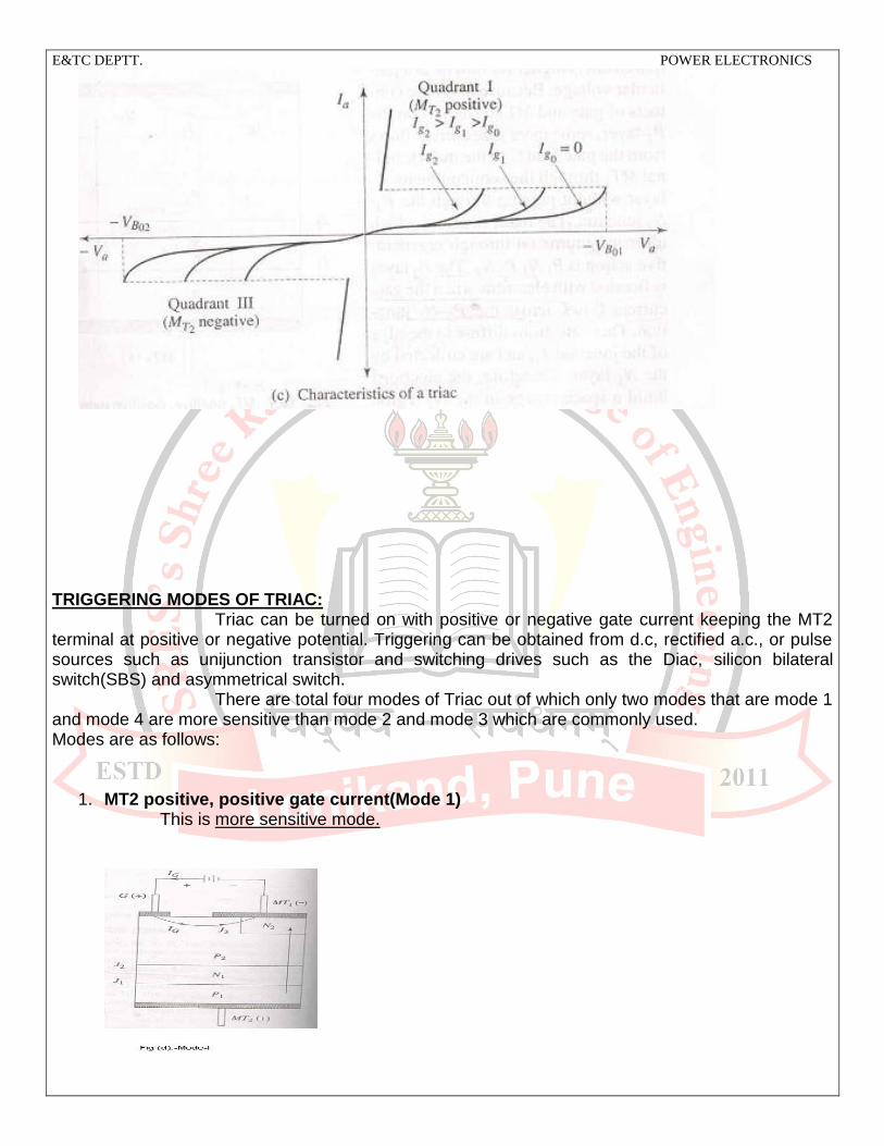
THEORY: A SCR has a reverse-blocking characteristics that prevents current flow in the cathode-to-anode direction. However, there are many applications, particularly in a.c. circuits, where the bi-directional conduction is required. Two thyristors may be connected in inverse-parallel, but at moderate power levels the two antiparallel thyristors can be integrated into single device structure, as shown in Fig(a). This device commonly known as Triac (triode a.c. switch) is represented by the circuit symbol shown in Fig(b). As the Triac can conduct in both the directions, the terms anode and cathode are not applicable to Triac. Its three terminals are usually designated as main terminals, MT1,MT2 and gate G, as in thyristor. The terminal MT1 is the reference point for measurement of voltages and currents at the gate terminal and at the terminal MT2. The gate is near to terminal MT1. The V-I characteristics of a Triac is shown in Fig(c). This characteristics of the Triac are based on the terminal MT1 as the reference point. The first quadrant is the region wherein MT2 is positive with respect to MT1 and vise-versa for the third quadrant. The peak voltage applied across the device in either direction must be less than the breakover voltage in order to retain control by the gate. A gate current of specified amplitude of either polarity will trigger a Triac into conduction in either quadrant, assuming that the device is in a blocking condition initially before the gate signal is applied. The characteristics of Triac are similar to SCR, both in blocking and conducting state, expect for fact that SCR conducts only in forward direction, Whereas the Triac conducts in both the direction.
Shree Ramchandra College of Engineering
Lonikand, Pune
Experiment No.
Name: Date of performance:
Class: Date of Submission:
Roll no: Signature:
E&TC DEPTT. POWER ELECTRONICS
Depending upon the polarity of gate pulse and biasing conditions, the main four layer structure that turns on by a regenerative process could be one of P1N1P2N2, P1N1P2N3, or P2N1P1N4.
E&TC DEPTT. POWER ELECTRONICS
TRIGGERING MODES OF TRIAC: Triac can be turned on with positive or negative gate current keeping the MT2 terminal at positive or negative potential. Triggering can be obtained from d.c, rectified a.c., or pulse sources such as unijunction transistor and switching drives such as the Diac, silicon bilateral switch(SBS) and asymmetrical switch. There are total four modes of Triac out of which only two modes that are mode 1 and mode 4 are more sensitive than mode 2 and mode 3 which are commonly used. Modes are as follows:
1. MT2 positive, positive gate current(Mode 1) This is more sensitive mode.
E&TC DEPTT. POWER ELECTRONICS
2. MT2 positive , negative gate current (Mode 2) ( Less sensitive ) 3. MT2 negative, positive gate current (Mode 3) ( less sensitive ) 4. MT2 negative, negative gate current(Mode 4): (more sensitive mode)
APPLICATIONS OF TRIAC:
1. Light dimmer, fan regulators. 2. Speed control of ac motor. 3. Musical light chaser. 4. Flashers 5. control of food mixers 6. for control of portable drilling machine
PROCEDURE: (A): Forward Characteristics: 9. Connect a VARIAC at zero position to given terminals on trainer kit. 10. Connect P to P & N to N, then Vg (+, -) to Vg (+, -) on kit. 11. Connect a 230V, 15W lamp as a load at given terminals. 12. Connect one ammeter for TRIAC current IT and another ammeter for gate current Ig at given
terminals. 13. This is MT2 (+ve), gate (+ve) mode of operation ( quadrant-I). 14. Ensuring that both VARIAC & Vg potentiometer are at 0 position, switch on the trainer kit &
VARIAC. 15. Now increase VARIAC voltage gradually to VS = 220V, then increase Ig gradually till load
activation (glowing of lamp laod) & measure load current (IT). Note these readings as Ig1= ---, VS1=220V, IT1= ---
16. Reset the system, Now keeping VS zero increase Ig2=Ig1+0.1 or 0.2mA and then increase VS gradually till TRIAC conduction. Note these readings as Ig2,VS2 & IT2.
17. Repeat the step7 for different values of gate currents Ig3,Ig4, etc. 18. Tabulate the readings and plot the IT verses VS. (quadrant – I)
E&TC DEPTT. POWER ELECTRONICS
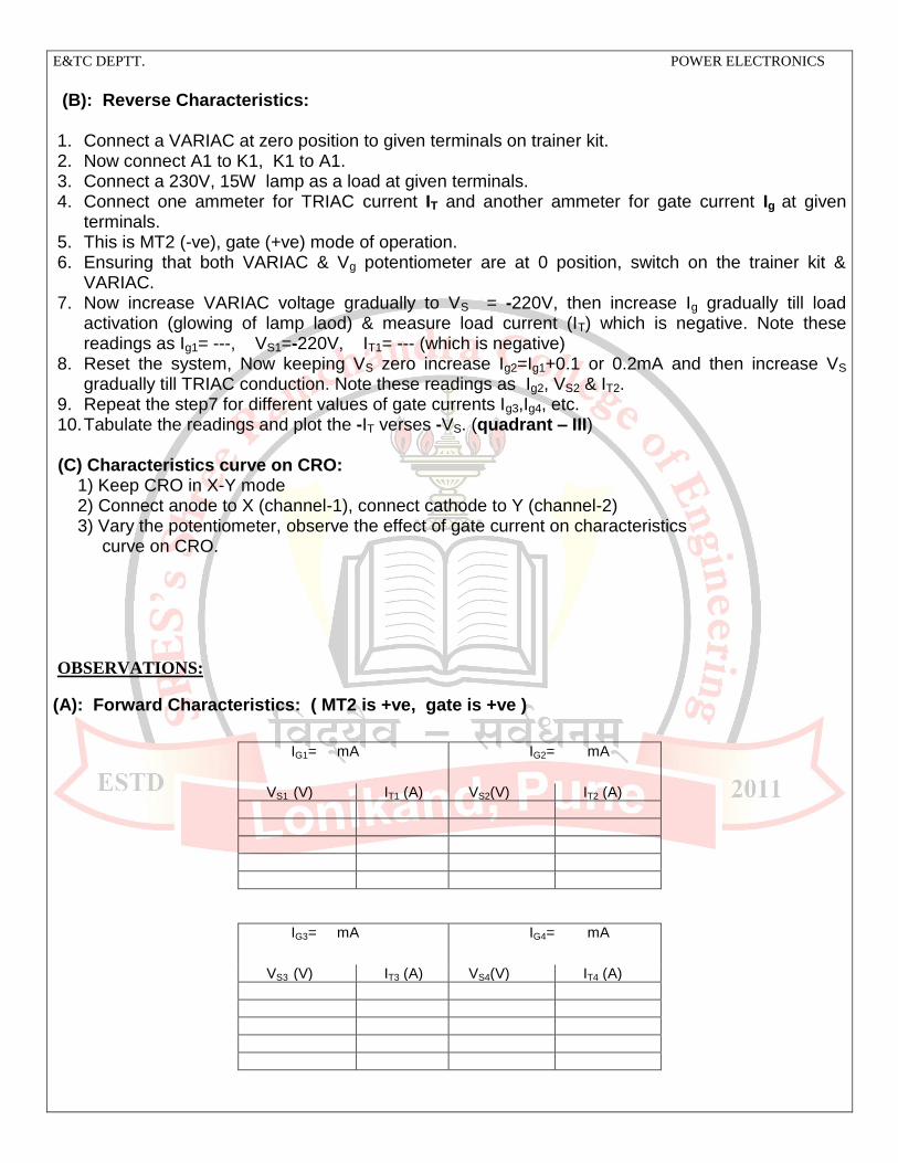
(B): Reverse Characteristics: 1. Connect a VARIAC at zero position to given terminals on trainer kit. 2. Now connect A1 to K1, K1 to A1. 3. Connect a 230V, 15W lamp as a load at given terminals. 4. Connect one ammeter for TRIAC current IT and another ammeter for gate current Ig at given
terminals. 5. This is MT2 (-ve), gate (+ve) mode of operation. 6. Ensuring that both VARIAC & Vg potentiometer are at 0 position, switch on the trainer kit &
VARIAC. 7. Now increase VARIAC voltage gradually to VS = -220V, then increase Ig gradually till load
activation (glowing of lamp laod) & measure load current (IT) which is negative. Note these readings as Ig1= ---, VS1=-220V, IT1= --- (which is negative)
8. Reset the system, Now keeping VS zero increase Ig2=Ig1+0.1 or 0.2mA and then increase VS gradually till TRIAC conduction. Note these readings as Ig2, VS2 & IT2.
9. Repeat the step7 for different values of gate currents Ig3,Ig4, etc. 10. Tabulate the readings and plot the -IT verses -VS. (quadrant – III)
(C) Characteristics curve on CRO: 1) Keep CRO in X-Y mode 2) Connect anode to X (channel-1), connect cathode to Y (channel-2) 3) Vary the potentiometer, observe the effect of gate current on characteristics curve on CRO.
OBSERVATIONS:
(A): Forward Characteristics: ( MT2 is +ve, gate is +ve )
IG1= mA IG2= mA
VS1 (V) IT1 (A) VS2(V) IT2 (A)
IG3= mA IG4= mA
VS3 (V) IT3 (A) VS4(V) IT4 (A)
E&TC DEPTT. POWER ELECTRONICS
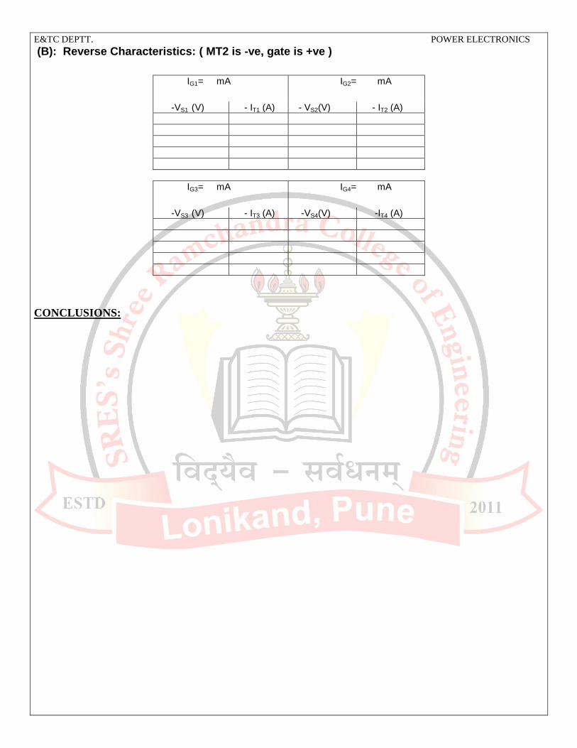
(B): Reverse Characteristics: ( MT2 is -ve, gate is +ve )
IG1= mA IG2= mA
-VS1 (V) - IT1 (A) - VS2(V) - IT2 (A)
IG3= mA IG4= mA
-VS3 (V) - IT3 (A) -VS4(V) -IT4 (A)
CONCLUSIONS:
E&TC DEPTT. POWER ELECTRONICS
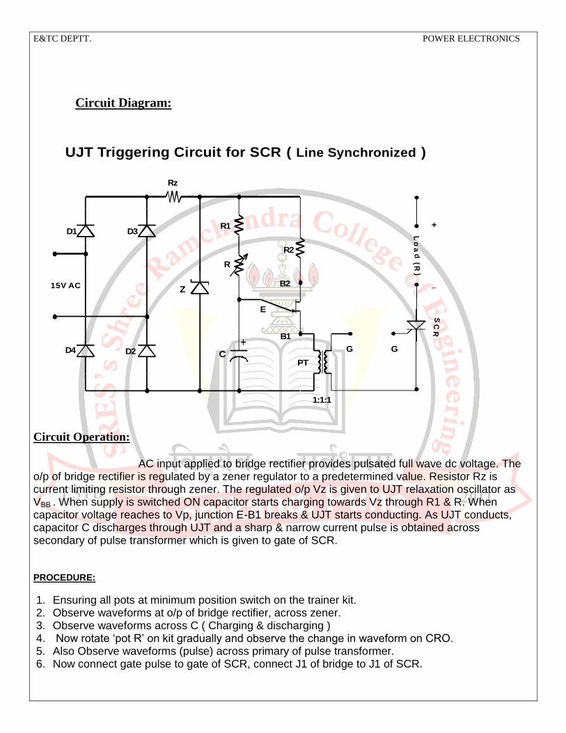
UJT Triggering Circuit for SCR
AIM: To study UJT Triggering Circuit for SCR APPRATUS:
1. Dual Trace SCR 2. Digital Multimeter 3. Trainer kit 4. Load resistors, Connectors, etc.
THEORY:
This training system is designed to explain working principles of UJT triggering circuit.UJT exhibits negative resistance characteristics hence it is operating under relaxation mode. Basically R & R-C triggering circuits provide long duration gate pulses which increases gate losses so that sharp & narrow pulses are preferred for SCR which can be obtained from UJT relaxation oscillator.Here a line synchronized UJT triggering circuit is used which consists of a bridge rectifier (without filter), a zener regulator & an UJT relaxation oscillator.
Shree Ramchandra College of Engineering
Lonikand, Pune
Experiment No.
Name: Date of performance:
Class: Date of Submission:
Roll no: Signature:
E&TC DEPTT. POWER ELECTRONICS
Circuit Diagram:
Lo
ad
(R
)
+
_
SC
R
PT
1:1:1
B1
B2
E
G G
D1
D2
D3
D4
R1
R
R2
Rz
Z
C
UJT Triggering Circuit for SCR ( )Line Synchronized
15V AC
Circuit Operation:
AC input applied to bridge rectifier provides pulsated full wave dc voltage. The o/p of bridge rectifier is regulated by a zener regulator to a predetermined value. Resistor Rz is current limiting resistor through zener. The regulated o/p Vz is given to UJT relaxation oscillator as VBB . When supply is switched ON capacitor starts charging towards Vz through R1 & R. When capacitor voltage reaches to Vp, junction E-B1 breaks & UJT starts conducting. As UJT conducts, capacitor C discharges through UJT and a sharp & narrow current pulse is obtained across secondary of pulse transformer which is given to gate of SCR. PROCEDURE:
1. Ensuring all pots at minimum position switch on the trainer kit. 2. Observe waveforms at o/p of bridge rectifier, across zener. 3. Observe waveforms across C ( Charging & discharging ) 4. Now rotate ‘pot R’ on kit gradually and observe the change in waveform on CRO. 5. Also Observe waveforms (pulse) across primary of pulse transformer. 6. Now connect gate pulse to gate of SCR, connect J1 of bridge to J1 of SCR.
E&TC DEPTT. POWER ELECTRONICS
7. Connect a load of 220 or 330, observe different waveforms across load by varying ‘pot R’ at different firing angles.
8. Also note down αmin & αmax 9. Sketch the waveforms across load & SCR at αmin & αmax 10. Tabulate the readings. OBSERVATION TABLE:
Sr. No.
Firing Angle
V0
1 αmax
2
3
4
5 αmin
CONCLUSIONS:
E&TC DEPTT. POWER ELECTRONICS
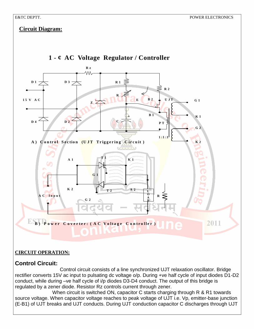
Single Phase AC Voltage Controller
AIM: To study single phase AC voltage controller for R load.
EQUIPMENTS & COMPONENTS:
1. Power scope / Dual trace CRO 2. Digital Multimeter 3. Trainer kit 4. 230V, 15W load lamp, Connectors, etc.
THEORY:
This training system is designed to explain working principle and method of obtaining the variable AC from fixed frequency AC supply.Here the Phase Angle Control technique is used using UJT triggering circuit.In order to control AC power we may use a Triac or SCRs connected in anti-parallel fashion. In our Trainer System we have used two SCRs in anti-parallel connection (full wave).The position of firing angle may be from 10o to 170o on half cycle to obtain maximum to minimum voltage across the load.As per power converter circuit, during + ve half cycle T2 becomes forward biased, after gating gate pulse T2 conducts in one direction and load voltage is positive. During –ve half cycle T1 becomes forward biased, after gating gate pulse T1 conducts in opposite direction and hence load voltage becomes negative. In this way by controlling firing angle AC voltage gets varied from fixed AC voltage.
Shree Ramchandra College of Engineering
Lonikand, Pune
Experiment No.
Name: Date of performance:
Class: Date of Submission:
Roll no: Signature:
E&TC DEPTT. POWER ELECTRONICS
Circuit Diagram:
1 - ¢ AC Voltage Regulator / Controller
B ) P o w e r C o v e r t e r : ( A C V o l t a g e C o n t r o l l e r )
LOAD
R
T 1
T 2
G 1
G 2
A 1
A 2
K 1
K 2
A C I n p u t
1 5 V A C
D 1
D 2
D 3
D 4
Z
R 1
R 2
R
C
B 1
B 2E U J T
1 : 1 : 1
P T
R z
A ) C o n tr o l S e c t io n (U J T T r ig g e r in g C ir c u it )
G 1
G 2
K 1
K 2
<
CIRCUIT OPERATION:
Control Circuit: Control circuit consists of a line synchronized UJT relaxation oscillator. Bridge rectifier converts 15V ac input to pulsating dc voltage o/p. During +ve half cycle of input diodes D1-D2 conduct, while during –ve half cycle of i/p diodes D3-D4 conduct. The output of this bridge is regulated by a zener diode. Resistor Rz controls current through zener. When circuit is switched ON, capacitor C starts charging through R & R1 towards source voltage. When capacitor voltage reaches to peak voltage of UJT i.e. Vp, emitter-base junction (E-B1) of UJT breaks and UJT conducts. During UJT conduction capacitor C discharges through UJT
E&TC DEPTT. POWER ELECTRONICS
and a pulse is obtained across primary of pulse transformer which is used as a gate pulse. Here R is a potentiometer which controls charging rate of capacitor. Pulse transformer has 1:1:1 turn ratio, therefore pulses of same rating will appear across both secondary windings. Pulse transformer also provides isolation between triggering circuit & power converter circuit. Pulses at first secondary are given to SCR T1 as G1-K1, similarly Pulses at next secondary are given to SCR T2 as G2-K2.
which reduces the gate losses. 2. It provides isolation between triggering circuit & power circuit. 3. Firing angle range is 0 - 1800 4. It exhibits –ve resistance characteristics hence used under relaxation Mode.
Power Converter Circuit: Power converter circuit consists of two SCRs connected in anti-parallel configuration. During + ve half cycle of ac input T2 becomes forward biased, after gating gate pulse T2 conducts in one direction and load voltage is positive. During –ve half cycle T1 becomes forward biased, after gating gate pulse T1 conducts in opposite direction and hence load voltage becomes negative. In this way by controlling firing angle by pot R in control circuit, output AC voltage gets varied from fixed input AC voltage.
PROCEDURE:
1. Observe & sketch different waveforms in control circuit i.e. o/p of bridge, voltage across zener, voltage across capacitor C and voltage across primary of pulse transformer.
2. Now connect G1 of control circuit to G1 of power converter, similarly connect K1 to K1, G2 to G2 & K2 to K2.
3. Connect a lamp load of 15W / 25W / 40W in given bulb socket. 4. AC input (36V ac rms) is connected internally. 5. Connect a CRO & a multimeter across the load. 6. Observe load voltage waveform on CRO, measure corresponding o/p voltage & firing angle. 7. Now vary the firing angle by pot, observe different waveforms across load, measure
corresponding o/p voltages & firing angles. 8. Tabulate the readings, compare with theoretical o/p, plot the graph α vs Vo
E&TC DEPTT. POWER ELECTRONICS
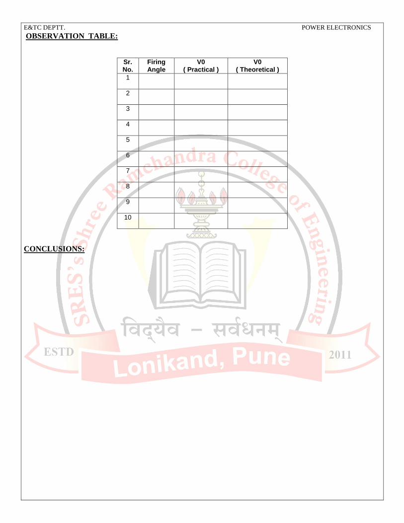
OBSERVATION TABLE:
Sr. No.
Firing Angle
V0 ( Practical )
V0 ( Theoretical )
1
2
3
4
5
6
7
8
9
10
CONCLUSIONS:
E&TC DEPTT. POWER ELECTRONICS
Single Phase Half controlled Rectifier (Semiconverter)
AIM: To study Single Phase Half controlled Rectifier (Semi converter) for R . APPRATUS: 1. Dual Trace CRO 2. Digital Multimeter 3. Trainer kit 4. Load lamp, Connectors, etc.
THEORY: This training system is designed to explain working principle of semiconverter.Here the Phase Angle Control technique is used using UJT triggering circuit.The position of firing angle may be from 10o to 170o on half cycle to obtain maximum to minimum voltage across the load. During + ve half cycle T1 & D2 become forward biased, after gating gate pulse T1 & D2 conduct in one direction and load voltage is positive. During –ve half cycle T2 & D1 become forward biased, after gating gate pulse T2 & D1 conduct in the same direction and hence load voltage remains positive. In this way by controlling firing angle dc voltage gets controlled.During firing angle duration there is inherent freewheeling by either T1-D1 or T2-D2.
Shree Ramchandra College of Engineering
Lonikand, Pune
Experiment No.
Name: Date of performance:
Class: Date of Submission:
Roll no: Signature:
E&TC DEPTT. POWER ELECTRONICS
CIRCUIT OPERATION:
Control Circuit: Control circuit consists of a line synchronized UJT relaxation oscillator. Bridge rectifier converts 15V ac input to pulsating dc voltage o/p. During +ve half cycle of input diodes D1-D2 conduct, while during –ve half cycle of i/p diodes D3-D4 conduct. The output of this bridge is regulated by a zener diode. Resistor Rz controls current through zener. When circuit is switched ON, capacitor C starts charging through R & R1 towards source voltage. When capacitor voltage reaches to peak voltage of UJT i.e. Vp, emitter-base junction (E-B1) of UJT breaks and UJT conducts. During UJT conduction capacitor C discharges through UJT and a pulse is obtained across primary of pulse transformer which is used as a gate pulse. Here R is a potentiometer which controls charging rate of capacitor. Pulse transformer has 1:1:1 turn ratio, therefore pulses of same rating will appear across both secondary windings. Pulse transformer also provides isolation between triggering circuit & power converter circuit. Pulses at first secondary are given to SCR T1 as G1-K1, similarly Pulses at next secondary are given to SCR T2 as G2-K2. Advantages: 1. UJT triggering circuit provides sharp & narrow gate pulses which reduces the gate losses. 2. It provides isolation between triggering circuit & power circuit. 3. Firing angle range is 0 - 1800 4. It exhibits –ve resistance characteristics hence used under relaxation Mode.
Power Converter Circuit: Power converter circuit consists of two SCRs & two diodes connected in symmetrical configuration. During + ve half cycle T1 & D2 become forward biased, after gating gate pulse to T1, both T1 & D2 conduct in one direction and load voltage is positive. During –ve half cycle T2 & D1 become forward biased, after gating gate pulse to T2, both T2 & D1 conduct in the same direction and hence load voltage remains positive. In this way by controlling firing angle by pot R in control circuit dc voltage gets controlled. During firing angle duration there is inherent freewheeling by either T1-D1 or T2-D2 when R-L load is connected.
E&TC DEPTT. POWER ELECTRONICS
PROCEDURE:
1. Observe & sketch different waveforms in control circuit i.e. o/p of bridge, voltage across zener, voltage across capacitor C and voltage across primary of pulse transformer.
2. Now connect G1 of control circuit to G1 of power converter, similarly connect K1 to K1, G2 to G2 & K2 to K2.
3. Connect a lamp load ( R load )of 15W / 25W / 40W in given bulb socket. 4. Connect a CRO & a multimeter across the load. 5. Observe load voltage waveform on CRO, measure corresponding o/p voltage & firing angle. 6. Now vary the firing angle by pot, observe different waveforms across load, measure
corresponding o/p voltages & firing angles. 7. Tabulate the readings, compare with theoretical o/p, plot the graph α vs Vo 8. Repeat the all procedure for R – L load.
OBSERVATION TABLE:
1) For R load:-
Sr. No.
Firing Angle
V0 ( Practical )
V0 ( Theoretical )
1
2
3
4
5
6
7
CONCLUSIONS:
E&TC DEPTT. POWER ELECTRONICS
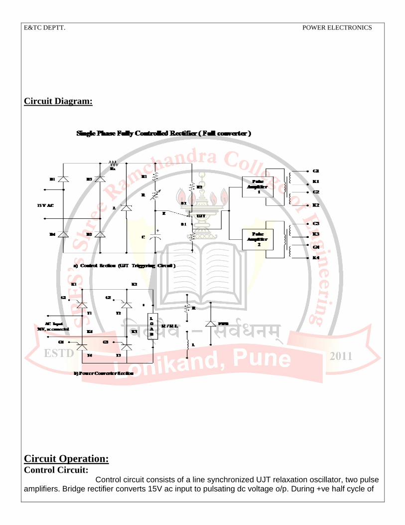
Single Phase Fully controlled Rectifier (Fullconverter)
AIM: To study Single Phase fully controlled Rectifier (Full converter)
for R & R-L load.
APPRATUS: 1. Dual Trace CRO 2. Digital Multimeter 3. Trainer kit 4. Load lamp, Connectors, etc.
THEORY: This training system is designed to explain working principle of Full converter. Here the Phase Angle Control technique is used using UJT triggering circuit.The position of firing angle may be from 18o to 170o on half cycle to obtain maximum to minimum voltage across the load. During + ve half cycle T1 & T3 become forward biased, after gating gate pulse T1 & T3 conduct in one direction and load voltage is positive. During –ve half cycle T2 & D1 become forward biased, after gating gate pulse T2 & T4 conduct in the same direction and hence load voltage remains positive. In this way by controlling firing angle dc voltage gets controlled.
Shree Ramchandra College of Engineering
Lonikand, Pune
Experiment No.
Name: Date of performance:
Class: Date of Submission:
Roll no: Signature:
E&TC DEPTT. POWER ELECTRONICS
Circuit Diagram:
Circuit Operation: Control Circuit: Control circuit consists of a line synchronized UJT relaxation oscillator, two pulse amplifiers. Bridge rectifier converts 15V ac input to pulsating dc voltage o/p. During +ve half cycle of
E&TC DEPTT. POWER ELECTRONICS
input diodes D1-D2 conduct, while during –ve half cycle of i/p diodes D3-D4 conduct. The output of this bridge is regulated by a zener diode. Resistor Rz controls current through zener. When circuit is switched ON, capacitor C starts charging through R & R1 towards source voltage. When capacitor voltage reaches to peak voltage of UJT i.e. Vp, emitter-base junction (E-B1) of UJT breaks and UJT conducts. During UJT conduction capacitor C discharges through UJT and a pulse is obtained across primary of pulse transformer which is used as a gate pulse. Here R is a potentiometer which controls charging rate of capacitor. Pulse transformer has 1:1:1 turn ratio, therefore pulses of same rating will appear across both secondary windings. Pulse transformer also provides isolation between triggering circuit & power converter circuit. Pulses at first secondary are given to SCR T1 as G1-K1, similarly Pulses at next secondary are given to SCR T2 as G3-K3. Gates & cathodes of T2 & T4 are connected internally. Advantages:
1. UJT triggering circuit provides sharp & narrow gate pulses which reduces the gate losses. 2. It provides isolation between triggering circuit & power circuit. 3. Firing angle range is 0 - 1800 4. It exhibits –ve resistance characteristics hence used under relaxation Mode.
Power Converter Circuit: Power converter circuit consists of four SCRs connected in bridge configuration. During + ve half cycle T1 & T2 become forward biased, after gating gate pulse, both T1 & T2 conduct in one direction and load voltage is positive. During –ve half cycle T3 & T4 become forward biased, after gating gate pulse, both T3 & T4 conduct in the same direction and hence load voltage remains positive. In this way by controlling firing angle by pot R in control circuit dc voltage gets controlled. For an inductive load a reverse voltage [-L(di/dt)] appears across load during firing angle duration.
Circuit Diagram:
E&TC DEPTT. POWER ELECTRONICS
PROCEDURE:
19. Observe & sketch different waveforms in control circuit i.e. o/p of bridge, voltage across zener, voltage across capacitor C and voltage across primary of pulse transformer.
20. Now connect G1 of control circuit to G1 of power converter, similarly connect K1 to K1, G2 to G2 & K2 to K2, G3 to G3 & K3 to K3, G4 to G4 & K4 to K4
21. Connect a lamp load ( R load )of 15W / 25W / 40W in given bulb socket. 22. Connect a CRO & a multimeter across the load. 23. Observe load voltage waveform on CRO, measure corresponding o/p voltage & firing angle. 24. Now vary the firing angle by pot, observe different waveforms across load, measure
corresponding o/p voltages & firing angles. 25. Tabulate the readings, compare with theoretical o/p, plot the graph α vs Vo 26. Repeat the all procedure for R – L load.
Specifications:
E&TC DEPTT. POWER ELECTRONICS
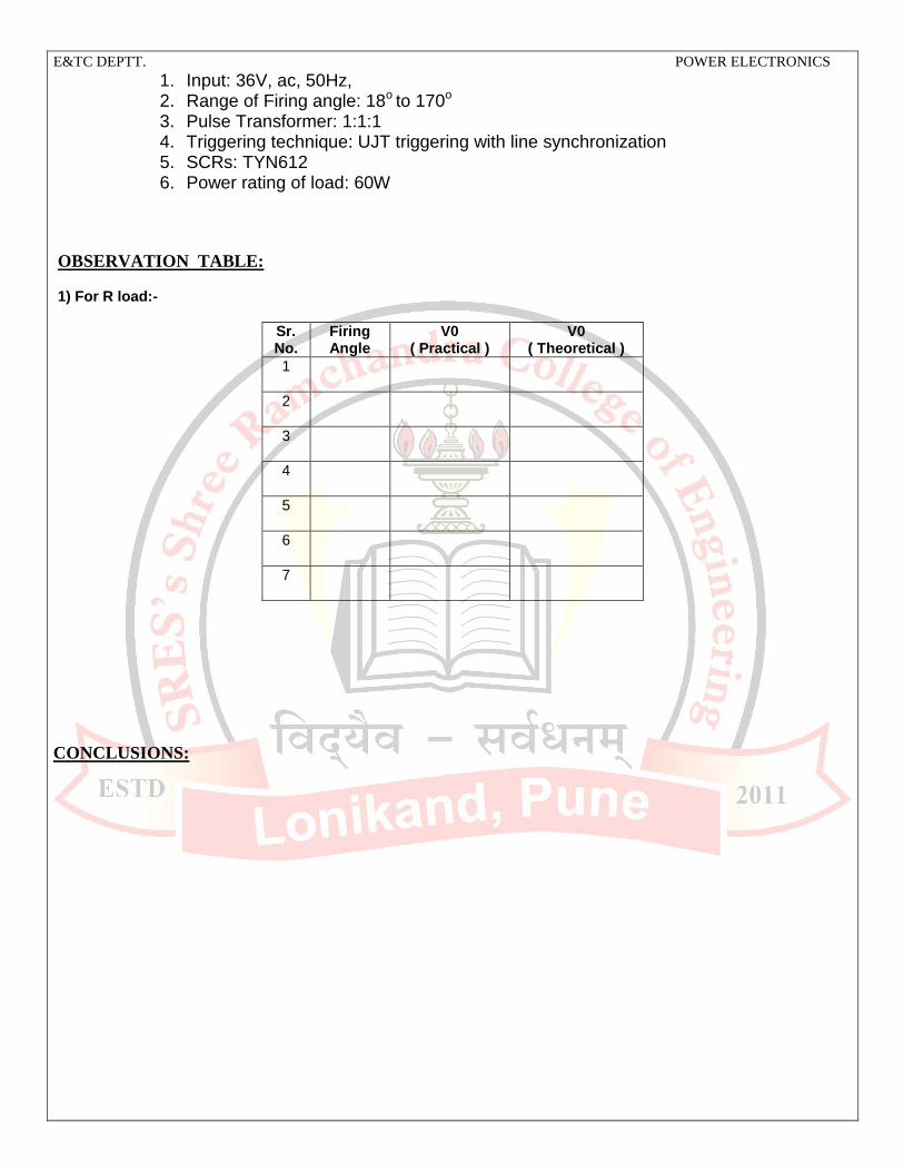
1. Input: 36V, ac, 50Hz, 2. Range of Firing angle: 18o to 170o 3. Pulse Transformer: 1:1:1 4. Triggering technique: UJT triggering with line synchronization 5. SCRs: TYN612 6. Power rating of load: 60W
OBSERVATION TABLE: 1) For R load:-
Sr. No.
Firing Angle
V0 ( Practical )
V0 ( Theoretical )
1
2
3
4
5
6
7
CONCLUSIONS:
E&TC DEPTT. POWER ELECTRONICS
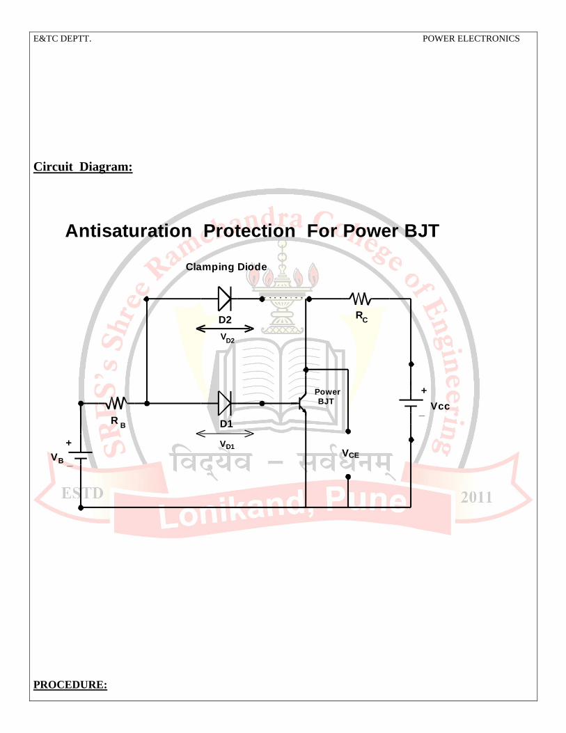
Antisaturation protection control for power BJT
AIM: To study working principle of Antisaturation protection control for power BJT
APPRATUS: 1. Trainer kit 2. Digital Multimeter 3. Dual power supply 4. Connectors, etc
THEORY: Antisaturation control circuit consists of a collector clamping diode. This control is
used to operate BJT in soft saturation instead of hard saturation. If BJT is operated in hard saturation,
storage time increases which reduces switching speed. Hence to increase switching speed of power
BJT it is preferred to operate BJT in soft saturation which can be accomplished by ‘antisaturation
control. In the circuit when clamping diode is not connected to the collector, BJT operates in hard
saturation and VCE(sat) =< 0.7V. When clamping diode is connected to collector, VCE(clamp) > 0.7V i.e.
VCE(sat). For clamping VD1 > VD2. Finally the clamping action results in reduction of storage time, hence
increase in switching speed.
Shree Ramchandra College of Engineering
Lonikand, Pune
Experiment No.
Name: Date of performance:
Class: Date of Submission:
Roll no: Signature:
E&TC DEPTT. POWER ELECTRONICS
Circuit Diagram:
D1
D2
RB
CR
Vcc
VCEBV
Clamping Diode
Antisaturation Protection For Power BJT
+
+
_
_
PowerBJT
VD1
VD2
PROCEDURE:
E&TC DEPTT. POWER ELECTRONICS
1. Apply Vcc = 10V, VBB = 0V, measure VCE
2. Now increase VB till VCE = < 0.7V, measure this VCE as VCE(sat)
3. Connect D2 to collector of transistor, measure again VCE(clamp) and compare with VCE(sat).
4. Result should be VCE(clamp) > VCE(sat) which shows that BJT is not working in hard saturation but
working in soft saturation.
5. Again remove connection of D2 from collector, measure VCE , it will be again VCE(sat) =< 0.7V.
6. Also ensure that VD1 > VD2 under clamping action.
AIM: To study DC Chopper (step down) using MOSFET. APPRATUS: 1. Dual trace CRO
2. Digital Multimeter
3. Trainer kit
4. Power supply,
5. Connectors, etc.
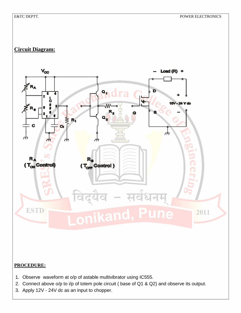
THEORY:
This training system is designed to explain working principle of step down DC chopper. A
chopper is a circuit which converts fixed dc voltage into Variable dc voltage i.e. dc – dc converter.
It consists of a gate drive circuit & a MOSFET as a switch. By making switch ON / OFF o/p voltage
is made variable form 0 – Vs Here the time ratio Control (TRC) technique is used using a IC555
based gate drive circuit.The ON time can be varied by RA, OFF time can be varied by RB, hence
duty cycle / frequency can be change.
Shree Ramchandra College of Engineering
Lonikand, Pune
Experiment No.
Name: Date of performance:
Class: Date of Submission:
Roll no: Signature:
E&TC DEPTT. POWER ELECTRONICS
Circuit Diagram:
PROCEDURE:
1. Observe waveform at o/p of astable multivibrator using IC555.
2. Connect above o/p to i/p of totem pole circuit ( base of Q1 & Q2) and observe its output.
3. Apply 12V - 24V dc as an input to chopper.
E&TC DEPTT. POWER ELECTRONICS
4. Now connect o/p of totem pole to gate of MOSFET.
5. Connect a CRO across load which is internally connected.
6. Observe load voltage waveform on CRO, measure TON, TOFF on CRO and measure
corresponding o/p voltage.
7. Now vary the TON or TOFF by RA or RB respectively and measure corresponding output voltages.
8. Tabulate the readings, compare with theoretical o/p.
OBSERVATION TABLE:
Sr.
No.
TON TOFF T Duty
cycle
V0
( Practical )
V0
(Theoretical )
1
2
3
4
5
6
7
8
9
10
CONCLUSIONS:
E&TC DEPTT. POWER ELECTRONICS
Switch Mode Power Supply (SMPS)
AIM: To study working principle of Switch Mode Power Supply (SMPS) APPRATUS:
1. Trainer kit 2. Digital Multimeter 3. VARIAC 4. Connectors, etc.
THEORY:
This training system is designed to explain working principle of Switch Mode Power Supply (SMPS)TOP-Switch is a single CMOS chip which integrates a power MOSFET, PWM control & protection circuitry on a single chip.This design delivers 10W at 12V. It is operated from 120V – 265V ac supply.
Pin Functional Description: DRAIN (D) Pin:
High voltage power MOSFET drain output. The internal startup bias current is drawn from this pin through a switched high voltage current source. Internal current limit sense point for drain current. CONTROL (C) Pin: Error amplifier and feedback current input pin for duty cycle control. Internal shunt regulator connection to provide internal bias current during normal operation. It is also used as the connection point for the supply bypass and auto-restart/ compensation capacitor.
LINE-SENSE (L) Pin: (Y or R package only) Input pin for OV, UV, line feed forward with DCMAX reduction, remote ON/OFF and synchronization. A connection to SOURCE pin disables all functions on this pin.
EXTERNAL CURRENT LIMIT (X) Pin: (Y or R package only)
Shree Ramchandra College of Engineering
Lonikand, Pune
Experiment No.
Name: Date of performance:
Class: Date of Submission:
Roll no: Signature:
E&TC DEPTT. POWER ELECTRONICS
Input pin for external current limit adjustment, remote ON/OFF, and synchronization. A connection to SOURCE pin disables all functions on this pin.
MULTI-FUNCTION (M) Pin: (P or G package only) This pin combines the functions of the LINE-SENSE (L) and EXTERNAL CURRENT LIMIT (X) pins of the Y package into one pin. Input pin for OV, UV, line feed forward with DCMAX reduction, external current limit adjustment, remote ON/OFF and synchronization. A connection to SOURCE pin disables allfunctions on this pin and makes TOPSwitch-GX operate in simple three terminal mode (like TOPSwitch-II).
FREQUENCY (F) Pin: (Y or R package only)
Input pin for selecting switching frequency: 132 kHz if connected to SOURCE pin and 66 kHz if connected to CONTROL pin. The switching frequency is internally set for fixed 132 kHz operation in P and G packages. SOURCE (S) Pin:
Output MOSFET source connection for high voltage power return. Primary side control circuit common and reference point.
Circuit Diagram of SMPS:
E&TC DEPTT. POWER ELECTRONICS
PROCEDURE: (A) For Load Regulation:
1. Connect VARIAC to ac input terminals, ensuring at zero position switch ON it. 2. Now apply 230V ac from VARIAC, measure o/p at given terminals, it will be of 12V dc which is
no load voltage i.e. VNL = 12V. 3. Connect a load or (rheostat) having 100Ω to 200Ω at o/p, measure o/p across load. 4. Vary the load, from 220Ω to 2,2KΩ measure corresponding load voltages. 5. Tabulate the readings, find load regulation.
VNL- VFL
%Load Regulation = -------------- * 100 VFL
(B) For Line Regulation:
1. Connect VARIAC to ac input terminals, ensuring at zero position switch ON it. 2. Now apply 250V ac from VARIAC, measure o/p at given terminals, it will be of 12V dc. 3. Decrease the ac i/p from VARIAC in step of 10V, measure o/p. 4. Repeat step 3 for various i/p voltages up to 150V. 5. Tabulate the readings, find line regulation.