US 20120212854A1 (19) United States (12) Patent Application Publication (10) Pub. N0.: US 2012/0212854 A1 Golcher et al. (43) Pub. Date: Aug. 23, 2012 (54) SHUNT FOR MAGNETORESISTIVE Publication Classi?cation TRANSDUCER HEADS FOR (51) Int Cl EII£¥EE¥ISS§TIC DISCHARGE G11B 5/40 (2006.01) G11B 5/39 (2006.01) (75) Inventors: Peter J. Golcher, Los Gatos, CA H05K 13/00 (2006-01) (US); Icko E.T. Iben, Santa Clara, GHB 21/02 (2006-01) CA (U S); Ho-Yiu Lam, Mountain VleW, CA (Us); J0“ Luis A- (52) us. Cl. ...... .. 360/75; 360/128; 360/323; 29/60307; salenga, San Jose’ CA (Us) G9B/5.143; G9B/21.003; G9B/5.113 (73) Assignee: International Business Machines Corporation, Armonk, NY (U S) (57) ABSTRACT (21) Appl. N0.: 13/463,732 ma netoresistive trans ucer ea assem me u es a _ A g ' ' d h d bly ' 1 d (22) Flled? May 31 2012 reader element, a Writer element and a high impedance shunt . . electrically connecting the reader element and the Writer ele Related U's' Apphcatlon Data ment. The high impedance shunt provides a high impedance (63) Continuation of application No, 12/015,438, ?led on conductive path for maintaining electrostatic charge equipo Jan. 16, 2008, noW Pat. No. 8,199,444. tential between the reader element and the Writer element.
Transcript
US 20120212854A1
(19) United States (12) Patent Application Publication (10) Pub. N0.: US 2012/0212854 A1
Golcher et al. (43) Pub. Date: Aug. 23, 2012
(54) SHUNT FOR MAGNETORESISTIVE Publication Classi?cation TRANSDUCER HEADS FOR (51) Int Cl
(75) Inventors: Peter J. Golcher, Los Gatos, CA H05K 13/00 (2006-01) (US); Icko E.T. Iben, Santa Clara, GHB 21/02 (2006-01) CA (U S); Ho-Yiu Lam, Mountain VleW, CA (Us); J0“ Luis A- (52) us. Cl. ...... .. 360/75; 360/128; 360/323; 29/60307; salenga, San Jose’ CA (Us) G9B/5.143; G9B/21.003; G9B/5.113
(73) Assignee: International Business Machines Corporation, Armonk, NY (U S)
(57) ABSTRACT (21) Appl. N0.: 13/463,732
ma netoresistive trans ucer ea assem me u es a _ A g ' ' d h d bly ' 1 d
(22) Flled? May 31 2012 reader element, a Writer element and a high impedance shunt . . electrically connecting the reader element and the Writer ele
Related U's' Apphcatlon Data ment. The high impedance shunt provides a high impedance (63) Continuation of application No, 12/015,438, ?led on conductive path for maintaining electrostatic charge equipo
Jan. 16, 2008, noW Pat. No. 8,199,444. tential between the reader element and the Writer element.
Patent Application Publication Aug. 23, 2012 Sheet 1 0f 9 US 2012/0212854 A1
1 0
FIG. 1A (PRIOR ART)
Patent Application Publication Aug. 23, 2012 Sheet 2 0f 9 US 2012/0212854 A1
10'\
1i 14_A
146
\_> 14_B
12_A
E /12
12_B
FIG. 1B (PRIOR ART)
Patent Application Publication Aug. 23, 2012 Sheet 3 0f 9 US 2012/0212854 A1
\- Charge on insulator surface
20\
Charge on metal leadsurface
A’ _ _ _ _
25/ 26--'_/_\ _ _ _ _ Uniform charge within
metal lead
22\ lead
FIG. 2 (PRIOR ART)
Patent Application Publication Aug. 23, 2012 Sheet 5 0f 9 US 2012/0212854 A1
a/
A m.----w.w_.nm..---.m m BmEoO m “ EEEXm "l l- .
n. ............ ..n / / / /
/ / / / ow Nw #m @w
Patent Application Publication Aug. 23, 2012 Sheet 6 0f 9 US 2012/0212854 A1
FIG. 5
Patent Application Publication Aug. 23, 2012 Sheet 7 0f 9 US 2012/0212854 A1
60" Ground / External Device
34
Q
Patent Application Publication Aug. 23, 2012 Sheet 8 0f 9 US 2012/0212854 A1
Ground /
65x External Device 34
20
Q
m
22 _~ : ".‘.-_-:_-'. '._-:-_
44 22 44
Patent Application Publication Aug. 23, 2012 Sheet 9 0f 9 US 2012/0212854 A1
72 74
77
/78
FIG. 7
US 2012/0212854 A1
SHUNT FOR MAGNETORESISTIVE TRANSDUCER HEADS FOR
ELECTROSTATIC DISCHARGE PROTECTION
CROSS-REFERENCE TO RELATED APPLICATIONS
[0001] This patent application is a continuation patent application of US. patent application Ser. No. 12/015,438, ?led on J an. 16, 2008, the disclosure of Which is incorporated herein its entirety by reference.
BACKGROUND
[0002] 1. Field of the Invention [0003] The present invention relates to magnetoresistive (MR) heads, and more particularly to protecting MR heads from electrostatic discharge (ESD). [0004] 2. Background Information [0005] In magnetic data storage devices, such as those used for tape or hard disk drives (HDD), transducer heads are utiliZed for reading and Writing data on magnetic media. Such transducer heads typically include transducer elements for reading (readers) and Writing (Writers) magnetic information on magnetic media. The transducer elements are typically small in siZe and are deposited on a Wafer using lithographic techniques. [0006] The readers include magnetoresistive (MR) sensors comprising thin ?lm sheet resistors that are highly susceptible to damage from electrostatic discharge, (ESD), either through Joule heating from high currents or from dielectric break doWn. The Writers are inductive, and alone are much less susceptible to ESD damage from high currents because they are built to sustain high Writer currents. HoWever, as shoWn by an example in FIG. 1A, a typical HDD or tape MR transducer head 10 comprises a piggyback structure, Wherein compo nents of each reader 12 and Writer 14 are separated by one or more relatively thin insulation layers such as oxide layers 16. The reader 12 and Writer 14 are encapsulated by a substrate 18 and a closure 19. The Writer 14 is stacked on top of the reader 12 vertically in thin ?lm layers. Referring noW also to a schematic vieW of the MR transducer head 10 in FIG. 1B, a reader 12 includes shields 12A-B and a read sensor 12C disposed therebetWeen. A Writer 14 includes Writer poles 14A-B separated by a Writer gap 14C. Further, leads 22 pro vide conductive paths to the reader 12 and the Writer 14. [0007] The insulation layers betWeen the readers and Writ ers are susceptible to dielectric breakdoWn With damaging electric ?eld levels on the order of 1><108 to 2><108 V/m. One speci?c failure mode that takes place in the piggyback struc tured MR as in FIG. 1 is shorting betWeen the reader 12 and Writer 14 Within the same transducer element 10. For an insulation layer thickness of 0.6 microns, a voltage differen tial of 60-120 V Will result in dielectric breakdoWn leading to ESD failure and resulting damage. [0008] ESD damage is a detractor for production yield dur ing the transducer head manufacturing process. ESD damage can manifest in MR sensor resistance value as over high limit (OHL), as under loW limit resistance (U LL) measurement and any value in-betWeen. Subtle ESD damage can also be mag netic in nature and may not be readily observable as a change in resistance. The likelihood of shorting events betWeen read ers and Writers due to ESD can be as high as the typical OHL failure mode. Extant tape heads contain upWards of 30 to 40
Aug. 23, 2012
reader-Writer pairs per tape head, such that a per-transducer loss as loW as 0.1% translates to a large loss of3 to 4% loss of tape heads. [0009] Referring to FIG. 2, in tape head manufacturing, a ?exible cable 20, Which is made of an insulating material, such as Kapton (polyimide), is bonded to the tape head mod ule to provide current passage to all the readers and Writers via metal leads 22. The leads 22 are connected to the readers/ Writers and are sandWiched betWeen insulating Kapton layers to provide proper electrical insulation betWeen the leads for mechanical structure and to prevent electrical shorting betWeen the leads. Similar ?exible cables are also being used in HDD head manufacturing. [0010] The Kapton cable surface may collect electrostatic charge through tribocharging due to handling or repeatedly sliding betWeen ?xtures. In this example, an electrostatic charge is shoWn as a negative charge 24 Which induces a positive charge 25 on the surface of the metal leads 22. A uniform distribution of a negative charge 26 remains in the bulk of the metal lead 22, sustaining conservation of charge, and thus, maintaining charge neutrality. HoWever, because Kapton is made of insulating material, tribocharging on the Kapton surface is localiZed and results in uneven surface charge distribution. As a result, the charge induced on the leads 22 varies With the amount of localiZation on the Kapton surface. This variation in charge induced on the leads 22 causes a potential difference betWeen the leads 22. Once such potential difference exceeds the dielectric breakdoWn thresh old of the insulation layer 16 (FIG. 1) betWeen the readers 12 and Writers 14, electrostatic discharge betWeen the leads dam ages the tape head. The same occurs for HDD heads.
BRIEF SUMMARY
[0011] High impedance electrical shunts are utiliZed to pro vide electrostatic discharge protection for heads containing magnetoresistive transducer elements and inductive Writers. In one embodiment, a magnetoresistive transducer head assembly according to the present invention comprises a reader element, a Writer element, and a high impedance shunt electrically connecting the reader element and the Writer ele ment. The high impedance shunt provides a high impedance conductive path for maintaining electrostatic charge equipo tential betWeen the reader element and the Writer element While they are un-poWered. When the leads are connected to a common electrical ground point, the uniform distribution of negative charge in the leads dissipates to equalize the lead potential. [0012] In one implementation, the reader element com prises a magnetoresistive (MR) sensor element and the Writer element comprises an inductive element, and the reader ele ment and the Writer element are assembled as a piggyback structure, such that the Writer element is physically located on-top of the reader element, and the reader electrical con tacts are separated from the Writer electrical contacts by a thin insulation layer. [0013] Preferably, a high impedance shunt has an imped ance value that alloWs read/Write signal measurements via the reader and Writer elements for normal read/Write operations With the transducer heads, With the high impedance shunt in place. In one example, for device resistances betWeen about 109 and 4009, and assuming that an acceptable leakage current through the shunt resistors is 0.1% of the current through the device, then the high impedance shunt can have a resistance value betWeen about 10 k9 and 400 kQ.
US 2012/0212854 A1
[0014] In another embodiment, a magnetoresistive trans ducer head assembly comprises plural reader elements, plural Writer elements and plural high impedance shunts electrically connecting the reader elements and the Writer elements. The high impedance shunts provide high impedance conductive paths for maintaining common voltage betWeen the reader elements and the Writer elements to reduce electrostatic dis charge betWeen the reader and Writer elements. The high impedance shunts provide high impedance conductive paths for maintaining electrostatic charge equipotential betWeen the reader elements and the Writer elements, While alloWing normal operation of the reader elements and the Writer ele ments. In one implementation, at least one Writer element lead is connected to a high impedance shunt, and at least one reader element lead is connected to a high impedance shunt, and the shunts Which connect the at least one Writer and the at least one reader, are connected to a common contact point. [0015] The magnetoresistive (MR) transducer head assem bly may further comprise a substrate on Which the reader and Writer elements are deposited, Wherein the high impedance shunts are deposited on the same substrate. The high imped ance shunts may instead be deposited on a separate substrate that is bonded to said transducer substrate. The high imped ance shunts may also be deposited on a Wafer substrate Which is fabricated into a ?ip chip. The ?ip chip is then bonded to a cable Which is connected to the transducers and Which pro vides read/Write signals to the transducer head assembly. The high impedance shunts may comprise high impedance thin ?lm resistive elements, tunnel junction resistors, a high impedance bus, etc. [0016] The aspects and advantages of the above mentioned features, along With additional features Which are embodied in the invention Will become understood With reference to the folloWing descriptions, appended claims, and accompanying ?gures.
BRIEF DESCRIPTION OF THE SEVERAL VIEWS OF THE DRAWINGS
[0017] FIG. 1A shoWs a conventional MR transducer head assembly With a piggyback structure; [0018] FIG. 1B shoWs a schematic vieW of the MR trans ducer head assembly With a piggyback structure of FIG. 1A; [0019] FIG. 2 shoWs a schematic of electrostatic charges on a cable and on metal leads for transducer elements of a con ventional MR transducer head; [0020] FIG. 3 shoWs an example shunt circuit of discrete high impedance shunts for an MR transducer head assembly, according to an embodiment of the present invention; [0021] FIG. 4 shoWs an example shunt circuit of a high impedance bus bar shunt for an MR transducer head assem bly, according to an embodiment of the present invention; [0022] FIG. 5 shoWs another example shunt circuit of a high impedance bus bar shunt for an MR transducer head assem bly, according to an embodiment of the present invention; [0023] FIGS. 6A and 6B shoW example placements of the high impedance shunts; and [0024] FIG. 7 illustrates an example tape drive Which may be employed in the context of the present invention.
DETAILED DESCRIPTION
[0025] Shunts for magnetoresistive (MR) heads, including readers and Writers, for protecting against electrostatic dis charge betWeen readers and Writers therein are provided. In
Aug. 23, 2012
one embodiment of the invention, a shunt comprises a high impedance (high resistance) shunt that reduces the occur rence of electrostatic discharge in MR heads by equalizing the relative charge potential betWeen the readers and Writers in an MR head When electrically un-poWered (i.e., not coupled to an electrical poWer source). The high impedance shunt pro vides a high impedance conductive path for maintaining elec trostatic charge equipotential betWeen the reader elements and the Writer elements When isolated from a measuring device, but provides su?icient electrical isolation during mea surements and operation. [0026] When at least one of the leads is connected to an external electrical contact point, such as a ground point, the uniform distribution of negative charge in the leads dissipate to equalize the lead potential. An additional high impedance shunt may also be disposed betWeen common points Where the reader and Writers are connected together and an external electrical contact point. This additional high impedance shunt is selected to limit the current dissipated to the external con tact point While forming the common contact betWeen the readers and Writers and the external device. [0027] An example implementation is described beloW for an MR head assembly comprising read/Write transducers uti liZing MR read sensors, such as a piggyback MR head for tape storage drives. Generally, a piggyback magnetic head assem bly includes an MR read assembly (reader) and an inductive Write assembly (Writer) formed as a piggyback structure. As noted, a piggyback structure is one Where a Writer is physi cally located on top of a reader in the Wafer processing. In the piggyback structure, the reader elements and the Writer coils are separated by a thin oxide layer Which is susceptible to damage by dielectric breakdoWn if the voltage of the readers and Writers exceeds the damage threshold of the insulating material. The MR couldbe an anisotropic (A) MR, a giant (G) MR, or a tunneling (T) MR. HoWever, the present invention is not limited to MR sensors. As such, the reader can be any sensitive sensor device Which is located suf?ciently close to another device (here a Writer) Where the separation betWeen the tWo devices is small enough to result in a dielectric break doWn betWeen the tWo devices at some voltage level that may be encountered during transducer head fabrication or pro cessing. [0028] To prevent a build up of potential differences betWeen readers and Writers, each conductive lead to the readers and Writers is electrically connected to a high imped ance resistor. The resistors are electrically connected together and in one example are also connected to a common electrical point. The resistors can have different values, same values, or a combination thereof, to satisfy certain criteria in preventing against electrostatic discharge (ESD). [0029] FIG. 3 shoWs a schematic of an example shunt cir cuit 30 including discrete shunt resistors 32, for a high imped ance shunt in an MR head having multiple leads 22 for readers 12 and Writers 14, according to the present invention. Each discrete shunt resistor 32 is connected in series With a lead 22, and the resistors 32 are electrically connected together via a common electrically conductive path 34, to bring the readers 12 and Writers 14 into equipotential. [0030] An additional high impedance resistive element 38 may be utiliZed, With a ?rst end of the additional resistive element connected to the common point (e. g., common path 34) on the head or cable connecting the readers and Writers, and a second end of the additional resistive element con nected to the external common electrical contact point 36.
US 2012/0212854 A1
This additional resistive element 38 limits the current ?oW betWeen the readers and Writers and the external device dur ing ?rst contact. In one example, the second end of the addi tional resistive element 38 is connected to the external ground of a tester or device to Which the transducer elements are to be connected to alloW the potentials of the transducer elements to equilibrate to the potential of the external device, thereby reducing the chance of BSD and resulting damage. As such, the common path 34 is connected to an external common electrical contact point 36, such as ground, through a resistor 38 to alloW discharge of the electrostatic charge accumulated in the readers/Writers through the leads 22 and the high impedance shunt resistors 32 to the contact point 36 via the common path 34. [0031] The high impedance of the shunt resistors 32 con trols the time dependence of the discharge of accumulated electrostatic charge betWeen the readers and Writers While the resistor 38 controls the time dependence of the discharge to the external contact.
[0032] The shunt circuit protects the readers 12 against OHL type of ESD failure, and protects against ESD betWeen the readers 12 and Writers 14, such as dielectric breakdown. The shunt resistors 32 are of suf?ciently high impedance to not interfere With resistance measurements of the readers 12 and Writers 14 or their normal operation. Further, the shunt resistors 32 are of suf?ciently loW impedance to provide ESD protection. The resistors 32 provide protection against ESD damage While enabling resistance measurements during a manufacturing process, While not interfering With other elec trical tests of the readers and Writers or their normal read/ Write function. [0033] The high impedance shunt resistors have resistance values that alloW read/Write signal measurements via the transducer heads for normal read/Write operations With the transducer heads, Without requiring removal of the high impedance shunt resistors. A criteria for choosing a shunt resistance value (Rshlmtl) of a shunt resistor 32 for electrically connecting together the transducer elements (i.e., the readers 12 and Writers 14) With leads 22 Within the cable 20, is to maintain an equipotential (i.e., equal potential) voltage betWeen the transducer elements While in the un-poWered state during manufacturing, fabrication and assembly pro cesses While not signi?cantly affecting the performance of the transducer elements. To maintain an equipotential betWeen the transducer elements, the shunt resistance should be as loW as possible. To maintain the performance of the transducer elements, the shunt resistance should be as high as possible. [0034] As an example, if Rshuml represents the shunt resis tance across a transducer element (reader or Writer) having a resistance Rdut, then the ratio (Rdm/Rshuml) represents the leakage current through Rshlmtl rather than through R dut. Such leakage current results in signal loss, degrading the trans ducer element performance. For MR heads used in tape drives, a 0.1% loss of signal may be acceptable. For AMR, GMR, and TMR reader elements, the resistance values are usually betWeen 109 and 4009. Thus, acceptable choices for Rshuml for maintaining reader element performance can be, e.g., between 10 k9 and 400 k9, With the loWer and higher range shunt resistance values being used for the loWer and higher resistance values of the reader element. [0035] Another criterion for choosing a shunt resistance value involves veri?cation of Whether the values of RS hum are too high to achieve rapid charge equilibration of the different transducer elements. Electrostatically charging the cable 20
Aug. 23, 2012
by tribocharging events, Which are mechanical in nature, is sloWer than a microsecond range and is often in the millisec ond range. Typical capacitance values of leads 22 in a cable 20 are of the order of 10 pf. Thus, With shunt resistance Rshlmtl betWeen 25 k9 and 400 k9, the RC time constant is betWeen 2.5 to 40 ns, alloWing the leads 22 to remain at an equipoten tial voltage during the tribocharging event, Which prevents ESD events.
[0036] In tape and HDD transducer heads, both readers and Writers are connected via the same cables 20. The resistance/ impedance of the Writers is usually about 159 to 209. As such, the above shunt resistance selection criterion for readers also applies to the Writers to prevent internal ESD With the readers. Furthermore, the readers and Writers do not function simultaneously, such that an additional pick-up of the Write signals by the readers is not important from a performance perspective. HoWever, it is important to minimiZe the loss of the Write signal through the read leads (lines) and visa versa. A simple calculation shoWs that a shunt betWeen a reader and a Writer of greater than about 10 k9 does not cause substantial leakage. [0037] In one example, for a Writer With an impedance (RWn-te), a Write current (IWn-te), and a high impedance shunt resistance (Rshlmtl), the leakage current from the Writer to the reader is of the order of lwn-te><(Rwn-te/Rshlmtl). For an RWn-te of 209 and an Rshuml of 10 k9, the leakage current into the reader is 0.2% of the Write current. For an IWn-te of 20 mA, the leakage current Would be 0.04 mA, Which Would not cause damage to a typical MR sensor used in the magnetic media storage industry. In one example, Where the readers have a resistance of about 50 to 1509, and the Writers have a resis tance of about 10 to 359, each resistor 32 can comprise a resistor With a value of about 100 k9.
[0038] Another component typically used in a tape drive head is a servo, Which is an MR reader used to align the readers and Writers on the proper track on the tape. In HDD devices, the reader serves as the servo. The servos are sensi tive to ESD damage and preferably also include charge dis sipative shunt connections (Rshlmtl). Although some tape products do same-gap-servo tracking so that the servos are reading data at the same time as the Writers on the same cabled module are operating, since the servos operate at a frequency outside the range of the Writers, the Writer leakage can be further suppressed, through the use of ?lters. [0039] Referring to FIG. 4, in addition to the shunt resistors 32, a shunt circuit 40 according to another implementation of the present invention includes a shunt resistor 42 With a resis tance value Rshlmtz, for connecting the transducer elements 44 (i.e., readers 12 and Writers 14) to an external device 41 such as a continuity tester for electrical measurements. The shunt resistors 32 are connected in a conductive bus bar con?gura tion 46, and the resistor 42 is optimally located on the cable 20 in order to minimiZe the capacitance betWeen the transducer elements and the resistor 42. The bus bar comprises strips of electrically conductive material Which are of hi gh impedance, shoWn as high impedance resistive elements 32 in FIG. 4. The shunt circuit 40 further includes transducer element contact pads 48 and an external device contact pad 49.
[0040] The value Rshlmt2 is selected to minimiZe the current through, or the voltage across, the transducer elements. Mod eling the shunt circuit as a simple resistor-capacitor circuit (RC circuit) of capacitance C, dissipative resistance Rshlmt2 and transducer element 44 resistance R dm<<R then the shuntZs
RC time constant for dissipation can be represented as
US 2012/0212854 A1
'cRc~CRshlmt2. For a voltage difference V between the cable 20 and an external device, the electrostatic charge (Q0) on the cable 20 is the mathematical product of C and V. [0041] The peak current (lpeak) through the transducer ele ment, then is: IPWkIQO/"ERCIV/RSMMZ. The peak voltage (Vpeak) 1 across the transducer element 44 of resistance Rdut then Would be: Vpeak:V(Rdm/Rshlmt2), Which drops the value of the voltage differential by the ratio of the device resistance to the shunt resistance Rshlmtz, indicating as high a value for Rshlmt2 as possible for protection against ESD. The upper limit of Rshlmtz, then Would be from a practical value for testing purposes (time constant, 'CRC, short duration). Assum ing that the cable capacitance is substantially loWer than the external test device capacitance, the cable 20 Will reach the test device voltage Within a time 'CRC. With an external device resistance of 1009, and a value of 10 pf for C, then Rshum2 values of 100 kQ to 10 M9 Would yield voltage protection suppressions of betWeen a factor of 1 k and 100 k, and dis charge times of betWeen 1 and 100 microseconds. Thus, example resistance values for Rshlmt2 Within this range are reasonable. [0042] FIG. 5 shoWs another example shunt circuit 50 according to the invention, Wherein thin ?lm high impedance shunt resistors 52 are used in place of the discrete high imped ance shunt resistors 32. Each shunt resistor 52 has a shunt resistance Rshlmtl. The shunt resistors 52 are connected via a bus bar 54. The shunt circuit 50 also includes the external device shunt resistor 42 With resistance Rshlmt2 as described above. [0043] An example thin ?lm resistor comprises a Tantalum (Ta) material for a thin ?lm resistor dimension. HoWever, the choice of material is not restricted to Ta. For example, to achieve 10 k9 shunt resistance Rshlm H, a Ta thin ?lm of length 35 mm, Width 4 pm and thickness 100 nm can be deposited as shoWn on the transducer substrate. R ,1 can be determined sh an
as:
Rshunzl :RhoXL/(HX W),
[0044] Where [0045] H: height, [0046] W: Width, [0047] L: length, [0048] Rho: Ta resistivity.
Aug. 23, 2012
[0049] For example, When: [0050] Rh0:1.35e-7 ohm*m [0051] L:35e-3 m [0052] W:4e-6 m [0053] H:100e-9 m, [0054] RShuml:1.1813e+004.
[0055] As such, the shunt resistors can comprise standard sheet resistors. Alternatively, the resistors can comprise Tun nel Junction (T]) resistors, such as 100 kQ T] resistors. High resistance values are selected to avoid interference With the normal operation of the MR readers (sensors) and Writers, and minimiZe cross-coupling therebetWeen. [0056] T] resistors may be used according to the present invention. The resistance (RU) of a tunnel junction resistor With a tunneling layer of thickness L is inversely proportional to the tunneling probability, T(L), as:
With TE:(hC/4J'|§)/(2II1C2 (U—E)O'5~(l1C/4J'E)/(2II1C2U)O'5, U is the potential energy of the tunnel barrier, h is Planck’s constant (hc:12,398 eV A), c (3.0><108) is the speed oflight in vacuum, m (mc2:0.5 MeV) is the mass of an electron. Note that E~kBT (~25 meV), T is tunneling probability, L is the thickness, While U is potential energy of the order of several eV, HD is the surface area of the resistor interface and X and R0 are properties of the tunnel junction materials (see Quan tum Physics, Berkeley physics course, volume 4, by E. Wich mann, McGraW-Hill, pp. 288-292). To determine the order of magnitude of 7», U can be taken as a constant in the range of the order of 1 eV. Using value 1 eV and 4 eV, the resulting values of?» are: 0.1 nm and 0.05 nm. As a speci?c example, the parameters given for a magnetic T] can be used (see S. P. Parkin, K. P. Roche, M. G. Samant, P. M. Rice, R. B. Beyers, R. E. Scheuerlein, E. ]. O’Sullivan, S. L. BroWn, ]. Bucchi gano, D. W. Abraham, Yu Lu, M. Rooks, P. L. Trouilloud, R. A. Wanner, and W. ]. Gallagher, ]. ofApplied Physics, volume 85(8), 1999, pp. 5828-5833). The variability With magnetiZa tion affects the R0, and is not included in this analysis. Fur thermore, materials Whose tunnel resistances are affected by the magnetization of the junction materials are not preferable for this purpose. As an example, using a value of 0.12 nm for 7» and 84x10“14 Qm2 for R0, a high impedance shunt resistor can be constructed using the parameters given in Tables 1 and 2, beloW.
TABLE 1
Tunnel ]unction parameters to achieve resistances from 100 to 1,000,000 ohms. A value of0.12 nm for )M and 8.4 x10’14 Qm2 for R0, and an area of 10’12 m2.
The relative permittivity of the insulating area is taken to be 3.
R Ohms 100 1,000 10,000 100,000 1,000,000 L nm 0.85 1.12 1.40 1.68 2.00 C (pf) 0.031 0.024 0.019 0.016 0.013
TABLE 2
Tunnel ]unction parameters to achieve resistances from 100 to 1,000,000 ohms. A value of0.12 nm for )M and 8.4 x 10’14 Qm2 for R0, and an area of4 x 10’14 m2.
The relative permittivity of the insulating area is taken to be 3.
R Ohms 100 1,000 10,000 100,000 1,000,000 L nm 0.46 0.74 1.01 1.29 1.57 C (pf) 0.0023 0.0014 0.0011 0.00083 0.00068
US 2012/0212854 A1
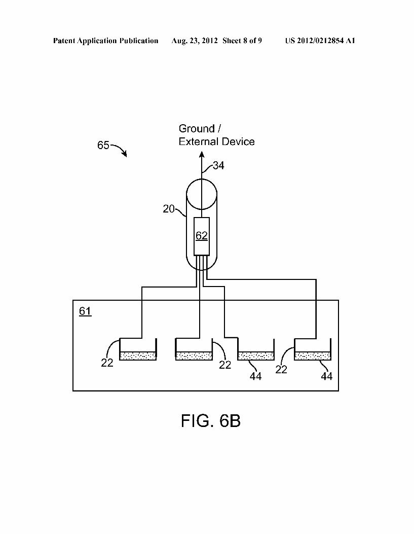
[0057] A noteworthy quantity for a T] resistor is the capaci tance (CU), as: CTJIkeOHD/L, Where k is the dielectric per meability of the insulating layer, and e0 (:8.9><l0_l2 f/m) is the dielectric permeability in a vacuum. Using a value of 1 mm2 for HD, 3 for k and 1 nm for L, yields a capacitance CH of 0.027 pf, Which is negligible for frequencies of l GHZ. The reader elements are connected to shields With the tunnel junc tion resistors. [0058] As shoWn in FIGS. 4 and 5, at least one Writer element lead is connected to a high impedance shunt, and at least one reader element lead is connected to a high imped ance shunt. In another example head assembly 60 shoWn in FIG. 6A, shunt resistors for a transducer head 61 including transducer elements 44, can be on an external chip 62 Which can be bonded to leads 22 of the transducer elements 44, and bonded to the transducer head substrate or piggyback struc ture. An example Would be to fabricate the high impedance shunt resistors on the chip 62 using either high impedance thin ?lm resistors or T] resistors or other appropriate high impedance resistors. The advantage of this approach Would be that if space on the Wafer (substrate) containing the trans ducer elements 44 is at a premium, then the chip 62 can be connected to the transducer 41 at a later stage.
[0059] Since much of the ESD damage can occur after the cable 20 containing the leads 22 is attached to the transducer elements 44, in another example head assembly 65 shoWn in FIG. 6B the chip 62 including the high impedance shunt resistors can be bonded to the ?exible cable 20 that is attached to the transducer elements 44. An advantage of attaching the shunt resistors via the chips 62 at a later stage is that defects in making the shunt resistors Would not affect the yield of the reader and Writer chips. Another advantage of attaching a shunt resistor chip 62 to the cable 20 is that if, for some reason, the processing for the shunt resistors is not available at the same facility as the reader-Writer fabrication site, then the shunt resistor chip 62 could be added elseWhere. The high impedance resistance is chosen to be high enough not to interfere With the normal operation of the readers and Writers or to couple them together. In addition, the add-on high impedance shunt resistors can be on a ?ip chip that can be attached to the cable 20 and removed doWnstream in the manufacturing process. [0060] FIG. 7 illustrates an example tape drive 70 Which may be employed in the context of the present invention. While one speci?c implementation of a tape drive is shoWn in FIG. 7, it should be noted that the embodiments of the present invention may be implemented in the context of any type of drive (i.e., hard disk drive, tape drive, etc.) The present inven tion is also useful With MR technologies With piggyback structured MR elements such as AMR, GMR and TMR tech nologies utiliZed in tape and hard disk drive manufacturing for magnetic media storage industries. [0061] As shoWn in FIG. 7, a tape supply cartridge 72 and a take-up reel 74 are provided to support a tape 76. Moreover, guides 77 guide the tape 76 across a bi-directional transducer head comprising a tape head 78. Such bi-directional tape head 78 is in turn coupled to a control assembly 80 via a MR connector cable 82 (e.g., the insulator cable 20 in FIGS. 2 and 4). A tape drive such as shoWn in FIG. 7 further includes drive motor(s) to drive the tape supply cartridge 72 and the take-up reel 74 to move the tape 76 linearly over the head 78. The tape drive also includes a read/Write channel to transmit data to the head 78 to be recorded on the tape 76 and to receive data read by the head 78 from the tape 76. An interface is also provided
Aug. 23, 2012
for communication betWeen the tape drive and a host to send and receive the data and for controlling the operation of the tape drive and communicating the status of the tape drive to the host, all as understood by those of skill in the art. [0062] The present invention has been described in consid erable detail With reference to certain preferred versions thereof; hoWever, other versions are possible. Therefore, the spirit and scope of the appended claims should not be limited to the description of the preferred versions contained herein.
What is claimed is: 1. A transducer head assembly comprising: a reader element; a Writer element; a ?rst and second impedance shunt Wherein the ?rst imped
ance shunt electrically connects to the reader element and the second impedance shunt electrically connects to the Writer element, the ?rst and second impedance shunts each connected to a common electrically conduc tive path; and
a high impedance resistive element coupled to the common electrically conductive path.
2. The transducer head assembly of claim 1, Wherein: the reader element and the Writer element are assembled as
a piggyback structure, such that the reader element is separated from the Writer elements by an electrical insu lation layer.
3. The transducer head assembly of claim 1, Wherein each of the ?rst and second impedance shunt comprises one of a thin ?lm impedance shunt resistor and a discrete impedance shunt resistor.
4. The transducer head assembly of claim 1, Wherein the common electrically conductive path maintains electrostatic charge equipotential betWeen the reader element and the Writer element When isolated from a measuring device, While providing su?icient electrical isolation during measurements and operation.
5. The transducer head assembly of claim 1, Wherein the common electrically conductive path discharges electrostatic charge from the reader element and the Writer element, Wherein each resistance device controls time dependence of discharge of accumulated electrostatic charge betWeen the reader element and the Writer element.
6. The transducer head assembly of claim 1, Wherein the transducer head comprises a bi-directional tape head coupled to a control assembly for reading data from a tape cartridge and Writing data to the tape cartridge.
7. The transducer head assembly of claim 1, Wherein the impedance shunt comprises a high impedance device dis posed on a magnetoresistive cable providing read/Write sig nals to the reader and Writer elements.
8. The transducer head assembly of claim 1, Wherein the impedance shunt comprises a high resistance device disposed on a substrate of the head assembly.
9. The transducer head assembly of claim 1, Wherein each of the ?rst and second impedance shunt comprises Tantalum ?lm deposited on a substrate of the transducer head assembly.
10. A transducer head assembly comprising: plural reader elements; plural Writer elements; plural high impedance shunts, Wherein each of the high
impedance shunts that electrically connect to the reader elements and the Writer elements to a common electrical
contact; and
US 2012/0212854 A1
a high impedance resistive element coupled to the common electrical contact.
11. The transducer head assembly of claim 10, Wherein each of the high impedance shunts provide the common elec trically conductive paths for maintaining electrostatic charge equipotential betWeen the reader elements and the Writer elements.
12. The transducer head assembly of claim 10, Wherein at least one Writer element lead is connected to a high imped ance shunt.
13. The transducer head assembly of claim 10, Wherein at least one reader element lead is connected to a high imped ance shunt.
14. The transducer head assembly of claim 10 further com prising a substrate on Which the reader and Writer elements are deposited, Wherein the high impedance shunts are depos ited on the same substrate.
15. The transducer head assembly of claim 10 further com prising a transducer substrate on Which the reader and Writer elements are deposited, Wherein the high impedance shunts are deposited on a separate substrate that is bonded to said transducer substrate.
16. The transducer head assembly of claim 10, Wherein each of the high impedance shunts is deposited on a ?ip chip Which is bonded to a cable that provides read/Write signals lines to the transducer head assembly.
17. The transducer head assembly of claim 10, Wherein the high impedance shunts comprises Tantalum ?lm resistive elements.
18. The transducer head assembly of claim 10, Wherein: the reader elements and the Writer elements are assembled
as a piggyback structure, such that each reader element is separated from a Writer element by an electrical insu lation layer.
Aug. 23, 2012
19. The transducer head assembly of claim 10, Wherein the transducer head comprises a bi-directional tape head coupled to a control assembly for reading data from a tape cartridge and Writing data to the tape cartridge.
20. The transducer head assembly of claim 19, Wherein the transducer head is integrated in a tape drive system compris ing an interface for communicating betWeen the tape drive and a host computer system.
21. A method of manufacturing a transducer head, the method comprising:
providing a transducer substrate; depositing a reader element and a Writer element on the
transducer substrate; providing an impedance substrate; depositing a ?rst impedance shunt and a second impedance
shunt on the impedance substrate; and connecting the transducer substrate and the impedance
substrate such that the ?rst impedance shunt electrically connecting the reader element and the second imped ance shunt electrically connecting the Writer element, and the ?rst impedance shunt and the second impedance shunt each connected to a common electrically conduc tive path.
22. The method of claim 21, Wherein the ?rst impedance shunt and the second impedance shunt are each deposited on a ?ip chip.
23. The method of claim 22, further comprising bonding the ?ip chip to a cable for providing read/Write signals lines to the transducer head.


![structure, Magnetic and Magnetoresistive ... - ufm.imp.kiev.ua · electronics [16]. In this case, the research of magnetoresistive and magnetic properties of composite materials based](https://static.documents.pub/doc/80x56/5eb96019b69eb6721808cf39/structure-magnetic-and-magnetoresistive-ufmimpkievua-electronics-16.jpg)


