Supplementary Information
Chemically Improved High Performance Printed Indium Gallium Zinc
Oxide Thin-Film Transistors
Sunho Jeong*a, Ji-Yoon Lee,a Sun Sook Lee,a Se-Wook Oh,b Hyun Ho Lee,b Yeong-Hui
Seo,a Beyong-Hwan Ryu,a and Youngmin Choi*a
Experimental Deatails
Precursor Solution Synthesis. All reagents, zinc acetate dihydrate (Zn(C2H3O2)2·2H2O,
98%), indium nitrate hydrate (In(NO3)3·H2O, 99.9%), and gallium nitrate hydrate
(Ga(NO3)3·H2O, 99.9%), ethylene glycol (HOCH2CH2OH, anhydrous 99.8%),
monoethanolamine (NH2CH2CH2OH, 99%), and 2-methoxyethanol (CH3OCH2CH2OH,
anhydrous 99.8%) were purchased from Aldrich and used without additional purification.
0.375 M metal precursor solutions were prepared in 2-methoxyethanol including the different
amount of ethylene glycol. The composition of ethylene glycol was varied from 0 to 30 vol%,
and chemical composition ratio of IGZO precursor solution was In:Ga:Zn = 63:10:27.
Monoethanolamine and DI-water were additionally incorporated as a stabilizer and a reactant
for hydrolysis reaction, respectively. The prepared clear solutions were stirred for 3 hr at
room temperature prior to spin coating.
Transistor Fabrication and Electrical Performance Characterization. Doped silicon
substrate with a 100 nm-thick thermal SiO2 layer, used as a gate dielectric, was sonicated
with absolute ethanol and dried with an N2 stream, followed by UV/O3 treatment for 5 min.
For fabricating the transistors with top contact device architecture, each precursor solution
was spin coated at 4000 rpm for 35 sec and 20 vol% EG added precursor solution was ink-jet
Electronic Supplementary Material (ESI) for Journal of Materials ChemistryThis journal is © The Royal Society of Chemistry 2011
printed on gate dielectric layer. The printer setup is composed of a drop-on-demand
piezoelectric inkjet nozzle manufactured by Microfab Technologies, Inc. (Plano, TX), and the
nozzle with an orifice diameter of 30 μm was used. The resulting IGZO semiconducting
layers were annealed at 400 oC for 30 min, and then Al source and drain electrodes with 50
nm thickness were deposited via thermal evaporation (pressure ~10-6 Torr) through shadow
masks. The channel length and width are 100 and 100 μm, respectively. For transistors with
bottom contact device architecture, ITO source and drain electrodes were patterned using a
photolithography and wet etching method on the top of 100 nm-thick SiO2 gate dielectric.
The channel length and width are 100 and 100 μm, respectively. 20 vol% EG added precursor
solution was ink-jet printed and then annealed at 400 oC for 30 min. In order to analyze the
contact resistance for both printed devices, a transmission line method (TLM) analysis was
carried out. For both printed TFTs with either Al or ITO electrode, the source and drain
electrodes had a fixed channel width of 100 μm and varying channel lengths between 20 and
100 μm. The electrical performance of the transistors was analyzed in ambient condition
using an Agilent E5270B source-measure unit. Saturation mobilities were extracted from the
slope of (drain current)1/2 versus gate voltage derived from the device transfer plot. All device
fabrication and measurement were carried out in ambient atmosphere.
Film Characterization. The chemical structures of oxide semiconductors were examined
by X-ray photoelectron spectroscopy (XPS, Omicron, ESCA Probe). The surface XPS data
were collected using monochromatic AlKα radiation (1486.6 eV) in an ultrahigh vacuum
system with a base pressure of ~10-10 Torr. The crystal structures were analyzed with a
grazing angle X-ray diffraction (XRD) using CuKα radiation on a Rigaku ATX-G thin-film
diffraction workstation. The grain size and surface morphology were observed by atomic
force microscope (Digital Instruments, Nano Scope IV), and the thermal behaviors of metal
Electronic Supplementary Material (ESI) for Journal of Materials ChemistryThis journal is © The Royal Society of Chemistry 2011
salt precursors were monitored using thermal gravimetric analyses (SDT2960, TA
Instruments).
Figure S1. The image showing the jetting behavior of IGZO precursor droplet ejected
through the ink-jet printing nozzle.
100 200 300 400 500
20
40
60
80
100
Wei
gh
t L
oss
(w
t%)
Temperature (oC)
Ga nitrate
In nitrate Zn acetate
Figure S2. Thermal gravimetric analysis curves of indium nitrate hydrate, zinc acetate
dihydrate, and gallium nitrate hydrate. The measurement was carried out in air.
Electronic Supplementary Material (ESI) for Journal of Materials ChemistryThis journal is © The Royal Society of Chemistry 2011
0 % 5 %
10 % 20 % 30 %
Figure S3. (a) AFM images for IGZO semiconductors prepared using precursor solution
containing the different amount of EG between 0 and 20 vol%. All IGZO layers were
annealed at 400 oC in air.
20 30 40 50
Inte
nsity
(A
.U.)
2 Theta
0 vol% 5 vol% 10 vol% 20 vol% 30 vol%
Figure S4. XRD results for IGZO semiconductors prepared using precursor solution
containing the different amount of EG between 0 and 20 vol%. All IGZO layers were
annealed at 400 oC in air.
Electronic Supplementary Material (ESI) for Journal of Materials ChemistryThis journal is © The Royal Society of Chemistry 2011
(a)
(b)
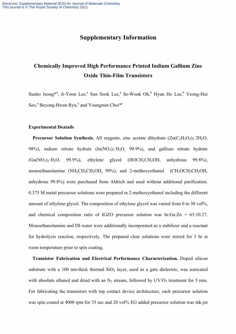
Figure S5. TEM image and selective area diffraction pattern for IGZO semiconductor layer
prepared from IGZO precursor solution containing EG of (a) 20 vol% and (b) 30 vol%.
Figure S6. AFM image for the IGZO semiconductor printed layer using a 20 % EG added
precursor solution.
Electronic Supplementary Material (ESI) for Journal of Materials ChemistryThis journal is © The Royal Society of Chemistry 2011
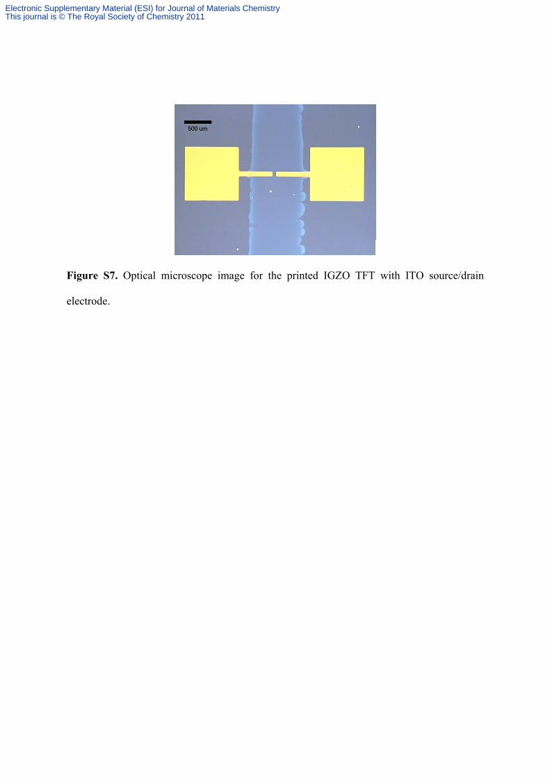
Figure S7. Optical microscope image for the printed IGZO TFT with ITO source/drain
electrode.
Electronic Supplementary Material (ESI) for Journal of Materials ChemistryThis journal is © The Royal Society of Chemistry 2011


![Bis[tris(1,10-phenanthroline)nickel(II)] tris ... · Bis[tris(1,10-phenanthroline)nickel(II)] tris[dicyanidoargentate(I)] nitrate 4.2-hydrate Muhammad Monim-ul-Mehboob,a Muhammad](https://static.documents.pub/doc/80x56/5f74462041fcef38863090d7/bistris110-phenanthrolinenickelii-tris-bistris110-phenanthrolinenickelii.jpg)


