EVALUATION BOARD FOR THE Si2401 WITH A UART INTERFACE
Description
The Si2401FS10-EVB evaluation board provides thesystem designer an easy way of evaluating the Si2401ISOmodem®. The Si2401FS10-EVB consists of amotherboard with a power supply, an RS-232 and USBinterface, other ease-of-use features, and a completeremovable modem module on a daughter card. (Afunctional block diagram of the Si2401FS10-EVB isshown below.) The Si2401 ISOmodem is a completecontroller-based modem chipset integrating SiliconLabs’ third-generation, globally-programmable directaccess arrangement (DAA). Available as two 16-pinsmall outline (SOIC) packages, the Si2401 ISOmodemeliminates the need for a separate DSP data pump,modem controller, memories, codec, isolationtransformer, relays, opto-isolators, and a 2- to 4-wirehybrid. The Si2401 is ideal for embedded modemapplications due to its small board area, controller-based architecture, low power consumption, and globalcompliance. The Si2401FS10-EVB provides an RJ-11jack for interfacing to the phone line and a DB9 or USBconnector for interfacing the Si2401FS10-EVB to a PCor data terminal serial port. This allows the Si2401ISOmodem to operate as a serial modem forstraightforward evaluation. To evaluate the Si2401ISOmodem in an embedded system, the daughter cardcan be used independently or with the motherboard.
A direct access header (JP3) is available on themotherboard to bypass the RS-232 transceivers andconnect the Si2401 ISOmodem directly to a targetsystem.
Power is supplied through a screw terminal (J3) or astandard 2 mm power jack (J4). An onboard rectifier,filter, and voltage regulator allow the power input to be7.5–13 V ac or dc (either polarity). Alternatively, powercan be supplied through the USB interface (whether theUSB or an RS232 interface is used). The Si2401FS10-EVB can drive an external speaker for call monitoring,or a piezoelectric speaker can be mounted directly onthe board in the space provided.
Features
The Si2401FS10-EVB includes the following:
Dual RJ-11 connection to phone line RS-232 and USB interface to PC Audio connector for call monitoring Direct access to Si2401 for embedded application
evaluation Easy power connection to common 7.5–13.5 V
power supplies or USB port 9 V ac adaptor Simple installation and operation
Functional Block Diagram
Rectifier Filter
7.5–13.5 V dc orpeak ac
RS-232Transceivers
UARTDB9
InterfaceSelectionJumpers
Si2401
Push ButtonReset
RESET XTALIXTALO
Si3010InterfaceCircuit
RJ-11
PhoneLine
AudioAmplifier
AOUT
AudioOut
DirectAccess HDR
Daughter Board Boundary
VoltageRegulator 3.3 V
5 V
Power-OnReset
9 V dc at 300 mA acAdaptor
USBConnector
USB I/F
Si2401FS10-EVB
2 Rev. 1.1
1. Introduction
Notable differences between the Si2401 and otherISOmodem products are highlighted in the bulleted listbelow. For complete details and specifications, refer tothe current Si2401 data sheet.
Unique Si2401 Features:
Many AT commands execute when entered without <CR>.
S-Register address and value are entered in hex (example: ATS0F = 2B).
Result codes are abbreviated (example: “O” instead of “OK”).
The Si2401DC power must be 3.3 V.
Several AT commands are required to enable the speaker:ATSE2 = 80 configures GPIO4 for AOUT.ATSF4 = 00 removes Tx and Rx audio mute.ATM2 turns on speaker continuously.
DTE interface default is 8N1, 2400 bps, hardware flow control, and no linefeeds with carriage returns.
ATDT is disabled if linefeeds with carriage returns are enabled.
Some common AT Commands are not available:A/ATD (must be ATDT or ATDP)AT&Tn (use ATSE4=20 for local digital loopback)
2. Si2401FS10-EVB Setup and Evaluation
This section explains how to set up the Si2401FS10-EVB for evaluation as an RS-232 or USB interfacemodem. Jumper settings, power connection, PC/terminal connections, and terminal programconfiguration settings are given. After power is applied,the initial modem setup and a basic tutorial on modemoperation are provided. The Si2401FS10-EVBconfigurations for evaluating additional features arediscussed separately.
2.1. Si2401FS10-EVB Quick Start—RS-232Interface
1. Set jumpers according to Figure 1.
2. Connect:
DB-9 to PC COM 1 (with a pass-through cable).RJ-11 to phone line or test box.the 9 V ac adaptor (or USB cable).
3. Bring up:
Turn on power to modem.Set Terminal Program for 2400 bps 8N1. Hardware flow control. Disable linefeeds with carriage returns (linefeeds with carriage returns disable ATDT commands.)
4. Type “AT” followed by a carriage return.
Should echo “AT” and then an “O”.5. Type:
ATS00 = 01 for auto-answer on first ring.
2.2. Si2401 FS10-EVB Quick Start—USB Interface
1. Set jumpers according to Figure 2.
2. Connect:
USB cable to PC.RJ-11 to phone line or test box.
3. Download USB driver for your operating system from the CD supplied with the evaluation board.
4. Install driver.
5. Bring up:
Reset the modem.Set Terminal Program for 2400 bps 8N1. Hardware flow control. Disable linefeeds with carriage returns (linefeeds with carriage returns disable ATDT commands).
6. Type “AT” followed by a carriage return.
Should echo “AT” and then an “O”.7. Type:
ATS00=01 for auto-answer on first ring.
Table 1. Modem Configuration Examples
Modulation ATS07 =
V22bis 06
V.22 02
V.21 03
Bell 212A 00
Bell 103 01
V.23 (1200 TX, 75 RX—Answer) 14
V.23 (75 TX, 1200 RX—Originate) 24
V.23 (600 TX, 75 RX—Answer) 10
V.23 (75 TX, 600 RX—Originate) 20
Table 2. Modem Initialization Example
Command Function
ATS00 = 02 Auto-answer after two rings
ATS07 = 06 Configures modem for V.22b
ATSF4 = 00 Removes audio mute
ATM1 Turns on speaker until carrier negotiated
Si2401FS10-EVB
Rev. 1.1 3
2.3. Jumper SettingsCheck all jumper settings on the Si2401FS10-EVB before applying power. Figure 1 shows the standard factoryjumper settings. These settings configure the Si2401FS10-EVB for RS-232 serial operation. Any standard terminalprogram configured to communicate through a PC COM port can be used to communicate with the Si2401FS10-EVB. To connect the modem directly into an embedded system with LVCMOS/TTL levels, install JP8 to disableboth the RS-232 and USB interfaces. Connection to the embedded system can be made to JP-3. Place a jumperon JP13 to enable the onboard speaker, LS1.
Figure 1. Standard Factory Jumper Settings—RS-232 Interface (Outlined in Gray)
Figure 2. Standard Factory Jumper Settings—USB Interface (Outlined in Gray)
Si2401FS10-EVB
4 Rev. 1.1
2.4. Power RequirementsThe Si2401FS10-EVB has an onboard diode bridge,filter capacitor, and voltage regulator. Power can besupplied from any source capable of providing 7.5–13 Vdc or 7.5–13 V peak ac and at least 100 mA. (Additionalcurrent may be required if a speaker is connected formonitoring call progress tones.) Power may be appliedto the Si2401FS10-EVB through the screw terminals(J3) or the 2 mm power jack (J4). The onboard full-waverectifier and filter ensure that the correct polarity isapplied to the Si2401FS10-EVB. Daughter card poweris supplied through voltage regulator U2 and is factory-set at 3.3 V. Power is also supplied by the USB cableand can be used regardless of whether the modem isconfigured for the USB, RS-232, or direct interfacemode. Daughter card current can be measured byconnecting an ammeter between JP7 pins 1 and 2.These pins must always be connected. Failure toconnect pins 1 and 2 of JP7 through either a jumper or alow-impedance ammeter may result in damage to theSi2401FS10-EVB.
2.5. Terminal and Line ConnectionsThe Si2401 can be tested as a standard serial datamodem by connecting the Si2401FS10-EVB to apersonal computer or other data terminal equipment(DTE), phone line, and power. Connect a PC, RS-232,or USB interface to the Si2401FS10-EVB with theappropriate cable. The RS-232 transceivers on the EVBcan communicate with the DTE at rates of up to 1 Mbps.Any standard terminal program, such as HyperTerminalor ProComm, running on a PC can communicate withthe Si2401FS10-EVB. Configure the terminal emulationprogram to 2400 bps, 8 data bits, no parity, one stop bit,and hardware flow control. Also, be sure to disablelinefeeds with carriage returns. Connect the RJ-11 jackon the Si2401FS10-EVB to an analog phone line ortelephone line simulator, such as a Teltone TLS 5.
2.6. Making ConnectionsWith the terminal program properly configured andrunning, apply power to the Si2401FS10-EVB. Type“AT<CR>”, and the modem should return “O” indicatingthe modem is working in the command mode andcommunicating with the terminal. If the “O” response isnot received, try resetting the modem by pressing themanual reset switch (S1); then type “AT<CR>” again.
To take the modem off-hook, type “ATDT<CR>.” Themodem should go to the off-hook state, draw loopcurrent, and respond with a “t”, indicating a dial tonedetection. Typing any characters makes the modemhang up (go on-hook) and stop drawing loop current.
To make a modem connection, type “ATDT(calledmodem phone number)<CR>.” Once the connection isestablished, a “c” message appears, indicating the twomodems are in the data mode and communicating.Typing on one terminal should appear on the otherterminal. To return to the command mode withoutinterrupting the connection between the two modems,type “+++.” Approximately two seconds later, “O” willappear. The modem is now in command mode and willaccept “AT” commands. To return to data mode, type“ATO.” The modem resumes the data connection andno longer accepts AT commands. Type “ATH” toterminate the data connection.
3. Si2401FS10-EVB Functional Description
The Si2401FS10-EVB is a multipurpose evaluationsystem. The modem daughter card illustrates the smallsize and small number of components required toimplement an entire controller-based modem withglobal telecommunications compatibility. The daughtercard can be used independently of, or in conjunctionwith, the motherboard. The motherboard adds featuresthat enhance the ease of evaluating the manycapabilities of the Si2401 ISOmodem®.
3.1. MotherboardThe motherboard provides a convenient interface to theSi2401DC (daughter card). The versatile power supplyallows for a wide range of ac and dc voltages to powerthe board. RS-232 transceivers and a DB9 connectorallow the Si2401FS10-EVB to be easily connected to aPC or other terminal device. Jumper options allow directaccess to the LVCMOS/TTL level serial inputs to theSi2401, bypassing the RS-232 transceivers or USBinterface. This is particularly useful for directlyconnecting the Si2401 to embedded systems.
The Si24xxFS10-EVB motherboard connects to thedaughter card through two connectors, JP1 and JP2.JP1 is an 8x2 socket providing connection to all Si2401digital signals and regulated 3.3 V power for the Si2401.The Si2401 digital signals appearing at JP1 (daughtercard interface) are LVCMOS- and TTL-compatible. TheSi2401DC must be powered by 3.3 V. The motherboardis factory-configured for 3.3 V with JP7 pins 1 and 2.JP2 is a 4x1 socket providing connection between thedaughter card and the RJ-11 phone jack.
Si2401FS10-EVB
Rev. 1.1 5
3.1.1. Voltage Regulator/Power Supply
The input voltage to either J3 or J4 must be between 7.5and 13.5 V dc or 7.5 and 13.5 VPEAK ac. Themotherboard includes a diode bridge (D1–D4) to guardagainst a polarity reversal of the dc voltage or to rectifyan ac voltage. The power source must be capable ofcontinuously supplying at least 100 mA. C50 serves asa filter cap for an ac input. The voltage regulator, U1,provides 5 V for the motherboard and the input forvoltage regulator U2, which outputs 3.3 V for use on themotherboard and to power the daughter card. Si24xxDCpower consumption can be measured by placing ameter between pins 1 and 2 of JP7. The connectionbetween JP7 pins 1 and 2 must be made at all timeswhen power is applied to the evaluation board eitherthrough a jumper block or a low-impedance meter toavoid damage to the daughter card. Power is suppliedto U2 through D5 from the USB.
3.1.2. Reset Circuitry
The Si2401 requires a reset pulse to remain low for atleast 5.0 ms after the power supply has stabilized duringthe powerup sequence or for at least 5.0 ms during apower-on reset, then go high with a rise time <100 ns.Most production Si2401 modem chipset applicationsrequire that RESET be controlled by the host processor.Certain Si2401 operation modes, including Powerdown,require a hardware reset to recover.
The Si2401FS10-EVB contains two reset options, anautomatic power-on reset device, U3 (DS1818)(default), and a manual reset switch (S1) to permitresetting of the chip without removing power.Regardless of the mechanism, a reset causes allmodem settings to revert to factory default values. SeeFigure 6 on page 11 and Figure 8 on page 13 for thereset circuit schematic.
3.1.3. DS1818
The DS1818 is a small, low-cost device that monitorsthe voltage on VD and an external reset pushbutton. IfVD drops below 3.0 V, the DS1818 provides a 220 msactive-low reset pulse. On power-up, the DS1818 alsooutputs an active low reset pulse for 220 ms after VDreaches 90% of the nominal 3.3 V value. The DS1818outputs a 220 ms reset pulse any time the power supplyvoltage exceeds the 3.3 V ±10% window.
3.1.4. Manual Reset
The manual reset switch (S1) performs a power-onreset. This resets the Si2401 to factory defaults withoutturning off power. If S1 is used in conjunction with U6,pressing S1 activates the reset monitor in the DS1818and produces a 220 ms active low reset pulse.
3.1.5. Interface Selection
The serial interface of the Si2401FS10-EVB can beconnected to a computer terminal, embedded system,or any other Data Terminal Equipment (DTE) via astandard RS-232 interface, USB interface, or direct TTLserial interface.
The Si2401 can be tested as a standard data modem byconnecting the Si2401FS10-EVB to a personalcomputer or other DTE, power supply, and a phone line.A PC can communicate with the Si2401FS10-EVBusing a standard terminal program, such as HyperTermor ProComm.
Jumper settings determine how the Si2401FS10-EVB isconnected to the DTE. Table 3 lists the interfacecontrolled by each motherboard jumper. See Figure 7on page 12 and Figure 17 on page 22.
3.1.6. RS-232 Interface
This operation mode uses the standard factory jumpersettings illustrated in Figure 1 on page 3. The MaximMAX3237 transceiver interfaces directly with the TTLlevels available at the serial interface of the Si2401 and,using internal charge pumps, makes these signalscompatible with the RS-232 standard. The RS-232transceiver on the Si2401FS10-EVB can communicateat rates between 300 bps and 1 Mbps. This simplifiesthe connection to PCs and other Data TerminalEquipment (DTE). The signals available on theSi2401FS10-EVB serial interface (DB9 connector) arelisted in Table 4.
Table 3. Interface Selection Jumpers
Jumper Function
JP1 Daughter Card Phone Line Connector.
JP2 Daughter Card Digital Connector.
JP3 Direct Access Header.
JP4 Not Used.
JP5 USB Enable (RS-232 Disable).
JP6 Options.
JP7 3.3 V Power for Daughter Card.
JP8 Disable both RS-232 and USB.
JP9 Not Used.
JP10 Not Used.
JP11 Not Used.
JP12 Enable 27 MHz Clock Option.
Si2401FS10-EVB
6 Rev. 1.1
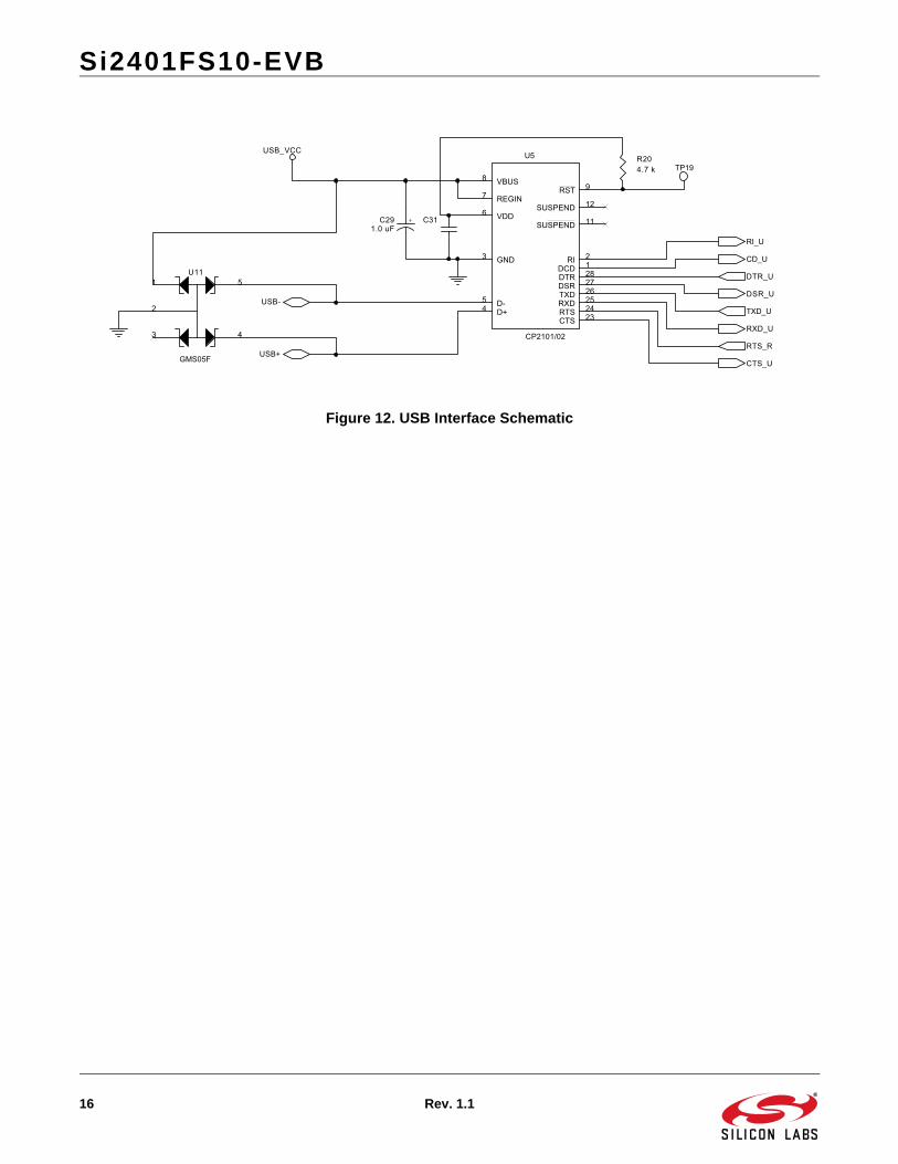
3.1.7. USB InterfaceThe USB cable connects to J5 on the motherboard andprovides both data and power. Installing a jumper onJP5 enables the USB interface and disables the RS-232interface. The USB interface is provided by U5. A USBdriver for this chip is available for most PC and MACoperating systems on the CD.
3.1.8. Direct Access Interface
The motherboard supplies power through J3, J4, orUSB, power-on reset, and an RJ-11 jack for the modem.The direct access interface (JP3) is used to connect themotherboard to an embedded system. JP3 providesaccess to all Si2401 signals available on the daughtercard. It is necessary to install a jumper on JP8 to disableboth the RS-232 and USB interface and prevent signalcontention. Leave the jumper between JP7 pins 1 and2. Figure 3 illustrates the jumper settings required forthe direct access mode using the motherboard.
Figure 3. Jumper Settings for Direct Access Interface
Table 4. DB9 Pin Connections
J1 Name J1 Symbol J1 Pin Si2401 Pin Si2401 Name
Carrier Detect CD 11
Received Data RXD 2 5 RXD
Transmit Data TXD 3 6 TXD
Data Terminal Ready DTR 42 14 ESC/GPIO3
Signal Ground SG 5 12 GND
Data Set Ready DSR 6 Note 3
Ready to Send RTS 7 nc
Clear to Send CTS 8 7 CTS
Ring Indicator RD 91 nc
Notes:1. JP6 + JP5 jumper option.2. JP6 Jumper option.3. DSR connected to DTR at J1.
Si2401FS10-EVB
Rev. 1.1 7
3.1.9. Audio Output
Audio output is provided from the Si2401 on the pin,AOUT. This signal allows the user to monitor callprogress signals, such as dial tone, DTMF dialing, ring,busy signals, and modem negotiation. Control of thissignal is provided by AT commands and registersettings described in the introduction. The AOUT signalcan be connected to an amplifier, such as the LM386(the default stuffing option on the Si2401FS10-EVB), forhigh-quality output. AOUT can also be connected to asumming amplifier or multiplexer in an embeddedapplication as part of an integrated audio system.
3.1.10. Amplifier (LM386)
The audio amplifier circuit consists of U10 (LM386),C20, R3, R4, C21, C22, C23, R5, C24, and an optionalloudspeaker, LS1. The LM386 has an internally-setvoltage gain of 20. R3 and R4 provide a voltage dividerto reduce the AOUT signal to prevent overdriving theLM386. C20 provides dc blocking for the input signaland forms a high-pass filter with R3+R4, while R4 andC21 form a low-pass filter. These four components limitthe bandwidth of the AOUT signal. C22 provides high-frequency power supply bypassing for the LM386 andshould be connected to a hard ground and located veryclose to the amplifier’s power supply and ground pins.C23 and R5 form a compensation circuit to preventoscillation of the high-current PNP transistor in theLM386 output stage on negative signal peaks. Theseoscillations can occur between 2–5 MHz and can posea radiation compliance problem if C23 and R5 areomitted. C24 provides dc blocking for the output of theLM386, which is biased at approximately 2.5 V (VCC/2),and forms a high-pass filter with the impedance of theloudspeaker (LS1). The output from the LM386 amplifiercircuit is available on the RCA jack, J2 (not installed).Install jumper JP13 to enable the onboard speaker,LS1.
3.2. Modem Module OperationThe Si2401FS10-EVB daughter card is a completemodem solution perfectly suited for use in an embeddedsystem. The daughter card requires a 3.3 V supplycapable of providing at least 35 mA and communicates
with the system via LVCMOS/TTL-compatible digitalsignals on JP1. The RJ-11 jack (TIP and RING) isconnected via JP2. Be sure to provide the properpower-on reset pulse to the daughter card if it is used inthe standalone mode.
3.2.1. Reset Requirements
The Si2401 ISOmodem daughter card must be properlyreset at powerup. The reset pin (pin 8) of the Si2401,(JP1, pin 13), must be held low for at least 5.0 ms afterpower is applied and stabilized and returned high with arise time less than 100 ns to ensure that the device isproperly reset.
3.2.2. Crystal Requirements
Clock accuracy and stability are important in modemapplications. To ensure reliable communicationbetween modems, the clock must remain within±100 ppm of the design value over the life of themodem. The crystal selected for use in a modemapplication must have a frequency tolerance of lessthan ±100 ppm for the combination of initial frequencytolerance, drift over the normal operating temperaturerange, and five-year ageing. Other considerations, suchas production variations in PC board capacitance andthe tolerance of loading capacitors, must also be takeninto account.
3.2.3. Protection
The Si2401FS10-EVB meets or exceeds all FCC andinternational PTT requirements and recommendationsfor high-voltage surge and isolation testing without anymodification. The protection/isolation circuitry includesC1, C2, C8, C9, FB1, FB2, and RV1. The PCB layout isalso a key “component” in the protection circuitry. TheSi2401FS10-EVB provides isolation to 3 kV. ContactSilicon Laboratories for information about designing tohigher levels of isolation.
4. Design
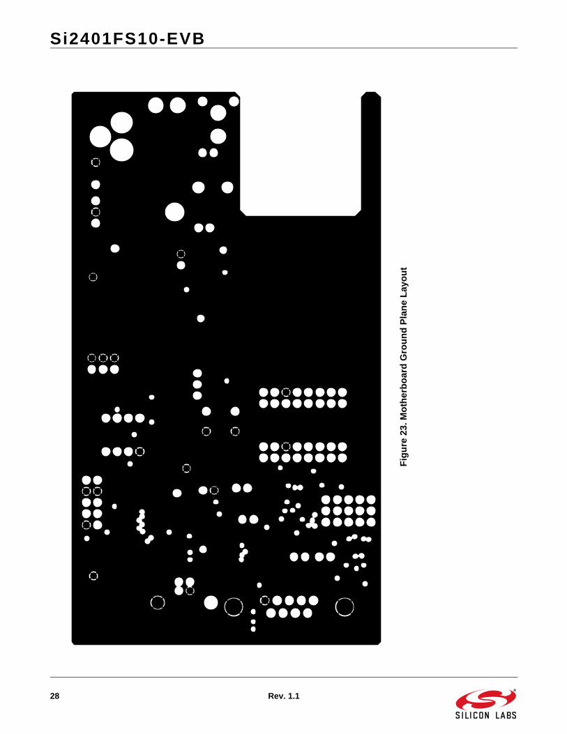
The following pages contain the schematics, bill ofmaterials, and layout for the Si2401 including thedaughter card and motherboard.
Si2401FS10-EVB
8 Rev. 1.1
RX
CLK
DC
Db
ES
CA
OU
T
RX
D
RE
SE
Tb
XT
ALI
XTA
LO XT
ALI
XTA
LO
RX
DR
TS
b
RE
SE
Tb
DC
Db
RX
D
TX
CLK
RT
Sb
INT
b
ES
C
RIb
EE
SD
AO
UT
CL
KO
UT
CL
KO
UT
TXD
TXD
CT
Sb
CT
Sb
TXD
CT
Sb
VD
AVD
A
TX
CLK
RX
CLK
RX
CLK
EE
SD
RIb
AO
UT
TX
CLK
INT
b
ES
C
RE
SE
Tb
DC
Db
DC
Db
INT
b
RIb
AO
UT
EE
SD
VD
D
VD
D
VD
D
C1
A
C2
A C1
A
C2
A
TIP
RIN
G
C1
A
C2
A
Over
lap
the 16-pin SOIC and 24-pin TSSOP
TXD
GPIO
5/RIb/TXCLK
- RXD
CTSb
Si2401
GPIO3/ESC
- GPIO2/DCDb
RESETb
-GPIO
1/EOFR/RXCLK
-
"Si2
4xx2
G-DC
Rev
. 1.
0 IS
Omod
em T
M"
-
Thes
e components
for internal
Sila
bs use only.
GPIO
4/INTb/AOUT
JP1 Function
Pin
1 3 5 7 9 11 13 2 4 8 10 12 14 16
Thes
e components
for internal
Sila
bs use only.
R2
0
R2
3
C4
1
R1
8
1.3
k
C5
2
C5
1
R1
90
JP2
C4
0
U3
CLK
IN/X
TA
LI1
XT
ALO
2
CLK
OU
T/A
0/E
EC
S3
alt_
RI/D
6/T
XC
LK4
VD3.35
GND6
VDA7
RT
S/D
78
VDB19
GND20
VD 3.321
C2A
13
C1A
14
ES
C/D
322
DC
D/D
423
EE
CLK
/D5/
RX
CLK
24
CT
S/C
S/A
LE11
RX
D/R
D9
TX
D/W
R10
RE
SE
T12
RI/D
117
EE
IO/D
218
AO
UT
/INT
15
INT
/D0
16
C5
0
C5
5
Y1
1 2
R2
1
C5
3
U1
Si2
401
CLK
IN/X
TA
LI1
XT
ALO
2
GP
IO5/
RI/T
XC
LK3
VD3.34
RX
D5
TX
D6
CT
S7
RE
SE
T8
C2A
9
C1A
10
GP
IO4/
INT
/AO
UT
11
GND12
VA13
GP
IO3/
ES
C14
GP
IO2/
CD
15G
PIO
1/E
OF
R/R
XC
LK16
+C
54
R2
2
JP1 H
EA
DE
R 8
X2
1 3 5 7 9 11 13 15
2 4 6 8 10 12 14 16
C5
6
FB
5
Fig
ure
4.
Si2
401
Sc
he
ma
tic
Si2401FS10-EVB
Rev. 1.1 9
C1A
C2A
RIN
G
TIP
R30,
R31
, R3
2, R
33,
C30
and
C31
are
an o
ptio
nal
CID
popu
lati
on
No
Gro
und
Pla
ne In
DA
A S
ectio
n
Bias
Ring
Det
ect/
CID
Hook
swit
chDC
Ter
m
R4
Q2
Q3
R13
R16
R11
R32
C31
C9
C7
R5
R1
R30
C10
R2
R10
Q4
R12
FB2
C5
R8
+
C4
RV
1Q
5
C2
U2
Si3
010
QE
1
DC
T2
RX
3
IB4
C1B
5
C2B
6
VR
EG
7
RN
G1
8
DC
T216
IGND 15
DC
T314
QB
13
QE
212
SC 11
VR
EG
210
RN
G2
9
C6
C30
-+
D1
Z1
C1
C8
Q1
R3
R15
C3
FB1
R6
R7
R33
R31
R9
Fig
ure
5.S
i30
10 D
AA
Sc
hem
atic
Si2401FS10-EVB
10 Rev. 1.1
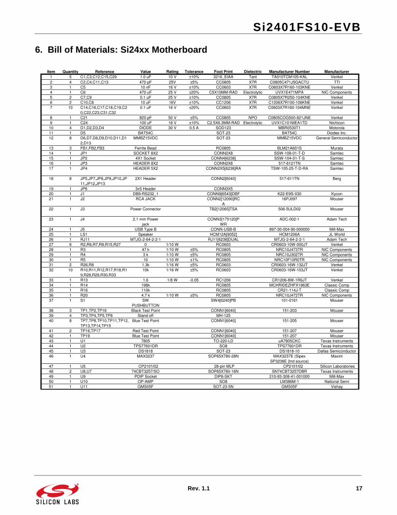
5. Bill of Materials: Si2401 Daughter Card
Value Rating Tolerance Foot Print Dielectric Manufacturer Number Manufacturer1 2 C2,C1 33 pF Y2 ±20% 1808 X7R GA342D1XGF330JY02L Murata2 1 C3 10 nF 250 V ±20% 0805 X7R C0805X7R251-103MNE Venkel3 1 C4 1.0 uF 50 V ±20% Size A Al
ElectrolyticNACE1R0M50V NIC Components
4 3 C5,C6,C50 0.1 uF 16 V ±20% 0603 X7R C0603X7R160-104MNE Venkel5 1 C7 2.7 nF 50 V ±20% 0603 X7R C0603X7R500-272MNE Venkel6 2 C9,C8 680 pF Y3 ±10% 1808 X7R GA342QR7GD681KW01L Murata7 1 C10 0.01 uF 16 V ±20% 0603 X7R C0603X7R160-103MNE Venkel8 2 C41,C40 33 pF 16 V ±5% 0603 NPO C0603NPO160-330JNE Venkel9 1 C51 0.22 uF 16 V ±20% 0603 X7R C0603X7R160-104MNE Venkel10 1 C54 1.0 uF 10 V ±10% Case A Tant TA010TCM105-KAL Venkel11 1 D1 HD04 400 V Mini-DIP HD04-T Diodes, Inc.12 2 FB2,FB1 Ferrite Bead 0603 BLM18AG601S MuRata13 1 FB5 Ferrite Bead 0603 BLM18AG601S Murata14 1 JP1 HEADER 8X2 2x8 Surface Mount
Header, .1 spaceTSM-108-01-T-DV Samtec
15 1 JP2 4X1 Header_0 CONN1X4-100-SMT
68000-403 Berg
16 2 Q3,Q1 NPN 300 V SOT-23 MMBTA42LT1 On Semi17 1 Q2 PNP 300 V SOT-23 MMBTA92LT1 On Semi18 2 Q4,Q5 NPN 80 V SOT-23 MMBTA06LT1 On Semi19 1 RV1 SiDactor 275 V 100 A SOD 6 P3100SB Teccor20 1 R1 1.07 K 1/2 W ±1% 1210 CR1210-2W-1071FT Venkel21 1 R2 150 1/16 W ±5% 0402 CR0402-16W-150JT Venkel22 1 R3 3.65 K 1/2 W ±1% 1210 CR1210-2W-3651FT Venkel23 1 R4 2.49 K 1/2 W ±1% 1210 CR1210-2W-2491FT Venkel24 2 R5,R6 100 K 1/16 W ±5% 0402 CR0402-16W-104JT Venkel25 2 R8,R7 20 M 1/8 W ±5% 0805 CR0805-8W-206JT Venkel26 1 R9 1 M 1/16 W ±1% 0402 CR0402-16W-1004FT Venkel27 1 R10 536 1/4 W ±1% 1206 CR1206-4W-5360FT Venkel28 1 R11 73.2 1/2 W ±1% 1210 CR1210-2W-73R2FT Venkel29 4 R12,R13,R15,R16 0 1/16 W ±1% 0603 CR0603-16W-000F Venkel30 1 U1 Si2401 16pin SOIC Si2401-KS Silicon Laboratories31 1 U2 Si3010 16pin SOIC Si3010-KS Silicon Laboratories32 1 Y1 4.9152Mhz 20pF load,
7. Complete Design Package (see sales representative for details)
Silicon Laboratories can provide a complete design package of the Si2401FS10-EVB including the following:
OrCad Schematics
Gerber Files
BOM
Documentation
Please contact your local sales representative or Silicon Laboratories headquarter sales for ordering information.
Si2401FS10-EVB
Rev. 1.1 31
DOCUMENT CHANGE LIST
Revision 0.6 to Revision 0.7 Changed from Rev 1.0 to Rev 3.1 Motherboard.
Revision 0.7 to Revision 0.8 Changed from Rev.1.0 to Rev.1.1 Daughter Card.
Revision 0.8 to Revision 0.9 Changed from Rev.3.1 to Rev.3.2 Motherboard.
Revision 0.9 to Revision 1.0 Changed from Rev.1.1 to Rev.1.2 Daughter Card.
Revision 1.0 to Revision 1.1 Updated "Introduction‚" on page 2.
Updated "Si2401FS10-EVB Quick Start—RS-232 Interface‚" on page 2.
Updated "Si2401 FS10-EVB Quick Start—USB Interface‚" on page 2.
DisclaimerSilicon Laboratories intends to provide customers with the latest, accurate, and in-depth documentation of all peripherals and modules available for system and software implementers using or intending to use the Silicon Laboratories products. Characterization data, available modules and peripherals, memory sizes and memory addresses refer to each specific device, and "Typical" parameters provided can and do vary in different applications. Application examples described herein are for illustrative purposes only. Silicon Laboratories reserves the right to make changes without further notice and limitation to product information, specifications, and descriptions herein, and does not give warranties as to the accuracy or completeness of the included information. Silicon Laboratories shall have no liability for the consequences of use of the information supplied herein. This document does not imply or express copyright licenses granted hereunder to design or fabricate any integrated circuits. The products must not be used within any Life Support System without the specific written consent of Silicon Laboratories. A "Life Support System" is any product or system intended to support or sustain life and/or health, which, if it fails, can be reasonably expected to result in significant personal injury or death. Silicon Laboratories products are generally not intended for military applications. Silicon Laboratories products shall under no circumstances be used in weapons of mass destruction including (but not limited to) nuclear, biological or chemical weapons, or missiles capable of delivering such weapons.
Trademark InformationSilicon Laboratories Inc., Silicon Laboratories, Silicon Labs, SiLabs and the Silicon Labs logo, CMEMS®, EFM, EFM32, EFR, Energy Micro, Energy Micro logo and combinations thereof, "the world’s most energy friendly microcontrollers", Ember®, EZLink®, EZMac®, EZRadio®, EZRadioPRO®, DSPLL®, ISOmodem ®, Precision32®, ProSLIC®, SiPHY®, USBXpress® and others are trademarks or registered trademarks of Silicon Laboratories Inc. ARM, CORTEX, Cortex-M3 and THUMB are trademarks or registered trademarks of ARM Holdings. Keil is a registered trademark of ARM Limited. All other products or brand names mentioned herein are trademarks of their respective holders.
http://www.silabs.com
Silicon Laboratories Inc.400 West Cesar ChavezAustin, TX 78701USA