55
SiFive E51 Core Complex Series Manual v1p2 c SiFive, Inc.

SiFive E51 Core Complex Series Manualv1p2
c© SiFive, Inc.

2 SiFive E51 Core Complex Series Manual v1p2
SiFive E51 Core Complex SeriesManual
Proprietary NoticeCopyright c© 2016-2017, SiFive Inc. All rights reserved.
Information in this document is provided “as is”, with all faults.
SiFive expressly disclaims all warranties, representations and conditions of any kind, whether ex-press or implied, including, but not limited to, the implied warranties or conditions of merchantabil-ity, fitness for a particular purpose and non-infringement.
SiFive does not assume any liability rising out of the application or use of any product or circuit, andspecifically disclaims any and all liability, including without limitation indirect, incidental, special,exemplary, or consequential damages.
SiFive reserves the right to make changes without further notice to any products herein.
Release Information
Version Date Changesv1p2 October 11th, 2017
• Core Complex branding• Added references• Updated interrupt chapter
v1p1 August 25th, 2017
• Updated text descriptions• Updated register and memory map tables for
consistency
v1p0 May 4th, 2017 Initial release
• Describes the functionality of the SiFive E51Core Complex
i

ii SiFive E51 Core Complex Series Manual v1p2
Contents
SiFive E51 Core Complex Series Manual i
1 Introduction 1
1.1 SiFive E51 Core Complex Overview . . . . . . . . . . . . . . . . . . . . . . . . . . 1
1.2 RISC-V Core . . . . . . . . . . . . . . . . . . . . . . . . . . . . . . . . . . . . . . . 3
1.3 Memory System . . . . . . . . . . . . . . . . . . . . . . . . . . . . . . . . . . . . . 3
1.4 Interrupts . . . . . . . . . . . . . . . . . . . . . . . . . . . . . . . . . . . . . . . . . 3
1.5 Debug Support . . . . . . . . . . . . . . . . . . . . . . . . . . . . . . . . . . . . . 3
1.6 External TileLink Interfaces . . . . . . . . . . . . . . . . . . . . . . . . . . . . . . . 3
2 Terminology 5
3 E51 RISC-V Core 7
3.1 Instruction Memory System . . . . . . . . . . . . . . . . . . . . . . . . . . . . . . 7
3.1.1 I-Cache Reconfigurability . . . . . . . . . . . . . . . . . . . . . . . . . . 8
3.2 Instruction Fetch Unit . . . . . . . . . . . . . . . . . . . . . . . . . . . . . . . . . . 8
3.3 Execution Pipeline . . . . . . . . . . . . . . . . . . . . . . . . . . . . . . . . . . . . 8
3.4 Data Memory System . . . . . . . . . . . . . . . . . . . . . . . . . . . . . . . . . . 9
3.5 Atomic Memory Operations . . . . . . . . . . . . . . . . . . . . . . . . . . . . . . 9
3.6 Local Interrupts . . . . . . . . . . . . . . . . . . . . . . . . . . . . . . . . . . . . . 9
3.7 Supported Modes . . . . . . . . . . . . . . . . . . . . . . . . . . . . . . . . . . . . 9
3.8 Physical Memory Protection (PMP) . . . . . . . . . . . . . . . . . . . . . . . . . . 9
3.9 Hardware Performance Monitor . . . . . . . . . . . . . . . . . . . . . . . . . . . . 10
4 E51 Core Complex Interfaces 13
4.1 Clock & Reset . . . . . . . . . . . . . . . . . . . . . . . . . . . . . . . . . . . . . . 13
4.1.1 Real Time Clock (rtc toggle) . . . . . . . . . . . . . . . . . . . . . . . . 13
iii
iv SiFive E51 Core Complex Series Manual v1p2
4.1.2 Peripheral Clock (clock) . . . . . . . . . . . . . . . . . . . . . . . . . . . 14
4.2 Ports . . . . . . . . . . . . . . . . . . . . . . . . . . . . . . . . . . . . . . . . . . . 14
4.2.1 TileLink Platform Ports . . . . . . . . . . . . . . . . . . . . . . . . . . . . 14
4.2.2 TileLink Front Port . . . . . . . . . . . . . . . . . . . . . . . . . . . . . . 14
4.3 Local Interrupts . . . . . . . . . . . . . . . . . . . . . . . . . . . . . . . . . . . . . 15
4.4 Global Interrupts . . . . . . . . . . . . . . . . . . . . . . . . . . . . . . . . . . . . . 15
4.5 DTIM Sizing . . . . . . . . . . . . . . . . . . . . . . . . . . . . . . . . . . . . . . . 15
4.6 Debug Output Signals . . . . . . . . . . . . . . . . . . . . . . . . . . . . . . . . . . 15
4.7 JTAG Debug Interface Pinout . . . . . . . . . . . . . . . . . . . . . . . . . . . . . . 16
5 Memory Map 17
6 Interrupts 19
6.1 Interrupt Concepts . . . . . . . . . . . . . . . . . . . . . . . . . . . . . . . . . . . 19
6.2 Interrupt Entry and Exit . . . . . . . . . . . . . . . . . . . . . . . . . . . . . . . . . 20
6.3 Interrupt Control Status Registers . . . . . . . . . . . . . . . . . . . . . . . . . . . 21
6.3.1 Machine Status Register (mstatus) . . . . . . . . . . . . . . . . . . . . . 21
6.3.2 Machine Interrupt Enable Register (mie) . . . . . . . . . . . . . . . . . . 21
6.3.3 Machine Interrupt Pending (mip) . . . . . . . . . . . . . . . . . . . . . . 22
6.3.4 Machine Cause Register (mcause) . . . . . . . . . . . . . . . . . . . . . 23
6.3.5 Machine Trap Vector (mtvec) . . . . . . . . . . . . . . . . . . . . . . . . 24
6.4 Interrupt Priorities . . . . . . . . . . . . . . . . . . . . . . . . . . . . . . . . . . . . 25
6.5 Interrupt Latency . . . . . . . . . . . . . . . . . . . . . . . . . . . . . . . . . . . . 26
7 Platform-Level Interrupt Controller (PLIC) 27
7.1 Memory Map . . . . . . . . . . . . . . . . . . . . . . . . . . . . . . . . . . . . . . . 27
7.2 Interrupt Sources . . . . . . . . . . . . . . . . . . . . . . . . . . . . . . . . . . . . 29
7.3 Interrupt Priorities . . . . . . . . . . . . . . . . . . . . . . . . . . . . . . . . . . . . 29
7.4 Interrupt Pending Bits . . . . . . . . . . . . . . . . . . . . . . . . . . . . . . . . . . 29
7.5 Interrupt Enables . . . . . . . . . . . . . . . . . . . . . . . . . . . . . . . . . . . . 30
7.6 Priority Thresholds . . . . . . . . . . . . . . . . . . . . . . . . . . . . . . . . . . . 30
7.7 Interrupt Claim Process . . . . . . . . . . . . . . . . . . . . . . . . . . . . . . . . . 31
7.8 Interrupt Completion . . . . . . . . . . . . . . . . . . . . . . . . . . . . . . . . . . 31
8 Core Local Interruptor (CLINT) 33
8.1 E51 Core Complex CLINT Address Map . . . . . . . . . . . . . . . . . . . . . . . 33
Copyright c© 2016-2017, SiFive Inc. All rights reserved. v
8.2 MSIP Registers . . . . . . . . . . . . . . . . . . . . . . . . . . . . . . . . . . . . . 33
8.3 Timer Registers . . . . . . . . . . . . . . . . . . . . . . . . . . . . . . . . . . . . . 34
9 Physical Memory Protection 35
9.1 Functional Description . . . . . . . . . . . . . . . . . . . . . . . . . . . . . . . . . 35
9.2 Region Locking . . . . . . . . . . . . . . . . . . . . . . . . . . . . . . . . . . . . . 35
10 Debug 37
10.1 Debug CSRs . . . . . . . . . . . . . . . . . . . . . . . . . . . . . . . . . . . . . . . 37
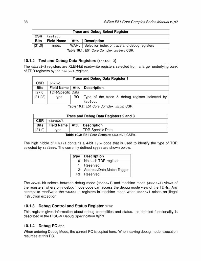
10.1.1 Trace and Debug Register Select (tselect) . . . . . . . . . . . . . . . . 37
10.1.2 Test and Debug Data Registers (tdata1–3) . . . . . . . . . . . . . . . . 38
10.1.3 Debug Control and Status Register dcsr . . . . . . . . . . . . . . . . . . 38
10.1.4 Debug PC dpc . . . . . . . . . . . . . . . . . . . . . . . . . . . . . . . . 38
10.1.5 Debug Scratch dscratch . . . . . . . . . . . . . . . . . . . . . . . . . . 39
10.2 Breakpoints . . . . . . . . . . . . . . . . . . . . . . . . . . . . . . . . . . . . . . . 39
10.2.1 Breakpoint Match Control Register mcontrol . . . . . . . . . . . . . . . 39
10.2.2 Breakpoint Match Address Register (maddress) . . . . . . . . . . . . . . 41
10.2.3 Breakpoint Execution . . . . . . . . . . . . . . . . . . . . . . . . . . . . . 41
10.2.4 Sharing breakpoints between debug and machine mode . . . . . . . . . 41
10.2.5 Sharing breakpoints between debug and machine mode . . . . . . . . . 41
10.3 Debug Memory Map . . . . . . . . . . . . . . . . . . . . . . . . . . . . . . . . . . 41
10.3.1 Debug RAM & Program Buffer (0x300–0x3FF) . . . . . . . . . . . . . . . 41
10.3.2 Debug ROM (0x800–0xFFF) . . . . . . . . . . . . . . . . . . . . . . . . . 42
10.3.3 Debug Flags (0x100 – 0x110, 0x400 – 0x7FF) . . . . . . . . . . . . . . . 42
10.3.4 Safe Zero Address . . . . . . . . . . . . . . . . . . . . . . . . . . . . . . 42
11 Debug Interface 43
11.1 JTAG TAPC State Machine . . . . . . . . . . . . . . . . . . . . . . . . . . . . . . . 44
11.2 Resetting JTAG logic . . . . . . . . . . . . . . . . . . . . . . . . . . . . . . . . . . 44
11.2.1 JTAG Clocking . . . . . . . . . . . . . . . . . . . . . . . . . . . . . . . . 44
11.2.2 JTAG Standard Instructions . . . . . . . . . . . . . . . . . . . . . . . . . 45
11.3 JTAG Debug Commands . . . . . . . . . . . . . . . . . . . . . . . . . . . . . . . . 45
11.4 Using Debug Outputs . . . . . . . . . . . . . . . . . . . . . . . . . . . . . . . . . . 45
12 References 47

vi SiFive E51 Core Complex Series Manual v1p2
Chapter 1
Introduction
SiFive’s E51 Core Complex is a high performance implementation of the RISC-V RV64IMAC archi-tecture. The SiFive E51 Core Complex is guaranteed to be compatible with all applicable RISC-Vstandards, and this document should be read together with the official RISC-V user-level, privi-leged, and external debug architecture specifications.
A summary of features in the E51 Core Complex can be found in Table 1.1.
E51 Core Complex Feature SetFeature DescriptionNumber of Harts 1 Hart.RISC-V Core Name 1x E51 RISC-V core(s).Local Interrupts 16 Local Interrupt signals per hart which can be connected to off
core complex devices.PLIC Interrupts 511 Interrupt signals which can be connected to off core complex
devices.PLIC Priority Levels The PLIC supports 7 priority levels.Hardware Breakpoints 2 hardware breakpoints.Physical Memory ProtectionUnit
PMP with 8x regions and a minimum granularity of 4 bytes.
Table 1.1: E51 Core Complex Feature Set
1.1 SiFive E51 Core Complex OverviewAn overview of the SiFive E51 Core Complex is shown in Figure 1.1. This RISC-V Core IP includesa 64-bit RISC-V microcontroller core, memory interfaces including an instruction cache as well asinstruction and data tightly integrated memory, local and global interrupt support, physical mem-ory protection, a debug unit, outgoing external TileLink platform ports, and an incoming TileLinkmaster port.
1
2 SiFive E51 Core Complex Series Manual v1p2
E31 CoreE51 Core
16KB I-Cache 64KB DTIMDebug
Physical Memory Protection
Local Interrupts
JTAG/DTM
TileLink Bus Matrix
64bit TileLink-UHw/ optional AMBA
Bridges
32bit TileLink-ULw/ optional AMBA
Bridges
64bit TileLink-UHw/ optional AMBA
Bridges
System Port Peripheral Port Front Port
CLINT
PLICGlobal Interrupts
Figure 1.1: E51 Core Complex Block Diagram.

Copyright c© 2016-2017, SiFive Inc. All rights reserved. 3
The E51 Core Complex interfaces are detailed in Chapter 4 and the memory map is detailed inChapter 5.
1.2 RISC-V CoreThe E51 Core Complex includes a 64-bit E51 RISC-V core, which is a high-performance single-issue in-order execution pipeline, with a peak sustainable execution rate of one instruction perclock cycle. The core supports Machine and User privilege modes as well as the standard Multiply,Atomic, and Compressed RISC-V extensions (RV64IMAC).
The RISC-V core is described in more detail in Chapter 3.
1.3 Memory SystemThe E51 Core Complex memory system has Tightly Integrated Instruction and Data Memory sub-systems optimized for high performance. The instruction subsystem consists of a 16 KiB 2-wayinstruction cache with the ability to reconfigure a single way into a fixed-address tightly integratedmemory. The data subsystem allows for a maximum DTIM size of 64 KiB.
The memory system is described in more detail in Chapter 3.
1.4 InterruptsThe E51 Core Complex supports 16 high-priority, low-latency local vectored interrupts per-hart.This Core Complex includes a RISC-V standard platform-level interrupt controller (PLIC), whichsupports 511 global interrupts with 7 priority levels. This Core Complex also provides the standardRISC-V machine-mode timer and software interrupts via the Core Local Interruptor (CLINT).
Interrupts are described in Chapter 6, the PLIC in Chapter 7, and the CLINT in Chapter 8.
1.5 Debug SupportThe E51 Core Complex provides external debugger support over an industry-standard JTAG port,including 2 hardware-programmable breakpoints. Debug support is described in detail in Chap-ter 10 and the debug interface is described in Chapter 11.
1.6 External TileLink InterfacesThe E51 Core Complex has two TileLink platform ports; the System and Peripheral Ports. TheSystem Port conforms to the TileLink TL-UH specification and can be used to access high-speedoff core complex devices such as main memory. The System Port supports burst accesses toaccelerate cache refills and DMA transfers. The Peripheral Port conforms to the TileLink TL-ULspecification with support for atomic operations and is typically used to access peripheral devices.
There is also a TileLink master port, called the Front Port, which allows off core complex mastersto access on core complex devices, such as the data and instruction tightly integrated memories.
More details on the TileLink interfaces can be found in Chapter 4.

4 SiFive E51 Core Complex Series Manual v1p2

Chapter 2
Terminology
CLINT Core Local Interruptor. Generates per-hart software interrupts and timerinterrupts.
Hart HARdware ThreadDTIM Data Tightly Integrated MemoryITIM Instruction Tightly Integrated MemoryJTAG Joint Test Action GroupLIM Loosely Integrated Memory. Used to describe memory space delivered in
a SiFive Core Complex but not tightly integrated to a CPU core.PMP Physical Memory ProtectionPLIC Platform-Level Interrupt Controller. The global interrupt controller in a RISC-
V system.TileLink A free and open interconnect standard originally developed at UC Berkeley.RO Used to describe a Read Only register field.RW Used to describe a Read/Write register field.WO Used to describe a Write Only registers field.WARL Write-Any Read-Legal field. A register field that can be written with any
value, but returns only supported values when read.WIRI Writes-Ignored, Reads-Ignore field. A read-only register field reserved for
future use. Writes to the field are ignored, and reads should ignore thevalue returned.
WLRL Write-Legal, Read-Legal field. A register field that should only be writtenwith legal values and that only returns legal value if last written with a legalvalue.
WPRI Writes-Preserve Reads-Ignore field. A register field that may contain un-known information. Reads should ignore the value returned, but writes tothe whole register should preserve the original value.
5

6 SiFive E51 Core Complex Series Manual v1p2
Chapter 3
E51 RISC-V Core
This chapter describes the 64-bit E51 RISC-V processor core used in the E51 Core Complex. Theprocessor core comprises an instruction memory system, an instruction fetch unit, an executionpipeline, a data memory system, and support for local interrupts.
The E51 feature set is summarized in Table 3.1.
E51 Feature SetFeature DescriptionISA RV64IMAC.Instruction Cache 16 KiB 2-way instruction cache.Instruction Tightly IntegratedMemory
The E51 has support for an ITIM with a maximumsize of 8 KiB.
Data Tightly Integrated Mem-ory
64 KiB DTIM.
Modes The E51 supports the following modes: MachineMode, User Mode.
Table 3.1: E51 Feature Set
3.1 Instruction Memory SystemThe instruction memory system consists of a dedicated 16 KiB 2-way set-associative instructioncache. The access latency of all blocks in the instruction memory system is one clock cycle.The instruction cache is not kept coherent with the rest of the platform memory system. Writes toinstruction memory must be synchronized with the instruction fetch stream by executing a FENCE.Iinstruction.
The instruction cache has a line size of 64 B and a cache line fill will trigger a burst access outsideof the E51 Core Complex. The core will cache instructions from executable addresses, with theexception of the ITIM, which is further described in Section 3.1.1. Please see the E51 CoreComplex Memory Map in Chapter 5 for a description of executable address regions which aredenoted by the attribute X.
Trying to execute an instruction from a non-executable address will result in a synchronous trap.
7
8 SiFive E51 Core Complex Series Manual v1p2
3.1.1 I-Cache ReconfigurabilityThe instruction cache can be partially reconfigured into an Instruction Tightly Integrated Mem-ory (ITIM), which occupies a fixed address range in the memory map. ITIM provides high-performance, predictable instruction delivery. Fetching an instruction from ITIM is as fast as aninstruction-cache hit, with no possibility of a cache miss. ITIM can hold data as well as instructions,though loads and stores to ITIM are not as performant as loads and stores to DTIM.
The instruction cache can be configured as ITIM for all ways except for 1 in units of cache lines(64 B bytes). A single instruction cache way must remain an instruction cache. ITIM is allocatedsimply by storing to it. A store to the nth byte of the ITIM memory map reallocates the first n + 1bytes of instruction cache as ITIM, rounded up to the next cache line.
ITIM is deallocated by storing zero to the first byte after the ITIM region, i.e. 8 KiB after the baseaddress of ITIM as indicated in the Memory Map in Chapter 5. The deallocated ITIM space isautomatically returned to the instruction cache.
For determinism, software must clear the contents of ITIM after allocating it. It is unpredictablewhether ITIM contents are preserved between deallocation and allocation.
3.2 Instruction Fetch UnitThe E51 instruction fetch unit contains branch prediction hardware to improve performance ofthe processor core. The branch predictor comprises a 40-entry branch target buffer (BTB) whichpredicts the target of taken branches, a 128-entry branch history table (BHT), which predicts thedirection of conditional branches, and a 2-entry return-address stack (RAS) which predicts thetarget of procedure returns. The branch predictor has a one-cycle latency, so that correctly pre-dicted control-flow instructions result in no penalty. Mispredicted control-flow instructions incur athree-cycle penalty.
The E51 implements the standard Compressed (C) extension to the RISC-V architecture whichallows for 16-bit RISC-V instructions.
3.3 Execution PipelineThe E51 execution unit is a single-issue, in-order pipeline. The pipeline comprises five stages:instruction fetch, instruction decode and register fetch, execute, data memory access, and registerwriteback.
The pipeline has a peak execution rate of one instruction per clock cycle, and is fully bypassed sothat most instructions have a one-cycle result latency. There are several exceptions:
• LW has a two-cycle result latency, assuming a cache hit.
• LH, LHU, LB, and LBU have a three-cycle result latency, assuming a cache hit.
• CSR reads have a three-cycle result latency.
• MUL, MULH, MULHU, and MULHSU have a 5-cycle result latency.
• DIV, DIVU, REM, and REMU have between a 2-cycle and 33-cycle result latency, dependingon the operand values.

Copyright c© 2016-2017, SiFive Inc. All rights reserved. 9
The pipeline only interlocks on read-after-write and write-after-write hazards, so instructions maybe scheduled to avoid stalls.
The E51 implements the standard Multiply (M) extension to the RISC-V architecture for integermultiplication and division. The E51 has a 8-bit per cycle hardware multiply and a 1-bit per cyclehardware divide.
Branch and jump instructions transfer control from the memory access pipeline stage. Correctly-predicted branches and jumps incur no penalty, whereas mispredicted branches and jumps incura three-cycle penalty.
Most CSR writes result in a pipeline flush with a five-cycle penalty.
3.4 Data Memory SystemThe E51 Core Complex data memory system has a tightly integrated data memory (DTIM) inter-face which supports up to 64 KiB. The access latency is two clock cycles for full words and threeclock cycles for smaller quantities. Misaligned accesses are not supported in hardware and resultin a trap to allow software emulation.
Stores are pipelined and commit on cycles where the data memory system is otherwise idle. Loadsto addresses currently in the store pipeline result in a five-cycle penalty.
3.5 Atomic Memory OperationsThe E51 core supports the RISC-V standard Atomic (A) extension on the DTIM and the PeripheralPort. Atomic memory operations to regions that do not support them generate an access exceptionprecisely at the core.
The load-reserved and store-conditional instructions are only supported on cached regions, hencegenerate an access exception on DTIM and other uncached memory regions.
See The RISC-V Instruction Set Manual, Volume I: User-Level ISA, Version 2.1 [1] for more infor-mation on the instructions added by this extension.
3.6 Local InterruptsThe E51 supports up to 16 local interrupt sources that are routed directly to the core. See Chap-ter 6 for a detailed description of Local Interrupts.
3.7 Supported ModesThe E51 supports RISC-V user-mode, providing two levels of privilege: machine (M) and user (U).U-mode provides a mechanism to isolate application processes from each other and from trustedcode running in M-mode.
See The RISC-V Instruction Set Manual, Volume II: Privileged Architecture, Version 1.10 [2] formore information on the privilege modes.
3.8 Physical Memory Protection (PMP)The E51 Core Complex includes a Physical Memory Protection Unit compliant with The RISC-VInstruction Set Manual, Volume II: Privileged Architecture, Version 1.10 [2]. PMP can be used to

10 SiFive E51 Core Complex Series Manual v1p2
set memory access privileges (read, write, execute) for specified memory regions. The E51 CoreComplex PMP supports 8 regions with a minimum region size of 4 bytes.
See Chapter 9 for more information on the PMP.
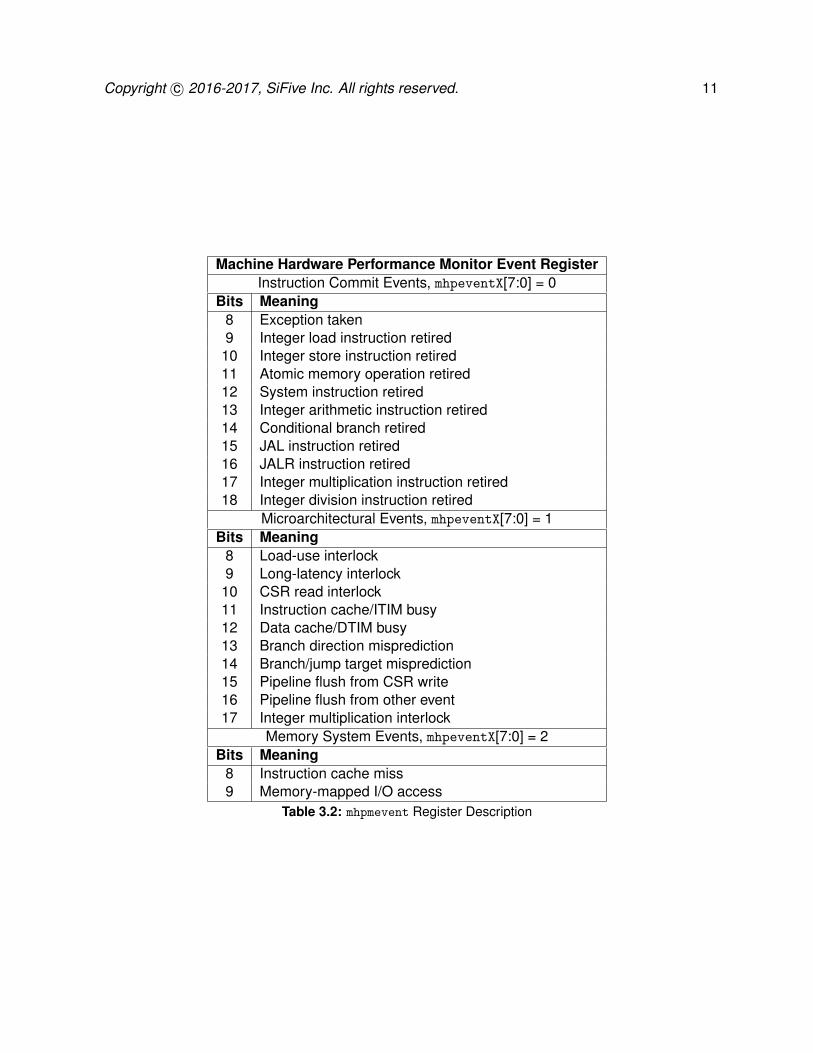
3.9 Hardware Performance MonitorThe E51 Core Complex supports a basic hardware performance monitoring facility compliant withThe RISC-V Instruction Set Manual, Volume II: Privileged Architecture, Version 1.10 [2]. Themcycle CSR holds a count of the number of clock cycles the hart has executed since some ar-bitrary time in the past. The minstret CSR holds a count of the number of instructions the harthas retired since some arbitrary time in the past. Both are 64-bit counters. The hardware per-formance monitor includes two additional event counters, mhpmcounter3 and mhpmcounter4. Theevent selector CSRs mhpmevent3 and mhpmevent4 are registers that control which event causesthe corresponding counter to increment. The mhpmcounters are 40-bit counters.
The event selectors are partitioned into two fields, as shown in Table 3.2: the lower 8 bits selectan event class, and the upper bits form a mask of events in that class. The counter increments ifthe event corresponding to any set mask bit occurs. For example, if mhpmevent3 is set to 0x4200,then mhpmcounter3 will increment when either a load instruction or a conditional branch instructionretires. Note, an event selector of 0 means “count nothing.”
Copyright c© 2016-2017, SiFive Inc. All rights reserved. 11
Machine Hardware Performance Monitor Event RegisterInstruction Commit Events, mhpeventX[7:0] = 0
Bits Meaning8 Exception taken9 Integer load instruction retired
10 Integer store instruction retired11 Atomic memory operation retired12 System instruction retired13 Integer arithmetic instruction retired14 Conditional branch retired15 JAL instruction retired16 JALR instruction retired17 Integer multiplication instruction retired18 Integer division instruction retired
Microarchitectural Events, mhpeventX[7:0] = 1Bits Meaning
8 Load-use interlock9 Long-latency interlock
10 CSR read interlock11 Instruction cache/ITIM busy12 Data cache/DTIM busy13 Branch direction misprediction14 Branch/jump target misprediction15 Pipeline flush from CSR write16 Pipeline flush from other event17 Integer multiplication interlock
Memory System Events, mhpeventX[7:0] = 2Bits Meaning
8 Instruction cache miss9 Memory-mapped I/O access
Table 3.2: mhpmevent Register Description

12 SiFive E51 Core Complex Series Manual v1p2
Chapter 4
E51 Core Complex Interfaces
This chapter describes the primary interfaces to the E51 Core Complex.
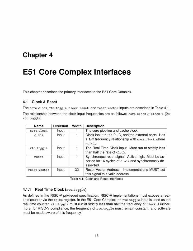
4.1 Clock & ResetThe core clock, rtc toggle, clock, reset, and reset vector inputs are described in Table 4.1.
The relationship between the clock input frequencies are as follows: core clock ≥ clock > (2×rtc toggle)
Name Direction Width Descriptioncore clock Input 1 The core pipeline and cache clock.
clock Input 1 Clock input to the PLIC, and the external ports. Hasa 1/m frequency relationship with core clock wherem ≥ 1.
rtc toggle Input 1 The Real Time Clock input. Must run at strictly lessthan half the rate of clock.
reset Input 1 Synchronous reset signal. Active high. Must be as-serted for 16 cycles of clock and synchronously de-asserted.
reset vector Input 32 Reset Vector Address. Implementations MUST setthis signal to a valid address.
Table 4.1: Clock and Reset Interfaces
4.1.1 Real Time Clock (rtc toggle)As defined in the RISC-V privileged specification, RISC-V implementations must expose a real-time counter via the mtime register. In the E51 Core Complex the rtc toggle input is used as thereal-time counter. rtc toggle must run at strictly less than half the frequency of clock. Further-more, for RISC-V compliance, the frequency of rtc toggle must remain constant, and softwaremust be made aware of this frequency.
13
14 SiFive E51 Core Complex Series Manual v1p2
4.1.2 Peripheral Clock (clock)The peripheral clock is used to decouple the frequency of the core from that of some of the oncore complex peripherals. clock has a 1/m frequency relationship with core clock where m isany positive integer. Additionally, these clocks must be phase-aligned.
The peripherals connected to clock are: PLIC, Debug, periph port tl 0, sys port tl 0, andfront port tl 0.
4.2 PortsThis section will describe all of the Ports in the E51 Core Complex.
4.2.1 TileLink Platform PortsThe E51 Core Complex has two platform ports: the System Port and the Peripheral Port. The E51Core Complex will route read and write requests from the hart to the appropriate port based onthe physical address. The E51 Core Complex supports a maximum of 7 outstanding transactions.
The E51 Core Complex ignores TileLink errors that propagate to the processor.
4.2.2 TileLink Front PortThe E51 Core Complex also has a TileLink master port interface called Front Port. This port canbe used by external masters to read and write into the local E51 Core Complex 64 KiB DTIM andto the 8 KiB ITIM memory space. Note that an external master using the Front Port can trigger theI-Cache to reconfigure itself by using the procedure described in Section 3.1.1.
Reads and writes to the front port interface can also pass through to the System and Peripheralbus interfaces if a transaction falls within their address space. Note that transactions through thefront port do not pass through the PMP.
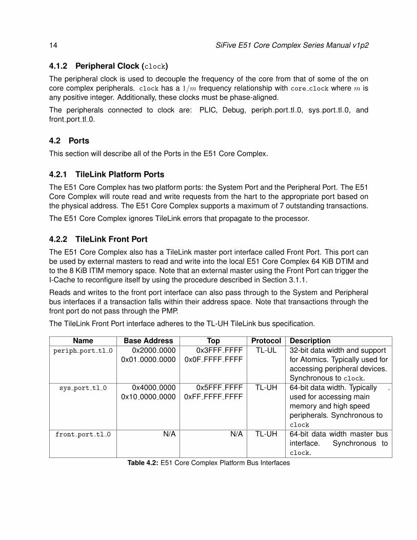
The TileLink Front Port interface adheres to the TL-UH TileLink bus specification.
Name Base Address Top Protocol Descriptionperiph port tl 0 0x2000 0000 0x3FFF FFFF TL-UL 32-bit data width and support
for Atomics. Typically used foraccessing peripheral devices.Synchronous to clock.
0x01 0000 0000 0x0F FFFF FFFF
sys port tl 0 0x4000 0000 0x5FFF FFFF TL-UH 64-bit data width. Typicallyused for accessing mainmemory and high speedperipherals. Synchronous toclock
.0x10 0000 0000 0xFF FFFF FFFF
front port tl 0 N/A N/A TL-UH 64-bit data width master businterface. Synchronous toclock.
Table 4.2: E51 Core Complex Platform Bus Interfaces

Copyright c© 2016-2017, SiFive Inc. All rights reserved. 15
4.3 Local InterruptsLocal interrupts are interrupts which can be connected to peripheral sources and signaled directlyto an individual hart. Please see Chapter 6 for a detailed description of the E51 Core Complexlocal interrupts.
Name Direction Width Descriptionlocal interrupts 0 Input 16 Interrupts from peripheral sources. These are level-
based interrupt signals connected directly to the coreand must be synchronous with core clock.
Table 4.3: Local Interrupt Interface
4.4 Global InterruptsGlobal interrupts are interrupts which are connected to the PLIC from peripheral sources. Pleasesee Chapter 7 for a detailed description of the E51 Core Complex PLIC.
Name Direction Width Descriptionglobal interrupts Input 511 External interrupts from off-chip or peripheral
sources. These are level-based interrupt signalsconnected to the PLIC and must be synchronouswith clock.
Table 4.4: External Interrupt Interface
4.5 DTIM SizingIt is possible to implement less than the maximum specified 64 KiB DTIM. When doing so, boot-time software must program a Locked PMP region spanning the unimplemented address space toguarantee that accesses to unimplemented memory space are trapped accordingly. Please seeChapter 9 for more details on how to configure PMP.
4.6 Debug Output SignalsSignals which are outputs from the Debug Module are shown in Table 4.5.
Name Direction Width Descriptiondebug ndreset Output 1 This signal is a reset signal driven by the De-
bug Logic of the chip. It can be used to resetparts of the SoC or the entire chip. It shouldNOT be wired into logic which feeds back into thedebug systemjtag reset signal for this block. Thissignal may be left unconnected.
debug dmactive Output 1 This signal, 0 at reset, indicates that debug logic isactive. This may be used to prevent power gating ofdebug logic, etc. It may be left unconnected.
Table 4.5: External Debug Logic Control Pins

16 SiFive E51 Core Complex Series Manual v1p2
4.7 JTAG Debug Interface PinoutSiFive uses the industry-standard JTAG interface which includes the four standard signals, TCK,TMS, TDI, and TDO. A test logic reset signal must also be driven on the debug systemjtag reset
input. This reset is synchronized internally to the design. The test logic reset must be pulsedbefore the core reset is deasserted.
Name Direction Width Descriptiondebug systemjtag TCK Input 1 JTAG Test Clockdebug systemjtag TMS Input 1 JTAG Test Mode Selectdebug systemjtag TDI Input 1 JTAG Test Data Input
debug systemjtag TDO data Output 1 JTAG Test Data Outputdebug systemjtag TDO driven Output 1 JTAG Test Data Output Enable
debug systemjtag reset Input 1 Active-high Resetdebug systemjtag mfr id Input 11 The SoC Manufacturer ID which will
be reported by the JTAG IDCODE in-struction.
Table 4.6: SiFive standard JTAG interface for off-chip external TAPC and on-chip embedded TAPC.
Chapter 5
Memory Map
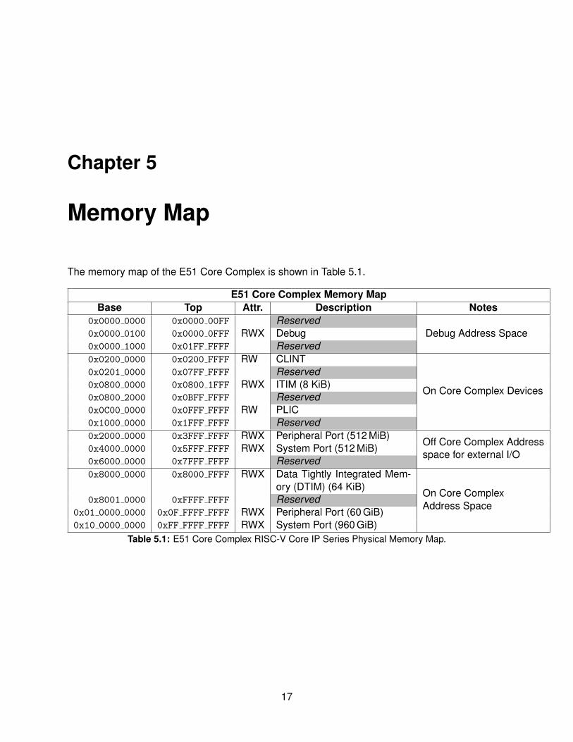
The memory map of the E51 Core Complex is shown in Table 5.1.
E51 Core Complex Memory MapBase Top Attr. Description Notes
0x0000 0000 0x0000 00FF ReservedDebug Address Space0x0000 0100 0x0000 0FFF RWX Debug
0x0000 1000 0x01FF FFFF Reserved0x0200 0000 0x0200 FFFF RW CLINT
On Core Complex Devices
0x0201 0000 0x07FF FFFF Reserved0x0800 0000 0x0800 1FFF RWX ITIM (8 KiB)0x0800 2000 0x0BFF FFFF Reserved0x0C00 0000 0x0FFF FFFF RW PLIC0x1000 0000 0x1FFF FFFF Reserved0x2000 0000 0x3FFF FFFF RWX Peripheral Port (512 MiB)
Off Core Complex Addressspace for external I/O
0x4000 0000 0x5FFF FFFF RWX System Port (512 MiB)0x6000 0000 0x7FFF FFFF Reserved0x8000 0000 0x8000 FFFF RWX Data Tightly Integrated Mem-
ory (DTIM) (64 KiB)On Core ComplexAddress Space
0x8001 0000 0xFFFF FFFF Reserved0x01 0000 0000 0x0F FFFF FFFF RWX Peripheral Port (60 GiB)0x10 0000 0000 0xFF FFFF FFFF RWX System Port (960 GiB)
Table 5.1: E51 Core Complex RISC-V Core IP Series Physical Memory Map.
17

18 SiFive E51 Core Complex Series Manual v1p2
Chapter 6
Interrupts
This chapter describes how interrupt concepts in the RISC-V architecture apply to the E51 CoreComplex. The definitive resource for information about the RISC-V interrupt architecture is TheRISC-V Instruction Set Manual, Volume II: Privileged Architecture, Version 1.10 [2].
6.1 Interrupt ConceptsEach hart in SiFive RISC-V Core IP has support for the following interrupts: local (including soft-ware and timer), and global.
Local interrupts are signaled directly to an individual hart with a dedicated interrupt value. Thisallows for reduced interrupt latency as there is no arbitration required to determine which hart willservice a given request, nor additional memory accesses required to determine the cause of theinterrupt. Software and timer interrupts are local interrupts generated by the Core Local Interruptor(CLINT).
Global interrupts by contrast, are routed through a Platform-Level Interrupt Controller (PLIC), whichcan direct interrupts to any hart in the system via the external interrupt. Decoupling global inter-rupts from the hart(s) allows the design of the PLIC to be tailored to the platform, permitting abroad range of attributes like the number of interrupts and the prioritization and routing schemes.
This chapter describes the E51 Core Complex interrupt architecture. Chapter 7 describes theglobal interrupt architecture and the PLIC design. Chapter 8 describes the Core Local Interruptor.
The E51 Core Complex interrupt architecture is depicted in Figure 6.1.
19

20 SiFive E51 Core Complex Series Manual v1p2
SiFive Core Complex Boundry
...
hart 0
Machine Software Interrupt
Machine Timer Interrupt
Local Interrupt 0
Local Interrupt X
PLIC
Global Interrupts
CLINT
Machine External Interrupt
Figure 6.1: E51 Core Complex Interrupt Architecture Block Diagram.
6.2 Interrupt Entry and ExitWhen a RISC-V hart takes an interrupt the following will occur:
• The value of mstatus.MIE is copied into mstatus.MPIE, then mstatus.MIE is cleared, effec-tively disabling interrupts.
• The current pc is copied into the mepc register, and then pc is set to the value of mtvec. In thecase where vectored interrupts are enabled, pc is set to mtvec.BASE + 4×exception code.
• The privilege mode prior to the interrupt is encoded in mstatus.MPP.
At this point control is handed over to software in the interrupt handler with interrupts disabled. In-terrupts can be re-enabled by explicitly setting mstatus.MIE, or by executing an MRET instructionto exit the handler. When an MRET instruction is executed, the following will occur:
• The privilege mode is set to the value encoded in mstatus.MPP.
• The value of mstatus.MPIE is copied into mstatus.MIE.
• The pc is set to the value of mepc.
At this point control is handed over to software.
The Control and Status Registers involved in handling RISC-V interrupts are described in Sec-tion 6.3.

Copyright c© 2016-2017, SiFive Inc. All rights reserved. 21
6.3 Interrupt Control Status RegistersThe SiFive E51 Core Complex specific implementation of interrupt CSRs is described below. Fora complete description of RISC-V interrupt behavior and how to access CSRs, please consult TheRISC-V Instruction Set Manual, Volume II: Privileged Architecture, Version 1.10 [2].
6.3.1 Machine Status Register (mstatus)The mstatus register keeps track of and controls the hart’s current operating state includingwhether or not interrupts are enabled. A summary of the mstatus fields related to interrupts inthe E51 Core Complex is provided in Table 6.1; note that this is not a complete description ofmstatus as it contains fields unrelated to interrupts. For the full description of mstatus please con-sult the The RISC-V Instruction Set Manual, Volume II: Privileged Architecture, Version 1.10 [2].
Machine Status RegisterCSR mstatus
Bits Field Name Attr. Description[2:0] Reserved WPRI
3 MIE RW Machine Interrupt Enable[6:4] Reserved WPRI
7 MPIE RW Machine Previous Interrupt Enable[10:8] Reserved WPRI[12:11] MPP RW Machine Previous Privilege Mode
Table 6.1: E51 Core Complex mstatus register (partial)
Interrupts are enabled by setting the MIE bit in mstatus and by enabling the desired individualinterrupt in the mie register described in Section 6.3.2.
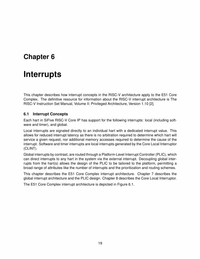
6.3.2 Machine Interrupt Enable Register (mie)Individual interrupts are enabled by setting the appropriate bit in the mie register. The E51 CoreComplex mie register is described in Table 6.2.
22 SiFive E51 Core Complex Series Manual v1p2
Machine Interrupt Enable RegisterCSR mie
Bits Field Name Attr. Description[2:0] Reserved WIRI
3 MSIE RW Machine Software Interrupt Enable[6:4] Reserved WIRI
7 MTIE RW Machine Timer Interrupt Enable[10:8] Reserved WIRI
11 MEIE RW Machine External Interrupt Enable[15:12] Reserved WPRI
16 LIE0 RW Local Interrupt 0 Enable17 LIE1 RW Local Interrupt 1 Enable18 LIE2 RW Local Interrupt 2 Enable
...31 LIE15 RW Local Interrupt 15 Enable
[63:32] Reserved WIRITable 6.2: E51 Core Complex mie register
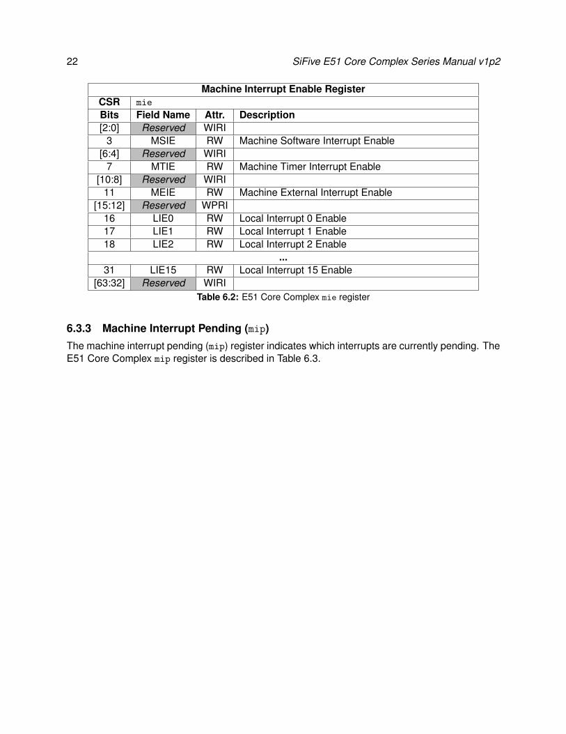
6.3.3 Machine Interrupt Pending (mip)The machine interrupt pending (mip) register indicates which interrupts are currently pending. TheE51 Core Complex mip register is described in Table 6.3.
Copyright c© 2016-2017, SiFive Inc. All rights reserved. 23
Machine Interrupt Pending RegisterCSR mip
Bits Field Name Attr. Description[2:0] Reserved WPRI
3 MSIP RO Machine Software Interrupt Pending[6:4] Reserved WPRI
7 MTIP RO Machine Timer Interrupt Pending[10:8] Reserved WPRI
11 MEIP RO Machine External Interrupt Pending[15:12] Reserved WPRI
16 LIP0 RO Local Interrupt 0 Pending17 LIP1 RO Local Interrupt 1 Pending18 LIP2 RO Local Interrupt 2 Pending
...31 LIP15 RO Local Interrupt 15 Pending
[63:32] Reserved WPRITable 6.3: E51 Core Complex mip register
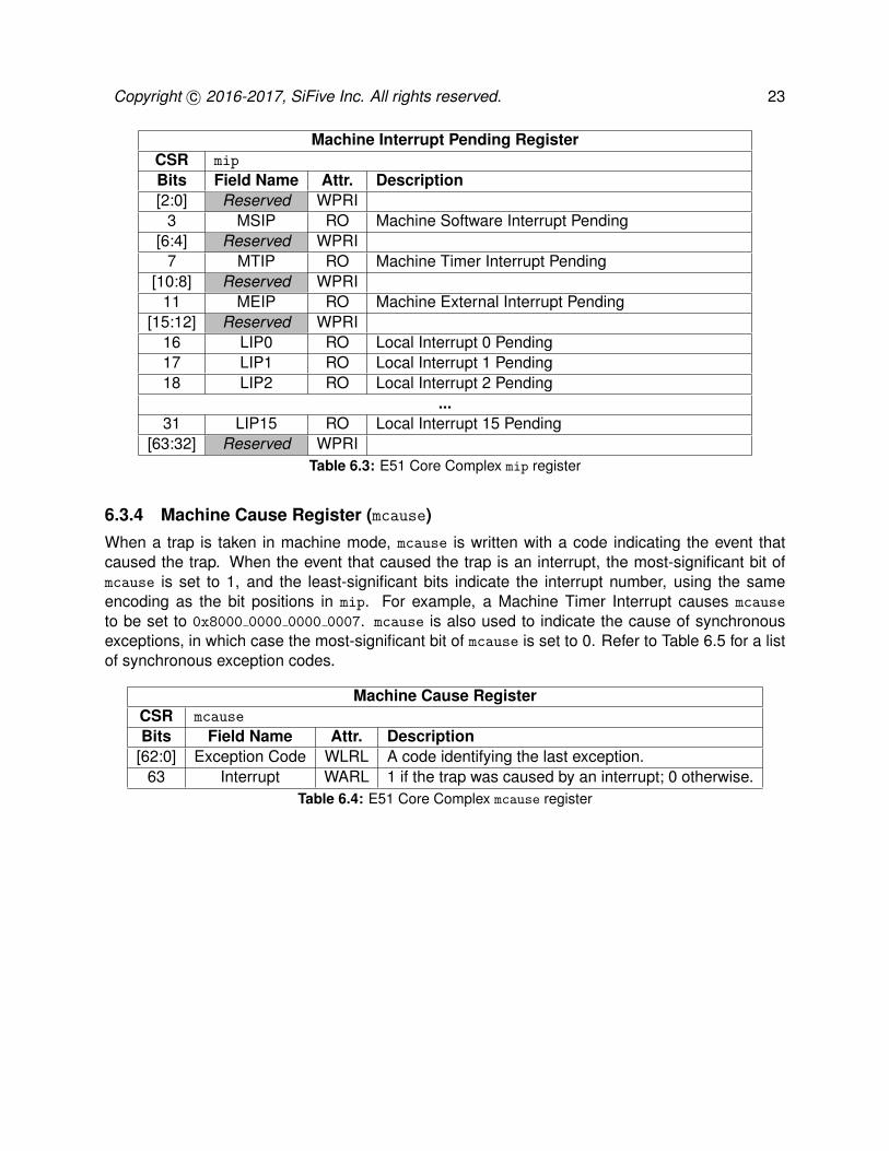
6.3.4 Machine Cause Register (mcause)When a trap is taken in machine mode, mcause is written with a code indicating the event thatcaused the trap. When the event that caused the trap is an interrupt, the most-significant bit ofmcause is set to 1, and the least-significant bits indicate the interrupt number, using the sameencoding as the bit positions in mip. For example, a Machine Timer Interrupt causes mcause
to be set to 0x8000 0000 0000 0007. mcause is also used to indicate the cause of synchronousexceptions, in which case the most-significant bit of mcause is set to 0. Refer to Table 6.5 for a listof synchronous exception codes.
Machine Cause RegisterCSR mcause
Bits Field Name Attr. Description[62:0] Exception Code WLRL A code identifying the last exception.
63 Interrupt WARL 1 if the trap was caused by an interrupt; 0 otherwise.Table 6.4: E51 Core Complex mcause register
24 SiFive E51 Core Complex Series Manual v1p2
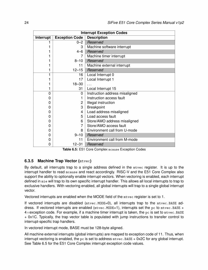
Interrupt Exception CodesInterrupt Exception Code Description
1 0–2 Reserved1 3 Machine software interrupt1 4–6 Reserved1 7 Machine timer interrupt1 8–10 Reserved1 11 Machine external interrupt1 12–15 Reserved1 16 Local Interrupt 01 17 Local Interrupt 11 18–30 . . .1 31 Local Interrupt 150 0 Instruction address misaligned0 1 Instruction access fault0 2 Illegal instruction0 3 Breakpoint0 4 Load address misaligned0 5 Load access fault0 6 Store/AMO address misaligned0 7 Store/AMO access fault0 8 Environment call from U-mode0 9–10 Reserved0 11 Environment call from M-mode0 12–31 Reserved
Table 6.5: E51 Core Complex mcause Exception Codes
6.3.5 Machine Trap Vector (mtvec)By default, all interrupts trap to a single address defined in the mtvec register. It is up to theinterrupt handler to read mcause and react accordingly. RISC-V and the E51 Core Complex alsosupport the ability to optionally enable interrupt vectors. When vectoring is enabled, each interruptdefined in mie will trap to its own specific interrupt handler. This allows all local interrupts to trap toexclusive handlers. With vectoring enabled, all global interrupts will trap to a single global interruptvector.
Vectored interrupts are enabled when the MODE field of the mtvec register is set to 1.
If vectored interrupts are disabled (mtvec.MODE=0), all interrupts trap to the mtvec.BASE ad-dress. If vectored interrupts are enabled (mtvec.MODE=1), interrupts set the pc to mtvec.BASE +4×exception code. For example, if a machine timer interrupt is taken, the pc is set to mtvec.BASE
+ 0x1C. Typically, the trap vector table is populated with jump instructions to transfer control tointerrupt-specific trap handlers.
In vectored interrupt mode, BASE must be 128-byte aligned.
All machine external interrupts (global interrupts) are mapped to exception code of 11. Thus, wheninterrupt vectoring is enabled, the pc is set to address mtvec.BASE + 0x2C for any global interrupt.See Table 6.5 for the E51 Core Complex interrupt exception code values.
Copyright c© 2016-2017, SiFive Inc. All rights reserved. 25
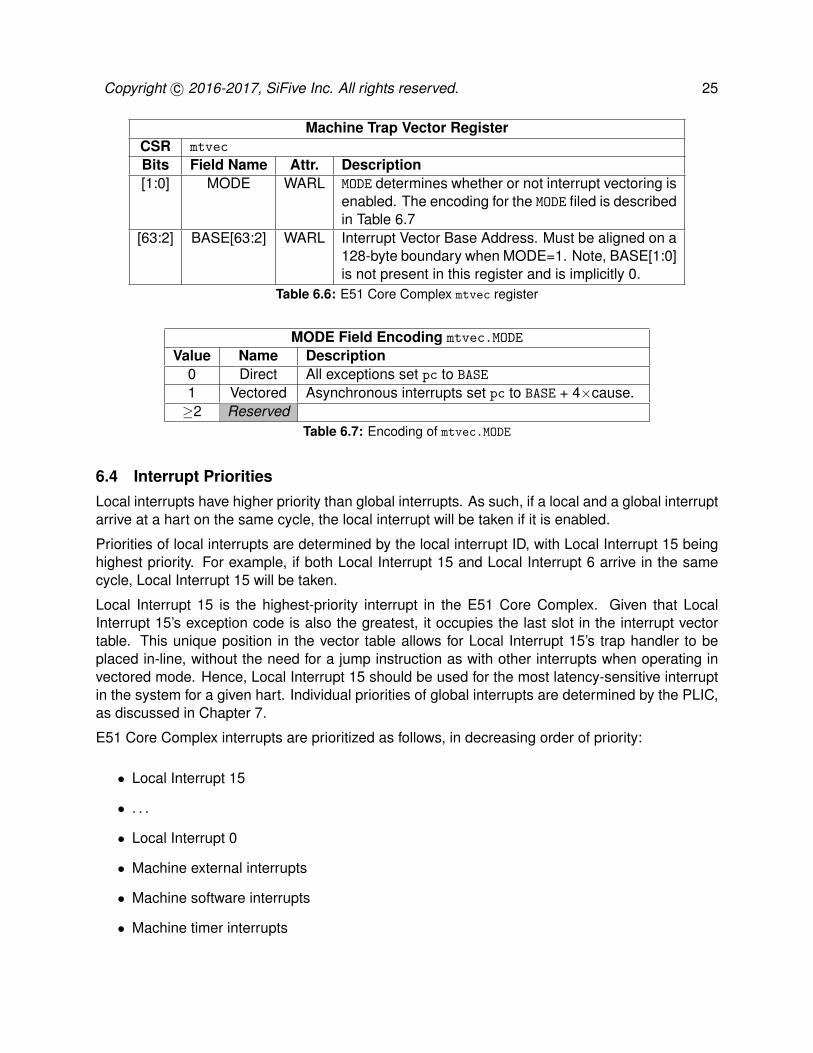
Machine Trap Vector RegisterCSR mtvec
Bits Field Name Attr. Description[1:0] MODE WARL MODE determines whether or not interrupt vectoring is
enabled. The encoding for the MODE filed is describedin Table 6.7
[63:2] BASE[63:2] WARL Interrupt Vector Base Address. Must be aligned on a128-byte boundary when MODE=1. Note, BASE[1:0]is not present in this register and is implicitly 0.
Table 6.6: E51 Core Complex mtvec register
MODE Field Encoding mtvec.MODE
Value Name Description0 Direct All exceptions set pc to BASE
1 Vectored Asynchronous interrupts set pc to BASE + 4×cause.≥2 Reserved
Table 6.7: Encoding of mtvec.MODE
6.4 Interrupt PrioritiesLocal interrupts have higher priority than global interrupts. As such, if a local and a global interruptarrive at a hart on the same cycle, the local interrupt will be taken if it is enabled.
Priorities of local interrupts are determined by the local interrupt ID, with Local Interrupt 15 beinghighest priority. For example, if both Local Interrupt 15 and Local Interrupt 6 arrive in the samecycle, Local Interrupt 15 will be taken.
Local Interrupt 15 is the highest-priority interrupt in the E51 Core Complex. Given that LocalInterrupt 15’s exception code is also the greatest, it occupies the last slot in the interrupt vectortable. This unique position in the vector table allows for Local Interrupt 15’s trap handler to beplaced in-line, without the need for a jump instruction as with other interrupts when operating invectored mode. Hence, Local Interrupt 15 should be used for the most latency-sensitive interruptin the system for a given hart. Individual priorities of global interrupts are determined by the PLIC,as discussed in Chapter 7.
E51 Core Complex interrupts are prioritized as follows, in decreasing order of priority:
• Local Interrupt 15
• . . .
• Local Interrupt 0
• Machine external interrupts
• Machine software interrupts
• Machine timer interrupts

26 SiFive E51 Core Complex Series Manual v1p2
6.5 Interrupt LatencyInterrupt latency for the E51 Core Complex, as counted by the numbers of cycles it takes fromsignaling of the interrupt to the hart to the first instruction fetch of the handler, is 4 cycles.
Global interrupts routed through the PLIC incur additional latency of 3 cycles where the PLIC isclocked by clock. This means that the total latency, in cycles, for a global interrupt is:4 + 3× (core clock Hz÷clock Hz).
This is a best case cycle count and assumes the handler is cached or located in ITIM. It does nottake into account additional latency from a peripheral source.
Additionally, the hart will not abandon a Divide instruction in flight. This means if an interrupthandler tries to use a register which is the destination register of a divide instruction, the pipelinewill stall until the divide is complete.
Chapter 7
Platform-Level Interrupt Controller(PLIC)
This chapter describes the operation of the platform-level interrupt controller (PLIC) on the SiFiveE51 Core Complex. The PLIC complies with The RISC-V Instruction Set Manual, Volume II:Privileged Architecture, Version 1.10 [2], and can support a maximum of 511 external interruptsources with 7 priority levels.
The E51 Core Complex PLIC resides is in the clock timing domain allowing for relaxed timingrequirements. The latency of global interrupts, as perceived by a hart, increases with the ratio ofthe core clock frequency and the clock frequency.
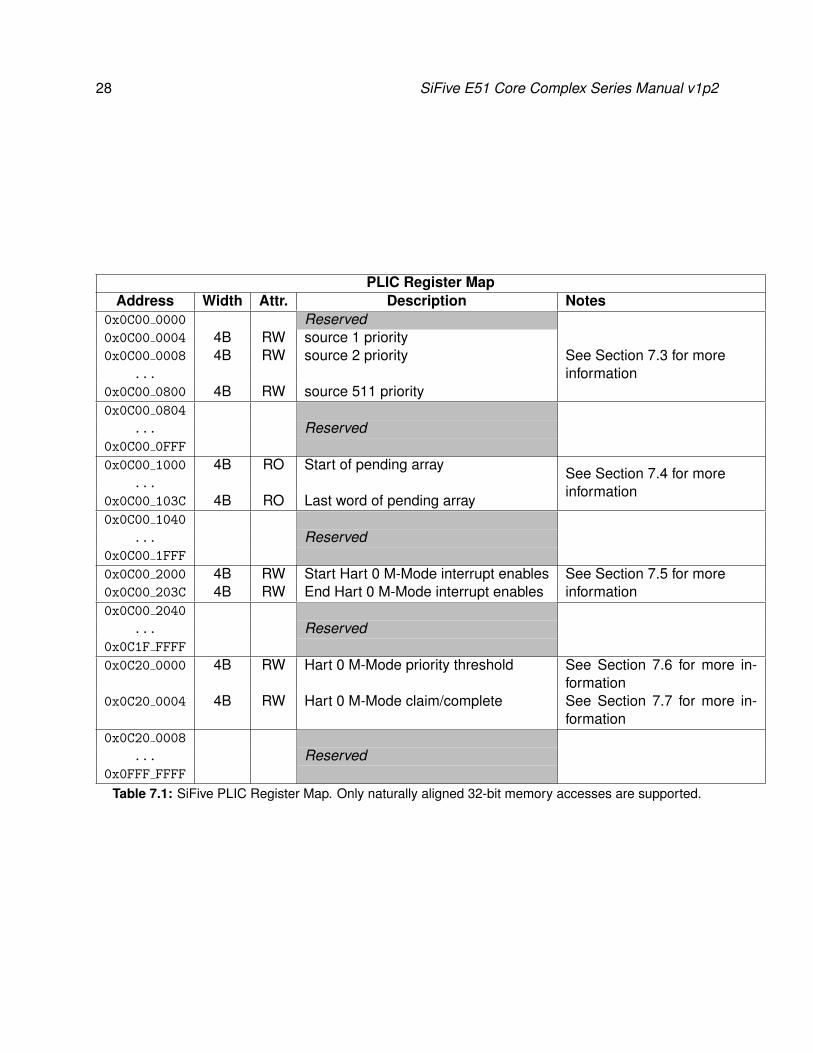
7.1 Memory MapThe memory map for the SiFive E51 Core Complex PLIC control registers is shown in Table 7.1.The PLIC memory map has been designed to only require naturally aligned 32-bit memory ac-cesses.
27
28 SiFive E51 Core Complex Series Manual v1p2
PLIC Register MapAddress Width Attr. Description Notes
0x0C00 0000 Reserved0x0C00 0004 4B RW source 1 priority
See Section 7.3 for moreinformation
0x0C00 0008 4B RW source 2 priority...
0x0C00 0800 4B RW source 511 priority0x0C00 0804
... Reserved0x0C00 0FFF
0x0C00 1000 4B RO Start of pending arraySee Section 7.4 for moreinformation
...
0x0C00 103C 4B RO Last word of pending array0x0C00 1040
... Reserved0x0C00 1FFF
0x0C00 2000 4B RW Start Hart 0 M-Mode interrupt enables See Section 7.5 for moreinformation0x0C00 203C 4B RW End Hart 0 M-Mode interrupt enables
0x0C00 2040
... Reserved0x0C1F FFFF
0x0C20 0000 4B RW Hart 0 M-Mode priority threshold See Section 7.6 for more in-formation
0x0C20 0004 4B RW Hart 0 M-Mode claim/complete See Section 7.7 for more in-formation
0x0C20 0008
... Reserved0x0FFF FFFF
Table 7.1: SiFive PLIC Register Map. Only naturally aligned 32-bit memory accesses are supported.

Copyright c© 2016-2017, SiFive Inc. All rights reserved. 29
7.2 Interrupt SourcesThe E51 Core Complex has 511 interrupt sources exposed at the top level via theglobal interrupts signals. These signals are positive-level triggered.
Any unused global interrupts inputs should be tied to logic 0.
In the PLIC, as specified in The RISC-V Instruction Set Manual, Volume II: Privileged Ar-chitecture, Version 1.10 [2], Global Interrupt ID 0 is defined to mean “no interrupt” , henceglobal interrupts[0] corresponds to PLIC Interrupt ID 1.
7.3 Interrupt PrioritiesEach PLIC interrupt source can be assigned a priority by writing to its 32-bit memory-mappedpriority register. The E51 Core Complex supports 7 levels of priority. A priority value of 0 isreserved to mean “never interrupt” and effectively dissables the interrupt. Priority 1 is the lowestactive priority, and priority 7 is the highest. Ties between global interrupts of the same priority arebroken by the Interrupt ID; interrupts with the lowest ID have the highest effective priority. Pleasesee Table 7.2 for the detailed register description.
PLIC Interrupt Priority Register (priority)Base Address 0x0C00 0000 + 4×Interrupt ID
Bits Field Name Attr. Rst. Description[2:0] Priority WARL X Sets the priority for a given global interrupt.31:3] Reserved WIRI X
Table 7.2: PLIC Interrupt Priority Registers
7.4 Interrupt Pending BitsThe current status of the interrupt source pending bits in the PLIC core can be read from thepending array, organized as 15 words of 32 bits. The pending bit for interrupt ID N is stored in bit(N mod 32) of word (N/32). As such, the E51 Core Complex has 15 interrupt pending registers.Bit 0 of word 0, which represents the non-existent interrupt source 0, is hardwired to zero.
A pending bit in the PLIC core can be cleared by setting the associated enable bit then performinga claim as as described in Section 7.7.
PLIC Interrupt Pending Register 1 (pending1)Base Address 0x0C00 1000
Bits Field Name Attr. Rst. Description0 Interrupt 0 Pending RO 0 Non-existent global interrupt 0 is hardwired to
zero1 Interrupt 1 Pending RO 0 Pending bit for global interrupt 12 Interrupt 2 Pending RO 0 Pending bit for global interrupt 2
...31 Interrupt 31 Pending RO 0 Pending bit for global interrupt 31
Table 7.3: PLIC Interrupt Pending Register 1
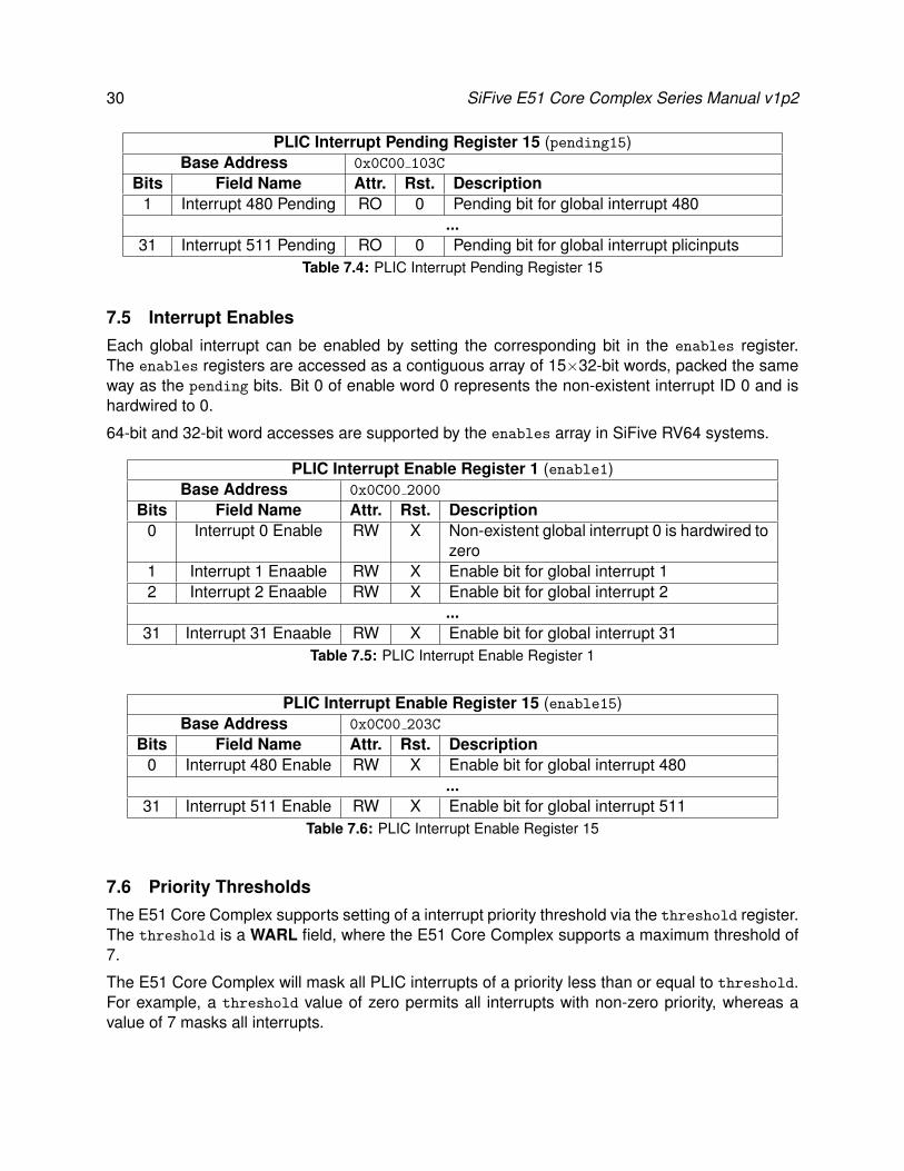
30 SiFive E51 Core Complex Series Manual v1p2
PLIC Interrupt Pending Register 15 (pending15)Base Address 0x0C00 103C
Bits Field Name Attr. Rst. Description1 Interrupt 480 Pending RO 0 Pending bit for global interrupt 480
...31 Interrupt 511 Pending RO 0 Pending bit for global interrupt plicinputs
Table 7.4: PLIC Interrupt Pending Register 15
7.5 Interrupt EnablesEach global interrupt can be enabled by setting the corresponding bit in the enables register.The enables registers are accessed as a contiguous array of 15×32-bit words, packed the sameway as the pending bits. Bit 0 of enable word 0 represents the non-existent interrupt ID 0 and ishardwired to 0.
64-bit and 32-bit word accesses are supported by the enables array in SiFive RV64 systems.
PLIC Interrupt Enable Register 1 (enable1)Base Address 0x0C00 2000
Bits Field Name Attr. Rst. Description0 Interrupt 0 Enable RW X Non-existent global interrupt 0 is hardwired to
zero1 Interrupt 1 Enaable RW X Enable bit for global interrupt 12 Interrupt 2 Enaable RW X Enable bit for global interrupt 2
...31 Interrupt 31 Enaable RW X Enable bit for global interrupt 31
Table 7.5: PLIC Interrupt Enable Register 1
PLIC Interrupt Enable Register 15 (enable15)Base Address 0x0C00 203C
Bits Field Name Attr. Rst. Description0 Interrupt 480 Enable RW X Enable bit for global interrupt 480
...31 Interrupt 511 Enable RW X Enable bit for global interrupt 511
Table 7.6: PLIC Interrupt Enable Register 15
7.6 Priority ThresholdsThe E51 Core Complex supports setting of a interrupt priority threshold via the threshold register.The threshold is a WARL field, where the E51 Core Complex supports a maximum threshold of7.
The E51 Core Complex will mask all PLIC interrupts of a priority less than or equal to threshold.For example, a threshold value of zero permits all interrupts with non-zero priority, whereas avalue of 7 masks all interrupts.
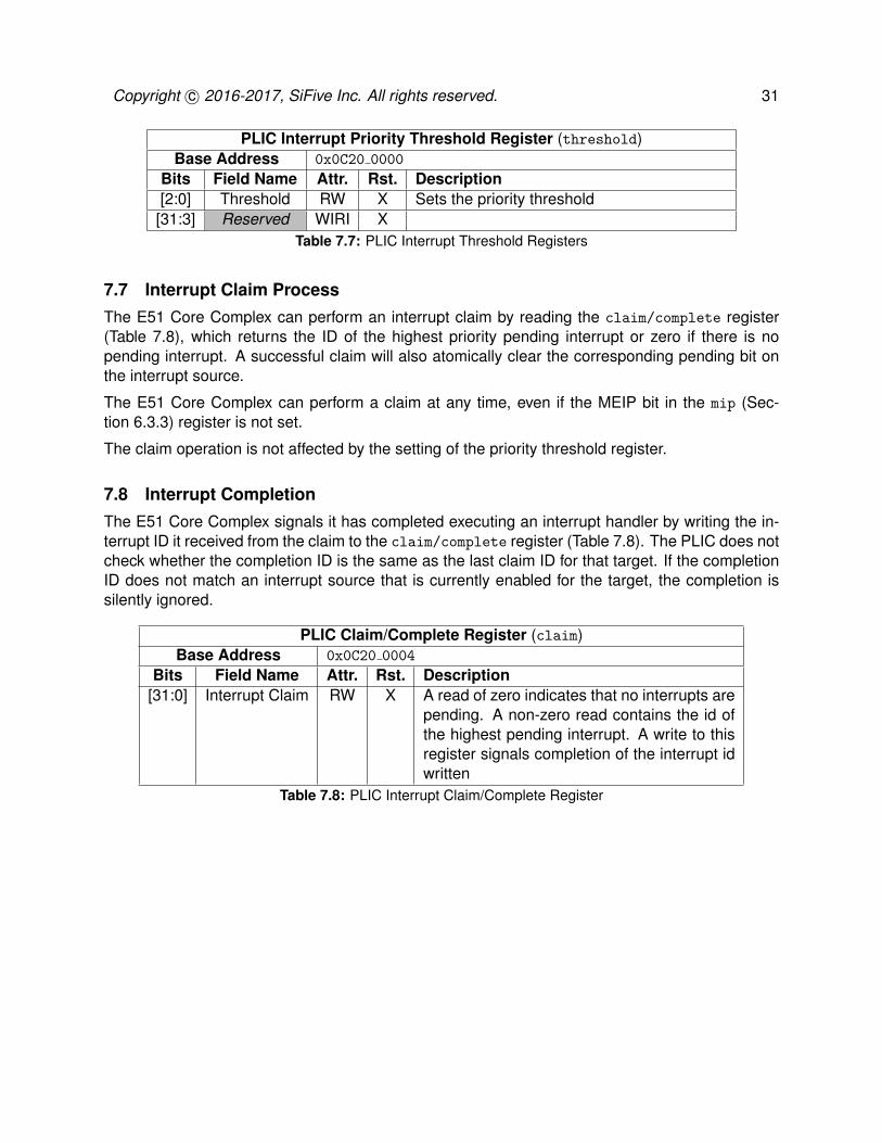
Copyright c© 2016-2017, SiFive Inc. All rights reserved. 31
PLIC Interrupt Priority Threshold Register (threshold)Base Address 0x0C20 0000
Bits Field Name Attr. Rst. Description[2:0] Threshold RW X Sets the priority threshold[31:3] Reserved WIRI X
Table 7.7: PLIC Interrupt Threshold Registers
7.7 Interrupt Claim ProcessThe E51 Core Complex can perform an interrupt claim by reading the claim/complete register(Table 7.8), which returns the ID of the highest priority pending interrupt or zero if there is nopending interrupt. A successful claim will also atomically clear the corresponding pending bit onthe interrupt source.
The E51 Core Complex can perform a claim at any time, even if the MEIP bit in the mip (Sec-tion 6.3.3) register is not set.
The claim operation is not affected by the setting of the priority threshold register.
7.8 Interrupt CompletionThe E51 Core Complex signals it has completed executing an interrupt handler by writing the in-terrupt ID it received from the claim to the claim/complete register (Table 7.8). The PLIC does notcheck whether the completion ID is the same as the last claim ID for that target. If the completionID does not match an interrupt source that is currently enabled for the target, the completion issilently ignored.
PLIC Claim/Complete Register (claim)Base Address 0x0C20 0004
Bits Field Name Attr. Rst. Description[31:0] Interrupt Claim RW X A read of zero indicates that no interrupts are
pending. A non-zero read contains the id ofthe highest pending interrupt. A write to thisregister signals completion of the interrupt idwritten
Table 7.8: PLIC Interrupt Claim/Complete Register

32 SiFive E51 Core Complex Series Manual v1p2
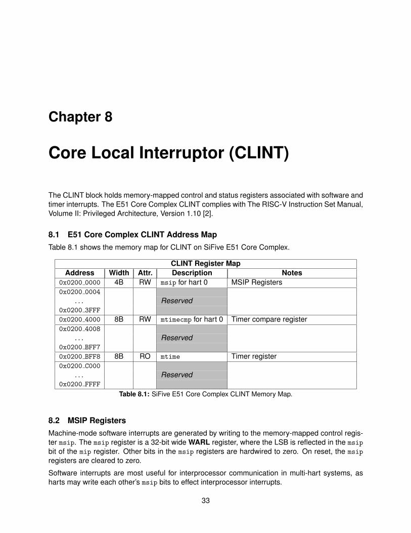
Chapter 8
Core Local Interruptor (CLINT)
The CLINT block holds memory-mapped control and status registers associated with software andtimer interrupts. The E51 Core Complex CLINT complies with The RISC-V Instruction Set Manual,Volume II: Privileged Architecture, Version 1.10 [2].
8.1 E51 Core Complex CLINT Address MapTable 8.1 shows the memory map for CLINT on SiFive E51 Core Complex.
CLINT Register MapAddress Width Attr. Description Notes
0x0200 0000 4B RW msip for hart 0 MSIP Registers0x0200 0004
. . . Reserved0x0200 3FFF
0x0200 4000 8B RW mtimecmp for hart 0 Timer compare register0x0200 4008
. . . Reserved0x0200 BFF7
0x0200 BFF8 8B RO mtime Timer register0x0200 C000
. . . Reserved0x0200 FFFF
Table 8.1: SiFive E51 Core Complex CLINT Memory Map.
8.2 MSIP RegistersMachine-mode software interrupts are generated by writing to the memory-mapped control regis-ter msip. The msip register is a 32-bit wide WARL register, where the LSB is reflected in the msip
bit of the mip register. Other bits in the msip registers are hardwired to zero. On reset, the msip
registers are cleared to zero.
Software interrupts are most useful for interprocessor communication in multi-hart systems, asharts may write each other’s msip bits to effect interprocessor interrupts.
33

34 SiFive E51 Core Complex Series Manual v1p2
8.3 Timer Registersmtime is a 64-bit read-write register that contains the number of cycles counted from thertc toggle signal described in Chapter 4. A timer interrupt is pending whenever mtime is greaterthan or equal to the value in the mtimecmp register. The timer interrupt is reflected in the mtip bitof the mip register described in Chapter 6.
On reset, mtime is cleared to zero. The mtimecmp registers are not reset.
Chapter 9
Physical Memory Protection
This chapter describes how physical memory protection concepts in the RISC-V architecture applyto the E51 Core Complex. The definitive resource for information about the RISC-V physical mem-ory protection is The RISC-V Instruction Set Manual, Volume II: Privileged Architecture, Version1.10 [2].
9.1 Functional DescriptionThe E51 Core Complex includes a Physical Memory Protection (PMP) unit, which can be used torestrict access to memory and isolate processes from each other.
The E51 Core Complex PMP unit has 8 regions and a minimum granularity of 4 bytes. It is permit-ted to have overlapping regions. The E51 Core Complex PMP unit implements the architecturallydefined pmpcfg0 CSR, supporting 8 regions. pmpcg1, pmpcfg2 and pmpcfg3 are implemented buthardwired to zero.
The PMP registers may only be programmed in M-mode. Ordinarily, the PMP unit enforces per-missions on U-mode accesses. However, locked regions (see Section 9.2) additionally enforcetheir permissions on M-mode.
9.2 Region LockingThe PMP allows for region locking whereby once a region is locked, further writes to the configura-tion and address registers are ignored. Locked PMP entries may only be unlocked with a systemreset. A region may be locked by setting the L bit in the pmpicfg register.
In addition to locking the PMP entry, the L bit indicates whether the R/W/X permissions are en-forced on M-Mode accesses. When the L bit is set, these permissions are enforced for all privilegemodes. When L bit is clear, the R/W/X permissions apply only to U-mode.
When implementing less than he maximum DTIM RAM, it is necessary to lock one PMP regionencompassing the unimplemented address space with no R/W/X permissions. Doing so will forceall access to the unimplemented address space to generate an exception.
For example, if one only implemented 32 KiB of DTIM RAM, then setting pmp0cfg=0x98 andpmpaddr0=0x2000 0FFF will disable access to the unimplemented 32 KiB region above.
35

36 SiFive E51 Core Complex Series Manual v1p2
Chapter 10
Debug
This chapter describes the operation of SiFive debug hardware, which follows the RISC-V DebugSpecification v0p13. Currently only interactive debug and hardware breakpoints are supported.
10.1 Debug CSRsThis section describes the per-hart trace and debug registers (TDRs), which are mapped into theCSR space as follows:
CSR Name Description Allowed Access Modestselect Trace and debug register select D, Mtdata1 First field of selected TDR D, Mtdata2 Second field of selected TDR D, Mtdata3 Third field of selected TDR D, Mdcsr Debug control and status register Ddpc Debug PC D
dscratch Debug scratch register D
The dcsr, dpc, and dscratch registers are only accessible in debug mode, while the tselect andtdata1–3 registers are accessible from either debug mode or machine mode.
10.1.1 Trace and Debug Register Select (tselect)To support a large and variable number of TDRs for tracing and breakpoints, they are accessedthrough one level of indirection where the tselect register selects which bank of three tdata1–3registers are accessed via the other three addresses.
The tselect register has the format shown below:
The index field is a WARL field that will not hold indices of unimplemented TDRs. Even if indexcan hold a TDR index, it does not guarantee the TDR exists. The type field of tdata1 must beinspected to determine whether the TDR exists.
37
38 SiFive E51 Core Complex Series Manual v1p2
Trace and Debug Select RegisterCSR tselect
Bits Field Name Attr. Description[31:0] index WARL Selection index of trace and debug registers
Table 10.1: E51 Core Complex tselect CSR.
10.1.2 Test and Debug Data Registers (tdata1–3)The tdata1–3 registers are XLEN-bit read/write registers selected from a larger underlying bankof TDR registers by the tselect register.
Trace and Debug Data Register 1CSR tdata1
Bits Field Name Attr. Description[27:0] TDR-Specific Data[31:28] type RO Type of the trace & debug register selected by
tselect
Table 10.2: E51 Core Complex tdata1 CSR.
Trace and Debug Data Registers 2 and 3CSR tdata2/3
Bits Field Name Attr. Description[31:0] type TDR-Specific Data
Table 10.3: E51 Core Complex tdata2/3 CSRs.
The high nibble of tdata1 contains a 4-bit type code that is used to identify the type of TDRselected by tselect. The currently defined types are shown below:
type Description0 No such TDR register1 Reserved2 Address/Data Match Trigger
≥3 Reserved
The dmode bit selects between debug mode (dmode=1) and machine mode (dmode=1) views ofthe registers, where only debug mode code can access the debug mode view of the TDRs. Anyattempt to read/write the tdata1–3 registers in machine mode when dmode=1 raises an illegalinstruction exception.
10.1.3 Debug Control and Status Register dcsrThis register gives information about debug capabilities and status. Its detailed functionality isdescribed in the RISC-V Debug Specification 0p13.
10.1.4 Debug PC dpc
When entering Debug Mode, the current PC is copied here. When leaving debug mode, executionresumes at this PC.
Copyright c© 2016-2017, SiFive Inc. All rights reserved. 39
10.1.5 Debug Scratch dscratch
This register is generally reserved for use by Debug ROM in order to save registers needed by thecode in Debug ROM. The debugger may use it as described in the RISC-V Debug Specification0p13.
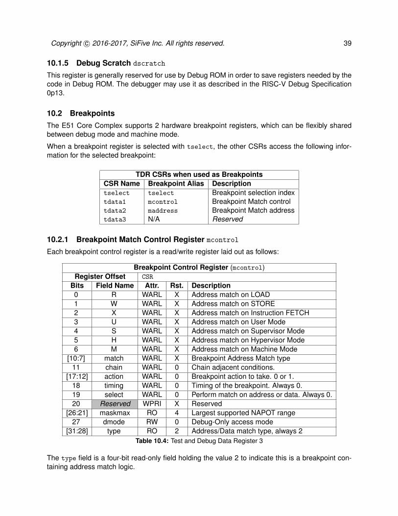
10.2 BreakpointsThe E51 Core Complex supports 2 hardware breakpoint registers, which can be flexibly sharedbetween debug mode and machine mode.
When a breakpoint register is selected with tselect, the other CSRs access the following infor-mation for the selected breakpoint:
TDR CSRs when used as BreakpointsCSR Name Breakpoint Alias Descriptiontselect tselect Breakpoint selection indextdata1 mcontrol Breakpoint Match controltdata2 maddress Breakpoint Match addresstdata3 N/A Reserved
10.2.1 Breakpoint Match Control Register mcontrolEach breakpoint control register is a read/write register laid out as follows:
Breakpoint Control Register (mcontrol)Register Offset CSR
Bits Field Name Attr. Rst. Description0 R WARL X Address match on LOAD1 W WARL X Address match on STORE2 X WARL X Address match on Instruction FETCH3 U WARL X Address match on User Mode4 S WARL X Address match on Supervisor Mode5 H WARL X Address match on Hypervisor Mode6 M WARL X Address match on Machine Mode
[10:7] match WARL X Breakpoint Address Match type11 chain WARL 0 Chain adjacent conditions.
[17:12] action WARL 0 Breakpoint action to take. 0 or 1.18 timing WARL 0 Timing of the breakpoint. Always 0.19 select WARL 0 Perform match on address or data. Always 0.20 Reserved WPRI X Reserved
[26:21] maskmax RO 4 Largest supported NAPOT range27 dmode RW 0 Debug-Only access mode
[31:28] type RO 2 Address/Data match type, always 2Table 10.4: Test and Debug Data Register 3
The type field is a four-bit read-only field holding the value 2 to indicate this is a breakpoint con-taining address match logic.

40 SiFive E51 Core Complex Series Manual v1p2
The bpaction field is an eight-bit read-write WARL field that specifies the available actions whenthe address match is successful. The value 0 generates a breakpoint exception. The value 1enters debug mode. Other actions are not implemented.
The R/W/X bits are individual WARL fields and if set, indicate an address match should only besuccessful for loads/stores/instruction fetches respectively, and all combinations of implementedbits must be supported.
The M/H/S/U bits are individual WARL fields and if set, indicate that an address match should onlybe successful in the machine/hypervisor/supervisor/user modes respectively, and all combinationsof implemented bits must be supported.
The match field is a 4-bit read-write WARL field that encodes the type of address range for break-point address matching. Three different match settings are currently supported: exact, NAPOT,and arbitrary range. A single breakpoint register supports both exact address matches andmatches with address ranges that are naturally aligned powers-of-two (NAPOT) in size. Break-point registers can be paired to specify arbitrary exact ranges, with the lower-numbered breakpointregister giving the byte address at the bottom of the range and the higher-numbered breakpointregister giving the address one byte above the breakpoint range, and using the chain bit to indicateboth must match for the action to be taken.
NAPOT ranges make use of low-order bits of the associated breakpoint address register to encodethe size of the range as follows:
NAPOT Size Encodingmaddress Match type and size
a...aaaaaa Exact 1 bytea...aaaaa0 2-byte NAPOT rangea...aaaa01 4-byte NAPOT rangea...aaa011 8-byte NAPOT rangea...aa0111 16-byte NAPOT rangea...a01111 32-byte NAPOT range
. . . . . .a01...1111 231-byte NAPOT range
The maskmax field is a 6-bit read-only field that specifies the largest supported NAPOT range. Thevalue is the logarithm base 2 of the number of bytes in the largest supported NAPOT range. Avalue of 0 indicates that only exact address matches are supported (one byte range). A value of31 corresponds to the maximum NAPOT range, which is 231 bytes in size. The largest range isencoded in maddress with the 30 least-signicant bits set to 1, bit 30 set to 0, and bit 31 holding theonly address bit considered in the address comparison.
The unary encoding of NAPOT ranges was chosen to reduce the hardware cost of storing andgenerating the corresponding address mask value.
To provide breakpoints on an exact range, two neighboring breakpoints can be combined with thechain bit. The first breakpoint can be set to match on an address using action of 2 (greater thanor equal). The second breakpoint can be set to match on address using action of 3 (less than).Setting then chain bit on the first breakpoint will then cause it prevent the second breakpoint fromfiring unless they both match.
Copyright c© 2016-2017, SiFive Inc. All rights reserved. 41
10.2.2 Breakpoint Match Address Register (maddress)Each breakpoint match address register is an XLEN-bit read/write register used to hold significantaddress bits for address matching, and also the unary-encoded address masking information forNAPOT ranges.
10.2.3 Breakpoint ExecutionBreakpoint traps are taken precisely. Implementations that emulate misaligned accesses in soft-ware will generate a breakpoint trap when either half of the emulated access falls within the ad-dress range. Implementations that support misaligned accesses in hardware must trap if any byteof an access falls within the matching range.
Debug-mode breakpoint traps jump to the debug trap vector without altering machine-mode regis-ters.
Machine-mode breakpoint traps jump to the exception vector with “Breakpoint” set in the mcause
register, and with badaddr holding the instruction or data address that caused the trap.
10.2.4 Sharing breakpoints between debug and machine modeWhen debug mode uses a breakpoint register, it is no longer visible to machine-mode (i.e., thetdrtype will be 0). Usually, the debugger will grab the breakpoints it needs before entering ma-chine mode, so machine mode will operate with the remaining breakpoint registers.
10.2.5 Sharing breakpoints between debug and machine modeWhen debug mode uses a breakpoint register, it is no longer visible to machine-mode (i.e., thetdrtype will be 0). Usually, the debugger will grab the breakpoints it needs before entering ma-chine mode, so machine mode will operate with the remaining breakpoint registers.
10.3 Debug Memory MapThis section describes the debug module’s memory map when accessed via the regular systeminterconnect. The debug module is only accessible to debug code running in debug mode on ahart (or via a debug transport module).
10.3.1 Debug RAM & Program Buffer (0x300–0x3FF)The E51 Core Complex has 16 32-bit words of Program Buffer for the debugger to direct a hartto execute arbitrary RISC-V code. Its location in memory can be determined by executing aiupc
instructions and storing the result into the Program Buffer.
The E51 Core Complex has 1 32-bit words of Debug Data RAM. Its location can be determinedby reading the DMHARTINFO register as described in the RISC-V Debug Specification. This RAMspace is used to pass data for the Access Register abstract command described in the RISC-VDebug Specification. The E51 Core Complexsupports only GPR register access when harts arehalted. All other commands must be implemented by executing from the Debug Program Buffer.
In the E51 Core Complex, both the Program Buffer and Debug Data RAM are general purposeRAM and are mapped contiguously in the RISC-V Core IP’s memory space. Therefore, additional
42 SiFive E51 Core Complex Series Manual v1p2
data can be passed in the Program Buffer and additional instructions can be stored in the DebugData RAM.
Debuggers must not execute program buffer programs which access any Debug Module memoryexcept defined Program Buffer and Debug Data addresses.
10.3.2 Debug ROM (0x800–0xFFF)This ROM region holds the debug routines on SiFive systems. The actual total size may varybetween implementations.
10.3.3 Debug Flags (0x100 – 0x110, 0x400 – 0x7FF)The flag registers in the Debug Module are used for the Debug Module to communicate with eachhart. These flags are set and read used by the Debug ROM, and should not be accessed by anyprogram buffer code. The specific behavior of the flags is not further documented here.
10.3.4 Safe Zero AddressIn the E51 Core Complex, the Debug Module contains the address 0 in the memory map. Readsto this address always return 0, and writes to this address have no impact. This property allows a“safe” location for unprogrammed parts, as the default mtvec location is 0x0.
Chapter 11
Debug Interface
dmiClk Domain
tlClk Domain
DebugModule
Outer
Inner
coreClk Domain
AON
JTAG TAP
PORVAON
0
Reset Synchronizer
psd_TRSTn
TCK
JTAG DTM
fsmRst
DMI
VDC
CONTROL
MOFF
drstdmactive
Async flopSync flop
debugInterrupt[]
The flops which synchronize debugInterrupt into coreClk domain are NOT reset. They
pipeline the value of debugInterrupt s.t. it has a
valid value by the time coreRst is deasserted.
coreClk
Debug ROM
ProgBuf
TL
CDC
DM State
CDC
tlClk
toTL
dmactive drives the Debug Module state to reset values. The TL interfaces are reset by tlRst.
TLXbar
debugInterrupt
dmactive
dmactivedrst
Interface when JTAG DTM is included. jtag_reset must be driven
asynchronously by whatever sources the integrator has and must be pulsed or asserted before coreRst is deserted.
Interface when JTAG DTM is not included.
User must drive dmiRst and dmiClk. dmiRst must be
held low for at least 1 dmiClk tick.
dmiRstdmiClk
jtag_reset
dmactivedrst
tlRstData Regs
CDC
hartselresumereq
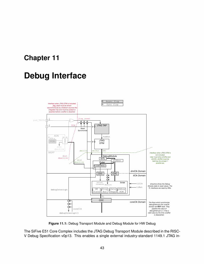
Figure 11.1: Debug Transport Module and Debug Module for HW Debug
The SiFive E51 Core Complex includes the JTAG Debug Transport Module described in the RISC-V Debug Specification v0p13. This enables a single external industry-standard 1149.1 JTAG in-
43

44 SiFive E51 Core Complex Series Manual v1p2
terface to test and debug the system. The JTAG interface can be directly connected off-chip in asingle-chip microcontroller, or can be an embedded JTAG controller for a RISC-V Core IP designedto be included in a larger SoC.
The Debug Transport Module and Debug Module are depicted in Figure 11.1.
On-chip JTAG connections must be driven (no pullups), with a normal two-state driver for TDOunder the expectation that on-chip mux logic will be used to select between alternate on-chipJTAG controllers’ TDO outputs. TDO logic changes on the falling edge of TCK.
11.1 JTAG TAPC State MachineThe JTAG controller includes the standard TAPC state machine shown in Figure 11.2.
Run-Test-Idle
Test-Logic-Reset
Select-DR-Scan
Capture-DR
Exit-1-DR
Exit-2-DR
Update-DR
Pause-DR 0
0Shift-DR
0
0
1
0
1
1
1
0
1
1
0
01
1 0
Select-IR-Scan
Capture-IR
Exit-1-IR
Exit-2-IR
Update-IR
Pause-IR 0
0Shift-IR
0
0
1
0
1
1
1
1 0
1 1
1
0
TRST=0
Figure 11.2: JTAG TAPC state machine. The state machine is clocked with TCK. All transitions are labelledwith the value on TMS, except for the arc showing asynchronous reset when TRST=0.
11.2 Resetting JTAG logicThe JTAG logic must be asynchrously reset by asserting jtag reset before coreReset is de-asserted.
Asserting jtag reset resets both the JTAG DTM and Debug Module test logic. Because parts ofthe debug logic require synchronous reset, the jtag reset signal is synchronized inside the E51Core Complex.
During operation the JTAG DTM logic may also be reset without jtag reset by issuing 5 TCK clockticks with TMS asserted. This action only resets the JTAG DTM, not the Debug Module.
11.2.1 JTAG ClockingThe JTAG logic always operates in its own clock domain clocked by TCK. The JTAG logic is fullystatic and has no minimum clock frequency. The maximum TCK frequency is part-specific.

Copyright c© 2016-2017, SiFive Inc. All rights reserved. 45
11.2.2 JTAG Standard InstructionsThe JTAG DTM implements the BYPASS and IDCODE instructions. The Manufacturer ID field ofIDCODE is provided by the RISC-V Core IP integrator, on the jtag mfr id input.
11.3 JTAG Debug CommandsThe JTAG DEBUG instruction gives access to the SiFive debug module by connecting the debugscan register inbetween TDI and TDO.
The debug scan register includes a 2-bit opcode field, a 7-bit debug module address field, anda 32-bit data field to allow various memory-mapped read/write operations to be specified with asingle scan of the debug scan register.
These are described in the RISC-V Debug Specification v0p13.
11.4 Using Debug OutputsThe Debug logic in SiFive Systems drives two output signals: ndreset and dmactive. Thesesignals can be used in integration. It is suggested that the indreset signal contribute to thesystem reset. It must be synchronized before it contributes back to the RISC-V Core IP’s overallreset signal. This signal must not contribute to the jtag reset signal. The dmactive signal maybe used to e.g. prevent clock or power gating of the Debug Module logic while debugging is inprogress.

46 SiFive E51 Core Complex Series Manual v1p2
Chapter 12
References
Visit the SiFive forums for support and answers to frequently asked questions: http://forums.
sifive.com.
[1] A. Waterman and K. Asanovic, Eds., The RISC-V Instruction Set Manual, Volume I:User-Level ISA, Version 2.2, May 2017. [Online]. Available: https://riscv.org/specifications/
[2] ——, The RISC-V Instruction Set Manual Volume II: Privileged Architecture Version 1.10, May2017. [Online]. Available: https://riscv.org/specifications/
47


