HAL Id: tel-00351281 https://tel.archives-ouvertes.fr/tel-00351281 Submitted on 8 Jan 2009 HAL is a multi-disciplinary open access archive for the deposit and dissemination of sci- entific research documents, whether they are pub- lished or not. The documents may come from teaching and research institutions in France or abroad, or from public or private research centers. L’archive ouverte pluridisciplinaire HAL, est destinée au dépôt et à la diffusion de documents scientifiques de niveau recherche, publiés ou non, émanant des établissements d’enseignement et de recherche français ou étrangers, des laboratoires publics ou privés. Signatures de l’injection optique et électrique de charges dans des monocristaux de rubrene Nripan Mathews To cite this version: Nripan Mathews. Signatures de l’injection optique et électrique de charges dans des monocristaux de rubrene. Matériaux. Université Pierre et Marie Curie - Paris VI, 2008. Français. <tel-00351281>
Transcript
HAL Id: tel-00351281https://tel.archives-ouvertes.fr/tel-00351281
Submitted on 8 Jan 2009
HAL is a multi-disciplinary open accessarchive for the deposit and dissemination of sci-entific research documents, whether they are pub-lished or not. The documents may come fromteaching and research institutions in France orabroad, or from public or private research centers.
L’archive ouverte pluridisciplinaire HAL, estdestinée au dépôt et à la diffusion de documentsscientifiques de niveau recherche, publiés ou non,émanant des établissements d’enseignement et derecherche français ou étrangers, des laboratoirespublics ou privés.
Signatures de l’injection optique et électrique de chargesdans des monocristaux de rubrene
Nripan Mathews
To cite this version:Nripan Mathews. Signatures de l’injection optique et électrique de charges dans des monocristaux derubrene. Matériaux. Université Pierre et Marie Curie - Paris VI, 2008. Français. <tel-00351281>
Pour obtenir le grade de DOCTEUR DE L’UNIVERSITE PARIS 6
Signatures of optically and electrically injected charges in rubrene single crystals
Soutenue le 19 septembre 2008
devant le jury composé de : Dr Denis FICHOU Directeur de thèse Pr Max MALACRIA Examinateur Dr Dominique VUILLAUME Rapporteur Dr Alberto MORPURGO Rapporteur Pr Subodh MHAISALKAR Examinateur Pr Freddy BOEY Examinateur
Thèse préparée au: CEA Saclay, LRC Nanostructures et Semi-Conducteurs Organiques
CNRS-CEA-UPMC
I
Abstract
Organic single crystals are of particular fundamental interest as tools in probing the
intrinsic electrical properties and the upper limit of performance for a given organic
semiconducting molecule devoid of disorder. Rubrene single crystals are of particular
interest in the field of organic electronics due to the high levels of charge carrier
mobilities measured in transistors constructed of the same. In this thesis, we explore
the properties of rubrene single crystal transistors.
The photocurrent properties of rubrene single crystals are measured in ‘air-gap’
transistors whose unique structure allows the measurement of photocarrier dynamics
without the influence of a dielectric that can act as a source for traps. This structure
has allowed us to identify phenomenon like persistent photoconductivity associated
with the creation of oxygen related traps on the rubrene surface. Transient studies of
the photocurrent reveal the presence of bimolecular recombination of the charge
carriers. In addition, we have also performed optical spectroscopy studies including
Raman spectra measurements which revealed the presence of endoperoxide related
signature on the surface of the crystal while also confirming the low levels of
intermolecular coupling present between the molecules.
We have also explored the extrinsic factors that determine the surface conductivity of
the rubrene crystal, particularly the presence of oxide related compounds on the
surface of the crystal using XPS and photoluminescence measurements. The impact of
photo-oxidation of the rubrene crystal on the surface conductivities were evaluated by
a novel experiment involving the gradual photo-oxidation of the rubrene surface using
a focussed laser. The creation of a deep acceptor state that can trap electrons indicates
that the electrical properties of the rubrene surface like high unipolar p-type
II
conductivity and photoconductivity may be modulated by the presence of these
oxygen induced states.
III
Acknowledgements
The past three years spent in pursuing a PhD has taught me many valuable lessons and
brought me in contact with many people who have been a pleasure to work with and who
have affected my life in many ways. It is my great pleasure to acknowledge them here.
First of all, I would like to thank Dr Denis Fichou for having supervised my thesis at
CEA-Saclay. Your perspective and knowledge of organic electronics, as well as your
advice on how to manage research is greatly appreciated. I will remember your advice
about always ‘putting things in the box’. I would also like to thank Prof Subodh
Mhaisalkar for having co-supervised me. Your enthusiasm, ideas and energy during the
past three years have been instrumental in ensuring the completion of this thesis. Your
flexibility and patience was very helpful in trying to balance work between Singapore
and France.
I also gratefully acknowledge the help and collaboration from Dr. Vitaly Podzorov and
Dr. Etienne Menard. I am very thankful for the discussions and suggestions regarding my
work. My gratitude also goes to Dr Tripathy and Mr Keke Zhang for help with the
measurements for Raman spectra and gas sensing respectively.
My PhD journey would have been a lot harder if it was not for the support, help and
sympathetic ears provided to me by my friends and colleagues in both France and
Singapore. My heartfelt as well as ‘stomach felt’ appreciation go to Ludovic, Camille,
Claudia, Odile, Alexandre, Giulia, Luc, Vadym, Vladymyr and Stephane. A special thank
you also goes to Alexander Marchenko for his help during my time in France. Spending
time in France has been a wonderful experience because of all you.
IV
I am also grateful to all my friends in Singapore. At the polymer electronics group in
Nanocluster, I would like to show gratitude to Wei Lin for being the sounding board for
many of my ideas and for help with the experimentation, as well as Willy, Anup, Zong
Bin, Tommy, Ju Nie, Phoebe, Vera and Victor. You all have been instrumental in
creating a good fun filled environment to work in and for keeping my spirits high when
things do not go well.
Last but definitely not the least; I would like to thank my family. I greatly acknowledge
my parents who have supported me through all the decisions I have made and whose
concern and love for me gives me hope and encouragement every day. Thank you my
brother and sister-in-law for your patience and love as well.
V
Dedicated to my parents
VI
Table of Contents
Page
Abstract I
Acknowledgements III
Table of Contents VI
List of Figures IX
List of Tables XV
1. General Introduction 1
1.1 Thesis overview 4
1.2 References 6
2. Electronic properties of molecular crystals 9
2.1 Organic semiconducting molecules 10
2.2 Intermolecular interaction 12
2.3 Charge transport characteristics of organic single crystals 16
2.3.1 Band like transport 16
2.3.2 Influence of traps 18
2.3.3 Polaron transport 21
2.4 References 26
3 Free-space dielectric field effect transistors 31
3.1 Single crystal growth 32
3.2 Organic single crystal transistors 34
VII
3.2.1 Elastomeric transistor stamps 36
3.3 Air-gap stamps 37
3.3.1 Fabrication of air-gap stamps 38
3.4 Working principle of field effect transistors 39
3.5 Contact effects in transistors 44
3.6 References 49
4 Photoconductivity in rubrene single crystals 53
4.1 Photoexcitation picture in organic molecular crystals 54
4.2 Excitons 55
4.2.1 Frenkel excitons 56
4.2.2 Wannier-Mott excitons 56
4.2.3 Charge-transfer excitons 57
4.3 Basic concepts of photoconductivity 59
4.4 Transient photoconductivity 61
4.4.1 Monomolecular recombination 62
4.4.2 Bimolecular recombination 63
4.5 Steady state photoconductivity measurements in rubrene transistors 64
4.6 Photocurrent transients measured under pulsed illumination 73
4.7 References 79
5 Optical Characterisation of rubrene crystals 82
5.1 Absorption and luminescence in Rubrene 83
5.1.1 Theory 83
5.1.2 Absorption spectra of rubrene solution and crystals 85
5.2 Photoluminescence Spectroscopy 88
5.2.1 Theory 88
VIII
5.2.2 Luminescence in conjugated systems 89
5.2.3 Luminescence in rubrene solutions and crystal 91
5.3 Raman spectroscopy 94
5.3.1 Theory 94
5.3.2 Experimental 96
5.3.3 Rubrene Single Crystal Raman spectra 98
5.3.4 Raman spectra for the different facets of the crystal 104
5.3.5 Temperature dependency 104
5.3.6 Electric field dependencies 106
5.4 References 109
6 Extrinsic effects on charge conducting properties of rubrene 112
6.1 Common extrinsic effects in organic devices 112
6.2 Oxidation of rubrene in solution 115
6.3 Photoluminescence measurements on rubrene crystal surface 117
6.4 X-ray Photoelectron Spectroscopy 118
6.5 In-situ photo-oxidation measurements 120
6.6 Source of conductivity modulation induced by oxygen effects 122
6.7 Influence of nitrogen dioxide on rubrene transistors 122
6.8 References 126
7 Conclusions and Perspectives 128
IX
List of Figures
Figure 1.1: Molecular structure of rubrene showing the tetracene backbone and the four
pendant phenyl rings in a twisted configuration ………………………………………....3
Figure 2.1: Chemical structure of some widely used semiconducting organic
polymers…………………………………………………………………………….........9
Figure 2.2: Chemical structure of some well known small molecule semiconductors…10
Figure 2.3: Creation of delocalized π electron system in a benzene molecule-the building
block of the acene group ……………………………………….....................................11
Figure 2.4: Energy levels of (single) ionic states of the acenes from benzene to pentacene
for the free molecule in the gas (g) state (left, solid lines), and for the crystal (c) (right,
double lines), defined by the electron-binding energy relative to the vacuum level. Ig and
Ic stand for ionization energies for gas phase and crystalline phase, Ag and Ac for electron
affinities for gas and solid phases, Pe and Ph for electron and hole polarization energies
respectively…………………………………………………………………………..…12
Figure 2.5: A top view of the ab- plane crystal structure of rubrene. The herringbone
configuration is apparent……………………………………………………………..…14
Figure 2.6: (Left) Molecular packing in the rubrene crystal. Blue arrow indicates the
direction of highest mobility (Right) Charge carrier mobility anisotropy on the surface of
rubrene crystal………………………………………………………………………… 15
X
Figure 2.7: Electron and hole mobilities in the a-direction of highly purified naphthalene
crystals for different field strengths…………………………………………………….17
Figure 2.8: Temperature dependent conductivity measurements on the rubrene transistor
showing the trap limited regime at low temperatures and intrinsic regime at higher
temperatures…………………………………………………………………………….20
Figure 2.9: Temperature dependence of the carrier mobility for six different gate
dielectrics. The temperature dependence evolves from metallic-like to insulator-like, as
the dielectric constant is increased……………………………………………………..24
Figure 3.1: Schematic of the PVT crystal growth……………………………………...32
Figure 3.2: Transistor fabrication by lamination of an organic crystal against the
transistor stamp. Initiating contact between the two surfaces results in a wetting front that
progresses across the semiconductor-stamp interface until the entire crystal is in intimate
contact with the stamp………………………………………………………………….36
Figure 3.3: Schematic illustration of the construction of organic single crystal transistors
with free space gate dielectrics…………………………………………………………38
Figure 3.4:a) Idealized energy level diagram of an organic TFT at VG = 0 and VD = 0. (b-
e) Demonstrate the principle of field effect transistor operation for the case of (b) electron
accumulation, (d) transport, (c) hole accumulation, and (e) transport…………………41
XI
Figure 3.5: Output characteristics of a rubrene air-gap transistor (L=300 µm, W=1000µm)
measured at 295K and 210K illustrating contact effects……………………………….44
Figure 3.6: Mobility dependence on temperature for saturation and linear regime
indicating the influence of the contacts. Activation energy extracted using simple
Arrhenius dependence shows Ea=0.059eV for saturation regime, 0.1eV for linear
regime…………………………………………………………………………………..47
Figure 4.1: Energy band diagrams of photoexcitations in organic semiconductors
according to semiconductor band model (left) and molecular exciton model (right)….54
Figure 4.2: Illustration of the charge delocalization in Wannier-Mott and Frenkel
excitons…………………………………………………………………………………57
Figure 4.3: Descriptions of photoexcitations in organic molecular crystals……………58
Figure 4.4: Simplest setup for measuring photoconductivity…………………………. 60
Figure 4.5: Illumination configuration during phototransistor measurements…………65
Figure 4.6: Output characteristics of a representative rubrene transistor in dark and under
poly(9,9-dioctylfluorene-co-bithiophene) (F8T2)7 and poly(2,5-bis(3-alkylthiophen-2-
yl)thieno[3,2-b]thiophenes) (PTTT) 8fall into this category of compounds.
S
S S
S
C6H13
C6H13
C6H13
C6H13
n
S
S S
S
C12H25
C12H25
n
C8H17H17C8
SS
n
n
S
C14H25
S
S
S
H25C14
P3HT PQT-12
F8T2 PTTT-14
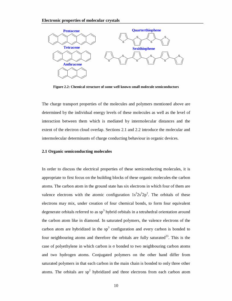
Figure 2.1: Chemical structure of some widely used semiconducting organic polymers
Small molecules on the other hand have low molecular weights and are normally
deposited by thermal evaporation. They normally consist of acenes like pentacene,
tetracene, anthracene9-17 as well as oligomers like quarterthiophene, sexithiophene18-22.
Electronic properties of molecular crystals
10
S
S S
S
S
S
S
S S
S
Pentacene
Tetracene
Anthracene
Quarterthiophene
Sexithiophene
Figure 2.2: Chemical structure of some well known small molecule semiconductors
The charge transport properties of the molecules and polymers mentioned above are
determined by the individual energy levels of these molecules as well as the level of
interaction between them which is mediated by intermolecular distances and the
extent of the electron cloud overlap. Sections 2.1 and 2.2 introduce the molecular and
intermolecular determinants of charge conducting behaviour in organic devices.
2.1 Organic semiconducting molecules
In order to discuss the electrical properties of these semiconducting molecules, it is
appropriate to first focus on the building blocks of these organic molecules-the carbon
atoms. The carbon atom in the ground state has six electrons in which four of them are
valence electrons with the atomic configuration 1s22s22p2. The orbitals of these
electrons may mix, under creation of four chemical bonds, to form four equivalent
degenerate orbitals referred to as sp3 hybrid orbitals in a tetrahedral orientation around
the carbon atom like in diamond. In saturated polymers, the valence electrons of the
carbon atom are hybridized in the sp3 configuration and every carbon is bonded to
four neighbouring atoms and therefore the orbitals are fully saturated23. This is the
case of polyethylene in which carbon is σ bonded to two neighbouring carbon atoms
and two hydrogen atoms. Conjugated polymers on the other hand differ from
saturated polymers in that each carbon in the main chain is bonded to only three other
atoms. The orbitals are sp2 hybridized and three electrons from each carbon atom
Electronic properties of molecular crystals
11
reside in the three σ-bonding orbitals, forming covalent bonds with the other atoms.
The remaining unpaired electron remains in the delocalized 2pz orbital with its charge
density lobes perpendicular to the plane defined by the σ-bonds. These pz orbitals can
then overlap to form delocalized π bands which make the conjugated polymers metals
or semiconductors depending on whether the bands are filled or partially filled.
The π-electrons are delocalized over several carbon atoms in the polymeric chain to
form π-bands. The presence of an energy gap between the filled and empty bands
imparts a semiconducting nature to the polymer instead of a metallic one. The
delocalized π-electrons are primarily responsible for the electrical and optical
properties in these systems. Equivalently the π bonding and antibonding orbitals can
be visualized to form a continuum of energy states rather than a discreet one. The
resultant continuum of antibonding and bonding orbitals are referred to as lowest
unoccupied molecular orbital (LUMO) and highest occupied molecular orbital
(HOMO) respectively. The HOMO and LUMO with an energy gap between them is
analogous to the valence and conduction bands in any inorganic semiconductor.
Figure 2.3: Creation of delocalized π electron system in a benzene molecule-the building block of the acene group
In the case of small molecule semiconductors like acenes with the benzene ring as the
basic unit, the π bonds become delocalized and form a π system that extends
throughout the system (Figure 2.3). The gap between occupied and unoccupied states
in this π system becomes lesser with increased delocalization in the system. Thus
Electronic properties of molecular crystals
12
pentacene with its 5 aromatic rings acts a semiconductor, while benzene remains an
electrical insulator (Figure 2.4). Charge carriers can easily move along a conjugated
molecule because of the presence of the delocalised molecular orbitals. For example,
in oligomers with well defined chain lengths, it has been shown that the primary gap
excitations are delocalized over the entire molecule and that the corresponding
excitons scale with the length of the molecule24. In contrast, the charge carriers move
with greater difficulty between different molecules due to the fact that conjugated
semiconductors in their thin film form are disordered materials with a low degree of
crystallinity.
Figure 2.4: Energy levels of (single) ionic states of the acenes from benzene to pentacene for the free molecule in the gas (g) state (left, solid lines), and for the crystal (c) (right, double lines), defined by the electron-binding energy relative to the vacuum level. Ig and Ic stand for ionization energies for gas phase and crystalline phase, Ag and Ac for electron affinities for gas and solid phases, Pe and Ph for electron and hole polarization energies respectively.
2.2 Intermolecular interaction
Efficient charge transport requires that the charges be able to move from molecule to
molecule and not be trapped or scattered. Thus charge carrier mobilities are
influenced by many factors including molecular packing, disorder and the presence of
impurities. In molecular crystals, the molecules are held together in a lattice by weak
forces. These forces (primarily van der Waals interaction) are much weaker than the
Electronic properties of molecular crystals
13
intramolecular covalent bonds such that the molecular properties are hardly affected
by the intermolecular interactions. The weakness of the intermolecular forces in
molecular crystals is expressed in the low mechanical strengths of these crystals as
well as their propensity to form polymorphs. For example in pentacene, four
polymorphs have been detected by Mattheus et al25-27, all of which are layered
herringbone structures. These polymorphs can have different charge transport
properties caused due to the difference in the bandwidths of the conduction and
valence bands.28
The van der Waals force comes from the interaction of a fluctuating dipole moment
on a molecule, induced by the electron motion within the molecule, with the induced
dipole moment on a neighbouring molecule. In aromatic and heterocyclic molecular
crystals, the weakly bound and therefore easily polarisable π electrons provide van der
Waals interactions. The van der Waals force of interaction favours face to face
orientation of planar molecules in the lattice in order to maximise the interaction
energy. This co facial structure is not commonly seen in most organic crystals due to
the contribution of quadrupole-quadrupole interactions in π conjugated systems29, 30.
Due to the delocalization of the π electrons above and below the plane of the molecule
and the net positive charge in the plane of the molecule, the molecule resembles two
dipoles oriented head to head. This results in a quadrupolar field around the molecule
that provides a considerable share of the total intermolecular interaction. The
repulsion induced by the quadrupolar interaction is strongest in a co facial
arrangement due to the repulsion induced by the closest approaching π electron clouds.
Thus the interplay between the van der Waals forces and quadrupolar interaction
results determines the final order. Desiraju et al.31 defined four possible packing types
for polynuclear aromatic hydrocarbons : herringbone structure (naphthalene,
anthracene, tetracene32, pentacene33 and rubrene34, 35 ), sandwich herringbone structure
(pyrene, perylene), γ structure (benzopyrene, coronene) and β structure (trybenzopy-
Electronic properties of molecular crystals
14
rene, tetrabenzoperylene). Important work by Anthony et al28, 36 has shown that the
different types of packing are possible by varying the nature, size and position of
substituent groups on the pentacene backbone. Similar variations have been illustrated
in chloro and bromo substituted tetracene12 derivatives where the stacking structure
which enhances the π orbital overlap between the molecules (as compared to the
herringbone motif) results in an enhanced charge carrier mobility.
Figure 2.5: A top view of the ab- plane crystal structure of rubrene. The herringbone configuration is apparent.
Locally, charge transport in conjugated materials is determined by the charge transfer
from one neighbouring molecule to another and is therefore very sensitive to
orientation of the molecules with respect to each other. The electronic coupling
between adjacent molecules, quantified by the transfer integral t, is modulated by the
molecular arrangement and directly associated with the electronic mobility 37-39. In the
framework of these calculations, the amplitude of the electronic coupling is
influenced by the intermolecular separation distance, the molecular overlap, the length
of the molecule, and, in the case of herringbone structures, the rotation of molecular
planes38, 40-43.Thus transfer integrals between the adjacent molecules in these crystals
vary significantly depending on the crystallographic direction39, 41, 44. One apparent
implication is that the charge carrier mobility within a molecular plane (ab plane in
Electronic properties of molecular crystals
15
rubrene) is much more efficient in comparison to charge carrier transport between
layers (c direction). This strong anisotropy of transport properties of organic crystals
has been well documented in the TOF experiments45. The conductivity anisotropy
within the ab-plane is anticipated to be less pronounced. However, prior to the
development of single-crystal OFETs, the anisotropy had never been observed in the
field-induced transport on the surface of organic semiconductors. Several types of
single-crystal OFETs based on rubrene demonstrate anisotropy of surface
conductivity 46-48 . In rubrene devices based on PDMS stamps, the mobility along the
crystallographic b axis exceeds the mobility along the a axis by a factor of ~ 3 (Figure
2.6). Similar anisotropies have been observed for rubrene transistors with parylene
gate dielectrics as well. A clear correlation between the mobility and molecular
packing has also been found recently in a family of tetrathiafulvalene derivatives49
and in air-gap transistors built on tetracene crystals50. Recently, non-destructive
probing techniques have been developed that allow the exploration of these
anisotropies at high angular resolution without having to move the fragile crystals
around.51
Figure 2.6: (Left) Molecular packing in the rubrene crystal. Blue arrow indicates the direction of highest mobility (Right) Charge carrier mobility anisotropy on the surface of rubrene crystal46
Electronic properties of molecular crystals
16
2.3 Charge transport characteristics of organic single crystals
Due to the weak van der Waals bonding between the individual organic molecules,
many electronic properties of these organic solids are determined by the property of
the molecule itself- specifically the energy gap between the highest occupied and
lowest occupied molecular orbitals (HOMO and LUMO). The transport mechanism is
usually understood with respect to the limiting cases of small polaron transport and
bandlike transport corresponding to the extreme localization or delocalization of the
charge carriers.
2.3.1 Band like transport
The classical work performed by N. Karl and coworkers on highly purified
naphthalene and perylene single crystals revealed the first proof of band transport in
organic molecular crystals52-54.Mobilities as high as 400 cm2/Vs were obtained at 10K
and 3kV/cm by the time-of –flight method (Figure 2.7) in extremely pure naphthalene
crystals. These TOF velocities could not be explained by charge hopping models.
Electronic properties of molecular crystals
17
Figure 2.7: Electron and hole mobilities in the a-direction of highly purified naphthalene crystals for different field strengths. Adapted from 53
In addition, the sub-linear velocity-field relation at high fields observed in these
samples could be explained by the Schottky model of acoustic deformation potential
scattering by hot charge carriers, a model which is based on band transport. Thus the
authors53 proposed that the charge carrier transport in pure and perfect low molecular
weight aromatic organic photoconductor crystals at low temperature can be described
by coherent transport in bands. Space charge limited current measurements on
ultrapure pentacene 55 as well as in tetracene 56 single crystals have shown intrinsic
band like transport. Picosecond transient photoconductivity measurements conducted
on a variety of organic crystals including rubrene support the band picture as well 57-59.
It is conceivable that in organic crystals where the molecules are in an ordered
arrangement, each molecular π system can interact with the π systems of the adjacent
Electronic properties of molecular crystals
18
molecules resulting in the formation of energy bands in the crystal. The crystal
valence bands originate from the overlapping HOMO’s of the individual molecules,
whereas the conduction band is formed by the overlapping of the LUMOs. The
organic semiconductors are normally characterized by wide bandgaps and small
bandwidths. The molecular crystal’s bandwidth is related to the orbital overlap
strength of the HOMOs and the LUMOs. Calculations have shown that the
bandwidths are in the range of 0.1 -0.5 eV 60-62. This compares unfavourably with the
values in inorganic semiconductors like silicon (10 eV) and could explain the huge
difference in the mobilities.
2.3.2 Influence of traps
Since organic crystals possess a better crystalline order and reduced concentration of
defects, they are expected to have a very low concentration of electrical traps. The
reduced number of defects still creates localized electrical states in the HOMO-
LUMO gap. The impact of these traps on the electrical transport properties depends
on their location in the energy gap. In the case of p-type carriers, if the traps exist near
the edge of HOMO, separated by energy of a few kBT, they act as shallow traps. If the
energy of the localized state is separated from the mobility edge by more than a few
kBT, they are characterized as deep traps. Once a charge is trapped in a deep state, it
cannot be released by thermal energy alone. For the pristine surface of rubrene single
crystals at room temperature, for instance, the density of deep traps can be as low as
1010 cm–2.Shallow traps on the other hand are characterized by a finite trapping time.
After being trapped for a characteristic time τtr, a polaron can be thermally activated
and released to the band. The effect of shallow traps on charge transport is normally
described in terms of the multiple trap and release (MTR)63, 64 model. According to
this model, not all the charges induced in the transistor on application of a voltage VG
above the threshold voltage Vth contributes to the current. A fraction of the mobile
charge can be momentarily trapped by shallow traps-the fraction being determined by
Electronic properties of molecular crystals
19
the number of traps and the temperature (which determines the τtr). This idea can be
represented in two ways- either by assuming that all the carriers induced above the
threshold flow, but with a lower effective mobility than the intrinsic mobility or by
assuming that the number of carriers moving at any time is limited, but they travel at
the intrinsic trap free mobility. The first approach can be described by:
)()(
)()(0 TT
TT
treff
ττ
τµµ
+=
Here τtr(T) is the average trapping time on shallow traps while τ(T) is the average time
that a polaron spends diffusively travelling between the consecutive trapping events.
Thus the intrinsic mobility is only realised when the τ is much more than τtr which
happens when there is a low concentration of defects or when the temperature is high
enough to ensure rapid detrapping. This regime allows the exploration of the intrinsic
properties of the crystal surface like mobility anisotropy.
Electronic properties of molecular crystals
20
Figure 2.8: Temperature dependent conductivity measurements on the rubrene transistor showing the trap limited regime at low temperatures and intrinsic regime at higher temperatures
Figure 2.8 reveals the two regimes at play in the temperature dependent characteristics
of rubrene single crystal transistors. At higher temperatures (above 150K), the
intrinsic properties like the pronounced anisotropy difference for conductivity along
the b-axis and the a-axis. As the temperature is lowered, the charges localized in the
shallow traps are released after a much longer timescale. This is indicated by the rapid
fall in mobility values below 150K where the traps dominate. This transition
temperature would be strongly dependent on the concentration of the traps with a
higher concentration shifting this threshold to a higher temperature. The classical
work performed by N.Karl and co-workers on ultrapure crystals of naphthalene and
perylene revealed similar results with an increase in the mobility (up to 400 cm2/Vs)
Electronic properties of molecular crystals
21
with the lowering of temperature (intrinsic regime) until the shallow traps become
active and result in a reduction of the effective mobility.47, 53
The high-quality TOF data of Karl et al implies that coherent transport characterizes
the intrinsic charge transport in ultra-pure organic single crystals. However the
calculation of the charge carrier’s mean free path from experimental evidence
indicates that they are smaller than the intermolecular distance62. This of course
violates the assumption of charge delocalization necessary for the band model. In
narrow-band molecular solids, polarization effects favor localization of charge
carriers and narrow the bandwidth even further. This results in self-trapped electronic
states called polarons which differ in their behavior from nearly free electrons
(necessary for band-type behavior) and strongly localized electrons (which can lead to
hopping behavior). The next section discusses polaron formation and transport
2.3.3 Polaron transport
Polarons are quasiparticles composed of a charge carrier accompanying its
polarization field. The polarization field causes a distortion in the local lattice. As the
charge moves through the crystal, the electron carries the lattice distortion with it. The
resulting lattice polarization acts as a potential well that hinders the movements of the
charge, thus decreasing the mobility. In an organic molecular crystal, the polarization
associated with the charge include the polarization of the electronic orbitals on
molecules surrounding the excess charge which is caused due to the interaction of the
charge with the induced dipole moments and quadrupole moments of the surrounding
molecules.
The term of polaron owes its origin to that it was considered for the case of polar
crystals, where interactions between electrons and optical polarizations are
Electronic properties of molecular crystals
22
particularly strong, so that an excess carrier creates a local distortion of the lattice in
which it is self-trapped. The indications for polaron-formation in organic molecular
crystals can be seen in photo-emission experiments.62 Photoemission data from single
crystals generally show lines that are broadened and shifted in energy relative to the
corresponding gas phase spectral lines. The broadening is suggested to originate from
fluctuations in the intermolecular electronic polarization while the spectral line shift
can be explained by the increased binding energy of a charge due to polarizations in
the local crystal environment. Pioneering theoretical work in this area was done by
Holstein65, who introduced the concept of small-polaron bands for a local (on-site)
electron –phonon coupling. A small polaron is one whose linear dimensions are of the
order of one lattice spacing. The main prediction of his theory is that the mobilities
initially decrease with rising temperature T due to bandwidth narrowing but increase
again for higher T due to phonon-assisted hopping.
Interestingly electron mobility values of naphthalene single crystals below 100K
follows a power law (proportional to T-1.5) consistent with the band model. However,
between 100K and 300K the electron mobility along the crystallographic c direction
remains constant 45. This constant region has been described as the superposition of
two independent carrier mechanisms. According to Silinsh et al66 the first mechanism
is described using the concept of an adiabatic, nearly small molecular polaron (MP),in
which the carriers are treated as heavy polaron-type quasiparticles, which are formed
as a result of the interaction of the carriers with intramolecular vibrations of the local
lattice environment, and move coherently via tunneling. The second mechanism
involves a small lattice polaron (LP), which moves by thermally activated hopping
and thus exhibits a typical exponential dependence of mobility on temperature. This
polaronic hopping-type temperature dependence has also been measured for the
electron mobility in pyrene and for the hole mobility in perylene45. Kenkre et al67
were also able to fit the measured electron mobilities reasonably well to Holstein’s
model assuming directionally dependent local-coupling constants.
Electronic properties of molecular crystals
23
Despite the success of such fitting procedures, there was a need for a first-principles
description of charge-carrier mobilities in organic crystals that could explain the
different behavior of electrons and holes, the microscopic origin of the
crystallographic anisotropy in the temperature dependence and the influence of
nonlocal (Peierls-type) couplings. This has been compensated by the proposal of a
Holstein-Peierls model by Hannewald et al68, 69 which is based on Holstein’s original
concept of small-polaron bands but generalized with respect to the inclusion of
nonlocal electron-phonon coupling. Using this model and microscopic parameters
derived from ab-initio calculations, the authors were able to reproduce the
experimental data in naphthalene69. The model, however, only accounts for the
intermolecular optical modes and neglects the contribution from intra-molecular
vibrations and the coupling to acoustic modes that play a significant role in charge
transport.70
The polaron theories described above are mostly applicable to charge conduction in
the bulk of the crystal for a low density of charge carriers (as is the case in TOF
experiments). On the surface of rubrene single crystal transistors where the density of
charge carriers is much higher due to its proximity to a polar dielectric, conduction
has been proposed to occur through the motion of Fröhlich polarons71 In common
inorganic semiconductors, the effective strength of the interactions that create
Fröhlich polarons are weak due to both the low ionic polarizabilities and the low band
masses of these materials. This is not the case in organic transistors where the band
masses are high due to the weak van der Waals bonding while using gate dielectrics
with increasing ionic polarizabilities permits the strength of interaction to be tuned
from weak to the strong coupling regimes.
Electronic properties of molecular crystals
24
Figure 2.9: Temperature dependence of the carrier mobility for six different gate dielectrics. The temperature dependence evolves from metallic-like to insulator-like, as the dielectric constant is increased.
The gate modulated electrostatic ‘doping’ of charge carriers in organic single crystal
transistors allows the observation and study of new phenomena. For example, the use
of highly polarizable Ta2O5 gate dielectrics allows a high carrier density regime (0.1
carrier per molecule) which enables observation of coulombic repulsion in the
Fröhlich polarons and drain current saturation in transistors.72
Recently, Troisi 73et al have proposed in a recent computational paper that, at room
temperature, the transfer integral between close molecules is strongly modulated by
thermal motions. Since the amplitude of this modulation is of the same order of
magnitude as the average transfer integral, the translational symmetry of the
electronic Hamiltonian is completely lost and the overall electronic structure of the
crystal resembles that of an amorphous material. The sensitivity of the transfer
integral to small nuclear displacements (discussed previously in this chapter) was
recognized by these authors as the crucial difference between transport mechanisms in
Electronic properties of molecular crystals
25
organic and inorganic semiconductors. A minimalist model Hamiltonian37 that
neglects the effect of reorganization energy and considers only the fluctuation of the
transfer integral has been used to explain the temperature dependence of the charge
mobility of organic semiconductors and has been applied to predict the absolute
charge mobility of rubrene.74
In conclusion, this chapter has discussed the basic theory of charge transport in
organic crystals including the origin of semiconducting behaviour in organic
molecules. The intermolecular interactions that shape the order and arrangement of
organic molecules in lattices have been described. The position and orientation of the
molecules modulate the intermolecular transfer integral which determines the charge
transfer properties of these molecules. The band model which is commonly used to
discuss the charge transport in single crystals was also introduced here along with the
characteristics of polaron transport in these materials. The widespread interest in
unraveling the underlying factors determining the charge transport is spurring the
development of new theories which consider local and non-local interactions between
the charge carrier and its environment.
Electronic properties of molecular crystals
26
2.4 References
1. A. Assadi, C. Svensson, M. Willander and O. Ingana?s, Applied Physics
Letters, 1988, 53, 195-197.
2. Z. Bao, A. Dodabalapur and A. J. Lovinger, Applied Physics Letters, 1996, 69,
4108-4110.
3. R. J. Kline, M. D. McGehee, E. N. Kadnikova, J. Liu, J. M. J. Fre?chet and M.
F. Toney, Macromolecules, 2005, 38, 3312-3319.
4. J. Paloheimo, H. Stubb, P. Yli-Lahti and P. Kuivalainen, Synthetic Metals,
1991, 41, 563-566.
5. A. Tsumura, H. Koezuka and T. Ando, Applied Physics Letters, 1986, 49,
1210-1212.
6. B. S. Ong, Y. Wu, P. Liu and S. Gardner, Journal of the American Chemical
Society, 2004, 126, 3378-3379.
7. E. Lim, Y. M. I. Kim, J. I. K. Lee, B. J. Jung, N. S. Cho, J. Lee, D. O. Lee-Mi
and H. K. Shim, Journal of Polymer Science, Part A: Polymer Chemistry,
2006, 44, 4709-4721.
8. H. Sirringhaus, R. J. Wilson, R. H. Friend, M. Inbasekaran, W. Wu, E. P. Woo,
M. Grell and D. D. C. Bradley, Applied Physics Letters, 2000, 77, 406-408.
9. J. G. Laquindanum, H. E. Katz, A. J. Lovinger and A. Dodabalapur, Chemistry
of Materials, 1996, 8, 2542-2544.
10. Y. Y. Lin, D. J. Gundlach and T. N. Jackson, Annual Device Research
Conference Digest, 1996.
11. Y. Y. Lin, D. J. Gundlach, S. F. Nelson and T. N. Jackson, IEEE Electron
Device Letters, 1997, 18, 606-608.
12. H. Moon, R. Zeis, E. J. Borkent, C. Besnard, A. J. Lovinger, T. Siegrist, C.
Kloc and Z. Bao, Journal of the American Chemical Society, 2004, 126,
15322-15323.
13. M. L. Tang, A. D. Reichardt, N. Miyaki, R. M. Stoltenberg and Z. Bao,
Journal of the American Chemical Society, 2008, 130, 6064-6065.
14. C. D. Dimitrakopoulos, A. R. Brown and A. Pomp, Journal of Applied Physics,
1996, 80, 2501-2508.
15. C. D. Dimitrakopoulos, S. Purushothaman, J. Kymissis, A. Callegari and J. M.
Shaw, Science, 1999, 283, 822-824.
Electronic properties of molecular crystals
27
16. H. Klauk, M. Halik, U. Zschieschang, G. Schmid, W. Radlik and W. Weber,
Journal of Applied Physics, 2002, 92, 5259.
17. S. F. Nelson, Y. Y. Lin, D. J. Gundlach and T. N. Jackson, Applied Physics
Letters, 1998, 72, 1854-1856.
18. F. Garnier, G. Horowitz and D. Fichou, Synthetic Metals, 1989, 28, 705-714.
19. F. Garnier, G. Horowitz, D. Fichou and A. Yassar, Synthetic Metals, 1996, 81,
163-171.
20. F. Garnier, G. Horowitz, X. Peng and D. Fichou, Advanced Materials, 1990, 2,
592-594.
21. F. Garnier, G. Horowitz, X. Z. Peng and D. Fichou, Synthetic Metals, 1991, 45,
163-171.
22. G. Horowitz, D. Fichou, X. Peng, Z. Xu and F. Garnier, Solid State
Communications, 1989, 72, 381-384.
23. J. March, Advanced Organic Chemistry, John Wiley & Sons, New York, 1985.
24. M. Knupfer, J. Fink, E. Zojer, G. Leising and D. Fichou, Chemical Physics
Letters, 2000, 318, 585-589.
25. C. C. Mattheus, A. B. Dros, J. Baas, A. Meetsma, J. L. De Boer and T. T. M.
48. R. Zeis, C. Besnard, T. Siegrist, C. Schlockermann, X. Chi and C. Kloc,
Chemistry of Materials, 2006, 18, 244.
Electronic properties of molecular crystals
29
49. M. Mas-Torrent, P. Hadley, S. T. Bromley, X. Ribas, J. Tarre?s, M. Mas, E.
Molins, J. Veciana and C. Rovira, Journal of the American Chemical Society,
2004, 126, 8546.
50. X. Yu, V. Kalihari, C. D. Frisbie, N. K. Oh and J. A. Rogers, Applied Physics
Letters, 2007, 90, 162106.
51. M. M. Ling, C. Reese, A. L. Briseno and Z. Bao, Synthetic Metals, 2007, 157,
257.
52. N. Karl, J. Marktanner, R. Stehle and W. Warta, Synthetic Metals, 1991, 42,
2473-2481.
53. W. Warta, R. Stehle and N. Karl, Applied Physics A Solids and Surfaces, 1985,
36, 163.
54. W. Warta and N. Karl, Physical Review B, 1985, 32, 1172-1182.
55. O. D. Jurchescu, J. Baas and T. T. M. Palstra, Applied Physics Letters, 2004,
84, 3061-3063.
56. R. W. I. de Boer, M. Jochemsen, T. M. Klapwijk, A. F. Morpurgo, J. Niemax,
A. K. Tripathi and J. Pflaum, Journal of Applied Physics, 2004, 95, 1196-1202.
57. V. K. Thorsmolle, R. D. Averitt, X. Chi, D. J. Hilton, D. L. Smith, A. P.
Ramirez and A. J. Taylor, Applied Physics Letters, 2004, 84, 891-893.
58. O. Ostroverkhova, D. G. Cooke, S. Shcherbyna, R. F. Egerton, F. A. Hegmann,
R. R. Tykwinski and J. E. Anthony, Physical Review B - Condensed Matter
and Materials Physics, 2005, 71, 1-6.
59. O. Ostroverkhova, D. G. Cooke, F. A. Hegmann, J. E. Anthony, V. Podzorov,
M. E. Gershenson, O. D. Jurchescu and T. T. M. Palstra, Applied Physics
Letters, 2006, 88, 162101-162103.
60. G. Brocks, J. van den Brink and A. F. Morpurgo, Physical Review Letters,
2004, 93, 146405.
61. R. Silbey, J. Jortner, S. A. Rice and J. M. T. Vala, The Journal of Chemical
Physics, 1965, 42, 733-737.
62. M. Pope and C. E. Swenberg, Electronic Processes in Organic Crystals and
Polymers, 1999.
63. G. Horowitz, Journal of Materials Research, 2004, 19, 1946.
64. G. Horowitz and M. E. Hajlaoui, Advanced Materials, 2000, 12, 1046.
65. T. Holstein, Annals of Physics, 1959, 8, 343.
Electronic properties of molecular crystals
30
66. E. A. Silinsh, A. Klimkans, S. Larsson and V. Cápek, Chemical Physics, 1995,
198, 311-331.
67. V. M. Kenkre, J. D. Andersen, D. H. Dunlap and C. B. Duke, Physical Review
Letters, 1989, 62, 1165-1168.
68. K. Hannewald, V. M. Stojanovic, J. M. T. Schellekens, P. A. Bobbert, G.
Kresse and J. Hafner, Physical Review B - Condensed Matter and Materials
Physics, 2004, 69, 752111-752117.
69. K. Hannewald and P. A. Bobbert, Applied Physics Letters, 2004, 85, 1535-
1537.
70. V. Coropceanu, J. Cornil, D. A. da Silva Filho, Y. Olivier, R. Silbey and J. L.
Brédas, Chemical Reviews, 2007, 107, 926-952.
71. I. N. Hulea, S. Fratini, H. Xie, C. L. Mulder, N. N. Iossad, G. Rastelli, S.
Ciuchi and A. F. Morpurgo, Nature Materials, 2006, 5, 982-986.
72. S. Fratini, H. Xie, I. N. Hulea, S. Ciuchi and A. F. Morpurgo, New Journal of
Physics, 2008, 10, 033031.
73. A. Troisi and G. Orlandi, Journal of Physical Chemistry A, 2006, 110, 4065-
4070.
74. A. Troisi, Advanced Materials, 2007, 19, 2000-2004.
Free-space dielectric field effect transistors
31
Chapter 3
Free-space dielectric field effect transistors
This chapter introduces the various fabrication techniques used in the construction of
organic single crystal transistors with a strong emphasis on free-space dielectric field
effect transistors. This was the configuration employed throughout the construction
and testing of rubrene single crystal transistors described in this thesis. General
characteristics of organic single crystal field effect transistors are described as well as
the influence of contacts on electrical characteristics extracted from the transistors.
Molecular crystals are of importance in the field of organic electronics due to the
opportunity that they allow for the exploration of fundamental properties without the
influence of disorder. Molecular crystals due to their rigid order and tendency to form
two dimensional crystallites are normally very fragile and difficult to handle. The
purity of the crystals makes it very sensitive to defects and contamination introduced
while fabricating devices. Traditionally, anthracene has been studied as a model
organic semiconductor and photoconductor with initial work on anthracene crystals
going as far back as 1906 1. The development of efficient purification methods2, 3
allowed the exploration of fundamental properties of anthracene such as its intrinsic
energy levels and its charge carrier transport properties4, 5. Since the explorations of
the properties of these molecules are possible only in high quality crystals, it is
relevant to begin the chapter with a brief discussion on the techniques used to prepare
the crystals.
Free-space dielectric field effect transistors
32
3.1 Single crystal growth
The most common way of growing organic crystals is in horizontal reactors in the
vapor phase in a stream of transport gas. In this Physical Vapor Transport (PVT)
method, the starting material is placed on the hottest region of the reactor and the
crystal is grown on the colder parts of the reactor. Heavy impurities (with a vapor
pressure lower than that of the pure organic compound) remain at the position of the
source material. Light impurities (with a vapor pressure higher than that of the pure
organic compound) condense at a lower temperature, i.e. at a different position from
where the crystals grow. Therefore, the crystal growth process also results in the
purification of the material. The characteristics of the crystal depends on the carrier
transport gas used (Argon is best for tetracene while hydrogen is best for rubrene)
although the mechanism is not clear. Good crystal growth involves very careful tuning
of parameters and precautions to prevent the creation of photoinduced oxidation
defects. Details of the physical vapour transport process have been described
exhaustively by a series of papers by Laudise and Kloc6, 7.
Figure 3.1: Schematic of the PVT crystal growth apparatus8
Free-space dielectric field effect transistors
33
Starting material is loaded into the source zone and maintained at a temperature Tsource,
where sublimation takes place, and molecules are carried by the gas stream into the
region of lower temperature. For a given concentration of evaporated molecules,
defined by the temperature Tsource, there is a point located downstream at a lower
temperature, growth, where crystallization occurs. At this point, the crystallization
rate (proportional to the density of molecular vapor) becomes slightly greater than the
rate of sublimation from crystal facets kept at temperature Tcrys. Although both
crystallization and sublimation occur at a facet simultaneously, the growth is favoured
and free-standing crystals grow. In the region to the left of the growth zone,
sublimation prevails and no growth occurs; in the region to the right (downstream),
the density of molecular vapor decreases and crystallization also does not occur. In
this region, only smaller molecular weight impurities condense. If the temperature of
the starting material is kept very close to the sublimation point, the heavier molecular
impurities do not sublime and remain in the source zone. Thus crystal growth by PVT
results in purification at the same time.
The crystals which are obtained after the PVT process (conducted over several tens of
hours) are normally in the form of platelets or needles. The crystal shape is controlled
by the anisotropy of intermolecular interactions: For many materials, the largest
crystal dimension corresponds to the direction of the strongest interactions and,
presumably, the strongest overlap of π-orbitals of adjacent molecules. For this reason,
the direction of the fastest growth of elongated rubrene crystals (b axis) coincides with
the direction of the highest mobility of field-induced carriers. In platelet-like crystals,
the largest natural facet typically corresponds to the a–b plane.
In some molecular crystals (eg. Anthracene), impurities have been shown to strongly
influence the electrical as well as the optical properties. This is similar to the case of
inorganic semiconductors like silicon where the impurity levels are kept below the
ppm range. Tetracene in ppm traces form shallow electron and hole traps at room
Free-space dielectric field effect transistors
34
temperature in anthracene single crystals. Introduction of an impurity with a smaller
ionization energy and/or larger electron affinity than the host molecules will form trap
levels in the energy gaps between the transport levels. Additional effects can also be
caused due to the excess strain induced by the inclusion of the impurity in the matrix.
This highlights the importance of starting the growth with pure organic powder. This
especially becomes important in the case of higher melting point hydrocarbons where
purification methods like zone-melting are not feasible 2. The rubrene crystals used in
this thesis have been prepared by Dr. Vitaly Podzorov at the Rutgers University using
hydrogen as a carrier gas. As the crystal growth process also results in the chemical
purification of the material, several re-growth cycles may be required for improving
the field-effect mobility, with the grown crystals used as the starting materials for the
subsequent regrowth.
3.2 Organic single crystal transistors
Broadly, single crystal transistors can be classified in two categories- top contact and
bottom contact. The top-contact SCFET configuration involves the fabrication of a
transistor structure directly on top of the organic single crystal and is at most times a
top-gate structure with the semiconductor crystal acting as the substrate. This
architecture requires that source and drain electrodes and dielectric are deposited onto
the surface of the single crystal. This is a very critical step in the fabrication of the
transistor. The commonly used methods include the application of conducting paste
and Ag epoxy 9, 10or direct shadow mask deposition11 onto the crystal surface. While
each of these methods is relatively straightforward and has been employed
successfully, both have been implicated in the formation of defects at the critical
semiconductor/electrode interface. During the application of the silver paste, the
solvents in the mixture will attack the surface of the organic crystal. Another
disadvantage of the manual application of electrodes is the difficulty in preparing
small and well shaped contacts. The direct deposition of electrodes on top of the
Free-space dielectric field effect transistors
35
crystal also results in damage due to the kinetic energy of the hot gold atoms arriving
from the source.
In addition, the manual application of electrodes and the limitation of shadow-mask
feature sizes necessitate large crystals and limits device density. Another critical step
is the deposition of a dielectric layer on top of the crystal which has proven even more
problematic. Attempts at sputtering Al2O3 and other dielectrics on the crystal resulted
in a very high density of traps and a prohibitively high field-effect threshold12. This
problem has been addressed with the introduction of a conformal evaporated parylene
dielectric film 11. With a very simple homemade reactor, an inert, pinhole-free,
conformal film can be controllably deposited onto the crystal surface without
apparently damaging it. A gate electrode deposited on this film completes the top-
contact, top-gate structure. Introduced by Podzorov et al., the technique has resulted
in high mobility being recorded in a variety of organic crystals and has been
instrumental in the investigation of intrinsic properties of the rubrene single crystal 13-
17.
The bottom-contact SCFETs take advantage of photolithography to pattern source and
drain electrodes as well as the dielectric on a substrate containing a gate electrode on
to which the crystal is placed or grown. The use of photolithography allows for the
patterning of features at length scales and densities impossible with top-contact
geometries. The ‘electrostatic bonding’ technique, in which a thin single crystal
adheres to the dielectric surface by simply being brought into contact, has been
performed on thermally grown SiO2 substrates 18-23 as well as other high k-dielectrics
deposited through sputtering.
Free-space dielectric field effect transistors
36
3.2.1 Elastomeric transistor stamps
The elastomeric technique developed by E. Menard et al also involved the
prefabrication of source/drain/ gate electrodes on a flexible elastomeric substrate. The
elastomeric technique, however, compares favorably with the Si-based technique in
two important aspects. Firstly, in contrast to Si-based substrates that require very thin
(~1 µm) and bendable crystals (which are prone to strain-induced defects), the
elastomeric stamps are compatible with much thicker (up to a few mm) and rigid
crystals: the flexible elastomeric surface and the ductile Au contacts adjust easily to
the crystal shape. Secondly, the elastomeric stamp technique is non-destructive and
reversible: the contact between the stamp and organic crystals can be re-established
many times without affecting the transistor characteristics. This experimental
capability was used to explore the dependence of the field effect mobility on the
orientation of the transistor channel relative to the crystallographic axes, and observed
for the first time a strong anisotropy of the field-effect mobility within the a-b plane of
single crystals of rubrene8, 24 (Chapter 2, Figure 2.6).
Figure 3.2: Transistor fabrication by lamination of an organic crystal against the transistor stamp. Initiating contact between the two surfaces results in a wetting front that progresses across the semiconductor-stamp interface until the entire crystal is in intimate contact with the stamp24
Free-space dielectric field effect transistors
37
3.3 Air-gap stamps
As mentioned previously, organic field effect transistors (OFETs) that facilitate
studies on the electrical characteristics of organic semiconductors are complex
structures whose properties depend on interactions between the semiconductor, gate
dielectric and electrodes. Carrier trapping, charge doping, molecular reorientation,
dipole formation and a range of possible chemical interactions are among the many
phenomena that can occur at the semiconductor/dielectric interface to degrade device
performance. 10, 11, 25-27.
E. Menard et al28 proposed an unusual device design that avoids these effects entirely
by replacing the standard solid dielectric layer with a thin free space gap that can be
filled with air, nitrogen, other gases or even vacuum. When combined with high-
quality organic crystals, this design reveals the ultimate in OFET performance,
determined solely by the intrinsic (not limited by disorder) polaronic transport on the
pristine surface of the crystals. Unlike the effects associated with electrical contacts,
which can be subtracted from the device response by four point probing or channel
length scaling analysis, it is difficult or impossible to predict or account for
interactions between a semiconductor and a conventional material dielectric23, 29. The
free space dielectric simply eliminates these effects by eliminating the dielectric
insulating material. It is uniquely well suited to the study of organic semiconductors,
which do not possess the types of dangling bonds or surface states that are present in
many inorganic materials. The advantages of this technique were demonstrated in the
construction of TCNQ single crystal transistors with high intrinsic carrier mobilities
of 1.6 cm2/Vs.28 It must be noted that transistors which were constructed using the
elastomeric stamp technique as well as with parylene as the dielectric showed much
lower mobilities.
Free-space dielectric field effect transistors
38
3.3.1 Fabrication of air-gap stamps
Figure 3.3: Schematic illustration of the construction of organic single crystal transistors with free space gate dielectrics.
Figure 3.3 schematically illustrates the steps for building these devices. The stamp is
fabricated by casting a pre-polymer of poly (dimethylsiloxane) (PDMS; Sylgard 184,
Dow Corning Corp.) against a pattern of photoresist (SU8) on a silicon wafer defines
an elastomeric element with relief features in the geometry of the resist. The PDMS
can also be casted on top of a master with relief features. The casted feature is left in
low vacuum to degas the mixture of PDMS and curing agent. After heating, the
PDMS hardens and can be carefully removed from the pattern. Coating this element
with a collimated flux of metal generates electrically isolated electrodes on the raised
and recessed regions. This single processing step defines source and drain (raised
regions) electrodes together with a self-aligned gate (recessed region) electrode. The
size of the electrodes and their separation are limited only by the resolution of soft
lithographic casting and curing procedures: dimensions as small as a few tens of
nanometers are possible30.
Free-space dielectric field effect transistors
39
Gently placing a single crystal sample on the surface of such an element leads to soft,
van der Waals contacts to the source/drain electrodes. The crystal itself forms a free
standing bridge that spans the gap between these electrodes. The thin space between
the bottom surface of the crystal and the gate electrode plays the role of the gate
dielectric. This space can be filled with any gas (e.g. air) or by vacuum, depending on
the experimental conditions. The standard spacing between the crystal and gate
electrodes of the stamps utilized in this thesis is 2 microns. The electrical breakdown
fields for air gaps which are much narrower than the mean free path of air molecule
can be exceptionally high due to the suppression of the avalanche phenomena that
generate discharges.31
3.4 Working principle of field effect transistors
The basic idea of a field effect transistor is to modulate the current that flows between
two ohmic contacts (source and drain electrodes) by applying a voltage to a third
contact (the gate electrode). The semiconductor film and the gate electrode are
capacitively coupled such that the application of a bias on the gate induces charge in
the semiconductor film. The inorganic Metal Insulator Field Effect Transistor
(MISFETs) normally operate in the inversion mode where the electric field applied at
the gate electrode is enough to induce minority carriers at the semiconductor-
dielectric interface. In the case of organic materials with the low density of charge
carriers, the preferred regime of operation is in the accumulation mode.
For a transistor based on a p-type semiconductor, the accumulation regime is induced
on the application of a sufficiently high negative gate voltage. The application of a
negative bias causes the HOMO and LUMO levels to shift up such that the HOMO
becomes resonant with the Fermi energy level of the contact. This allows the
Free-space dielectric field effect transistors
40
injection of holes from the contacts (or spilling of electrons from the semiconductor to
the contacts). The injected holes can then move under the application of an applied
drain electric field. In the case of an n-type transistor, the application of a positive
gate voltage results in the HOMO and LUMO levels shifting down so that the LUMO
levels align with the Fermi level of the electrode, allowing injection of electrons into
the semiconductor. In the following section, the general electrical features of a p-type
channel FET will be described.
Figure 3.4 shows the biasing conditions of the p-type transistors. Being a three
terminal device, the gate voltage modulates the current flowing between the source
and drain. In a p-type device, the threshold voltage Vth is normally negative. Thus for
the transistor to work, a more negative voltage VG than the threshold voltage should
be applied. By convention, the source electrode acts as the source of the carrier
flowing in the transistor. During the normal testing of a p-type transistor, the source is
grounded (VS=0V) while negative gate voltages (VGS<0V) and drain voltages
(VDS<0V) are applied.
Free-space dielectric field effect transistors
41
Figure 3.4:a) Idealized energy level diagram of an organic TFT at VG = 0 and VD = 0. (b-e) Demonstrate the principle of field effect transistor operation for the case of (b) electron accumulation, (d) transport, (c) hole accumulation, and (e) transport.32
In the channel, the two dimensional current density Jp flowing due to the holes is
given by:
pp qpvJ = (3.1)
where q is the elementary charge, p is the hole density and vp is the hole drift velocity.
Thus the expression for the drain current which flows in an opposite direction to the
hole current is given by:
pd WqpvI −= (3.2)
The charge density of the carriers and the drift velocity of the holes can be dependent
on the spatial position in the channel. For the case of drift velocity, the dependence is
as follows:
Free-space dielectric field effect transistors
42
dx
)x(d)x(Ev ppp
φµ−=µ= (3.3)
In the above expression, pµ is the hole mobility, )x(E is the electric field directed
from the source to the drain and )x(φ is the potential along the channel, at position x.
The charge density generated in the channel region is independent of the position in
the channel when there is no applied drain voltage. The formation of a conducting
channel creates a capacitor structure with the gate electrode and the channel acting as
the plates of a capacitor with the dielectric sandwiched in between.
Thus the total charge at the interface (Q) on the application of a gate voltage VGS is
give by:
)VV(CqpQ thGS −−== (3.4)
where C is the capacitance of the insulator. The negative sign in the above expression
compensates for the negative gate voltages. Thus under the absence of the drain
voltage, the concentration of charge carriers (p) is linearly dependent on the gate
voltage. On the application of a potential between the source and the drain electrodes,
the charge density becomes position dependent. Thus Equation 4 becomes:
)x(VV(Cqp thGS φ−−−= (3.5)
Thus equation 3.2 can be rewritten as:
pthGSd v))x(VV(WCI φ−−= (3.6)
which when combined with equation (3.3) yields:
dx
)x(d))x(VV(WCI thGSpd
φφ−−µ−= (3.7)
On integrating the above expression over the length of the channel L, 0<x<L and
VS< )x(φ <VD yields
Free-space dielectric field effect transistors
43
−−µ−= )
2
VV)VV(C
L
WI
2DS
DSthGSpd (3.8)
This is the general equation for the drain current flowing in a p channel transistor.
Depending on the magnitudes of the voltage VDS and VGS, the transistor could be said
to be working either in the linear regime or the saturation regime. For a p-type
channel FET, the linear regime corresponds to the range at which the absolute value
of the drain-source voltage remains small compared to the absolute value of the
difference between the gate-source voltage and the threshold voltage (i.e. VDS >> VGS
– Vth, where all the quantities are negative). Under these conditions, the quadratic part
of equation 8 can be ignored and thus the drain current becomes:
[ ])V)VV(CL
WI DSthGSpd −µ−= (3.9)
Now, for a constant gate-source voltage (VGS = VG – VS = VG), a more negative
voltage can be applied to the drain electrode, making the drain-source voltage become
more negative (VDS = VD – VS = VD). If this is done while VG remains constant then
the absolute value of the difference between the gate and the drain voltage decreases
(i.e. the gate-drain voltage, VGD = VG - VD, becomes less negative). When the
difference between the gate voltage and the drain voltage becomes equal to the
threshold voltage (VGD=VG-VD = Vth), the transistor enters the saturation regime. In
this case equation 8 becomes
2
)VV(C
L
WI
2thGS
pd
−µ−= (3.10)
When the transistor enters the saturation mode, the voltage next to the drain electrode
is smaller than the threshold voltage and the local electric field cannot accumulate
enough charge at the surface of the semiconductor. Under this condition, a depletion
region in which the charge carrier concentration is zero is formed at the drain side of
the channel and the channel is said to be pinched-off. From this point on, any further
Free-space dielectric field effect transistors
44
increase of the drain-source voltage has no consequence on the current flowing from
drain to source and a current is maintained because the holes at the pinch-off position
are swept away from the edge of the channel into the drain by the high electric field.
3.5 Contact effects in transistors
During the discussion regarding the electrical characteristics of field effect transistors,
one of the inherent assumptions was the ohmic nature of the charge injecting contacts.
This assumption is not completely valid in the vast majority of the organic transistor
devices reported in the literature33-39. With considerable improvements in the material
control of organic thin films and crystals, FETs with high mobility values are possible.
A consequence of realizing high field-effect mobility is that the parasitic contact
effects in OTFTs have become more pronounced and are now posing limits to the
performance of the organic transistors.
-40 -30 -20 -10 0
-160.0n
-120.0n
-80.0n
-40.0n
0.0
Output characteristics-295K
I DS
VDS
-40 -30 -20 -10 0 10
-7.0n
-6.0n
-5.0n
-4.0n
-3.0n
-2.0n
-1.0n
0.0
1.0n
Output characteristics-210K
I DS
VDS
Figure 3.5: Output characteristics of a rubrene air-gap transistor (L=300 µm, W=1000µm) measured at 295K and 210K illustrating contact effects.
Free-space dielectric field effect transistors
45
Figure 3.5 displays the output characteristics of a rubrene single crystal transistor
constructed in the air-gap configuration as described in the previous section. The
effect of contact resistance is clearly visible from the bunching of the output
characteristics at the lower VDS values. A cursory comparison of the output
characteristics at 210 K reveals that the effects of the contact are more prominent at
this lower temperature. In an organic FET there might be two possible contact effects,
either contact resistance 34, 35, 39-43or contact Schottky barriers44-48. The first might be
caused by the formation of a high resistive area in the vicinity of the drain and source
electrodes. This can impede carrier injection. Extraction of contact resistance in
organic transistors is done usually be measuring device resistance for devices of
varying channel lengths and then extrapolating them to zero. This treatment is valid
normally for thin film transistors where the morphology of thermally grown thin films
differs in the regions near bottom electrodes or when thermal evaporation of top
electrodes creates defects on the organic thin films. Due to the design of the air-gap
transistor, these effects are normally avoided.
On the other hand, when a metal is brought into intimate contact with a semiconductor,
usually a depletion layer is formed at the interface49. When the respective work
functions are different, a Schottky barrier results that limits the charge carrier
injection. To a first approximation, both the source/rubrene contact and the
drain/rubrene contact can be considered to be Schottky contacts so that the rubrene
single crystal field effect transistor can be described as a pair of back-to-back, gate
modulated diodes. A negative voltage on the drain (the situation during normal
operation) results in a forward biased drain/rubrene junction and a reverse-biased
source/rubrene junction. The resistance of the device is thus also determined by the
reverse-biased source/rubrene contact.
The general form of the Schottky diode equation is49
Free-space dielectric field effect transistors
46
−
= 1expkT
qVJJ o (3.11)
where J is the current density, Jo is the reverse saturation current (metal to
semiconductor) and V is the applied bias. The expression for Jo depends on the
relevant transport mechanism. Transport is typically limited by either thermionic
emission of carriers over φB (the charge injection barrier) or subsequent drift/diffusion
of carriers in the depletion region. The drift/diffusion limited injection pertains more
to injection into low mobility semiconductors49 and can hence be neglected for
rubrene single crystal transistors. The term Jo for the thermionic emission is given by:
−=kT
vqNJ Brvo
φexp (3.12)
where q is the elementary charge, νr is the recombination velocity of carriers crossing
the metal/semiconductor interface, Nv is the effective density of valence band states
and φB is the charge injection barrier.
Recent work 50-52investigating the contacts between rubrene and a wide variety of
metals (Ni, Co, Cu, Au and Pt) has shown that the reproducibility in the values of
contact resistance strongly depends on the metal, with Ni showing a strong
reproducibility as opposed to Au whose contact resistance varied by three orders of
magnitude. The reproducibility of their devices with Cu electrodes (with a CuOx
surface layer) has allowed the systematic study of the barriers at the surface.
Following the same formalism described above, Molinari et al have modified the
conventional theory for Schottky diodes to include voltage-induced Schottky barrier
lowering and the field-induced change in the dipole due to electrons occupying
surface states.
The effect of the Schottky contacts on the performance of the rubrene single crystal
transistors is more apparent at low VDS values. This implies that the mobility values
Free-space dielectric field effect transistors
47
extracted from the linear regime of the transistors are much more affected by contact
effects as compared to saturation level mobilities. The difference in the values
between the mobilities in the linear regime and that extracted from the saturated
regime are normally much more significant as the channel length decreases39. This
result is because the linear regime is more strongly affected by interface properties
and contacts than the saturation regime. Any voltage drop across the
electrode/semiconductor interfaces will lower the effective voltage across the channel
and the currents that are used to compute the linear mobility. In the saturation regime,
this same voltage drop has only a relatively small effect since the source drain current
is already independent of the source-drain voltage.
Figure 3.6: Mobility dependence on temperature for saturation and linear regime indicating the influence of the contacts. Activation energy extracted using simple Arrhenius dependence shows Ea=0.059eV for saturation regime, 0.1eV for linear regime
Figure 3.6 shows the mobility dependence of a contact affected rubrene transistor with
temperature. The rapid increase of the Schottky barrier effect with reduction in
temperature conceals the temperature dependent characteristics of the charge carrier
Free-space dielectric field effect transistors
48
mobility of the rubrene crystal itself. The temperature dependence is well
approximated as thermal activation, with the activation energy values of 0.1eV for
linear mobilities and 0.059eV for saturation level mobilities. Since these devices were
not completely contact limited, the temperature dependency is a convolution of the
contact temperature dependence as well as the channel (rubrene) temperature
dependence. As discussed previously, the effect of the contacts is more visible in
linear mobility which decreases much more rapidly with reducing temperature.
The channel dimensions of the transistors measured during this thesis are large
enough such that they do not result in the formation of completely contact limited
devices. This has prevented a systematic study of the contact resistances for rubrene
single crystal transistors. Similar to the results of Molinari et al, transistors prepared
with the gold covered stamps showed variations in the output characteristics
indicative of a wide range of contact effects. Thus for the photocurrent measurements
described in the next chapter, samples with negligible contact effects were chosen.
This chapter has described the fabrication of the rubrene single crystal transistors
beginning from the growth of an organic crystal to the lamination of the crystal on to
the gold coated stamps. The working principle of the transistor has also been
described as well as the influence of the electrode contacts to the semiconductor.
After this introduction to the measurement configuration, the next chapter will detail
the photocurrent properties measured in the rubrene crystal.
2. W. G. Pfann, Chemical and Engineering News, 1956, 34, 1440-1443.
3. W. G. Pfann, K. E. Benson and D. W. Hagelbarger, Journal of Applied
Physics, 1959, 30, 454-455.
4. K. H. Probst and N. Karl, Physica Status Solidi (A) Applied Research, 1975,
27, 499-508.
5. N. Karl and J. Marktanner, Molecular Crystals and Liquid Crystals Science
and Technology, Section A: Molecular Crystals and Liquid Crystals, 2001,
355, 149-173.
6. C. Kloc, P. G. Simpkins, T. Siegrist and R. A. Laudise, Journal of Crystal
Growth, 1997, 182, 416.
7. R. A. Laudise, C. Kloc, P. G. Simpkins and T. Siegrist, Journal of Crystal
Growth, 1998, 187, 449.
8. C. Reese and Z. Bao, Materials Today, 2007, 10, 20-27.
9. V. Y. Butko, X. Chi, D. V. Lang and A. P. Ramirez, Applied Physics Letters,
2003, 83, 4773-4775.
10. R. W. I. De Boer, M. Jochemsen, T. M. Klapwijk, A. F. Morpurgo, J. Niemax,
A. K. Tripathi and J. Pflaum, Journal of Applied Physics, 2004, 95, 1196-1202.
11. V. Podzorov, V. M. Pudalov and M. E. Gershenson, Applied Physics Letters,
2003, 82, 1739-1741.
12. R. W. I. De Boer, M. E. Gershenson, A. F. Morpurgo and V. Podzorov,
Physica Status Solidi (A) Applied Research, 2004, 201, 1302-1331.
13. V. Y. Butko, J. C. Lashley and A. P. Ramirez, Phys. Rev. B, 2005, 72, 081312.
14. M. Kotani, K. Kakinuma, M. Yoshimura, K. Ishii, S. Yamazaki, T. Kobori, H.
Okuyama, H. Kobayashi and H. Tada, Chemical Physics, 2006, 325, 160-169.
15. H. Moon, R. Zeis, E. J. Borkent, C. Besnard, A. J. Lovinger, T. Siegrist, C.
Kloc and Z. Bao, Journal of the American Chemical Society, 2004, 126,
15322-15323.
16. K. Yamada, J. Takeya, K. Shigeto, K. Tsukagoshi, Y. Aoyagi and Y. Iwasa,
Appl. Phys. Lett., 2006, 88, 122110.
Free-space dielectric field effect transistors
50
17. V. Podzorov, E. Menard, J. A. Rogers and M. E. Gershenson, Phys. Rev. Lett.,
2005, 95, 226601.
18. R. W. De Boer, N. N. Iosad, A. F. Stassen, T. M. Klapwijk and A. F.
Morpurgo, Appl. Phys. Lett., 2005, 86, 032103.
19. R. W. I. De Boer, T. M. Klapwijk and A. F. Morpurgo, Applied Physics
Letters, 2003, 83, 4345-4347.
20. C. Goldmann, S. Haas, C. Krellner, K. P. Pernstlch, D. J. Gundlach and B.
Batlogg, Journal of Applied Physics, 2004, 96, 2080-2086.
21. C. R. Newman, R. J. Chesterfield, J. A. Merlo and C. D. Frisbie, Applied
Physics Letters, 2004, 85, 422-424.
22. A. F. Stassen, R. W. I. De Boer, N. N. Losad and A. F. Morpurgo, Applied
Physics Letters, 2004, 85, 3899-3901.
23. J. Takeya, C. Goldmann, S. Haas, K. P. Pernstich, B. Ketterer and B. Batlogg,
Journal of Applied Physics, 2003, 94, 5800-5804.
24. V. C. Sundar, J. Zaumseil, V. Podzorov, E. Menard, R. L. Willett, T. Someya,
M. E. Gershenson and J. A. Rogers, Science, 2004, 303, 1644-1646.
25. V. Podzorov, S. E. Sysoev, E. Loginova, V. M. Pudalov and M. E. Gershenson,
Applied Physics Letters, 2003, 83, 3504-3506.
26. Z. Bao, N. Kuck, J. Rogers and M. Paczkowski, Advanced Functional
Materials, 2002, 12, 526-531.
27. H. E. Katz and Z. Bao, J. Phys. Chem. B, 2000, 104, 671-678.
28. E. Menard, V. Podzorov, S. H. Hur, A. Gaur, M. E. Gershenson and J. A.
Rogers, Advanced Materials, 2004, 16, 2097-2101.
29. C. D. Dimitrakopoulos, S. Purushothaman, J. Kymissis, A. Callegari and J. M.
Shaw, Science, 1999, 283, 822-824.
30. Y. N. Xia, J. A. Rogers, K. E. Paul and G. M. Whitesides, Chemical Reviews,
1999, 99, 1823-1848.
31. T. Ono, D. Y. Sim and M. Esashi, Journal of Micromechanics and
Microengineering, 2000, 10, 445-451.
32. C. R. Newman, C. D. Frisbie, D. A. daSilvaFilho, J. L. Bredas, P. C. Ewbank
and K. R. Mann, Chem. Mater., 2004, 16, 4436-4451.
33. A. B. Chwang and C. Daniel Frisbie, Journal of Physical Chemistry B, 2000,
104, 12202-12209.
Free-space dielectric field effect transistors
51
34. H. Klauk, G. Schmid, W. Radlik, W. Weber, L. Zhou, C. D. Sheraw, J. A.
Nichols and T. N. Jackson, Solid-State Electronics, 2003, 47, 297-301.
35. P. V. Necliudov, M. S. Shur, D. J. Gundlach and T. N. Jackson, Solid-State
Electronics, 2003, 47, 259-262.
36. K. Seshadri and C. D. Frisbie, Applied Physics Letters, 2001, 78, 993-995.
37. R. A. Street and A. Salleo, Applied Physics Letters, 2002, 81, 2887.
38. N. Stutzmann, R. H. Friend and H. Sirringhaus, Science, 2003, 299, 1881-
1884.
39. J. Zaumseil, K. W. Baldwin and J. A. Rogers, Journal of Applied Physics,
2003, 93, 6117-6124.
40. B. H. Hamadani and D. Natelson, Applied Physics Letters, 2004, 84, 443-445.
41. B. H. Hamadani and D. Natelson, Proceedings of the IEEE, 2005, 93, 1306-
1311.
42. J. A. Majewski, R. Schroeder and M. Grell, Applied Physics Letters, 2004, 85,
3620-3622.
43. E. J. Meijer, G. H. Gelinck, E. Van Veenendaal, B. H. Huisman, D. M. De
Leeuw and T. M. Klapwijk, Applied Physics Letters, 2003, 82, 4576-4578.
44. R. Schroeder, L. A. Majewski and M. Grell, Applied Physics Letters, 2004, 84,
1004-1006.
45. A. Bolognesi, A. Di Carlo and P. Lugli, Applied Physics Letters, 2002, 81,
4646-4648.
46. M. Kawasaki, S. Imazeki, M. Ando and M. Ohe, Proceedings -
Electrochemical Society, 2005.
47. G. C. R. Lloyd, N. Sedghi, M. Raja, R. Di Lucrezia, S. Higgins and W.
Eccleston, Materials Research Society Symposium - Proceedings, 2002.
48. Y. Y. Zhang, Y. Shi, F. Chen, S. G. Mhaisalkar, L. J. Li, B. S. Ong and Y. Wu,
Applied Physics Letters, 2007, 91.
49. S. M. Sze, Physics of Semiconductor Devices, Wiley, New York, 1981.
50. A. S. Molinari, I. Guti?rrez Lezama, P. Parisse, T. Takenobu, Y. Iwasa and A.
F. Morpurgo, Applied Physics Letters, 2008, 92.
51. A. Molinari, I. Guti?rrez, I. N. Hulea, S. Russo and A. F. Morpurgo, Applied
Physics Letters, 2007, 90.
Free-space dielectric field effect transistors
52
52. I. N. Hulea, S. Russo, A. Molinari and A. F. Morpurgo, Applied Physics
Letters, 2006, 88.
Photoconductivity in rubrene single crystals
53
Chapter 4
Photoconductivity in rubrene single crystals
This chapter examines one of the most fundamental properties of an organic crystal-
the photoconductivity. The creation of charge carriers under the excitation of incident
illumination reveals many fundamental properties regarding the molecular and
intermolecular processes at play in an organic crystal. There still exists a lot of
controversy in the field regarding the fundamental process behind the formation of
photogeneration of charge carriers in organics, with both direct photogeneration of
carriers as well as exciton creation being observed. In addition to probing fundamental
processes, photoconductivity is of practical use as well with applications in
photodiodes and sensors. Despite the high level of interest in organic semiconductors,
photocurrent studies in transistor configurations have been very few in number and
primarily limited to thin-film configuration1-6.
In this chapter, we report an investigation of the steady-state and transient
photocurrents in rubrene single crystal field-effect transistors (SCFET) fabricated
using the “air-gap” technique. The particular configuration used in this study allows
us to modulate the density of the charge carriers at the surface of the rubrene crystal
under pristine conditions in the absence of traps at the semiconductor-dielectric
interface. This configuration is ideally suited for the study of the intrinsic
photoelectrical properties of the rubrene semiconductor in FETs. Before proceeding to
the photocurrent properties of the rubrene crystal transistors, it is instructive to look at
the photoexcitation picture in organic materials.
Photoconductivity in rubrene single crystals
54
4.1 Photoexcitation picture in organic molecular crystals
The nature of photoexcitation and charge carrier generation in organic molecular
crystals as well as conjugated polymers has not been clearly understood despite the
extensive research on the subject for the past few decades7, 8. A large number of
excitations have been used to describe the various phenomena observed. These
excitations include excitons, polarons and bipolarons. Two principal models which
have emerged describing the nature of photoexcitation and carrier generation are the
semiconductor band model and the molecular exciton model. The semiconductor band
model has been used to describe the properties of inorganic semiconductors
successfully. Akin to the creation of a valence band and a conduction band in
semiconductors like Silicon and Germanium, the overlap of the bonding and the
antibonding orbitals of organic molecules could lead to the formation of bands. In this
case, the primary photoexcitations are mobile electrons and holes created by the
absorption of photons with energies above the bandgap of the material. Accordingly,
the onset of optical absorption at the band gap energy in the semiconductor coincides
with the onset of photoconductivity. This has been observed in PPV thin films where
the optical absorption edge and the onset in photoconductivity coincide at 2.3eV 9.
Figure 4.1: Energy band diagrams of photoexcitations in organic semiconductors according to semiconductor band model (left) and molecular exciton model (right).10
Photoconductivity in rubrene single crystals
55
In other cases, the onset of photoconductivity occurs at energies much higher than the
absorption edge. These cases are thus best described in terms of a molecular exciton
model. In such cases, the primary species created during photoexcitation are strongly
bound electron hole pairs (excitons) with binding energies as high as 0.5eV. The
molecular exciton dissociates into photocarriers by various mechanisms including
external electric fields, defects or thermal dissociation (Onsager model). Both the
models are illustrated in Figure 4.1. At this point an introduction to excitons may be
deemed appropriate
4.2 Excitons
Let us consider a transition of an electron from the valence band to the conduction
band of a semiconductor induced by the absorption of a photon. The excited electron
leaves behind a hole in the valence band, which behaves as a positive charge carrier.
The electron interacts with the hole through a screened Coulomb potential and may
therefore form bound states. The resulting bound electron–hole pairs are known as
excitons. The presence of excitons induces strong effects in the optical properties of
semiconductors. They manifest themselves as resonant peaks in the absorption,
reflection and luminescence spectra corresponding to transitions to or from discrete
bound states, and as shifts of the main spectral features due to the electron–hole
interaction11. Excitons generated in inorganic semiconductors show a very small
binding energy (5 to 30 meV) which is normally overcome by thermal energy. When
a molecule is part of an extended molecular solid, its energetic processes are
determined by the interaction with its neighbours. In the case of strong intermolecular
interaction, the exciton can be delocalized over a number of molecules. Depending on
the degree of delocalization the excitons are identified as Frenkel, charge-transfer or
Wannier-Mott7.
Photoconductivity in rubrene single crystals
56
4.2.1 Frenkel excitons
The Frenkel exciton corresponds to a correlated electron-hole pair localized on a
single molecule. Its radius is comparable to the size of a molecule or is smaller than
the intermolecular distance (<5A°). A Frenkel exciton has no degrees of freedom and
hence has no internal quantum numbers. It is considered a neutral particle that can
diffuse from site to site. The local electric field of the exciton will polarize the
surrounding lattice, and its motion can generate polaron-type quasi-particles. The
Frenkel exciton is normally created in materials with low dielectric constant due to the
strong coulombic interaction between the electron and hole.
4.2.2 Wannier-Mott excitons
The Wannier-Mott excitons in contrast to Frenkel excitons are normally seen in
crystalline materials with strong intermolecular interactions. A significant potential
overlap between the neighboring atoms reduces the Coulombic interaction between
the electron and the hole of the exciton. This results in a large exciton radius (40-
100A°) which is much bigger than the lattice constant. Wannier-Mott excitons are
normally seen in inorganic crystals.
Photoconductivity in rubrene single crystals
57
Figure 4.2: Illustration of the charge delocalization in Wannier-Mott and Frenkel excitons
4.2.3 Charge-Transfer excitons
The Charge-transfer exciton is of an intermediate size, neither very extended nor
tightly bound at a single molecular site. Its theoretical formulation has proven difficult
as it requires the reconciliation between the localized and extended character of the
two aforementioned cases. A charge-transfer exciton can be considered as an
unrelaxed polaron pair with the positive and negative polarons located on adjacent
molecules8. But this picture is only true if each molecule forms a deep potential well
in which charges are confined. Such a localized potential would be expected for a
molecular crystal with weak intermolecular interactions and small overlap between
the neighbouring orbitals.
In many of the organic molecular crystals, the primary photoexcitations are tightly
bound Frenkel excitons7-9, 12-14. This is supported by the fact that the optical
absorption spectrum of an organic molecular crystal is very similar to the absorption
spectrum of the isolated molecule. This is due to the weak van der Waals bonding
between molecules which preserve much of the original spectroscopic character of the
molecule. One model for the origin of photoconductivity is described in Figure 4.3.
Photoconductivity in rubrene single crystals
58
Figure 4.3: Descriptions of photoexcitations in organic molecular crystals. Adapted from 12
Absorption of light causes a primary Frenkel exciton that is tightly bound and has a
high probability for geminate recombination. The quantum yield for charge carriers
close to the threshold for photoconductivity is, therefore quite low (10-4). Given
enough energy, the exciton may autoionize into charge transfer states on neighbouring
molecules or dissociate completely into separated charge carriers (or polarons) at
larger intermolecular spacings. Splitting of the exciton is also possible at interfaces,
traps and at the application of an electrical field.
Next we introduce some basic concepts of photoconductivity. Since
photoconductivity deals with the flow of charges, the equations that determine the
current contributions deal with free carriers without taking into consideration the
actual process of creation of charge carriers (through direct photoexcitation or through
splitting of excitons). Subsequent retrapping of the photogenerated carriers is
important especially while monitoring the transient nature of the photocurrent.
Photoconductivity in rubrene single crystals
59
4.3 Basic concepts of photoconductivity
Photoconductivity was first noted in 1843 as a decrease in the resistance of
amorphous selenium by shining light on it15. Since then, many publications and in
depth analyses of the photoconductive properties of semiconductors have been
published16, 17. The phenomenon of photoconductivity includes several processes
which include (but are not limited to) light absorption, photogeneration of excitons,
charge carrier generation and their subsequent transport, trapping, detrapping and
recombination. The magnitude of the photocurrent response is linked to the quantum
efficiency of forming charge carriers (which is the number of charge carriers
produced on the absorption of one photon) as well as the mobility of the charge
carriers. Studying the time evolution of photoconductivity on the other hand, reveals
other properties of the semiconductor such as the lifetime of excited intermediate
states (if any) as well as the lifetime of the charge carriers and the time required for
them to encounter a trap. The knowledge of photoconductivity effects is much more
important for organic semiconductors since the primary applications intended for
these materials are in active matrix display applications.
The simplest photoconductivity experiment uses a constant monochromatic light
source to generate equal excess densities of free electrons and holes, ∆n=∆p, that lead
to a change in the conductivity by
)pn(e pnph ∆µ+∆µ=σ=σ∆ (4.1)
where e is the electrical charge, µn and µp are the electron and hole mobility
respectively. The basic experimental arrangement is illustrated in Figure 4.4 where L
ands A are the length and cross-sectional area of the sample and the photocurrent Iph
corresponds to σphAF, with F = V/L being the applied electric field.
Photoconductivity in rubrene single crystals
60
Figure 4.4: Simplest setup for measuring photoconductivity
In the experiments done during the extent of this thesis, coplanar electrodes are used
which limit the study to the surface of the crystal. In many materials, a fraction of the
photogenerated carriers becomes immobilized by trapping at various defects and traps
such that not every part of ∆n and ∆p contributes equally to the photoconductivity in
Equation 4.1. In fact, for a significant number of materials with widespread practical
applications, either µn∆n or µp∆p product turns out to be much larger than the other
one because of strongly unequal carrier mobilities. For instance, in intrinsic silicon the
electron term dominates, while the photocurrent in chalcogenide glasses is carried by
holes. In those instances, Equation 4.1 effectively reduces to a one-carrier equation. In
the case of rubrene single crystals, the electron mobility (in the few cases it has been
measured) is far exceeded by the hole mobility rendering the photoconductivity to be
determined by the photogenerated holes.
The steady state nonequilibrium charge carrier density can also be written in the form
of the product of the number of carriers liberated by light per unit time in unit volume
Photoconductivity in rubrene single crystals
61
(G – the generation rate) and the average time of their existence in the band before
recombination (τ). Thus equation 4.1 can be rewritten as
)(
)(
ppnn
ppnnph
eG
GGe
τµτµσ
τµτµσσ
+=∆
+==∆ (4.2)
This generation rate G is defined by
d
eR
h
IG
d )1()1)((
)(0
α
νη
−
−−= (4.3)
where η is the quantum efficiency of the generation process, I0 is the incident
illumination intensity, hν the photon energy, R the reflection coefficient of the sample,
α the optical absorption coefficient of the material and d is the thickness of the sample.
In the case of photoexcitation configurations where the material has coplanar
electrodes on them, the thickness effects can normally be neglected since only the
carriers generated on the surface of the material contribute to the photocurrent.
4.4 Transient photoconductivity
If illumination begins at a certain moment, then the steady-state value of the
equilibrium conductivity of a semiconductor is reached only after a finite time.
Similarly, the nonequilibrium conductivity does not decay instantaneously when the
illumination ceases. The rise or decay curves of the nonequilibrium conductivity are
called the relaxation curves of the nonequilibrium conductivity. Since at any given
time the electron and hole components of the nonequilibrium conductivity ∆σ are
proportional to the nonequilibrium densities ∆n and ∆p, studying the transient
Photoconductivity in rubrene single crystals
62
photoconductivity in a system can reveal the dynamics of the photogenerated
electrons and holes. The change in the number of carriers (electrons or holes) per unit
time in unit volume is the difference between the number of carriers liberated (given
by G) and the number of carriers that recombine. There are two special cases which
can be considered, dependent on the recombination rates- monomolecular
recombination (also called linear recombination) and bimolecular recombination (also
called quadratic recombination).
4.4.1 Monomolecular recombination
Under monomolecular recombination, the rate of recombination or capture is
proportional to the first power of the nonequilibrium carrier density. This case is
realized, for example, when there are holes of only one type which recombine with
the nonequilibrium electrons, and the density of these holes is very high and
practically independent of illumination). In such a linear recombination case, the
change in the nonequilibrium density of holes per unit time may be written in the form
τ
pGp
dt
d ∆−=∆ )( (4.4)
Assuming constant intensity illumination beginning at t=0 and setting ∆p=0 at t=0 as
the initial condition, we obtain
−=∆ −
ττ
t
eGp 1 (4.5)
Thus the relaxation of equilibrium density in the linear recombination case is
exponential. If the sample is not illuminated, equation 4.4 can be rewritten as
Photoconductivity in rubrene single crystals
63
τ
pp
dt
d ∆−=∆ )( (4.6)
Considering that the illumination ceased at t=0, equation 4.6 can be solved to obtain,
ττ
t
eGp
−
=∆ (4.7)
Thus in the case of linear recombination, the rise and decay curves for the
nonequilibrium conductivity are exponential in nature and has a time constant equal to
the lifetime of the charge carriers.
4.4.2 Bimolecular recombination
In this case, the rate of recombination is proportional to the square of the
nonequilibrium carrier density. Following the procedure set forth in the previous
section, in the presence of illumination:
2)()( pGpdt
d ∆−=∆ γ (4.8)
γ is the recombination (capture coefficient) which in turn is a product of the capture
cross section and the average relative velocity between the electrons and holes.
When the illumination ceases, equation 4.8 reduces to
2)()( ppdt
d ∆−=∆ γ (4.9)
Solving the above equations leads to the expression for the rise and decay curves.
Photoconductivity in rubrene single crystals
64
For rise
γγ
GtG
p tanh=∆ (4.10)
For decay
1
1
+=∆
γγ Gt
Gp (4.11)
4.5 Steady state photoconductivity measurements in rubrene transistors
Thick rubrene crystals with large flat surfaces were used in the construction of air-gap
field effect transistors. These crystals were laminated on to the soft PDMS (poly-
methyl disoloxane) stamps by applying a small pressure on to them. For the purpose
of the photocurrent measurements, the probing pads with the largest spacing between
them were used (normally 200 µm). This was done to reduce the effects of the
illumination at the electrode/semiconductor interface. A 405 nm blue laser (Compass
405 from Spectra-Physics) was used as the illumination source for the majority of
experiments. The laser was operated mainly in the continuous wave (CW) mode but
could be forced to apply pulses by the application of a TTL signal. All the voltages
and currents were measured using Keithley 2602 parametric analyzer in the ambient
on a Cascade Micro-probestation. The setup is shown in Figure 4.5.
Photoconductivity in rubrene single crystals
65
Figure 4.5: Illumination configuration during phototransistor measurements
Figure 4.6 shows the shows the output characteristics of a representative rubrene
transistor measured in the dark and under 1.2mW illumination. . As is noted from the
figure, the off current of the transistor (measured at VGS=0V) has increased under the
illumination and this extra contribution to the drain current is reflected in the output
curves measured at other gate voltages18.
illumdark III DS += (4.12)
( )DS
hDSDSGS
hDS V
L
WTNeVVTVV
L
CWI
+
−−= µµ
2
2)(
2
where C is the capacitance per unit area, W,L, and T are the channel width, channel
length, and the thickness of the active material respectively and N is the charge
density in the bulk. The charge density N is modulated by changing the incident
optical power and a clear increase in the drain current with increasing optical density
was observed in all the rubrene SCFETs tested.
Photoconductivity in rubrene single crystals
66
-40 -30 -20 -10 0 10-10,0µ
-9,0µ
-8,0µ
-7,0µ
-6,0µ
-5,0µ
-4,0µ
-3,0µ
-2,0µ
-1,0µ
0,0
1,0µ
Measured in the dark Under 1.2mW illumination
VGS
from 0 to -40V
L=115 µm,W=2000µm
Output characteristics
Dra
in c
urre
nt (
I DS)
Drain Voltage (VDS
)
Figure 4.6: Output characteristics of a representative rubrene transistor in dark and under illumination showing clear photocurrent effects
The photosensitivity of the rubrene SCFETs defined as the ratio Iillum/Idark shows
higher magnitudes when the transistor is operating in a VGS<VT regime. The highest
photosensitivity measured was 2.65x10³ as measured in the off-state while the
corresponding value under turn-on conditions was 2.6x10⁻¹. This large difference
(four orders of magnitude) is due to the high background dark current in the turn-on
condition which reduces the effect of the photocurrent on the total current. This is
supported by comparing the photocurrent measured in the on-state which is almost ten
times higher than the photocurrent measured in the off-state.
The effect of the illumination can also be viewed through the transfer characteristics.
The threshold voltages (used here to characterize the photocarrier concentration) were
Photoconductivity in rubrene single crystals
67
obtained by plotting (IDS)1/2 vs VGS for the saturation regime. Figure 4.7 clearly
shows that the threshold voltage VT has shifted to more positive values with respect to
the dark characteristics.
-40 -30 -20 -10 0 10 20 30 40 50
-9,0µ
-8,0µ
-7,0µ
-6,0µ
-5,0µ
-4,0µ
-3,0µ
-2,0µ
-1,0µ
0,0
1,0µ
-40-30-20-10 0 10 20 30 40-9
-8
-7
-6
-5
-4
VDS=-40V
Measured in the dark Measured in the dark after illumination Under 1.2mW illumination
Transfer characteristics
I DS
Gate Voltage (VGS
)
VGS
log(
I DS
)
Figure 4.7: Excess carrier accumulation at the channel due to photogeneration expressed as a shift in threshold voltage
This VT increase is as high as ~28 V, indicative of the intense photoresponse. Note
that among the many SCFETs we tested the average increase of VT is in the range of
20-22 V. The shift in the threshold voltage can be used to calculate the photocarrier
concentration from the equation below:
e
VCn T∆=∆ (4.13)
Photoconductivity in rubrene single crystals
68
where C is the dielectric capacitance per unit area =0.2nF/cm2, ∆VT is the threshold
voltage shift under illumination and e is the elementary charge.
The average threshold voltage shift corresponds to a photocarrier concentration
around of 2.5 x 10¹⁰/cm2. This concentration is comparable to the typical charge
density created by the gate field in air-gap configuration and corresponds to 1.25 x 10-
4 holes/molecule19.An alternative way of looking at the threshold voltage shifts in the
SCFET is by investigating the band-bending and energy level structure in the organic
semiconductor in the direction normal to the channel of the device. This theory has
been developed for TFTs based on amorphous silicon20-22.
The non-equilibrium state of the illuminated device can be characterized by a splitting
of the equilibrium Fermi level into two quasi-Fermi levels for each type of carriers5, 6.
The splitting depends upon both the intensity and energy of the incident light. The
band-bending (i.e. the effect the gate has on the accumulated carrier concentration in
the channel), at a certain gate bias, is reduced in the illuminated device due to the
increased density of charge carriers from photogeneration. A permanent threshold
voltage shift in rubrene transistors with parylene dielectrics had been previously
observed and attributed to charge transfer from the semiconductor to the dielectric
under illumination23. In the case of the present SCFETs, the photocarriers generated at
the interface are non-permanent due to the fact that there are fewer traps at the
channel-dielectric interface to permanently immobilize them.
Photoconductivity in rubrene single crystals
69
-50 -40 -30 -20 -10 0 10 20 30 40 50
-12,0µ
-10,0µ
-8,0µ
-6,0µ
-4,0µ
-2,0µ
0,0
10-11
10-10
10-9
10-8
10-7
10-6
10-5
10-4
10-3
Id dark 0.6mW
VDS
=-40V
Transfer characteristics
(ID
S)
Gate Voltage (VGS
)
abs(IDS )
Figure 4.8:Hysteresis effects in the transfer characteristics caused due to illumination
The influence of photogenerated carriers is also visible by sweeping VGS back and
forth between +40 V and -40V (Figure 4.6). When performed in the dark, the IDSVGS
loop does not show any hysteresis. However, under light irradiation the transfer
characteristics exhibit a hysteresis which can be explained by the effect of gate
voltage on photocarriers. When the gate voltage is swept towards the negative
voltages, the separation of charges as explained above occurs. The photoelectrons
which move towards the bulk reduce the effective gate electric field applied at the
channel, thus creating the hysteresis.
We have also measured the photocurrent transients in our setup. Figure 4.9 shows a
typical time dependence of IDS upon continuous illumination. The drain current IDS
measured at VGS= -40V and VDS = -40V increases initially and then saturates at a
baseline value. Following IDS saturation, the IDSVGS transfer characteristics were
measured. They were measured again after the light was turned off. The drain current
decays gradually to the pre-illumination value over a period of 2 minutes. The
measurement of the transfer curves displayed in Figure 4.7 is indicated on the graph.
Photoconductivity in rubrene single crystals
70
It has to be noted that the gate and drain electric fields were not applied continuously
through the whole time period, but at every 0.2s in order to minimize trapping at
interfaces. This kind of persistent photoconductivity has been observed previously in
organic polymeric thin film transistors of regio-regular poly(3-hexylthiophene) 24and
has been explained in terms of a model developed by Queisser et al25. Due to the
presence of the gate voltage inducing a conductive channel, charge carrier separation
would result with negative charges diffusing towards the semiconductor bulk and
being trapped; meanwhile the photogenerated holes would move towards the channel
region where the potential of positive charges is lowered. Both the fast and slow
components of the decay are assumed to have an identical physical mechanism for
recombination and vary only in the spatial separation of the photogenerated carriers.
Thus the rate of recombination indirectly points to the spatial distribution of the
electron traps in rubrene.
0 20 40 60 80 100 120 140
-5
0
5
10
15
20
25
30
35Light Off
∆ I D
S (%
)
Time (s)
Light On
Measurement points
Figure 4.9: Persistent photoconductive effects created on illumination
Photoconductivity in rubrene single crystals
71
Mitrofanov et al26. have recently proven the existence of an oxygen related deep
acceptor band gap state in single crystal rubrene characterized by a
photoluminescence band at 650nm. The details of the photoluminescence
characteristics of rubrene and the influence of oxygen on it will be described in
Chapter 5 and 6 respectively. Since all our experiments have been conducted in air
and no special precautions have been used to prevent the oxidation of rubrene, it is
reasonable to assume that these traps exist on the surface of the transistors tested in
this experiment. We have conducted photoluminescence measurements on the surface
of these crystals. The photoluminescence spectra were measured under excitation
from a 488nm laser. They display a peak at 650 nm, indicative of the oxygen induced
band states measured by Mitrofanov et al. (Figure 4.10)
500 550 600 650 700
Wavelength (λ)
PL
inte
nsi
ty (
a.u
.)
Incident λ =488nm
O2 induced states
500 550 600 650 700
Wavelength (λ)
PL
inte
nsi
ty (
a.u
.)
Incident λ =488nm
O2 induced states
Figure 4.10: Photoluminescence spectra proving the presence of oxygen related band states on rubrene surface
Photoconductivity in rubrene single crystals
72
In the case of optical excitation, the generated excitons could dissociate at these
impurity sites with the electrons continuing to remain trapped while the holes drift
towards the channel. Thus the presence of persistent photoconductivity can be
explained by these oxygen generated traps.
This behavior is in stark contrast with the transient photocurrent measured on these
samples (discussed in more detail in the later section). Figure 4.11 illustrates the
photocurrent response when instead of steady state illumination; pulses of 600µs
duration were applied to the crystal. The photocurrent response was recorded using a
high speed probe (Picoprobe) and a 100 MHz TDS3014B oscilloscope.
0,0 200,0µ 400,0µ 600,0µ 800,0µ 1,0m
∆ I D
S (
arb.
uni
ts)
Time
Figure 4.11: Representative photocurrent response under pulsed illumination
In contrast to the persistent photoconductivity clearly seen under continuous
illumination, the photocurrent decays in about 100µs to its previous value. We
believe that this difference arises from various spatial distributions of the electrons in
the rubrene sample. The short pulse does not allow enough time for the
photogenerated electrons to move into the bulk, thus resulting in immediate
Photoconductivity in rubrene single crystals
73
recombination with the holes when the laser pulse is stopped. The general equation25
for the rate of recombination of the electrons and holes R is
−
∆=
a
xnR
2exp
0τ (4.14)
Where ∆n is the persistent hole density and τ0 is the lifetime for vanishing spatial
separation, a is the Bohr radius and x is the distance between the electrons and the
holes. This exponential dependence of the recombination on the distance between
electrons and holes gives rise to the two different cases described above.
4.6 Photocurrent transients measured under pulsed illumination
As mentioned in the previous section, photocurrent transients were measured under
pulsed illumination with the aid of an active electrical probe (GGB Industries,
Picoprobe). Initial experiments had shown that the photocurrent transients being
measured in the system were restricted by the impedance in the DC probes normally
employed in common electrical measurements. The photoresponse is recorded with
the aid of a TDS3014B oscilloscope (100MHz) with the aid of a program written in
LABVIEW.
A representative photoresponse of the system has been previously displayed in Figure
4.11. It is to be noted that during the measurement of the transient photocurrent, the
voltages in the transistors are applied first to create steady electric fields, before
applying the laser pulses. The pulse widths are chosen so that the photogenerated
current reaches a steady state. Photoconductivity is a complex phenomenon, as it
involves various processes such as light absorption, charge photogeneration, charge
transport, charge recombination and possible trapping and de-trapping from localized
states. A transient photocurrent measured in a system can be either transport or
Photoconductivity in rubrene single crystals
74
generation limited. The charge carrier mobility of holes measured in these rubrene
single crystal transistors fall in the range of 10-20 cm2/Vs. Assuming a lower bound
value of 10 cm2/Vs, the transit time for these carriers would be ~1µs. Since the width
of the laser pulses applied to these samples greatly exceeds these transit times, it is
safe to assume that the observed transient photocurrent is controlled by charge carrier
generation processes rather than by transport27. We have also varied the horizontal
electric field which determines the transit time of the charge carriers (by varying the
drain voltage) and were not able to detect any significant change in the shape and
form of the transients. This is indicative of the insensitivity of the photocurrent
transients in the electric fields explored in this study.
0,0 100,0µ 200,0µ 300,0µ 400,0µ 500,0µ
0,0 20,0µ 40,0µ 60,0µ 80,0µ 100,0µ
Pho
tocu
rren
t (a.
u.)
time(s)
log
(pho
tocu
rren
t)
Figure 4.12: Non exponential behaviour of photocurrent decay eliminating monomolecular recombination at work
Figure 4.12 shows in detail the photocurrent decay which is non-exponential in nature.
As discussed previously in this chapter, the non exponential nature of the photocurrent
rules out monomolecular recombination as the decay process. We will therefore
Photoconductivity in rubrene single crystals
75
model this decay by means of bimolecular recombination. For a Langevin type
recombination process, carrier recombination is a random process and is kinetically
bimolecular 28. Such Langevin type recombination processes have been observed in
anthracene 29 single crystals as well as octithiophene 30 and sexithiophene 31 single
crystals. Under bimolecular recombination,
pppGt
p)( 0 +−= γδ
δ (4.15)
In Equation 4.15, G is the photogeneration rate; p0 is the equilibrium density of charge
carriers in rubrene while p corresponds to the number of photogenerated carriers and γ to the bimolecular recombination coefficient. The general solution of the above
equation yields
10
00 )1)exp(
)0(
)0(( −−
+= tp
p
pppp γ (4.16)
where p(0) is the density of photocarriers at t=0.
At short time and under strong illumination, Equation 4.16 reduces to
tpp
γ+=)0(
11 (4.17)
Our results are in agreement with the work of Najafov et.al 32who have also identified
a quadratic recombination process in rubrene single crystals between 510 and 420 nm
wavelengths.
Photoconductivity in rubrene single crystals
76
0,0 100,0µ 200,0µ
Pho
tocu
rren
t (a.
u.)
time(s)
10mW 30mW 40mW 50mW
Figure 4.13: Optical power dependence on photocurrent transient
Figure 4.13 illustrates the normalized current decay curves at various incident optical
powers. The Photoconductive decay waveform is found to be strongly dependent on
excitation intensity; the higher is the intensity the faster is the decay rate. This is
indeed expected from a bimolecular recombination process. The increase in the
optical power leads to a higher density of photogenerated charge carriers which in
turn increases the probability of recombination. This leads to the ‘quicker’ decay rates
at high intensities
Another key factor to note in these decay curves is that the decay in the photocarriers
is not immediate. The decay of the curves over a time scale extending into
microseconds implies that there are other processes occurring as well. The appearance
of such a long-lived photocurrent reveals the effect of localized states that
significantly extend the carrier lifetime via a trapping and detrapping mechanism.
Trap states in rubrene can arise from structural defects on the surface of the crystal or
oxygen induced defects33-35 .We had also measured the photoluminescence spectra on
Photoconductivity in rubrene single crystals
77
the surface of the rubrene crystal which revealed a feature at 650 nm associated with
the presence of oxygen induced defects. These traps are revealed to be spontaneously
formed on the surface of the rubrene crystal on exposure to air. Models that consider
the effects of charge localization in electrical traps have to take into consideration the
rate equations for all the relevant impurity levels which lead to a set of non-linear
differential equations. This approach, although complicated has been employed to
inorganic semiconductors in a set of classical studies.16, 17.
Thus photoexcitation in rubrene at 405 nm could be proposed to happen in two steps.
First, the absorption of the photons result in the direct photogeneration of free charge
carriers (as detected by pump probe experiments36, 37). The density of these free
charge carriers subsequently fall due to bimolecular recombination as well as
localization of the charge carriers in the trap states. The direct photogeneration of
charge carriers present at 405nm need not be valid for other range of wavelengths
where the photogeneration process could be complicated.32
1µ 10µ 100µ
Pho
tocu
rren
t (a.
u.)
time(s)
Vg=-20V Vg=-100V
Figure 4.14: Gate voltage modulation of photocurrent transients
Photoconductivity in rubrene single crystals
78
Figure 4.14 reveals the potential advantages of studying photocurrent dynamics in this
air-gap transistor configuration. Due to the availability of a second vertical electric
field (applied by the gate electrode), it is possible to study the photogeneration
processes with varying concentrations of pre-excitation carrier density. In Figure 4.14,
the application of a negative gate voltage induces holes to populate the surface before
photo-excitation takes place. This results in an increased recombination probability of
the photogenerated carriers, both due to the excess holes as well as because of
increased carrier localization created by the gate electric field. In our current device
configuration, the thickness of the air-gap is close to 4 micron, which limits the range
of applied electric fields.
In summary, this chapter has looked at the steady state and transient photocurrent
characteristics of rubrene single crystal studied in an air-gap transistor configuration.
This has enabled the study of the rubrene crystal without the effects of a dielectric that
can result in complications associated with trapping. Steady state characterization has
revealed the generation of charge carriers with an areal density similar to that induced
by the gate voltage during transistor operation. Persistent photoconductivity
phenomenon has been observed associated with the trapping of photogenerated
electrons on oxygen induced trap states. Transient photocurrents have revealed the
presence of bimolecular recombination and other trap related dynamics at play.
Photoconductivity in rubrene single crystals
79
4.7 References
1. M. Breban, D. B. Romero, S. Mezhenny, V. W. Ballarotto and E. D. Williams,
Appl. Phys. Lett., 2005, 87, 203503.
2. K. S. Narayan and N. Kumar, Applied Physics Letters, 2001, 79, 1891-1893.
3. Y. Y. Noh, J. Ghim, S. J. Kang, K. J. Baeg, D. Y. Kim and K. Yase, J. Appl.
Phys., 2006, 100, 094501.
4. Y. Xu, P. R. Berger, J. N. Wilson and U. H. F. Bunz, Applied Physics Letters,
2004, 85, 4219-4221.
5. M. C. Hamilton and J. Kanicki, IEEE Journal on Selected Topics in Quantum
Electronics, 2004, 10, 840-848.
6. M. C. Hamilton, S. Martin and J. Kanicki, IEEE Transactions on Electron
Devices, 2004, 51, 877-885.
7. M. Pope and C. E. Swenberg, Electronic processes in Organic Crystals and
Polymers, Oxford University Press, New York, 1999.
8. E. A. Silinsh and V. Capek, Organic Molecular Crystals: Interaction,
Localization, and Transport Phenomena, AIP Press, New York, 1994.
9. N. S. Sariciftci, ed., Primary Photoexcitations in Conjugated Polymers:
Molecular Exciton versus Semi-conductor band Model, World Scientific,
Singapore, 1997.
10. F. A. Hegmann, La Physique au Canada, 2003, 59, 127-138.
11. G. H. Cocoletzi and W. L. Mochán, Surface Science Reports, 2005, 57, 1-58.
12. R. Farchioni and G. Grosso, eds., Organic Electronic Materials:Conjugated
Polymers and Low Molecular weight Organic Solids, Springer-Verlag, Berlin,
2001.
13. E. A. Silinsh, A. Klimkans, S. Larsson and V. Cápek, Chemical Physics, 1995,
198, 311-331.
14. N. S. Sarciftci, ed., Primary Photoexcitations in Conjugated Polymers:
Molecular Exciton versus Semi-conductor Band Model, World Scientific,
Singapore, 1997.
15. W. Smith, Nature, 1873, 7.
16. R. H. Bube, Photoelectronic properties of semiconductors, 1 edn., Cambridge
University Press, Cambridge, 1992.
Photoconductivity in rubrene single crystals
80
17. S. M. Ryvkin, Photoelectric effects in semiconductors, Consultants Bureau,
New York, 1964.
18. F. Garnier, G. Horowitz, D. Fichou and X. Peng, in Science and Application of
Conducting Polymers, eds. W. R. Salaneck, D. T. Clark and E. J. Samuelsen,
Hilger, New York, Editon edn., 1991, p. 73.
19. E. Menard, V. Podzorov, S. H. Hur, A. Gaur, M. E. Gershenson, J. A. Rogers
and Adv. Mater. 16, Advanced Materials, 2004, 16.
20. A. O. Harm, R. E. I. Schropp and J. F. Verwey, Philosophical Magazine B:
Physics of Condensed Matter; Electronic, Optical and Magnetic Properties,
1985, 52, 59-70.
21. R. E. I. Schropp, A. O. Harm and J. F. Verwey, Philosophical Magazine B:
Physics of Condensed Matter; Electronic, Optical and Magnetic Properties,
1986, 53, 431-444.
22. C. Van Berkel and M. J. Powell, Journal of Applied Physics, 1986, 60, 1521-
1527.
23. V. Podzorov and M. E. Gershenson, Physical Review Letters, 2005, 95,
016602-016604.
24. S. Dutta and K. S. Narayan, Physical Review B, 2003, 68, 125208.
25. H. J. Queisser, Physical Review Letters, 1985, 54, 234-236.
26. O. Mitrofanov, D. V. Lang, C. Kloc, J. M. Wikberg, T. Siegrist, W.-Y. So, M.
A. Sergent and A. P. Ramirez, Physical Review Letters, 2006, 97, 166601-
166604.
27. M. Weiter, H. Bässler, V. Gulbinas and U. Scherf, Chemical Physics Letters,
2003, 379, 177-182.
28. P. Langevin, ACP, 1903, 28, 433-530.
29. N. Karl and G. Sommer, Physica Status Solidi a-Applied Research, 1971, 6,
231.
30. D. Moses, J. Wang, A. Dogariu, D. Fichou and C. Videlot, Physical Review B
- Condensed Matter and Materials Physics, 1999, 59, 7715-7718.
31. G. Horowitz, F. Kouki, P. Valat, P. Delannoy and J. Roussel, Physical Review
B - Condensed Matter and Materials Physics, 1999, 59, 10651-10656.
32. H. Najafov, I. Biaggio, V. Podzorov, M. F. Calhoun and M. E. Gershenson,
Physical Review Letters, 2006, 96.
Photoconductivity in rubrene single crystals
81
33. O. Mitrofanov, D. V. Lang, C. Kloc, T. Siegrist, W. Y. So, M. A. Sergent and
A. P. Ramirez, Materials Research Society Symposium Proceedings, 2006.
34. O. Mitrofanov, D. V. Lang, C. Kloc, J. M. Wikberg, T. Siegrist, W. Y. So, M.
A. Sergent and A. P. Ramirez, Physical Review Letters, 2006, 97.
35. O. Mitrofanov, T. Siegrist, D. V. Lang, C. Kloc, W. Y. So, M. A. Sergent and
A. P. Ramirez, Annual Proceedings - Reliability Physics (Symposium), 2007.
36. O. Ostroverkhova, D. G. Cooke, F. A. Hegmann, J. E. Anthony, V. Podzorov,
M. E. Gershenson, O. D. Jurchescu and T. T. M. Palstra, Applied Physics
Letters, 2006, 88.
37. O. Ostroverkhova, D. G. Cooke, F. A. Hegmann, J. E. Anthony, V. Podzorov,
M. E. Gershenson, O. D. Jurchescu and T. T. M. Palstra, Materials Research
Society Symposium Proceedings, 2006.
Optical Characterisation of rubrene crystals
82
Chapter 5
Optical Characterisation of rubrene crystals
Techniques using electromagnetic radiation are very useful in the probing of the
properties of solids. The very short wavelengths of X-rays are essential in the study of
atomic lattices which define crystalline solids while the wavelengths through the
visible and infrared to the millimeter range provide valuable information as well. In
the case of semiconductors, the electronic structure including the band gap is
determined by the absorption spectra while the crystalline lattice and its quantized
vibrations are studied through phonons. This chapter details the various optical
spectroscopies performed on rubrene (either in the single crystalline form or in the
form of a solution) to characterize the properties of this interesting molecule. The
techniques detailed in this section include the absorption spectra, Photoluminescence,
and UV- Raman Spectroscopy.
Absorption of light raises the molecule from the ground state to one of the upper
electronically excited states. From the excited state, the molecule can return to the
ground state in a variety of ways as indicated in Figure 5.1. It can return to the ground
state with emission of fluorescence, through intersystem crossing (possibly followed
by the emission of phosphorescence), through internal conversion (a direct return to
ground state without fluorescence), intramolecular charge transfer and conformational
change. The presence of other molecules near the photoexcited molecule (as is the
case of organic solids as well as concentrated solutions) could lead to processes like
electron transfer, proton transfer, energy transfer, excimer and exciplex formation.
The processes of fluorescence and phosphorescence are grouped together under the
title of photoluminescence.
Optical Characterisation of rubrene crystals
83
Figure 5.1: Possible de-excitation pathways of excited molecules
5.1 Absorption and luminescence in Rubrene
5.1.1 Theory
The emission of light is closely tied in with the absorption process and is described by
Einstein’s B coefficient. Einstein’s coefficient Anm describes the rate for spontaneous
emission due to a transition from energy level n to m, while Bnm is the rate for either
absorption or stimulated emission from level n to level m which Einstein has proved
to be equal to Bmn (i.e. Bnm=Bmn).
Einstein’s constant of absorption B appears as the transition rate per unit energy
density of the radiation. The values of B for each absorption is dependent on the
transition moment associated with the displacement of charges during the transition.
On the other hand, in classical theory, the molecular absorption of light can be
described by considering the molecule as a collection of damped oscillator states
characterized by angular frequencies, damping constants and effective charges. The
degree to which this maximum charge is realized is incorporated in a parameter f
Optical Characterisation of rubrene crystals
84
called the oscillator strength of the transition. The oscillator strength f can be shown
to be related to the square of the transition moment integral, thus bridging the gap
between classical and quantum mechanical approaches. The concept of transition
moment is especially important for all experiments carried out with polarized light.
The transition moment can be drawn as a vector in the coordinate system defined by
the location of the nuclei of the atoms and therefore the molecules whose absorption
transition moments are parallel to the electric vector of the linearly polarized incident
light are excited. The probability of excitation is proportional to the square of the
scalar product of the transition moment and the electric vector. This probability is thus
at its maximum when the two vectors are parallel and zero when they are
perpendicular2.
In addition, the absorption transitions that can occur in conjugated molecules are
restricted by spin considerations. Transitions between states of different multiplicities
are forbidden, i.e. singlet –singlet and triplet- triplet transitions are allowed, but
singlet–triplet and triplet–singlet transitions are forbidden. However, there is always a
weak interaction between the wavefunctions of different multiplicities via spin-orbit
coupling. As a result, a wavefunction for the singlet state always contains a small
fraction of a triplet (or singlet) wavefunction which leads to a small but non-negligible
value of the intensity integral during a transition between a singlet state and a triplet
state or vice versa
Optical Characterisation of rubrene crystals
85
5.1.2 Absorption spectra of rubrene solution and crystals
300 350 400 450 500 550 6000
1
2
3
44,4 4,0 3,6 3,2 2,8 2,4
300 nm
430 nm460 nm
490 nm
Abs
orpt
ion
Wavelength (nm)
Rubrene in cyclohexane
525 nm
Energy (eV)
Figure 5.2: Absorption spectrum of rubrene solution in cyclohexane
The graph above shows the absorption spectra of rubrene powder (purchased from
Aldrich) dissolved in cyclohexane. The spectra were collected on a Perkin Elmer
Lambda 900 UV-Vis-NIR spectrophotometer. There are two main regions of
absorption for rubrene. The first is a region of high intensity absorption at about
300nm and corresponds to the S0-S2 transition. This region has also been denoted as
Group I absorption bands by Braude3 . The second set of transitions (at 430nm -2.88
eV, 460nm -2.69 eV, 490nm-2.53 eV and 525nm-2.36 eV) corresponds to the
vibronic bands of the 1La-1A transition4-6. The spectrum of rubrene resembles that of
the parent hydrocarbon, tetracene very closely and this may be taken as
evidence that the four phenyl groups are not coplanar with the central tetracene
backbone, so that conjugation is markedly reduced7-9.
Optical Characterisation of rubrene crystals
86
Figure 5.3: Rubrene molecule with the L, M, N molecular axes defined.
The rubrene molecule in figure 5.3 possesses C2h symmetry with the twofold axis of
rotation along the short backbone axis M. The molecular dipole-allowed excited
states have symmetry either Au or Bu with dipole moments along M and in the LN
plane respectively where L is the long molecular axis and N the normal to the
backbone plane (Figure 5.3).Theoretical simulations performed using INDO/SCI
method to calculate the oscillator strength have shown that the first transition
(measured here at 525 nm) is polarized along M axis while the other transitions are
LN polarized10-12.
The absorption spectra above can be compared to that of the rubrene crystal available
in the literature11, 13, 14
L
M
N
Optical Characterisation of rubrene crystals
87
Figure 5.4: The absorption spectra of rubrene crystal. Adapted from14
Figure 5.4 shows the absorption spectra of the single crystal taken at normal incidence
on the ab face with a and b polarized light showing vibronic progressions with main
peaks at 2.50 eV, 2.67 eV, and 2.86 eV as well as a weak shoulder is detected
centered at about 2.32 eV. In considering the absorption spectra of the crystal, it must
be remembered that according to the definitions of the molecule axes above, the short
axis M lies along the c direction of the crystal. The L axis lies along the ab plane at an
angle of 310 to the a-axis. This implies that each Au excited state (M polarized) gives
rise to a dipole allowed excitonic state in the crystal with a c polarization. The Bu
transitions polarized in the LN plane of the single molecule are split with polarizations
along the a axis and b axis. The transitions marked a1,a2 and b1,b2 etc in Figure 5.4
are attributed to a and b polarized excitonic vibrations arising from the molecular
transition at 3.09 eV with LN polarization. Due to the fact that the absorption spectra
was measured at normal incidence, the lowest electronic transition which gives rise to
a c polarized transition in the crystal is not detected and is only observed in the
absorbance spectra measured at an oblique angle14. Another critical conclusion is the
weak indication of Davydov splitting in the rubrene crystal spectrum which is
apparent in the tetracene spectrum. This implies that the steric factors due to the side
Optical Characterisation of rubrene crystals
88
phenyl groups diminish the crystalline forces in rubrene such that the environment
may be said to resemble that of a solid solution rather than a crystalline array of
identical molecules15, 16.
5.2 Photoluminescence Spectroscopy
Photoluminescence is the direct emission of light from an excited medium under the
photoexcitation of electrons. In photoluminescence, the excitation source is greater in
energy than the energy gap of the material, in order to promote electrons to excited
states. After a relaxation period, electrons that fall back to lower states through
radiative recombinative pathways emit photons. Due to thermal relaxation whereby
the excess energy of the excited electrons can be non-radiatively lost, the emitted
photons have no correlation with the excitation process (wavelength used for
excitation).
5.2.1 Theory
The Einstein coefficient A determines the rate for radiative transitions between two
levels. If the upper level has a population N at time t, the radiative emission rate is
NAdt
dNmn
radiative
−=
Solving this to find the population of the upper state as a function of time yields:
RtAt eNeNtN τ/)0()0()( −−==
where τR =A-1 is the radiative lifetime of the transition.
Electrons can also relax through non-radiative pathways, for example by emitting
phonons or getting trapped in defects and impurities. Taking both the radiative and
non-radiative path into account, the total emission rate of the excited state is
Optical Characterisation of rubrene crystals
89
+−=−−=
NRRNRRtotal
NNN
dt
dN
ττττ
11
The photoluminescence efficiency is the ratio of the radiative emission rate to the total
de-excitation rate. Thus,
NRRNRR
total
radiativeR N
AN
dtdN
dt
dN
ττττη
/1
1
)/1/1( +=+=
=
5.2.2 Luminescence in conjugated systems
Figure 5.5: Schematic illustration of the main electronic configurations contributing to the ground state S0 and the lowest singlet excited states S1 and S2 in the case of octatetraene. From 17
Most fluorescent compounds are aromatic. The molecular structure of these
compounds determine the nature of the lowest lying transition and hence the
absorption and luminescent characteristics. In the case of π- conjugated systems, the
excited state electronic structure is strongly dependent on the effective degree of
bond-length alternation. This is most apparent when comparing conjugated polymers
such as polyacetylenes who have purely polyenic backbones with poly (p-phenylene-
vinylene) who have a mixed aromatic-polyenic backbone. In polyenes, the singly
Optical Characterisation of rubrene crystals
90
excited HOMO to LUMO +1 and HOMO-1 to LUMO configurations and the doubly
excited HOMO to LUMO configuration (illustrated in figure 5.5) strongly mix and
result in the 2Ag state being located below the 1Bu state. In the 1Bu excited state, the
π-bond densities are strongly modified and are characterized by a significant reduction
in the C-C bond alternation. This means that in polyenes, the lowest excited singlet
state, S1 is one-photon forbidden vs. the ground state. The consequence is that
polyenes and polyacetylenes do not luminesce. In the case of polymers with mixed
aromatic character in the backbone (as in poly (p-phenylene-vinylene)) or a
completely aromatic backbone (as in poly(p-phenylene) and poly(2,5-thienylene)), the
2Ag state becomes destabilized vs. the 1Bu state up to the point that 1Bu becomes the
lowest singlet S1 state. As a result, poly (p-phenylene-vinylene) and its derivatives are
strongly luminescent18.An increase in the extent of the pi-electron system leads to a
shift in the absorption and fluorescent spectra to longer wavelengths and to an
increase in the fluorescent quantum yield. This simple rule is illustrated by the series
of linear aromatic hydrocarbons: naphthalene, anthracene, tetracene and pentacene
emit fluorescence in the ultraviolet, blue, green and red respectively.
There are various radiative processes that occur in semiconductors that can give rise
to photoluminescence. One of the primary processes occurring in semiconductors is
the band-to-band transitions. This happens when an excited electron in the conduction
band recombines with a hole in the valence band. If the semiconductor has a direct
band gap and an allowed electric dipole transition; this recombination occurs with
high probability. In indirect semiconductors, the recombination can only occur if it is
mediated by a phonon. The simple band to band transitions mentioned above are
valid only at high temperatures or at low trap densities. At low temperatures or high
trap densities, the excited electrons can recombine radiatively with holes trapped on
acceptor like impurities. The wavelength of the photons emitted thus, reveal the
energetic location of the impurities. As mentioned in the previous chapter, excitons
Optical Characterisation of rubrene crystals
91
are very commonly formed in organic molecular crystals due to the low dielectric
constant which leads to a strong electron-hole interaction. If these excitons annihilate
radiatively, a free-exciton peak will be present in the emission spectrum. Another
critical factor that can determine the PL spectrum is the presence of environmental
impurities that can act as exciton dissociation centers.
5.2.3 Luminescence in rubrene solutions and crystal
The luminescence spectra of both the crystal and solution were measured. Solution
measurements were performed on a Shimadzu RF-5301 spectrafluorophotometer.
500 600 7000
100
200
300
400
580
548
Lum
ines
cenc
e
Wavelength (nm)
Rubrene in cyclohexaneExcited at 254nm
Figure 5.6: Luminescence spectra of rubrene solution(excited at 254 nm)
The luminescence shows two main peaks at 548 nm and 560 nm in agreement with
previously published data5, 15, 19-22. In addition to direct photoexcitation, rubrene
solutions have also been shown to display delayed fluorescence especially in the
presence of sensitizers like anthracene. Delayed fluorescence of P-type acts through
the interaction of two triplet states in the solution whose collision can provide enough
energy to allow one of them to return to the singlet state. Rubrene is also able to self
Optical Characterisation of rubrene crystals
92
sensitize although with a much lower efficiency due to the low yield of triplet states
formed under direct photoexcitation of rubrene solutions. The efficiency of the
delayed fluorescence in rubrene increases in the presence of oxygen in the solutions
due to the propensity of the triplet states to react with it. This increased luminescence
is in competition with the parallel photo-oxidation process which results in a final loss
of luminescence23.
500 600 700 800
2,6 2,4 2,2 2,0 1,8 1,6
500 600 700 800
2,6 2,4 2,2 2,0 1,8 1,6
Energy (eV)
PL
inte
nsity
[a.u
.]
wavelength (nm)
bc plane ac plane ab plane
Figure 5.7: Photoluminescence spectra measured on the different facets of the rubrene crystal. Inset shows the ab plane result in more detail
The measurement of photoluminescence in rubrene crystal is complicated due to the
wave guiding effects present in the crystal. Thus the measured photoluminescence
spectra can depend on the incident angle of the excitation as well as the area
addressed by the collection optics. The photoluminescence characteristics of the
crystal were measured using a 488 nm laser focused through a 100X microscope lens
(WITec CRM200). This allowed a very local measurement of the photoluminescence
with reduced wave guiding effects.
Optical Characterisation of rubrene crystals
93
Figure 5.7 displays the photoluminescence characteristics for the different facets of
the crystal. The photoluminescence measurement on the ab plane reveals two main PL
bands at 610 nm (2.03 eV) and 565 nm (2.19 eV) with the former peak stronger in
comparison. In contrast, the PL band at 565 nm dominates the spectra measured on
the ac plane and bc plane. This is a clear indication that the dipole moment of the
corresponding optical transition that gives rise to the PL band at 565 nm is polarized
along the c axis. As discussed previously, the molecular short axis M of the rubrene
molecule lies in the plane of the c-axis. Thus it is logical to attribute this c-polarized
band to the lowest M polarized transition in the rubrene molecule (indicated in the
solution absorption spectra at 525 nm). It must be noted that the detection of the c-
polarized emission at the ab surface was possible only because the emission is
collected within a nonzero solid angle. The PL band at 610 nm on the other hand, can
be attributed to L polarized transitions. The additional peaks present in the spectrum
measured on the ac plane may be related to defects on the surface of the ac plane.
Important work done by Najafov et al13 on the primary photoexcitations in rubrene
have identified the species emitting the peak at 565 nm as a free exciton created by
photoexcitation with incident energies above 2eV. This was evidenced by the
difference in the excitation spectrum with respect to other PL bands. The authors
attributed the band emitting at 620 nm to a self-trapped molecular exciton created by a
transition from the free-exciton state in order to explain the observation that the
transient photoluminescence arising from the molecular exciton has the same
excitation spectrum as the free exciton. Pronounced molecular vibronic bands in the
PL spectrum have been suggested as proof that photogenerated carriers are initially
tightly bound in the form of molecular excitons that can couple to the molecular
vibration. Mitrofanov et al 24 on the other hand have argued that the transient
photoluminescence is an indication of oxide related defects on the surface of the
rubrene crystal. However both the c transition of M origin and the a and b transitions
Optical Characterisation of rubrene crystals
94
of LN origin contribute to the population of the emitting level, as deduced from the
continuous-wave excitation spectrum by monitoring the PL at 620 nm13.
5.3 Raman spectroscopy
In the context of semiclassical electron transfer25-27 theory and its extensions, there are
two major parameters that determine self-exchange electron-transfer rates and
ultimately charge mobility: (i) the electronic coupling (transfer integral) between
adjacent molecules, which needs to be maximized and (ii) the reorganization energy λ,
which needs to be small for efficient transport. Measurement of the Raman spectra is
an ideal tool to investigate the intermolecular interactions in a rubrene crystal as a
source for the high mobilities.
5.3.1 Theory
During the course of the development of the quantum mechanical theory of light
scattering at the beginning of the century, Smekal who was studying the scattering of
light by a system with two quantized levels predicted that the radiation scattered from
the molecules contains not only photons with the same frequency, but also some with
a changed frequency28. The actual discovery of this inelastic scattering of light rose
from the fascination of Sir Chandrasekhara Venkata Raman with the deep blue colour
of the Mediterranean Sea. Sir C.V. Raman and his coworker K.S. Krishnan were
finally able to observe Raman shift in liquids with much of the early work relying on
visual inspection for the effect29. Since then, considerable progress has been made in
Raman studies, with the invention of the laser and improvement in detection
techniques allowing it to be widely used in the study of material composition and
structure in molecular spectral analysis.
Optical Characterisation of rubrene crystals
95
In Raman spectroscopy, the sample is irradiated by intense laser beams in the UV-
visible region (with frequency υ0) and the scattered light is observed in the direction
perpendicular to the incident beam. The scattered light consists of two types: one,
called Rayleigh scattering is strong and has the same frequency as the incident beam
(υ0). A very small concentration of the photons (1 in 105) undergoes inelastic
scattering. This weak Raman scattering has frequencies (υ0 ±υm), where υm is the
vibrational frequency of a molecule as well the type and strength of the bonds in the
material which create phonons. The υ0 - υm and υ0 + υm lines are respectively called
the Stokes and the anti-Stokes lines, respectively.
According to classical theory, Raman scattering can be explained as follows: The
electric field strength (E) of the laser beam fluctuates with time (t) as show by:
tEE 00 2cos πν=
where E0 is the vibrational amplitude and υ0 is the frequency of the laser. If a diatomic
molecule is irradiated by this light, an electric dipole moment P is induced:
tEEP 02cos0
πναα ==
Here, α is a proportionality constant and is called polarizability. The polarizability of
a molecule is usually anisotropic. The variation of the polarizability with direction can
generally be given in the form of a polarizability tensor:
zzzyzx
yzyyyx
xzxyxx
ij
ααα
ααα
ααα
α =
If the molecule is vibrating with a frequency υm , the nuclear displacement q is written t
mqq πν2cos0
=
Optical Characterisation of rubrene crystals
96
where q0 is the vibrational amplitude. For small amplitude of vibration, the
components of the polarizability tensor αij may be represented in the following
approximate form
....)( 00
0 +
∂∂+= q
q
ijijij
ααα
Here, (αij)0 is the value of αij at the equilibrium position, and ( )0
qij ∂∂α is the rate of
change of αij in the course of the vibration, evaluated at the equilibrium position.
Combining the previous equations,
( ){ } ( ){ }[ ]ttEqq
tEP
ttEqq
tEP
tqEq
tEP
tEP
mm
m
ννπννπα
πνα
πνπνα
πνα
πνα
πνα
πνα
−++
∂∂+=
∂∂+=
∂∂+=
=
0000
0
00
000
0
00
00
0
00
0
2cos2cos2
12cos0
2cos2cos2cos0
2cos2cos0
2cos0
In the final expression above, the first term represents an oscillating dipole that
radiates light of frequency υ0 (corresponding to Rayleigh scattering), while the second
term corresponds to the Raman scattering of frequency υ0 + υm (anti-Stokes) and υ0 -
υm (Stokes). The expression also sets the condition for a vibration to be Raman active.
If the ( )0q∂∂α is zero, the vibration is not Raman-active. Thus to be Raman-active,
the rate of change of polarizability with the vibration must not be zero.
5.3.2 Experimental
The UV micro-Raman measurements were carried out using the 325 nm line of a He-
Cd laser as an excitation source. The scattered light was dispersed through a
JYT64000 triple monochromator system attached to a liquid nitrogen cooled CCD
Optical Characterisation of rubrene crystals
97
detector. The UV Raman spectra are recorded with a lateral and spectral resolution of
2.0 µm and 0.6 cm-1, respectively. For variable temperature (78 – 500 K) Raman
measurements, the samples were kept inside the liquid nitrogen cooled microscope
cryostat (Oxford). The laser power on the sample surface was kept very low (<250
microwatt) to avoid laser heating of the organic crystal. The Raman spectral recording
time on each sample spot was controlled to avoid prolonged UV light exposure.
Rubrene crystals of various dimensions were tested throughout the extent of this study.
Since rubrene crystal prefers to grow in the form of crystallites, the ab plane is the
most accessible plane for the measurements. Gold electrodes were deposited on some
of the samples through e-beam evaporation with a mean spacing of 200µm between
the two electrodes. Very thin gold wires (50 µm in diameter) were attached to these
gold pads using silver paste to enable the application of an electric field under the
micro-Raman configuration.
Figure 5.8: Schematic illustration of the Raman measurement setup utilised30
Optical Characterisation of rubrene crystals
98
5.3.3 Rubrene Single Crystal Raman spectra
Figure 5.9: Geometrical structure of rubrene molecule extracted from single crystal diffraction31
Table 5.1 : Bond lengths and angles in rubrene molecule
Bond Distance Bond Distance
C1-C1 1.453 C1-C2 1.428
C2-C3 1.405 C2-C6 1.494
C3-C4 1.435 C3-C3 1.428
C4-C5 1.354 C5-C5 1.391
C6-C7 1.386 C6-C11 1.388
C7-C8 1.373 C8-C9 1.371
C9-C10 1.370 C10-C11 1.378
Angles
C4-C3-C2 121.83
C3-C2-C6 116.01
C1-C2-C6 123.36
C2-C1-C2 121.72
Optical Characterisation of rubrene crystals
99
In Raman spectroscopy, the cross section for scattering depends in part on the scalar
product of the incident light polarization, the Raman tensor for a particular mode as
well as the polarization of the scattered light32. Thus the geometric arrangement of the
experimental setup, the polarization of the incident and scattered light, and the
symmetry of the crystal are therefore important parameters in determining the overall
scattering cross section. Rubrene crystals have an orthorhombic structure with axes
a=14.44 Å, b=7.18 Å, c=26.97 Å which crystallizes in the 182hD point group33.
Consultation of the standard character tables 34shows that this allows for vibrations of
eight symmetry types: Ag, Au, B1g, B1u, B2g, B2u, B3g, and B3u. This point group has a
center of inversion and therefore only the gerade modes are Raman active. The
Raman tensors for these allowed modes are34:
In the backscattering configuration employed in this experiment, one can observe only
the Ag and the B3g modes. The relative intensities of the Ag and the B3g mode should
be dependent on the relative orientation of the crystal axes in the face of the
crystallites and the incident polarization. In addition to the constraints posed by the
182hD symmetry of the rubrene crystal structure, the point group symmetry of the
isolated rubrene molecule should also be taken into consideration. The isolated
rubrene molecule has C2h point group symmetry and also a point of inversion
implying that the Raman active modes are the Ag and Bg modes32.
=
c
b
a
Ag
00
00
00
=
00
000
00
2
e
e
B g
=
000
00
00
1 d
d
B g
=
00
00
000
3
f
fB g
Optical Characterisation of rubrene crystals
100
During the course of our experiments, we have investigated polarization dependencies,
studied the different facets of the rubrene crystal, temperature dependencies as well as
explored the possible effects of application of an electric field. Figure 5.10 is a
representative Raman spectrum obtained under ambient conditions.
Figure 5.12: Raman intensities for the two strongest modes measured at 79K and 300K
Optical Characterisation of rubrene crystals
106
Table 5.4: Peak positions for rubrene modes at 300K and 79K
Figure 5.12 and Table 5.4 confirms the shifting of the Raman modes to higher values
with a decrease of temperature. However the degree of shifting is low as compared to
similar measurements performed on other organic semiconductors38. The relative
insensitivities of the measured Raman modes to the temperature are again a clear
indication that the primary modes observed during the experiment are intramolecular
in nature.
5.3.6 Electric field dependencies
In-situ measurements of the vibrational spectra of pentacene thin films under a
transistor configuration have been pursued by a few groups1, 39, 40. This has proven to
be a valuable tool in identifying microstructural changes in the pentacene layer on
application of an electric field. Further effects of applied electric field on organic thin
films include downshifts of the D and G modes and in reduction of their intensity
based on carbon nanotubes.41 On the application of a source drain electric field in
pentacene transistors, Raman measurements indicated an enhacement of the
intermolecular interactions. We have deposited gold electrodes through e-beam
Position (cm-1)
Position (cm-1)
Difference Symmetry
300K 79K
% Difference
Ag 340.4 342 1.6 0.47 Unknown 661.79 662.87 1.08 0.16
Ag 896.08 897.63 1.55 0.17 Ag 1003 1005.19 2.19 0.22 Ag 1044 1046.7 2.7 0.26 Ag 1168 1169.8 1.8 0.15
Unknown 1215.54 1217 1.46 0.12 Bg 1271.54 1272.34 0.8 0.06 Ag 1301.8 1303.89 2.09 0.16 Ag 1313.14 1314.12 0.98 0.07 Ag 1434.3 1435.71 1.41 0.10 Ag 1539.8 1542.9 3.1 0.20 Ag 1599.26 1600.2 0.94 0.06
Optical Characterisation of rubrene crystals
107
evaporation on the surfaces of multiple rubrene crystals in order to apply an electric
field across the top surface of the crystal. In order to apply voltages in the micro-
Raman configuration, fine gold wires were delicately attached to the electrodes
(typically spaced at 200µm) using silver paste. All the electrical voltages were applied
using a Keithley 2612. The spacing between the electrodes were about 200 micron
and voltages up to 200V were applied (E ≤ 106 V/m). Again, there were no shifts on
application of the voltage Raman peaks indicating the complete insularity of the
measured spectra and the vibrational states of the rubrene molecule to applied electric
fields.
400 600 800 1000 1200 1400 1600 1800
0V 200 V
Inte
nsity
(au
)
Wavenumbers (cm-1)
Figure 5.13: Insensitivity to applied electric field
In conclusion, this chapter discussed the various optical spectroscopies performed on
rubrene during the extent of this thesis. Photoluminescence spectroscopy revealed the
fundamental excitations of the rubrene molecule polarized along the different axes of
the molecule. The photoluminescence data also reveals that the crystal field effects are
very weak in rubrene with the absence of Davydov splitting and related effects.
Optical Characterisation of rubrene crystals
108
Raman spectroscopy was performed on rubrene single crystals in order to probe the
intermolecular coupling which is important for the existence of high charge carrier
mobility. UV-Raman spectroscopy did not reveal the existence of Raman modes
indicative of intermolecular coupling but instead revealed the possible presence of
Raman modes associated with the presence of rubrene endoperoxide. These modes
were not detected in the previous investigations due to the surface insensitive nature
of the excitations used.
Optical Characterisation of rubrene crystals
109
5.4 References
1. B. A. Paez, M. Bartzsch, G. Salvan, R. Scholz, T. U. Kampen and D. R. T.
Zahn, Proceedings of SPIE - The International Society for Optical Engineering,
2003.
2. J. B. Birks, ed., Organic Molecular Photophysics, John Wiley & sons, London,
1973.
3. R. A. Baxter, E. A. Braude, B. Lythgoe, L. N. Owen, G. T. Newbold, F. S.
Spring and W. A. Waters, Annual Reports on the Progress of Chemistry, 1945,
42, 123.
4. A. K. Dutta, T. N. Misra and A. J. Pal, Solid State Communications, 1996, 99,
767-771.
5. X. Zeng, D. Zhang, L. Duan, L. Wang, G. Dong and Y. Qiu, Applied Surface
Science, 2007, 253, 6047-6051.
6. H. G. Löhmannsröben, Applied Physics B: Lasers and Optics, 1988, 47, 195-
199.
7. G. M. Badger and R. S. Pearce, Spectrochimica Acta, 1951, 4, 280-283.
8. R. Jankowiak, K. D. Rockwitz and H. Bassler, Journal of Physical Chemistry,
1983, 87, 552-557.
9. M. Kytka, A. Gerlach, F. Schreiber and J. KovaC, Applied Physics Letters,
2007, 90, 131911-131913.
10. L. Zhao, G. Yang, Z. Su, C. Qin and S. Yang, Synthetic Metals, 2006, 156,
1218-1224.
11. S. Tavazzi, A. Borghesi, A. Papagni, P. Spearman, L. Silvestri, A. Yassar, A.
Camposeo, M. Polo and D. Pisignano, Physical Review B (Condensed Matter
and Materials Physics), 2007, 75, 245416-245415.
12. N. Sai, M. L. Tiago, J. R. Chelikowsky and F. A. Reboredo, Physical Review
B (Condensed Matter and Materials Physics), 2008, 77, 161306-161304.
13. H. Najafov, I. Biaggio, V. Podzorov, M. F. Calhoun and M. E. Gershenson,
Physical Review Letters, 2006, 96, 056604.
14. S. Tavazzi, L. Silvestri, M. Campione, A. Borghesi, A. Papagni, P. Spearman,
A. Yassar, A. Camposeo and D. Pisignano, Journal of Applied Physics, 2007,
102, 023107.
Optical Characterisation of rubrene crystals
110
15. T. T. Nakashima and H. W. Offen, The Journal of Chemical Physics, 1968, 48,
4817-4821.
16. A. S. Davydov, Theory of Molecular Excitons, 1971.
17. J. L. Bredas, J. Cornil, D. Beljonne, D. A. dos Santos and Z. Shuai, Acc. Chem.
Res., 1999, 32, 267-276.
18. Z. G. Soos, S. Ramasesha and D. S. Galvão, Physical Review Letters, 1993, 71,
1609.
19. T. N. Singh-Rachford and F. N. Castellano, J. Phys. Chem. A, 2008, 112,
3550-3556.
20. A. P. Darmanyan, Bulletin of the Academy of Sciences of the USSR Division of
Chemical Science, 1983, 31, 1679-1682.
21. M. Kaschke, N. P. Ernsting and F. P. Scha?fer, Optics Communications, 1988,
66, 211-215.
22. H. G. Löhmannsröben, Applied Physics B Photophysics and Laser Chemistry,
1988, 47, 195-199.
23. T. Wilson, Journal of the American Chemical Society, 1969, 91, 2387-2388.
24. O. Mitrofanov, D. V. Lang, C. Kloc, J. M. Wikberg, T. Siegrist, W.-Y. So, M.
A. Sergent and A. P. Ramirez, Physical Review Letters, 2006, 97, 166601-
166604.
25. N. E. Gruhn, D. A. da Silva Filho, T. G. Bill, M. Malagoli, V. Coropceanu, A.
Kahn and J. L. Bredas, Journal of American Chemical Society, 2002, 124,
7918-7919.
26. R. A. Marcus, Reviews of Modern Physics, 1993, 65, 599-610.
27. R. Silbey, J. Jortner, S. A. Rice and J. M. T. Vala, The Journal of Chemical
Physics, 1965, 42, 733-737.
28. A. Smekal, Die Naturwissenschaften, 1923, 11, 873-875.
29. C. V. Raman and K. S. Krishnan, Nature, 1928, 121.
30. G. Smulevich and T. G. Spiro, Methods in Enzymology, 1993, 226, 397-408.
31. O. D. Jurchescu, A. Meetsma and T. T. M. Palstra, Acta Crystallographica
Section B: Structural Science, 2006, 62, 330-334.
32. D. C. Harris and M. D. Bertolucci, Symmetry and Spectroscopy, Oxford
University Press, New York, 1978.
Optical Characterisation of rubrene crystals
111
33. D. E. Henn, W. G. Williams and D. J. Gibbons, Journal of Applied
Crystallography, 1971, 4, 256-&.
34. G. Turrell, Infrared and Raman Spectra of Crystals, Academic Press, London,
1972.
35. J. R weinberg-Wolf, L. E. McNeil, S. Liu and C. Kloc, Journal of Physics-
Condensed Matter, 2007, 19.
36. D. Kafer and G. Witte, Physical Chemistry Chemical Physics, 2005, 7, 2850-
2853.
37. P. Di Mascio, E. J. H. Bechara and J. C. Rubim, Applied Spectroscopy, 1992,
46, 236-239.
38. A. D. Esposti, M. Fanti, M. Muccini, C. Taliani and G. Ruani, The Journal of
Chemical Physics, 2000, 112, 5957-5969.
39. H. L. Cheng, W. Y. Chou, C. W. Kuo, Y W. Wang, Y. S. Mai, F. C. Tang and
S. W. Chu, Advanced Functional Materials, 2008, 18, 285-293.
40. H. L. Cheng, W. Y. Chou, C. W. Kuo, F. C. Tang and Y. W. Wang, Applied
Physics Letters, 2006, 88, 161918-161913.
41. G. Fanchini, H. E. Unalan and M. Chhowalla, Nano Lett., 2007, 7, 1129-1133.
Extrinsic effects on charge conducting properties of rubrene
112
Chapter 6
Extrinsic effects on charge conducting properties of rubrene
In the discussion of the properties of organic molecular crystals in Chapter 2, only the
intrinsic properties were focused on. The intrinsic properties of the molecular crystals are
determined by the HOMO, LUMO levels of the molecule as well as the order and
arrangement of these molecules in their lattices. While designing the practical application of
organic semiconductors like rubrene, it is very important to consider extrinsic effects on their
electrical properties. In chapter 3, we have briefly looked at the various defects that can be
created on the surface of the molecular crystal during the formation of devices that could have
a debilitating effect on their intrinsic properties. Chapter 4, which dealt with the photocurrent
properties of the rubrene free space dielectric transistor, further drove in the importance of
extrinsically created oxygen states which lead to the observation of phenomena like steady
state photoconductivity associated with the localization of charge carriers in traps. This
chapter consolidates various experiments done throughout this thesis which showed the
influence of extrinsic factors (especially oxygen induced effects) on the charge conducting
properties of rubrene.
6.1 Common extrinsic effects in organic devices
Molecules in organic solids interact weakly as a specific molecule’s unoccupied molecular
orbit (LUMO) and highest occupied molecular orbit (HOMO) are independent of the
surrounding matrix. A trap is formed when the HOMO or LUMO of a dopant molecule is
positioned in the gap of the host molecules. Structural defects occur when HOMO/LUMO
levels vary from molecule to molecule of the same species and mismatch occurs. The exact
Extrinsic effects on charge conducting properties of rubrene
113
energy position is not only determined by the chemical structure but also by the electronic
polarization of the surrounding molecules. An additional source of variation in the electronic
properties of an organic solid is the structural imperfections that lead to fluctuations, causing
the states in the tail ends of the distribution to form trap states. Chemical defects include
incorporated impurities during fabrication process or thin film deposition.
An inhomogenity in the crystal lattice which leads to an electrical defect can lead to the
localization of charge carriers. A passing charge carrier prefers to occupy this lower energy
state and the trap localizes the charge carrier at its site. Considering the activation energy that
is needed to free the charge carrier, traps can be split in shallow traps, when the activation
energy is in the order of kT, and deep traps, when the activation energy is outside the range of
thermal excitation. Shallow traps can capture a carrier for a time period shorter than the transit
time. Deep traps capture carriers for a time period longer than the transit time. Shallow traps
are formed by distribution of energy levels around the limits of the conduction and valence
bands.
Another dimension of the extrinsic effects in organic semiconductor is doping. The presence
of external chemical entities in the molecules constituting the film or the crystal can change
the properties of the solid especially the conductivity. The utility of conventional inorganic
semiconductors in the myriad devices depends critically on the ability to precisely dope these
materials n-type (electron conducting) or p-type (hole conducting) with high spatial
resolution. In contrast, the quantitative study of the doping (intended or unintended) of
organic semiconductors is still growing 1-6. The basic principles of chemical doping in organic
semiconductors are similar to those in inorganic materials: Mobile carriers are generated by
electron donors or acceptors. In organics, one has to add constituents, which either donate
electrons to the lowest unoccupied orbital (LUMO) states (n-type doping) or remove electrons
from the highest occupied orbital (HOMO) states to generate holes (p-type doping). Several
results on molecular doping have been reported in literature in the last decades. For instance,
Extrinsic effects on charge conducting properties of rubrene
114
phthalocyanines have been doped by adding organic acceptor molecules like orthochloranil,
tetracyano-quinodimethane (TCNQ), or dicyano-dichloroquinone (DDQ) among others7-10. In
addition to doping by the mixing of molecular components, increases in the conductivity of
organic layers have also been observed when molecules are exposed to strongly oxidising
gases like bromine or iodine and metals like lithium, cesium or strontium11-14. A strong factor
that prevents the utilisation of the gases or metals as dopants in order to create stable devices
is their propensity to diffuse. In a p-n junction, with n-type dopants on one side and p-type on
the other, there is a strong chemical gradient that tends to randomize the dopants. The electric
field also drives the dopants towards intermixing. If the dopants are mobile, the electrical
properties of the material will change with time, voltage and other factors resulting in the
disappearance of pn junctions.
Very recently Podzorov et al15 have shown that the conductivity on the surface of the rubrene
crystal can be modulated by electronic functionalization with self-assembled monolayers. The
reason behind this SAM-induced conductivity is not due to chemical doping, which would
require mixing of dopants into the bulk of organic material, but rather it is due to a ground-
state charge transfer at the interface between the organic semiconductor and the SAM. The
degree of the charge transfer and, therefore, conductivity of SAM-functionalized samples
depend on the electron-withdrawing ability of the monolayers with organosilanes of larger
fluorine content inducing a higher conductivity. Strong surface binding in combination with
the charge transfer creates a stable, well-aligned layer of negatively charged SAM molecules,
immobilized above the SAM–crystal interface, and a corresponding layer of mobile holes
below the interface.
Thus it can be clearly concluded that in addition to the intrinsic properties of the organic
semiconductors, extrinsic factors especially the presence of foreign compounds in the bulk or
the surface of the organic layers and crystals can modulate the measured properties
significantly. This is particularly pertinent for devices like transistors based on the rubrene
Extrinsic effects on charge conducting properties of rubrene
115
single crystal, where the gate modulated channel exists on the surface of the crystal. From the
point of view of utilising rubrene transistors in practical applications, the stability of the
measured properties to atmosphere especially oxygen is important. In the succeeding pages,
we show the presence of oxidation in rubrene solution monitored by optical spectra, the
presence of rubrene peroxide on the surface of the crystals by photoluminescence
measurements and X-ray photoelectron spectroscopy. The effect of the oxidation on the
surface conductivity is described, followed by the effect of oxidising gases on surface
conductivity.
6.2 Oxidation of rubrene in solution
Rubrene (Sigma Aldrich) was dissolved in cyclohexane at a concentration of about
0.01mg/ml. Prior to dissolution, the solvent was bubbled with argon in order to remove all
dissolved oxygen. The absorption spectra and the fluorescence of the solution were measured
and revealed characteristics detailed in chapter 5 of the thesis. The solution of rubrene was
exposed to UV light at 365 nm for 2 hours and measured again with no change in optical
absorption spectra. Injecting a few bubbles of air into the solution and exposing it again to the
UV light for a similar period of time resulted in visible changes.
Extrinsic effects on charge conducting properties of rubrene
116
300 400 500 600
Rubrene Rubrene after prolonged
illumination under 365 nm
430 nm460 nm
490 nm
Abs
orpt
ion
(au)
Wavelength (nm)
525 nm
Figure 6.1: Absorption spectra of rubrene solution measured over time indicating the reduction in rubrene concentration over time due to oxidation
500 600 700
580 nm
Rubrene Rubrene after prolonged
illumination under 365 nm
Lum
ines
cenc
e (a
u)
Wavelength (nm)
Excited at 254nmX 5
548 nm
Figure 6.2: Fluorescence measurements indicative of the loss of conjugation associated with rubrene.
The changes are visible to the eye with the solution becoming colourless. The absorption
peaks associated with the rubrene start to decrease indicating a reduction in the concentration
of the rubrene in the solution. The luminescence reduces drastically as well. Both these results
Extrinsic effects on charge conducting properties of rubrene
117
indicate a loss of conjugation associated with the rubrene molecule. Previous researchers who
have observed similar phenomenon with rubrene molecule attribute the changes to the
formation of rubrene peroxide which is colourless in nature16-19. The reaction scheme has
been given by20:
RR h 1→ν
)( 2213
21 OOROR +→+
21
23 OROR +→+
221 ROOR →+
Another possibility for the formation of stable rubrene endoperoxide is the direct
photooxygenation of rubrene where two rubrene molecules take part in the reaction21. Having
established the possibility of oxidation in rubrene solutions, it is now necessary to move the
studies to the surface of rubrene crystal in order to detect oxidative effects.
6.3 Photoluminescence measurements on rubrene crystal surface
Chapter 5 has discussed in detail, the luminescence properties of the different rubrene crystal
facets. The spectra measured in figure 5.7 are of freshly grown crystals when the possibility
of oxidation is the least. Shown below is the photoluminescence spectrum of the ab plane of
crystals which were stored in the ambient conditions. It is clear that the luminescence spectra
shown below display an additional excitation at 650 nm absent from the ab spectra of the
fresh crystals.
Extrinsic effects on charge conducting properties of rubrene
118
500 550 600 650 7001200
1400
1600
1800
20002,4 2,3 2,2 2,1 2,0 1,9 1,8
Wavelength (nm)
PL
inte
nsity
Energy (eV)
Figure 6.3: Photoluminescence spectra of rubrene crystals stored in ambient conditions indicating presence of an additional peak at 650nm
This confirms studies by Mitrofanov et al22, 23, who have seen the development of this PL
signature on heating freshly grown rubrene crystal in an atmosphere of oxygen. Two photon
luminescence measurements which were able to sample the crystal at various depths showed
that this oxygen induced peak is present only at the top surface. The authors have attributed
this PL peak as induced by the formation of a rubrene endoperoxide on the rubrene crystal
surface24.
6.4 X-ray Photoelectron Spectroscopy
In a bid to investigate the effects of oxygen on the surface of rubrene crystal, surface analysis
was performed using X-ray Photoelectron Spectroscopy (XPS). The phenomenon is based on
the photoelectric effect outlined by Einstein in 1905 where the concept of the photon was
used to describe the ejection of electrons from a surface when photons impinge upon it. When
a high energy photon (in the X-ray region of the electromagnetic spectrum) strikes a surface,
Extrinsic effects on charge conducting properties of rubrene
119
photo-ionisation occurs. The beam of X-rays produce photo-ionisation and the kinetic energy
of the ejected photoelectrons is measured by passing the electrons through some kind of
energy analyser (either a time-of-flight or magnetic analyser or electrostatic energy analyser).
The equation which describes the energetics of the photoionisation process is
KB EEh +=ν
where hν is the incident X-ray photon energy, EB is the binding (ionisation) energy of the
electron from a particular energy level, and EK is the kinetic energy of the ejected
photoelectron. A measurement of the kinetic energy of the photoelectron allows for the
determination of the binding energy and hence elemental identification and chemical
information on the surface materials.
For the surface analysis, rubrene crystals which were stored in ambient conditons were
selected to check for a naturally formed endoperoxide layer. This measurement was done by
Kratos AXIS spectrometer (UK) with the monochromatic Al K-alpha X-ray radiation at
1486.71 eV. The base vacuum in XPS analysis chamber was about 1x10⁻⁹ Torr. All spectra
were calibrated using C1s at 284.6 eV as a reference. Pass energy was kept at 40 eV and the
step size 0.1eV. The O1s core level binding energy was monitored. Surface layers were
etched using Ar+ ions to conduct a depth study. Each etch cycle corresponds to a calibrated
value of 3nm on silicon dioxide. Organic crystals being softer would have a higher etching
depth. Figure 6.4 clearly indicates the strong O1s peak which is strongly observed on the top
surface prior to etching, is still visible after the first etch cycle and is still visible weakly in the
two subsequent etched surfaces. There are possibly two sources for this signal at 532.6 eV. It
could correspond to surface adsorbed oxygen 25 with subsequent traces found on the layers
below due to diffusion into the bulk. Diffusion of oxygen into C60 molecular crystals have
been observed previously.26 The other source for the signal could be the presence of the
rubrene endoperoxide on reaction with oxygen. The binding energy of the O1s level present
in a C-O bond (created during endoperoxide formation) is also located at 532.6 eV. 27
Extrinsic effects on charge conducting properties of rubrene
120
525 530 535 540 545
400
500
600
700
800
900
1000
Inte
nsity
(a.
u.)
Binding energy (eV)
Before etch First etch Second etch Third etch
Figure 6.4: XPS spectrum of the rubrene crystal surface with an oxygen peak indicative of the presence of rubrene peroxide
Thus there are many indications to the presence of naturally formed rubrene peroxide on the
surface of the rubrene crystals. Additional proof for the presence of rubrene endoperoxide has
come from Witte et al who have detected the rubrene peroxide molecule (with concentration
upto 1%) at a depth of 50nm through LDI-TOF-MS although it has to be noted that the
process of crystal growth differs in this case.28. Due to the fact that the rubrene endoperoxide
has a different conformation as compared to the rubrene molecule, the molecule cannot be
easily accommodated in a crystalline network. This would mean that the sites for the creation
of rubrene endoperoxide would be the defects like vacancies and dislocations in rubrene
crystal. Now that the presence of rubrene endoperoxide has been established, its influence on
charge conduction can be studied.
6.5 In-situ photo-oxidation measurements
As discussed previously, the mechanism for the formation of rubrene endoperoxide requires
the input of photo-excitation. Utilising the same measurement setup previously employed for
Extrinsic effects on charge conducting properties of rubrene
121
raman measurement, we monitored the current flowing on the rubrene crystal surface. Gold
electrodes were deposited through e-beam evaporation and fine 50 µm gold wires were
attached to them using silver epoxy. The laser setup is equipped with an xy scanner that
allows precise movements in the order of a micron. Laser exposures were made at points at a
distance of 3 microns for from each other for 6 minutes each while scanning from one
electrode to another.
0 5000 10000 15000 20000 25000
10,0n
20,0n
30,0n
40,0n
50,0n
60,0n
70,0n
0 5000 10000 15000 20000 25000
10,0n
20,0n
30,0n
40,0n
50,0n
60,0n
70,0n
13500 14250
54,0n
55,0n
56,0n
Cur
rent
Time (s)
360s
Figure 6.5: Surface current measured over time during spatial scan. Inset shows a blown up view of the current profile clearly identifying the time spent at each point.
Figure 6.5 shows the surface current measured on application of 100 V across a gap of 200
micron while continuously scanning the laser spot from one electrode to the other. Data from
the electrodes are not displayed to avoid confusion. As is evident from the graph, the net
current flowing on the rubrene surface increases with time. As the laser spot is scanned across
the surface of the crystal, photo-oxidation occurs in the area beneath it. The photo-oxidised
rubrene is more conductive than the unoxidised area. Since the overall area of the photo-
oxidised rubrene in the sample is increasing with time, the current follows the trend and
Extrinsic effects on charge conducting properties of rubrene
122
increases as well. The inset of the graph clearly shows the current dynamics at each spot
illustrating the sensitivity of the data to the location of the illumination.
6.6 Source of conductivity modulation induced by oxygen effects
The previous sections of this chapter have shown the existence of oxygen induced compounds
on the surface of the rubrene crystal and that the result of these oxygen induced effects is an
increase in the surface conductivity. The presence of the oxygen related photoluminescence
band at 650nm is an indication of the presence of a state located 0.25 eV below the lowest 0-0
transition22. A study of the density of states in rubrene single crystals performed by
temperature dependent space charge limited spectroscopy has also revealed the presence of a
deep level acceptor state at 0.27 eV in agreement with the PL data29. Thus it can be tentatively
stated that these acceptor centers capture electrons leaving free holes in the valence band. This
increases the dark conductivity of rubrene and goes towards explaining the predominant
number of reports of unipolar conductivity in rubrene crystals. Previously, our group had
performed scanning tunnelling spectroscopy on the surface of the rubrene crystals and had
revealed unipolar conduction30. Electron trapping in these deep acceptor states could be the
reason for this observation. The presence of these states can also increase the
photoconductivity by acting as centers for exciton splitting. In organic semiconductors, where
the exciton binding energy is high, these deep level acceptor states can trap electrons resulting
in a free hole that can contribute to the conductivity. This is consistent with the observation of
persistent photoconductivity and related phenomenon discussed in Chapter 4.
6.7 Influence of nitrogen dioxide on rubrene transistors
In addition to the influence of oxygen on the electrical characteristics of the rubrene crystal,
the exposure of an oxidising gas like NO2 was also studied. These measurements were
performed by Keke Zhang at Nanyang Technological University, Singapore. A modified air-
Extrinsic effects on charge conducting properties of rubrene
123
gap configuration was employed in these experiments whereby rubrene crystals were adhered
on to gold electrodes which were a part of a bottom contact substrate with silicon dioxide as
the dielectric. Nitrogen dioxide was introduced as a mixture with nitrogen with the
concentration of nitrogen dioxide in the mixture precisely controlled using mass flow meters.
Figure 6.6 reveals the log-scale characteristics of the rubrene air gap transistor on exposure to
ppm levels of nitrogen dioxide. The drain current increases by more than one order of
magnitude at Vg=0 V from 4.4 X 10⁻¹⁰ A to 1.3X 10⁻⁸ A.
Figure 6.6:Log-scale transfer characteristic of the identical rubrene single crystal OFET under different NO2 concentration at Vd=-60 V.
An important factor to note is that the shape and slope of the transfer curve does not change
significantly on exposure to NO2. This is a strong indication that the variations in the drain
current are caused due to an increase in the charge carrier density rather than the mobility of
the holes.
Time-resolved source-drain current under periodic NO2 exposure and N2 purge has also been
studied. The transistor was in accumulation mode with an applied gate voltage of -50 V and
Extrinsic effects on charge conducting properties of rubrene
124
drain voltage of -40 V. Figure 6.7 shows three different NO2 concentrations normalized at
time = 0 s for comparison. As observed previously, the drain current dramatically increases
under NO2 exposure. However, for the lower NO2 concentration (0.38 ppm), the current
increase is slow and non-linear with time, while for the higher NO2 concentration, the
increase is almost linear. During the third exposure of the device to 1.92 ppm NO2, the
modulation is not linear anymore. It's also interesting to note that the effects of low NO2
concentration exposure could almost be completely eliminated using N2 purge, while the
higher NO2 concentrations have a longer recovery time.
Figure 6.7: Variation of drain current with time on cyclic exposure to NO2
The rapidity with which the conductivity modulations occur, makes a chemical reaction
between the NO2 gas and the rubrene molecule unlikely. The ability of N2 purging to revert
the rubrene back to its initial state further supports this. Thus the interaction of the NO2 gas
and the rubrene is a pure surface phenomenon associated with the adsorption of the NO2
molecules on receptive sites. As discussed before, the presence of defects like vacancies and
dislocations on the surface of the rubrene crystal could act as receptive centers. The purging
of nitrogen removes the NO2 molecules from the active sites, thus reducing the charge
conductivity again. The surface adsorption of NO2 molecules may be enough to enable a
Extrinsic effects on charge conducting properties of rubrene
125
charge transfer between the rubrene surface and the nitrogen dioxide, resulting in charge
carrier doping31.
In summary, we have explored the extrinsic factors that modulate the charge carrier
conductivity on the surface of the rubrene crystals. The presence of rubrene peroxide on the
surface of the rubrene crystal is strongly indicated and is evidenced by photoluminescence
and XPS measurements. In situ surface conductivity measurements during local photo-
oxidation have confirmed that the oxidation results in the increase in charge carrier
conductivity. The sensitivity of an oxidising gas like NO2 to the surface conductivity of
rubrene single crystals has also been explored, revealing dramatic increases in surface
currents on exposure. An important factor to be noted among all these studies is that the factor
that modulated the conductivities is the charge carrier concentration and not the mobility
values. On the other hand, secondary effects like improvements in the charge injection
efficiencies could lead to the conclusion of increased apparent charge carrier mobilities.
Extrinsic effects on charge conducting properties of rubrene
126
6.8 References 1. B. A. Gregg, S. G. Chen and H. M. Branz, Applied Physics Letters, 2004, 84, 1707-
1709.
2. B. A. Gregg and R. A. Cormier, Journal of the American Chemical Society, 2001, 123,
7959-7960.
3. S. C. Jain, W. Geens, A. Mehra, V. Kumar, T. Aernouts, J. Poortmans, R. Mertens and
M. Willander, Journal of Applied Physics, 2001, 89, 3804-3810.
4. B. Maennig, M. Pfeiffer, A. Nollau, X. Zhou, K. Leo and P. Simon, Physical Review B
- Condensed Matter and Materials Physics, 2001, 64, 1952081-1952089.
5. M. Pfeiffer, A. Beyer, T. Fritz and K. Leo, Applied Physics Letters, 1998, 73, 3202-
3204.
6. M. Pfeiffer, A. Beyer, B. Plo?nnigs, A. Nollau, T. Fritz, K. Leo, D. Schlettwein, S.
Hiller and D. Wöhrle, Solar Energy Materials and Solar Cells, 2000, 63, 83-99.
7. P. Leempoel, F. R. F. Fan and A. J. Bard, Journal of Physical Chemistry, 1983, 87,
2948-2955.
8. J. J. Andre, J. Simon, R. Even, B. Boudjema, G. Guillaud and M. Maitrot, Synthetic
Metals, 1987, 18, 683-688.
9. D. R. Kearns, G. Tollin and M. Calvin, The Journal of Chemical Physics, 1960, 32,
1020-1025.
10. M. Maitrot, G. Guillaud, B. Boudjema, J. J. Andre and J. Simon, Journal of Applied
Physics, 1986, 60, 2396-2400.
11. J. Endo, T. Matsumoto and J. Kido, Jpn. J. Appl. Phys., Part 2, 2002, 41.
12. J. Kido and T. Matsumoto, Applied Physics Letters, 1998, 73, 2866-2868.
13. G. Parthasarathy, C. Shen, A. Kahn and S. R. Forrest, Journal of Applied Physics,
2001, 89, 4986-4992.
14. Y. Yamamoto, K. Yoshino and Y. Inuishi, Journal of the Physical Society of Japan,
1979, 47, 1887-1891.
15. M. F. Calhoun, J. Sanchez, D. Olaya, M. E. Gershenson and V. Podzorov, Nature
Materials, 2008, 7, 84-89.
16. T. N. Singh-Rachford and F. N. Castellano, Journal of Physical Chemistry A, 2008,
112, 3550-3556.
17. E. L. Frankevich, M. M. Tribel and I. A. Sokolik, Physica Status Solidi (B) Basic
Research, 1976, 77, 265-276.
Extrinsic effects on charge conducting properties of rubrene
127
18. T. Wilson, Journal of the American Chemical Society, 1969, 91, 2387-2388.
19. A. Yildiz, P. T. Kissinger and C. N. Reilley, The Journal of Chemical Physics, 1968,
49, 1403-1406.
20. W. G. Herkstroeter and P. B. Merkel, Journal of Photochemistry, 1981, 16, 331-341.
21. F. Bayrakceken, Journal of Luminescence, 1984, 29, 111-118.
22. O. Mitrofanov, D. V. Lang, C. Kloc, J. M. Wikberg, T. Siegrist, W. So, M. A. Sergent
and A. P. Ramirez, Phys. Rev. Lett., 2006, 97, 166601.
23. O. Mitrofanov, C. Kloc, T. Siegrist, D. V. Lang, W. Y. So and A. P. Ramirez, Applied
Physics Letters, 2007, 91.
24. V. Ramamurthy and K. Venkatesan, Chemical Reviews, 1987, 87, 433-481.
25. H. Estrade-szwarckopf, B. Rousseau, C. Herold and P. Lagrange, Molecular Crystals
and Liquid Crystals, 1998, 310, 231 - 236.
26. E. Halac, E. Burgos and H. Bonadeo, Physical Review B, 1995, 52, 4764.
27. R. Bertoncello, A. Casagrande, M. Casarin, A. Glisenti, E. Lanzoni, L. Mirenghi and
E. Tondello, Surface and Interface Analysis, 1992, 18, 525-531.
28. D. Kafer and G. Witte, Physical Chemistry Chemical Physics, 2005, 7, 2850-2853.
29. C. Krellner, S. Haas, C. Goldmann, K. P. Pernstich, D. J. Gundlach and B. Batlogg,
Physical Review B - Condensed Matter and Materials Physics, 2007, 75.
30. E. Menard, A. Marchenko, V. Podzorov, M. E. Gershenson, D. Fichou and J. A.
Rogers, Advanced Materials, 2006, 18, 1552-1556.
31. M. Bouvet, Analytical and Bioanalytical Chemistry, 2006, 384, 366-373.
Conclusions and Perspectives
128
Chapter 6
Conclusions and Perspectives In this thesis report, the properties of rubrene single crystals have been explored in a variety
of ways. Air-gap transistors have been fabricated during this thesis which allows for study of
the rubrene single crystal without the influence of the dielectric. The advantages of the air-gap
transistors have been used in the exploration of optical charge generation in rubrene single
crystals. The excitation of rubrene transistor directly in the channel region has allowed us to
explore intrinsic properties.
Rubrene transistors show a strong photocurrent response which is seen as a shift in the
threshold voltage on the measurement of transfer characteristics. The steady state
measurements of rubrene phototransistors has revealed the presence of persistent
photoconductivity caused due to the slow relaxation of charge carriers from oxygen induced
traps. Pulsed laser illumination of the rubrene crystal on the other hand revealed details about
the dynamics of the photo-injected holes and electrons. A bimolecular recombination of the
charge carriers has been observed in these crystals.
In addition to the photocurrent measurements, optical characterization of the rubrene crystal
was performed using Photoluminescence and Raman measurements. Exhaustive Raman
scattering measurements were performed on the rubrene crystal in a bid to probe the weak
intermolecular interactions between the molecules in the crystal. No significant
intermolecular coupling was found but additional modes associated with the presence of
rubrene peroxide on the surface of the crystal. Photoluminescence measurements of the
different facets of the rubrene crystal were used to characterize the different transitions
occurring in the molecule and the dependence of the crystal axes on these excitations.
Conclusions and Perspectives
129
Extrinsic factors that can modify the electrical properties of the rubrene crystal surface were
also studied. The presence of rubrene peroxide on the surface of the crystal was confirmed by
XPS and photoluminescence measurements. A novel experiment whereby the surface of the
rubrene crystal was locally photo-oxidised while monitoring the surface current has revealed
that the photo-oxidised areas are more conductive than the original rubrene surface. The
photoluminescence measurements indicate the presence of a deep acceptor state that can trap
electrons. Thus it can be postulated that the electrical properties of the rubrene surface like
high unipolar p-type conductivity and photoconductivity may be significantly modulated by
the presence of these oxygen induced states.
The experimental techniques explored in this thesis as well as the results allow for a further
exploration of rubrene single crystal transistors. A careful study of persistent photocurrent
effects in the rubrene single crystal transistors can be used to study the profile of traps
existing on the crystal surface. Since persistent photoconductivity is a general phenomenon,
such studies can be extended to organic thin film based transistors as well. The use of the air-
gap transistor configuration also allows us to envision a horizontal time-of –flight
measurement with the aid of superior laser positioning and fast electronics.
The data regarding the interaction of NO2 with the rubrene crystal opens the possibility of
exploring the interaction between the rubrene semiconductor surface and other types of
analytes. The possibility of locally and stably doping the rubrene crystal can lead to the
fabrication of pn junctions and pnp transistors. Coupled with recent developments regarding
the arrayed growth of organic crystals from the gas and the bulk, it could lead to the practical
utilization of these high performance organic crystals.
Publications
‘Steady-state and transient photocurrents in rubrene single crystal free-space dielectric
transistors’ N. Mathews, D. Fichou, E. Menard, V. Podzorov, and S. G. Mhaisalkar, Appl.
Phys. Lett. 91, 212108 (2007)
‘Transient photocurrent related phenomena in rubrene single crystal transistors’ N.
Mathews, D. Fichou, E. Menard, V. Podzorov, and S. G. Mhaisalkar- Under submission
‘Nitrogen Dioxide induced doping in rubrene single crystal field-effect transistors’ Keke
Zhang, N. Mathews, Lain-Jong Li, S. G. Mhaisalkar, V. Podzorov and D.Fichou-Under
submission
‘UV-Raman measurements on rubrene single crystals’ N. Mathews, S. Tripathi, S.G.