This content has been downloaded from IOPscience. Please scroll down to see the full text. Download details: IP Address: 109.171.137.212 This content was downloaded on 26/05/2017 at 14:56 Please note that terms and conditions apply. Significant internal quantum efficiency enhancement of GaN/AlGaN multiple quantum wells emitting at ~350nm via step quantum well structure design View the table of contents for this issue, or go to the journal homepage for more 2017 J. Phys. D: Appl. Phys. 50 245101 (http://iopscience.iop.org/0022-3727/50/24/245101) Home Search Collections Journals About Contact us My IOPscience You may also be interested in: Exciton localization in polar and semipolar (1122) In0.2Ga0.8N/GaN multiple quantum wells Duc V Dinh, Silvino Presa, Pleun P Maaskant et al. GaN-based light-emitting diodes on various substrates: a critical review Guoqiang Li, Wenliang Wang, Weijia Yang et al. A novel usage of hydrogen treatment to improve the indium incorporation and internal quantum efficiency of green InGaN/GaN multiple quantum wells simultaneously Peng Ren, Ning Zhang, Bin Xue et al. Effect of an indium-doped barrier on enhanced near-ultraviolet emission fromInGaN/AlGaN:In multiple quantum wells grown on Si(111) Jiejun Wu, Guoyi Zhang, Xianglin Liu et al. Optical properties of GaN/AlGaN QW nanostructures with different well and barrierwidths M Esmaeili, M Sabooni, H Haratizadeh et al. Spatial inhomogeneities in AlxGa1xN quantum wells induced by the surface morphology of AlN/sapphire templates Ute Zeimer, Joerg Jeschke, Anna Mogilatenko et al. Topical Review: Development of overgrown semi-polar GaN for high efficiency green/yellow emission T Wang Efficiency enhancement of InGaN/GaN light-emitting diodes with pin-doped GaN quantum barrier Vadim P Sirkeli, Oktay Yilmazoglu, Shihab Al-Daffaie et al.
Transcript
This content has been downloaded from IOPscience. Please scroll down to see the full text.
Download details:
IP Address: 109.171.137.212
This content was downloaded on 26/05/2017 at 14:56
Please note that terms and conditions apply.
Significant internal quantum efficiency enhancement of GaN/AlGaN multiple quantum wells
emitting at ~350nm via step quantum well structure design
View the table of contents for this issue, or go to the journal homepage for more
Feng Wu1,2, Haiding Sun2, Idris A AJia3, Iman S Roqan3, Daliang Zhang4, Jiangnan Dai1, Changqing Chen1, Zhe Chuan Feng5 and Xiaohang Li2
1 Wuhan National Laboratory for Optoelectronics, Huazhong University of Science and Technology, Wuhan 430074, People’s Republic of China2 King Abdullah University of Science and Technology (KAUST), Advanced Semiconductor Laboratory, Thuwal 23955, Saudi Arabia3 King Abdullah University of Science and Technology (KAUST), Semiconductor and Material Spectroscopy Laboratory, Thuwal 23955, Saudi Arabia4 King Abdullah University of Science and Technology (KAUST), Imaging and Characterization Laboratory, Thuwal 23955, Saudi Arabia5 College of Physics Science & Technology, Guangxi University, Nanning 530004, People’s Republic of China
Received 16 February 2017, revised 25 April 2017Accepted for publication 3 May 2017Published 23 May 2017
AbstractSignificant internal quantum efficiency (IQE) enhancement of GaN/AlGaN multiple quantum wells (MQWs) emitting at ~350 nm was achieved via a step quantum well (QW) structure design. The MQW structures were grown on AlGaN/AlN/sapphire templates by metal-organic chemical vapor deposition (MOCVD). High resolution x-ray diffraction (HR-XRD) and scanning transmission electron microscopy (STEM) were performed, showing sharp interface of the MQWs. Weak beam dark field imaging was conducted, indicating a similar dislocation density of the investigated MQWs samples. The IQE of GaN/AlGaN MQWs was estimated by temperature dependent photoluminescence (TDPL). An IQE enhancement of about two times was observed for the GaN/AlGaN step QW structure, compared with conventional QW structure. Based on the theoretical calculation, this IQE enhancement was attributed to the suppressed polarization-induced field, and thus the improved electron–hole wave-function overlap in the step QW.
(Some figures may appear in colour only in the online journal)
1. Introduction
III-nitride ultraviolet (UV) light emitters at ~350 nm (‘UVA emitters’ hereafter) have attracted great attentions due to their important applications such as curing, fluorescence detec-tion and bio-medical diagnosis [1–5]. However, the reported
internal quantum efficiency (IQE) of the UVA emitters has been limited at 30–40% [2, 6], considerably lower than that of blue light emitters (~80%) [7, 8]. The low IQE partially con-tributes to the low external quantum efficiency (EQE) (<10%) and thus low optical output power of the UVA emitters [9], which hinders their wide applications. Several factors have
Journal of Physics D: Applied Physics
Significant internal quantum efficiency enhancement of GaN/AlGaN multiple quantum wells emitting at ~350 nm via step quantum well structure design
been shown to lead to the low IQE, including the built-in elec-trostatic field, the high dislocation density of active layer and so on [9]. In particular, the built-in electrostatic field exists in polar III-nitride heterostructures due to the strong spontaneous and piezoelectric polarizations [10]. This field can severely separate the electron and hole wave-functions in the multiple quantum wells (MQWs), consequently decreasing the spon-taneous radiative recombination rate and thus leading to the low IQE [11]. To suppress the polarization effect and improve the spontaneous radiative recombination rate for InGaN-based blue and green emitters, polarization engineering of the active region has been proposed, which can lead to great improve-ment of IQE according to both the theoretical and exper-imental results [12–17]. However, for the UVA emitters, the efforts for improving IQE have mainly focused on employing low dislocation density materials [6]. There has been a lack of proposals regarding the IQE enhancement by polarization engineering, which is arguably more straightforward.
In this paper, we experimentally reported a significant enhancement of IQE of GaN/AlGaN MQWs via polarization engineering for the first time by employing a step QW struc-ture, as opposed to the conventional flat QW structure. The MQWs samples were grown by MOCVD on AlGaN/AlN/sapphire templates. First, high resolution x-ray diffraction (HR-XRD) and scanning transmission electron microscopy (STEM) were performed to inspect the crystal quality and structural details of the MQWs, respectively. Meanwhile the dislocations were inspected by weak beam dark field (WBDF) images obtained by TEM. Then, temperature dependent pho-toluminescence (TDPL) measurements were carried out to obtain the IQE of the MQWs. Additionally, theoretical calcul-ation of energy level and wave-functions of electrons and holes was conducted to acquire the wave-function overlap of the investigated MQW structures.
2. Experimental details
The epitaxial heterostructures were grown on two-inch sap-phire substrates in a single-wafer home-made low-pressure MOCVD system. Trimethylaluminum (TMAl) and trimeth-ylgallium (TEGa) were used as precursors for Al and Ga, respectively, and ammonia was used as the source of N. As shown in the cross-sectional schematic diagram in figure 1(a), the identical 600 nm-Al0.2Ga0.8N/600 nm-AlN/sapphire tem-plates were employed for all the three samples. First, a 20 nm AlN buffer layer was directly grown on the sapphire substrate at temperature of 580 °C and then a 600 nm AlN layer was grown at high temperature of 1050 °C, followed by the deposi-tion of a 600 nm Al0.2Ga0.8N layer at the temper ature of 840 °C. Full width at half maximum (FWHMs) of XRD (0 0 2) and (1 0 2) ω-scans of the Al0.2Ga0.8N layers were about 250 and 550 arc s (not shown here), respectively, indicating good crystal quality. Then, three 20-pair MQW structures were grown with different QW layers, respectively (‘Sample A’, ‘Sample B’, and ‘Sample C’ hereafter). Specifically, GaN and Al0.1Ga0.9N layers were grown as QWs with the same designed thickness of 8 nm for Sample A and B, respec-tively. However, for Sample C, the QW was consisted of
two layers, namely 4 nm GaN and 4 nm Al0.1Ga0.9N layers. Al0.2Ga0.8N layers were grown as the quantum barrier (QB) with a designed thickness of 13 nm for all three samples. All the layers of MQWs were grown at the temperature of 830 °C under the pressure of 40 Torr. Here we chose wider QWs of 8 nm thickness based on the following considerations: (1) reduction of Auger recombination due to reduced carrier den-sity, (2) precise control and observation of the thickness of the step QW, (3) larger difference of wave-function overlap between samples, and (4) less thickness fluctuation effect on the IQE. The surface morphology and roughness of the sam-ples were examined by atomic force microscopy (AFM) using an Agilent 5400 scanning probe microscope. HR-XRD and asymmetric (1 0 5) reciprocal space mapping (RSM) measure-ments were performed to characterize the crystal quality as well as strain status of the MQWs for all samples. High-angle annular dark field scanning transmission electron microscopy (HAADF-STEM) was performed and weak beam dark field images were acquired under two beam condition at an accel-eration voltage of 300 kV using an FEI Titan ST microscope system. The TEM specimens were prepared by focus ion beam (FIB) using an FEI Helios SEM system with a Ga ion source. TDPL measurements were performed by using the 4th harmonic (λ = 266 nm) of a Q-switched Cr:YAG laser with a pulse duration of 1.3 ns. The average pumping power den-sity was estimated to be 0.96 W cm−2. Samples were placed inside a closed-cycle Helium cryostat with the temperature varying from 10 to 300 K. PL signals were dispersed by a 0.75 m spectrometer and then detected by a UV-enhanced Si photodetector.
3. Results and discussions
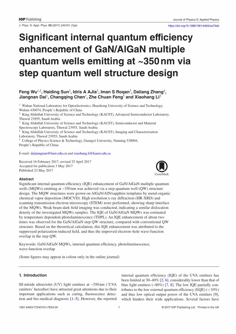
Figure 1(b) shows the AFM image of Sample C, as an example. It is found that all the three samples have a flat surface morph-ology with the roughness below 0.7 nm. Inset in figure 1(b) is the enlarged AFM image showing the step flow surface of the sample, which further demonstrates the good morphology of the samples. Figure 1(c) shows the XRD 2θ − ω spectra of the investigated samples. At least five negative and two posi-tive satellite peaks can be observed for all the samples, indi-cating good material quality and low interfacial roughness of the MQWs. Furthermore, the FWHMs of the satellite peaks are almost equal, showing that the dislocation densities of MQWs are nearly the same for the three samples. The thick-nesses of QW and QB layers based on the XRD simulation are summarized in table 1, which represent a small and accept-able deviation from the designed values. Figure 1(d) shows the asymmetric (1 0 5) reciprocal space mapping (RSM) of Sample C exemplarily. It is noted that the peak of MQWs is vertically aligned with that of AlGaN template layer but has a gap from the peak of AlN layer in horizontal direction, which means that the AlGaN template layer was relaxed and the MQWs were pseudomorphologically grown and fully strained on the AlGaN template layer.
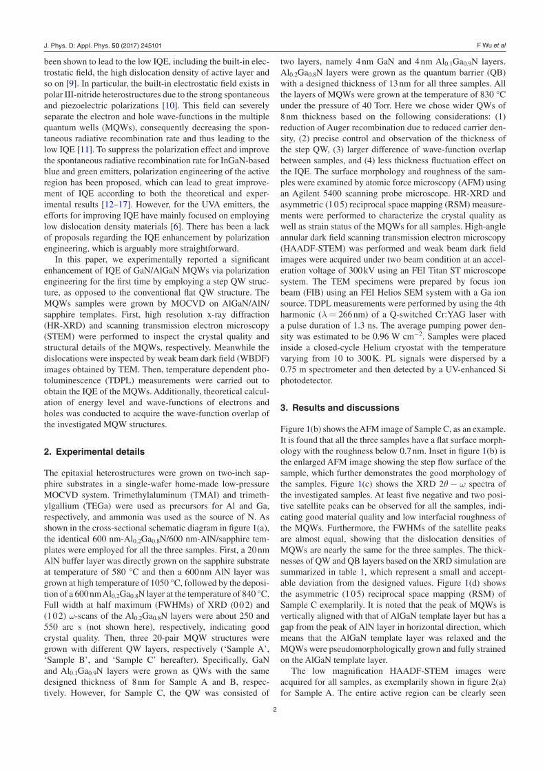
The low magnification HAADF-STEM images were acquired for all samples, as exemplarily shown in figure 2(a) for Sample A. The entire active region can be clearly seen
J. Phys. D: Appl. Phys. 50 (2017) 245101
F Wu et al
3
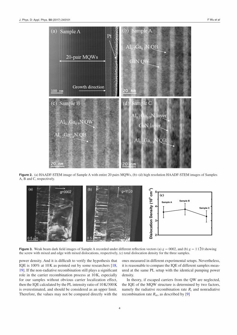
with uniform thickness for both QW and QB layers. To obtain the thickness of each layer, high resolution HAADF-STEM images were acquired for Samples A, B and C, which are shown in figures 2(b)–(d), respectively. All the samples show a very sharp interface between QW and QB, and no obvious thickness fluctuation can be observed. Specifically, the GaN and Al0.1Ga0.9N layers with different contrasts can be dis-tinguished for the QW of Sample C (figure 2(d)), which is consistent with the designed GaN/AlGaN step QW structure. The bright spots in the STEM image of Sample B shown in figure 2(c) may be caused by the Ga ion contamination during the specimen preparation. The thicknesses of QW and QB layers are obtained and summarized in table 1, which represent an insignificant variation from the ones obtained by the XRD measurement. Weak beam dark field (WBDF) TEM images were acquired under different reflection vec-tors g to observe the dislocations in the MQWs active region. According to the visible criterion, screw and mixed disloca-tions can be seen under g = 0002, whereas edge and mixed dislocations are visible under g = 1 1 2 0. Figures 3(a) and (b) show the WBDF TEM images of Sample A exemplarily. It is found that most of the dislocations in MQWs active region are mixed type dislocations. Furthermore, the total dislocation densities are in the same level, ~3.5 × 109 cm−2 for the three
samples, as shown in figure 3(c), which is consistent with the XRD FWHM results.
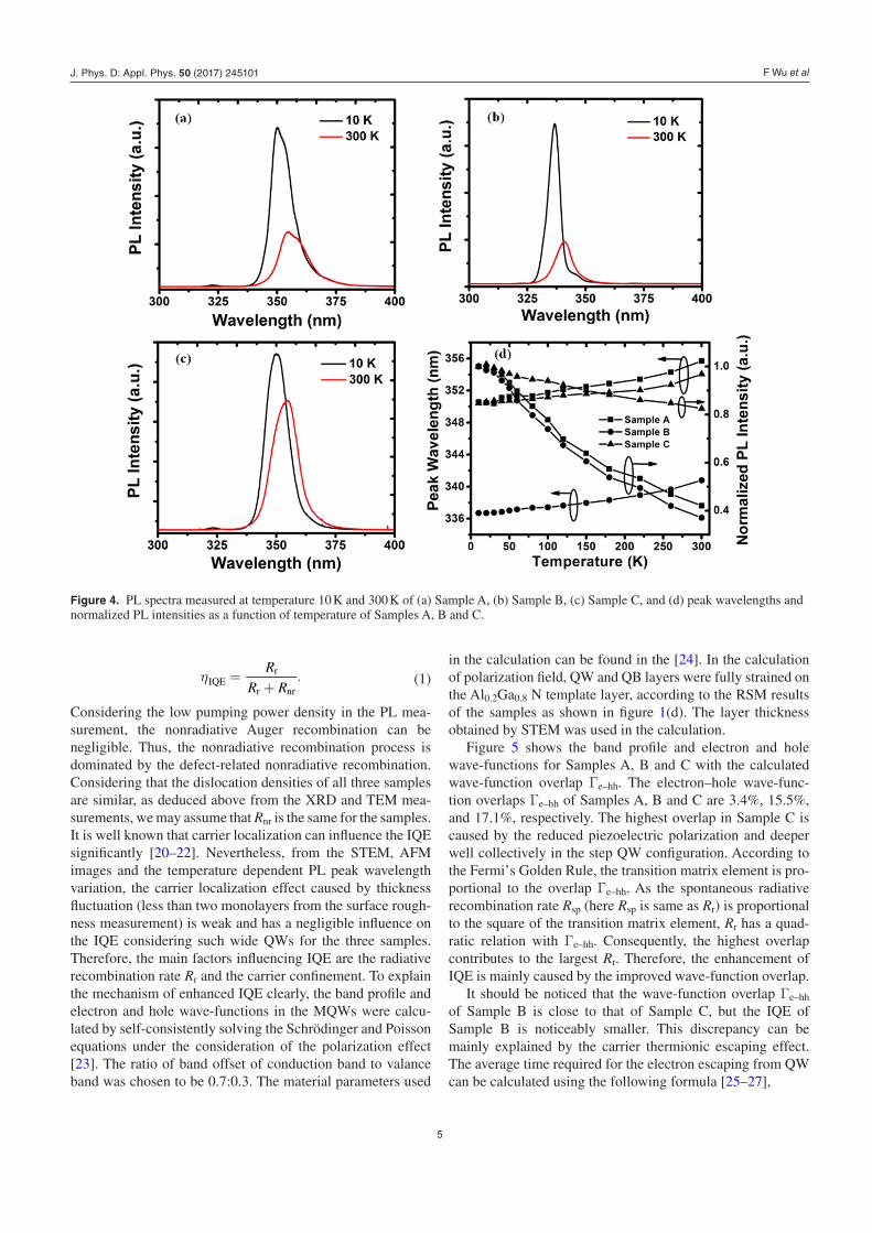
Figures 4(a)–(c) show the PL spectra measured at 10 and 300 K of Samples A, B, and C, respectively. A single emission peak with narrow linewidth below 10 nm can be seen for the three samples. The PL intensity decreases slowly and spec-trum broadens slightly when increasing temperature from 10 to 300 K. Figure 4(d) shows the peak wavelengths and nor-malized PL intensities as a function of temperature for the three samples. The peak wavelength redshifts for all samples with increased temperature from 10 to 300 K because of the temperature induced bandgap shrinkage effect. No obvious ‘S’ shape behavior of the temperature dependent PL peak wavelength variation can be seen for the three samples, which means the carrier localization effect is weak. Here, the IQE of MQWs is estimated by the ratio of integrated PL intensity at 300 K to that at 10 K, under the hypothesis that the non-radia-tive recombination freezes out at 10 K [18, 19]. The estimated IQEs for Sample A, B and C are 42.1%, 37.1%, and 82.4%, respectively, as summarized in table 1. Obviously, Sample C with the step QW structure possesses the largest IQE, which represents a significant enhancement factor of 1.96 and 2.22 over Samples A and B, respectively. It is important to note that the IQE determined by TDPL often varies with the pumping
Figure 1. (a) Cross-sectional schematic diagram of the MQW structures with three different quantum wells of Samples A, B and C, (b) AFM image of Sample C indicating RMS surface roughness of 0.50 nm, inset is the enlarged AFM image, (c) 2θ − ω XRD spectra of Samples A, B and C, and (d) asymmetric (1 0 5) plane reciprocal space mapping of Sample C.
J. Phys. D: Appl. Phys. 50 (2017) 245101
F Wu et al
4
power density. And it is difficult to verify the hypothesis that IQE is 100% at 10 K as pointed out by some researchers [18, 19]. If the non-radiative recombination still plays a significant role in the carrier recombination process at 10 K, especially for our samples without obvious carrier localization effect, then the IQE calculated by the PL intensity ratio of 10 K/300 K is overestimated, and should be considered as an upper limit. Therefore, the values may not be compared directly with the
ones measured in different exper imental setups. Nevertheless, it is reasonable to compare the IQE of different samples meas-ured at the same PL setup with the identical pumping power density.
In theory, if escaped carriers from the QW are neglected, the IQE of the MQW structure is determined by two factors, namely the radiative recombination rate Rr and nonradiative recombination rate Rnr, as described by [9]
Figure 2. (a) HAADF-STEM image of Sample A with entire 20 pairs MQWs, (b)–(d) high resolution HAADF-STEM images of Samples A, B and C, respectively.
Figure 3. Weak beam dark field images of Sample A recorded under different reflection vectors (a) g = 0002, and (b) g = 1 1 2 0 showing the screw with mixed and edge with mixed dislocations, respectively, (c) total dislocation density for the three samples.
J. Phys. D: Appl. Phys. 50 (2017) 245101
F Wu et al
5
η =+R
R R.IQE
r
r nr (1)
Considering the low pumping power density in the PL mea-surement, the nonradiative Auger recombination can be negligible. Thus, the nonradiative recombination process is dominated by the defect-related nonradiative recombination. Considering that the dislocation densities of all three samples are similar, as deduced above from the XRD and TEM mea-surements, we may assume that Rnr is the same for the samples. It is well known that carrier localization can influence the IQE significantly [20–22]. Nevertheless, from the STEM, AFM images and the temperature dependent PL peak wavelength variation, the carrier localization effect caused by thickness fluctuation (less than two monolayers from the surface rough-ness measurement) is weak and has a negligible influence on the IQE considering such wide QWs for the three samples. Therefore, the main factors influencing IQE are the radiative recombination rate Rr and the carrier confinement. To explain the mechanism of enhanced IQE clearly, the band profile and electron and hole wave-functions in the MQWs were calcu-lated by self-consistently solving the Schrödinger and Poisson equations under the consideration of the polarization effect [23]. The ratio of band offset of conduction band to valance band was chosen to be 0.7:0.3. The material param eters used
in the calculation can be found in the [24]. In the calculation of polarization field, QW and QB layers were fully strained on the Al0.2Ga0.8 N template layer, according to the RSM results of the samples as shown in figure 1(d). The layer thickness obtained by STEM was used in the calculation.
Figure 5 shows the band profile and electron and hole wave-functions for Samples A, B and C with the calculated wave-function overlap Γe–hh. The electron–hole wave-func-tion overlaps Γe–hh of Samples A, B and C are 3.4%, 15.5%, and 17.1%, respectively. The highest overlap in Sample C is caused by the reduced piezoelectric polarization and deeper well collectively in the step QW configuration. According to the Fermi’s Golden Rule, the transition matrix element is pro-portional to the overlap Γe–hh. As the spontaneous radiative recombination rate Rsp (here Rsp is same as Rr) is proportional to the square of the transition matrix element, Rr has a quad-ratic relation with Γe–hh. Consequently, the highest overlap contributes to the largest Rr. Therefore, the enhancement of IQE is mainly caused by the improved wave-function overlap.
It should be noticed that the wave-function overlap Γe–hh of Sample B is close to that of Sample C, but the IQE of Sample B is noticeably smaller. This discrepancy can be mainly explained by the carrier thermionic escaping effect. The average time required for the electron escaping from QW can be calculated using the following formula [25–27],
Figure 4. PL spectra measured at temperature 10 K and 300 K of (a) Sample A, (b) Sample B, (c) Sample C, and (d) peak wavelengths and normalized PL intensities as a function of temperature of Samples A, B and C.
J. Phys. D: Appl. Phys. 50 (2017) 245101
F Wu et al
6
⎛⎝⎜
⎞⎠⎟τ
π=
∗ −m L
k T
E E
k T
2expw
T
2
B
c 1
B (2)
where m* is the effective mass of electron, Lw is the thick-ness of quantum well, Ec is conduction band of quantum barrier, E1 is the first energy level in the quantum well, and kB is Boltzmann constant. The binding energy of the exciton in such wide GaN MQWs is around 15 meV [28], much smaller than the thermal energy of 26 meV at room temper-ature, which means that most of the excitons will dissociate at room temperature. Thus, the excitonic effect is weak and not taken into account in the calculation. The calculated escaping time for electrons are 38, 0.04 and 1.6 ns for Samples A, B, and C, respectively. The huge difference of escaping time is caused by the relative large difference of barrier height for electrons in the three samples. Obviously, Sample B has the shortest escaping time due to the lowest barrier height between QW and QB. At the first glance, we may conclude that most of the carriers will escape into QB, resulting in a very low IQE, especially for Sample B, which is not the case here. This is probably because the recapture of carriers into the QWs cannot be dismissed, which means that the escaping effect is not as severe as indicated by the short escaping time. Nevertheless, we can conclude that the escaping effect is more severe for Sample B compared with Sample C, thus resulting in a lower IQE though its electron–hole wave-func-tion overlap is only 1.6% less than that of Sample C. Another possible reason for the lower IQE of Sample B may be the higher emission energy of the AlGaN active region. Based on a previous report, the PL intensity decreased and the low-temperature PL decay lifetime increased with the increase of Al content of the AlGaN film [29]. Thus, a lower IQE maybe expected for Sample B. Moreover, as shown in figure 3(c), the dislocation density of Sample B is a little higher than the
other two samples, which may also contribute to the lower IQE. The results of this investigation indicate that we can obtain a higher electron–hole wave-function overlap Γe–hh and a relative strong carrier confinement simultaneously by using step MQWs with a significantly enhanced IQE as dem-onstrated in Sample C.
4. Conclusions
In summary, we have experimentally demonstrated a signifi-cant enhancement of the IQE of GaN/AlGaN MQWs emitting at ~ 350 nm by approximately two times through suppressing the polarization effect via using the step QW, compared with conventional QW in the active region. XRD and TEM char-acterizations show that the significant difference of the IQE cannot be attributed to the difference of defect-related nonra-diative recombination rate based on the fact that the disloca-tion densities are similar for all samples. The enhancement of IQE of the step MQWs is mainly caused by the increased radiative recombination rate, which results from the improved electron–hole wave-function overlap Γe–hh based on the theor-etical calculation results. The use of controlled polarization to enhance the Γe–hh of GaN based active region can be appli-cable for high-efficiency electrically-injected UVA LEDs and low threshold UV lasers.
Acknowledgments
This work was supported by KAUST Startup and Base-line Funds (Grant No. BAS/1/1664/01-01); National Key R&D Program of China (Grant No. 2016YFB0400901, 2016YFB0400804); National Basic Research Program of China (Grant No. 2012CB619302); Key Laboratory of infra-red imaging materials and detectors, Shanghai Institute of
Figure 5. Band profile and electron and hole wave-functions in QW with calculated wave-function overlap Γe–hh of (a) Sample A, (b) Sample B, (c) Sample C.
Table 1. Layer thickness, IQE and wave-function overlap for the three samples.
Sample IDWell thickness (nm)
Step well thickness (nm)
Barrier thickness (nm)
IQE (measured) (%)
Γe–hh (calculated) (%)
Sample A 8.5/7.94 Not applicable 12.6/11.89 42.1 3.4Sample B 7.4/7.05 Not applicable 12.6/11.67 37.1 15.5Sample C 4.1/4.04 3.9/3.91 12.6/11.60 82.4 17.1
Note: the values in front of ‘/’ were obtained by XRD and the ones behind were obtained by TEM.
J. Phys. D: Appl. Phys. 50 (2017) 245101
F Wu et al
7
Technical Physics, Chinese Academy of Sciences (Grant No. IIMDKFJJ-15-07); National Natural Science Foundation of China (Grant No. 61675079, 11574166, 61377034), and the Director Fund of WNLO.
References
[1] Han J, Crawford H M, Shul R J, Figiel J J, Banas M, Zhang L, Song Y, Zhou H and Nurmikko A V 1998 Appl. Phys. Lett. 73 1688
[2] Yoshida H, Kuwabara M, Yamashita Y, Uchiyama K and Kan H 2010 Appl. Phys. Lett. 96 211122
[3] Morita D, Sano M, Yamamoto M, Murayama T, Nagahama S and Mukai T 2002 Japan. J. Appl. Phys. 41 L1434
[4] Lee Y, Wang T, Liu Y, Ao J, Izumi Y, Lacroix Y, Li H, Bai J, Naoi Y and Sakai S 2002 Japan. J. Appl. Phys. 41 4450
[5] Sun H and Moustakas D T 2014 Appl. Phys. Express 7 012104
[6] Ban K, Yamamoto J, Takeda K, Ide K, Iwaya M, Takeuchi T, Kamiyama S, Akasaki I and Amano H 2011 Appl. Phys. Express 4 052101
[7] Narukawa Y, Narita J, Sakamoto T, Yamada T, Narimatsu H, Sano M and Mukai T 2007 Phys. Status Solidi A 204 2087
[8] Narukawa Y, Ichikawa M, Sanga D, Sano M and Mukai T 2010 J. Phys. D: Appl. Phys. 43 354002
[9] Kneissl M and Rass J 2016 III-Nitride Ultraviolet Emitters (Berlin: Springer)
[10] Ambacher O et al 2000 J. Appl. Phys. 87 334[11] Nardelli B M, Rapcewicz K and Bernholc J 1997
Appl. Phys. Lett. 71 3135
[12] Arif A R, Ee Y and Tansu N 2007 Appl. Phys. Lett. 91 091110[13] Arif A R, Zhao H, Ee Y and Tansu N 2008 IEEE J. Quantum
Electron. 44 573[14] Zhao H, Liu G, Li X, Huang G, Poplawsky D J, Penn T S,
Dierolf V and Tansu N 2009 Appl. Phys. Lett. 95 061104[15] Park S, Ahn D and Kim J 2009 Appl. Phys. Lett. 94 041109[16] Zhao H, Liu G, Zhang J, Poplawsky D J, Dierolf V and
Tansu N 2011 Opt. Express 19 A991[17] Li H, Li P, Kang J, Li Z, Zhang Y, Li Z, Li J, Yi X, Li J and
Wang G 2013 Appl. Phys. Express 6 052102[18] Watanabe S, Yamada N, Nagashima M, Ueki Y, Sasaki C,
Yamada Y, Taguchi T, Tadatomo K, Okagawa H and Kudo H 2003 Appl. Phys. Lett. 83 4906
[19] Shatalov M, Yang J, Sun W, Kennedy R, Gaska R, Liu K, Shur M and Tamulaitis G 2009 J. Appl. Phys. 105 073103
[20] Mickevicius J, Tamulaitis G, Shur M, Shatalov M, Yang J and Gaska R 2012 Appl. Phys. Lett. 101 211902
[21] Jeong H, Jeong H J, Oh H M, Hong C, Suh E K, Leronde G and Jeong M 2015 Sci. Rep. 5 9373
[22] Wang J, Wang L, Zhao W, Hao Z and Luo Y 2010 Appl. Phys. Lett. 97 201112
[23] Wu F, Tian W, Yan W, Zhang J, Sun S, Dai J, Fang Y, Wu Z and Chen C 2013 J. Appl. Phys. 113 154505
[24] Ambacher O et al 2002 J. Phys.: Condens. Matter 14 3399[25] Schneider H and Klitzing V K 1988 Phys. Rev. B 38 6160[26] Lang J, Young N, Farrell M R, Wu Y and Speck S 2012 J
Appl. Phys. Lett. 101 181105[27] Santi D C et al 2016 J. Appl. Phys. 119 094501[28] Grandjean N, Damilano B, Dalmasso S, Leroux M, Laügt M
and Massies J 1999 J. Appl. Phys. 86 3714[29] Kim H, Mair R A, Li J, Lin J and Jiang H 2000