213
siLENT 700 electronic data terminals MANUAL NO. 984025-9701, REV. C REVISED 1 JULY 1978 TEXAS INSTRUMENTS INCORPORATED Model 743 KSR Model 745 Portable Maintenance Manual

siLENT 700 electronic data terminals
MANUAL NO. 984025-9701, REV. C REVISED 1 JULY 1978
TEXAS INSTRUMENTS INCORPORATED
Model 743 KSR Model 745 Portable Maintenance Manual

Copyright 1978 by Texas Instruments Incorporated All Rights Reserved - Printed In USA
The information and/or drawings set forth in this document and all rights in and to Inventions disclosed herem and patents which might be granted thereon disclosing or emploYing the materials, methods, techniques or apparatus described herein are the exclusive property of Texas Instruments Incorporated.
No copies of the information or drawings shall be made without the prior consent of Texas Instruments Incorporated. r--------------------........ INSERT LATEST CHANGED PAGES.DESTROY SUPERSEDED PAGES
LIS T 0 F E F F E C T I V EPA G E S I Note The portIon of the text affected by the changes IS mdlcated by a vertIcal bar ....-__________________ -.-.. In the outer margins of the page.
Models 743/745 Electronic Data Terminals Maintenance Manual
984025-9701, Rev. B Original Issue: 15 December 1975
Totdl numher of pages In thiS publlcatron IS 213 consisting of the following:
Page No.
Revision Letter
A B C
Change No.
Page No.
CHANGE NOTICES ECN
Date Number Level
2-8-77 423767 C 8-22-77 425661 C 6-1-78 439846 0
J
Change No.
Page No.
Description
Update, add drawings and keyboard options Add new printer mechanism and new PWB electronics Correct Katakana keyboard section
Change No.

Section
2
3
TABLE OF CONTENTS
Page
EQUIPMENT DESCRIPTION
1. 1 Scope. . . . . . . . . . . . . . . . . . . . .. 1-1 1.2 References ................... 1-1 1.3 General Description ............. 1-1 1.3.1 Model 743 ........ " ......... 1-1 1.3.2 Model 745 .................. 1-1 1.4 0 pti ons. . . . . . . . . . . . . . . . . . . . . 1-1 1.4.1 Options Available on Both
Models 743 and 745 ............ 1-1 1.4.2 Model 743 Options ............ 1-3 1.4.3 Model 745 Options ............ 1-3 1.5 Physical Dimensions ............. 1-4 1.6 Environmental Limits ............ 1-4 1.6.1 Nonoperating Environment. " ..... 1-4 1.6.2 Operating Environment ......... 1-4
EQUIPMENT INSTALLATION
2.1 Preliminary Checkout ............ 2-1 2.2 Power Connection .............. 2-1 2.3 Communications
Interconnections .......... \.' .. ' .. 'i2~ 1'~ 2.3.1 Acoustic Coupler Configuration,
Model 745 .................. 2-1 2.3.2 EIA Configuration, Model 743 ..... 2-3 2.3.3 TTY Configuration, Model 743 ... : 2-4 2.3.4 Internal Modem Configuration,
Model 743 ........... .': ... : . 2-5 2.3.5 Auxiliary EIA Configuration ..... : 2-5 2.4 Loading Paper. ................ 2-7 2.5 Adjustments ..... " ..... ; ....... 2-7 2.5.1 Print Contrast ................ 2-7 2.5.2 Acoustic Coupler and Modem
Adjustmen'ts. . . . . . . . . . . . . . . . . 2-7
THEORY OF OPERATION 3.1 Functional Description ........... 3-1 3.2 Control Electronics ............. -3-2 3.2.1 Communications Discipline ....... 3-2 3.2.2 Speed ..................... 3-2 3.2.3 Buffering ............ : ...... 3-2 3.2.4 Character Structure ............ 3-2 3.2.5 Parity .............. ' ....... 3-5 3.2.6 Duplex Operation ............. 3-5 3.2.7 Answer-Back Memo'ry Option ..... 3-5 3.2.8 Keyboard Scan ............... 3-5 3.2.9 Mechanism Control ............ 3-5 3.3 Printer Mechanism .............. 3-6
Section
iii
Page
3.3.1 Character Spacing ............. 3-6 3.3.2 Line Spacing ................. 3-6 3.3.3 Paper Supply ............... _ 3-6 3.3.4 Paper Loading ................ 3-6 3.3.5 Paper Tearoff ................ 3-6 3.3.6 Printhead Pressure ............. 3-6 3.4 Printhead System . . . . . . . . . . . . . . 3-6 3.4.1 Printhead Address Drivers ........ 3-6 3.4.2 Temperature Compensation
Circuit ..................... 3-6 3.4.3 Print Voltage Circuit ........... 3-7 3.5 Mechanism Drive Electronics ....... 3-9 3.5.1 Motor Drive Electronics ......... 3-10 3.5.2 Solenoid Drivers .............. 3-13 3.6 Keyboards ................... 3-14 3.6.1 Standard Keyboard ............ 3-14 3.6.2 Optional Full-ASCII Keyboard ..... 3-14 3.6.3 Receive-Only Control Panel ....... 3-20 3.6.4 APL/ASCII Keyboard .......... 3-20 3.6.5 Katakana Keyboard ............ 3-23 3.7 Operator Controls and
Indicators ................... 3-25 3.8 Power Supply ................. 3-25 3.8.1 Power Transformer ............ 3-26 3.8.2 Voltage Regulator ............. 3-27 3.8.3 Failure Protection ............. 3-28 3.8.4 Soft Start Circuit .............. 3-28 3.8.5 Electromagnetic Interference
(EMI) Filter .................. 3-28 3.8.6 Electrical Power Interface ........ 3-28 3.9 Current Loop Interface ........... 3-28 3.9.1 Receiver Circuit .............. 3-28 3.9.2 Transmit Circuit .............. 3-29 3.10 Firmware ................... 3-30 3.10.1 Power-Up Routine ............ 3-33 3.10.2 Keyboard Routine ............ 3-33 3.10.3 Receiver Routine ............. 3-34 3.10.4 Data Control Routine .......... 3-34 3.10.5 Character Analyzer ........... 3-35 3.10.6 Character Buffering ........... 3-36 3.10.7 Paper Advance Operation ....... 3~39
3.10.8 Answer-Back Memory ......... 3-39 3.10.9 Left Margin/Paper-Out
Detection .................. 3-39 3.11 Acoustic Coupler/Modem ........ 3-40 3.11.1 Receiver Section ............. 3-41 3.11.2 Transmitter Section ........... 3-43

TABLE OF CONTENTS, (CONTINUED)
Section
4
Page
MAl NTENANCE 4.1 Preventive Maintenance .......... 4-1 4.2 Troubleshooting ............... 4-1 4.3 Adjustments .................. 4-1 4.3.1 Pri nt Contrast. . . . . . . . . . . . . . . . 4-1 4.3.2 Acoustic Coupler or Modem
Transmit Adjustment ........... 4-3 4.3.3 Printer Subsystem Adjustments .... 4-3 4.4 Su bassembly Replacement . . . . . . . . 4-6 4.4.1 Outer Cover Removal
(Model 745 Only) ............. 4-6 4.4.2 Outer Cover Installation
(Model 745 Only) ............. 4-6 4.4.3 I nner Cover Removal (Both
Mode"ls) .................... 4-6 4.4.4 Inner Cover Installation ......... 4-6
Section
APPENDIX
Page
4.4.5 Mechanism Removal 4-7 4.4.6 Mechanism Installation .......... 4-7 4.4.7 Keyboard Removal ............ 4-7 4.4.8 Keyboard Installation. . . . . . . . . . . 4-8 4.4.9 Fan Removal and Installation ..... 4-8 4.4.10 PWB Removal. .............. 4-8 4.4.11 PWB Installation. . . . . . . . . . . . . 4-8 4.4.12 Printhead Removal ........... 4-8 4.4.13 Printhead Installation .......... 4-8 4.4.14 Option PROM Replacement ..... 4-9
Assembly Drawings and Lists of Material and Electronic Schematics
LIST .oF ILLUSTRATI.oNS
Figure No. Page Figure No. Page
1-1 Models 743/745 Data Terminals ........ 1-2 3-8 Feedback Sensor Light Path Schematic ..................... 3-12
2-1 Major Components & Controls 3-9 Feedback Sensor 02, 03 Circuit
(typical) ...................... 2-2 Schematic ..................... 3-12 2-2 Model 743 TTY Configurations ........ 2-4 3-10 APL and ASCII Character Set 2-3 EIA/Auxiliary Coupler Connections Generation ..................... 3-15
for the Model 745 ................ 2-6 3-11 Katakana and ASCII Character Set 2-4 Auxiliary EIA Modem Connections Generation ..................... 3-16
for the Model 743 ................ 2-8 3-12 Standard Keyboard ,Layout and 2-5 Paper Loading Diagram .............. 2-9 Symbolization .................. 3-17
3-13 Code Generating Keys With No Mode 3-1 Models 743/745 Simplified Block Keys Depressed .................. 3-17
Diagram ....................... 3-1 3-14 Code Generating Keys With CRTL 3-2 Serial Data Timing Diagram ........... 3-2 Key Depressed .................. 3-17 3-3 Model 743/745 Printing Su bsystem 3-15 Code Generating Keys With Numbers
Block DiagrClm .................. 3-7 Key Depressed .................. 3-18 3-4 Printhead Matrix and Address Lines, and 3-16 Code Generating Keys With Shift
Printhead Element Block Diagram ..... 3-8 Key Depressed .................. 3-18 3-5 Printhead Interface Timing (For 3-17 Optional Full-ASCII Keyboard
Letter "F") .................... 3-9 Layout and Symbolization .......... 3-18 3-6 Motor Drive Circuit Block Diagram ...... 3-10 3-18 Codes Generated With No Mode 3-7 Motor Drive Circuit Feedback Sensor Keys Activated .................. 3-19
Output Characteristics ............. 3-11 3-19 Codes Generated With the SHIFT ' Key Pressed and Held .............. 3-19
iv

LIST OF ILLUSTRATIONS (CONTINUED)
Figure No.
3-20
3-21 3-22
3-23
3-24
3-25
3-26
3-27
3-28
3-29
3-30
3-31
3-32
3-33
3-34
Page
Codes Generated With the CTR L Key Pressed and Held ................. 3-19
Receive-Only Control Panel ........... 3-20 Optional APL Keyboard Layout and Symbol ization ................... 3-20 Codes Generated in the APL Mode with no Mode Keys Activated (APL Keyboard) ... 3-21 Codes Generated in the APL Mode with the
SHIFT Key Pressed and Held(APL Keyboard) ..................... 3-21
Codes Generated in the ASCII Mode with no Mode Keys Activated (APL Keyboard)3-21
Codes Generated in the ASCII Mode with the SH I FT Key Pressed and Held (APL Keyboard) ................. 3-22
Codes Generated in the ASCII Mode with the CTR L Key Pressed and Held (APL Keyboard) ................. 3-22
Katakana Keyboard Layout and Symbolization .................. 3-23
Katakana Keyboard Codes Generated in the Unshifted Kana Mode ......... 3-24
Katakana Keyboard Codes Generated in the Kana Mode with SH I FT Pressed and Held ................. 3-24
Katakana Keyboard Codes Generated in the Unshifted Alpha Mode ......... 3-24
Katakana Keyboard Codes Generated in the Alpha Mode with SHIFT Pressed and Held ................. 3-25
Katakana Keyboard Codes Generated with the CTR L Key Pressed and Held ... 3-25
Model 743/745 Power Supply Functional Block Diagram ........... 3-26
Figure No.
3-35
3-36
3-37
3-38 3-39
3-40
3-41 3-42
3-43
3-44
3-45
4-1
4-2
4-3
4-4
Page
Transient Surge ac Voltage Step Function Loci Limits for 110 Vac Operation ..... 3-29
Model 743/745 Firmware Control System Block Diagram ............. 3-30
Functional Block Diagram I/O and Timer Device ................... 3-31
Model 743/745 Firmware Structure ..... 3-32 Model 743/745 Keyboard Matrix
Encoding Scheme ................ 3-33 ' J
Models 743/745 Print/Step Routine Pulse Train ..................... 3-35
Print/Step Routine State Diagram ....... 3-37 Stepping Motor Line Feed (LF) Routine
Timing Diagram ................. 3-38 Carriage Return Routine State
Diagram ....................... 3-30 Frequency-Shift Keying (FSK)
Modulation .................... 3-40 Acoustic Coupler/Modem Block
Diagram ....................... 3-33
Models 743/745 Component Locations. . . . . . . . . . . . . . . . . . . . . . 4-2
Module Connectors and Printhead Components .................... 4-4
Printhead Adjustments and Components .................... 4-5
Power Cord Storage in 745 Outer Cover ....................... .4-11
Troubleshooting Flow Diagrams ....... .4-12
LIST OF TABLES
Table No. Page
1-1 Options for the Models 743/745
2-1
2-2
Data Terminals .................. 1-3
External Interface Connector Pin Assignments ................. 2-3
Model 743 EIA Interface Cable Pin Assignments. . . . . . . . . . . . . . . . . . . . 2-3
v
T able No. Page
2-3 Teletype Current Loop Cable Pin
2-4
2-5
2-6
Assignments. . . . . . . . . . . . . . . . . . . . 2-4 Options Internal Modem Cable Pin
Assignments. . . . . . . . . . . . . . . . . . . . 2-5 EIA/Auxiliary Acoustic Coupler Cable
Pin Assignments Model 745 .......... 2-6 EIA/Auxiliary Modem Cable Pin
Assignments for Model 743 .......... 2-8
LIST OF TABLES (CONTINUED)
Table No. Page Table No. Page
3-1 APL and ASCII Code System and 3-5 Acoustic Coupler FSK Transmission Character Set. . . . . . . . . . . . . . . . . . . 3-3 Frequency Assignments ............ 3-41
3-2 Katakana and ASCII Code System and Character Set. . . . . . . . . . . . . . . . . . . 3-4 4-1 Models 743/745 Optional Internal
3-3 Power Supply dc Output ............. 3-26 Electronics Jumpers ............... 4·9 3-4 Firmware Operating System 4-2 Keyboard Kit and Option PROM
Interrupts ..................... 3-32 Replacement Part Numbers .......... 4·9
vi

SECTION I
EQUIPMENT DESCRIPTION
1.1 SCOPE. This manual contains descriptions, installation instructions, theory of operation, and maintenance procedures for the Silent 700* Models 743 and 745 Electronic Data Terminals manufactured by the Digital Systems Division of Texas I nstruments I ncorporated. The information in this manual is intended to help in maintaining and servicing these data terminals. The troubleshooting data is designed to hel p isolate problems to one of the five major assemblies.
A general description of the Models 743/745 and available options Is included in th is section of the manual. Necessary interfacing and installation information is contained in Section 2, and a general theory of operation is included in Section 3. Maintenance and troubleshooting procedures are contained in Section 4. Lists of materials, related mechanical drawings, and electrical schematics are included in the appendix to this manual.
1.2 REFERENCES. Other TI manuals concerning the Models 743/745 Data Terminals include:
• Model 743 Operating Instructions, TI Part No. 984030-9701
• Model 745 Operating Instructions, TI Part No. 984024-9701.
1.3 GENERAL DESCRIPTION. The Silent 700* Models 743/745 Electronic Data Terminals are self-contained, compact, durable machines designed for use in a wide variety of telecommunications systems. Silent electronic printing is achieved using a five-by-seven-dot matrix mounted on a monolithic, solid-state printhead which prints up to 80 characters across the page. The dot matrix is composed of 35 individual, solid-state heating elements, each electronically controlled. Voltage is applied to the appropriate elements in the matrix for each printable character. The thermal energy thus generated is transferred to heat-sensitive paper, creating a visible image.
*Tradem«k of Texas Instruments Incorporated
1-1
The standard Models 743 and 745 feature a 58-key, TTY 33-compatible, modular keyboard with integral numeric keypad, carrier-detect indicator, two-key rollover, and key debounce circuitry. Various optional keyboards are described in Section 1.4.
Both models are designed and built using snap-in, quick replacement modules for fast, simple, field maintenance. The primary modules include the case, keyboard, printhead and paper drive mechanism, cooling fan, and the printed-wiring board (PWB)
which contains all electronics.
1.3.1 MODEL 743. The TI Model 743 Data Terminal, shown in Figure 1-1, is a light-weight, table-top electronic-printing data terminal capable of operating in full- or half-duplex modes at 10 or 30 characters per second. The Model 743 uses a character set and code compatible with the American Standard Code for Information Interchange (ASCII). The standard communications interface provided with this model is the EIA RS-232-C.
1.3.2 MODEL 745. The TI Model 745 Portable Data Terminal, shown in Figure 1-1, is a light-weight, portable, electronic-printing data terminal with a built-in acoustic coupler and integral carrying case. The Model 745 is capable of operating in full- or half-duplex modes at 10 or 30 characters per second, using a character set and code compati ble with the American Standard Code for Information Interchange (ASCII). The Model 745 is designed to use standard
commercial telephone facilities for interrogation of computerized data bases from a remote location.
1.4 OPTIONS. Several options are available for both the Model 743 and 745, but some options may be used on only one model. Options for both models are listed in Table 1-1.
1.4.1 OPTIONS AVAILABLE ON BOTH MODELS 743 AND 745. The following options are available for
both models.

1.4.1.1 Answer-Back Memory. The optional Answer
Back Memory configuration provides a customer
specified, 1- to 21-character identification sequence
which is transmitted to the communications line upon receipt of the ENQ code from the line Or upon actuation of the HERE IS key by the operator. In
addition to the character sequence, the customer also
specifies whether or not the transmitted sequence of characters is printed if the terminal is in the half
duplex mode. The answer-back contents are not
printed when the terminal is off-line and the ENQ
code is received.
1.4.1.2 Parity Options. The standard Models 743 and
745 are shipped with even parity for transmitted
data. Factory-installed odd, mark, or space parity is
ava ilable as specified in the original purchase order.
1.4.1.3 Full-ASCII Keyboard. An optional Full-ASCII
keyboard is available for both Models 743 and 745.
This keyboard transmits, receives, and prints both
uppercase and lowercase alphabet characters using the
SH I FT key as on a standard typewriter. A special
UPPER CASE rocker switch is provided to permit
generating/printing uppercase-only alphabet char
acters.
P1000032a&1: Figure 1-1. Models 743/745 Data Terminals
1-2

Table 1-1. Options for the Models 743/745 Data Terminals
l Available For:
Option I Model 743 I Model745
Acoustic Coupler No Yes (standard)
Auxiliary Use of No Yes Acoustic Coupler
Internal Modem Yes No
Auxiliary Use of Modem Yes No
EIA RS-232-C Yes Yes*
EIA 103A/113A Yes No
TTY Half Duplex Yes No
TTY Full Duplex Yes No
European (CCITT) No Yes Acoustic Coupler
Answer-Back Yes Yes Memory
Full-ASCII Keyboard Yes Yes
Receive-only Keyboard Yes Yes
APL/ASCII Keyboard Yes Yes
Katakana Keyboard Yes Yes
*With Auxiliary Acoustic Coupler
1.4.1.4 APL/ASCII Keyboard. An optional APL/ ASCII keyboard is available for both Models 743 and 745. This keyboard transmits, receives, and prints either in the full-ASCII mode or in the APL mode, depending on the position of the APL/ASCII mode select switch.
1.4.1.5 Receive-Only Option. A receive-only control panel replaces the standard keyboard of either model data terminal. The receive-only Models 743 and 745 are available with the Answer-Back Memory option and limited-ASCII or full-ASCII. The control panel has PAPER ADV and LOW SPEED controls and a carrier-detect indicator.
1.4.2 MODEL 743 OPTIONS. The following options are available only on the Model 743 data terminal.
1.4.2.1 Current Loop Interface. The Current Loop Interface option converts the EIA levels of the basic
1-3
unit into a TTY 33-compatible, current loop interface. This interface may be used in either four-wire or two-wire communications systems. The nominal operating current is 20 milliamps dc. A 6-foot cable terminated in four spade lugs is provided with this option.
1.4.2.2 Internal Modem. The Modem configuration converts the EIA levels of the standard Model 743 to FSK signals for presentation to a Bell-type COT, manual Data Access Arrangement (DAA). When connected to the DAA, the modem is functionally equivalent to a Bell 103A Data Set. It meets all interface requirements of the DAA, including adjustment of the transmit level without removal of any parts. A 6-foot cable, terminating in two spade lugs, is supplied for COT DAA connection.
1.4.2.3 EIA/Auxiliary Modem Cable. The EIA/ Auxiliary Modem Cable for the Model 743 is applicable only to the internal modem configuration. It provides separate EIA interfaces to the keyboard/ printer and to the internal modem, which permits connection of an external device (e.g., tape cassette, plotter, etc.) between the two interfaces. The 6-foot cable supplied provides COT DAA spade lug terminations as well as a 25-pin male connector for terminating the keyboard/printer interface and a 25-pin female connector for terminating the internal modem EIA interface. Both connectors are compatible with the requirements of EIA Specification RS-232-C. With these two connectors mated the terminal functions as described in paragraph 1.4.2.2 above.
1.4.3 MODEL 745 OPTIONS. The following options are available only for the Model 745.
1.4.3.1 EIA/Auxiliary Coupler Interface. The EIA/ Auxiliary Coupler Interface option of the Model 745 prOVides separate EIA interfaces to the internal acoustic coupler and to keyboard/printer functions. This option enables connection of an external device (e.g., tape cassette, plotter, etc.) between the two interfaces. The 6-foot cable supplied provides a 25-pin male connector for terminating the keyboard/printer interface and a 25-pin female connector for terminating the internal acoustic coupler. Both connectors are compatible with the requirements of E IA Specification RS-232-C. With these two connectors plugged together, the terminal functions the same as a basic Model 745.

1.4.3.2 C.C.I.T.T. Acoustic Coupler. The C.C.I.T.T. Acoustic Coupler option converts the EIA'levels of
the basic unit to FSK tones for presentation to a standard commercial telephone handset. The C.C.I.T.T. Acoustic Coupler operates in full duplex mode over switched telephone networks at data rates up to 300 baud in accord with the requirements of C.C.I. T. T. Recommendation VIII, Data Transmission. Like the U.S. acoustic coupler for the basic Model
745, this version operates in the originate mode only:
no signals are transmitted until the carrier signal is received from the answer end of the communication link.
1.5 PHYSICAL DIMENSIONS. The Model 743 Data Terminal is a compact unit designed for desk-top use. The Model 745 Data Terminal is a self-contained unit designed to fit easily beneath a commercial airliner seat. The Model 745 outer structure is built to afford the same protection, from both the elements and physical abuse, as a sturdy attache case.
Size
The overall terminal dimensions (in inches) are
Model 745 Model 743 Depth: 16.0 15.25 Width: 15.4 14.60 Height: 4.6 4.25
Weight
The maximum weight of the Models 743 and 745 terminals with paper is
Model 745 Model 743
13.5 pounds 11.2 pounds.
1.6 ENVIRONMENTAL LIMITS.
1.6.1 NONOPERATING ENVIRONMENT. The terminal, exclusive of the thermal paper, will operate
within the minimum specified performance require
ments after enduring the following environmental
conditions.
In Shipping Container:
1.
2. Relative Humidity: -10% to 95% without
condensation
* Derate upper limit 1 ° C per 1000 feet above 6000 feet altitude.
1-4
3.
4.
5.
6.
Shock: Drop from 40 inches on each surface and corner
Vibration; Sinusoidal, 2G, 5 to 50 Hz; 4G, 50 to 500 Hz; 6-mlnute linear sweep
Altitude: 50,000 feet
Cargo Bounce: per MIL-STD 810B;
1-lnch double amplitude orbital motion,
225 RPM, 30 minutes per side.
Out of Shipping Container:
1.
2.
3.
4.
Relative Humidity: 10% to 95% without condensation
Shock:
Portable model 20G for 11 mill iseconds
Vibration: Sinusoidal 1.5G, 5 to 500 Hz.
1.6.2 OPERATING ENVIRONMENT. The terminals will operate within specifications under the following environmental conditions.
1. Ambient temperature: 10°C to 40°C*
2.
3.
4.
5.
6.
Relative humidity: 10 percent to 90 percent without condensation
Altitude: to 12,000 feet
Vibration: sinusoidal vibration of 0.5G peak In the range of 10 to 60 Hz
Shock: OG
Temperature shock: operate in a 25°C, 50 percent relative humidity environment
within 30 minutes after being stored for 2 hours at _30° C at 50 percent relative humidity.
These specifications apply to equipment hardware;
for paper limitations see TI Paper Specification 972603 (maximum temperature in the vicinity of
paper roll is less than 5° C greater than am bient temperature).

SECTION 2
EQUIPMENT INSTALLATION
2.1 PRELIMINARY CHECKOUT. Visually check the data terminal before applying
power. After unpacking, check for any obvious
shipping damage such as a damaged top cover. Look for packing material inside the mechanism and paper roller. Verify that the inner cover and base fit snugly
together.
NOTE
The printer will not operate without paper on the drive roller since damage to both platen and printhead could result. After loading paper the control logic
should be reset by cycling power off and on or by pressing the carriage RETURN key.
2.2 POWER CONNECTION. The Models 743/745 Data Terminals are manufactured to operate from three-wire 115-Vac power. The power cord plugs into the right rear of the terminal
(see Figure 2-1).
Two power cords are used with the Models 743/745:
•
•
Terminal serial numbers OX743YYYYY
and OX745YYYYY use part number 972674-0001.
Terminal serial numbers OX744YYYYY and OX746YYYYY use part number
996289-0002.
2.3 COMMUNICATIONS INTERCONNEC-TIONS.
The communications interface for the Model 745 Portable is available through the telephone handset muffs located at the top rear of the case.
The external (cable) interface for the Model 743 KSR and for the Model 745 with the EIA/Auxiliary Coupler option is available through a 15-pin connector at the rear of the terminal. Signals available at the external interface connector are defined in Table 2-1.
Specific configuration connections are described in the following paragraphs.
2-1
2.3.1 ACOUSTIC COUPLER CONFIGURATION, MODEL 745. Using the built-in acoustic coupler, the communications link is established as follows.
a. Switch terminal power on and press the carriage RETURN key.
b.
c.
d.
e.
f.
Set the LOW SPE ED rocker switch on the
keyboard to the right for 30 CPS* or to the left for 10 CPS; these rates equal 300
baud and 110 baud, respectively.
Set the transmission mode (HALF DUP)
switch on the keyboard to the HALF (left) or full (right) 0 UPlex mode.
Set the ON LINE switch to the left position.
Lift the telephone handset from the cradle and dial the appropriate number to connect the Model 745 to the data equipment at the other end of the telephone line.
When an audible high-frequency signal (mark) is heard on the receiver, place the
telephone handset into the aco ustic cou
pler muffs so that the telephone handset cord is to the left side of the data terminal. Wait 3 to 7 seconds for the CARRIER DETECT indicator to illuminate.
NOTE
Take special care to insert the handset into the muffs so that the outer lip of each muff mates with the grooves surrounding the handset earpiece and mouthpiece. The removable caps on the handset must be completely surrounded by the inside circumference of the muffs.
g. Begin communication according to your
system instructions.
*CPS = characters per second

ACOUSTIC ~ COUPlER*l
(REAR VIEW)
POWER CORD CONNECTOR --..,;~~
·NOTE: MODEL 745 only
IDENTIFICATION LABEL (MODEL, VOLTAGE, POWER, SERIAL NO.)
Figure 2-1. Major Components and Controls (Typical)
2-2
POWER CORD STORAGIt
OUTER COVER*
ACOUSTIC _" __ ~ COUPLER
MUFFS*
~ PLATEN AND DANCING ROLLER (UNDER PAPER)
CARRIER-DETECT INDICATOR

J403 I Pin No. Source
9 Common Terminal
"C 14 "- Terminal co 15 .8 "[Term;nal > CJ 13 ~ ~ Terminal 12 ~ ~ External
C1l c: ~ -c:
11 ;t External
2 .~ 11 [Term;nal 8 10 of! Terminal
CJ "-._ C1l c: ~ c:
3 E - External E~
6 8 W External
7 External
5 External
4 External
10 Terminal
Table 2-1. External Interface Connector Pin Assignments
I Function
Protective Ground - Connected to terminal chassis and power cord ground Signal Ground - Common return for all data and control lines CR Busy - Low power TTL level, high-true when printhead is lifted (for test only) DTR - EIA level held to ON condition when terminal is on-line XMTD - Transmit data; EIA level held to MARK state when no data is being transmitted RCVD - Receive data; EIA level held to MAR K state by external device when no data is
to be printed CDET - Carrier detect; EIA level held to ON condition by external device when data
is to be received on pin 12 CAROET - Carrier detect; EIA level held to ON condition by terminal when carrier is detected RCVOA TA - Receive data; EIA level held to MARK state by terminal when no data
is being received XMIT DA TA - Transmit data; EIA level held to MARK state by external device when no data
is to be transmitted RL 1 - Input side of receive data current loop when current loop option is installed;
otherwise, 3.3k ohms to +5V RL 2 - Return side of receive data current loop when current loop option is installed;
otherwise, 3.3k ohms to +5V
tOT - Data Tip; DAA signal when modem option is installed X1 - I nput side of transmit data current loop when current loop option is installed OR - Data ring; D~A signal when modem option is installed X2 - Return side of transmit data current loop when current loop option is installed P12V - Spare EIA level held to ON condition when terminal power is on (3.3k ohms to +12V)
NOTES 1. The terminal connector (J403) is a 15-pin (male) plug, AMP PIN 206913-2, or Amp pIN 205867-2, or equivalent. 2. The mating (cable) connector (P1) is a 15-pin (female) receptacle, Amp PIN 205205-1 or equivalent.
h. In the event the communication link is lost during operation, replace the handset into its cradle, and repeat steps e through
9 above.
2.3.2 EIA CONFIGURATION, MODEL 743. A 6-foot cable with a 25-pin male connector (Cannon DB-25P or equivalent) on the modem end and a
mating 15-pin female connector on the data terminal end is provided with the standard EIA interface for the Model 743 terminal. Pin assignments are listed in Table 2-2. Complete the following steps to establish the communications link.
a. Connect the 6-foot cable between the terminal and the data set.
Table 2-2. Model 743 EIA Interface Cable Pin Assignments
103A Data Set (Cable Part No. 983848) l13A Data Set (Cable Part No. 983854)
Pl Connector I P2 Cable I to Modef 743 Termination
P1-9 P2-1 P1-13 P2-2 P1-12 P2-3 P1-1 P2-7 P1-11 P2-8 P1-15 P2-20 Pl-10 P2-4
Cable Function Connector to I Model 743 Termination
Protective Ground P1-9 Transmit Data P1-13 Receive Data P1-12 Signal Ground Pl-1 Data Carrier Detect1 Pl-15 Data Terminal Ready2 Request to Send 3
P1- 1O J P1-ll
NOTES I Must be > +3 V to receive data. 2 FunctIon of ON LINE SWitch: > +3 V when on-line
< -3 V when off-line. 3 > +3 V when power is ON.
2-3
P2-l P2-2 P2-3 P2-7 P2-20
I Function
Protective Ground Transmit Data Receive Data Signal Ground Data Terminal Ready 3
{ Terminal Carrier Detect Biased ON

b. Set the LOW SPEED rocker switch on the
keyboard to the appropriate speed: left
for 10 CPS or right for 30 CPS.
c. Switch terminal power on and press the
RETURN key.
d. Set the ON LI N E switch to the left
position.
e. Begin communications according to your
system instructions.
2.3.3 TTY CONFIGURATION, MODEL 743. A 6-
foot cable (TI Part No. 983850-0001) is provided to
connect the Model 743 to the communication line.
This cable consists of a 15-pin connector for connec
tion at the rear of the terminal, and four spade lugs at
the other end of the cable. Pin assignments are listed
in Table 2-3. Use the following procedure to com
plete the communication link for four-wire (full
duplex) and two-wire (half-duplex).
. Table 2-3. Standard dc-Current Loop
I nterface Cable Pin Assignments (Cable Part No. 983850)
P1 Connector I to Model 743
Cable
Termination I Function
P1-6 RL 1 lug (white wire) 743 Rcv Loop Input
P1-7 RL2 lug (green wire) 743 Rcv Loop Return
P1-5 X 1 lug (black wire) 743 Xm It Loop Input
P1-4 X2 lug (red wire) 743 Xmlt Loop Return
P1-13] P1-3
Transmit Jumper
P1-12] P1-8
Receive Jumper
{Terminal Carrier
Detect blilsed ON P1-11] P1-2
NOTE Signal ground is not required when using
the dc current loop interface, since the
transmit/receive current loop circuitry
utilizes optically coupled isolators.
a. For full duplex mode connect the four wires [Xl and X2 (transmit pair) and
R L 1 and R L2 (receive pair)] to the signal
source as shown in Figure 2-2. For half
duplex operation connect Xl and R L2 to the communication source. Connect X2
to R L 1, thus putting the terminal's trans
mit and receive leads in series as shown in Figure 2-2.
2-4
Full Duplex
1--------, I MODEL 743 Xl I (BLACK)
1 ~~ '>---------4----71
Pl·5
11---' I I
1 1 cS~~~~~T I (XMIT)
I I L ____ .J I I I I 1
I I
(RCV)
X2 I
Pl 4
I RU ,
4 ) Pl 6
I I I
(RED)
(WHITE) "
(GREEN) I RL2 I, >---...... -~ L _______ Pl.7
Half Duplex
IwiO~L ~ - - - - ~1; IBLACK)
I r 4 » '>--~-'---7I I r - - - - -, Pl 5
I I I
1
I
I ~ CURRENT I : I SWITCH I
I L ____ ..J X2 I IRED)
L----~---R .... L-l -'3>P<:4 IWHITE) f Pl 6
I
1 RL2 I IGREEN)
L _____ ~_;,~ •
EXTERNAL RECEIVER
AND CURRENT
SOURCE
EXTERNAL TRANSMITTER
AND CURRENT
SOURCE
EXTERNAL TRANSMITTER!
RECEIVER AND
CURRENT SOURCE
Figure 2-2_ Model 743 TTY Configurations
b.
c.
d.
e.
Set the LOW SPE ED rocker switch to the left position for 10 CPS or to the right
for 30 CPS.
Switch terminal power on and press the
RETURN key.
Set the ON LI N E rocker switch to the
left position.
The terminal should be operable. If not,
check polarity of the leads described in
step a above, and repeat steps b through
d.

2.3.4 INTERNAL MODEM CONFIGURATION, MODEL 743. A 6-foot cable (TI Part No. 983849-0001) terminated in two spade lugs is available for the Model 743. This cable provides standard data tip (DT) and data ring (DR) output/input signals. Pin assignments are listed in Table 2-4. The procedure for completing the communications link is as follows:
a.
b.
c.
Connect the 6-foot cable between the terminal and the COT DAA. See Table
2-4 for pin assignments.
Switch terminal power on and press the
RETURN key.
Set the LOW SPEED rocker switch to the
left position for 10 CPS or to the right
for 30 CPS.
d. Set the 0 N II N E rocker switch to the
left position.
e.
f.
On the telephone, dial the appropriate
number to connect the data terminal to
the data equipment.
When an audible high frequency signal is heard through the receiver, lift the white
data button on the telephone cradle and place the handset on the table beside the dial unit.
Table 2-4. Optional Internal Modem Interface Cable Pin Assignments
(Cable Part No. 983849)
----------~---------.----------~
Pl Connector I Connector to I to Model 743 DAA
Pl-5 lug Ired wire)
Pl-4 lug (black wire)
Pl-13] Pl-3
Pl-12] Pl-8
Pl-ll] Pl-2
Function
Data TIp (OT)
Data Ring (OR)
Transmit Jumper
Receive Jumper
{Carrier Detect
Jumper
2-5
2.3.5 AUXI LlARY MODEM/COUPLER CON
FIGURATION. The Models 743/745 Data Terminals can be equipped with EIA interface capability and auxiliary use of the coupler or modem by use of
either of two optional cables:
•
•
EIA/Auxiliary coupler cable (TI Part No. 983847-0001) for the Model 745.
EIA/Auxiliary modem cable (TI Part No .
983855-0001) for the Model 743.
2.3.5.1 EIA/Auxiliary Coupler, Model 745. In this
application the coupler is used to communicate with
an external device and, therefore, is used separately
from terminal operation. Figure 2-3 diagrams this
mode of operation, and pin assignments are listed in Table 2-5. The link may be completed through use of
the following procedure.
NOTE The Model 745 with the EIA/Auxiliary
Coupler option installed is shipped with
no internal connection between the acoustic coupler and the keyboard/ printer. The jumper connector (TI Part No. 983846) furnished with the EIA/ Auxiliary Coupler option must be inserted into the communications interface connector at the rear of the terminal to permit use of the Model 745 in its standard configuration.
a.
b.
c.
d.
Connect P1 of the 6-foot cable to the
communication interface connector at the rear of the Model 745.
Connect P2 to P3 at the opposite end of the 6-foot cable.
Test terminal operation as though it were a standard Model 745; follow the procedure outlined in Section 2-3.1 above. If this link tests satisfactorily, continue the procedure.
Unplug P2 from P3 and plug P3 into an
external device for auxiliary use of the acoustic coupler. Complete the communications link as described in Section
2-3.1 above.

AOOOI074
KEYBOARD
External Device:
Plotter, Recorder, etc
External Controller.
~.--=-----L_-4 Computer, another terminal, etc.
NOTE The Model 745 with the EIA/Auxiliary Coupler option installed is shipped with no internal connection between the
acoustic coupler and the keyboard/ printer. The jumper connector (TI Part
No. 983846) furnished with the EIA/ Auxiliary Coupler option must be inserted into the communications interface
connector at the rear of the terminal to permit use of the Model 745 in its standard configuration.
Figure 2-3. EIA/Auxiliary Coupler Connections for the Model 745
Table 2-5. EIA/Auxiliary Acoustic Coupler Cable Pin Assignments Model 745 (TI Part No. 983847)
Terminal
I Cable
I Connector Termination Function (P1) (P2 and P3)
Pl-9 P2-l 2! Q) rprotectlve Ground c: u Pl-13 P2-2 0;: co Transmit Data' a.'t Pl-12 P2-3 '- Q) Receive Data' -c ... Pl-l0 P2-4 ~.::~ +12 Volts to RTS',4 Pl-l P2-7 ~<t: Signal Ground'
P2-8 >-
Data Carrier Detect"S P1-1l Q)W
Pl-15 P2-20 ~
>?ata Term I n~1 Ready',' Pl-8 P3-3 (jj
- Q) Receive Data-
Pl-3 P3-2 a. u
Transmit Data O :l III
Pl-l P3-7 o ~ U (jj Signal Ground o
Pl-2 P3-8 .~ E ... Carrier Detect' Pl-9 P3-l ~~ Protective Ground Pl-6 P3-5 o -
u W Clear to Send 2,.
Pl-7 P3-6 <t: Data Set Ready2,.l
NOTES
1 Relative to the keyboard and prmter (P2) 2. Relative to the acoustic coupler mternal to the terminal and on another
connector (P3) 3 DTR IS on (> + 3V) when term mal IS on-Ime 4 EIA on « + 3V) when power IS ON.
5. Held to EIA ON by external equipment reqUired for data reception
2-6
I
e.
f.
Check your external device for satisfactory operation before continuing.
Connect P2 to an external controller. Check the Model 745 keyboard and printer for normal operation.
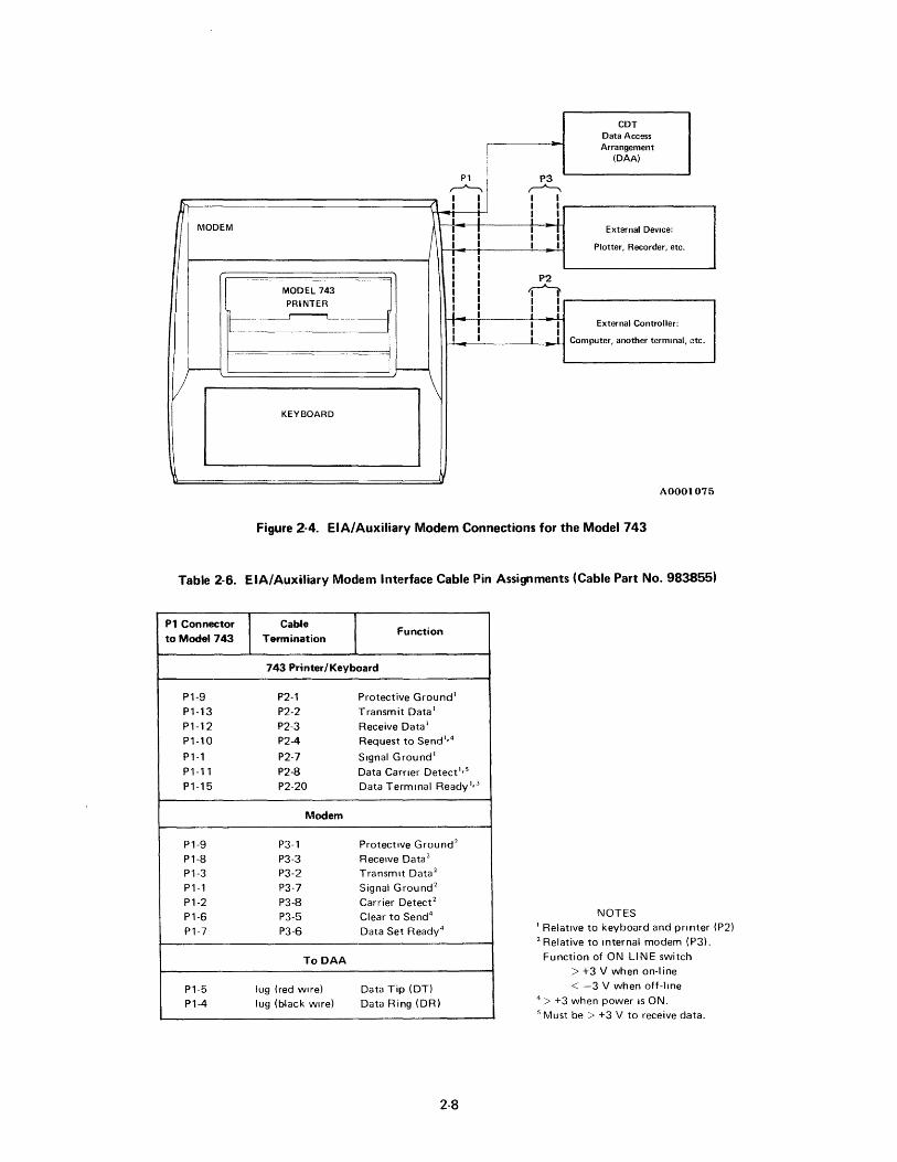
2.3.5.2 EIA/Auxiliary Modem, Model 743. In this application the modem is used with an external device rather than normal terminal functions. Figure 2-4 diagrams this mode of operation. Pin assignments are listed in Table 2-6. The communications link may be completed using the following procedure.
a.
b.
c.
d.
e.
f.
Connect Pl of the 6-foot cable to the communication interface connector at the rear of the Model 743.
Connect the spade lugs to the COT DAA (see Table 2-6).
Connect P2 to P3 and test the Model 743 for normal operations as outlined in Section 2.3.2 above.
After the link has been completed, remove P2 from P3 and connect P3 to an external device.
Test the external device for satisfactory operation.
Connect P2 to an external controller and test the Model 743 printer and keyboard for normal operation (see Section 2.3.2 above).
2.4 LOADING PAPER. The following procedure describes how to load a fresh supply of paper into the Models 743/745. See Figures 2-1 and 2-5 for identification of components.
IMPORTANT NOTE The warranty and/or service contract on the thermal printhead is subject to nullification if the thermal printing paper used in the Silent 700 Data Terminal does not meet TI Specification 972603-0001.
a.
b.
Switch terminal power on.
Open the paper door and remove any excess (old) paper or the empty core from the paper receptacle.
2-7
c.
d.
e.
f.
g.
h.
i.
Grasp a new paper supply roll so that the loose end of the paper faces you with the end pointing up.
Place the paper supply roll on the paper roll supports; check that the roll can rotate freely.
G rasp both corners of the end of the paper and gently pull up about 6 inches of paper.
Feed the paper over the dancing roller and down the paper chute until it can be seen behind the window. The paper will not slide under the printhead because the printhead is pressed against the platen.
Press the PAPE R ADVance key with your right hand while simultaneously pushing the paper gently down the paper chute with your left hand. The paper will feed under the printhead, then under the window/pinch roller.
Tear off excess paper by pulling forward over the tearoff edge of the window and close the paper door.
After paper loading is complete, press the RETURN key; or cycle power OFF and ON (to initialize the electronics).
2.5 ADJUSTMENTS. Only two field adjustments are possible in normal use: printing image constr~st (darkness) and modem/ acou~tic coupler transmit level.
2.5.1 PRINT CONTRAST. The printing image contrast is preset at the factory and should not require adjustment. However, if darker or lighter print is desired, see Section 4.3.1 of this manual for the procedure.
2.5.2 ACOUSTIC COUPLER AND MODEM ADJUSTMENTS. The acoustic coupler and modem are factory calibrated for average operating conditions. However, since handset quality varies and telephone and communications line losses occur, the acoustic coupler and modem may require occasional adjustment. See Section 4.3.2 for detailed pr~cedures to adjust the acoustic coupler and modem transmit levels.
CDT Data Access Arrangement
(DAA)
P1 P3 ~ ,--A--.,
1 I I I I
~ I I I I
\ ; i l I MODEM ~ I ! I -) External Device:
'/ I I I I I Plotter, Recorder, etc. r ~
I I P2
MODEL 743 I
~ I PRINTER I I I
I l ! I ! I I External Controller:
I I I Computer, another terminal, atc. ~
---- I---
1/
1 1\ KEYBOARD
~
AOOOI075
Figure 2-4. EIA/Auxiliary Modem Connections for the Model 743
Table 2-6. EIA/Auxiliary Modem Interface Cable Pin Assignments (Cable Part No. 983855)
P 1 Con nector
I to Model 743
Pl-9 Pl-13 Pl-12 Pl-l0
Pl-l Pl-11 Pl-15
Pl-9 Pl-8 Pl-3 P 1-1 Pl-2 Pl-6 Pl-7
Pl-5 Pl-4
Cable I Termination Function
743 Printer/Keyboard
P2-1 Protective Ground l
P2-2 Transmit Datal P2-3 Receive Datal P2-4 Request to Send
,,4
P2-7 Signal Ground ' P2-8 Data Carner Detect',S P2-20 Data Terminal Readyl,3
Modem
P3-1 Protective Ground 2
P3-3 Receive Data 2
P3-2 Transmit Data 2
P3-7 Signal Ground 2
P3-8 Carrier Detece P3-5 Clear to Send4
P3-6 Data Set Ready4
ToDAA
lug (red wire) Data Tip (DT) lug (black wire) Data Ring (DR)
2-8
NOTES I Relative to keyboard and printer (P2) 2 Relative to Internal modem (P3l.
Function of ON LINE switch > +3 V when on-line < -3 V when off-line
4> +3 when power IS ON. 5 Must be > +3 V to receive data.
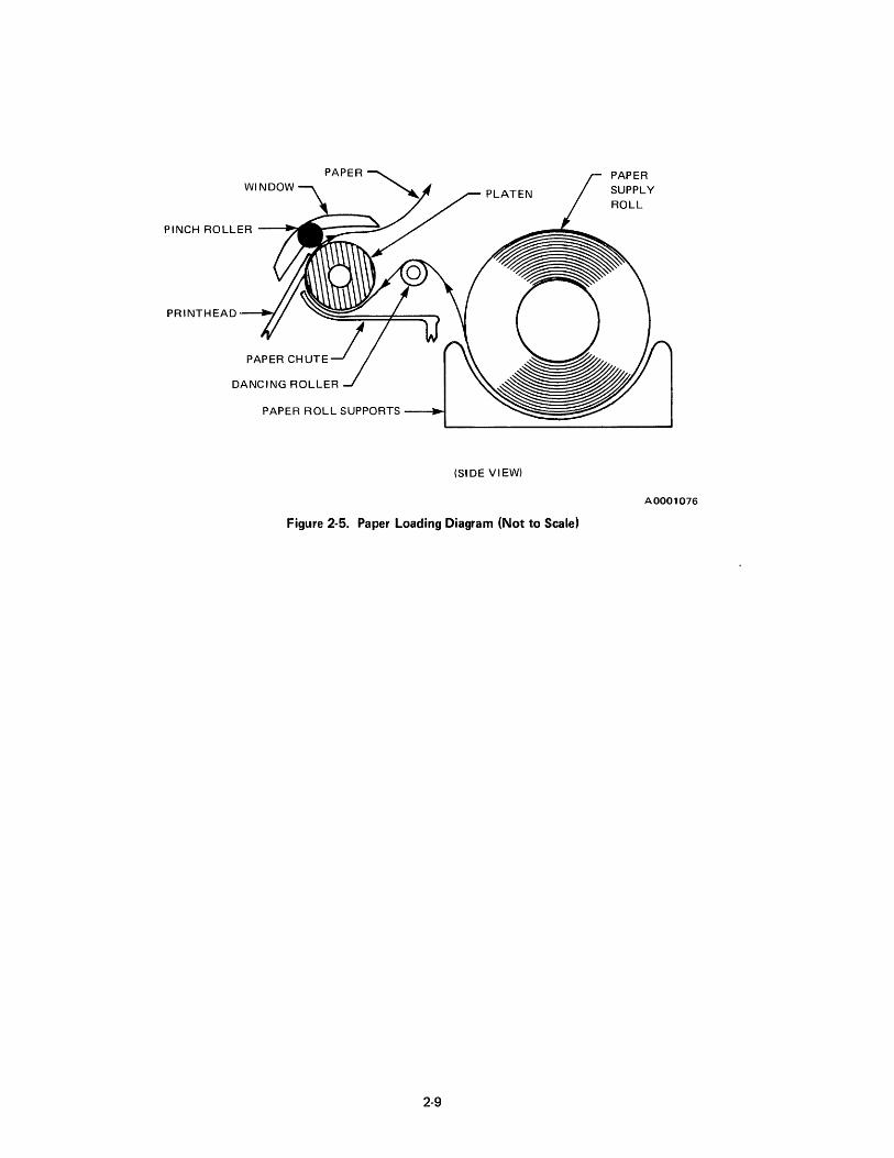
ROLL
PINCH ROLLER
PRINTHEAD
DANCING ROLLER
PAPER ROLL SUPPORTS
(SIDE VIEW)
A0001076
Figure 2-5. Paper Loading Diagram (Not to Scale)
2-9


SECTION 3
THEORY OF OPERATION
3.1 FUNCTIONAL DESCRIPTION. The Models 743/745 are low cost, light weight, interactive data terminals which utilize the thermal
printing technique. A functional block diagram of the
Models 743/745 is shown in Figure 3-1. The terminals
operate in two modes, 0 N- LI N E or 0 F F- LI N E, selecta ble by the operator.
•
•
ON-LINE Operation. With the terminal in
the ON LINE mode, the keyboard and printer operate in conjunction with the external interfaces as dictated by the
communications discipline and modified by the specific interface options.
OFF-LINE Operation. With the terminal in the OFF LINE mode, the terminal operates in a "typewriter" mode; i.e., the
keyboard is connected to the printer and
no aata is transmitted or received. All communications-related functions of the keyboard are inoperable in this mode (i.e., BREAK, HERE IS, etc.).
EIA
INTERFACE
.... ------, I I I OPTIONAL I
MECHANISM
DRIVE
ELECTRONICS
The following paragraphs in this Section describe the
theory of operation of the Models 743/745 Data Terminals. Schematics referred to in the text may be found in the appendix to this manual.
NOTE The Models 743/745 Data Terminals are supplied with one of two different paper handling mechanisms and one of two different electronics printed wiring
boards (PWB). The similarities and differences in these subassemblies are explained in the text where appropriate. Use the following table to determine which mech
anism and PWB your model has.
Terminal Serial No.
OX743YYYYY or OX745YYYYY
OX744YYYYY or OX746YYYYY
PRINTER
MECHANISM
Mechanism PWB
Part No. Part No.
983811 983841
999257 937300
COMMUNICATIONS
INTERFACE
CONNECTOR
I CHARACTER L-I SETS rI I CONTROL r---L ______ ..J
r-----' I OPTIONAL I II ANSWER-BACK !.--..
MEMORY ~
I (ABM) I I I L ______ .J
POWER
SUPPLY
ELECTRONICS ..... _____ T_AC_H_O_M_E_T_ER_S_EN_S_O_R ___ --'J--·t ... - ...
PRINTHEAD
DRIVE
ELECTRONICS
KEYBOARD
PRINTHEAD
Figure 3-1. Models 743/745 Simplified Block Diagram
3-1
.-----. I OPTIONAL I , ACOUSTIC I I COUPLER I I 'I ,MODEM, OR TTY I I INTERFACE I L _______ I
A0001077

3.2 CONTROL ELECTRONICS. The control electronics function in the Models 743/745 is performed by an interrupt driven, stored program, microprocessor system. The microprocessor system consists of a Texas Instruments TMS 8080 microprocessor, two 1 Kx8 TMS 4700 ROM's, (one 4Kx8 TMS 4732 ROM in the later models), a 64x8 TMS 4036 RAM, and a special purpose TMS 5504 I/O device.
The control electronics monitors all terminal inputs and generates all necessary timing and control signals to effect data transfers, cause printhead and paper motion, and generate printable characters through the thermal printhead matrix.
3.2.1 COMMUNICATIONS DISCIPLINE. The con· trol electronics monitors received data from the EIA or the optional interfaces. It generates the appropriate timing and code structure to transmit data entered through the keyboard. The control electronics transmits and receives asynchronous serial data in accord with ANSI Standard for Character Structure and Parity Sense X3. 16-1966 and ANSI Standard for Bit Sequence X3.15-1967.
3.2.2 SPEED (BAUD RATE). The terminal transmission speed is determined by an operator selectable, two-position rocker switch at 10 characters per second (110 baud) or 30 characters per second (300 baud).
3.2.3 BUFFERING. A buffer is provided to store characters received while a carriage return/line feed (CR/LF) is in progress. The combination of print time, CR time, and buffer is such that fill characters are not required and no data is lost even for an automatic CR/LF at column 81. This yields a true 3D-CPS printing capability (see paragraph 3.11.5 for details).
3.2.4 CHARACTER STRUCTURE. A character is made up of a start bit (always ZERO or spacing), seven data bits (least significant bit first), a parity bit, and two stop bits at 110 baud (always ONE or marking) or one stop bit at 300 baud (always ONE or marking). Figure 3-2 illustrates the character serial data timing. Tables 3-1 and 3-2 list the code structure for the ASCII, APL, and Katakana codes as interpreted by the term inal.
RKING I I I I I I I I
MA U.---l---l---l---l---l---l---l----] • I I I •• I • SPACING ___ .l ___ .J ___ .J ___ .J ___ .J ___ .l ___ .J __ _
BIT TIME ~
BIT TIME ~
*for 300 baud; 5.0
msec for 200 baud.
9.09 - DATA BITS msec A r ,
START B1 B2 B3 B4 B5 B6 B7 PARITY STOP STOP BIT (LSB) (MSB) BIT BIT BIT
~~----------------------CHARACTERTIME------------------------__ ~
100 msEl(.
a. 110 baud, 10 CPS Speed
3.33 ~ DATA BITS msec A
r , START B1 B2 B3 B4 B5 B6 B7 PARITY STOP
BIT (LSB) (MSB) BIT BIT
CHARACTER TIME ~1--------------------33.3 msec (300 baud) ----------------~
50 msec (200 baud)
b. 300 baud, 30 CPS Speed
Figure 3-2. Serial Data Timing Diagram
3-2
AOOOI078

Table 3-1. APL and ASCII Code System and Character Sets
CONTROL FOR BOTH
APL AND ASCII U. S. ASCII MODE APL MODE* ~~------------A-------------~v~------------~------------~
b7 0 0 0 0 1 1 1 1 0 0 1 1 1 1 bl> 0 0 1 1 0 0 1 1 1 1 0 0 1 1
b, 0 1 0 1 0 1 0 1 0 1 0 1 0 1
,b4 1\ '2 I[
0 0 0 ISPACE P ~~ QP ISV1\(;t: P ~
o 1 .~9,t:I, :.I?~ ><9 0 0 1 ! A Q 1 ex ? a q . o 0 0 STX DC 'il-
>c • )
1 [: ,>< ')
:)< )c
o 1 o 0 4 [. $ 4 D T .~ )( ~ 4 L - d t
1 [. ~e~ ": u
o 1 1 0 6 AC [:. ~.)( )'1<; ) -" -
o 1 1 1 7 fBEL / 7 G W :-: (i< ,)<''',,:>-
.. ~,« ] 7 V w g w
100 0 8 IBSl ( 8 H ')< < .~ 100 1 :-:HT ) y r; .Y~ 1\ 9 1 t i y
1 0 1 0 10 ILFI * : J Z > 'f" x =1= ( 0 C j z
101 1 11 ::: ::: J.~~ + K [
~ , ,
"-
1 1 0 0 12 .F.t:=. I:: , \ ~ ~J~ ,
1 1 o 1 13 ICRlt:· - ] y",>< m»< ~}~ + X I --+ m }
1 0 ~-::.$Q':: 1:- .x-
1 1 14 ::: . W~;0 . 1 1 1 1 15 k:.sl::: US a )c >< 5< b :L / \ DEL ; - x x
• APL characters are available only with the optional APL/ASCII keyboard.
D Pnntable characters
_ Printer control characters
AOO01400
Translated to uppercase equivalents by standard keyboard, or when UPPE R CASE ON L Y is selected on the optional Full-ASCII keyboard.
Codes generated and transm itted by the terminal, but no action is taken.
On standard (limited-ASCII) keyboard only: printed when received but not generated.
ASCII CONTROL CHARACTERS
(From USA Standards Institute Publication X3.4-1968)
ACK acknowledge EM end of medium NAK negative acknowledge
BEL bell ENG enquiry NUL null
BS backspace EaT end of transmission RS record separator
CAN cancel ESC escape SI shift in
CR carnage retu rn ETB end of transmission block SO shift out
DCl device control 1 ETX end of text SOH start of heading
DC2 device control 2 FF form feed STX start of text
DC3 device control 3 FS file separator SUB substitute
DC4 device control 4 (stop) GS group separator SYN synchronous idle
tDEL delete (also called RUBOUT) HT horizontal tabulation US unit separator
DLE data link escape LF line feed VT vertical tabulation
tnot strictly a control character
3-3

Table 3-2. Katakana and ASCII Code System and Character Set CONTROL FOR BOTH KANA & ASCII U.S. ASCII MODE KATAKANA MODE* r---~--~v~--------------~----------~v~------------~~------------~
b7 0 0 0 0 1 1 1 1 0 0 1 1 1 1 b6 0 0 1 1 0 0 1 1 1 1 0 0 1 1
bs 0 1 0 1 0 1 0 1 0 1 0 1 0 1
b4 b3 b2 b l No. 0 1 2 3 4 5 6 7 2 3 4 5 6 7
0 0 0 0 0 ~~U1: )?L_~:: SPACE 0 @ p ~» p SPACE , TA ~ MI
0 0 0 1 1 :_~O.tf j~~( ! 1 A Q A a- 0 i A 7- CHI A MU
0 0 1 0 2 ~ ~I}( ~ :))¢:t " 2 B R >Jl ><.F!: r 1 'J TSU j I I ME
0 0 1 1 3 J=I).{.: ~p.~~::~ # 3 C S >'C >CS M J ? U r TE .:f: MO
0 1 0 0 4 ~ ~Q.t~ ~9~.~.:~ $ 4 D T Q ~TM , .::r.. E ~ TO -y VA
0 1 0 1 5 ~~~.q~ :~~.~.: % 5 E U E >u . * 0 -t NA .:::L VU
0 1 1 0 6 ~f.~.: ~~.Y.~. ~ & 6 F V F >V 11 KA - 3 NI VO
0 1 1 1 7 BEL :.~:nf /
7 G W G' 'w 7 ~ .5( NU 7 A KI RA
1 0 0 0 8 IBS I :CAN: ( 8 H X :><HM ~ 1 I 7 KU * NE 9 RI
1 0 0 1 9 ::'HT:: ::::Efi::: ) 9 I . -.--.... ..... -....... Y x.1) )'! '? U 'T KE / NO )V RU
1 0 1 0 10 ILFI :.~~~~: * : J Z ~J M ">Z .:L E ::2 KO /\ HA V'RE
1 0 1 1 11 :::VT:: :::~.~G.:~ + ; K [ >cKy ~{? ;;f 0 -+j SA 1:. HI ORO
1 1 0 0 12 :::FF :: ::::'FS:::: , < L ¥VEN >L.: ~.~~ :;;'-.1:;;'-.y
VA ~ SHI 7 FU 9 WA
1 1 0 1 13 CR :::GS:::: M ] M ~}~ .::L A su "" HE ~ N VU
1 1 1 0 14 so :::RS:;: . > N /\ .~ %:~~ "3 ~ SE ~ HO " rnn
vo
1 1 1 1 15 :::US::: / ? 0 ~ :.P~L . 'J TSU 1 7 MA 0 ~:DEL: - SO .........
* Katakana characters available only with the optional Katakana keyboard.
D Printable characters
_ Printer control characters
AOOO1202
Codes generated and transmitted by the terminal, but no action taken.
Translated to uppercase equivalents when received by the terminal equipped with Katakana keyboard.
Printed when received, but not generated
IiII Ignored codes
ASCII CONTROL CHARACTERS (F rom USA Standards Institute Publ ication X3.4-l968)
ACK acknowledge EM end of medium NAK negative acknowledge BEL bell ENQ enquiry NUL null BS backspace EOT end of transmission RS record separator CAN cancel ESC escape SI shift in CR carnage retu rn ETB end of transmission block SO shift out OCl device control 1 ETX end of text SOH start of heading OC2 device control 2 FF form feed STX start of text OC3 device control 3 FS file separator SUB substitute OC4 device control 4 (stop) GS group separator SYN synchronous idle
tOEL delete (also called RUBOUT) HT horizontal tabulation US unit separator OLE data link escape LF line feed VT vertical tabulation
tnot strictly a control character
3-4

The standard Models 743/745 utilize a limited-ASCII character set. On the standard limited-ASCII keyboard, lowercase alphabet characters are not generated and are translated to their uppercase equivalents when received. Full-ASCII (lowercase capability), Katakana, and APL keyboards are available as options.
3.2.5 PARITY. The parity of received data is ignored by the printer. The parity of the transmitted character is factory-strappable between odd, even, or continous mark. Parity is not operator-selectable but is set at the factory according to the original purchase order. Even parity is supplied if not otherwise specified.
3.2.6 DUPLEX OPERATION. Duplex operation of the communications circuit is operator-selectable to either half- or full-duplex via the two-position HALF DUP switch on the keyboard. In full-duplex operation the terminal is capable of transmitting and receiving data simultaneously; any data typed on the keyboard is transmitted but not printed. In this mode it is possible to transmit data at the 30-CPS rate from the keyboard while the printer is simultaneously receiving data from the I ine at the 3D-CPS rate.
In half-duplex operation the terminal is capable of transmitting and receiving data, but not simultaneously. Any data typed on the keyboard is transmitted and also printed. In the Model 745 any data received from the line while the terminal is transmitting is ignored and is not printed.
3.2.7 ANSWE R-BACK MEMORY OPTION. The Answer-Back Memory option is implemented by a PROM inserted into a socket located on the printed wiring board (PWB) inside the Model 743/745 (see Section 3.10.8 for additional information).
3.2.8 KEYBOARD SCAN. The control electronics generates control signals to scan the keyboard and debounce keyswitch depressions. When a key depression is detected during a scan, the character is encoded and the appropriate action is taken by the terminal. Each scan is complete so as to detect possible multiple key depressions. When simultaneous depressions are detected during a scan, neither key is acted upon. This scanning/debounce technique effects a two-key rollover with lockout.
3-5
• 3.2.9 MECHANISM CONTROl. The control electronics also generates control signals for horizontal positioning of the printhead as well as vertical positioning of the printing paper.
3.2.9.1 Horizontal Printhead Positioning. The control electronics positions the printhead horizontally through the three-phase, 15-degree stepping motor. The motor is coupled mechanically to the printhead. The control electronics monitors an optical sensor mounted on the motor shaft which provides feedback to control both stepping motion during printing and slew motion during carriage return. The print/step cycle operates asynchronously up to 35 CPS during the period required to empty the data buffer.
Carriage return time for a full 80 columns is typically 180 milliseconds. A backspace consumes one character time. An automatic carriage return/line feed (CR/LF) is executed upon receipt from the keyboard or line of the 81st character in a line. Fault detection methods are used by the control electronics to prevent damage during power cycling conditions, obstruction of printhead motion, or loss of the optical sensor signal.
3.2.9.2 Paper Advance. The control electronics advances the printing paper by timing the current levels through the line feed stepping motor (or solenoid). The motor (or solenoid) is mechanically coupled to a ratchet mechanism which advances paper beneath the printhead. A line feed is performed in one charactertime. By holding the PAPER ADVance key depressed, the operator can direct the control electronics to perform repeated I ine feeds.
3.2.9.3 Printhead Pressure Control. The control electronics generates timed current levels through the printhead pressure solenoid which is mechanically coupled to the printhead pressure bar. Activating the solenoid relieves pressure upon the paper during line feed and carriage return operations; preserving line and character registration accuracy and reducing wear on the printhead.
3.2.9.4 Character Printing. Upon receipt of a character from the keyboard or the communications line, the control electronics generates the appropriate control signals to form the selected character utilizing the five by seven dot matrix on the thermal printhead. The print voltage is enabled, and then the matrix data is transferred to the printhead one column at a time.

3.3 PRINTER MECHANISM. The printer mechanism positions the printhead horizontally as each character is printed. The mechanism also returns the printhead to column one and advances the paper into position for the next line of print. The last character printed as well as the previous line are visible to the operator under normal lighting conditions. A line constitutes up to 80 character positions (columns).
The Models 743/745 employ either of two printer mechanisms. Horizontal printhead positioning and printhead pressure are implemented identically in both versions. However, one version uses a solenoid and ratchet arrangement to advance the paper (line feed); the second version uses a four-phase stepping motor for paper advance. The two types may be Identified as follows:
Terminal Serial No.
OX743YYYYYor OX745YYYYY
OX744YYYYYor OX746YYYYY
Mechanism & Electronics
Solenoid lIne feed mechanism (Part No. 983811) with PWB electronics (Part No. 983841) - Schematic 983842
Stepping motor line feed mechanism (Part No. 999257) with PWB electronics (Part No. 937300) - Schematic 937298
Printer mechanisms are supplied either with a printhead integral to the assembly (part number 983833 with solenoid line feed or 999257-0002 with motor line feed) or without a printhead (part number 983811 with solenoid line feed or 999257-0001 with motor line feed).
3.3.1 CHARACTER SPACING. Characters are spaced in 0.10D-inch increments (center to center) within a tolerance of ±0.005 inch.
3.3.2 LINE SPACING. Line spacing is 0.167 ±0.005 inch center to center, producing six lines per inch (single space).
3.3.3 PAPER SUPPLY. The mechanism accepts laD-foot rolls of paper with a 1.93-inch maximum outside diameter, wound with the heat-sensitive surface outside. The paper width is 8.54· inches maximum. The mechanism is designed to operate only with paper meeting TI Thermal Paper Specification 972603 and the TI Thermal Paper Print Quality Specifications 244156-9801, -9802, and -9803.
3-6
3.3.4 PAPER LOADING. After an initial line feed of at least 30 lines, paper will feed parallel between adjacent lines of print to within 0.02 inches, and all lines will be perpendicular to the paper edge within 0.05 inch.
3.3.5 PAPER TEAROFF. The back edge of the paper window is sharpened to provide means to tear off printed paper. This method minimizes paper waste and does not disturb the remaining paper supply.
3.4 PRINTHEAD SYSTEM. The printhead consists of a five by seven matrix of 35 heating elements and a transistor mounted on a monol ithic chip. Mounted on a heatsink, the chip is connected to the printhead interface PC card with a flexible cable. Mounted on the printhead interface PC card are two selected resistors (RTRIM and R3) which control the characteristics of the temperature compensation circuit so that its operation is optimum
for each individual printhead.
The printhead control electronics is identical for both PWB versions (TI part numbers 937300 and 983841). A block diagram of the printhead subsystem is shown in Figure 3-4.
Each of the 35 heating elements on the printhead consists of an SCR and a heating element. The 35
elements are controlled by the printhead driver address lines diagrammed in Figure 3-5. When both X and Y inputs are positive to a given element, the SCR energizes and remains on (approximately 10 msec) until PVOL TS is switched off.
3.4.1 PRINTHEAD DRIVERS. The printhead drivers are implemented on two SN98614 linear integrated circuits, each of which consists of six driver circuits. Each driver circuit has a low power, TTL, AND-input stage and a totem pole, power transistor output stage. All drivers are enabled by a signal called PHDSTRBE, and each is controlled by an individual (address) line from the processor.
Each driver translates TTL data into the levels necessary to control the printhead heating elements. The nominal output levels of the drivers are -4.7 volts low and +3.5 volts high.
3.4.2 TEMPERATURE COMPENSATION CIRCUIT. The printhead temperature compensation circuit provides a regulated, temperature compensated voltage to the printhead. The voltage is programmed by

OPAMPV103
(ON PRINTHEAD
INTERFACE PC CARD)
10 - 20% ENERGY TO PAPER
PRINTHEAD
TEMPERATURE
COMPENSATI NG
TRANSISTOR
(DT)
80 TO 90% ENERGY TO HEATSINK
CERAMIC HEATSINK
12 ROW/COLUMN
ROW/COLUMN DATA FROM
ADDRESS BUS (AO-All) AND PRINTHEAD
STROBE
A0001080
Figure 3-3. Model 7431745 Printing Subsystem Block Diagram
the selected resistors on the printhead interface PC card and the voltage drop across the base-to-emitter and collector junctions of the temperature compensation transistor on the monolithic printhead chip.
3.4.3 PRINT VOLTAGE CIRCUIT. Referring to schematic 937298, sheet 7 or 983842, sheet 6 in the appendix, Rl12 meters approximately 0.74mA of current to RTRIM and DT (temperature-compensating transistor). RTRIM and DT are connected in series with R 110 to ground on the printhead assembly. RTRIM is selected during manufacture so that its resistance compensates for variations in the voltage/ current characteristics of DT. Thus, the resulting PVOL TS is correct for a particular printhead. The resulting voltage at E 125 is nominally 0.964 volt.
When the PRINT signal is at logical ZERO from the processor, 0103 is energized, applying +5 volts to the cathode of CR 1 06 which holds it off and holds 0102 on. In the ON state 0102 has a maximum resistance of 60 ohms. At a 1-volt level RTRIM and DT have characteristic impedances of approximately 1.0V/0.75mA = 1.3k ohms. Capacitor Cl14 charges at a rate of (1.3k + O.06k) X 1 X 10⁻⁶ second or about a 1.4 msec time constant ±20% for variations in C114 and the voltage changes, and resulting imped-
'ance changes, in RTRIM and DT. The maximum charge time for Cl14 is 1.672 msec X 5 = 8.36 msec. The holding time for C114 is greater than 0.1 second with less than 1 percent drop.
3-7
When PRINT switches high and 0103 is off, the 0103 collector and CR 1 06 cathode are at -12 volts. This switches 0102 off and prevents the voltage on C114 from changing during a PRINT period.
Circuit gain is not changed when the CONTRAST potentiometer R 123 is adjusted. Gain is fixed at 70.
R122 is selected during manufacturing unit test of the PWB in order to calibrate the function of the temperature compensation circuit. This calibration enables use of any printhead with any PWB without any adjustment or circuit change.
CR 1 07 provides a level shift of 12 volts which enables amplifier Ul03 to output up to 22 volts and a minimum of 2 volts.
CR 108 and CR 1 05 provide two functions:
(1) Isolation of Q104 base from the gain loop of the compensation circuit which en
ables PVOLTS to be switched on and off without disturbing the circuit equilibrium
(2) The two diode drops shift the base potential of 0104 base position so that a dc measurement of PVOL TS can be made at the cathode of CR 1 07 without energizing PVOLTS.

MATRIX ADDRESS
YD7
YD6
YD5
YD4
YD3
YD2
YDl
XDl ___ ~
XD2 _____ ~
XD3 _______ ---'
XD4 __________ ~
XD5 -------_____ --l
__ --- PVOLTS
__ --- GND
C E
A0001081
Printhead Matrix Address Lines
NOTE
This view shows the printhead as it rests on the paper (from heatsink side of printhead), creating the letter "F".
PVOLTS --------------..... --------~ TO ALL ELEMENTS
TO OTHER SIX ELEMENTS
XDll --.... - ........ -----
1.2 K ohms
YDll---..... -~~Ar----~--~-~ 1.2 Kohms (PRINTHEAD ELEMENT)
90 ohms (HEATER ELEMENT)'
55 ohms
GND ----+---------------.... -------___ TO ALL ELEMENTS
~ ____ TO OTHER FOUR ELEMENTS
Printhead Element Block Diagram
A0001082
Figure 3-4. Printhead Matrix and Address Lines, and Printhead Element Block Diagram
3-8

0101 switches the base of 0104 to ground and holds it there except when PVOL TS is to be turned on. Diodes CR10l and CR102 provide base current to 0101 to keep it at ground whenever a break occurs in the DT/RTRIM circuit which would cause excessive PVOLTS.
As diagrammed in Figure 3-5, Cl13 and Rl08 control the initial step of PVOL TS and the rate of change of PVOL TS when 0104 is switched on by 0101 being turned off. 0103 and Cl09 form a timing circuit whose natural period is 10.5 to 15 msec. Normally, this circuit is switched on at the leading edge and off at the trailing edge of the 10-millisecond PRINT control signal from the processor. But only in case of a processor failure which allows PRINT to stay at a logic ONE level would the PRINT time be controlled by this circuit.
3.5 MECHANISM DRIVE ELECTRONICS The printer mechanism drive electmnics converts the processor control signals into the appropriate closedloop, controlled dc currents. The dc currents are applied to (1) a three-phase 15-degree printhead stepping motor, (2) a printhead pressure solenoid, and (3) to a four-phase stepping motor (on the 999257 mechanism) or to a solenoid (on the 983811 mechanism) for line feed.
The two printer mechanism versions and their associated PWB electronics may be identified as follows:
Terminal Serial No.
OX743YYYYY or OX745YYYYY
OX744YYYYYor OX746YYYYY
Mechanism & Electronics
Solenoid line feed mechanism 983811 with PWB electronics 983841 - Schematic 983842
Stepping motor line feed mechanism 999257 with PWB electronics 93730o-Schematic 937298
t T- t - +-1 ~ 1-1 ~ t ,
f r ; ~ - t t +-l- t t I ; t • +
-+--i ; ; t t-t
~ , , 1 t t
+ t .+
i , t- •
1- f
AOOO1OB3
Figure 3-5. Printhead Interface Timing (For Letter "F")
3-9

3.5.1 PRINTHEAD DRIVE MOTOR ELECTRONICS. The printhead positioning motor and electronics is identical for both mechanism versions (schematic 937298, sheet 7 or 983842, sheet 6). The electronics comprises four sections: phase-selecting circuits, a current decay time-constant circuit, and a feedback sensor circuit. A block diagram of the printhead drive electronics is shown in Figure 3-6.
3.5.1.1 Phase Selecting Circuits. Current in each of the three printhead drive motor phases is selected and controlled by three identical transistor networks:
Phase A - 0207, 0208, 0215 Phase 8 - 0206, 0204, 0202 Phase C - 0205,0201,0203
The operation of the circuits is discussed using only one network, phase A, as an example. The TTL logic level from U26-10 (PHA) selects current flowing in phase A. When this signal is a logic ONE, base current is supplied to 0207. Emitter current in 0207 energizes 0208, supplying sufficient base drive to saturate 0215. Emitter current of 0215 is applied to the phase A winding.
3.5.1.2 Current Regulator Circuit. Emitter current for 0205, 0206, and 0207 is controlled by the current regulator circuit. This circuit is a switching regulator type, synchronized to a 2D-kHz square wave signal (PWRCLK) from U28-8. The 2D-kHz signal is integrated by C203, R223, and C209: the resulting triangular signal is summed with the motor phase current sample voltage from R233 and is applied to pin 2 of U201. When the voltage at pin 3 of U201 is more positive than at pin 2, emitter current for the phase select circuits is switched on by U201 through R212. When the voltage at pin 2 is more positive, the emitter current is switched off.
The reference voltage at pin 3 of U201 is set by the processor to one of two levels, which consequently regulates the motor phase current to one of two levels. Hold current is regulated at 0.65 amps and step current is regulated at 1.4 amps. When the STEP signal from U26-5 is at a logic ZERO, the current regulator circuit applies hold current to the motor phase winding. When the STEP signal is at a logic ON E, step current is applied. As the STEP signal goes
SENSOR - .. -------------------------1 SENSOR FEEDBACK I
TO/FROM PROCESSOR
STEP
CIRCUIT
PHASE A IA
PHASE 7 PRINT-PHASE 8 18 HEAD SELECTING i DRIVE PHASE C CIRCUIT IC MOTOR -
I ........
CURRENT
DECAY TIME
CONSTANT CIRCUIT
CURRENT
REGULATOR IRETURN
CIRCUIT
1
1 A0001084
Figure 3-6. Printhead Stepping Motor Drive Circuit Block Diagram
3-10

from a logic ZERO to logic ONE, the current regulator circuit ramps the motor current up to 1.4 amps by charging C204 through R222 and R234 to prevent sudden changes in motor torque and to reduce audible noise in printhead movement.
3.5.1.3 Current Decay Circuit. When the current regulator senses sufficient current in the printhead stepping motor and switches off the current through 0215, the emitter of 0215 is suddenly switched from +30 volts to a negative voltage by the inductive flyback of the motor winding. The value of this negative voltage determines the time necessary to discharge the current in that winding. An approximation of this time may be computed using LI/V = t where
L = winding inductance I = motor current V = voltage from winding to ground t = time of current decay.
During periods when motor current needs to remain constant, transistors 0214 and 0209 are energized with base current via CR202 and R229. The flyback voltage during these periods is limited to:
VCR207 (-1 V) + VCE0209 (-1 V) or approximately -2 volts. This provides a very long discharge time and enhances regulator efficiency.
When the processor requires quick discharge of the phase current, it sets a logic ON E at the U26 pin 2, FAST signal. This energizes Q212 and 0213 which removes base current from 0214 and 0209. This enables VCE0209 to go to -22 volts, providing a 0.75 amps-per-msec discharge rate for motor winding inductance.
3.5.1.4 Feedback Sensor Circuit. The processor requires data on the position of the printhead stepping motor in order to "know" when to apply braking, to change phases, or to make other decisions concerning motion of the printhead carriage. This data is provided by the feedback sensor. Figure 3-7 diagrams the output characteristics of the feedback sensor circuit.
Primary operation of the feedback sensor is accomplished by a 24-position slotted wheel which interrupts a light path between an I R emitting diode and a photosensitive transitor. This assembly is mounted on the stepping motor which drives the printhead carriage. The circuit is shown in Figure 3-8 The current from the phototransistor is translated into a TTL logic level signal by the 02 and 03 circuit shown in Figure 3-9.
As the slotted wheel opens the light path, current flows through the phototransistor, energizing 02
r I 1 1 +-t-++- + f-f-f-' +- II i 1---1---1-- -t- -Tr-t I! -- t--H- : +-l-+--+--+-+-+-+-+--I!-t-\-+ - -+-+- -+-H ,- +-1--+--+-
1+-+-+-+--
1 -+~--+--+-- ,i--e--e-- -t- t--+- 1---1--- -1---1---1---
-+-+-+-+-+-+-+-' +t- H- -- -f-f-T + i+r-,_-L~--+ y-r-H- - r---,-- - - -- f-+- -1--+-1---
! -+-tt, I ,+- 1 L I I-I---t-t-t---+-+-' -:---t=+- -o:=:=,~r o~LL I or----r- j-It --' o'E ltf'~1 oT+- I 0'--1--- o-I---H-+--+--+-+-i +-1 i '++++ 6 -I-.-H- ~4 ~-++ -;-~ , r-t-- oO=+-_+~1+2 +4
0, +6
0 I J :+8 +10, -i-- +12 _I--- _+-+-+--+-+-+-_~
+-+-+ -1-+ -+--LLi--j- +-+-+-t--l- f-H---f--i--" I i -H- -t-+ -r- -+- a1=+-1 I-T+-I_+_+-+---+-+-+-+--I-+-+-+-+-_+-+-+-l-l I I I -l-~_+-+I 1-I-......... -+-+-4-+-+-I-+--+-f-+' -+1 .... + MOTION RIGHT +-11-1-+-', +-+-+-+-1-+-+-1--+-+--+-+1--+-+-+-+--+-1
+--+-1 L,EF r~ - -+--t-'i 't- 'f ! if +-+-" ttl , I, " 1 I --t-_ i .=1-+ I r ii' - , -+--+-+-+-1-+--+-+-+' -+-+-+--i -+-~- + +-t t 1 ' --;--r-r- +-+-+-+-1-++-+--+-+-+--+-++-1'-++-1
'+-+-+-+-+--+-+--+----I--I---l-+--H- ' ' . j' +-+-j' -I-- +--+-rl- f--+- I, + -+--+-+---+-+--1-++1t- -t-+-1+-~~Ti~i+-H-+, ! + ,--+- i::: ++-+-t i +--1-++--1-++--1,-++--1--1
Figure 3-7. Printhead Stepping Motor Drive Circuit Feedback Sensor Output Characteristics AOO01085
3-11

82 OHMS
LIGHT PATH BROKEN BY A 24-POSITION SLOTTED WHEEL
I ---4-+--_-~- ----_
SENSOR ASSEMBLY
P1 ,- - ----'---__ 4__+< SENS-I :
I I I I
3 , I ~---------------------+----------------------------+C GND
I I
1 I I ~---------------------------.----------------------------~ +5V I !... ____ I
A0001086
Figure 3-8. Printhead Stepping Motor Feedback Sensor Light Path Schematic
PWB ASSEMBLY +5V
J1 ,---I +n5V~ ______________________________ ~a-________ __
I I I I I I I
39K
R12 10K lK
03
TO FEEDBACKI SENS-I 4 ~----------~--~,~~--~--------~
SENSOR ....,
I I
~_G~ -5
10K
20K
AST2222 (2)
AOO01087
Figure 3-9. Printhead Stepping Motor Feedback Sensor Q2, Q3 Circuit Schematic
3-12

which deenergizes 03. Resistor R15 adds hysteresis to the circuit to provide regenerative feedback during transitions; this eliminates false triggering of the sensor.
3.5.2 PRINTHEAD PRESSURE AND LINE FEED CIRCUITS. The paper handling mechanism in the Models 743/745 uses one of two types of line feed drives. One version of the mechanism (TI Part No. 983811) incorporates two solenoids, one for paper line feed and one for printhead lift. The other version of the mechanism (TI Part No. 999257) has a solenoid-actuated printhead lift and a motor-driven paper advance (line feed). The following discussion distinguishes between the two types of mechanisms, first describing the two-solenoid mechanism and then the motor/solenoid arrangement.
Refer to schematic 983842, sheet 6 for the solenoid/
solenoid mechanis~; and to schematic 937298, sheet 7 for the motor/solenoid drive.
3.5.2.1 Solenoid/Solenoid Drive (983811). Both solenoid drivers basically are transistor voltage switches which provide a means for the processor to energize the two solenoids (one for printhead pressure and one for line feed). The transistors are NPN Darlington devices with a minimum current gain of 1000. Base current is provided when the processor sets U25, pin 15 for line feed and U25, pin 5 for printhead lift to a logic ONE. The collector of 0251 saturates +1.5 volts (maximum) sinking current for the line feed solenoid. When the processor resets U25, pin 15 to a logic ZERO, 0251 goes off; simultaneously, the inductive flyback of the solenoid current drives the collector of 0251 to a peak of approximately +65 volts. During the flyback, current flows through CR251 and R257, discharging the inductive current from the solenoid.
The printhead lift circuit is similar to the line feed except that the +30 volts is applied to the junction of R258 and CR252. This limits the current in the printhead pressure solenoid to a maximum 0.9 amps and limits the voltage stress on 0252 to about +31 volts.
3.5.2.2 Motor/Solenoid Drive (999257). The drivers are saturated transistor voltage switches controlled from the processor buffer for energizing the LF-step B-printhead lift solenoid and/or the LF-step A-line feed stepping motor. The transistors are NPN Darlington devices with a minimum current gain of 1000 specified for inductive switching applications.
3-13
a.
b.
Step No.
1A 18 2A 28 3A 38 4A 48
Printhead Lift Without Line Feed. The printhead lift function i$ performeq when the base drive resistor R 253 for 0251 and the base drive resistor R 255 for 0252 are switched to a logic ONE level. This turns on 0251 and 0252, causing current flow from +30 through fuse F252 and the printhead lift solenoid and parallel resistor R 258 through both sets of motor windings through 0251 and 0252 to the 30 V supply return. The transistors inductively clamp the stored inductive energy
upon turn-off. The printhead-liftwithout-line-feed function is subject to a maximum 20 percent duty cycle, based on a maximum on-time of 45 seconds.
Printhead Lift With Line Feed. The processor performs a printhead-lift-with-line
feed by switching the base drive resistors R253 for 0251 and the base drive resistor R255 for 0252 to a logic ONE level in the following sequence:
Transistor Phase
Motor Phase Time ON
(degrees) ON (msec)
0251 7.5 0-3 0251 15.0 2 3-6 0252 22.5 3 6-9 0252 30.0 4 9-12 0251 37.5 12-15 0251 45.0 2 15-18 0252 52.5, 3 18-21 0252 60.01 4 21-24
Motor-phase 1 is energi zed by the charging of capacitor C213 from +30 V through the motor winding, and returns through 0251. Motor-phase 2 is dccoupled and is energized when 0251 is turned on. Motor-phase 3 is energized by the charging of capacitor C212 from +30 V through the motor winding and returns through Q252. Motor-phase 4 is dc-coupled and is energized when 0252 is turned on. Diodes CR251 and CR252 provide reverse-voltage protection for capacitors C213 and C212. Printheadlift-with-line-feed is subject to a maximum duty cycle of 40 percent, based on a maximum continuous line feed of 330 seconds.

3.6 KEYBOARDS The standard keyboard for the Models 743 and 745 is a limited-ASCII (uppercase alphabet characters only) version with an integral numeric keypad for fast number entry.
An optional, full-ASCII keyboard is capable of generating/printing both lowercase and uppercase alphabet characters. Table 3-1 shows the code structure of the ASCII code as interpreted by the standard and full-ASCII keyboards.
An optional APL/ASCII keyboard generates/prints the special programming characters shown in Table 3-1 in addition to the full-ASCII character set.
An optional Katakana keyboard generates/prints the Katakana characters and limited-ASCII characters shown in Table 3-2.
All keyboards are TTY33-compatible, alphanumeric devices equipped with a carrier detect lamp which indicates that the data carrier is being received (or that the carrier detect signal is biased ON).
The dot pattern structure of the various character sets is illustrated in Figures 3-10 and 3-11.
The following special-function keys are provided on all keyboard versions:
a. PAPER ADVance - When held depressed, the PAPER ADV key causes the printer to perform a carriage return (CR), and continuous line feeds (LF) after returning the printhead to column one; no code is transmitted. A 200-millisecond pause follows the first line feed before continuous line feeds are performed.
b.
c.
d.
BREAK - The BREAK key, when depressed, causes the terminal to transmit a continuous space as long as the key is depressed and the terminal is on-line.
HERE IS - The HERE IS key, when depressed, causes the optional answerback memory contents (if installed) to be transmitted if the terminal is ON-LINE.
REPT - The REPT key, when held depressed in addition to a character key, causes the terminal to repeatedly generate the character at the terminal operating
3-14
e.
f.
g.
speed. (This key is not provided on the APL keyboard, which has an automatic repeat feature.)
LOW SPEED - The LOW SPEED control is a two-position rocker switch which sets the transmission rate to 10 characters per second (CPS) when pressed to the left or 30 CPS when pressed to the right.
HALF DUPlex - The HALF DUP control is a two-position rocker switch which sets the communication status to half duplex when pressed to the left or full duplex when pressed to the right.
ON LINE - The ON LINE control is a two-position rocker switch which sets the terminal to on-line status when pressed to the left or local status (off line) when pressed to the right.
3.6.1 STANDARD KEYBOARD. The standard keyboard is equipped with 54 single action keys, four two-position rocker switches, and one carrier detect indicator lamp. The integral numeric keypad is activated by pressing the NUM rocker switch to the left; then only the "shadow box" keys are enabled.
Standard keyboard layout and symbolization are shown in Figure 3-12. The output status when the CTR L (control), NUM (numeric), and SH 1FT controls are not activated is shown in Figure 3-13. Figures 3-14, 3-15, and 3-16 illustrate, respectively, the output status of the various keys when the SHIFT, CTRL, and NUM controls are activated.
NOTE Some models of the standard keyboard are equipped with alternate-action lOW SPEED, HALF DUP, ON LINE, and NUM keys instead of rocker switches.
3.6.2 OPTIONAL FULL-ASCII KEYBOARD. The optional full-ASCII keyboard is equipped with 59 single-action keys, four two-position rocker switches, and one carrier detect indicator lamp.
Full-ASCII keyboard layout and symbolization are shown in Figure 3-17. The output status when the CTR L (control) and SH I FT keys are not depressed is
shown in Figure 3-18. Figures 3-19 and 3-20 depict, respectively, the keyboard output when the SHtFT and CTRl keys are activated.

U. S. ASCII MODE \ APL MODE
A
" , , , ,
b, II 0 0 1 1 1 \\0 0 1 1 1 1
b6 II 1 1 0 0 1 1 1 1 0 0 1 1
bs----" 0 1 0 1 0 1 0 1 0 1 0 1
~ b3 b2 bl 2 3 4 5 6 7 I 2 3 4 5 6 7
mm II I I I I I II I I I I 000 0 SPACE
t±±l±l BLANK 0 NEG SIGN STAR DIAMOND P
000 1 I I I I I I I I Ii I I I DIERESIS 1 ALPHA QUERY A Q
001 0 I I I I I I I I I I I I R PARENTH 2 DECODE RHO B R
001 1 I I I I I I I I I I I I LESS THAN 3 INTERSECTION CEILING C S
o 1 0 0 I I I I I I I I I I I I LESS OR EQUAL 4 FLOOR LOGIC NOT D T
o 1 0 1 I I I I I I I I I I I I !'QUAL 5 EPSILON DROP E U
o 1 1 0 I I I I I I I I I I I I GREATER THAN 6 UNDERSCORE UNION F V
011 1 I I I II I I I I I I I I RT BRACKET 7 DEL OMEGA G W
1 000 I I I I I I I I I I I I OR 8 DELTA REV IMPLICATION H X
1 0 0 1 I I I Ii I I I I I I I I AND 9 IOTA TAKE I Y
101 0 I I I I I .-. I I I I I NOT EQUAL LFT PARENTH NUL IMPLICATION J Z
1 0 1 1 I I I] I I I I I I I I I DIVIDE LFT BRACKET QUOTE LFT_ ARROW K LFT BRACE
1 100 I I I I I I I I III I I I COMMA SEMI-COLON QUAD LFT TACK L RT TACK
1 101 I I 11 I I (I I I I I I I PLUS TIMES MODULUS RT. ARROW M RT BRACE
1 1 1 0 I I • I I I I I I I I I PERIOD COLON ENCODE GREATER OR EQUAL N ooLLAR SIGN
1 1 I I III I I ~ I I I I I ~ 1 1 DELETE DELETE
t±±l±l t:tl±tJ SLASH BACK SLASH CIRCLE MINUS 0
NOTE: Lowercase characters are translated and printed as uppercase characters by the standard limited-ASCII keyboard.
AOOO1393
Figure 3-10. APL and ASCII Character Set Generation
3-15

u.s. ASCII MODE KAT AKANA MODE I
( J. 'r ___ -----J. ------.
b~ .. 0 0 1 1 1 1 0 0 1 1 bh .. 1 1 0 0 1 1 1 1 0 0
Bits b, - 0 1 0 1 0 1 0 1 0 1
o 0 0 0 I I I I I I ; I ITA IMI o 0 0 1 I III I I I I I It ILIMU o 0 1 0 I I I I I I I I, ITSUIME o 0 1 1 I I I I I I I Iu ITE IMO o 1 00 I I I I I I I IE ITO IVA o 1 0 1 I I I I I I I 10 ilL Ivu o 1 1 0 I I I I I I I ilL INI Iva o 1 1 1 I I I II I II IA IKI It IRA 1 0 0 0 I I III I III I I, IKU IJIt. 1 0 0 1 I I I ., I ., Iu IL INa IRU 1 0 1 0 I I I I I I IE IKo IHA It 1 0 1 1 I I I I I I] 10 ISA IHI IRa 1 1 0 0 I I] I IVENI I IVA It,IFU IWA 1 1 0 1 I I II I II I Ivu Isu It IN 1 1 1 0 I I II I II I Iva ISE IL 19 11111111111TSUIsoiMAI
AOOO1203
- Figure 3-11. Katakana and ASCII Character Set Generation
3-16

NUMED SPACE 0 I
• ON ED CARRIER DETECT LINE INDICATOR
A0001196
Figure 3-12. Standard Limited-ASCII Keyboard Layout and Symbolization
ED SI"ACE • ON ED LINE
A0001197
Figure 3-13. Codes Generated with no Mode Keys Activated (Standard Keyboard)
[J[J~Dc:Jc:JDDDDLJCJ~ El BDDDDDDDD[J~~. B DDDDDDD[]D~IE!lIl~rn
.DDDDDCJDODc] ED SI"ACE
A0001198
NOTES, D A blank key indicates that a NUL code is •• ansmitted.
HALF ED DUP
• ON ED LINE
Figure 3-14. Codes Generated with the SHIFT Key Pressed and Held (Standard Keyboard)
3-17

rn SI"ACE • AOOOl199
NOTE : D A blank key indicates that a NU L code is transmitted.
The CTRL (Control) key overrides the SHIFT key.
t=I I::J
B LOW rn
SPEED
HALFrn DUP
ON rn LINE
Figure 3-15. Codes Generated with the CTR L Key Pressed and Held (Standard Keyboard)
DDDDDD~~~DDD~ DDDDDDD[]~EJD§]III
DDDDDDEJ[][]DDIl DDDDDD~[][JD
NUMrn • A0001200
NOTE, D A blank key indica.es that a NUL code i ..... smitted.
The NUM (Numbers) switch overrides the SHIFT and CTRL keys.
Figure 3-16. Codes Generated with the NUM Switch Set (Standard Keyboard)
t=I I.:::J
B LOW rn
SPEED
HALFrn DUP
ON rn LINE
m~mmmrnrTlmrnr:::lfGslRrnr.;;lD UJWWWW6L.ZJL§J9LQ.JL::...J~~L!J(ID
CJ1~~~~~~~[H!l~fDiElf!.ULlrnrnDIl t:lJ L9J (j!J W LBJ L!.J W U!J W l..Qj L.fJ ~ [ ] L:J
1I~~~~fBiLlm~~mrnrTl~~r,;;;] lAJ W L.Q.J L.fJ L§J L.!:!..J W W W ; Li.J ~ l::J I.!:J
• ~ r!J rm ~ [AJ lID [MJ EJ LJ ~ LOW rTI SPE ED L...Ii....I
UPPE R rT"""t CASE ~
AOOOl192
SPAC E HALF r-r-1 ON ~ DUP L..J....J LINE I..J..J • (Carrier Detect Indicatorl
Figure 3-17. Optional Full·ASCII Keyboard Layout and Symbolization
3-18

UPPER rr""'1 CASE ~
A0001193
CD A0001194
SltAC E
NOTE: If UPPER CASE is not selected, a to z are printed in lowercase If UPPER CASE is selected, A to Z are printed in UPPERCASE
LOW r-r-1 SPEEOL-'-'
HAlF,-..,....., ON CD OUP L...J...J LINE • (Carner Detect Indtcatorl
Figure 3-18. Codes Generated with no Mode Keys Activated (Full-ASCII Keyboard)
SltAC E
NOTE: The SHIFT key overrides the UPPER CASE switch -~
LOW rn SPEEDL-'-'
HAlF,-..,....., ON CD DUP L..L...J LINE •
Figure 3-19. Codes Generated with the SHIFT Key Pressed and Held (Full-ASCII Keyboard)
DDDDDDDDDDLJDD§8 ElEJEJLJEJEJLJEJLJLJLJCJDDEJIl IILJEJLlEJLJLJLJLJLJDD~§§
EJElLJEJLJLJLJ[J[j[J LOW rn SPEEDL.L.J
rn SPAC E HALF r"T"'"l ON CD DUP L...L...J LINE
AOOO1195 • NOTE : D A blank key indicates that a NU L code is transmitted.
The CTRL (Control) key ov..ndes the SHIFT key and UPPER CASE Switch.
Fiwure 3-20. Codes Generated with the CTRL Key Pressed and Held (Full-ASCII Kevboard)
--3-19

NOTE When the UPPER CASE rocker switch is activated, only uppercase al phabet characters are generated/printed.
3.6.3 OPTIONAL RECEIVE-ONLY CONTROL PANEL. The Models 743 and 745 Receive-Only Data Terminals are equipped with a control panel in place of a keyboard. The control panel shown in Figure 3-21 has PAPER ADVance and LOW SPEED controls and a carrier detect indicator, all of which function the same as on the keyboard models. Limited-ASCII and full-ASCII versions are available, as well as Answer-Back Memory (ABM). A programmable ROM is used to implement the ABM.
3.6.4 OPTIONAL APL/ASCII KEYBOARD. The optional APL/ ASCII keyboard is equipped with 59 single action keys, four two-position rocker switches,
A0001272
and one carrier detect indicator lamp. Table 3-1 shows the code structure of the ASCII and APL codes as interpretd by the keyboard.
The APL rocker switch on the left front corner of the
keyboard permits selection of either the ASCII mode or the APL mode. APL/ASCII keyboard layout and symbolization are shown in Figure 3-22. With the APL rocker switch depressed to the left (APL position), the terminal operates in the APL mode. The output status in the APL mode is shown in Figure 3-23 with no mode key depressed and Figure 3-24 with the SHI FT key depressed.
With the APL rocker switch depressed to the right, the term inal operates in the ASC II mode. The output status in the ASCII mode is shown in Figure 3-25 with no mode keys depressed and Figure 3-26 with the SH I FT key depressed.
PAPER ADV
LOW SPEED
CD
• (CARRIER DETECT INDICATOR)
Figure 3-21. Optional Receive - Only Control Panel (Replaces the Keyboard).
APL l=f3 KEYTOP LEGEND
.. ~APl SHIFTED CHARACTER
i .. I\1 APl UNSHIFTED CHARACTER
!~ASCII SHIFTED CHARACTER
-~ASCII UNSHIFTED CHARACTER
HALF r-r-l OUP i:::::±:::l
80001392 Figure 3-22. Optional APL Keyboard Layout and Symbolization
3-20
l?:E~ • (Carrier Detect Indicatod

A0001395 NOTE: Upperc:ase-only status is ignored in APL mode.
ON r--1'--1 LINE I:::::±::::]
• Figure 3-23. Codes Generated in the APL Mode with no Mode Keys Activated (APL Keyboard).
s~~1=f1 I~----~--------
APL I=f1 HALF r-T'""l DLF~ L?:~
A0001396 • NOTE: Uppercase-only status is ignored in APL mode.
Figure 3-24. Codes Generated in the APL Mode with the SHIFT Key Pressed and Held (APL Keyboard).
A0001397
I~----~--------HA LF r-T'""l DLF~
NOTE: If UppercasH)nly is enabled (CTRL, SHI FT, g A to Z are printed in IJPI*C-. If uppen:ase-onIy is not .... bIed, A to Z are printed in I~
~~~ L':~
•
Figure 3-25. Codes Genented in the ASCII Mode with no Mode Keys Activ .... (APL Keyboa-d).
3-21
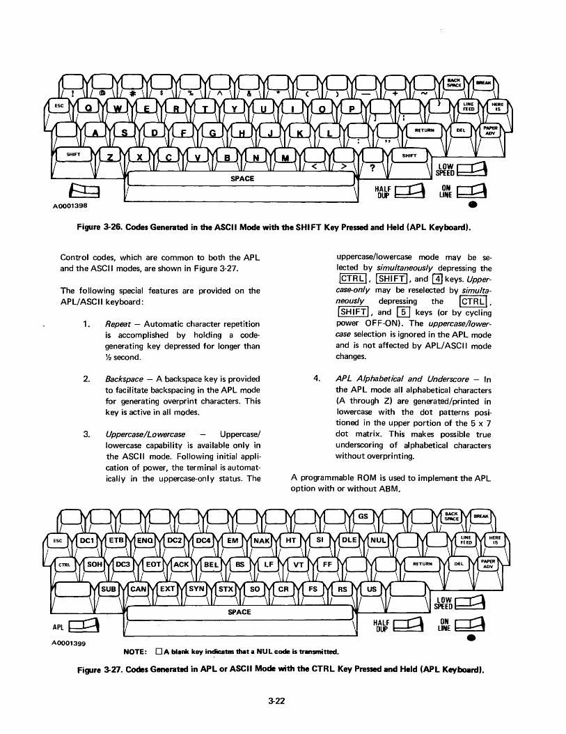
AOO01398
ON r-T""""\ LINE I:::::::!:::::J
• Figure 3-26. Codes Generated in the ASCII Mode with the SHI FT Key Pressed and Held (APl Keyboard).
Control codes, which are common to both the APL and the ASCII modes, are shown in Figure 3-27.
The following special features are provided on the APL/ASCII keyboard:
1. Repeat - Automatic character repetition is accomplished by holding a codegenerating key depressed for longer than % second.
2.
3.
AOO01399
Backspace - A backspace key is provided to facilitate backspacing in the APL mode for generating overprint characters. This key is active in all modes.
Uppercase/Lowercase Uppercase/ lowercase capability is available only in the ASCII mode. Following initial application of power, the terminal is automatically in the uppercase-only status. The
4.
uppercase/lowercase mode may be selected by simultaneously depressing the ICTR L I, I SH I FT I, and @] keys. Upper
case-only may be reselected by simultaneously depressing the I CTR L ( , ISHIFT/, and []J keys (or by cycling power OFF-ON). The uppercase/lowercase selection is ignored in the APL mode and is not affected by AP L/ ASC II mode changes.
APL Alphabetical and Underscore - In the APL mode all alphabetical characters (A through Z) are generated/printed in lowercase with the dot patterns positioned in the upper portion of the 5 x 7 dot matrix. This makes possible true underscoring of alphabetical characters without overprinting.
A programmable ROM is used to implement the APL option with or without ABM.
ON r-T""""\ LINE I:::::::!:::::J
• NOTE: 0 A blank key indicates that a NU L code is transmitted.
Figure 3-27. Codes Generated in APl or ASCII Mode with the CTRl Key Pressed and Held (APl Keyboard).
3-22

3.6.5 KATAKANA KEYBOARD. The optional katakana keyboard shown in Figure 3-28 enables the terminal to transmit/receive both standard U.S. ASCII characters and katakana characters. Two special keys are provided: the KANA mode key permits generating/printing the characters shown in Figure 3-29 and 3-30. The ALPHA mode key permits generating/printing the characters shown in Figures 3-31 and 3-32. The control codes shown in Figure 3-33 are generated when the CTR L key is depressed.
The following actions occur when the keyboard is set to the Kana or Alpha (ASCII) mode:
a. In the ALPHA MODE (Alpha mode indicator ON) when ON LINE and in FULL DUPLEX: (1) Pressing the Alpha Mode key causes the
terminal to transmit the SI (shift in) code.
b.
(2) Pressing the Kana Mode key causes the following: • Keyboard enters the Kana mode. • Terminal transmits the SO (shift
out) code. (3) When the terminal receives SI (shift in)
from the line, the printer enters the Alpha mode.
(4) When the terminal receives SO (shift out) from the line, the printer enters the Kana mode.
In the KANA MODE (Alpha mode indicator OFF) when ON LINE and in FULL DUPLEX: (1) Pressing the Kana Mode key causes the
terminal to transmit the SO (shift out) code.
(SPACE)
KEYTOP LEGEND.
uS ASCII / ,SHIFTED lOR ~
" CTRLI US / ASCII ~ KANA
~:;HIF ~x ,SHIFTED
c.
d.
e.
(2) Pressing the Alpha Mode key causes the following: • Keyboard enters the Alpha mode • Terminal transmits the SI (shift
in) code. (3) When the terminal receives SO (shift out)
from the line, the printer enters the Kana mode.
(4) When the terminal receives SI (shift in) from the line, the printer enters the Alpha mode.
In the on-line and half-duplex mode (the ON LINE and HALF DUP switches to the left) the ALPHA and KANA modes of both keyboard and pri nter can be changed from the keyboard. The printer mode also can be changed by received data.
I n the on-line. and full-duplex mode (the ON LINE switch to the left and the HALF DUP switch to the right) the ALPHA and KANA mode keys affect only the keyboard mode. The printer mode can be changed only by the SI or SO codes in received data (from the host computer). The keyboard and printer modes are independent of each other; the keyboard could be in the alpha mode while the printer is in the Kana mode. The keyboard alpha mode indicator lamp indicates only the keyboard mode.
Upon power-up or after pressing the RETURN key to clear a paper-out or printeheacl jam condition, both the keyboard and the printer will be initialized to the ASCII alpha mode.
NOTES
HALF r-I1'l LOW r-Il'l ON r-TI'l DUP ~ SPEEDL....l...U lINEL.l....dJ
~ L-CARRIER
DETECT INDICATOR
UN:':;~~E~ " " 1. 2.
The Alpha Mode Indicator is ON for the Keyboard Alpha Mode and OFF for Keyboard Kana Mode. AlpM Mode (SI) and Kana Mode (SO) ch.-.cws cannot be ......... lIIiIII ... REPT key.
AOO01201 Figure ~28. Optional Katakana KeybcNwd Layout and Symbolization
3-23

w[JGJGJGJGJGJGJGJGJGJDOrrlEl ElwGJ[JCJGJ[JGJ[JGJGJDDE1E1~ o~GJ[JCJCJGJ[JGJDQ[JGJ[J[§]a BGJGJGJ[J[JOGJGJCJGJGJ6@!) ~ I (SPACE) I HALF r-rI') LOW r-rI') ON IT!) ~ DUP L...I...JJ SPEED\.....l..JJ L1NE~
AOO01204 Figure 3-29. Katakana Keyboard Codes Generated in the Unshifted Kana Mode (Alpha Mode Indicator OFF)
DDD[3GD[3[3DDDDD~El ElDDDDDDDDDDDDE1E1~ o~~: DDDDDDDDDDDDl§18 6[3DDDDDDDGDD6@!) ~ I (SPACE) I HALF r-rI') LOW [[] ON IT!) ~ DUP L...I...JJ SPEED LINE ~
AOOO1207 Figure 3-30. Katakana Keyboard Codes Generated in the Kana Mode with the SHIFT Key Pressed and Held . (Alpha Mode I ndicator OF F)
EJ[JElEJDEJDEJDEJDDD~El ElEJEJDEJDDDDEJDDDE1E1~ o~~: ElDEJDDEJEJDDDDDDB DEJEJDE1DEJEJDDD DD@!) D I (SPACE} I H~~ [[] .}:'~[[] LI~~ cp
AOOO1205 Fi.,re 3-31. Katllkana Keyboard Codes Generated in the Unshifted Alpha Mode
(Alpha Mode Indicator ON)
3-24

DDCJCJCJCJDDCJDCJDO[y]E1 E]DDDDDDDDDDDDEl8~ o~~: DDDDDDDDDCJDDDEl BDDDDDDDCJCJCJLJa~ ~ I (SPACE) I HALF []] LOW []] ON IT\) ~ • DUP SPEED LlNE~
o AOOO1206
Figure 3-32. Katakana Keyboard Codes Generated in the Alpha Mode with the SHI FT Key Pressed and Held (Alpha Mode Indicator ON)
DDDDDDDDDDDBB[y]E1
(SPACE) HALF []] LOW []] DUP SPEED
ON IT\) LlNE~
o NOTE: The CTRL (Controll key overrides the SHIFT key in both Kana and U.S. Mod ..
AOOO1208
Figure 3-33. Katakana Keyboard Control Codes Generated with the CTR L (Control) Key Pressed and Held
3.7 OPERATOR CONTROLS AND INDICATORS.
Operator controls and indicators in addition to those contained on the keyboard include the following:
a.
b.
Power Switch - a toggle switch is used to switch both sides of ac line power to the terminal. The switch is located on the top right rear corner of the case.
Bell - a buzzer is provided to produce an audible signal which has a frequency of 3.2 kHz nominaL Duration of the signal is 250 ±25 milliseconds for reception of the ASCII BEL character from the line or local.
3-25
3.8 POWER SUPPLY. The Models 743/745 power supply (see schematic 983842, sheets 1 and 2 or 937298, sheets 1 and 2) converts ac input power to the regulated dc output power required to drive all circuits within the terminal. The output is listed in Table 3-3. The power supply is designed to operate without degraded performance over the full range of steady-state and transient conditions. The Models 743/745 Terminals consume a maximum 75 watts.
The power supply is a multiple output, self-oscillating converter/regulator. The ac input is rectified and filtered in the unregulated supply, converted to regulated pulsating voltage in the converter, and rectified and filtered in the output to provide the

Table 3-3. Power Supply dc Outputs
Percent Output Output Regulation Voltage Current with Transient
(VcIe) ( amps) Line/Load and Offset
+30 1.8 ±10% +12 .25 ± 5% -12 .40 ±10% + 5 .80 ± 5% - 5 .15 ± 5%
appropriate regulated voltages to the load. A block diagram of the power supply is shown in Figure 3-34. A single ferrite core transformer provides drive to the power switch transistor, multiple output voltages, input-output isolation, and output voltage regulation. The power supply operates in the flyback mode; that is, energy stored in the transformer is delivered to the load(s) during the off time of the power transistor. Thus, only a single power transistor is necessary. The required base drive power at the optimum impedance level is provided directly from the transformer.
Input ac power, after passing through a high frequency noise filter (T302-C325-C326), is rectified by diode bridge CR323-326. The resulting dc current then passes through R330 and SCR0310 (normally on) where it is smoothed before storage across filter capacitors C306 and C308, from which the input or primCf"Y side dc current is supplied.
3.8.1 POWER TRANSFORMER. The power supply circuit is self-oscillating; the positive feedback path passes from the power transformer primary (terminals
ACIN UNREGULATED
SUPPLY ~
I ~
SOFT ~
START ,-
y '--
I
1 and 2) to the base-drive winding (terminals 13 and 14). The base drive signal is coupled through C318 and diode CR315, then through current-setting resistor R322 to the base of power transistor 0311. Oscillation begins when the primary-side dc appears. A current set by R329 and R324 flows through R322 into the base of 0311, bia~ing it to approximately 50 to 100 rnA collector current. Random noise components of the 0311 collector current thus ensures that its collector current will increase because of the positive feedback from primary to base windings. The base current established through R322 ensures that 0311 will saturate. Therefore, the collector current of 0311 will increase linearly as determined by the primary inductance of transformer T301 and the input dc supply voltage impressed across it.
When the voltage drpp across R338 produced by the 0311 emitter current has risen to' approximately 0.6 volt, 0309 begins to conduct, shunting base drive from the power transistor base which causes it to lose saturation. As soon as its collector voltage begins to rise, 0311 is rapidly switched off by regenerative feedback. Falling collector current causes rising collector voltage (because of the transformer primary inductance), resulting in falling base drive voltage and fall ing base current. The collector voltage of 0311 "flys back" above the input dc supply voltage (resulting in reverse base drive current coupled through C318) until the rectifier(s) in the transformer secondary circuit(s) become forward biased, and currents flow into the output filter capacitors (and output load resistances). The energy stored in the magnetic field of the transformer during the "on"
OUTPUT RECTIFIERS
CONVERTER AND ~ DC OUT
~ FILTERS
r--
VOLTAGE I-REGULATOR
FAILURE r--PROTECT
Figure 3-34. Model 743/745 Power Supply Functional Block Diagram AOOO1114
3-26

time of 0311 is transferred to the output during the "off" time of 0311.
A 3O-volt output is obtained from winding 3-4, rectified by CR322, and filtered by C332 and C331. Positive and negative 12 volts are obtained, respectively, from windings 9-10 and 11-12, diodes CR301 and CR304, and capacitors C301 and C303. Positive 5 volts is obtained from winding 7-8, rectified by CR302 and CR303 in series, and filtered by C302. The higher drop of the series-connected diodes permits obtaining 5 and 12 volts from input flyback voltages with a 2 to 1 ratio (about 6.35 and 12.7 volts).
Secondary current(s) continue to flow, decreasing (approximately) linearly with time, until the transformer flux has fallen essentially to zero. The transformer terminal voltages remain at their flyback values during the entire period of secondary current flow. During a single flyback period the output voltages rise only a few percent of their full values, as determined by the output capacitors. As the flyback currents fall to zero, the voltages across the transformer windings decay toward zero. During the fly back interval C318 acquires a charge of about 1 volt (left hand side positive) from current drawn from R322 which is clamped by 0309. Transistor 0309 acts as an emitter follower in the inverted mode (collector acting as emitter and vice-versa) when its collector goes over a diode drop below the primary side dc ground (the current coming from start-up resistors R329 and R324 is much smaller than the currents in R322 and have negligible effect once oscillation is initiated). As the voltage across the base drive winding falls toward zero, the positive voltage across C318 raises the base of 0311 to the threshold of conduction through R322, initiating another regenerative power transistor turn-on cycle.
3.8.2 VOLTAGE REGULATOR. Transistors 0305, 0307, and 0308, along with op-amp U302 and associated resistors and diodes and regulator-winding transformer-terminals 5-6, constitute the voltage regulator portion of the power supply. Until the output voltages reach their correct values, the power transistor collector current ramps up to its current limit (as set by 0309) each cycle, transferring the maximum safe amount of energy (determined principally by transformer heating and core saturation limitations) each cycle to the filter capacitors and output loads. During each flyback cycle C313 is charged through CR310 and series resistors R311 and R312 the same way as the output capacitors.
3-27
R311 with C314 and R312, along with the main regulator filter capacitor C313, serve as highfrequency noise and spike filters so that C313 is charged to the average value (less a diode drop) of the flyback voltage appearing across the sense winding during each cycle. As soon as voltage is developed across C313, the negative input of U302, because of the voltage divider formed by R325, R335, and R336, becomes negative with respect to its positive input which, since zener diode CR317 passes essentially zero current until its breakdown voltage is approached, is held at the full output voltage of C313 through R316, R314, and R313. This assures that the op-amp will remain in positive saturation and, therefore, that 0305 will be off. As the regulator outputs rise toward their correct values and the voltage across C313 increases proportionally, the voltage at the U302 positive input is clamped as CR317 begins conducting. Voltage then appears across R313 and R314 because of current in R316 which, as the voltage on the negative input of U302 approaches that of its positive input (because of current through R315), initiates output voltage regulation. As its base voltage falls below the output of C313 by two diode drops, Q305 begins to conduct, acting essentially as a controlled constant current source whose output current flows into timing capacitor C317.
During flyback the base drive winding, which also drives R323, is negative, energizing CR314 and thereby clamping the timing capacitor to ground through the base-collector diode of 0307, sinking the output of current source 0305. When the power transistor 0311 switches on after flyback ends, R323 is taken positive by the base drive winding, thus causing 0307 to operate as an emitter follower, buffering the timing capacitor C317. The voltage across C317 then begins to ramp up at a rate proportional to the current from 0305. When the increasing voltage across C317 reaches approximately two diode drops, the output of buffer 0307 begins to rapidly energize 0308, which shunts drive current from 0311 and causes its regenerative turnoff just as does current limiter 0309. The action of the regulator loop thus controls the power transistor-on time and thereby the peak current flowing in the transformer primary.
The voltage across C313 is held constant (to within 1 millivolt) by U302 operating at its full dc open loop gain to maintain zero differential input voltage. Constant voltage across C313 implies that the flyback voltage feeding CR31 0 remains constant, and since all windings are very tightly coupled (required for

satisfactory power supply operation) the flyback or output voltage from all windings remains constant (ignoring I R drops). Therefore, almost no crosscoupling to the output voltage from one winding results from changing loads on any other winding, and nearly no effect results from changing primary side dc input voltage. The only significant output voltage deviations, well within tolerances, are the changes in output voltage from its own load change which result from rectifier diode drop and winding I R drops. High frequency ripple and noise components are minimized by the use of four-terminal capacitors.
3.8.3 FAILURE PROTECTION. Transistors 0302, 0303 and associated components form a latch which positively switches off converter switch 0311 in the event of sustained overcurrent (> 500 msec) which is sensed by peak rectifier/filter CR309-C309. The same protection occurs if output overvoltage is sensed by 0304 and associated components and is transmitted directly to the latch. When the latch triggers, it switches on 0306, initially providing a large base drive by the discharge of C316, principally through R320 and CR313. This assures that 0306 will immediately switch off 0311 and hold its base below the threshold of conduction « 0.2 V) as long as primary side dc is present.
R343, CR333, and CR334 provide a clear for the failprotect latch when ac power is turned on by pulling the base of transistor 0302 down to primary ground. The fail-protect latch clear is inactive after the softstart SCR 0310 turns on, which enables the failprotect latch to set in the event of an output overvoltage or a continous overcurrent condition.
3.8.4 SOFT START CIRCUIT. SCR 0310 and resistor R330 (with associated components) form a "soft start" circuit to limit the peak inrushing current during initial charging of primary side dc filter capacitors C306 and C308 (to < 25 amps). Initial charging current is limited by R330. 0310 is triggered after approximately 50 msec as determined by C327 and associated resistors. Charging current for C327 disappears immediately upon removal of the ac input, and the 0310 gate voltage falls below the trigger level (in approximately 20 msec) before the main filter capacitors have appreciably discharged. This ensures that R330 will limit surge currents if the ac input should fail for a few cycles and then return.
3.8.5 ELECTROMAGNETIC INTERFERENCE (EMf) FILTER. Switching noise or other EMI from the power supply does not cause circuit errors in the
3-28
terminal or interference on the ac power line. The terminal power supply and other I circuitry are not susceptible to interference conducted on the ac line.
3.8.6 ELECTRICAL POWER INTERFACE.
• Input Power - Standard input power is 90 to 133 volts ac, 47 to 63 Hz, single-phase. Power consumption does not exceed 75 watts.
NOTE Terminal operating voltage is not fieldconvertible from/to 115/230 volts ac.
•
•
•
Transient Voltage - Transient voltage must not exceed the limits specified in Figure 3-35.
Voltage Spike - Voltage spikes on the ac tine must not exceed the energy contained in a 175 V, 100-microsecond triangular pulse.
Power Connector - The ac power line connector is a standard UL and CSA approved, type-U, grounded, three-prong plug with a connecting three-wire UL and CSA approved cable at least 6 feet long.
3.9 CURRENT LOOP INTERFACE.
3.9.1 RECEIVER CIRCUIT. The current loop (TTY) receiver (see schematic 983842, sheet 8 or 937298,
, sheet 2) consists of the necessary circuitry to sense current from an external source and to convert the current levels to the appropriate EIA-Ievel logic values. The voltage drop across receiver inputs RL1/RL2 is 3 volts (maximum) at 20-mA loop current into R L 1. The mark/space threshold decision current is nominally 8.5 ± 3.5 rnA. The receiver circuit utilizes an optically coupled isolater to isolate the current loop from the terminal circuitry.
A current level at the receiver circu it input above the mark/space threshold will forward-bias the photodiode of U302. When the U402 photodiode is forward-biased, the phototransistor is energized, supplying base current drive to energize 0401. With 0401 on, a logic ON E is presented to the input of U40t, and the output of U401 is negative (less than -3 volts).
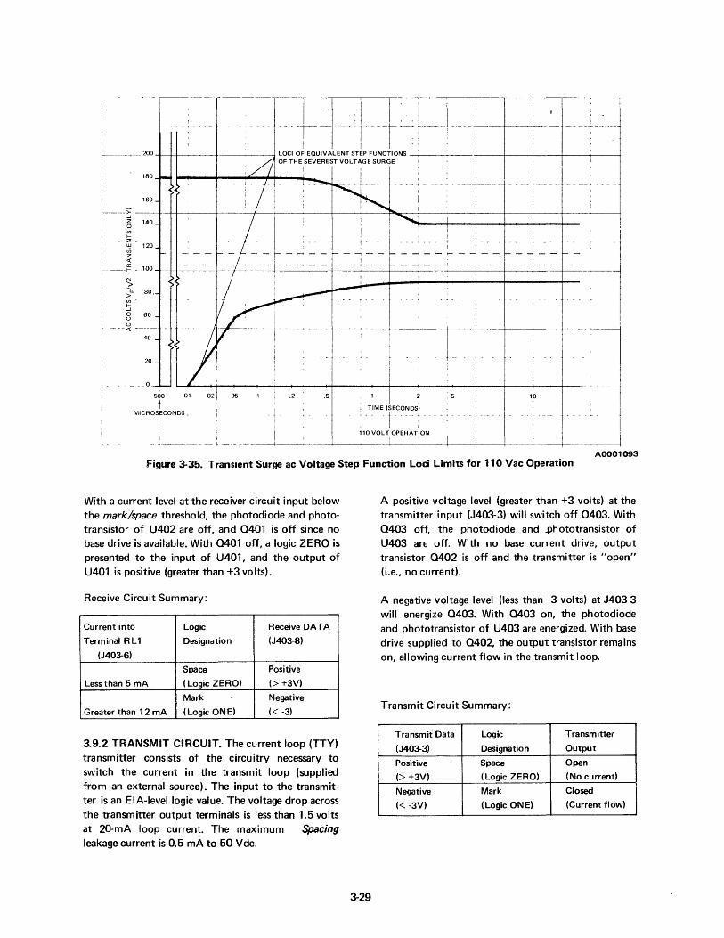
~ ------~--
I I _ 1 ____ _
. j .\ I ---~- '--~ ------ -r~------ -~- 1--- - -- - - f------- -~-_____r__---
I Ii! r- 200 +--++~~-+---+-~~ LOCI OF EQUIVALENT STEP FUNCTIONS --+--+---+-------i---tl--+-----+-----+
[
' -__ ~~ . /Ii OF THErSEVEREST VOLT~GE SURGE I . 180 '/ / , I -, . II r~r'K-
___ >: 160_ >"i
I ~ 140 - ~--"I __ +-__ ""i' ------11------+-
I Z - t - - - - J. I ~ 120 - ~ - - - - - - ~ - - I- - ~ - - - - ~ - - ,.... - -. - - I- - - - - - -
r--~-~-~ - 100 _ -:-__ _-_=-----=-_=-=- - -__ -_+-__ -_-_-_-__+~---~----_+_------t~.---_-_+ ...... _-__ 4"---_-----i~_-_~_r_---__+----~~----
I ~ S< , >0.. 80
enf.J a u u
60
-- -- <t: ~----
r-l----"- I
)( -~ 40 _
20 _
- -- 0 -.~ L........~___4_+__---+-+__---.j_---__ _+--_+_-_+--...... -_+_-___4--+_---____l
5tO 01 021 05 .2.5 I TIME (SECONDS') I 10 I "'C RO'!"ON 05 - - j - . -1- ... ; . - - , ... -I' I
_____ 0 ____ J _____ --+---,_,-O V __ O_L_TII-°_PE_R_AT_I_ON _ __+----_+_I _~_i~~ ~ A0001093
Figure 3-35. Transient Surge ac Voltage Step Function Loci limits for 110 Vac Operation
With a current level at the receiver circuit input below the mark/space threshold, the photodiode and phototransistor of U402 are off, and 0401 is off since no base drive is available. With 0401 off, a logic ZERO is presented to the input of U401, and th~ output of U401 is positive (greater than +3 volts).
Receive Circuit Summary:
Current into Logic Receive DATA
Terminal R L1 DeSignation (J403-8)
(J403-6)
Space Positive
Less than 5 rnA ( Logic ZERO) (>+3V)
Mark Negative
Greater than 1 2 rnA (Logic ONE) « -3)
3.9.2 TRANSMIT CIRCUIT. The current loop (TTY) transmitter consists of the circuitry necessary to switch the current in the transmit loop (supplied from an external source). The input to the transmitter is an EIA-Ievellogic value. The voltage drop across the transmitter output terminals is less than 1.5 volts at 20-mA loop current. The maximum Spacing leakage current is 0.5 rnA to 50 Vdc.
3-29
A positive voltage level (greater than +3 volts) at the transmitter input (J403-3) will switch off 0403. With Q403 off, the photodiode and .phototransistor of U403 are off. With no base current drive, output transistor Q402 is off and the transmitter is "open" (i.e., no current).
A negative voltage level (less than -3 volts) at J403-3 will energize 0403. With 0403 on, the photodiode and phototransistor of U403 are energized. With base drive supplied to 0402, the output transistor remains on, allowing current flow in the transmit loop.
Transmit Circuit Summary:
Transmit Data Logic Transmitter
(J403-3) Designation Output
Positive Space Open
(>+3V) (Logic ZERO) (No current)
Negative Mark Closed
«-3V) (Logic ONE) (Current flow)

3-10 FIRMWARE. The basic microprocessor control electronics consists of the central processing unit (CPU) integrated circuits, its ROM and RAM, the input/output (I/O) device, control logic for communication between the CPU and I/O, and buffers for communication of data between the I/O and the control devices. A block diagram of the firmware control system is shown in Figure 3-36. The I/O and timer devices are shown in Figure 3-37.
The ROM is used for program and table-lookup storage. The 64 words of RAM are utilized for program stacking and for software flags, counters, etc. Address decoding logic is included to supply enable signals for the ROM, RAM, I/O, the I/O output buffers, and the printhead line buffers.
The central processing unit (CPU) controls the operations of the I/O through firmware commands. These commands are decoded by the I/O chip from the CPU control signals and five address bus lines from the CPU. The firmware commands include read receiver buffer, read input bus, read interrupt reset ROM, read I/O status, load discrete commands, load baud rate command, load tl'ansmit buffer, load output register, load interrupt mask register, and load one of five timers.
After loading the I/O output bus and outputting the
correct address, the CPU scans the keyboard one row at a time. After outputting the scan the CPU then reads the I/O input bus to determine the status of the eight keys scanned in that particular row. In the same manner, but with a different address, the CPU controls the printhead stepping motor, the printhead pressure and line feed devices, and the bell.
The printhead line buffers are controlled solely by the CPU address lines. The appropriate data is output on address bits 12 to 15 to the address decode logic to generate a printhead strobe, and the particular printhead line buffer data is output on address bits 0 to 11, thus heating the appropriate printhead elements to create visible images on heat-sensitive printing paper.
The normal state of the CPU is the halt state. The CPU is interrupt-driven out of the halt state when processing is required. An interrupt forces the. CPU to one of eight different trap locations. Power-up may be considered an interrupt since it occupies trap location O. These interrupts are generated within the I/O device but can be controlled by the CPU. The CPU can disable or enable all interrupts, or it can enable any combination of them by loading the interrupt mask register.
The firmware package is an operating system responsible for Model 743/745 Data Terminal operations.
8080
CENTRAL PROCESSOR
UNIT
ADDRESS LINES (12)
Y7
Y6
Y5
Y4
Y3
Y2
Yl
a-BIT INPUT BUS
MULTI· PLEXER
(CPU)
__ J3~ __ _ ADDRESS DECODE
RAM
MOTOR TACH
a-BIT OUTPUT BUS
'-----__ XMIT DATA
MATRIX KEYS
KEYBOARD
FUNCTION KEYS
DRIVER
BUFFER
7 LINES
Xl X2 X3 X4 X5
FAST TO PRINTHEAD STEP STEPPING
PHASE A MOTOR DRIVE CIRCUIT
PHASE B
PRINT }
'-______ PHASE C
BELL
} LINE FEED AND HEAD PRESSURE
AOO01095
Figure 3-36. Model 743/745 Firmware Control System Block Diagram
3-30

+5V GND +12V -5V 01 02
------------------------------ -- -- -- -- ---------------- ------ -----!--------i------ --!- --- ----!--------t-------t---- --------INTERRUPT __ ~ ____ --.
CHIPSEL
SYNC
ADDRESS
CONTROL
LOGIC
(0-3) (4) _ .. --------
DATA .... (.8) •• BUS ..
B U
R
INTERVAL TIMERS
(5)
INTERRUPT STORAGE REGISTER
l..-___ RCV. INT.
l..-_____ XMT INT
(t) ...... (8.) •• ~~:~:SNAL ----~. BIT 7
(8)
EXTERNAL OUTPUTS
l..-_________ ~- XMT. DATA
RCV DATA
SENSOR
...... ____ .. __ .. ____ ... ___ .......... ____ ..... ___ ..... __ ..... _____________________ .... __ ................... ______ .. _ ...... _____________ ... _ .. ________ ... ______ ... __ .... _____ ... ________ I
A0001096
Figure 3-37. Functional Block Diagram I/O and Timer Device
For purposes of discussion, the operating system may be divided into several major subsections as shown in Figure 3-38. The power-up routine initializes all system pointers and flags and starts the keyboard scanner routine. The keyboard scanner routine detects key depressions and encodes them into ASCII characters, and the data control routine directs the characters to the appropriate processing program. The transmitter routine generates parity and transmits characters. The character analyzer routine determines if the mechanism is busy and, if not, passes the character to the appropriate processing subprogram_ If the mechanism is busy, the character is queued for later processing.
The operating system is provided with eight interrupts; five interrupts are used by the software system. A brief description of each interrupt is listed in Table
3-31
3-4. The software system is divided into three operating levels. The base level (when no interrupts are occurring) . is a halt state. All Model 743/745 processing is done in response to an interrupt. No activity occurs at the base level. The next level is composed of the keyboard timer interrupt and the receiver interrupt.
The receiver and keyboard routines can only interrupt the processor when it is in the halt state; neither routine can interrupt the other. The highest level is composed of the two timers associated with printing/ stepping and the sensor interrupt. These routines can interrupt the processor out of the halt state, keyboard scanner, or receiver routines. Routines running at the highest level cannot be interrupted. This three-level interrupt system is implemented by controlling the contents of the interrupt mask register in the I/O device.

Trap I 0
2
3
4
5
6
7
POWER-UP
BACKSPACE r--SUBROUTINE
CARRIAGE RETURN
SUBROUTINE
CHARACTER ANALYZER ROUTINE
j l
PRINT/STEP SUBROUTINE
KEYBOARD SCANNER
I
DATA CONTROL
LINE FEED r- SUBROUTINE
I
BELL SUBROUTINE
I
Figure 3-38. Model 743/745 Firmware Structure
Table 3-4. Firmware Operating System Interrupts
RECEIVER
I
TRANSMITTER
AOO01097
Location (HeX) I Name I Function
00 Power-up Activates the power-up initialize routine
08 Timer 2 Used for step timing
10 Sensor Feedback for motor control
18 Timer 3 Used for print/step timing
20 Receiver Character received by I/O
28 Transmitter Transmit buffer empty (not used)
30 Timer 4 Keyboard scanner timer
38 Timer 5 Spare timer
3-32

3.10.1 POWER-UP ROUTINE. When the POWER switch is first set to ON, the power supply generates a reset to the CPU. This starts the CPU with interrupts disabled at trap location 0 or at address 0000. The purpose of this routine is to:
(1) Initial ize the necessary RAM locations such as flags, counters, pointers, etc.
(2) Reset the I/O
(3) Set up the CPU stack pointer
(4) Start the keyboard scanner
(5) Begin machine functions such as line feed and returning the printhead to column 1 by performing backspaces.
The CPU then enters the halt state and waits for more work in the form of interrupts.
3.10.2 KEYBOARD ROUTINE. The keyboard routine scans, encodes, and debounces keys. After each key entry keyboard reports to data control the status of the function keys and whether or not a valid key has been detected in the keyboard matrix. The keyboard matrix is diagrammed in Figure 3-39.
3.10.2.1 Scanning (Standard ASCII). I n the keyboard routine three unique time periods are defined:
(1) Search period = 4 msec
(2) Debounce period = 11 msec
(3) Wait period = 11 msec.
The time at which the keyboard routine is re-entered is determined by one of these three modes. For the search and debounce modes, a scan takes place upon every entry. The wait period is utilized when a PAPER ADVance is pressed or when a character is
COLUMN
Co C, C2 C3 C4 C5 C6 C7
FS < GS = RS > us HERE Ro REPEAT
IS / 0
# $ % & R1 2 3 4 5 6 7 8 9
+ SOH
R2 A
3: STX ETX EOT ENQ ACK BEL BS HT
0 R3 B c 0 E F G H a::
LF VT [ FF \ CR ] SO " SI OLE @ DCf
R4 J K L M N 0 P Q
DC2 DC3 DC4 NAK SYN ETB CAN EM
R5 R s T U V W X Y
SUB PAPER
R6 Z LF CR DEL ESC SPACE BREAK ADVANCE
LEGEND NOTES
CONTROL SHIFT 1. NUMERIC MODE KEY CODING IS NOT SHOWN.
2. SHADED BLOCKS DENOTE KEYS PRESENT ONL Y ON FULL-ASCII KEYBOARDS.
UNSHIFTED CHARACTER
AOOO1098
Figure ~39. Model 743/745 Keyboard Matrix Encoding Scheme
3-33

repeating. Upon an initial detection of paper advance, scanning is inhibited for 20 wait periods. While repeating a character, scanning takes place only once every third wait period. When a second key (other than the R EPT key) is detected in the matrix, the scanning process is immediately stopped and the keyboard routine reports to data control that no new key was detected. Otherwise, when one or no key is pressed, a complete scan of the matrix occurs. The scanner utilizes a row and column counter so that when a depressed key is detected, row and column location data is recorded for use in encoding. Function keys are read and their status reported to data control upon every entry into the keyboard routine.
3.10.2.2 Scanning (APL/ASCII). The APL keyboard employs the same three time periods (listed above) used by the standard ASCII keyboard, but the APL keyboard has no REPEAT key. The APL keyboard repeat function is, instead, implemented by holding a valid key depressed longer than 0.5 second. The keyboard routine scans the matrix and, if a key is held depressed longer than one scan time, a wait period is initialized for 0.5 second. After 0.5 second if the key is still depressed, the next scan !ime will be set for 4 msec and the character represented by the depressed key will be repeatedly printed at a 10-CPS rate until the depressed key is released. All other APL keyboard scanning functions are identical.
3.10.2.3 Debounce. A debounce period, defined as 11 msec, occurs upon make and break of a key. Debounce of make-of-a-new key and break-of-anold-key may occur simultaneously. When the CPU is not in the debounce mode, it is considered in the search mode which lasts 4 msec. The search mode occurs also for both make and break, and like debounce, search-for-make-and-break may also occur simultaneously. Therefore, if two keys are pressed almost simultaneously, the second key need only be pressed 4 msec past the break bounce of the first key. The PAPER ADVance and R EPT keys are not debounced.
3.10.2.4 Encoding (Standard ASCII). When a new key depression is detected in the matrix, it is encoded immediately. [REPT (repeat), HERE IS, BREAK, and PAPER ADVance are not ASCII-encoded keys.} In the NUMbers mode the row/column data is used to obtain the ASql code from a look-up table; five special keys are similarly encoded: LINE FEED, carriage RETURN, RUB OUT, the space bar, and ESC. All other keys are positioned in the matrix so that the addition of a constant number to the
3-34
row/column number of each key will provide the ASCII code for that key in the unshifted mode. For the CTRL (control) and SHIFT modes the ASCII code is obtained by adding or subtracting an appropriate number depending upon the particular key. After encoding, the new ASCII character is passed to data control for immediate action. Encoding occurs upon detection and not after debounce of the key.
3.10.2.5 Encoding (APL/ASCII). When the APL keyboard is in the APL mode, shifted and unshifted, the row/column data is used to obtain the ASCII code from a look-up table. Encoding in the full-ASCII mode, shifted and unshifted, and in the CTR L (control) mode is identical to standard-ASCII keyboard encoding described above.
3. 10.2.6 Repeat Function. Any printable character may be repeated by pressing a character key in conjunction with the REPT key (except for the APL keyboard). The character will be printed continually until the R EPT key is released. Pressing a new key causes its character to be repeated as long as the REPT key is held depressed.
3. 10.3 RECEIVER ROUTINE. Upon recelvmg a full-ASCII character the I/O device transfers the character from the receiver register to the receiver buffer and generates an interrupt to the CPU. The CPU then removes that character within 30 msec to prevent loss. The sale purpose of the receiver routine is to fetch the character from the receiver buffer and pass it to data contro I.
3.10.4 DATA CONTROL ROUTINE. Data is supplied to the Models 743/745 from two sources: the keyboard and the receiver. Hence, the data control routine has two major divisions: keyboard data control and receiver data control.
3.10.4.1 Keyboard Data Control. The first function of keyboard data control is to update the baud rate status to the I/O and to update the local flag status in RAM. It then decides whether or not the keyboard has any new data; if not, data control is exited. Transmission of a new character occurs if the terminal is on-line and the transmitter is not busy. The character is transferred to the character analyzer to determine what printer action is to be taken if the terminal is in the local mode or if the transmitter is not busy and the terminal is in the half duplex mode.
3.10.4.2 Receiver Data Control. A received character is sent to the character analyzer if the terminal is in

the on-line mode, if at least two spaces remain in the eight-character printer character queue buffer, and if the paper-out count is not 5. Otherwise, the character is ignored and no action is taken.
3.10.4.3 Print Complete. After completing a printer action, all printer software routines enter print complete. This terminates the printer action and indicates that the mechanism is free. Print-complete
detects any character that might have been stored in the printer queue buffer and passes it to the character analyzer for processing.
3.10.5 CHARACTER ANALYZER. The character analyzer accepts a character from either data control or print-complete and determines what printer action should be taken. A BEL character immediately starts the audible signal. No action is taken on a DELete or NUL character. If the mechanism is not busy, the following procedure is taken on all other characters. Printable characters enter print state 1 and immediately start printing. CR, LF, and BS enter appropriate printer states, but all other control characters are ignored. If the mechanism is busy, the character is stored in the printer character queue buffer (eight-
character capacity) for later processing.
3.10.5.1 Bell Routine. The time interval for the audible signal to sound upon receipt of a BEL character is 250 msec. To time this period the bell routine utilizes the keyboard timer. When a BEL character is received, a counter is set to the appropriate value and the audible signal is energized. The keyboard routine then decrements this counter at each entry and when the count reaches zero, the audible signal is switched off.
3.10.5.2 Print/Step Routine. The print/step routine generates the pulse train shown in Figure 3-40. The routine can be divided into two sections. The first section energizes the printhead voltage (PVOL T), indexes into the dot matrix table (stored in ROM) by the ASCII character value, chooses the appropriate dot pattern, and loads the printhead one column at a time. Loading is accomplished by generating an address which includes the printhead strobe bit, the column being loaded, and the column dot pattern. The printhead is loaded during the first 200 psec of PVOL T-on. The PVOL T signal remains on for 10 msec.
PRINT f-~t-+-+-- -4 J - - - -, : + t ~- 1-1 -i-- L- -t-4 +i h--t+ ~+~-+ -t- -r '-1 +- ~~ ~ ~_ - - -"-_.~ 'I -T--;-~-+--t r: - • - . - t ----~-~ -tt-i- ~-+ 1 j r t-t +1- Tt +H:- ~ -r--r ~ r, 1---- -~ +"- - c---l- _1-_
_ +----+-_l-_____+_ ~-+ -+ i" -----+ --.- -.... +- -+ t _L I -+-- +- + -+-- -----t -t,-,
;t-+-~ -- -.. - ' - -+-. -+tl-i- , t .-+ -+-~ ~+ +- ~ -:- --+- L+ ~-+-~---~-+ ~~-+-~ ->-T·-~---.-:._L + + -+--+- - 1" + -1--:-- +-__ L __ +~_
FAST
STEP -+ + -.. -~
+- ~ -. +-
SENSOR .. 4- +- t
--<.--+ +
I ! ' ~ t +i r-H-:
+- t--- t +-1 -f T -+f +--t- -+- +--+-1-- t,
.L t -t t ... t--i -l- +-+---+ t - .-It + ~ -.-I-+-
- ~- -~-i---!
PHASE B c--:-t ~T-ht ' : t-t t-1 -T4-+~ - t- i -+ -r-; t:~JT-~
_J : _ 4_ 1 1 L _
+ 1 ~ 4-- i -..... i--,
; -. - 1 -- -T-t--I---..l_-+ - -~ + +--'--+-i-~
'-r-t -1--+, -+-- -~ t :--;-J--__ __ -t-_':'-~ _____ _ _Ll-, __ ~ I ',__" _! _ _ 1 __ 1__ 1 _ _ ~ __ ! :
Figure 3-40. Models 743/745 Print/Step Routine Pulse Train AOO01099
3-35

The second section steps the printhead one column by using two timers and the sensor. One timer is used to control pulse widths for the fast and step pulses. The sensor signals the beginning of braking. The second timer is used to time the total step and is divided into two segments: the first verifies that the sensor occurred, and the second segment defines the end of the step. The use of the second timer makes the step time independent of when the sensor interrupt occurs. Figure 3-41 shows a state diagram of this sequence.
3.10.5.3 Backspace Routine. The backspace routine uses the step section of the print/step routine. The only difference is that the phase is calculated to cause the printhead to step left instead of right.
3.10.5.4 Line Feed Routine (Solenoid Line Feed Mecrranism). The line feed routine energizes the printhead lift and .Iine feed solenoids for 15 msec, then off for 16.8 msec. This causes the paper to advance one line.
3. 10.5.5 Line Feed Routine (Stepping Motor line Feed Mechanism). The line feed routine energizes the line feed stepping motor by alternately energizing the LF-step A and LF-step B drivers. Each driver phase is energized twice for 6 msec each, producing a complete paper line feed comprising four step segments of 7.5 degress each for a. total 30 degrees. Figure 3-42 shows a stepping motor timing diagram.
3. 10.5.6 Carriage Return Routine. A carriage return from column one causes no action. A carriage return from column two is treated as a backspace. Printhead lift is activated until the printhead reaches column two. Stepping current remains on throughout the carriage return to provide the motor sufficient current for acceleration and deceleration. Speed control during carriage return is accomplished by changing phases on the motor feedback sensor (acceleration) or by changing phase after the feedback sensor (deceleration). Figure 3-43 is a state diagram of the carriage return algorithm.
a. Acceleration Outside Column 20. In the carriage return routine the timer value is set to 1.5 msec. Since the motor is stopped, the timer will expire and cause an interrupt before the sensor reacts. Motor phases are changed when the sensor reacts, causing acceleration of the motor. Five 1-msec pulses are generated
3-36
b.
c.
d.
during the first five steps of acceleration to provide quick acceleration.
Constant Speed Control. Once the feedback sensor signal occurs faster than 1.5 msec, the motor phase change occurs when the timer expires, decelerating the motor. Acceleration and deceleration are used for the constant speed region. Note that the change from acceleration (paragraph a. above) to constant speed occurs without a firmware change of state.
Deceleration at Column 12. When the printhead reaches column 12 and the phase change to move to column 11 is output, the firmware detects that it is time to decelerate. Instead of setting the timer to 1.5 msec, a longer time is used. For each column throughout the de~eleration period, a successively longer time is used when setting the timer. This causes the motor phases to change on the timer, initiating deceleration. The values in the deceleration table were selected to decelerate the motor along a profile which resembles the natural deceleration of the system.
Acceleration/Deceleration Inside Column 21. A different rate of acceleration is used for each column- inside column 21. A slower acceleration enables the processor to intercept the deceleration profile and bring the printhead to a smooth stop. This time is used until a column is reached inside column 12 where its deceleration time is longer. This represents the point where the deceleration profile is intercepted and deceleration begins.
3.10.6 CHARACTER BUFFERING. There are several advantages to the use of character buffering in a data termi nal. Using a character buffer to store a received character while the mechanism is busy eliminates need for the traditional filler characters sent after a carriage return. To implement such a scheme the print/step time of the data terminal must be less than the time consumed to receive a character. Character buffering increases input to the terminal byeliminating the transmission time used to send filler characters. Interfaces to the data terminal are simplified

FAST OFF
. SENSOR DELAY
FAST ON STEP OFF LAST PHASE ON
FAST OFF STEP ON LAST PHASE ON
STEP OFF LEAVE NEXT PHASE ON
PVOLTON LOAD PRI NTHEAD
PVOLTOFF FAST/STEP ON NEXT PHASE ON
END OF PRINT/STEP CYCLE
Figure 3-41. Print/Step Routine State Diagram
3-37
SENSOR FAILURE
AOOO1263

LFSTEPA J LF STEP B
(CRST4)
(CRSTF)
~@ 6 msec I 17
5 SETTLING
"4 :. msec TIME
(ONE LlNE-FEED)------II~ .... 4I1--NEXT CHARACTER --....
Figure 3-42. Stepping Motor Line Feed (IF) Routine Timing Diagram (Mechanism PIN 999257)
(CRST2)
ACCELERATION DECELERATION
DECELERATION
(CRTYT2)
Figure 3-43. Carriage Return Routine State Diagram
3-38
(CRST4S)
DECELERATION
(CRS4S2)
A0001101

since the transmitting system does not need to recognize certain control characters which require special handling. Because of the desirability of character buffering and the ability of the Models 743/745 to perform a print/step cycle in 28.5 msec, an eight-character buffer is designed into the operating system.
3.10.7 PAPER ADVANCE OPERATION. The paper advance (PA) function is generated by the keyboard routine. Upon an initial detection of the PAPER ADV key, the terminal is forced OFF LINE, a carriage return character (CR) is generated, and scanning is inhibited for 20 wait periods. The PA flag is set, and the carriage return character is processed. As long as the PAPER ADV key is depressed, the keyboard scanner sets the PA flag and generates a CR character every third wait period. At the end of the CR, the PA flag is checked and control transfers to the line feed routine.
The line feed routine causes one line feed and clears the PA flag. A continuous stream of line feeds then are executed as long as the PAPER ADV key is depressed. Received characters will be lost since the terminal is forced into an off-line mode.
3.10.8 ANSWER-BACK MEMORY. The Answer-Back
Memory (ABM) option for the Models 743/745 Data Terminals transmits any programmed sequence of one
to 21 ASCII characters to serve as station identification. The character string, along with the system software to implement the ABM feature, is included in a 256 x 8 PROM (74S741) which plugs into a socket on the PWB. The message sequence is activated by the HERE IS key or by receipt of an ENO character if the terminal is on-line. An optional bit in the PROM indicates to the ABM system program if the ABM message is to be printed when operating in the half-duplex mode.
Following is a list of operating characteristics of the ABM option:
• Activated locally by HERE IS key if the terminal is ON LINE
•
•
Activated remotely by receipt of the ENO character if ON LINE
While in an ABM sequence, operation of the HERE IS key or receipt of an ENQ character will not cause the ABM sequence to restart
3-39
•
•
•
•
•
•
If the terminal is taken OFF-LINE during an ABM sequence, the sequence will be aborted
The ABM sequence cannot be activated if the terminal is performing a paper advance.
If the terminal is in the half-duplex mode and the option to print the ABM message is set, the ABM message will be transmitted and printed. Characters received during the printing of the ABM message will also be printed.
During an ABM sequence, characters generated at the keyboard are ignored.
Parity is generated based on the strappable option on the PWB (factorysupplied only).
If the BREAK key is already activated when an ENO character is received, the ABM sequence will start; but the transmitter will not transmit the characters because it is in the BREAK mode. If the terminal is in the half-duplex mode and the option to print is enabled, the message will be printed.
3.10.9 LEFT MARGIN/PAPER-OUT DETECTION. During the step sequence, the print/step routine can detect a sensor failure. During normal operation, sensor failures indicate an attempt to step the printhead through an abnormally high friction area (left margin stop or stepping the printhead with no paper between it and the drive roller). This information is used to detect both left margin and paper-out in the Model 743/745 operating system.
3.10.9.1 Left Margin Detect. During power-up, the printhead is stepped to the left by performance of repeated backspaces. A sensor failure is generated when the printhead is stepped against the left margin. Sensor failure also occurs if the motor is told to step to the phase it already is in. By forcing the printhead
to step at least three steps during power-up, the operating system gets in step with the motor and the next sensor failure after the initial three steps is considered the left margin.
3.10.9.2 Paper-Out Detection. During step operations after power-up, a sensor failure will activate the
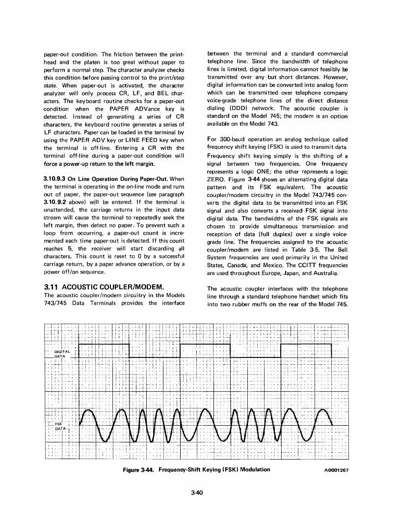
paper-out condition. The friction between the printhead and the platen is too great without paper to perform a normal step. The character analyzer checks this condition before passing control to the print/step state. When paper-out is activated, the character analyzer will only process CR, LF, and BEL characters. The keyboard routine checks for a paper-out condition when the PAPER ADVance key is detected. Instead of generating a series of CR characters, the keyboard routine generates a series of LF characters. Paper can be loaded in the terminal by using the PAPER ADV key or LINE FEED key when the terminal is off-line. Entering a CR with the terminal off-line during a paper-out condition will force a power-up return to the left margin.
3.10.9.3 On Line Operation During Paper-Out. When the terminal is operating in the on-line mode and runs out of paper, the paper-out sequence (see paragraph 3.10.9.2 above) will be entered. If the terminal is unattended, the carriage returns in the input data stream will cause the terminal to repeatedly seek the left margin, then detect no paper. To prevent such a loop from occurring, a paper-out count is incremented each time paper-out is detected. If this count reaches 5, the receiver will start discarding all characters. This count is reset to a by a successful carriage return, by a paper advance operation, or by a power off/on sequence.
3.11 ACOUSTIC COUPLER/MODEM. The acoustic coupler/modem circuitry in the Models 743/745 Data Terminals provides the interface
between the terminal and a standard commercial telephone line. Since the bandwidth of telephone lines is limited, digital information cannot feasibly be transmitted over any but short distances. However, digital information can be converted into analog form which can be transmitted over telephone company voice-grade telephone lines of the direct distance dialing (DDD) network. The acoustic coupler is standard on the Model 745; the modem is an option available on the Model 743.
For 300-baud operation an analog technique called frequency shift keying (FSK) is used to transmit data.
Frequency shift keying simply is the shifting of a signal between two frequencies. One frequency represents a logic ONE; the other represents a logic ZERO. Figure 3-44 shows an alternating digital data pattern and its FSK equivalent. The acoustic coupler/modem circuitry in the Model 743/745 converts the digital data to be transmitted into an FSK signal and also converts a received FSK signal into digital data. The bandwidths of the FSK signals are chosen to provide simultaneous transmission and reception of data (full duplex) over a single voicegrade line. The frequencies assigned to the acoustic coupler/modem are listed in Table 3-5. The Bell System frequencies are used primarily in the United States, Canada, and Mexico. The CCITT frequencies are used throughout Europe, Japan, and Australia.
The acoustic coupler interfaces with the telephone line through a standard telephone handset which fits into two rubber muffs on the rear of the Model 745 .
. : : : t : --:-: • • ~- +
Figure 3-44. Frequency-Shift Keying (FSK) Modulation AOO01267
3-40

Table 3-5. Acoustic Coupler/Modem FSK Transmission Frequency Assignments
Frequencies (Hz)
Logic Bell System CCITT Lavel XMIT I RCV XMIT 1 RCV
"1" (MARK) 1270 2225 980 1650
"0" (SPACE) 1070 2025 1180 1850
One muff contains a microphone; the other, a speaker. The interface is entirely acoustic.
The modem (available as an option only on the Model 743) interfaces directly with the telephone line via a transformer contained within a data coupler (DAA) required to connect the modem to the telephone line. A block diagram of the acoustic coupler/modem is shown in Figure 3-45. A schematic of the circuitry is contained in the appendix.
Note that the modem and acoustic coupler share most of the same circuitry; for this reason the
operation of the acoustic coupler is described first and the differences between the acoustic coupler and modem are discerned where appropriate in the text.
3.11.1 RECEIVER SECTION. The receiver section of the acoustic coupler/modem consists of a buffer, bandpass filter, limiter, mark and space filters, difference integrator, data filter, carrier detector, and carrier detect delay circuits. The microphone is connected through the buffer (a high gain amplifier) to a bandpass filter which passes in-band signals and attenuates out-of-band signals and noise, thus providing some selectivity. The output of the bandpass filter is applied to the limiter which provides a constant amplitude signal to the mark and space filters. The mark filter's greatest output occurs when the mark frequency is received, and the space filter's greatest output occurs when the space frequency is received.
The output of the mark and space filters is appl ied to a difference- integrator which determines which filter has the most output over a bit time. The difference integrator's output is applied to the data filter and carrier detect circuit. The data filter smoothes the
r---------------------------------------------------r----~OPHONE 1
I I I I I I It'
I MODEL 745 >-...... -...&00 ...
! ACOUSTIC COUPLER
DATA TRANSMITTER
AOO01270
HALF DUPLEX MODE
RECEIVED DATA
(ASSEMBLY 937300)
_ CARRIER DETECT
I I I I I
MODEL 743 MODEM OPTION
DT} MODEL 743 MODEM OPTION DR
------------, I SPEAKER I
I MODEL 745 1.. __ ACOUSTIC COUPLER
I I I I ...
Figure 3-45. Acoustic Coupler/Modem Block Diagram
3-41

difference integrator output and converts the signal to ±1 G-volt levels. The carrier detect circuit determines whether an in-band or out-of-band signal is present at the input of the receiver.
An in-band signal starts a 3-to-7-second delay in the carrier detect delay circuit before it provides a valid carrier indication to the terminal and enable transmitter circu it. An out-of-band signal starts a 100- to 3OG-millisecond delay before a no-carrier indication is provided to the terminal and transmitter.
On assembly 937300 only, jumper E425/E426 provides a long or short carrier detect delay. Installed, the delay is 3 to 7 seconds. If not installed, the delay is 1 to 2 seconds.
The signal input to the acoustic coupler is an audible tone emitted by the telephone handset. This FSK signal is converted to an electrical signal by the microphone. The incoming signal then is amplified by the buffer amplifier (U413, R501, R500, and R495)' the gain of which is determined by R501 and R495.
The signal then goes to a three-stage stagger-tuned bandpass filter which amplifies in-band signals and attenuates out-of-band signals and noise. The first stage of the filter (U413, R491, R494, R502, C428, and C427) has a nominal center frequency of 2345 Hz, a gain of 14 dB and a Q of 5. The second stage of the bandpass filter (U407, R489, R490, R450, C418, and C417) has a nominal center frequency of 1915 Hz, a gain of 14 dB, and a Q of 5. The last stage of the filter (U406, R446, R429, R445, C412, and C411) has a nominal center frequency of 2125 Hz, a gain of 3 dB and a Q of 5.
The composite filter response yields an overall gain of 25 dB with relatively linear phase characteristics and a 30G-Hz bandwidth. The linear phase characteristics contribute to equal mark and space frequency delays.
The limiter (U406, R442, R444, CR408, CR409) produces a constant amplitude (±0.7 volt, peak-topeak) input signal for the mark and space filters by limiting the positive and negative excursions of the output with CR408 and CR409.
The bandwidth of the incoming signal at 300 baud is 300 hertz, centered about the carrier frequency of 2125 Hz (1750 Hz for CCITT). To receive signals of
this bandwidth, the mark filter is nominally tuned to 2275 Hz, and the space filter is tuned to 1975 Hz. Both filters have equal gains, and the envelope delay at the center frequency of each filter is equal.
• 3-42
The difference integrator circuitry determines which filter has the most output over a bit time. The outputs of the mark and space filters are subtracted by CR413, R476, CR416, and R479 and by CR415, R481, CR414 and R474. When a mark is received, the output of U410 (pin 1) is in positive saturation; similarly, when a space is received U410 (pin 1) is in negative saturation. Under no-signal conditions, the output of U410 is nominally zero volt.
The data filter stage, R455, R554, and C413, form a low-pass filter which removes any carrier frequency signals still present on the output of the difference integrator. The remaining components of the data filter (U410, R454, and R453) constitute a comparator with hystersis. The output of U410 (pin 7) is in negative saturation for a mark and in positive saturation for a space.
On assembly 937300 only, the receive-data signal is held in the mark condition whenever the carrier detect delay output signal is off (-12 volts), indicating absence of a valid carrier signal.
3.11.1.1 Carrier Detect. The carrier detect circuit determines if a valid FSK signal is being received. The carrier detect circuit receives its input signal from the output of the difference integrator (U410, pin 1) which is +10 volts or -10 volts when a signal is received or zero volts when no signal is received.
Under a no-signal condition U404 (pin 1) is +10 volts since U404 (pin 2) is pulled to -12 volts through R423, and U404 (pin 3) is at zero volts. When the output of the difference integrator exceeds +2 volts, the input (U404, pin 2) becomes more positive than pin 3 (U404), and the output (U404, pin 1) switches to -10 volts.
Similarly, when the output of the difference integrator ranges between the negative saturation voltage of U410 (pin 1) and -5 volts, the noninverting input of the carrier detect op-amp (U404, pin 3) is more negative than the inverting input (U404, pin 2), so the output switches to -10 volts. To prevent a loss of carrier indication while receiving data during which the output of the difference integrator is switching between +10 and -10 volts, the voltage stored on C409 and C404 (in conjunction with the RC time const~nds of C409, R422, and R424 or C404, R402, and R403) are sufficient to prevent the output of U404 (pin 1) from switching to a no-carrier condition (+10 volts)_

3.11.1.2 Carrier Detect Delay. The carrier detect delay circuit generates the appropriate energizing and de-energizing delays required by the term ina!. A -10 volt signal from U404 (pin 1) indicates that a valid carrier is present. Since CR405 is reverse biased, capacitors C410 and C432* are charged to -10 volts through R426. An electronic jumper installed at E425-E426* provides normal turn-on and turn-off delays. With the E425-E426 jumper removed, shorter delays are provided_ (Only the standard 3 to 7 second -delay is available on PWB 983841.) R426, along with C410 and C432, determine the turn-on time of 3 to 7 seconds. With the short delay option (available only on PWB 937300) the turn-on time is 1 to 2 seconds. When the voltage across C410 is less than the -7.5 volt threshold of the comparator formed by U404, R404, R405, and R406; its output switches to +10 volts, indicating the presence of a val id carrier.
When the output of the carrier detect circuit (U404, pin 1) is +10 volts, C410and C432 discharge through R425 and CR405. R425, along with C410 and C432, determine the turn-off time of 100 to 300 milliseconds (50 to 100 mill iseconds with the short delay option). When the voltage across C410 is more positive than -4 volts, the comparator output switches to -10 volts, indicating absence of a val id carrier.
*NOTE Carrier detect delay jumper E425-E426 and capacitor C432 are supplied on PWB
937300 only.
3.11.1.3 Receive-Data Clamp (Not Available with the CCITT Option). The receive-data clamp circuit is provided to eliminate the effects of erroneous receive data caused by the transmitter second harmonic frequencies overlapping the bandwidth of the receiver. This circu it forces, or clamps, the receive-data signal to a mark condition whenever the transmit-data signal is in a space condition. The circuit is enabled only when the terminal is in the half-duplex mode.
With a -10 volt level at U405 (pin 1), the transmitter is in the space condition. Thus, CR428 is forwardbiased, and C431 charges toward -10 volts through R473. Buffer amplifier U415 (pin 1) tracks the capacitor voltage towards -10 volts, which causes the output of U1 (pin 8) to switch to +5 volts. This turns on 0551, which causes CR426 and CR427 to turn on, bringing U415 (pin 5) to approximately +1.5 volts. If the terminal is in the half-duplex mode, the output latch U25 (pin 7) is turned on and pulled to
3-43
+5 volts through R22. Thus, U415 (pin 7) is in negative saturation (-10 volts), causing CR425 to be forward-biased. This then forces, or clamps, the output of the difference integrator U410 (pin 1) to +10 volts, regardless of the receiver input signal. This causes the receive-data signal to be held in the mark condition, and holds the carrier detect signal on. When the transmit-data signal returns to the mark condition, U405 (pin 1) switches to +10 volts. This turns off CR428 and permits C431 to discharge toward +10 volts through R473 and R488. The output of U1 (pin 8) switches to ground, causing 0551 to turn off. This pulls U415 (pin 5) to +12 volts through R499 since CR426 and CR427 turn off. This causes U415 (pin 7) to switch to +10 volts, which turns off CR425, freeing the difference integrator and allowing it to switch with the incoming signal.
When the terminal is in the full-duplex mode, the output latch U25 (pin 7) is off and held near ground. Thus, since the noninverting input of U415 (pin 5) never falls below ground, the output of U415 (pin 7) always is +10 volts, which turns off CR425, effectively disabling the circu it during full-duplex.
3. 11.2 TRANSMITTER SECTION. The transmitter section consists of an FSK transmitter, including transm it-inhibit circuitry, a low-pass filter, a transmit-level adjustment, and hybrid.bridge circuits.
The FSK transmitter is a triangular-wave oscillator which oscillates at one of the two FSK frequencies selected by the digital transmit-data signal. The transmitter is enabled to oscillate only after a valid carrier is present and the carrier detect signal is on. The low-pass filter removes the higher order harmonics present in the triangular wave. The low-pass filter output is connected through the output level adjustment to the hybrid bridge.
When the PWB is configured as an acoustic coupler (Model 745), the hybrid bridge is used as a buffer amplifier to drive the speaker. When the PWB is configured as a modem (Model 743 option), the hybrid bridge permits the FSK transmit data to be
applied to the telephone line via the DT and 0 R leads. I n the modem configuration the received FSK data also is present on the DT and 0 R leads since it is a two-wire full-duplex system. The hybrid bridge not only applies the received FSK signal to the receiver input (as indicated by the dashed line on Figure 3-45), but it also isolates the transmitter section from the receiver section.

For purposes of discussion, assume that the output of U412 (pin 7) of the FSK transmitter is at -12 volts. CR412 is reverse biased, and CR411 is forward biased. A -4.3 volt reference (-6.3 volts on PWB 983841) is established by CR420, CR417, and CR419. The constant negative voltage at the input of the integrator (U407, C416, and the series combination of R472 and R448) causes the output (U407, pin 7) to ramp linearly positive with time.
When the output passes +4.3 volts (+6.3 volts on PWB 983841), the noninverting input of U412 is slightly positive because of the voltage divider formed by R487 and R485 between the negative reference and U407 (pin 7).
The positive voltage at U412 (pin 2) causes the output to switch to +12 volts, and a +4.3 volt reference (+6.3 volts on PWB 983841) is established by CR421, CR417, and CR418 at the input to the integrator. The integrator now ramps linearly negative until the output is slightly less than -4.3 volts (-6.3 volts on PWB 983841). The noninverting input of U412 is now slightly negative, so the output switches to -12 volts, and the cycle starts again.
In order to change the frequency of the oscillator, a shunt resistor (R447) is switched across the series combination of R472 and R448 by 0405. 0405 is switched on and off by the output level present at U405 (on during the mark frequency, off during the space frequency).
3-44
The transmitter is enabled and disabled using the carrier detect signal present at U404 (pin 7). When a valid carrier is present, U404 (pin 7) is +10 volts which turns on 0406 and turns off 0407. This enables the comparator U412, thus enabling the transmitter. While carrier detect is off, U404 (pin 7) is -10 volts, forcing 0406 off and 0407 on, which disables U412 and the transmitter.
3.11.2.1 Transmit Low-Pass Filter. The triangularwave output of the transmitter section is altered using a low-pass filter to lower the distortion by attenuating all harmonics of the fundamental frequency. The resultant output is a sine wave of approximately ±9 volts peak-to-peak.
3.11.2.2 Transmit Level. The output of the low-pass filter is applied through a 10k ohm potentiometer which determines the output transmit level. U414
(pins 1, 2, and 3) forms a buffer to drive either the speaker (acoustic coupler) or the duplexer (modem).
The duplexer (U414, pins 5, 6, and 7; R496, R498, and R499) provides the appropriate driving and term inating impedances to match the modem to the data access arrangement (DAA). The duplexer also provides isolation between the transmitter and receiver of the modem to prevent a strong transmitted signal from swamping a sl)1all received signal. Backto-back zener diodes (CR422, CR423) act as clippers to protect the DT and DR leads from high voltage spikes.

SECTION 4
MAINTENANCE
4.1 PREVENTIVE MAINTENANCE. The TI Models 743/745 Data Terminals are designed and built to provide long term trou ble-free operation under rigorous operating conditions. To ensure continuation of the highest performance levels, the machine should be cleaned at regular intervals. The printer mechanism and printhead should be kept
clean and free of foreign objects.
To ensure that the printer mechanism continues to provide maximum print quality, the printhead should be cleaned periodically as follows (refer to Figure 4-1 for location of components):
1.
2.
3.
4.
Remove the thermal paper from the platen and paper chute. If necessary, cut the paper where it enters the chute. Press and hold the PAPER ADV key until the short piece exits the window/pinch roller.
On a sheet of good quality bond paper, wet a 2- inch wide area with denatured alcohol (available from TI in pint containers, Part No. 230007).
Insert the alcohol-wetted paper through the paper chute, around the platen, and under the window/pinch roller. Use the PAPER ADV key to advance the bond paper.
Type four to six lines on the alcoholwetted area. Use the R EPT key to accelerate the process. Then advance the paper to a dry area and type two more lines.
NOTE The thermal printhead will not print visibly on conventional paper.
5. Press and hold the PAPER ADV key to remove the cleaning paper and reload the thermal paper supply.
4-1
The printhead should be cleaned as instructed above each time a new roll of paper is loaded into the printer. Clean the printhead more often if the printed images start to fade as a result of residue accumulating on the printhead.
4.2 TROUBLESHOOTING. Troubleshooting data terminal malfunctions is fac il itated by use of the flow diagrams starti ng on page 4-12 to help localize failures to a particular assembly. When one or more subassemblies are removed during the trou bleshooting process, each suspected subassembly should be reinstalled, one at a time, to verify it is indeed the cause of the failure. But in the case of a catastrophic failure, such as blown fuses, overheated or burned components, or other obvious physical defects, return the subassembly to the factory for repair and skip the verification step described above.
NOTE The troubleshooting diagrams are intended for use by trained service personnel.
4.3 ADJUSTMENTS. The Models 743/745 Data Terminals have only two field adjustments in normal use: print CONTRAST control and the coupler TRANSMIT LEVEL control. All other adjustments are completed at the factory and should not be changed.
4.3.1 PRINT CONTRAST. To adjust print image contrast, locate the CONTRAST potentiometer clearance hole on the right side of the terminal. Insert a small screwdriver through the clearance hole and gently rotate to seat the screwdriver in the screw slot.
a.
b.
To darken the printed image, slowly rotate the adjustment screw clockwise while printing characters from the keyboard until the desired contrast is achieved.
To lighten the printed image, rotate the adjustment screw counterclockwise.

MECHANISM SUPPORT POST
PLATEN
PRINTHEAD
PRINTHEAD MOUNTING SCREWS
MECHANISM SUPPORT POST
a. Unit With Solenoid-Driven Line Feed Mechanism
b. Unit With Motor-Driven Line Feed Mechanism (All other components are similar to Figure 4-1a.)
Figure 4-1. Models 743/745 Component Locations
4-2
PRINTHEAD
ADJUST WHEEL
LINE FEED SOLENOID
P1000027
LINE FEED MOTOR
PRINTHEAD SOLENOID ADJUST WHEEL (UNDER PLATEN DRIVE PULLEY)

4.3.2 ACOUSTIC COUPLER OR MODEM TRANSMIT ADJUSTMENT. This adjustment controls the transmit level of the signal applied to the tel~phone line. The transmit level is adjusted at the factory to produce -15 dBm (0 dBm = 1 mill iwatt dissipated in a 600-0hm load) on the telephone line after passing through the telephone handset from the acoustic coupler or -9 dBm after passing through the COT DAA from the modem.
The transmit level is factory-cali brated for optimum performance wi th most U.S. telephone systems. However, since handset quality differs and line losses occur in some telephone systems, it may be necessary
to compensate for unusual conditions by adjusting the transmit level.
The transmit level may be adjusted to accommodate different handsets and telephone systems as follows:
a. Locate the TRANSMIT LEVEL potentiometer clearance hole on the left side of the termi nal. I nsert a small screwdriver through the clearance hole and gently rotate to seat the screwdriver in the screw slot.
b.
c.
Establish contact with a remote terminal.
Slowly rotate the TRANSMIT LEVEL adjustment screw clockwise until the terminal begins to receive garbled data from the remote source. Reduce the level sl ightly to achieve error-free reception.
4.3.3 PRINTER SUBSYSTEM ADJUSTMENTS. Under normal operating conditions, the closed-loop control circuitry of the printer subsystems will compensate for friction changes caused by wear, temperature variations, and component aging., No field adjustments are required except alignment of . the thermal printhead after replacement of the mechanism or printhead assembly. If print quality deteriorates, do not attemp~' adjustments until the cause is fully understood.
Two versions of the printer subsystem are used on Model 743/745: one version (983811) employs a solenoid-actuated line feed; the other version (999257) is equipped with a motor-driven line feed. Both versions use a solenoid-actuated printhead pressure mechanism, but the solenoids are mounted and linked to the printhead pressure bar differently. The two versions may be differentiated as follows.
4-3
Data Terminal Serial No.
Mechanism Used
OX743YYYYYand OX745YYYYY
Solenoid-actuated line feed - Part No. 983811
OX744YYYYYand OX746YYYYY
Motor-driven line feed - Part No. 999257
4.3.3.1 Printhead Pressure Adjustment (Mechanism Part No. 983811).
a.
b.
c.
d.
e.
f.
Remove the inner cover from the terminal as instructed in paragraph 4.4.3 below.
Manually position the printhead approximately 4 inches from the left margin.
Manually compress the printhead solenoid (Figure 4-2a) so that the solenoid is in the fully energized position.
Place a measuring scale along the solenoid I inkage and measure the travel distance.
Adjust solenoid travel to at least 0.04 inch but no greater than 0.05 inch by rotating the knurled wheel at one end of the solenoid. (Rotate the wheel clockwise to increase travel, counterclockwise to decrease travel.)
Repeat step e. several times to ascertain that the adjustment is correct.
4.3.3.2 Printhead Solenoid Adjustment (Mechanism Part No. 999257).
a. Remove the inner cover from the terminal as instructed in paragraph 4.4.3 below.
b. Manually position the printhead approximately 4 inches from the left margin.
c.
d.
Manually compress the printhead solenoid (Figure 4-2b) so that the solenoid is in the fully energized position.
Place a measuring scale atop the printhead pressure bar (F igure 4-3), perpendicular to the platen. Release the printhead solenoid and measure the printhead pressure bar travel.

PRINTHEAD CARRIAGE WHEEL
PRINTHEAD PRESSURE BAR
SENSOR CONNECTOR (J1) ACOUSTIC COUPLER CONNECTOR PINS (J401, J402)
PRINTHEAD MOTOR CONNECTOR (J201) FAN CONNECTOR (J302)
KEYBOARD
a. Unit With Solenoid-Driven Line Feed Mechanism P1000028
PRINTHEAD SOLENOID ADJUST WHEEL
b. Right-Side View of Motor-Driven Line Feed Mechanism
Figure 4-2. Module Connectors and Printhead Components
4-4

INTHEAD CARRIAGE ROD SUPPORT BEARING CLAMPING SCREW (ONE EACH SIDE)
Figure 4-3. Printhead Adjustment and Components
4-5
FLEX CABLE CLIPS
PRINTHEAD FLEX CABLE

e.
f.
Rotate the knurled wheel at one end of the solenoid to obtain a pressure bar movement between 0.020 and 0.045 inch. (Rotate the wheel clockwise to
increase travel, counterclockwise to decrease travel.)
Repeat steps d and e several times to ascertain that the adjustment is correct.
The mechanism incorporates adjustments for both head force and head lift. Head force is preset at the factory and should never need adjustment throughout the mechanism life.
4.3_3.3 Printhead Position Alignment (Both Mechanisms). After installing a new printhead, check a printed line of zeroes (0). If the tops or bottoms of the "0" are missing anywhere along the printed line, correct as follows by repositioning the printhead carriage rod support bearings at each end of the mechanism (see Figure 4-3).
a.
b.
Loosen the screw that clamps the bearing to the frame. Move the bearing up if the bottom of the letters are missing; move down if the tops are missing. Independently adjust each end for the condition observed.
After adjusting, verify that the printhead carriage does not rub against the frame and that the top of the printhead does not interfere with the window/pinch roller.
c. Retighten the clamping screws and type several more I ines of zeros to recheck printing quality. Readjust as necessary.
4.4 SUBASSEMBLY REPLACEMENT. The modular-design subassemblies may be easily removed to facilitate repair or replacement. Figures 4-1, 4- 2, and 4-3 show the important modules and their attachment and plug-in points. Detailed procedures are contained in the following subsections.
Disconnect the data terminal ac power cord from the wall receptacle before
4-6
attempting any internal disassembly procedures.
4.4.1 OUTER COVER REMOVAL (MODEL 745 ONLY).
a. Place the terminal in its normal operating
b.
~ position on a table and release the four latches (two on each side) that secure the outer cover.
Slowly lift the outer cover up and off the terminal.
4.4.2 OUTER COVER INSTALLATION (MODEL 745 ONLY).
a. Position the bottom rear edge of the outer cover into the base rear groove at an angle and lower the outer cover, engaging the front edge and groove.
b. Close the four latches.
4.4.3 INNER COVER REMOVAL. (Both Models)
a.
b.
c.
d.
e.
Unplug the ac power cord and communications cable (if present) from the rear of the terminal.
Place the terminal upside down on a padded work surface.
Remove the four 4-40 X 1 inch recessed screws which secure the base to the inner cover.
Manually grasp the cover and base together and turn the terminal right side up.
Lift up the inner cover about 3 inches and rotate toward the rear of the base; then unplug the mtcrophone and speaker (Model 745 only) from the printed wiring board (PWB). The inner 'cover is then free.
4.4.4 INNER COVER INSTALLATION
a.
b.
Set the inner cover on its back at the rear of the data termi nal.
Connect the two telephone muff assembly cables (Model 745 only) to the PWB.

c.
d.
e.
f.
g.
h.
Verify that the fan, mechan ism, print
head, and keyboard cables are connected to their PWB connector pins (see Figure
4-2).
Verify that the power cord receptacle IS
inserted In its groove in the base.
Lower the front of the inner cover,
keeping cables and wires off the heatsink
and away from the fan blade.
Guide the paper compartment rear wall
(on the inner cover) into the slot at the
bottom rear of the mechanism paper
supply roll compartment.
Verify that the sides, front, and rear of
the cover are engaged in their respective
grooves in the base.
Grasp the cover and base together and
turn the unit upside down.
i. Install four 4-40 X 1 inch screws through
the base and ti ghten.
4.4.5 MECHANISM REMOVAL.
a.
b.
c.
d.
e.
Check that the ac power cord and com
munications cable are unplugged from the
rear of the terminal and remove the inner
cover as instructed in paragraph 4.4.3.
Release the rear of the mechanism by
pressing the two rear mechanism support
posts (Figure 4-1) inside the paper supply
compartment toward the front of the
terminal.
Lift the rear of the mechanism suf
ficiently to clear the two rear posts and
slide the mechanism forward to center
lhe front posts in the mechanism slots.
Lift the entire mechanism approximately
4 inches and unplug the pn nthead con
nector (J101) from the PWB. The con
nector is located beneath the mechanism.
Disconnect the four connectors and the
ground connector (located beneath the
solenoid) from the PWB.
4-1
Grasp the connectors only by their plastic
bodies when disconnecting. Do not pull
on the wires. Needle-nose pliers may be used if more convenient.
f. Lift the mechanism from the terminal.
4.4.6 MECHANISM INSTALLATION.
a.
b.
c.
d.
e.
Verify that the spnng spacers are seated
atop each of the four mechanism mountIng posts.
Hold the mechanism above the PWB and
connect the printhead connector to J 1 01 on the PWB.
Route the motor and sensor cables under
the mechanism and behind the left rear mounting post.
Connect the sensor cable (three wires) to
J1 and the printhead drive motor cable
(four wires) to J201 on the PWB. Con
nect the printhead solenoid to J251 and
the tine feed solenoid or stepping motor
to J252 on the PWB. Connect the mechanism ground cable.
Lower the rear mechanism slots over the
rear mounting posts and press down the
mechanism to engage posts. Pull the
mechanism forward to engage the front
slots and mounting posts and press down to engage the front posts.
4.4.7 KEYBOARD REMOVAL.
a.
b.
c.
d.
Remove the Inner cover as instructed In paragraph 4.4.3.
Remove the keyboard bezel (Figure 4-1)
by relieving the snap-on posts on the left
and right ends of the keyboard and bezel.
Press the keyboard assembly toward the
rear of the terminal until the three front
retarner clips are free of the keyboard.
Lift the front of the keyboard assembly
up and sl ide the keyboard assembly
forward off the terminal.
e. Disconnect the flexible cable from the top right rear of the keyboard.
4.4.8 KEYBOARD INSTALLATION.
a. Lay the keyboard in front of the terminal and connect the keyboard flex cable connector (Figure 4-2) to the keyboard.
b. Lift the keyboard and insert the rear edge into the three rear keyboard clips of the base while gently folding the cable beneath the key board.
c. Push the keyboard toward the rear of the terminal until the front clips of the base are clear. Lower the front edge of the keyboard and release, inserting the front edge into the three front clips.
d. Install the keyboard bezel by pushing down on the bezel until the two end posts snap into place.
4.4.9 FAN REMOVAL AND INSTALLATION.
a.
b.
c.
Unplug the fan cable connector from the PWB at J302 (Figure 4-2).
Loosen both fan bracket screws.
Slide the fan motor and blades forward and out of the bracket.
To install the fan complete the above steps in reverse order. Rotate the fan blades manually to ascertain freedom of movement: move the fan as needed.
4.4.10 PWB REMOVAL.
a.
b.
c.
Remove the inner cover (paragraph 4.4.3), keyboard (paragraph 4.4.7), mechanism (paragraph 4.4.5), and the mechanism mounting post springs and spacers.
Slide the ac power receptacle out of its mounting slots.
Remove the PWB by lifting it straight up.
4-8
4.4.11 PWB INSTALLATION. PWB installation is accomplished by reversing the order of removal.
Pay particular attention to the jumper plugs and the option PROM to ensure that the PWB replacement configuration is accurate. If there is any question of the correct configuration, refer to Table 4-1 for the jumpers needed for a particular configuration. See paragraph 4.4.14 for the option PROM replacement procedure.
4.4.12 PRINTHEAD REMOVAL. Refer to Figures 4-1, 4-2, and 4-3 for location of printhead components.
a.
b.
c.
d.
e.
f.
Remove the inner cover as instructed in paragraph 4.4.3.
Remove the mechanism assembly from the terminal (see paragraph 4.4.5).
Remove the clip that secures the printhead flex cable to the front edge of the mechanism.
Loosen the two screws which retain the printhead to the printhead carriage assembly.
Wh ile I ifting up on the printhead assembly, pull back on the printhead assembly.
Gently remove the printhead assembly. (If the printhead will not come off, repeat steps d and e).
4.4.13 PRINTHEAD INSTALLATION. Refer to Figures 4-1, 4-2, and 4-3 for location of printhead components.
a. Secure the pdnthead carriage wheel against the printhead pressure bar.
b. Slide the printhead into position onto the printhead carriage, ascertaining that the plastic pins fit into the holes in the printhead assembly.

c.
d.
e.
f.
Table 4-1. Models 743/745 Optional Internal Electronics Jumpers
Use Signals PWB Jumper Points
+30V (SUPPLY) to +30V (LOAD) E311-E314, E312-E315
+5V (SUPPLY) to +5V (LOAD) E325-E326
POWER +5V (SENSE) to +5V (LOAD) E307-E308
SUPPLY -5V (SUPPLY) to -5V (LOAD) E329-E330
JUMPERS -12V (SUPPLY) to -12V (LOAD) E321-E322
+12V (SENSE) to +12V (LOAD)I E304-E305I
+12V (SUPPLY) to +12V (LOAD)I E317-E3181
OVERVOL TAGE PROTECTION 2 E382-E3832
3STANDARD XMTD to XMIT DATA E403-E406
PORTABLE RCVD to RCVDAT A E402-E405
INTERNAL CDET to CARDET E401-E404
JUMPERS
743 KSR (HYBRDG) to (MIC) E415-E416
W/MODEM SGND to DR E413-E414
OPTION
EVEN (STANDARD) NO JUMPER
PARITY ODD E74-E76
MARK E74-E76, E75-E77
SPACE E75-E77
4SIGNAL GROUND/ SIGNAL and CHASSIS } E366-E367
CHASSIS GROUND GROUNDS ISOLATED (STANDARD)
OPTION SIGNAL GROUND TO CHASSIS GROUND E365-E366
SCARRIER DETECT LONG (STANDARD) 3to 7 SECONDS E425-E426
DELAY SHORT 1 to 2 SECON OS
NOTES 1 Available only on Electronics PWB 983841. 2 Available only on Electronics PWB 937300. 3 Not installed on Model 745 with Auxiliary Coupler option.
NO JUMPER
4 Available only on Electronics PWB 983841, Rev. S and later. SShort carrier detect delay option and jumpers E425-E426 are available only on Electronics PWB 937300.
Tighten the two screws that retain the
printhead assembly.
Adjust printhead pressure as instructed in
paragraph 4.3.3.
Lay the flex cable under the printhead
with a rolling loop to the left as shown in
Figure 4-3.
Attach the flex cable clip onto the
mechanism and the flex cable.
4-9
g.
h.
Verify satisfactory operation between the
printhead carriage wheel and the print
head pressure bar. Install the mechanism in the terminal as instructed in paragraph
4.4.5.
Adjust printhead position alignment as instructed in paragraph 4.3.3.2.
4.4.14 OPTION PROM REPLACEMENT. The Option
PROM may contain coding for the Answer Back Memory (ABM) option, or the Full-ASCII keyboard

option, or APL keyboard option, or Full-ASCII and
APL with ABM. The ABM option (only) and APL
(with or without ABM) use an SN74S471 (256 x 8)
PROM. The Full-ASCII keyboard option (with or
without ABM option) uses an SN74S472 (512 x 8)
PROM.
When the Option PROM is programmed only with the
Full-ASCII keyboard, only one PROM is supplied,
installed at network location U12. If the option
PROM is programmed with the ABM option, two
identical PROM's are supplied: one in use at network
location U 12 and a spare installed at network
location U30. Two ABM Option PROM's are supplied
since the ABM message may be unique for each
terminal.
Since the option PROM's are factory-programmed,
replacements must be ordered from the factory or a
local TI Field Service office. An order for an ABM
option PROM must specify the ABM message desired.
A label listing the unique customer-specified ABM
message is attached to the inside 3urface of the inner cover (between acoustic coupler muffs on the Model
745 and in a similar position on the Model 743). The
ABM message must be at least one character and not exceed 21 characters. PROM and keyboard replace
ment part numbers for ordering purposes are listed in
Table 4-2.
Table 4-2. Keyboard Kit and Option PROM Replacement Part Numbers
TI Part Number (Use 6-Digit Part No. Plus 4-Digit Dash No.)
Keyboard Kit 1
Option 984037 Plus. . •
Without With
ABM ABM2
Limited-ASCII (Standard) -0001 -0101
Full-ASCII -0002 -0102
APl/ASCIl -0020 -0120
Katakana3 -0008 -0108
Katakana with 200 Baud3 -0009 -0109
Katakana4 -0010 -0110
Katakana with 200 Baud4
-0011 -0111
N/R = Not Required; N/A = Not Available
NOTES
IThe Keyboard Kit includes keyboard, PROM, and bezel. 2Specify ABM (answer-back memory) message with order. 3 Used only with Electronics PWB 983841. 4 Used only with Electronics PWB 937300.
4-10
Replacement PROM Receive-Only Panel Kit 983941 Plus. . . 989734 Plus .•.
Without With Without With
ABM ABM2 ABM ABM2
N/R -0101 N/R -0101
-0002 -0102 -0002 -0102
-0020 -0120 N/A N/A
-0008 -0108 N/A N/A
-0009 -0109 N/A N/A
-0010 -0110 N/A N/A
-0011 -0111 N/A N/A
P100030
Figure 4-4. Power Cord Storage- in 745 Outer Cover
4-11
ACOUSTIC COUPLER SYMPTOMS
• NO CARRIER LAMP
• NO COMMUNICATION WITH TELEPHONE
KEYBOARD SYMPTOMS
• STICKY KEYS
• KEYS DO NOT INPUT
• MULTIPLE INPUTS
PRINT QUALITY SYMPTOMS
• PRINTS CHARACTER WITH TOO FEW OR TOO MANY DOTS
• PRINTS CHARACTER TOO LlGHTIDARK
• PRINTS BLURRED CHARACTERS
COMMUNICATION SYMPTOMS
• NO CARRIER LIGHT
• DATA ERRORS
• CARRIER LAMP, NO DATA
POWER SUPPLY SYMPTOMS
• NOTHING WILL WORK
• FAN NOT RUNNING
• POWER ON, THEN OFF AGAIN
LINE FEED SYMPTOMS
• HALF LINE FEED
• NO FULL LINE FEED
• 1\10 LINE FEED
• NO HEAD LIFT
OVER HEATING SYMPTOMS
• HOT EXTERIOR
• NO AIR FLOW FROM EXHAUST
• OPERATION CEASES AFTER UNIT WARMS UP
CARRIAGE SYMPTOMS
• SLOW OR SLUGGISH RETURN
• MULTIPLE RETURNS ON POWER-ON
• LACK OF MOVEMENT ON POWER-ON
• CHARACTERS TOO CLOSE TOGETHER
• LOSS OF CHARACTERS ON CR
• SMEARED CHARACTERS ON CR
• WON'T MOVE TO LEFT V1AtIGIN ON POWER-ON
Troubleshooting Flow Diagrams
4-12
AOO01266

-NOTES
ACOUSTIC COUPLER COMMUNICATION
CHECKLIST
o VERIFY AUDIBLE TONE ON TELEPHONE HANDSET
o ~~~~~I~Z~~~~L JUMPERS OR EXTERNAL
o CHECK HALF DUPLEX KEY FOR CORRECT POSITION
o PUT ON LINE KEY DOWN
o CHECK LOW SPEED KEY FOR CORRECT POSITION
1. When replacing PWB 937300, transfer ROM at U10 to new PWB.
2. When replacing either PWB assembly (983841 or 937300). transfer PROM at U12 & U30, if installed.
A0001361
4-13

REPLACE MECHANISM LOOK FOR SHORTS UNDER PWB AND BETWEEN
,MECI;IANISM, KEYBOARD, ANOPWB
*See Note, page 4-13
NO
Troubleshooting Flow Di..,ams
-4~ 14
AOOO1362

KEYBOARD CHECKLIST
o RELEASE ALL ALTERNATE ACTION KEYS (ON UNITS SO EQUIPPED)
o CHECK BEZEL FOR FOREIGN MATERIAL AND ALiGNM ENT
o SET TERMINAL TO OFF-LINE
*See Note, page 4-13
Troubleshooting Flow Diagrams
4-15
A0001363
UNE FEED CHECKLIST
o PRtNTHEAD PRESSURE ADJUSTED CORRECTLY
o VERIFY TERMINAL FREE OF PAPER JAMS
*See Note, page 4-13
AOQ01364
Troubleshooting FI,?w Diagrams
4-16

A0001365
PRINT QUALITY CHECKLIST o RELEASE ALL ALTERNATE ACTION KEYS
(ON UNITS SO EQUIPPED) o SET THE TERMINAL TO OFF-LINE o PAPER LOADED PROPERLY
LINE FEED OR CARRIAGE MALFUNCTION
*See Note, page 4-13
Troubleshooting Flow Diagrams
4-17
AOOO1365

OVERHEATING CHECKLIST
o OBSERVE THAT TEMPERATURE IS EXCESSIVE
o VERIFY THAT FAN IS RUNNING, IF NOT GO TO B
o OBSERVE THAT TERMINAL OPERATES NORMALL Y, IF NOT GO TO H
o CHECK FOR OBSTRUCTION IN FAN BLADE
'See Note, page 4-13
Troubleshooting Flow -Diagrams
4-18
A0001366

COMMUNICA TIONS SYMPTOMS CHECK LIST
o VERIFY THAT TERMINAL OPERATES IN LOCAL MODE
o VERIFY THAT CORRECT MODEM/EIA/TTY CABLE
INSTALLED PROPERL Y
o VERIFY SIGNAL TO TERMINAL IS KNOWN GOOD
o VERIFY TERMINAL IN ON-LINE MODE
o VERIFY TERMINAL IN ALPHANUMERIC MODE
o HALF DUPLEX CONTROL IN APPROPRIATE POSITION
o LOW SPEED CONTROL IN APPROPRIATE POSITION
YES
REPLACE KEYBOARD PERFORM CHECKLIST
OPERATIONS
YES
A0001367
'See Note, page 4-13
Troubleshooting Flow Diagrams
4-19
A0001367
o CARRIAGE CHECKLIST
o o o o
CHECK THAT THE FAN IS RUNNING WITH POWER ON
ADJUST PRINTHEAD PRESSURE AND CARRIAGE RETURN
LOOK FOR A PAPER JAM IN MECHANISM
VERIFY CARRIAGE MOVEMENT ON POWER UP (IF NOT GO TO B)
YES
NO
NO
YES
YES
*See Note, page 4-13
Troubleshooting Flow Diagrams
4-20
AOOO1368

MAJOR ASSEMBLI ES AND PART NUMBERS
SIN OX743YYYYY VERSION
972674·'
MODEL 743
SIN OX744YYYYY VERSION
996289·2 POWER~---
~==::::~~=~=-.
~ 983859·2 COVER ASSEMBLY ___ ---'=-_________ 2200044·'
999264·1 (W/PRINTHEAD)
983833·1 (W/PRINTHEAD) _----:: ......... P"" M~~~N:~I~~999257.1 (W/O PRINTHEAD)
983911·1 (W/O PRINTHEAD) ~~!i;;=::~~
983841·2 -(EIA/TTY)
983807·'
(PRINTHEAD)
983829·1
937300·2 (EIA/TTY)
________ 983807·2
*APL keyboard option available only on SIN 744 and 746 versions.
SIN OX745YYYYY VERSION
MODEL 745
SIN OX146YYYYY
POWER
972674·' ---------------------------~--VERSION
996289-2
983808·' COVER ASSEMBL Y
983833·'
983807·' -_____ BASE ASSEMBLY
PRINTER -- MECHANISM -
999239·'
999264·' (W/PRINTHEAI:: 999257·1 (W/O PRINTHEAi
(PRINTHEAD) -,-----=---- 983829·1
937300·' (W/MODEM)
_______ 983807·2

APPENDIX
DRAWINGS AND LISTS OF MATERIALS FOR THE MODELS 743 AND 745 ELECTRONIC DATA TERMINALS
TI Drawing No. Page Drawing Hierarchy Block Diagrams:
For data terminal serial numbers OX743YYYYY and OX745YYYYY A-3 For data terminal serial numbers OX744YYYYY and OX746YYYYY A-4
Assembly Drawings and Schematics: Model 745 Portable Data Terminal (U.S., 115 V)
Model 743 KSR Data Terminal (U.S., 115V) Model 745 Portable Data Terminal (CCITT, 115 V) -Model 743 KSR Data Terminal (CCITT, 115V)
Printing Mechanism wlPrinthead (Stepping Motor Line Feed Drive) Printing Mechanism wlo Printhead (Stepping Motor Line Feed Drive)
Printing Mechanism wlPrinthead (Solenoid Line Feed Drive) Printing Mechanism wlo Printhead (Solenoid Line Feed Drive)
Terminal Electronics PWB (For Stepping Motor Line Feed Drive) Schematic
Terminal Electronics PWB (For Solenoid Line Feed Drive) Schematic
Inner Cover, Model 745 (Round-Pin Power Connector) Base Assembly, Model 745 (Round-Pin Power Connector)
Inner Cover, Model 745 (Rectangular Pin Power Connector) Base Assembly, Model 745 (Rectangular Pin Power Connector)
Outer Cover, Model 745
Cover, Model 743 (Round-Pin Power Connector) Base Assembly, Model 743 (Round Pin)
Cover, Model 743 (Rectangular-Pin Power Connector) Base Assembly, Model 743 (Rectangular Pin)
Paper Drive Motor (Stepping Motor) Printhead Drive Motor (All Models) Printhead Drive Feedback Sensor Printhead Assembly Fan Assembly
A-l
00983801R 00983802AD 00983805K 00983806M
00999264-000 1 C 00999257-0001 F
00983833E 00983811AB
00937300N 00937298D
00983841AL D0983842AB
00983808M 00983807-00010
009992390 00983807-0002D
00983809A
009838590
00983807 -00020
D2200044C 00983807 -00020
02200045B 00983812E C0983814B B0983829 C0983825B
- CONTINUED -
A-5 A-9 A-12 A-15
A-18 A-20
A-24 A-26
A-30 A-46
A-56 A-74
A-85 A-88
A-90 A-88
A-94
A-96 A-88
A-96 A-88
A-l01 A-l03 A-l05 A-l07 A-l09

Cable Drawings: Shorting Plug for 745 w/Auxiliary Coupler EIA/Auxiliary Coupler, Model 745 EIA Interface (to 103A), Model 743 Modem, for Model 743 w/Modem (COT DAA Interface Only) Current Loop, Model 743, TTY Only Bell Systems, 113A Interface, Model 743 EIA/Auxiliary Modem, Model 743
NOTE
TI Drawing No.
B0983846H C0983847L C0983848G C0983849J C0983850J C0983854G D0983855E
When ordering any parts for your data terminal, please include the serial number of your unit. The serial number label is attached to the rear of the terminal next to the power cord connector.
A-2
Page
A-lll A-113 A-115 A-117 A-119 A-121 A-123
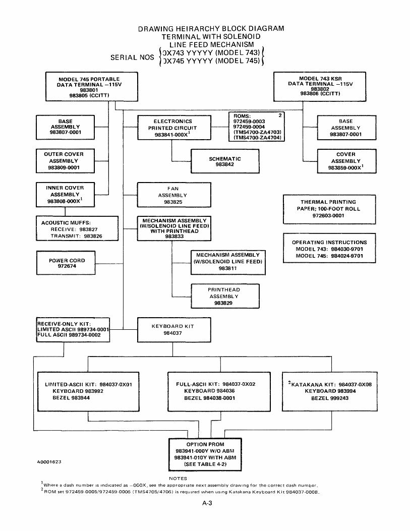
DRAWING HEIRARCHY BLOCK DIAGRAM TERMINAL WITH SOLENOID
LINE FEED MECHANISM SERIAL NOS 18X743 YYYYY (MODEL 743) l
)X745 YYYYY (MODE L 745) ~
MODEL 745 PORTABLE DATA TERMINAL -115V
983801 983805 (CCITT)
l ROMS: 2
BASE ELECTRONICS 972459-0003 ASSEMBLY ~ - PRINTED CIRCUIT -- 972459-0004 983807 -0001 983841-000X 1 (TMS4700-ZA4703)
(TMS4700-ZA4704)
OUTER COVER ASSEMBLY - SCHEMATIC
983809-0001 983842
INNER COVER FAN ASSEMBLY - - ASSEMBLY
983808-000X 1 983825
I ACOUSTIC MUFFS: MECHANISM ASSEMBLY
RECEIVE: 983827 r--(W/SOLENOID LINE FEED)
WITH PRiNTHEAD TRANSMIT: 983826 983833
MECHANISM ASSEMBLY POWER CORD (W/SOlENOID LINE FEED)
972674 983811
PRINTHEAD ASSEMBLY
983829
RECEIVE·ONl Y KIT: KEYBOARD KIT LIMITED ASCII 989734-0001
984037 FULL ASCII 989734-0002
I I I
LIMITED-ASCII KIT: 984037-0XOl FULL-ASCII KIT: 984037-0X02 KEYBOARD 983992 KEYBOARD 984036 BEZEL 983944 BEZEL 984038-0001
I
I I I OPTION PROM
983941-000Y WIO ABM 983941-010Y WITH ABM
AOOO1623 (SEE TABLE 4-2)
NOTES
MODEL 743 KSR DATA TERMINAL -115V
983802 983806 (CCITT)
BASE ~ ASSEMBLY
983807-0001
COVER '--- ASSEMBLY
983859-000X 1
THERMAL PRINTiNG PAPER; 100-FOOT ROLL
972603-0001
OPERATING INSTRUCTIONS MODEL 743: 984030-9701 MODEL 745: 984024-9701
I 2KATAKANA KIT: 984037-0X08
KEYBOARD 983994
BEZEL 999243
I
lWhere a dash number IS indicated as -OGOX, see the appropnate next assembly draWing for the correct dash number.
2 ROM set 972459-0005/972459-0006 (TMS4705/4706) is requ Ired when uSing Katakana Keyboard Kit 984037-0008.
A-3

DRAWING HEI RARCHY BLOCK DIAGRAM TERMINAL WITH STEPPING MOTOR
LINE FEED MECHANISM
SERIAL NOS {OX744 YYYYY (MODEL 743)} . OX746 YYYYY (MODE L 745)
MODEL 745 PORT ABLE MODEL 743 KSR DATA TERMINAL -115V DATA TERMINAL -115V
983801 983802 983805 (CCITT) 983806 (CCITT)
I BASE ELECTRONICS BASE
ASSEMBLY - fo-- PRINTED CIRCUIT - ASSEMBLY 983807 -0002 937300-000X 1 983807-0002
OUTER COVER 2ROM SCHEMATIC COVER
ASSEMBLY - fo-- 996522-0002 937299 ---- ASSEMBLY
983809-0001 (TMS4732-ZA3215) 2200044-000X 1
INNER COVER FAN THERMAL PRINTING ASSEMBLY - - ASSEMBLY
999239-000X 1 983825 PAPER; 100-FOOT ROLL
972603-0001
I MECHANISM ASSEMBLY ACOUSTIC MUFFS:
RECEIVE: 983827 - (W/STEPPING MOTOR LINE FEED) OPERATING INSTRUCTIONS
TRANSMIT: 983826 WITH PRINTHEAD MODEL 743: 984030-9701
999264-0001 MODEL 745: 984024-97Q1 KATAKANA MUFFS: RECEIVE W/STRAP
995671-0002 MECHANISM
OVERSIZE TRANSMIT ASSEMBLY
W/STRAP 995670-0002 (W/STEPPING MOTOR LINE FEED)
999257-0001
POWER CORD PRINTHEAD ASSEMBLY
996289-0002 983829
RECEIVE-ONLY KIT: KEYBOARD KIT
LIMITED ASCII 989734-0001 984037
FULL ASCII 989734-0002
LIMITED-ASCII KIT 984037-0X01: FULL-ASCII KIT 984037-0X02: 2KATAKANA KIT
984037-0X10: KEYBOARD 983992 KEYBOARD 984036 APL KIT 984037-0X20:
BEZEL 983944 BEZEL 984038-0001 KEYBOARD 999416 BEZEL 984038-0002
I 1 I r OPTION PROM
983941-00YY W 10 ABM
AOO01623 983941-01YY WITH ABM (SEE TABLE 4-2)
NOTES
IWhere a dash number is Indicated as -OOOX, see the appropriate next assembly drawing for the correct dash number.
2 ROM PIN 996522-0003 (TMS4732-ZA3213) is required when uSing Katakana Keyboard "'It 984037 -001 O.
A-4
KEYBOARD 983994 BEZEL 999243

D
e
A
• 7
116. ~:U~,,~:;'~I'U~ .. -:'D ; TIGHTOt 11) 1\~\1't la:. ..... 'II£TIHt.~n£~U 1\ 1"6111£1\10 3.S!:.:S IN-LeoS "I!\~ A~ ;;'~.L I I(EVBOlRO ANi) INSERT lIRE '1<IIfl. a:,tt. ON -0001 &,.., -000l. ONLY •
11. TlItlt SIOAU. Sf .(JIIl I.. Iii SAFETY CO\I£R liTEM t71 I'OSTlIUEO ON UWIT TI Ito! u..-... eN pWa ASS'" (ITEM l) OVER POWER 1E.EIIt TIl! ~!f IWSIIT SUPPLY ... tG~ IIO!.TA/C: AQEA. .....a ~f l£ t_ CIIH. 1-1-. M .. ~ illTlllEfN .lJln 1'18 :l1 sec 'NSf!!T
II. eMIIEIt UNITS 'SING I1fAlS 1M> , ... 1. ::a~~1? ~I\IIU 6£ C· O":} , ... 'fII THWII15 WCIl :ill/tAL 15.N,,""'I'[,..EENCOTHltil ~ .. ~t:f 'NTr:T NO jEII£~ <111' 745 myr; ~,~ fASl 5>0 .... bE 0.000'"
~/E~i,f1G:,~~'t}t~!t,; (NOTES ceNT SH /A)
6 IS
00 FOR -OOO/~'OOO3 ITEM 15" WILL 8£ MARKED pen 9 39231 -00/"3 !'""OR -00024-0004 ITEM 15 WII_L aE MARKED PCR 999Z3l-1l014
HI ATTACH 6ROUND CA&£ F"RDNI L3~' TO ITeM:5 H.IM TO IN!>TALLIN6 ITEM 1#
~"S.JRE J30\ Of ... ~c P-he ASS'" T£. 2}1!a \NS'T~~Di" @:F~1~~r~~~I~w~ ~':. ~~~Q~~i4f&"%Zi~':;,jN m Io.ITLCIIAL JUO/IPU PLU6S,ITEM 1I,IIl5'ALL£ll DfI·OOO I
AS!.ENIIII.'f ONL~ !] N'PL) IlEM 15 TO IION'TElTURtD I'IftEl'l.
III KEf" WIU'> 00"'1 OF rAN AND OFF MEAT!>INIC. WHEN 1.!lTALLINC;- ITEM c;..
PAR' NUM8ER
~83!!OI-OOOI
!I131OHUIIIZ
TOP '-'C,V I!II11N IIIltEIl COilE-it (ITEM &) , DllTEIl CDO'EIl (ITEM 7) __ ,,£0 RJIt t:LJftrlTr
~6cU. __ """"
~=--~=-~" .. - .... ~--. ~=-.. ~
rESeRIProM
DtIoTA TERMINAL 745 PORTA8LEJSTAl'I __ 'O_ARD __ H
OATA TERMINAL 74$ PORTABLE! J Iflft/ l.CPlR
DATA ITRMINI.L, 145 PORT, STANOAA:l,WlO "YBD
DATA TERMINAL, 745 PORT,W/AUX.CP!.R,W/C KY80
•
L _' /
-- _ l
... .. , .. ""----f""~·~m~~_n5~. ,383801' ~,&~,=,o~.====~~·!~m~rl5~!~m~i~·!~a~Il-~~~~~~~~~l-__ l-__________ -L~ ________ -l~~!I::~::~;l~:I~~-•
-.: .~'
'.8CI1I1
-ao ' ,.&,.M ~. ~.:.r.
D
-
c
B
-
A
e
"IOTES COIVT
/3 INSTALL ROM tlTrI,/38J I/T LOCATION VIO ON THE TEffAl./NAL fLfCT1i'ONICS (ITEM.?), SECURE WIT/.{ KTV IITEiIJ.3~)
[g ~~~l~E~O~~{;~~ NOT 70 .HOI ON
ZI. ERf?lIfR IINITS USED ITEMS "10 TtI,rV 45' IN PIAC[ or ITEMS 1,2,3,b.B,(.?7 flESI'ECTfIIELY IILL OF ITEUS 40 THRf) 45 M!lST BE !lSED TOGETHEf: ) FIIKTS liRE NOT IN7EKCH/INGElIlJLE:
I 7 I 6 I 5 j 4 I 3 121 '4
1
IR
D
-
c
B
A

o
c
8
A
1-::5::7 J=:=6 ~~~~ 1'i14k£F 5 l · g: 13 REf:
2
,,,n'm w ®V/ ~
20
SECT/ON 8-B seAL E' NON£: 4- PLACE 5 (2(0180· CW)
SHT 1 ZONt. c-"
'i
CAI3L£/JU'.WH PLUG HOO Dr_SCRIPTION K-UP SC.HEDULE
(ITE M 3) M,)TOK DKIV,,-~pp~1-~oe'--+-1~=-::~---L~~OrI tl (ITEM 3) HEllO liFT 5 peo,--- --_ .....
9 CiTE"" 3}lINE FEE ()L P2S1
(iTEM 3)SEN50R D MOTO~P2'2
.IEW L-[ $;.CRLE'N{JNE 5HT I ZO YE C-4-,.orATED 3~'' CW
o
c
B
o
A

LIST OF MATERIALS
Assembly Part No Rev
DATA TERMINAL, 745 PORTABLE, STANDARD, WIO KEYBOARD 0983801 0003 R 0983801 0004 R DATA TERMINAL, 745 PORTABLE, W/AUXILIARY COUPLER, WIO KEYBOARD
Item No,
0001
0002
0003
0005
0007
0009
0010
0011
0012
0014
0015
0015A
J016
0017
0018
0019
0020
0022
0023
0024
0025
0027
JOB
0035
0038
0039
0040
0040A
0041
0041A
0042
00424
0043
00434
0044
1)044A
0045
0045A
Quantity
00001.000 EA
00001.000 EA
00001.000 EA
00001.000 EA
00001.000 EA
00001.000
00003.000 EA
00003.000 EA
00003.000 EA
00004.000 EA
00001.000 EA
00001.000 EA
00004.000 EA
00002.000 EA
00002.000 EA
00004.000 EA
00001.000 EA
00001.0:)0 EA
REF FA
REf- EA
REF EA
00001.000 EA
00001.000 EA
RE:f- EA
00001.000 EA
AR TU
00000.000 EA
00000.000 EA
00000.000 EA
00000.000 EA
OOOOO.DOO EA
ODOOO.OOO EA
TI Part No. DeSCription
0983807-0002 BASE ASSY,743/745.RECT CONTACT P.R CONN
0937300-0001 TER~INAl ElECTRONICS.7431145 ~/~ODE~
0999264-0001 MECHANISM ASSY.STEPPER MOTOR, W/PRINTHO
0983825-0001 FAN ASSY
0999239-0001 COVER ASSY.INNER.7451165,W/XMIT ADJUST
0983809-0001 OUTER COVER ASSY
0983905-0001 ClIP,KEYBOARD,fRONT
0983904-0001 ClIP,KEYBOARD.REAR
0912487-0001 JuMPER PLUG,CONNECTOR BLACK
0983907-0001 SPACER.SPRING
0983863-0001 BRACKET,fAN MOTOR
0999231-0001 PLArE. IlJENTIF {CATION-BLANK
983903-1 CAN Bf USED AS AlT
0912988-0019 SCREW 4-40 X .150 PAN HEAD CRES
0912679-0009 SCREW _4-20 X 3/8"LG THO FORM,HEX
0411101-0057 lOCK~ASHER _ 4 EXTERNAL TOOTH CRES
0419346-0342 HELICAL COMPRESS SPRING
0983914-0001 ~AMEPLATE,OUTER COVER
0960141-0001 LABEl.SERVICE
0989481-9901 TEST PROCEUURE SIL 111 fiNAL TEST STA
0993816-9901 T~Sr PROCEDURE,RUN-IN 143/745
0984031-9901 TEST PROCtDURE,MANUAL 743/745
0937304-0001 COVER, SAFETY
0937322-0001 TERM ACCtSS KIT, 745 PORTABLE, STD
0984025-9701 MANUAL,MAINTENANCE,745/743
0996522-0002 lC.fMS4732NL-lA3215,4096 X 8-81T ROM
0417559-0001 SILICONE RUBBER IRTV) DOw 3140
0983801-0001 BASE ASSY,1431145.ROUND CUNTACT PWR CONN
USED ON EARLIER MODELS
0983841-0001 TERMINAL ELECTRONICS,745 w/ACOUSTIC CPLR
USED ON EARLIER MODELS
0983833-0001 MECHANISM ASSEMBLY wITH PRINTHEAD
USED ON EARLIER MODELS
0983808-0001 COVeR ASSV,WITH XMI lEVlL ADJUSTMENT
USED ON EARLIER MODELS
0972674-0001 CABLE ~18 Awe 3 COND PO~ER.[LECTRICAl
USED ON EARLIER MODELS
0983911-0001 COVtR,SAFfTY
uSED ON EARLIER MODELS
A-8
Remarks
for 00030nh

» cD
o
-
c
B
--
A
B \ 7
N)"':S (CC'T""~E:D ~R:;'~ ifeN£: x>-";) .. 'lAX ::~p 5c-'-.v£E". ~_ -=-'i' J:(J8 ~N .5 :Y£
'NS£""" ~V:;' !3~5E -,--= __ BE Gee IN 15 T>!ERE -,"ALL BE :::;0 ,N LIMIT ie
... ,tJ-ER~'- ..::,&p =E-,~ ~~N TI-I£ S =£ IN5ER- ":';:J ,5":5£ _-: \NCR CCVCR
'6 iliERE -,-~_L BE :::;: IN Llh'IT -0 i"H£ r;~:, ,,_ ~,.::= E~T.V£€N TJ..I£ 5 ~= I\S~"T .;a: 5A5£ C: \JNER '::C\.£1i
fl. EAJ;_J~Fi ..... • -~ t..,3:/V6 I-~·.I=':': TrRU.~ W£'i£ S~,;; 1_
I 6 1 rJ1'~S .:..c',"TUL..:.::-: Z.:'E >+
E] F:J.NER CCI;O .... tTE.tJ\ 8, =HIPPE~ L~IJ,;e:.
m t:."-:--l":1-0 J,.;..)\,: ... .J C~3 ... E: CR..)M £!~ '-0 IT&~l "3 ~\,);; TO I~STAL ...... I~"" IT\:::.M co
5J T.GH''""' .) to,.",> ''''- ,\!:. Q .... \G ...... -:-i: .... -'\.3:~ '5,~ l~~
::iESff; l~i __ ~j. -SJ.zRYls'" ;.;' =.is~.s y;yS;~~ 17£.1\1$ A~ .... 4',:: Z.7
UTI ~~:;it;;~ ['t:;~~~~ t·&[i~~cr;~~~h~-OOO2 -@'7~·[~32 ':.- ._.,. ~ .. .)
(W-=:'3 C:,,'T "'"'T2.) 13 MAl( GAP BETWEEN ouTrR RIB ON S,DC INSERT >'IND INNER ':OVER 5HIILL BE .060 IN.
(/oJOies; CONTNUE i!ONE D-8
TOP YIEW WITH II/HER r:aVF_~ (IrEN' £) f(E~DYED F[Jf CLANIT't'
4 I 3 I 2 I
~PA~R~l~N~U~Me~E~R~-------------DE~~~'~RI-PT~I·O~N-----------' ~
9832> OZ ·000 I O ... T ... TERMIN"'S i4! "~R, O:ZA /TTY
983602-000a OAT ... "TERMINAL, 743 K~R"w/MDDEM--
,}B3BDZ- 00C>3 O"'T/I, T[!1,NI\W~l 743 I(SR,E1~fTTY, 'tI/Cl K~BO
98380'2.-0004 DATA lE.RNlINI>.L 143 I\SR,W/MOOllol,W/O I\lSD

e
D
l
B
-
A
I 7
REF')q" I ~ :£,/' I
LJili
SE<:::TICAI A-A 5!:'A_E: F.JLL 5HT I Z~I\£ B-Et
SE.~'" ~ :.~ 5CI._~
2.
fl /
I
ROTA-E':: 9=~C"'"
I 6 I
EECTION .J-D SCALE: t4CI.E Z PLPCE 5 (I OPP05ITE. ftiO
IBO·CV'/ ) sur' Z;;J'£ 8-5
4 I 3
•
,cA8L£ HOO'(-UP SCHEDULE...
2 I
II, CNfZ?772 (C) fl I-').J._ t/J (He lIM -. a,n. 'I 11' ~ fij,j ~'/A: '~!I"I-oo .. ", (l., 2£{.£'''"£..- FPJM LfAlt -4 O,N' I Ir " .vA:
;_1_'" .,..J.-
p r J4ZZI€!C (I"~;"._~ ~UJ·2 Lh1,IT~-.Y' 2 /IAS 98.J!N·I-1 -;-,/ 77
DE5C.~/PTION START F/l1I5H UHlARKS
ITENI5 Fflrl A55Y P30Z. 1"11'.'8 - r302
~Z+-(-'T-E-M-3-)~PR-I-N-T-H-EA-D------P-I-OI--~~p-w~a~~7-'o~,-+r=i/~N=lH~[~~IN7(L-UO=E~D-W-I~--'~TE-M~3~
\ill 3 ITEM 4- KEYBOARD A55Y W(PI
ITEM b PONER CORD P3t'J1
uyaD -INIPI
.. tit) -T3')1 -
5" (ITEM 3) MQTOf? DRIVE P!!OI -T!!OI 'lCLUDt:D WIT),; ITEM 3 ~+-------,-------------------~-+------~ O~LIER MOCELl: USED LINE -, (ITE.M 3) HEAD LIFT 5'JL P2.!:1 -:ri?S: ':-~D ~LENOIC'
I; eLUDED WITI-I iTEM-~ ~:+-~~:~_;_: __ ;~:_:_:_'~_5:_:_E_D_A_ro_T_OR __ :_~_'_Z __ ~ ____ -_7 __ Z_S2.-4
t--='-,.+--IT:.....(-M-"--.. -UU-P-~-II-P-LV-'-G----P-WJj--_ E-~-13---+----.... -' E - J/ ~ UIII'~R PLUGS, ITEM Ib I NST~LLW f-'O+--'T.-'E-M-'-'-<1-U-""-P-l-Il--PL-lJ-'G---'-PIM-'l3---E-f-'S---+-n-,-,-8---£;-01-1-" ~ ~~, _y DOD t. c:-:x:JC4 ASSEMBLIES
VIEW [-C -SCI'lLE:NON£ SHr I ZONE :::-4-i<OTATED 901> C~·.
rDf96214r· ..... NO ~ 83 IS 0 Z-il_v A&> 3HEET :z.
D
c
A

LIST OF MATERIALS
Assembly Part No. Rev.
DATA TERMINAL, 743, KSR, EIA/TTY, W/O KYBD DATA TERMINAL, 743, KSR, W/MODEM, W/O KYBD
0983802·0003 0983802·0004
AE AE
Item No.
0001
0002
0002
0003
0005
0006
0009
0010
0011
0012
0014
0015
0015A
0016
0017
0018
0019
0022
0023
0::>24
0025
0032
0035
0036
0037
0038
0039
0040
0040A
0041
0041A
0042
0042A
0041
0041A
0042
01)42A
0043
0043A
0043
0043A
0044
Quantity
00001.000
0000 1.000
0000 1.000
00001.000
00001.000
00001.000
00003.000
00003.000
00002.000
00004.000
00001.000
00001.000
00004.000
00002.000
00002.000
00004.000
00001.000
REI-
REF
REF
RtF
RtF
:J0001.000
00001.000
00001.000
AR
000CO.OOO
00000.000
00000.000
00000.000
00000.000
00000.000
00000.000
00001.000
I:: A
EA
EA
EA
EA
I:: A
EA
EA
I:A
EA
EA
I:: A
EA
fA
fA
EA
EA
EA
EA
EA
EA
I:: A
EA
EA
EA
TU
EA
I:A
~A
EA
EA
EA
EA
EA
TI Part No. Description
0983807-0002 bASI:: ASSY,743/74S,RECT CONTACT PWR CONN
0937300-0002 T~RMINAl ElECTRONICS.743-EIA/TTY
0937300-0001 TERMINAL ELECTRONICS,743/745 WI MODEM
0999264-0001 MECHANISM ASSy,~TEPPER ~OTOR, W/PRINTHO
0983825-0001 FAN ASSY
2200044-0002 COVER ASSY,743/763,WITH XMIT ADJUST
0983905-0001 CLIP,KEYBOAKD,FRONT
0983904-0001 CLIP,KEYBOARD,REAR
0912481-0001 JUMPER PLUG,CONNECTOR BLACK
0983907-0001 SPACI:R,SPRING
09A3863-0001 BRACKET,FAN MOTOR
0999231-0001 PLATE, IDENTIFICATION-BLANK
983903-1 CAN BE USfD AS ALT
0972988-0019 SCREW 4-40 X .150 PAN HEAD CRES
0972h79-0009 SCREW j4-20 X 3/8"LG THO FORM,HEX
0411101-0057 LO~KWASHER j 4 EXTERNAL TOOTH CRES
0419346-0342 HELICAL COMPRESS SPRING
0960141-0001 LABEL,SERVICE
0989481-9901 TEST PROCEDURE SIL III FINAL TEST STA
0993816-9901 TEST PROCEDURE,RUN-IN 7431145
0984031-9901 TEST PROCEDURE,MANUAL 1431145
0983999-9901 143 CONTAINER,SHIPPING ASSY,PACKING SPEC
0984025-9701 MANUAL,MAINTENANCE,1451143
0931322-0002 TERM ACCESS KIT. 143 KSR, EIA/TTY
0931322-0003 TERM ACCESS KIT, 143 KSR, WI MODEM
0996522-0002 lC,TMS4132Nl-lA3215,4096 X 8-BIT ROM
0417559-0001 SILICONE RUBBE~ (kTV) DOW 3140
0983807-0001 BAS~ ASSY,7431145,ROUND CONTACT PWR CONN
U~ED ON EARLIER MODELS
0983841-0002 TERMINAL ELECTRONICS,743-EIA/TTY
USED ON EARLIER MODELS
0983833-0001 MECHANISM ASSEMBLY WITH PRINTHEAD
USED ON EARLIER MODELS
0983841-0004 TERMINAL ElECTRONICS.143/745 W/MODEM
USED UN EARLIER MODELS
0983833-0001 MECHANISM ASSEMBLY WITH PRINTHEAD
USEO ON EARLIER MODELS
0983859-0002 COVER ASSY,143.W/O TRANSMIT ADJUST
USED ON I:ARlIER MODELS
0983859-0001 COVER ASSY,143,WITH TRANSMIT ADJUST
USEO ON EARLIER MODELS
0937286-0001 lABEL,UL,7431145.7631165
A-11
Remarks
for·0004
for·0004
for·0004 only
for·0004 only
D
c
B
It.
B 7 6
c:::J~~H~~t~~!~.I~P~~~;~/'::.v x THnT THE BL/JOE I~ CEAJTU=~ 0-;r;.~~:;;~/=~T~~;~~~;~~'J:.Tt;5-;:':~':%:T~~:~~/~~i2w~98#037
~~ 5F:'=IFI5C ~V_·..:JAlFI6UC,..rl"::;'.J EH=~""":;IlD!,dlLE5 orDEr 0/'..':'..;E.= J~'=':::: -,..: PWI3 r55 v(TcY Z)/:; IAJ'j TAiLED /J.lrt=TI)/lJI1.J6 :u.DT~
: 'TFM~/t6 ~=FC~c 11u';Ti:L ..... 'J.J6 ITEN'J16 0t.v5TIII.L '-f,C·':hhTE(JTEMZ:J).:JllCl TEe .'::VU:(tTEM 7)1>5 5HOWAJ III wEW E
[IjIAlTFRUh_ u~H?Er PLJJS~ ~!TE/VII/)IAl5Th .. LED DM -01014. -010 3 J95~EM.eL Y' CULY
@]IiPPL~ ,-,="'"'5 TCIJ.JlJ-Tc"Tuf"=i)hl-:~'; 12]KcEP WIFE:: OLIT OF f'IW /JJJD DFF HEhT511J1( VYHEAll1tl5 TJ'lI.LlIJ6 ITEM6
o l'f.t ~~LLA1~:/::;t§t-!::Z~LM$: F"A' "';I'?Z Ai" P9 1 -IX3Z FCW "';1,)3 A. P£<' -tJtJ3C Faf' -()I':;"; ,,1_- PER -v"a53 ;:r:¥-P'/~AJ F£k _172.3/ F~ _':;It;.;u~~ .rEf 99!7Z.!I-OJ14
10 FEF
, 'StDR 1;7-~1 CJ6
~
8
TOP YIEW WITH/AiAIEr COIIEI. (iTEM6) , 0';7£r corEr (IUM 7)
I?EMOIIEO For t:lRC/7r
""""TOONAL
CLASSIFICATION
7 6
5
(!] .:;rTIlCH 6raL/lie Nl~lE FROM J301 TO
ITeM -' PRIOR TD 1J.J~rpLlIV6 IT£M6 [i£J Tl6HUli TO 8 ~ '5 W-1.8':;
@]TI6HUlI TO Z!.'5W-l8~
4
IZ M~"M.hI' t:A' 4'ETISE6tI ".liTER RIB P,(Iff'!): ILE-i'T ,-IULJ 4/~e,~' CP,:R -'Mil BE .P~"I,{/CHEj
13 AU%llfpA' M"' BETI:EE,u t/vTER A'a1 "U ,Ie: IUfEA'T ,-lULl ~.:E fAHi.L BE """lUCk:'>
1# THERE SH,-ILL BE 09.:7 /U~:S L/,}:/T Tt? LATE/(,I// ;;;::E:ETJYEE.tI T,j,:-.:'I.e: /UJ"ERT ,-IUP &-I.:E PR /,(/,v,:,R
15. TMSfE .. MLL LIE "9t7 /UCHEj t/41IT T" mE A'APML ~~::AETH'EEU TkE .:'IPE /UJ"ERTAUP MJE PA' hV.bEA'
5
3
F '7,I'7,Jfj:J.(!I;f!'. ~(/jALJPELlu,pTE; IZ'/~-77
eN 42'H43rf.1I1h.... fI) f!EVI~f.D
G -%~CJ} ;::~L~OIO(' TITL£.S,ONLM" 1-1,71
eN 42!H17t.; (DI J'L-..//J ()N 5H I, REVISED PICTORIAL PEP. DWG 9?J9ZS7f21AOOED NOTES" Ttlif 1'!:H31ADDED ITEMS 38 THRIJ -1!>
(4-1ADDED PLIlG WITH 'CORD GtrIP"
H !o~:,T~~U '-~/:~EL~~;,~:5~:;:~~T;
,.lIrr llLlM8EE
PrI CHIINGES Ib ION 5HZ, LIN£. :3 CF CABLE/JUMPER PLVG SCHEDIJLE,
L~~~~fll~/'r~r;il '1'o~;Dt':nV,/ft.~E~L, 5OLENOID"TO RfMARKS COL, LINES /I THRillS, ADDED ~OJ05"TO REMARKS COL
DESCt:IPTlOIJ
"8~B05-0IDJ OATR TERMIlIHL, 745, KATAKANA , W/O KYBD
"S360'5-CIOz. 011711 TEFMIA/IlL, 745, KANA, W!AII, CfUI, NI' KYBD
983805-0103 DIlTIl TERMWt9L, 745, CC ITT, WIO KYBD
983d0'5-0IC.'4 011711 TERMIIIIII., 74-5,(( ITT, W/AVI CPLR, W!D KYBD
98Ja05-Jl0~ OAT~,\ TERMINAL,74S, JAPAN t Hlo )(YB!)
9b_BDI5-0IQc. OArAT£NNtINAL J 745,JAPAIV, willI/X CPLR, wlo KYBD
c
B
It.

=!> ~
W
D
C
B
, A
8
/U~ Z Ur8(JIIfiJJ
.3 I't.ACES 9
Z5~.IZS
7
2CTIOU !l-A !lCR£E.I/' 5N 1(8-6)
6
Z REF rEYtJOALD IAJSEAlT
10 3pLAl"ES
Vlelll£ 0 lJUTEC CoIIEC/ITUn) wnN IIIUiIU'lHTC(ITEM zo)
5HI/.:-5)
~CTIOAI B-B 'CAlE:UOAlE
#NIlUS (Z II) 180" ,w) !lH I(C-6)
4
'Wf'LIOMDllISErT
ceY_ ~ReF
P ~z
SECTIOND-D XlII.e:AlD.UE ~ ~At'E5
"""AD5I re CliO 1t0TATED I.O·trt) :lII I~~
3 2
t!AIJL~' JUM"Er PLU& Mooe-up ~C/lEDUlE
DE5criPTIOAJ STllrT
(IT~M s) FAA! I/55Y P50Z
{ITEM 3} prlUTHERD 1'101
KEYtJOArD 115'1" WIl'l
# NIlEA' Co,fO,99r.ZLJ'-CJOOZJ P3D1
5 (ITEM 6) ,pEAKEr P#OI
II (FTEIf6) JIIIlcrOPHOAK P#OZ
7 (nEM 3) MOTor ~/YE 1'101
• ('/TEM 3) #l£ilD ~FT SOl.. 1'151 .. (tTUII 3) (III/! 'EED ,..,TO" pur
10 (ITEM 5) SEUSOK PI
II (FTEM II) ui.lMl¥K pt,,6 pIIIIIS-E.DI
11 (ITEM II) pHltJ-E#OZ
15 (lTENlII) PWIS-I!405
~'EF
IIIEW t.'-c 5C"l~:AlON~
5" I (C-#) I'tJT~T~D ""-I!W
FIAIISH
PW/J - ":~DZ.
PWll -.1101
f(YIlD - WIllI
P/IIItJ - .130'
- "401
-J#O~
-.110'
-.115'
-oJ15Z
PWI!J - .11
PWi!J -£.0_
p/IIIa - t'#05
_IS -£#06
D
C Iretllf"rK5
P"1I7111fAO IIKUlWD WITN ITEM 3
[z] Pf!fff1O:fit'''!!f".Wf''41C M/OIYEK
Y'6UEr III{LVOED WI;-II IUM"
MICI'OPfItw..c _LLlDCO WiTH ITFM6
IAlC!I.IDED W, TH
IT!!M :5 E,,*!LI£" MODEL.5 V$ED
"N~ 'Ull $DL~NOIQ
IAlUFAlIIL.JlJIIIP£r Pl.U65,ITEMIi IAl5 TAlit'D OAJ -0101, -o,c~ ;-0'05 ASSEAltJt I" OAil y II
A
LIST OF MATERIALS
Assembly DATA TERMINAL, 745, KATAKANA, WID KYBD
Part No. 0983805·0101 0983805·0102 0983805-0103 0983805-0104 0983805-0105 0983805-0106
Rev.
l l L L L l
DATA TERMINAL, 745, KANA, W/AUX CPlR, W/O KYBD DATA TERMINAL, 745, CCITT, W/O KYBD DATA TERMINAL, 745, CCITT, W/AUX CPlR, W/O KYBD DATA TERMINAL, 745, JAPAN, W/O KYBD DATA TERMINAL, 745, JAPAN, W/AUX CPlR, W/O KYBD
Item Quantity TI Part No. No.
Description
0001 00001.000
0002 00001.000
- 0002 00001.000
0005 00001.000
OOOb 00001.000
0006 00001.000
0007 00001.000
0009 00003.000
0010 00003.000
0011 00003.000
0012 00004.000
0014 00001.000
0015 00001.000
0015A
0016 00004.000
0011 00002.000
0018 00002.000
0019 00004.000
0020 00001.000
0022 0000 1.000
0027 REf
0028 REF
OOZq REF
0031 00001.000
0032 REF
0033 00001.000
0034 00001.000
0038 00001.000
0038 00001.000
0039 AR
0040 00000.000
0040A
0041 00000.000
0041 00000.000
0041A
0042 00000.000
0042A
0043 00000.000
0043 00000.000
0043A
0044 00000.000
0044A
0045 00000.000
0045A
EA
EA
EA
EA
EA
EA
EA
EA
EA
EA
EA
EA
EA
EA
EA
EA
EA
EA
EA
EA
EA
EA
EA
EA
EA
EA
I:: A
EA
TU
EA
EA
EA
EA
EA
EA
EA
EA
0983807-0002 BAS~ ASSY,743/745,RECT CONTACT PWR CONN
0937300-0004 TERMINAL ELEC.743/745 CC ITT MOD~ (NTTI
0937300-0003 TERMINAL ELECTRONICS.743/745 CC ITT MOUM
0983825-0001 fAN ASSY
09qQ23q-0004 COVER ASSy,INNER,745/76~,JAPAN
0999239-C003 COVER ASSY,INNER,745/765,W/O X~IT ADJUST
0983809-0001 OUTER COVER ASSY
0983q05-0001 CLIP,KEYBOARD,fRONT
0983904-0001 CLIP,KEYBOARO,REAR
0972487-0001 JUMPER PlUG,CONNECTOR BLACK
0983907-0001 SPACER,SPRING
0983863-0001 BRACKET,FAN MOTOR
0999231-0001 PLATE, IDENTIFICATION-BLANK
98390S-1 CAN BE USED AS ALT
0972QSS-001Q SCREW 4-40 X .750 PAN HEAD CRES
OQ72679-0009 SCRE~ #4-20 X 3/8"LG THO fORM,HEX
0411101-0051 LOCKWASHER N 4 EXTERNAL TOOTH CRES
0419346-0342 HELICAL COMPRESS SPRING
0983Q14-0001 NAMEPLATE,OUTER COVER
0960141-0001 LABEL,SERVICE
0984026-Q901 TEST PRCC,SYSTEM TEST,743/745
098387b-9901 TEST PROCEDUPE,RUN-IN
0984031-QQOl TEST PROCEDURE,MANUAL 743/745
OQ37304-0001 COVER, SAfETY
098400Q-9901 745 CONTAINER,SHIPPIN& ASSY,PACKING SPEC
0984025-9701 MANUAL,MAINTENANLE,745/743
OQ37322-0007 TERM ACCESS KIT, 745 W/O KYBD,KATAKANA
0996522-0002 IC,TMS4732NL-lA321~,4096 B-BIT ROM
0996522-0003 [C,TMS473ZNL-lA3213,4096 X 8-BIT ROM
0417~59-0001 SILICONE RUBBEk (RTV) DOW 3140
0983801-0001 BASE ASSY,743/745,ROUND CONTACT PWR CONN
USED ON EARLIER MPOELS
OQ83841-0003 TERMINAL ELECT 743/745 CC ITT MODEM
0983841-0005 TERM ELElT 743/745 CC I1T MUDEM (JAPAN)
USED ON EARLIER MODELS
0983B33-0001 MECHANISM ASSEMBLY WiTH PRINTHEAD
USED ON EARLIER MOOELS
0983808-0004 COVER ASSY,INNEk,745 JAPANESE
0983808-0003 COVER ASSY,w/O TRANSMIT LEVEL AOJUST~ENT
USED ON EARLIER MODELS
OQ72674-0001 CABLE NlS AwG 3 COND POWER,ELECTRICAL
USED ON EARLIEk MODELS
0983911-0001 COVER,SAfETY
USED ON EARLIER MODELS
A-14
Remarks
for-0101,·0102,·0105,-1016
fo,-0103,-0104
fo,·0101,·0102,·0105,·0106
fo,·0103,·0104
fo,·0101,-0103,-0105 only
for-0103,·0104,·0105,-0106
fo,·0101,-0102
fo,-0103,·0105,-0106
fo,·0101,0102
fo,-0101,-0105,0106
fo,·0103,·0104

o
-
c
B
-
A
8 7
0~~S~{~!:;';}2f~E::~}~;:~:: ~;;;;;T~~:£:;~f;:g 7H_C -=ItE -'=Y':'
GJ '..~..Jr~ I~':-I:;~ T"_: Pr.E ~~'5Y{!T~M Z)'51L:;'-.. _~~ 'L FETt4'J.jIL6
~ ~,~;~:,.':~-~::~:;~~{~:;~~~-::/;:;;~':c6;~-~~ ~~. _ ~:)4 to: _ :'._,
G ,.:.--: I' 4.-'=~ ::_ -::. ~ r~L' ';L:; JFFOF NeI1T~/LK AII':IJ ,(..:s .... ~ .. _Il.Jt:; '-ENE o F: ~ -, ~ -:, .. = 1/_ f£ ,'n. ~EO PE.(I q'992-Z -5~~
.:F..,""'r-:=t-lfe - ....... ---..: ... Cfr"f- ~-
c_-- . . -_/-: ,;- 1_,-'=3,1/F~c£PE!(79"':3-/.;_z-
o ,-: v:; _~/." -.:': ,.;(.-_: ~-'L_'rCliAL M#lCJ<IIlJE C? - ...: ,_:; ;;_r~ 1:1 T
Cli~ ~=l'::'= -,;~ ~:;~_-'F:~ -=-'_ CDJ.iFI6UrNTCA/.!J.C':T #1A10 5.JlE~'::'.'-DCL
o ;~-,.; -..=.. -';_I..D _~he.L Ff:;r J301 TO ITE/'A~ F£,:;.i' TO Ill5T-4Lt.lh£ ITEMS
~ T :~~.:!.. -:-:. 5$ ~/'--L&~
6 J 5 ! VOTES fttNTI!IJtO)
)t) MAl GA? 8=T//:E'1 CtlTEI? Rill !:1f5t:E INSERT ANlJ I ~E" a;YEk. SIfA.:{ if'; .C<':J IN.
/I. MAX CAP iE~ .t£EV (,tiTER RIB C'/ :/~ INSERT h 'f'; fA5£ 5ifALL BE cue IN.
/Z THERE S~A •• iIE tJ9C //I L//I1IT TO lliTERAl SA? i!E - kEEl, THE 51£)£ INSERT /iNO B/iSe IJR 1'.'11£,(" CC.JFil
IJ TI/ERE S).AtL BE ~ iN LIA:IT Tt: THE RAP/At. Gil? i'E TilED, TNE 51PE INSEA'T A VI) /TME tJR INNE;? CC.lEI!
,./ '="''''_ .,;~- vL : ti ... //.."; ITEI:- ~J ,.7~,,-# "E~E SERJ.lt. Ull ':E';/E': .,,"( 7<13 y~"vr.. tlU/T..;" //...'l.!.'; lTCI'': 1,::,3 ':,\,.;J (# ~~.:- ':£.'/~4- .tv :~£.:- 1),< 7U YYYrr'
15 "L '";<'_ .... ';1 ',7A'M;ATL~U/:vk V/./ct T;"E ~""E)'A1P...A.t. cL=-.. //..A" :$, /"7,1' ~)/";ECL/AE ,11Th T"t"'S+' 59)
I. EA,.,,-,.. ':1'1- td/,T V.:Eb ITE/,j-~?h/.I"'~ ! FJ:E tJF/7FA'~ t;:',J,4': t:I Ir'=;-~.:-_·TlcLY ALL 5.F /i?'~ WT/i'1/ ff"" "'vIr s: 11':£':; TZJGEr,t,.£~, BUT.: ArE ~~T .6TEA'C/(A,vGE/,SLE
o T.5tth-~-L T~ .3.5~SIl..._e:
0~w-o 118 \ 11 ~\ [,]0-~)J ~ "~'TII-0
I~?n fj~ 1\
0~ ~:I~~~~il l:-;-----/7-
~r.:/.t..:H'L 1J,Jj££T /I..J 5!1 Z/C-7j
9 REF TDP .. lEW
/AlliER CO;££ (lTc"M 6)
FEYlGYcD FcrCLAFITY
~~Q 1 ClAS SIF Ie L - ::", "-~I
S I 7 I 6 I 5 t
4 I 3
rfl E V S TAT U :; l-'R"~E",,V,=-_'=t-"'J'O-i OF SHEETS SHEET
T7~)· ~ 1">0 ~ T~> 001 T>">...(.L 'J ~"'? ~ .... ~; ''-L
4 .?o I 3
I , I
E ,Cn4-,,:o '[ ; /t)}/~ _
INI,'" J',' ')~"( -' ~'. ,~-THE FJLL"';'N,,'/; I-~ - ) ~;-!-LJ:~TIO'~/j)_:'1 ',_ '- "_,, ,Tn" 5 PI dJ.: ~;~, ~-: : : - 01 -102 : - 04 L"" - _ '" i:' - _ " :" .;, -/":; /'- ')2 - _.; H t.; .. I
C.u~Z¢5Z9/LJ)fP-"""- ./:...&'-'- {4fr IJELET£fJ /T~,;_ a,z" ~ _ ;=~ET£O
I ,'ff#.?~CIU-.//./'!./-/.4 J,~..",C,£-.:J
F 1:~;~:~~;/./~;-:-.' .!~//<:J~~: 999Z.JI-~v3:",./!; -':;/~ !y //Eh' 15 ;YAS ~99Z31-.//]"",?-I{/-c.1:'4. {J/ /TEAf 15 JII.4.f" 9;1~?3/-C..:/.!7" "" /,/./"-E ~ n"AJ -J
{5 ::;;;;::;;2:::(~:~~;~~£~~~ j-- --1-'-----1 NtJTES/{))II,IZA//:;;~ 1[-,,,-77 ~/r::-""_
.10_ -"'7,VJ'~A,£IA/TT/JN'9 K(P,:;
t--.-,......,C~>~,..,-:--oKl-::-~<!c-:-t-=-=--=-k-:'u==---·-.~-_-",.~=,~-~'v/'='7'er -
98J.8'JCD OIO~ CATA T£FI',' I'/~_, ;;?,.:c.. I - T I W / MCLEM
·~.fi-= '/','t'r ::'"..-~ ~:~/:~~;/:~/:~:'~;;~~~" I
I. _1- "-'...1-'
I' Z.
\ 2 \ I fllltU!
o
B
A

o
C
~ .... 0')
B
A
8 7
5ECTJDAI /l-A :J.."FlLE: 1/1 5" I{B-o)
6 5
~ECTIOU B-B seR£E: IJOUE
.PlRCcS (Ztii>/SO'CIIII) SH I (C-6)
4
U~FTKErlJORLD
~EEF
EEF 6 KEY13011F.
SECT/aU D-D seR£E:AJOUE
Z Ft:«ES (I OI'POSt U £LD /Bd CIO') 5» I{S-S)
3 2
CRi!JLE HOOK-UP 5CII~DUt.~ J DE5C~/PT/OAJ 5TAFT FI,u,='H
(ITEMS) FIJA/ p~,jr P30Z PWd-J30Z"
z (ITEM.3) PRIJ..JTHEjlO Pial PFII.ITHE.I9l> IAJCLLJDEO W,TIIITEM 3 --I:EY130R~O "'~5r W/PI KY8D - j/~/P J 1 --- .-"
S (ITEM 3) .MOTOF D.FI¥£ PZOI p"a - JZ:)I J 6 (ITEM 3) HEROlJFT SO£ PZ':iJ -JZ';;I !
'MC!.UD£C WITH ITEM 3 7 (ITEM 3) LWE FEED MOT()P Pz,z.
8 (ITEM 3) 5EA-SOC
I -=AALIER tHoPELS V.fE!J L.IA/£ 1-+'------------"-1If--t---- FEEO S()LEI./()I/J
-,.//
-JZ!Z
9 (ITEM II) JVMPE£ PlV,.
10 (ITEM II) dUMIEC pltla
VIEW c-e ~CI1LE:IJOAJE
5»I{C-~)
l£OTATED 90" C'N)
~W~-£4/~
PWB-E_,S
REF
_ £,e/"
PWB - e~/6
JUNlP£K PLV6'SIIT£M I~ 11I5TI1LL£D
OA/-OJOZ AIID -OO~ AS55f'3£1E,
o
c
B
o
A

LIST OF MATERIALS
Assembly Part No. Rev.
DATA TERMINAL, 743, KANA, EIA/TTY, W/O KYBD DATA TERMINAL, 743, CCITT, W/MODEM
0983806·0101 0983806·0104
Item No.
0001
0002
0002
0003
0005
0006
0008
0009
0010
0011
0012
0014
0015
0015A
0016
0017
0018
0019
0022
0025
0026
0327
0030
0031
0032
0033
003A
0039
0040
0040A
0041
0041A
0041
0041A
0042
0042A
004.3
00'.3A
Quantity
00001.000
00001.000
00001.000
00001.000
00001.000
00001.000
00001.000
~0003.000
00003.000
00002.000
1)0004.000
00001.00f}
00001.000
00004.000
00002.000
00002.000
00004.000
00001.000
REF
RfF
REF
RE:~
00001.0UO
00001. 000
00001.000
AR
00000.000
OOJOJ.LO,)
00000.000
aoooo.oOO
00000.000
EA
EA
EA
EA
EA
EA
EA
EA
EA
EA
EA
EA
EA
EA
EA
EA
Ef.
Ell
E:A
EA
EA
EA
EA
£A
[A
EA
TU
EA
EA
EA
fA
E:A
TI Part No. DeSCriptIon
09B3B07-0002 BASE ASSY,743/745,RECT LnNTACT PWR CONN
0937300-0002 TERMINAL ELECTRONICS,743-EIA/TTY
0937300-0003 TERMINAL ELECTRONICS,743/745 CC ITT MODM
0999264-0001 MECHANISM ASSY,STEPPER MOTUR, w/PRINTHO
0983825-0001 FAN ASSY
2200044-0001 COVER ASSY,743/763,W/O XMIT ADJUST
0996289-0002 CORO SET~3-PIN PWR-OOMESTIL GRAY W/CLIP
0983905-0001 CLIP, KEYBOARD, FRONT
0983904-0001 CLIP,KEYBOARD,REAR
0972487-0001 JUMPER PLUG, CONNECTOR BLACK
0983907-0001 SPACER,SPRING
09B3R63-0001 BRACKET,FAN MOTOR
0999231-0001 PLATE, IDENTIFICATION-BLANK
983908-1 CAN BE USED AS ALT
0972988-0019 SCREW 4-40 X .750 PAN HEAD CRES
0972679-0009 SCREW N4-20 X 3/B"LG THO FORM,HEX
0411101-0057 lUCKWASHER # 4 EXTERNAL TOOTH CRES
0419346-0342 HELICAL CeMPRESS SPRING
0960141-0001 LABEL,SERVICE
0984026-9901 TEST PRQC,SYSTEM TEST,743/745
0993R76-9901 TEST PRUCEOURE,RUN-IN 743/745
0984031-99Jl TEST PROCEDURE,MANUAL 743/745
0983999-9901 743 CUNTAINER,SHIPPING ASSY,PACKING SPEC
0984025-9701 ~ANUAL ,MA! NTENANCE, 745/743
0937322-0008 TERM ACCESS KIT, 743 win KYPD, EIAITTY
0937322-0009 TERM ACCESS KIT, 743 WID KYSD, W/~ODEM
0996522-0002 lC,T~S4732NL-ZA3215,4096 X 8-BIT ROM
0417559-0001 SILICONE RUBBER IRTVI DOW 3140
0983807-0001 bASE AS~y,743/745,ROUND CONTACT PWR CONN
USEn ON EARLIER ~UOELS
OSE3841-C006 TERMINAL ElFCTRONICS,743,FIA/TTY (JAPAN)
USED ON EAfil IE:R MIlDI::LS
J983841-0003 TERMINAL ELECT 743/745 CC ITT MODEM
USEJ ON EARLlER ~OOELS
0983833-0001 MECHANISM ASSEMBLY WITH PRINTHEAD
USED O~ EARLIER M00ELS
0983859-0002 COVER ASSY.143.W/O TRANSMIT ADJUST
USED ON EARLIER MODELS
A-17
M M
Remarks
fo,·0101
fo,·0104
fo,·0104 only
fo,·0104 only
fo,-0101
fo,-0104

o
c
:J> -00
B
A
NOTES UNLESS GTHERVI1SE SPECIfIED
lTI INSTALL 1l"EM' TO ITEM 2 f5CING CAREFULL 7D ALIGN P~OPERL Y WITH MOLDED-IN ALIGNMENT PINS USING EXlSTING HARDWARE
[!] DRESS CABLE AND CUP IN f. .JSITION WITH EX/STIN6 CLIP
SCQ IDENT
2
a. ON FIELD 5E~VIC£ LlAiITS AAJD gA~E'S JAlS7ALL PEA" .,. OAI P.A~E~ Pt£FLGC7Z),f! 7rJ C()VO? AssE/tIII1L'r AlUN1"E'~. JTEM 4 SN""lL t:'auTAI,u P/,u 9!1!!J~$7-lIoal M/O TNF AH.i'o,l'A?IATE" ,l'EV/SlCJA/ L £TTE'k? ~ "THAT PAKT NUMBER
3
PART OR IDENTIFYING NUMBER
~---+-----1;:~~~~§~~~E~2.:~O : ~2~~':'~~~: ~~~~0:~·::1~:~£~~:s
o.o<"Af H 1.~""'~o( E
NO PROCESS CLASSIF,CATION ~Ec,<E<'" _ F()R COR.-lELA" )/'.t TO (".O.lT I~O SPEC fICAT,r,I'\IC; .... fE TI CRAil o."t;-=;-:-........ --I
4 3 30 2
4
REVISIONS
~ N"+2f2St(C)-U? ~ TUM 3 PIN WAS Z2000+3
.R'~ .5
--:1f(J/ ",Z1-11 0.14[9334' D) 6. 7f1u:JItJ:&.., Cd 0
8 ADDEO J7EM 4 7lJ LM (2)AOD- I-Ill -71 /2Pt £1) NOTE .3
C CN-I2.12"~/EJ..s:IA>." .. JIJ ANJT£ J ,f.,LA WRS ... Pl'N99SlISN't)()/ ... 2-11-78
02
c

LIST OF MATERIALS
Assembly Part No. Rev.
MECHANISM ASSY, STEPPER MOTOR, W/PRINTHEAD 0999264·0001 C
Item Quantity No.
TI Part No. Description Remarks
0001 OOOOl.00C EA QQ83R29-0001 PRINTHEAU ASSY
0002 00001.000 EA Oq992~7-0001 MECHANISM ASSY-BMC FRAME
0003 R !:f t:A 0993609-9901 FUNCTIONAL TEST P~OCEOURE
0004 AR ~H 0232208-3500 LABEL WIRE MARKER OATABS VINYL CLOTH
A-19

a 7
NOTES: UNLESS Oll1ERWISE SPECIFIED m AFTER ,'1£ CARRIAC.E AS~EMBLY (lnM 4) IS INSTalLED ON TIlE CARRIA6E ROD = I~) P~:~ ~T D~~M~~ 'i:~rn TM£ "E" RIN6 ON T\.lE CARRIAGE AND Ott[ DROP ON EACII SIDE O~ TIlE CARRIA6E. MOVE THE CARRIAc.E OVER
e
rn INSUR£ T~AT DANCER SPRINC. IS NOT WARP£D OR PRELOADED. (A NORMAL LOAD APPLIrD TO T\.l£ CENTER OF THE "OUER SMOULD MEASURE 1012 01 WREN DAI.CER ROLLER BOTIOMS ON MEClIAlUW FRAME
D "T\E. OIL SEVERAL TIMES TO WET TI£ 'FELT WIPES INSIDE
I!I CLAMP CABLE ~M 24) ONTO CARRIN.£ ASSEMBlY OTEM 4) SO TWAT WHEN MOTOR ASSEMBlY (ITEM37)IS ENERC.leED IN PIIASE ",." (IE: VOLTAC.E 15 APPLIED TO BROWN AND BLlICK MOTOP WIRES) A GAP OF .08 ... 00/-.05 EXISTS BETWEEN THE SEATED BUMPER (ITEM 14) AhD TilE LE~ END OF TJ.lE CARRIAGE. TIIERE MUST ALSO BE TWO TURRS t"'~ OF CABLE ON FRONT OF TIlE CAPSTAN 0/1 TIlE MOTOR ASSEMBLY
l1J DISTANCE BETWEEN TOP OF BAIL (ITEM 20) AND TOP OF CARRIACoE WHEEL SIIAlL
c
B
III 1IMOVE PlUNC.ER FROM SOLENOID (lTEN$ jUlD INSTAll ''0. Rim (ITEM 53) ON PUo-w.ER, PLACE ONE DROP OF OIL (ITEM 30) ON PlUNC.£R BEFORE REPlACING.. MCIJf1 SOL£NOID TO BRACMET (InM 41)
DJ INSTAlL WA~IIE:R5 ~TEM 23) AND BEA"Itl6 RETAil'tER (lTEM ~~) ON SWl~T OF PAPER
~~ :O~~~O(I~~~L~~\~:~\S~ ,,¥~~y A .DIO:t.005 6AP EXISTS BETWEEN TilE TIIRIIST WASllER (ITEM z ... ) AND TilE SURfACE OF THE MECNANISM !'RAMi
~ TORQUe SCREW TO •• 01.!i I~S
4.. INSTALL SCREN (mM 310) t MWST SOlENOID ASSI;:I\IlLY 50 TIIAT PI'IIOT AND BAU ARE FREE TIIRDU/,MOUT TRAVEL OF PLIJIC.ER. TORQU£ SCREW TO loo.D!.!> IttUs
BE .O!i!U .OW
!!II ~:~KL W!"5ll!~1! N~~iS~Ndlt~W~ t~p~!ffrTE I/ItJ 221JOD:1/J
'- ASSEM'BI..£ SOLENOID 4 BRACKE! SUBASSEMBLY (vIEW ~ USING. PUSHON RETAINER (ITEM 38)
1'0. AlW5T SCREW UNTIL FORtE "J:" IS WITHIN TOLERANCE SPECIi:IEO. TillS MUST BE ADJUSTED WIIll.£ MAINTAININ6 ADJUSTMENT NO. S CON~TANT •
.m5~:&'1'k-1~ Il£ADLiH DIM-I
'1. IN5TAll DRIVE :'INK (lTEM04:1)AND AD.1UST 1]~=§~~~~~~8~ !&:AD LIFT TO D:MEN510N SHOWN BY AD.IUSTINC. SOLENOID DRIVE BAIl. OM SOLENOID PLUNGER
VIEW 0 SH2(B-2)
I. ASSEMBlE PIVOT (ITEM 4Z) ONTO ~RAME WITH PUSHON RETAINER (ITEM '38). APPLY I DROP OF OIL (lnM 30) TO BEARIN6 SURFACE.
2. ASSE",'8LE SOLENOID DRIVE BAlL OlE!'..' 43) ONTO !>CLENOID PUJN6ER :):1.1 TURNS. APPLY
~~i ~..?R~~1~Ni~~F~~EO~I~y6ALL/
.au!:: ~:!m ~!f.m
4f!::t ~!&AY ~!&\f
3
c
B
1-=:OOfKfH
999257 .-. IOF
LM

o
c
B
A
8 7
SECTION A-A
VIEW C SCALE: NONE
(A-5)
Z. PLACE CAIllE (ITEM Z4) IN SlOT AND WRAP CCW f.-lit TURN!'.
1_ PLACE TIN510N ARM (ITEM a) IN CATCH ;>O,IT ION
S. 5UlWLY l!n£ASE lEHSiON ARM fliDM CATCH POSITION
Go. I14TATE MOlOR CAPSTAN FROM ON£ EXTREME TO THt OTHER TO REMOVE AU.. SLACK IN CABLE
6 4
Il
3
,SEE VIEW 0 SH I (8-6)
2
VIEW B-B (C-I)
~
o
c
II
c
A

Assembly
MECHANISM ASSY -BMC FRAME
Item No.
0001
0002
0003
0001t
0005
0006
001)1
0008
OOOG
0010
0011
0013
0014
0015
0016
0011
0018
0019
0~20
0021
0023
0014
O~25
0027
11028
0029
0030
0031
00 32
01133
0034
0035
0036
0"31
0038
v"41
0042
"043
Quantity
00001 .• 000
00001.000
00001.000
00001.000
00001.000
J0001.000
00001.000
00001.000
00001.000
00001.000
00001.000
00001.000
00001.000
00002.000
110001.000
110002.000
J0001.0110
1l0002.JOO
00001.000
IlOOOl.000
00002.000
00002.000
JOOul.Oull
00005.000
00008.000
J0001.000
AR
AR
00C01.000
00007.000
JOOu 1.0011
JQlllll.JOO
00001.000
JOOOl.OOO
J0002.1100
000Ul.000
JOOOl.JOO
00001.000
00001.000
fA
fA
EA
EA
fA
fA
EA
fA
EA
fA
EA
fA
fA
EA
EA
EA
EA
EA
EA
EA
EA
fA
EA
EA
EA
EA
EA
TU
EA
EA
EA
EA
EA
EA
EA
EA
tA
EA
EA
LIST OF MATERIALS
Part No. Rev.
0999257'()()()1 F
TI Part No.
0999241-0001 FRAME, MECHINISM PMT
0983812-0002 ~OTOR,DRIVE-PRINTER
0983816-0001 SOLENOIO,PRINTHEAD
0983811-0001 CARRIAGE ASSY,PRINTHEAD
0983818-0001 ~INDOW ASSV
0983873-0001 SPRING,OANCER
2200030-0001 CEFLECTOR,PAPER
0983880-0001 ARM ,PUllEY-TENSION
0983883-0002 SPACER, PUlLEY- PMT
0959402-0001 PULlEY,CA8lE
0999258-0001 SPRING,CABlE TENSION
0999263-0001 ROLlER,PAPER DRIVE
0112684-0005 BEARINGS,SLEEVE-FlANGED NYLON 02510 10
0244440-0003 BUMPER,.500 0.0.
0983872-0001 ROlLER,DANCER
.)983874-0001 PIVOT
2200031-0001 SPRING,HEAD LIFT (STEPPER)
0983889-0001 BEARING,ROD SUPPORT
uqS3€84-0COI POD,CARRIAGE
1l983e86-0001 BPACKfT,BAIl
0983938-0001 BAIL RETAINER
0912485-0001 \ojA SHER ,S TEEl-THR US T
0959297-0002 CABLE,DRIVE- PMT
11983900-0001 KNOB,PLUNGER
0416622-0011 WAS HE R # 4 FLAT
J411104-0135 \ojASHEP ~4 LOCKSPLIT
0999246-0001 PAD,FRICTION
u232513-00J1 ell 1/43 TERREST IC
0232334-6050 LUBRICANT SILICONE GRS LT GR 2 Ol TUBE
0983916-0001 SPRING,EXTENSIoN
0972988-0015 SCREW 4-40 X .375 PAN HEAD CPES
u98G71l-0002 LA6El,WARNING,743/745
2200032-UOOI BEARING,RETAINER
u972969-0003 SCREW 4-24 X 1/2 HEX WASHER HEAD
L21l0045-0001 ~OTOR ASSEMBLY, 4 PH. STEPPER
J97L491-0023 RING,RETAJNING
220~033-000l PUlLEY,30T TIMING BELT
2200041-0001 BRACKET,SOLENOID AOJUST
2200034-(001 PIVOT ARM,SOlENoID
22U0035-0001 BALL,SolENOIO DRIVE
A-22
Remarks

LIST OF MATERIALS
Assembly Part No. Rev. MECHANISM ASSY-BMC FRAME 0999257·0001 F
Item Quantity TI Part No. Description Remarks No.
~044 00002.000 EA 0912988-0012 SCREW 4-40 X .188 PAN HEAD (RES
0045 JuJ01.01l0 EA 220()037-0001 OR I liE LlNK,BAll
JI.I46 JOOO1.IlJO EA 2200038-0001 BAll lINK,BAll DRIVE
0048 00001.000 fA 0537711-0005 Ot<IVE BElT
01l4S 00001.000 EA 0996624-0,,01 S(PEW,PLASTll E
0050 1.10002.000 EA 0972831-0002 PIVET.1/8X.195,TU8ULAR,STEEl,8LINO
0051 00OOl.01l0 EA 0912990-0017 SCREW 4- 40 X • 62 5 FL T HEAD CRE'S
0052 0001.11.000 EA 0416453-0021 t-IUT, PLAIN ,4-40 UNC-28 HEX,CRES, SMALL
0053 1.10001.0..10 EA 0983969-0001 a-RING
0055 00001.000 EA 0983968-0001 liAS HER RUBBER 1/32 THK GRAY
0056 AR EA 0802149-0222 ADHESIVE,THREAD SEALING AND LOCK ING
01)57 JOO01.1l00 EA 0983915-0001 IIASHER,SHOULDER SPRING
0058 00001.000 EA 0972112-0C03 TERMINAL .187"WO QDI SC TAB STYLE
0059 00001.000 EA 2200061-0001 CABLE, HOTOR GROUND
0061 00001.000 EA 2200061-0002 CABLE, MOTOR GROUND
0062 00001.000 EA 0411027-0803 WASHER, .125 X .250 X, .022 FLAT
A-23

e 7 6
o
5 N01f5 .• -~APPlY~ TEM S TO ScREWHEAD ON SENSOR
ADJUSTMENT AF1ER TEST
4 3
[~l)~~~~\~~J~~r?xt:~~~t~:~:~r:i:~~-,"~~;~'~~ "E:l>.tI PeA-:-:' HOLES.
~ PO'S\TIO~ At,D ~lTAC.rt f'-;::)\L\T--iE.J\C, !:'::." CABLE U5INC,
~~~ F(Ox~~r~ ~;;~~~~~S:(~l~:/;\.;'I ;::.~E.J'i~\~ r":~17Mr. 00 :AUT 'ON: PRlrn~:J:' "'5S~ ("eM Ii I~ VE~'
FRAGILE. E.X''':R:>.AE Cb,;.::'tJ=-\ e.: fAI1Et't TO F\VOI\:l CiA {i"GE.
[B At)JUSi KNOB 5.0 lr "1 5.~~£."i~lll) \-u-\:, A ST~o\\~ OF .045:1:.005 MF.AScQ~") ;..- I-1Ai,"JM D~"LEc.TIO/J. l'>I>.IL I'IA'f HAVE t.JO V,~.~ T~"'IJ .CJ'LO WAI.P W,T~IN O>JE LI'-lo LEIJ&iH.
2
__ -1 ____ ---
,r ';7"~J~:" ~'
3.)'.-I£X: :/':'::'1...,::,::;' :'_:'_'i=:' d~?: =- .... __ I"'~
~ <'3J-4[[ 1 1 f_ ~~- i,-c=I--:--:rl L'I'I'. IDtED liEii.:, 314-CH~N(,tD NOTE a ~JV;:;' ""~LJST JB:C, T n SOL~i~O ') H~C; A. :,TPOKE CI=" C"!O! w~.
4,:3 14 r..) .-"/...!"",/o -L2:~~/~L'J. t-.JOTt. 4 NA~·- -- 5TRJKE ')F ... :>~ MA,.( .::':'=- ' , J tI/·j,) ""'J;~ -;- ... A'J ;2J /I':;{ Ij-I-,~)'J h 'ilJ ."£ _ E _ --
o ;"21(;.2i:(CM~~/~,uij;Elf::7EOITEMr7"~--"'-: ~-4- reMOVED ITnoil 5 TO LM ANt) FD fj}IICtJElJ IMTE ~
C 6 4Z~Z-;~I'C)-J /fI.'/'J'..tt.{I)AO:.:;O~"1'l/ ... ,7"''' j.=-;:-:-=-4,3 II~ SCfI£IJUL' rz) AC!?£/J -8C¥)1 tM --
o
c c
B
%' [JOO EXISTING CARRI.o.GE !>(.REW
a PL~C.ES C.ABLE R£:TAlltlN> CUP
ORIVE ASS'! t.K~SSI!l
~ ....... ~;,;!==~11111@
VIEW A SCALf: FULL
(a-f»
-eool MECflAA//!SM AG~Y' WITH Pl'/A/TfiEAD -0(/0/ M£CHAAII'SM ASS"" N:/If P.R'!tVTJ.I£ACI
rN I1CSC!:II"TI!#,./
B
CA~E CLIP
~~~E~ULL~ co a

Assembly
MECHANISM ASSEMBLY WITH PRINTHEAD
Item No
0001
0002
00113
0005
Quantity
J0001.000
00001.000
REF
All
EA
EA
EA
EA
LIST OF MATERIALS
Part No Rev
0983833-0001 E
TI Part No. Description Remarks
0983829-0001 PRINTHEAD ASSV
0983811-0001 DRIVE MECHANISM
1l993609-9901 FUNCTIONAL TEST PIlOCEDURE
0231023-0011 CEMENT GlVPTAl,GE-1201 RFD ENAMEL
A-25

8
o
c
B
It.
7
HGT 12 C LR BLACK AOt!ITlONAI,.
\
!5
[§] 36 5EE VIEW E 5H2 (A-3)
4 3 2 WJTE: ;'11 D NOTE3 UNL,SS LlTHERWIJ( SPECIF/W
III :~~~-g;O '}~~G';~T~~~~O' [iJ ~r'~~~AL~;6[ o~h~~t~~:K~kJ,( '~~D 41
RINe (11 3aJ ON PL\JNGER PLACE ONE DROP OF OIL lIT 511 ON PLUNGER BEfORe REPlACING, ,HE" MOUI'IT SULENOID ,0 E3RACKE1 {Il 15)
(ITEM ~2) PlACE ONE DROP OF OIL clT[M 51) ON THE ttL! W~,SHER UNDER ,~E E RING ON T.I: CARRIMt AND L--+--'=;:;;-;~-!'7"~'7";:7'::~"---"-''--------I
N01'E~ CONT 0 5" Z. (0 S)
10 REF
@,,4FLAT
VIEW A SCALE 2/1 ((-3)
DKE DROP ON EACH SIDE or THE CARRIAGE MOVE THE CARRIAGE Dvm ,HE OIL SEVE.RAl TIMES TO WET THE FtcT WIPtS INSIDE
REV STATUS REV AS Ad I OF SHEETS SHEET 1 2
UNL£SSOTHEPtWISESPECIFI£O
• REMOVE AU. BURAS AND &MAR'"
~1C8ib~HINED
PIN OF 17EM 13 WAS 97141J-aool 0 C 40g6bl eel , 1,4 I!! /1;1 7~ ~a
/) LM IT 13 an AS 2 (V ITeM 24 PAJIT NO WAS 912451 ~QOOl (3) iT 50 CITY WAS 4 (4) IT 26 PIN WAS ~638~7·0001 rS)ADDE.D ITOIIS 5455/56 (6)"/0 SH7 lONe .3C ADDED IT 55 (7) su I .3C IT 54 WAS IT 13
(;;! :~' w~~ ;~:fo~21f7 ts'Al_~oJ5)(7/4 ~:)SH' 5C -
(lO) SH 2 NOTE" WAS 4 BEND TA~ ON SOLENOID oq BRACKEr (IT 15) SO THAT SPRING rtNSION. VlEI\SURES ,~! 2 OUNctS WITH CLAW (IT 26) IN POSITION A.9 SI-lOWN (JI) SM 2 NOT[ 5 WAS 5 INSTALL DItWC CLU7rH (IT Z4) , STAR WN[El (IT 25) Oft SHAFT DF PIVER !JMIY[ ROlLER (IT 14) AND PllSH TIGHT IIGAIN$T PEDESTAL fiT 7J APPLY (IT 48)
D\ ~Q~;t6 (~~~~7f~'(~~L~ ;;16 SH \ ~~~~i ;'~1 ~ ADDeO ND1'E. ~ SI-\ C 1.0Nt 0,"" SHI;!cONtA,fD
E 40'1~72(C) I t.---.. Ic'U-75 '. " , I) @N~;} r~1'~ (;; D) @ 4-f4rLA'T WAS
2)ONLM' ITEM 45 ClIYWAS II. f 4D'%.81 (eo) U1?~ l-c<-llD 1-21 ,,. .~ r C
I ~~~W6~~~~-M:l,~~~ fONt D,ID ~ ADDED CALLOUT 0
c)g~ ~2, 2~~Nzt~~ fT€MCH~~GQ\~ ~A@~Q'D '/oJ" ® "3 )CHANGEO 5H I '-ONE D-5 WAS~
4)CHAI\GED ~HI;:DNEO~
'),"M'~"'~
6~ ~~~EPori~ 6 ~~~Tt~5 ~~~JD 4,~~~:y GRE.~ ... OI\J R6lLER'! CHANGED ~D\O + .oost WAS" D01 .t.OO'3 .
~\~~:~,~ff~L~ DEmt6~6~ NAt' AQ!lI;Q "5(\ TAAT •• , B
C. 409933 (c) a......, ~ '-Jl-l' ~-t-7& "
~ADD£D ITEM S8, Nt) rES 11112, I VIEW H ,
H 4D~"'42 (c.) u:~ .......... c.'14 ,1 r. 2 N 74 • s;.. q)
~ 1 ~~:~~ ~~N~;~ ~Hi\\,;e~~~~ ~~~ ~~~~llDIO ~
I ~~~~i ~~:~~H ~':i~bt.!_DI~~ t'OlC~ K' 4Q9717 t C.> L~A/oV<!!"/Z tI ... ~~ '?& -I
AOO4'O ~jIIre 16 ANO U:kl..19v'" ADoeo AlorE h¢ .191'10 ?,4Lt..C(/r
L ~1391r. (C) 'PIE/?C.E:Y 5-/;;-7(" Lit"! ITEM~'" WAS QT'r' OF' "P N ~\9351-010~
REVISIDI\5 CDN'"T SH C (D-Z,)
'" I~C LM "' .. , •• ~
8 7 5 4 3
NOTES CONT'D SH I ( D· 4)
[] ~W~IT O:jLt.fJ: :~5~~L~'~~D~~ST:~:G CIT. Ii ) SECURE OEFL~CTOR IN PL~CE BY
+~k~I:,,(tJtf6\'1 T~~oG~tl C~~ .i;i,~fi~I~~t~4.(:,i 'fl:,,,,-
ITi~'JTO" I~) 'Y\)~.T bE ~MOOTH AROuND ~~~';1,.-"'>;_,~~rl~ttr STRAP " "1 /\NI' "JO~ED :VENLYOI'\OTHE.R [NO ~='It«'~0'1~ ~-'f_
@] F'LAI.E A DROP OF OIL (IT .51) ,)J\j (A) MATlt-JG SURFA.(ES 01;: LINK 1!-~~-~-~1 \ \-J -t-~~~ fl:Wh.~ l~) ~~_/I~D& S~~;~~~E(~T ~~ ~B~~A~/i:'lf~RriAf:(\~SE O~TLI~rt aA~(17 Z~ {., \~\ ~\LL \ \ ... :<J\"l:;~~
rhl {lIT A f IEeE OF TAPr (1769) 150 IIJ /Irs LONG ArrLY 1VFR III' l)f NOTCH ~\~ '_~A;.~;. \~,LE.~) It:~y Al~~ \ ! ~ ~O L005tNi.S~ OR RAilLE..
o [3J :;~~T~U~~~~~D2.~I;~ ::~wS~~is(l,: 7~7~5~~~T END 1.fA~~NT:~/JFc~~~~t/)IJPrh. Tllf TRAMI (dTNAT THI [Pt.! Of THE SilFF£N£R \(_¥~IRE.L
~PA S[WHOIO ~llJIISTME.NT /'UU BUMPER WA<:HER (IreS) BAU<' [OMft[Tflr #il ~l:~ ~n:~i:3 I P'§ T e:- t:rr _ *'4 f3 i+4P
P AGAiN'T (LAW liNK IiT?l) PULL DRiVE liNK lIT6/! IIKiIl Pl!TTOM TOOTH Of (LAW -$~-";;'-tl,..r I ¥~~-~~ TOUCHES THF ~lllRrlHfFL WHIL! HOLD/N(, IN rHJ~ MS/T/ON fllTT/JJJ. 5{}LfN(}IDACAIHST ~TW:---i=->t~~-~tt;~-1-+t 40FFLS @:AtA <~fF1E:
c
B
@] 11I51All I STAR WHEEL (11.25) OH SHAFT OF PIIPER DRIVE ROLLER CIT. loll III rus Til T :lLIeIl ~ IF I -POSITION ROLLER SO THAT A .010! 005 GIl, £lI5TS BETVlEfN THf THRUST .WASHER CIT 35) AND THE PEDESTAL BEARING SUR'IIC£. TIGHT£N STAR WHEEL SET SCREW CIT.IS) APPlY (,REA& (11 52) TO TEETH or ~TAR WHEeL
[!J ~ CLAMP C!>-RRli'{,E 0T."'I}OMTO CABLL(IT.~~.
~gJ~E. W~~\MO~~ 1~\,\E.~~~~~DJ~T6H~~~tR~J· II GAP Df.o8 : :~~ [~15T5 BETWECM THE ~E.!>-TH) ~~~P~'t.~I~~s~NgiHf fG~~:,Er~~Fof~~~~~'r. 0(,) DN fRONT 0, C1I1'5TII\o\ Of llilTOO I\::':,~ (11.1\
NOTI.""· CONT' D LO\,\l O-G,
FELT W!fER AND M'WER AND TlCHTFN ICREW, _~-fflt--_V\ ~~
)2 ATTACH HEAD FORCE LINK PAD flTEM 71) TO HEAD~~WZ:::~,}:fsf! ~ IORllU[ '>eeL 'I' ru la' ~ ~t: IN.
SHOWN IN VIEW H WITU ADHESIVE (JTEM 70) LOCAl/ON 011 HEAP fORCE LINK WHERE ADHESIVE )5 T~ BE APPLIED SHAll BE ClEANED TO REMOVE MOLD RELEASE BEFORE BONDIN. BY DIPPING IN CHLOROTHENE FOR FIVE MINUTES
[@ TIGHTEN 'CREW TO 60 r 5 IN-LBS
[til r~~ O~J;%~~~t~;T~~ ~~ifrS~~~~O COMPENSATE FOR NIGH OR
~_ 1'/,00
/' I
/
~ It.JSTAlL CL.UTCh (11 Z."'r) INTO DRIVE L INK CIT (../) PER VIEW J"
~ IN~URE T~AT DANCER SPRING IS hlOT WARPED OR PRELOADED AF TER INSTALLING CHUTE QT &» (A.. NORMA.L LOAD Af'PLlE.O TO l"HE C.Ehll"tR 01= THE ROLLER 'HOULD MEA5URE /Q:t Z Ot. whEN DANceR ROLLER eOTTQM5 ON CHUTE)
21 DISTANCE BETWEEtJ TOP OF BA.IL ~ TOP OF CARRIAGE NfiEEL SHALL BE 055 1: 02.0
~ HEAOllFT SOLENOID SHALL 'BE 130 BETWEEI'J ~--"THE "lOLENOID METAL BRACKET AND THE MECHANI~M FRAME
I r 140 REF
THIS END \ FLUSrl WITH ITEM 61
THI5 WD S[CTION D- D
SH I (B 6)
/~E~~~~~~~ _/ \
ARROWS ON, (JrITEM 24 SHOULD BE
VIEW J SCALE NONE
@l5H 1 (11-5) REF~) ~
~AR
@"4~f'LlT
@REF
SECTION G G SCALE 2/1
VIEW C-C ROTATED IBO·
..J~' (D-5)
pREF
\~l VIEW F " (A-?) '- CATCH POSITION
~y/'" ilzj(j})
VIEW H SCflLE NONE
(C-Z)
l
2) Pille[ ,,,,ad (ITeM ~6) IN SLOT AND ;YK'AP (,C'W 6·/12 TuRNS
.... 4) F-LAC[ CABL[ IN SLOT
VIEW E SCALE' "10"-110
5H I (A - 5~
/
/') PlA( [ PU(LO TENSION ARi'o"f AS SkOWN IN viEW F (.4-6)
'I~) LET£O ,\j[)l-[ I::
-_,§ ~n: GlOWA" _0,),010
ReVISIONS CDNT\:' BELOW
/(/vt- H IA 4)
o
ItllfD

Assembly
DRIVE MECHANISM(W/SOLENOID LINE FEED}
Item No.
lIOloll
O,J.,2
0003
0004
uui.l6
0"J1
O"lu
0011
uJ12
0013
...,014
OllL5
Qv1l>
OU17
0018
0019
01)2,)
0021
0022
0023
u'J24
0,)25
0026
ons
UI.I30
...,\.131
0033
0034
0035
0036
0031
0(138
U039
0040
Quantity
JOllu1.:lJJ
JIHloJl. )00
JOOJ1.JOO
JOOOl.v"J
JOO1l1.000
Q0001.vOO
iJ\)uJl.JJO
JG\}(.ll.OilO
000""1.000
JO\.lOl.JI10
JOllJ1.JOO
O,)",Jl.uJO
JC001.000
00001.000
JOClll.1l00
00003.000 JOll01.000
JC002.JOO
O')OOl.JOO
OQou1.oll0
0000l.JOD
00001.000
J0001.JOO
J.N" 1 •. W 0
00002.000
JOOu2.IJOO
JOCJ1.000
00001.000
.. h1001.000
00001.1l00
JOil01.'lOO
00001.000
IJ0002.uOO
1)\10"1.000
00005.000
Ell
EA
EA
EA
EA
EA
EA
EA
EA
EA
EA
EA
EA
EA
EA
EA
EA EA
EA
EA
EA
EA
EA
EA
EA
Ell
EA
EA
EA
EA
EA
EA
EA
Ell
EA
EA
LIST OF MATERIALS
Part No. Rev. 0983811·0001 AB
TI Part No. Description
,,983812-0001 ~OTOR,CRIVE-PRINTER
J983815-00J1 SOLENOID,PAPER ADVANCE
J983816-0')01 SOLENOIO,PRINTHEAD
...,983817-uOOl CAPRIAGE ASSV,PRINTHEAD
098381B-0001 WINDOW ASSV
U983819-0C01 CHUTE. TENSION - PAPER
U98395B-0001 PEDESTAL
~9d3866-a001 FRAME,DRIVE MECHANIS~
0983gJ6-0001 CE~LECTOR,PAPER
0983880-0001 ARM,PULLEV-TENSION
~983883-00u1 SPACER,PULLEV
0959402-0001 DULLEY.CA8LE
0983924-0001 SPRING CABLE TENSION 1431145 DRIVE MECH
0983871-~001 ROLLER.PAPER DRIVE
J983860-0001 ERACKET,SOLENOIO
u983861-0001 STRAP,MOTOR
0983879-0001 NUT,~TR STRAP
0983c87-0001 CRADLE.HOTOR
J712684-0005 BEARINGS. SLEEVE-FLANGED NYLON ~2510 10
0244440-0003 BUMPER,.500 0.0. ~983812-0001 ROLLER,OANCER
v983g14-0001 PIVOT
0983916-0C01 SPRING.ExTeNSION
053J933-0013 CLUTCH POSTIVE LUBRICATED WITH OIL
0983926-0001 CLAW .820
u983956-0001 LINK,MODIFIED SOLENOID-CLAW
0983888-0001 LINK,HEAD FORCE
0983894-0001 SPRING
09U38g3-0001 SUPP{)R T ,ROLL
09~3889-0001 BEARING.ROD SUPPORT
J983884-0001 ROD,CARRIAGE
0983886-0001 BRACKET,BAIL
09839u3-0001 CLIP,CA8lE
0972485-0001 .ASHER,STEEL-THRUST
0959297-0001 CABLE,CRIVE
0983915-0001 hASHfR,SHOULDER SPRING
0983969-0001 O-RING
09839JO-0001 KNOB,PLUNGER
0912988-0014 SCREW 4-40 X .312 PAN HEAD (RES
A-28
Remarks

Assembly
DRIVE MECHANISM(W/SOLENOID LINE FEED)
Item No.
.1042
.:043
0044
0045
(}046
0047
u048
0049
0050
0051
0052
0053
0054
u055
0056
005e;
0060
0061
0062
OJ63
00c4
0065
0066
0067
0068
OObCj
0010
0071
Quantity
JUOIl2.JOO
1I0JOl.JOO
AR
00016.000
"'0012.<,)00
J0002.o00
(JOCOl.GllO
.1000 1.UOO
00002.;.100
AR
IIR
0000 I.JOO
J"OO 1.000
O"OOl.uOO
J0002.000
00001.1.100
vOOOl.OOO
00001.000
JOOOl.000
OOJO 1.",.;,0
00001.000
00001.000
1l000l • .,00
OUIlOl.oOO
AR
AR
0001l1.000
EA
EA
EA
EA
EA
EA
EA
EA
EA
EA
TU
EA
EA
EA
EA
EA
EA
EA
EA
EA
EA
EA
EA
EA
EA
EA
EA
EA
LIST OF MATERIALS
Part No. Rev.
0983811·0001 AS
TI Part No. DeSCription Remarks
~972q9",-Ou11 SCREW 4-40 X .625 FLT HEAD CRES
J972988-0019 SCREW 4-40 X .150 PAN HEAD CRFS
0802149-0222 ADHESIVE,THREAD SEALING AND LOCKING
",411021-0803 wASHER .125 X .250 X .022 FLAT CRES
0411104-0135 ~ASHER *4 LOCKSPLIT
J411115-0044 NUT,4-40 HEXAGON CPES STEEL
0411121-0023 SETSCREW 6-32 UNC-3A X .250 CUP POINT
0772458-0001 TAB,2-SIDE QUICK CONNECT-DISCONNECT
~C;12q88-0013 SCREW 4-40 X .250 PAN HEAD CRES
0232573-0C01 OIL 1#43 TERRESnr:
v232J34-6050 LUBRICANT SILICONE GPS LT GR 2 OZ TUBE
0418212-0040 STR~P,TIEOO~N,~DJUSTABLE,PLASTIC
J983953-0001 SPRING.PAPER ADVANCE
U983929-0001 SPACER SOLENOID MK-1~
0912S88-0015 SCREW 4-40 X .375 PAN HEAD CRES
J4111J1-0057 LOCKWASHER 1# 4 FXTEPNAL TOOTH CPES
0056~B1-0C09 RING,RETAINING,TYPE *E"
0983955-0001 LINK,ORIVE AR~
0983Q51-0001 LINK,CLAW-ORIVE
~983968-0001 WASHER RUBBER 1/32 THK GRAY
0215~16-0001 wIPERS-FELT
0083714-0003 GROMMET 1/4 I.D. 1042
0983938-0001 BAIL QETAINER
~41f453-0021 ~UT,PLAIN,4-40 UNC-28 HEX,CRES,SMALL
u989112-0002 LABEL,WARNING,743/145
0996514-0001 PLASTIC FILM TAPE
0996521-0001 ADHESIVE,LOCTITE 416
0996531-0001 PAD,GUM RUBBER
A-29 '

o
-
c
B
8 \ 7
NOTES UNLESS CT~~"I;;SE Sl-E' E:>
I. CUAI':HftJ6 C:::;MFOA.Clw,· ~5 ~TlC;./I4L. ~. COA./Or SCt.D'=J!. t)N CQ,4;1YJJ=' .... .5JDE. ~."14:;;H TC;OLd,.'6 HClES::;.tJ ~.:; ..... ~/CE~ OF ~ 13CJ1V1D ro PA:EII't!'·.'T ~ __ !'i:~
~,vTEI?I}J6 HOLES. ~/-1Ot.JNTI/"I.J H::JLE'S rae ~AP- '..1 ~F~TY
CCJV~~ ~r·. Q~~3:4): ~~-,: __ ~:-.!R T.!'5T ..
5' =:J INDJCATc5 a:.....,P.~M!~~.".~ ~,:;} ~ED ..
:&./t'£<X L&1D LE6A.TH ru;;,Nt ~~.:::uc.r~ 5/~
aI" 130MO 1'!5 .075'. 7' JjJl1 T£I • .?;) I~~~ 'JT£!J FLJJS#. jV ;'*6' ,T[k11 J i ~ Sf(JRf n P'43 l51N. ITHI'<-t.;;; A_- .TiNf l.1I ..
~ IV~7:4LL 1,../,711 TI~j PLA-''!:: CC«./rACT EAJD
'::;1'" CA~lE /1../ ~.
/0 l?lZZ /i£/'A /06 ~eLECT60 Ar t/,1~'/T TE!;)T ...
C.e~/~ ..3/~~~~5~ "'!!i:~ :;"/., ~/.,~Z .~7., /100 &"e I~c;o 0#,.,5 ••
2J UIO, /.J/Z .i U30 il:5E:; ,~ CRlION:5) /A.I~TALLEL) ,Ar GllVlr CCJ/f."IULR/T.c:.tI; II'" tCI6E.D 5EClIR£ A~ PEP. ..c7:; .3/.
72 Atft7tYA.'T c'se CJT£M 23') TO .:S(jppOKT IT~M -.?59 U~/~JC, ,:5/LICO."./E £~T",,,,:"?M cL'tO,.J
~ FOSTS ~A.J ~PPC.e.'- lj~~.c r::; C~AJrL!A!
O/~t::. C/~C ~Cl.lLD A.eYT r~CH PO:Y"~ OAJ '!5uPP~Ie7.
~ /A./STAI..£ JlJMPEI! PLtltJ ::IT.eM Z!S7.J ~IV P!A/t:J O'U'1.?Z~J4,("e311" E.314),' <f:.3IZ~ ~.3/5),I'"E.317"'C318).i(e~Z. ~ ~~ZLJ,
'~.3Z5 "E~Zr..),( ~3Z"';~~X;_, 'e:!l!J<?'E~3)
AfHR TEST
~ :':0% :;R~§.,}:;fAfJ';~~:;-}:;~.f~AI'7:/i/f!/;' OF 7", rWIf (.FEMI" SEE dE .... ..., IiO.TnNRTE)
~ xx.oc.c WIU TO HO££ "" 6C7.WD POWE OAJ PW~ CE~lJ.
f.-
~
6
~ IIV!>TIII.L "",",PEJ! ""RE: (lTc'" 255) I'E7Y6:tiN rt:~'I:~IJ,'E:~'.~(r~), ..... t'P~t:S OF
R~"3. LJ IIV:JTALL I""~ CLIP WITH I'NO M.VG!5 TO
~. T301 iC£AL)5 =Aa ~ et:~TI!AiJED A~
Nt:::£55_. ~N" t:J{/~T/A16 TIE· oIUP5. B F07 ADJUYI"feN7 ~~o !'Ace ED6l! DF
PC BOAeD. ~£ClL£ TO PWI3 wiT" flEM ZlU ~~/D£ OF rAOVa ED6£ Of"
aaUD AAL> fCCt:~/3L£ t:HD..
~ TlaHTEN ~14/~ av 0.311 ;;E";T~IAlK TO 6IAhl~5. 716N7£", ALL nTNeli:. .x:.f!EW5 no .3 !IV-LIY.;.
~ CX~TA" vI crreMZ37)/~ 70 ~ I~"":<LO ~/OI rJ.Ar 7)1~ C~Y''!JrA:' C,·~E 1.:'5 .0.30 CI'fIV) ~ rHe JJ&t1!8T BCH ~N.
~ ..x;",peli:.~ " .. ~TALtt:L) AT gIV'" a:.vFI6l1I!ATlo.tJ
IF I!i!GUIA!ED. Z~. ITt:H~ 1r.z.':r!J.KH./05./~,/~3(15f TOB£
IAI::Juua .;,TII THE ClEALEhGE CY .01:0 £H/AlJ ~,/?6 a-ut:) ~awaAJ Ca-tR::JAI/!},/T ~y AA.V Pr/~.
Z". H4YIHUM ,AI!!7ALlED H/!IGH·~ C.3Z.3, C~4f:.~C~Zc5~C~Z9 CIT~H,e7 J/~ 0.87.
~ 2A<: ~ QAJ 17E'" Z~1 p:e Ae0CE5504
~ I-ra- T-p.-'/G-O-C-(-'1-37-.3-0-1)-"1-"-/-",-1-.-' JI-"''T Il--,.r-!, *-r*--r*~*.,.. L~""'I-~-r)(-~"-"! ..
- ~ '¢.:5eMeLY(9.37~oo)1 11;; ,= :: DIE'F" I:> H J r<.!L ,~'r,IJ ~ SCIIE/'1AT/C (7'.37C1"'l/ if< ",'" ? A '81s c c c.ic D 0
'£
~ PW~ (9.'>7~"lll "C'CICtIEIEEEE'E.Ef:i£
A
~ :5""'" I ~50'OI .3 '!$LOIC 127-.01
C :5~OIi! 124-0Z. I MA!fII( lao -oz.
~Q PROCf::.
F
::::
8
IS 00 00 21
U5E ITEH 2BZ
_~ ~Hr • "'I ~ 'CO~OA: eLI<
AOQtT<:lNAl.
6 I
5
5
4 I
§ $rAHP oe MAL/( ~/r~ ~ ltV A~NOx/MAr~ /..OaT/ON INeICArl!D. TJ.I~ CODE WILL ''''DCAT~
I"'ftO,VT" Ye.AlC. AJVO ~/Te ::;, MAAlU'AaU64~ AS J"'O£LOW~:
(NOTEl UlNT SlIT 6)
3 I /- '9373JV "/1 / REvISIONS
'l~l:3CO- x-o~ TeRMINAL c!E'-:7?O.oJIC$ 74!./,14:: '//XITT.YIbD£M WTT)
'I37300-'la>.3 TEIIMINAl Eu-",;,j'NS.74$/~~ ,vIXlrrMODfM
~e:~ ;;;::~ ;~~~=:::: ;:3~;:;A~:~oeM ~.:r 7~RH/NAL ~aCTI('OAlICS, 7~~/H-5 NICCl'f~ ~
"1:-' 7:JCo-OOO3 TERMIAbU I!tu,r/?OJJIC5. T"'~/7"~ W'/CCITT rrooi;f ~ .,37.300-GeJOZ lERHIAJAl aeC7ROAJ/c":>, 7"'3-~<A I TTY mI 9:!J7.300-~1 70?MIAJAl ~tEcrRCWIC5, 7~3/74,!J W'IMOD/!M-=~ PART NU.~t3~R DESCPIPTIOIV . -
I
"'"
)//.>--;,
/.1'. ~!
a132. JoCXT ASSV vSEO ()fo<I
~~= ~.~ T~:= T~~g 1~:~:' ~~:&:
:J#1v-. r~ 1'1·' b1962141 ?37300 APPLICATION "~/:'';J...t1d.:r!4~~-''.;'n ~f'/'
i 1_3 I 2 \ LI1
,
o
c
B
A

l> W -
0
::
a
A
8 7
SlIT 4.
~~
8 7
-000/ SHOWN
6 5
NAif/( IISSY NI Alii) DIAGRAM NO ,."ROXI4IAT!L1' NH£RE SHOWN
4
3
I.ISDl MAX 0
c
B
A
D
c
B
A
-0002 SHOWN
• 7 8
3
lIMN .uS" 1ItJ. AMIJ ",1A&III1M AM.
COMPONeNT .sIDe
z.lsol MAX
~'IfOX/MAT£L'I' WII£IfE SHOwN --""9'!!'--"'~:l"""'"""_-"," __ ""'_~~:-="~-'"f"I!'~
4
o
c
B
A

o o
c
B B
A

o
c
B
A
7 5
£1~~~ .4-40'_3~PH}
nAr i?
-~ ~~; 5PLIT f'lAt:O 1 _ AJ/.JT
.--c.---:==----l I REF
VI"",,-' A-A ~;1oKJA£ :51-~,3," -KOU.~:;~CcW
Z'i.AT ~PlIr
I NLlT ~- ~ -_O'.of3BPH
GZDZ QZSI
C /~If" tT£.~ ZM Ml'tIII!rAJ La HUT:!»AIX..~(U6 ) )
: [~ Sfc~r~~::.1i-R ~Dn L~'SI r-------......_..,.;---""-"\ \----_-__ .--------.l "1
8 7
?@~ 1 1 1 I 1., _..1
~'OAJ D-D ~ 12 +.Ol.
~:r::;T
:31 z,.3;4, 7
CITEI'f.u.fJ DCUTED I'VC C~J 4S"
~'-'NQA,E. ~/ "'", -.01
~ R MAX. --~ R MAX.
VIEW H-H CALT£IVJATEJ
[!J :sH2.3,4,7
ROTATED 'iIO·~c~
6
J"~ VIEWM-/Vf
::.cALC: NONE ::JH2.3,4,7
IIOTATED ~cw
5 t
4
4
Vf~C-C !JUtE: AJOAIE ~Z,.3'''',7
ROUTeD "fOGe""
3
Rr"CT~/j 2~TA~' CD-3 • .5HTt.J
@] Y'fCkI N-N :JCAl.£: NONE
~Z,3,4,7 Iif:)TA7EO'il::)"c...,
~/: ~ ZFLAT
#~-4" J( _312 PH "'" -"'---- n-ARH WITH LOCATWG TA/5
~~~ (i)RU ~ /- At.TERAJATIf: AR~ COAIFI6"RATIOIJ
rQ3/0 / REF
VIEW L-L ~:AJ()AIl!
VI£W E-/! !SCAL':;: NOAIE
Ro~:f£f,·4·ib.=""
J)rilZ PUC£5(·SCOItrSCO.!)
I Sf PUC£~ (-SOOZ) lUO "LACES (-SX~)
I REF c_POAIEAJr !JfDE
~CTJO.VG-G !SCA« : AlIIAI/! ~Z.~I";7
At:>TATl!D 9O"-=c."",
o
c
B
A
N
8
D
c
B
A
8
7
VlEwK .sG4t~·~
:HT.t!,." *",7
6
WIR~ 1fr,{.:nl.A:i t/IEIJ fT M)IJ ,'!:IC.4lLaexN" C:!J8!T,,~r,tJEL"W)
TA&J!:L
15 .J301-Z E34'i
7
!5 4
!5
~QJRe \olIVa IAI RTV ClTl!MZBOJ
VI~ P-f> .:5CAU: NGW~
:5HT Z; ~,4, 7
OIl. WNeN U!1JIJG TII!."'~ ~c~ ~ TI~'klRAP' JTt:M ZH J Z PLACC~
4
3
AUDW TO 'Lt:J!A/ .125 TO .Z5 ALONO 1l:P
B
A

8 7 6 5
o
c
B
A
-0004 SHOWN
8 ; 6 !5
4
::ENrER P'N
\
\
AM,t;'K ,fPPROPI"ATr IUYlSI()N <lETTER
&lA/O( ASSY Nfl. ,ANP D/~t;"~'" NO APPROXIMATrLY KHERE $,;()HIt/
4.
3 937300i7l
o
c
. B
A

LIST OF MATERIALS
Assembly Part No. Rev.
TERMINAL ELECTRONICS, 743n45 W/MODEM 0937300.()()()1 P TERMINAL ELECTRONICS, 743-EIAmV 0937300·0002 P TERMINAL ELECTRONICS, 743n45 CCITT MODM 0937300.Q003 P
Item Quantity TI Part No. Description Remll'ks No.
0002 OOCOl.000 EA 0222222-71 09 NETWORK SN14l09N
OOOlA U003
0003 00002.000 EA On2712-1l51 NETWORK SN74l51N
0003A U020 U23
0004 00001.000 t:A 0222222-7174 NETwORK SN74174N
0004A U026
0005 00002.000 EA 0222222-11 75 NETWORK SN74l75N
0005A UOC9 U025
0006 00002. 000 FA 0222222-7404 NETWORK SN7404N
0006A U005 U021
0007 00002.000 EA 0222222-7406 NE TWORK SN 7406N
0007A U024 U021
0008 00001.000 EA 0222222-1492 NEn,ORK-SN7492N
0008A U028
0009 00001.000 EA 0222222-1493 NETWORK-SN7493N
0009A U029
0010 00002.000 EA 022l2.14-214l NETWORK SN1274lP OPERA T IONAL AMP
OOlOA UI03 U302
0011 00002.000 EA 02U225-2311 N~TWORK LM31lN~SN1231lP
OOllA U201 U412
0012 00001.000 EA 0912188-0001 NETWORK,SN74LSll,POSITIVE AND GATE
0012A U008
0013 00001.000 EA 0244 71~-7404 NETWORK,SN74L04N
OOl3A 11004
0014 (J000l.000 EA 0537948-0001 NETWORK SN15150P
0014A U002
0015 00001.000 EA 0944472-0001 NETWORK, THS-8080 MICRO PROCESSOR
0015A U015
0016 00001.000 EA 0972450-0002 NETWORK,SN75189AN/MCI489AL QUAD LINE RCR
0016A UOOI
0011 00001.000 EA 0972452-0001 NETWURK,TMS4036NL 64WORD X 8BIT ST RAM
0011A U011
0018 00011.000 EA 0996034-0002 IC,RC4558P OPERATIONAL AMPLIFIER for·0001only
0018A U404 THRU U411 U413 U414
00laB U4l5
0018 00010.000 EA oq96034-0002 IC,RC4558P OPERATIONAL AMPLifiER for-0003 only
OO18A U404 THRU U411 U413 U414
0019 00001.000 EA 0912469-0002 NETWORK TMS5504,I/0 AND TIMER
OO19A U018
0020 00001.000 EA 0996093-0001 NETWORK,SN15350P,DUAL NANO DRIVER
0020A U013
0021 (lOO02.000 EA 0912900-7432 NETWORK SN74LS32N
C021A UOOb UOO7
A-37

LIST OF MATERIALS
Assembly Part No. Rev.
TERMINAL ELECTRONICS, 743n45 W/MODEM 0937300·0001 P TERMINAL ELECTRONICS, 743·EIA!TTY 0937300-0002 P TERMINAL ELECTRONICS, 743n45 CCITT MODM 0937300·0003 P
Item Quantity TI Part No. Description Remarks No.
0022 00')02.000 EA 0983810-0001 IC ,SN98614N DRIVER THERMAL PRINTHEAO
0022A Ut01 UI02
0023 00001.000 f:A 0972141-0062 NET WORK,RES I S TOR 6.8K OHMS 2' 14 PIN
0023A U016
0024 00001.000 EA 0972141-0057 Nl:TWORK,RE!>. 4.7 K UHM 2 ~ 14 PIN DIP
0024A U022
0025 00001.000 EA 0972900-7138 NETWORK SN74LS138N
0025A UOll
0028 00001.000 EA 0971000-0001 IC,OPT ICAllY COUPLED ISOLATOR
0028A U402
0029 00001.000 EA 0972625-0001 NETWORK OCI449 OPTICALLY COUPLED fo,·0002 only
0029A U403
- 0030 00001.000 EA 0972018-0004 TRANSISTOR,E176-FET P CHAN SILICON JCT fo,-0003 only
OOJOA '1405
0031 00001.000 EA 0772116-0001 TRANSISTOR TIS75
0031A QI02
0032 0000'>.000 EA 0800523-0001 TRAN S I STOR AST2907 PNP SILICON
0032A '1103 0213 0214 1,)303 0305
0033 00024.000 EA 09720S1-0001 TRANSISTOR-A5T2222 NPN SILICON
0033A QOel 1,)002 1,)003 \ollOl 0205
00338 Q206 0201 Q2l0 1.1211 Q211 fo.-0001
0033C Q302 (,1304 Q306 0.)308 Q309
00330 Q351 THRU Q356 Q406 Q401
0033E Q551
0033 00023.000 EA 0912051-0001 TRANSISTOR-A5T2222 NPN SILlCC'N
J 0033A (JOOI Q002 \,j003 0101 Q20S
00338 Q206 0201 0210 Q211 Q212 for-0002
0033C 0302 0304 0306 Q308 Q309
00330 Q3S1 THRU 0356 1.l401 '1403
0033 00023 .000 EA 0912051-0001 TRANSISTO~-A5T2222 NPN SILICON
0033A 0001 0002 0003 Q 101 Q205
0033B '1206 0201 Q210 (,/211 Q212 fo,-0003
0033C 0302 101304 0306 0.)308 Q309
00330 0351 THRU Q356 Q406
0033E Q401
01)34 00003.000 EA 0912455- 0004 fRANSISTOR,SllICON-P-N-P,A5T4029
A-38

LIST OF MATERIALS
Assembly Part No. Rev.
TERMINAL ELECTRONICS, 743n45 W/MODEM TERMINAL ELECTRONICS, 74J.EIA!TTY TERMINAL ELECTRONICS, 743n45 CCITT MODM
0937300·0001 0937300·0002 0937300'()()()3
P P P
Item No.
00344
0035
00354
0036
00364
0037
00314
0038
00384
003IJ
00394
0040
00404
0041
00414
~ 0042
00424
0046
0046A
00468
0041
00414
0053
00534
0054
00544
00548
0054C
00540
0056
005b4
0051
00514
0059
00594
0065
00654
0066
00664
0067
0067A
0071
- 0071
Quantity
00001.000 EA
00001.000 EA
00u03.000 EA
00001.000 E4
00003.000 EA
00J01.000 EA
00001.000 EA
00001.000 EA
00005.000 EA
00003.000 EA
00001.000 I:: A
00016.000 EA
00001.000 EA
00002.000 fA
00001.000 EA
00001.000 EA
00005.000 EA
00004.000 EA
00002.000 c.A
00001.000 EA
TI Part No. Description
Q201 Q204 '1208
0912465-0002 THYRISTORS.TRIOOE P-N-P-N SILICON TICI06
Q310
0912499-0001 NETWORK.LH320T-5.0/Mt1905CP.-5 VOLT
Q301
0912~12-0002 TRANSISTOR.TIP121 SILICON N-P-N 04RLNGTN
QI04 Q251 Q252
0972951-0001 TRANSISTOR.2N930A NPN LOW CUR AMP,TO-18
Q301
0912962-0001 TRANSISTOR.TIP41B NPN,PLASTIC
Q202 Q203 Q215
0912963-0001 TRANSISTOR,TIP42B PNP,PLASTIC
Q209
0974159-0001 TRANSISTOR,EP1580,N-P-N SILICO~
Q311
0772637-0006 TRANSISTOR,TIS99
Q402
0539468-0007 DIOOE,lN4007 lAMP 1000PIV RECTIFIER
CR315 CR323 CR325 CR326
CR330
0996281-0001 OIUDE UES 1101
CR301 CR302 CR304
0912608-0001 DIODI::,lN5820 3AMP SCHOTTKY RECTIFIER
CR303
0972Q32-0001 DIOOE,IN914B SWITCHING 75V P1V 75MA 4NS
CR306 THRU CR311
CR313 CR314 CR3Ib CR318
CR319 CR3~8 CR332 CR334
CR33!l CR336
0912934-0008 DIODI::.1N753A 6.2 V 5~ SIL VOLT REG
CR317
0972934-0014 OIOOI::,IN159A 12.0 V 5~ SIL VOLT REG
CR305 CR333
Q9IJ6281-0006 RECTIFIER,SS3892/UESI302.V(RI100V (016A
CR322
0419051-0102 CAP F(X FILM FOIL .001 UF 51 200VDC
C402
0410529-0019 CAPACITOR •• 01UF 1000 VDC,fX.CER DIEL GMV
C307 C320 C325 C326 C330
0412645-0019 CAPACITOR, .100 UF SOOV +80t -201 FX 01
C323 C324 t328 C329
0972225-0510 CAPA~ITOR,I.0 Uf 50V 20~ CERAMIC
0972225-0510 CAPACITOR.l.O UF SOV 20l CERAMIC
A-39
Remarks
fo,·0002 only
fo,·0001 & ·0003
for·0001
10,·0002

LIST OF MATERIALS
Assembly Part No. Rev.
TERMINAL ELECTRONICS, 743/745 W/MODEM TERMINAL ELECTRONICS, 743·EIA/TTY TERMINAL ELECTRONICS, 743/745 CCITT MODM
0937300·0001 P 0937300·0002 P 0937300·0003 P
Item No.
0071A
0071A
0072
0072A
0072B
0072e
0073
0073A
0077
0077A
0079
0079A
0081
0081A
0082
0082A
0083
0.:J83A
0084
0084A
0085
0085A
008b
008bA
0087
0087A
OJ88
0038A
0089
0089A
0089
00894
0090
0090A
0090
0090A
0091
0091A
0092
00924
0093
0093A
Quantity
00012.000 EA
00002.000 tA
00001.000 EA
00002.000 EA
00001.000 EA
00001.000 EA
00002.000 EA
00003.000 EA
00003.000 EA
00002. 000 EA
00001.000 EA
00002.00:) EA
00002.000 EA
00001.000 fA
00003.000 EA
00001.000 EA
00002.000 EA
00005.000 EA
00002.000 EA
TI Part No. DesCription
C305 C410
C305
0972476-0001 CAP,.OlUf,l~ 50WVDC MINIMUM
C401 C411 C412 C416 C417
C418 C421 C422 C423 C424
C427 C428
0972601-0001 CAPACITOR 200Uf 200WVOC 10~
C306 (,,308
0972924-0011 CAP FIX TANT SOLID 68 MFO 10 ~ 15 VOLT
C327
0912924-0015 CAP FIX TANT SOLID 47 MfO 10 ~ 20 VOLT
C313 C355
0972928-0005 CAP FIX MICA 500V 1500 PF 5 ~
C322
0972929-0379 CAP FIX CERAMIC 100 PF 10 t 200 V
C007
0972929-0376 CAP FIX CERAMIC 68.0 PF 10 ~ 200 V
C009 COlO
0972929-0385 CAP FIX CERAMIC 220 PF 10~ lOOV
C119 C205 C352
0972929-0397 CAP fIX CtRAMIC .001 Uf 10~ 200V
C1l5 C1l7 C214
0972929-0411 CAP FIX CERAMIC .0056 UF 10~ 100V
C419 C420
0996615-0002 CAPACITOR,4400Uf 7.5V ELECTROLYTIC
(302
0996615-0001 CAPACITOR 2200 UF 16VOC lOt ELECTROLY
C301 C303
0996615-0003 CAPACITOR,1500 UF 40VOC 10l ELECTROLYTIC
C331 C332
0996615-0003 CAPACITOR,l500 Uf 40VOC lOt ELECTROLYTIC
C331 C332
0972965-0004 CAP FIX CERAMIC 2200 PF lOt 200Y
C003 C404 C409
0972965-0004 CAP FIX CERAMIC 2200 PF 10~ 200Y
C003
0912965-0008 CAP FIX CERAMIC .0047 MF lOt 200 V
C317 C354
0972965-0012 CAP FIX CERAMIC .010 MF lOt 200V
Cl18 C201 C202 C208 C209
0972965-0016 CAP FIX CERAMIC .022 MF 10; 100Y
C315 C321
A-40
Remarks
for·0001 & ·0003
fo,·0001 & ·0003
for·0001 & ·0003
for·0001 & ·0002
for-0003
for·0001 & ·0003
for·0002

LIST OF MATERIALS
Assembly Part No. Rev.
TERMINAL ELECTRONICS, 743/746 W/MODEM 0937300·0001 P TERMINAL ELECTRONICS, 743-EIA/TTY 0937300-0002 P TERMINAL ELECTRONICS, 743/745 CCITT MODM 0937300-0003 P
Item Quantity No.
TI Part No. DescriptIOn Remarks
0094 00010.000 EA 0912965-0024 CAP fIX CERAMI C .100 Mf 10:1 100V
0094A CHO C311 C312 C314 CH6 fo.·0001
00946 C319 C333 C403 C405 C431
0094 00007.000 EA 0912965-0024 CAP FIX CERAMIC .100 Mf- lot 100V
0094A C310 C311 CH2 C314 fo.·0002
00946 CH6 C319 C333
- 0094 00009.000 EA 0972965-0024 CAP FIX CERAMIC .100 MF 10:1 100V
0094A C3l0 C311 C312 CHit CH6 for·0003
0094B C3l9 C333 C403 C40S
0095 00001.000 EA 0972225-0522 CAPACITOR,Z.Z UF SOV 20t CERAMIC for·0001 & ·0003
0095A C432
0095 00001.000 EA 0912225-0522 CAPAC ITOR, 2.2 UF SOV 20t CERAMIC
0095A C432
0091 00002.000 EA 0996597-0001 CAPACITOR.25 UF 40V lOt ALUM ELECTROlYTI
0091A C212 C213
0100 00001.000 EA 0983937-0003 RESISTOR,SElECTED,743/745 PWB,MODEM CKT
OlOOA R468 OR R469
0100 00001.000 EA 0983937-0003 RESISTOR,S~lECTED.7431145 PW8,MODEM CKT fo.·0001 & ·0003
OlOOA R468 OR R469
0101 00001.000 EA 0912630-0018 RES fIX .150 OHM lW It WIREWOUND POWER
010lA R338
0102 00001.000 EA 0912942-0079 RESISTOR,9.0 OHMS 5t FX,WW 5W
010ZA R330
0103 00001.000 EA 0912942-0020 RES FIX 600. OHMS S' 5 WATT WIREWOUNO
010JA R337
0104 00002.000 EA 0538425-0115 lIES 15000. OHM 5t 2WATT FIX COMP
0104A R332 R339
0105 00001.000 EA 0538425-0123 RES 33000. OHM S:I ZWATT fIX COMP
0105A R340
0106 00001.000 EA 0983937-0001 RESISTOR,SEl~CTEO,743/745 PWB,PVOLTS
0106A R122
0121 00001.000 EA OS39310-0417 RES FIX FILM 9.09K OH~ It .Z5 WATT
012IA R325
0123 00001.000 EA 0539370-0497 RES FIX fILM 14.7K OHM 1~ .25 WATT
0123A R335
0146 00001.000 EA 0972228-0008 RES,VAR 2 K-OHM CERMET ELEMENT
0146A R472
0147 00001.000 EA 0972228-0010 RESISTOR,VARIABLE 10K OHM CERMET FILM for·0001 & ·0003 only
01lt7A RH6
0148 00001.000 EA 0972228-0013 X RES.VAR lOOK OHM CERH~T fILM
0148A R309
A-41
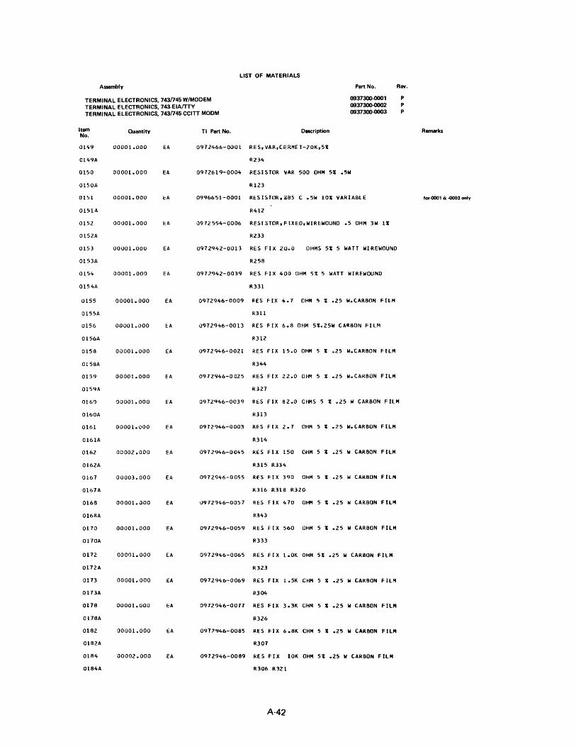
LIST OF MATERIALS
Assembly Part No. Rev.
TERMINAL ELECTRONICS. 743/745 W/MODEM 0937300·0001 P
TERMINAL ELECTRONICS. 743-EIA!TTY 0937300-0002 P
TERMINAL ELECTRONICS. 743/745 CCITT MODM 0937300-0003 P
Item Quantity No.
TI Part No. Description Remarks
0149 00001.000 EA 0912466-0001 RE S, VAR,CERME T-20K.5t
O149A R234
0150 00001.000 EA 0912619-0004 RESISTOR VAR 500 OHM 5~ .5W
0150A Rl23
0151 00001.000 EA 0996651-0001 RES ISTOR.@85 C .5W 10~ VARIABLE for-COO1 8. -0003 only
0151A R412
0152 00001.000 EA 0912554-0006 RESISTOR,FIXfD,WIREWOUND .5 OHM 3W U
0152A R233
0153 00001.000 EA 0912942-0013 RES FIX 20.0 OHMS 5t 5 WATT WIREWOUNO
0153A R258
0154 00001.000 EA 0912942-0039 RES F I X 400 OHM 5% 5 WATT WIREWOUNO
0154A R331
0155 00001.000 fA 0'H2946-0009 RES FIX 4.7 OHM 5 t .25 W.CAR80N FILM
0155A R311
0156 00001.000 I:A 0912946-0013 RES FIX 6.8 OHM 5%.25W CARBON FILM
0156A R312
0158 00001.000 EA 0912946-0021 RES FIX 15.0 OHM 5 ~ .25 W.CAR80N FILM
0158A R344
0159 00001.000 EA 0912946-0025 RES FIX 22.0 OHM 5 t .25 W.CARBON FILM
0159A R327
01(1) 00001.000 EA 0912946-0039 RES FIX 82.0 OHMS 5 ~ .25 W CAR80N FILM
0160A R313
0161 00001.000 EA 0912946-0003 RES FIX 2.1 OHM 5 t .25 W.CARBON FILM
0161A R314
0162 00002.000 EA 0912946-0045 RES FIX 150 OHM 5 t .25 W CARBON FILM
0162A R315 R334
0167 00003.000 EA 0'H2946-0055 RES FIX 390 OHM 5 ~ .25 W CARBON FILM
0lb1A R316 R318 R320
0168 00001.ilOO EA 0912946-0051 RES FIX 410 OHM 5 t .25 W CARBON FILM
0168A R343
0110 00001.000 EA 0912946-0059 RES fl X 560 OHM 5 t .25 W CARBON FILM
0170A R333
0112 COOnl.000 EA 0912946-0065 RES f I X 1.OK OHM 5~ .25 W CARBON FILM
0172A R323
0113 00001.000 EA 0972946-0069 RES fiX 1.5K OHM 5 t .25 W CARBON fILM
0173A R304
0118 00001.000 EA 0912946-0017 RES fIX 3.3K OHM 5 t .25 W CAR80N fILM
0118A R326
0182 00001.000 EA 0977946-0085 RES fIX 6.8K CHM 5 ~ .25 W CAR80N FILM
0182A R307
0184 00002.000 EA 0912946-0089 RES fIX 10K OHM 5' .25 W CARBON FILM
0184A R306 R321
A-42

LIST OF MATERIALS
Assembly Part No. Rev.
TERMINAL ELECTRONICS, 743/745 W/MODEM 0937300.tJOO1 P TERMINAL ELECTRONICS, 743-EIAmV 0937300.tJOO2 P TERMINAL ELECTRONICS, 743/745 CCITT MODM 0937300·0003 P
Item Quantity TI Part No. Description Remarks No.
0187 00002.000 I:: A 0972946-0095 HS fiX 18K OHM 5t .25 W CARBON FILM
0187A R324 R345
0192 00001.000 fA 0972946-0105 RES fiX 47 K OHM 5' t .25 W CA~BON FILM
0192A 11305
019<) 00001.000 EA 0972946-0129 RES F I X 470K OHM 5 t .25 W CAR80N FILM
C199A R328
0204 00002.000 EA 0972946-0037 RES FIX 68.0 OHM 5 , .25 W.CARBON FILM for-0003 only
0204A R317 R346
0207 00001.000 fA 0972947-0029 RES FIX 33 OHM 5 t .5 W CARBON FILM
0207A R322
0208 00002.000 EA 0972947-0057 RES FIX 470 CHM 5t .5 W CARBON FILM
020BA R301 R303
0211 00001.000 EA 0972947-0117 RES FIX 150K CHM 5l.5W CARBON FILM
0211A R329
0212 00001.000 EA 0972 cHS-0069 RES fiX COMP 47 OHMS 1.0W 5t
0212A R302
0213 00001.000 EA 0972978-0093 RES fIX COMP 470 OHMS 1.0W 5t
0213A RIl9
0214 00001.000 (A 0972978-0100 RES FIX COMP 910 OHMS 1.OW 5t
0214A R368
0215 00001.000 EA 0972978-0113 RES f-IXED 3.3K OHMS 1.0 WATT 51
021~A RIl8
- 0221 00002.000 EA 0972946-0037 RES fIX 68.0 OHM 5 t .25 W.CARBON FILM for-0002 only
_ 0221A R317 R346
0226 00001.000 EA 0972498-0001 CClNN,OBL ROW,EOGE MTG-20 POSITIONS
0226A JIOl
0227 00001.000 EA 0996260-0001 RECEPTAClE,3-PIN At PWR
0227A J301
0230 00001.000 EA 0416434-0203 FUSE 2.0 A 250V 3AG
0230A f301
On1 00003.000 EA 0~30588-0008 FUSE ,CARTRI OGE 2 AMP
0231A F201 F251 F252
0234 00001. 000 EA 0972602-0001 XFORMER,SW RGLTR,PWR SPLV 596UH+I-60UH
0234A 1301
0235 00001.000 EA 0972614-0001 TRANSFORMER. TOIlOIO
0235A T302
0237 00001.000 EA 0972445-0001 CRYSTAl,12 MHZ ,QUARTZ
0237A YOOI
0239 00001.000 EA 097246-1-0001 01 SC. SOUND-PI EZO-ELECT 3200 + 600HZ
0239A [}SOOI
0241 00001.000 EA 0996592-0001 SWITCH.TOGGLE,OPOl 3A/250 VAt 6A/120 VAt
0241A 5301
A-43
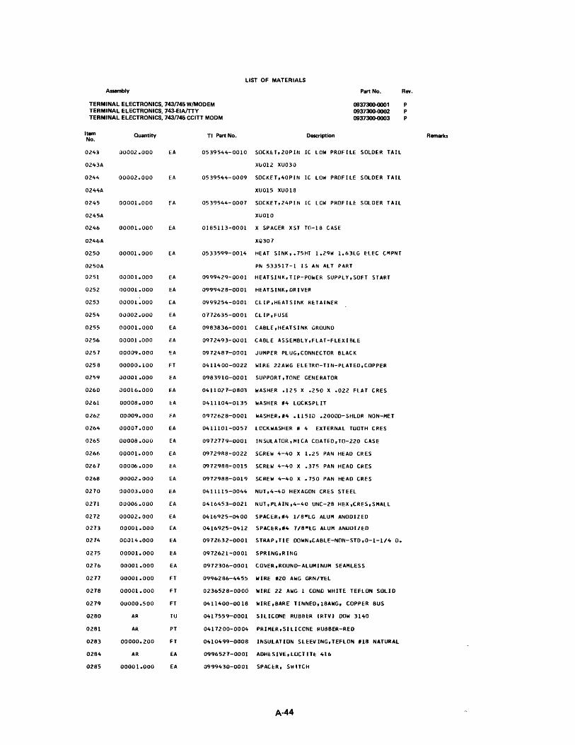
LIST OF MATERIALS
Assembly Part No.
TERMINAL ELECTRONICS, 743n45 W/MODEM TERMINAL ELECTRONICS, 743-EIAmV TERMINAL ELECTRONICS, 743n45 CCITT MODM
0937300-0001 0937300-0002 0937300-0003
Item No.
0243
0243A
0244
0244A
0245
0245A
0246
0246A
0250
0250A
0251
0252
0253
0254
0255
0256
0257
0258
0259
0260
0261
0262
0264
0265
0266
0267
0268
0270
0271
0272
0273
0274
0275
0276
0277
0278
0279
0280
0281
0283
0284
0285
Quantity
(lO002.000
00002.000
00001.000
00001.000
00001.000
00001.000
00001.000
00001.000
00002.000
00001.000
00001.000
00009.000
00000.100
00001.000
00016.000
OOOOS.OOO
00009.000
00007.000
00008.000
00001.000
00006 .000
00002.000
00003.000
00006.000
00002.000
00001.000
00014.000
00001.000
00001.000
00001.000
00001.000
00000.500
AR
AR
00000.200
AR
00001.000
EA
EA
fA
EA
EA
EA
EA
EA
EA
fA
EA
EA
FT
EA
EA
EA
EA
EA
EA
EA
EA
EA
EA
EA
EA
EA
EA
EA
EA
fT
fT
FT
TU
PT
FT
EA
EA
TI Part No. Description
0539544-0010 SOCKET,20PIN IC lOW PROFilE SOLDER TAIL
XlJ012 XUOJO
0539544-0009 SOCKET,40PIN IC lOW PROFILE SOLDER TAIL
XU015 XU018
0539544-0007 SOCKET,24PIN IC LOW PROFILE SOLDER TAll
XUOIO
018511J-0001 X SPACER XST TO-18 CASE
XQJ07
0533599-0014 HEAT SINK,.75HT 1.29W 1.63LG flEC C~PNT
PN 533517-1 IS AN AlT PART
0999429-0001 HEATSJNK,TIP-POwER SUPPLY,SOFT START
0999428-0001 HEATSINK,DRIVER
0999254-0001 ClIP.HfATSINK RETAINER
0772635-0001 CLIP,FUSE
0983836-0001 CA8lE,HEATSINK GROUNO
0972493-0001 CABLE ASSEMBLY,FLAT-FlEXISLE
0972487-0001 JUMPER PlUG,CONNECTOR BLACK
0411400-0022 WIRE 22AWG ElETRO-TIN-PlATEO,COPPER
0983910-0001 SUPPORT,TONE GENERATOR
0411027-0B03 WASHER .125 X .250 X .022 FLAT CRES
0411104-0135 WASHER.4 LOCKSPLIT
0972628-0001 wASHER,.4 .11510 .20000-SHLOR NON-MET
0411101-0057 LOCKWASHER * 4 EXTERNAL TUOTH CRES
0972779-0001 INSUlATOR,HICA COATEO,TO-220 CASE
097298B-0022 SCREW 4-40 X 1.25 PAN HEAO CRES
0972988-0015 SCREW 4-40 X .375 PAN HEAO CRES
0972988-0019 SCREW 4-40 X .750 PAN HEAD CRES
0411115-0044 NUT,4-40 HEXAGON CRES STEEL
0416453-0021 NUT,PLAIN,4-40 UNC-2B HEX,CRES,SMALL
0416925-0400 SPACER,'4 1/8"LG ALUM ANODIZED
0416925-0412 SPACER,'4 7/8"LG ALUM ANUDIZED
0972632-0001 STRAP,rlE DOWN,CABlE-NON-STD,0-1-1/4 D.
0972621-0001 SPRING,RING
0972306-0001 CO~ER,ROUND-ALUMINUM SEAMLESS
0996286-4455 WIRE .20 AWG GRN/YEl
0236528-0000 WIRE 22 AWG 1 CDND WHITE TEfLON SOLID
0411400-0018 WIRE~8ARE TINNEO,18AWG. COPPER 8US
0417559-0001 SILICONE RUBBER (RrV) DOW 3140
0417200-0004 PRIMER,SILICONE RUSBER-RED
0410499-0008 INSULATION SLEEVING,TEFLON '18 NATURAL
0996521-0001 ADHESIVE,LOCTITt 416
Q999430-0001 SPACER, SWlTCH
A-44
Rev.
P P P
Remarks
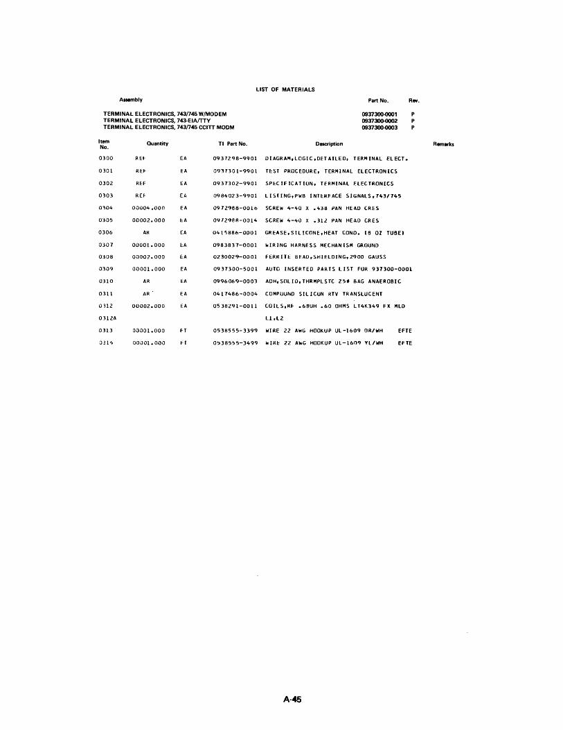
LIST OF MATERIALS
Assembly Part No. Rev.
TERMINAL ELECTRONICS, 743/745 W/MODEM TERMINAL ELECTRONICS, 743·EIAITTY TERMINAL ELECTRONICS, 743/745 CCITT MODM
0937300"()()()1 0937300..()()()2 0937300"()()()3
p p P
Item auantity No.
TI Part No. Description
0300 RH- EA 0937298-9901 DIAGRAM.lOGIC,DETAllEO, TERMINAL ELECT.
0301 REf EA 0931301-9901 TE:ST PROCEDURE, TERMINAL ELECTRONICS
0302 RE:f EA 0937302-9901 SPl:ClfICATION, TERMINAL ELECTRONICS
0303 REf- EA 0984023-9901 LISTING,PWB INTERFACE SIGNALS,1431145
0304 00004.000 EA 0912988-0016 SCREW 4-40 X .438 PAN HEAD CRES
0305 00002.000 loA 097298A-0014 SCREW 4-40 X .312 PAN HEAD CRES
0306 AR EA 041~886-0001 GREASE,SILICONE,HEAT CONDo (8 01 TUBEI
0307 00001.000 f::A 0983831-0001 wiRING HARNESS MECHANISM GROUND
0308 00002.000 EA 0230029-0001 fERRITE 8EAD,SHIElDING,2900 GAUSS
0309 00001.000 EA 0931300-5001 AUTO INSERTED PARTS LIST FOR 931300-0001
0310 AR EA 0996069-0003 ADH,SOLID,THRMPlSTC 25. BAG ANAEROBIC
0311 AR EA 0411486-0004 COMPUUND SILICUN RTV TRANSLUCENT
0312 00002.000 EA 0538291-0011 COILS,Rf .68UH .60 OHMS LT4K349 FX "LD
0312A ll,L2
0313 00001.000 H 0538555-3399 WIRE 22 AWG HOOKUP UL-1609 OR/WH EFTE
0314 00001. 000 fT 0538555-3499 wiRE 22 AwG HOOKUP Ul-1609 Yl/WH EfTE
A-45
Remarks

o
-
c
a
A
e I 7 J
'I
6 I !5
I!!l nlEs. TRANSl~T~RS ARt M0UNTcl) If)N HfAT!INr(S.
I§) IF NECfSSARY II SE(;C'fD IUSIST"R. IS INSTALLED AT U';lT TEST IN L¢CATI¢N '(>4id! IIJi/ HM AS RCQUlIHIJ m ~RD(R. T~ ACHUVE MAr >(/SPACE SYMME7RY.
§] RESrSTo1JRS WIn~ N¢ VI.LUcS ~PECl~lcl) ARE NOT IN!TALLE4J ,,/oJ 115V FCl>.
~ lila IS USED ~OR I)PTlONAL AtM AND IS INSTALLED FR0M C(}NFIGLUI.ATICJN GUILE AT U'JlT AS:EM8LY.
!ill ",or lNST!> LED, r(ll1 rUTU/?( US! "NLY
[ill Rr;V·A' B~"RPS WILL NOT HIIVE C3" "R JUM?fR WIRe. THESe PtlNTS WIlL f:! CrtJ/./IJeCT(D B'" (TtH RuN T¢ -+160V/{.
[!§] FERRITE BE.AD INSTALLED ON STAKE. PIN FOR REV B i c pce'S ONLY
~ £. ret! RfPLACED WI7t! COIL (<;BMJ.) OR FERRITE. 8[AD':> (2) 011 RU E. f LATER PC8'S
~ ALL REV Ai [ARdER PC/<,'S WILL HAilE R373 INSTALLED. REV B PCBS WILL HAVl liTHER R373 OR .IU!.IPE.R W,IIE REV C WILL HAVE. .J&!.IP£R "'RE. RllI. E f LATER WILL HAVE ETCH.
>5V ----+~J[~c-,--------------~1~-c-6-,c-8-,-cl-,,-c-,4-,-cl-8,-C-I~-'(-2-~-(-21--'~
T :Jv T • • • • .O~7;;g~ • • T L. ______________ • __ ~ __________________ ~~------~
+IZV ____ ~--__ -_--.-__ ~-----
I Cf. 1 C4 I CI7 ~b' (408,C4-15, r4Z" 14<9
~~i _~_gV ______ ~~3_fii I~gi ___ ~!l_· ___ · __ .~_4_7_·~_~_g_~_:· ___ ·_~'F~ ____ ---.
-5V~13 l,Co47 T +BO% I -~OYo
I 1 CIS
T·047 ,.-BOY, -£01'0
-'2V~---------------~--I~~--------------'
1(5 e40 I, (1.,4 (425, (430 ...J..._'_ .047 • • • • • • •
-'i~~ I .047:~g~
1
! 4 I 3 J N0TE5: UNLESS (/)THERWISIf. SPECIFIED;
t. ALL DEVICE TYPES ARC PREFIXED WlTH SN74.
2. vee IS APPLlCl> T~ PIN 14 ~F IiL( 14-·PIN IC'$ AN~ PIN '" ~F ioU 'i.. PIN Ie '$ ,
a. GIt4>UND IS APPLIED T~ pr'~ 7 q,~ IiLL 14·PIN IC's AND PIN" (/)1' ALL "'·PIN IC'S.
4. DeVICE T'fPl, PIN NUM~ERS, A"l> REFERCNCC DeSlGNIlT'I/f, ~F Ie 15 SHg,W/J AS F"LL0WS;
~~ ~
00 "'Nil 04 .. DEVICE TYPE 4,S,AND"" PIN AlUM.HR.S
U21
lJI4 AND U21 • REI'EI!EAlC~ DCSIGNATItJR
5. RfSISTt1>RS ARE 1/4 WIlTT, !!"7 ••
,. DlfJ>DES NItJT MARKED ARE IN9'48.
7. AMPLIFIER.S N~T MARKED ARc RC4~~8P.
9. (/)N RC45511P AMPI.IFIeRS, PIN 4 IS TI£D .,." -12V f1ND PIN 8 13 TIED TItJ -+-'2V.
9. 0 % SVM6(/)L U5;O ""'R 'f" NUMBERS WHICH HAYE A :;QUAR E PIN.
10. SHtfTS 8 AND 9 SHItJW THE Mt>D~M/AeI/)USTlC Ct1lUPLER ClRCUITRY; SHEET II 'lPPLIES T(/) 937298 - 0001 ASSY, I.ND SHeET 9 APPLIES r(J 937298-n003 ASSY.
1/. /oJ(/) TEST PIbINTS MAY I!E MrtlVEl> WITl-IftUT PIU~R 4PPI?,OVAI. By TCST '::NGINE:CRINu.
q~8
~ U4
f~_9_J'~~8b ~
UZ7
~ ~~
U"
SPARES
2 I
o
c

D
c
B
A
8
,----------1 'SV R~!5 INSTALLED I
I 33K I'>liR I I -0001 ~'W I I AND I I 33( -ODO,AlSY I
7
"'ICR</JI'I/</JNC , .'402
~PtAK.1 k'. J4)1
L - - - - -~-_-_-_-_-_J __ R_L_2 __ ,<11 SH 5
J403
I RLI
I I I RL2
I I I I I I I
8 7
6 5 4
I J402
6 5 4
.... 3011
I L
+30V
C I RCUITR'i
E 310
3
P0WER SUPPLY
+/2. V +5V -sv -12 V
TEST ACC~5S (3" <324 £328 020 P¢6~ PADS
+12V +5 V -5V
L¢AD
- 12V
XMITDATA
lOt ~437 +5V 3.3K
~/W] DSI(/RL2
'** R435 +5V 3.31<
DV!.2
I I> " I 7
I I> 4-
DT/XI I ~--+--+------------------~s
I
937298 SHUT 2
D
c
B
A
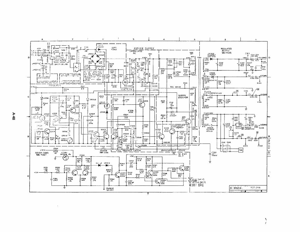
1 f

8 7 6 5 4 3
SYUC
o
+I.r .f FR¢M{~'2~_r--.~~-----------+~--~.~2~~-;------------_--+------________ ~.Z~ __ ~ SM !5 ~:_Y'.- ~e_MI-
~~,~~--+-r---.:;i7;::;;:~S""CI"'-I/-------------t-~--"""~::.;~:;~!"'CI~~-++----------------------_+--------------------:;.:·;c.:;.~f-'5':.::~:..-,
I I
+5V 14~''(''l-W-]' DO +5V 14ru('""'i:~IO
I I, III I 15 I I, »2 I I"
1\5 111>".,1-
',I h I I" D~ I I. L~~ L~-.J
I '-", II}
L~~ 117
" I l1<TCr= I IIUN ., i
C
:70
F~QM
» SH.~;;}
ct Ell RESCT
CPU Hf>Lb
HS
RI" 5/0
FR\!>'" ReAIlV'
a SH 5
1''' now 1J7 ::0 THRU D7
I?CVlIATA
TPtJ,M {' 5~. 5
_. ___ P_k..'-t._M_-_
HVLIlTA
A
8 7 6 5 4
AO
£31 Ell A 14
E2S AO
flS TEST Er" ,-~l ~'ACCESS ti1
AS t17 E42
A~ n, [41
£39 A7
OJ
All
A/O
Aq
A8
T ... RU
~TllS>l.5
~,'f.' ~T¢.5"5
.4. rc;.----
-5" -----:.. "B" +5V-+ ,Ie +/2"----2. v6~
'--¥.-~~:~ TM5 ::0'8 ,,--==-_'-=->" A Z TM 5 5504
A3 1' /43
AIS .e SYNC
" S~>lC +1 20 ~ I 42 21 +2
5£N5"1I Z2S£IJ INT 23 INT
cwo 39 INO INI 38 r>JI INZ 37 INt H') 3" IN) IN4 35 IN'" INS H INS IN. 3) INi. IN7 32 I",'
~l>O ~-4,- ~~
;,1 10 D3 1>4 • 1>4 D5 8 OS ll" , D. 01 • D7
RC~Rl UI8
</oUT 0 p.Z::..;.4 __ ¢_R_0-_
ClUT I 1>2:..:;5_-..:.</o_R_' -_
¢UT Z p=2"'---..:.I1>_R_2-_
¢UT4 t:>-2,,::S_-=<t...:..R4_-_
¢UT5 t.>"-'Z9_..:.CI...:..R 5=--_
/l>Un. r>"-30 __ e_~,,_-_
31 'J,R7-</oUT7--
TI/¢ 40 XltTMTA T¢ SH. 5
(1-"_55 ____ --' Wi?-
..-______ ....:D:....O ___ } TqJ S~ 5
DO j £30
I'~-~~~~-.~ g: D3 EZ~ b4 fZI D5 E22
"---~g'-';'----~ ~ ~ ~
o
c
B
A
» 0, o
o
-
c
B
-
A
~ ___ 8 ______ ~1 _____ 7 ___________ ~1~~ __ 6 ______ ~1 _____ 5 ____ ~!~ ____ 4~ ____ ~' ____ ~3~ ____ ~1 ____ ~2~ ____ ~1 ____ ~1~ __ ~
'I :;:-;~~=~I ~ :;'~,f ,.. 1,''----------:-,:---- ~:--~;~t2V-I, 'I ~~u:45 IJ r;~P"~ .O~/j 1:1 ~fV oF " ;;_~1: __ ~_, f:..e~ STtPPtRB ~4 ~:4 ::~:: I
~'~TI C7 ,tV ~~ I , r-~ ~ I' fA'0M ~0NLlNC-..- Uc5-IO 2K ,
i ~~':I C7 '; ~t:l, ,IH I? ;LK .,- ~2'f;5N153SD 7lRZ ~ c~:pf' .':'i ~I ,5H "+sv ~; ~I :1 -7'5
OTR I , ~ IODp~ IJ. ~~ ~.~ g", glg'.!! ~'I {'f.MTOIlTA I E> ~13 XMTD I
.70 ~4 i-1t" 175 J~ CK, .2]~ ;- (UI6-40)3LS~.ffi5.E __ -Y!.J __
"
---'V ~t I I T3 ~2P, 15 ~i- ,3 L' 'I i I/C~'~~"ZI , -r- ~; C9 I I e RLYnATA /I 'LS'" 12 6
1 _.Y1 I.. ~ 12 RCVO I CLq,CK &. CUI +z.- 66pt" (u/S.5) ~: L +5 .
'L DIVIDER CLKtO ~+5V -= ,II, If-I (~~~~)-I Ria U7 :: '"'N I, J /'1 CDET I _ ~ 2Z0 NC.4-J I r~ -;:;f-;;;-f---------_, I .-- ------ ---------------- hi ,,1 ~'~ I ~, ~, ~: 07UMPERSINSTIILLWI ,
I I "': "': '" I 01'1 PORTABLE I
~ WAIT INTERRUPT Ri~8@ LUI...J p~391 ... Ii Ill'? -sj UNIT 0NLY I I I /I FRtlM S>I.4 ACKN;;,'JLEDGE I I . J)SR. - - ~i I ~ I ~ I 0 (SH SI-i. 8' 'IN!) 9) l
&. READY Rl z 6 L \u '" ~ I ~ ~~\II rnAicR 12 ,...~ II TERMINAL INTERFACE J40H/ (51-1 c) ---------------' I I I ~, 13 ~~5Ib9G: WiA L04 5 L...:: _____________________ --.J
, Ub ~4 "JU3 G ~ INTA u4 E> WAlT- ,PW1{CLI( PW/?CLI( EZ I + 5":15 1[1
'PWRCLK.
LE58 T¢ C 203 SH. 7
"
00 IF<Jf-==-;,7 DORE. IK t5V ZH':: I +5'1 ,'~ A vet Q.fI ~ +5"- 5 J +5'1 ~IO ~t~;i~5V: ~-5V :~G"~d:~ }
LS.I ua ! CLK+Z I 93A 9 14 ,'C IZ CIO' + CIOI £9 I I Co .. ,) I 8 Q'r- r~1- f':;~ L ltF , ~~ 12 RI9 • ';'8 92A· 22UF", I 6' U JIOI
SYNC- '0: I" SYNC' S10 ~iO' 9QCUB "!""!+-12c;.!~ r A9 ~'Of-----r---..~ 7 XZ>3
I I 1(,04 I 5 010 1 I ~ RD. uZ QlI /I (., '1 '-1 J~ L.o-~ I~ EIQ 0 LU_A.J U27 , • f tOI ae ~ (UA's"OlS ) II ---r---_ ~ 121 I
I .... REiley" I (;"11 7 W8 8 ~ l~ to XlIZ • (Ul5-23, 1 ~ £02 CJ, -=--- L..:OEIZ3 I) 20
L ____ _______ ~~~_~B __ ~ ___ '_~ -= ~~j ::,~ij~ 12 ~ 5 Xlii ~E"ol I" 10
" ---- ------------------f------------l ~ (UI:'~') 13 ~ ~ ::: t::o!I08 ,)8
1£16 <;> I AI 14'~ 3 19 I (U'N" ~C/tt I I PHD- r+---+-+-lH---______ -+-_~P,~RO~M:.:.::.- I 110 15 ~ 2. 'fDI 9
I E(O~-_~~++_--++_I_+-_. (U6-I,SH.4) I (I.M-IS. 98"'4 UIO/ ~EI09 I 1£
290
I . pc? +5'1 R~3000- C_y4 C'fR[7 J 5 U7 I +l5~V~ -5'1~ GND PRINT I. 12 (5'"1.4) J --~-~hSJ2\ 6 cnlSTRBE- CIO' cloe HEAD ~I
I 510 RIIM- 7:TPI'l ~ (UZ~-9 SH ") I FR<J,M < .047 I + .041 DRIVC/{5 _I~II 10 1>.!.!.11_++-:~-=---, J, ~O L53?\.U78 CTL2S~RB~- SH.4- £ltOuS, "_+ I 8 i.lftF I , ~LS041 0'" R;:. .. :l- 154 131ZIII0197 (UZ5-9SH") I ' ~
US un s 13 1£5 ~R~ ~ - t:::Jx; 7 X .... 4 ~ E 107 I I Ell ~az-'" l' ~z 1314 1'5 y", Y1 us I 118 ., ~
~ '.1 LS/38 Uti 12 I (U/':>-/8,SH.4) 10 17 7 ,
~ 6 EIS (UI5·~') Lr--..~ L )(1).5..-n EI20 I
~ -F~ G.lA ABC 5 I At /I II I~" I - 17
I <I LSII " Rel1l- Ttj\ 1112 1 2 ~ 2Jt:'09, (U,s·'" ~_ :5 '(1)7 ~el"5 I
I UII)-CO L-2 - Q~NC I "" 12 r-, r 5
I
I us EM SH...." II ,;;: ~ :c;:,l. 7 L,CRt
PHDSTRBE (UI~';Z) 13 r:r--:c 4- Yb~ r £117 1 14
~'" L .~ T J I (U/~':> 14 t:fJ:> 3 YZ>S ro C/O. I, 4
, I'Re/lllStl.4 I (U'~·t 15 L...r--r:: it '1'1>4 roe"" LJ3 f~ (uIN') 98b/4 UI02. L ___ -~------_~DDRESS ~EC~D~~~~.:. ___ =_·~ ______ J 1'HDSiRB£
f
o
I--
c
B -
A
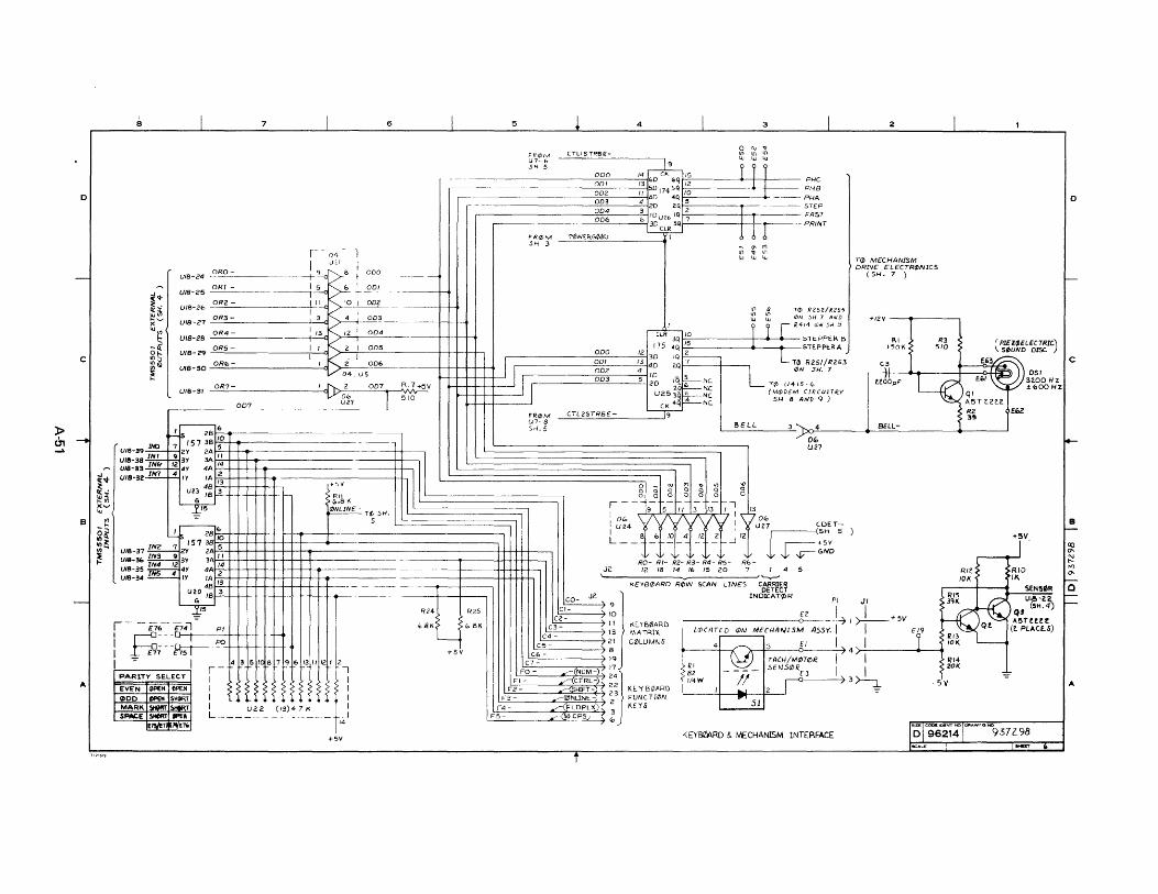
I
8
0
C
» 0, - U18-39
UltI-38 UI8-33
~-t U18-3Z
It: • luX ... (/)
><'-'
'" B -~ ~~ ~~ ut8-37
~ U/8-.36
U18-35 U/8-34
A
~~ ~! )(
'<J", ~
-~ Of.. 10;:) IOQ
~
~ IiW 1&t
7 6
LJ,-' ORO-
UIB-24 --
ORI -UIB-25
U18-2b OR2 -
UIB-27 OR3-
OR4-U/8-2B
UIS-i!9 OR5 -
UIS-30 ORb-
UIB-31 OR7--=--'-'---------.....:/--<c{» 2 OD7
_______ 3~7 ____ 1 007 -
'----6 -------~S ,,8
IS? 38 10
,2 2Y "A~-+--I--<'-~~~----------------
~3Y 3A" ~ 4Y 4A 14
,..! IY IA 2 4B 13
U23 /B 3 Ii
15
,-- - r- RII 10.8 K
~T"'SH.
5
FR(/JM CTLISTFlB.-U7- ~
5~ 5 000
001
OD2 003
[-004
OD6
FR(f;M Pa\WER.G~D $;-1 .3
000
001
OD2 003
~v 510
FRlbM CTL2STRB E-U7- 8 SH.5
4
~ '" In lu I.u
Ui '" 't lu lu
~ I.u
CLR 3Q 10
175 4q 15
123D IQ 2 13
40 C'.Q 7 4
/0
~~ ~ "D Nt:. NC
U253Q \I NC CK 4q 14 NC.
9
BELL
,I 13
3
~ I.u
PHC PHB
---PHA
--- PRlNT
'" In I.u
~ 71/) R252/RC55
lu (/IN 51! 7 ~"'D
R414 (/IN ~Ii 5
!:>TEPPEF\ B STEPPERA
LT0 R2511n5:!. 0N SH. 7
T0 U4-15-i;, (M</JDEM CIRCUlTR.Y'
SH 8 AND 9 )
2
T0 MECHANISM ORNE ELECTR0NIC5
(5H. 7 )
+12 V
1\1 R3 l'=iOK 510
-=-"---6 5 L~~============~
.---"7<-""><-~..___'_':,...__.Jc.:;.....L:., I OlD
I UZ7 CDET-~~ "B to
~2:57 ~~ 5
~3Y 3A:! ~~: ~: 2
4B 13
U~ IB 3 ~+-+--j--++-+-~--+----I-W--- - - ---- -- -____<p>-----t---,
15
-=-R24
.,8K
1'5V
R2S
",81(
',2 ~5H 5 .J r-- +5V
-.J.., W-- GNO
RD-- RI-- R2- R3- R4- R5-- R6--J 12 18 14 16 15 20 7 I 4 5
\ -------...---------.-KEYB'1>P.RO R~W SCAN LINES
C~9
CARRIER DETECT
INDICAT0R PI JI
C~=- / ;~ "UB0ARD [2 I I +
,-----------0--- - -~ 1)-7---- 5V MECHANISM 45S'(. I I EI9
Rle 10K
CO- Je. l C-'-'4;-=-------') 13 MA TRI'l.
C'=5-__ ----~21 C0LUMfJS CL:6'-=_-----4 B
L<lJCATtD </>N
4 3 ~~4~1------~~-4 TACH/MqJT0R. I I C~7c:; __ -----~ 19
FO
FI-- ~CTRL--) 24
:.>:-,2~--___ ~~0:=-=:IHI::....FT=--~) 2; KE.YBVl,ARD '--F--'3'----___ .... ....---~<al"'N.:::U:::.N:..::E'-'-/~ ~ FUNC TI0N
£1 82 1/4W II
5ENS0Rf3
I I -=------7 3 ~
L-__ ~~~~ __ ~2,---~ 7
51
J?14 20K
--5V ....---(NUM--) 17}
>4 - .. -----(FLDPLl() K[YS ~F~5~--________ ~v~-~C~~C~P~S~~ ~
+SV KEY~RD & Iv'ECHANISM INTERFACE
DSI 3~OO Hz .:!:bOO HZ
.. 5V
RIO IK
SEN5~R
ul!>-a~ (SH.4
Q.f A5T~~2t
(z. PLACE.S)
o
c
B
q)
'" '" to-
'" ()'o
0
A
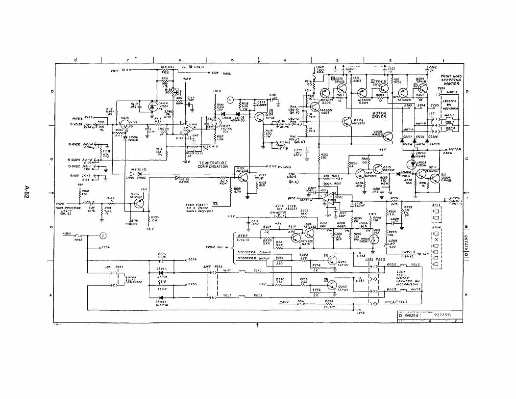
c
B
A
7 6 4 3 2
:tez.OI .01
RrsrLECT VRF..F EIII O-----...--"RVI,2Al~~'__ ____ _OO EIZ4 R5EL
RIll +IZV
+lOV
MOTOR pvms EllS DRIVER
o VOLTS .T'Ol-"~IV'v-""""""",~-, rtr;---_~'VV'...-..--t---=~, EI14
~20!5 RI07 1.81'.
A TZZ PHC---*--+---------t----~~~
O-GNOE RI15 383 .Io/a
R SL4\PE JI()I'Z f-<I>+---t----i----------' £IOZ
P-GNDC Jf,b-,' ~ IN4152 (2)
-12 V TEMPERATURE COMPENSATION
:TIOI-I~U~~. h) PGND
EI18 C ZI+
.001 I 200V =
r-:::~-Ir---.() ElIl PVSWB
R2ll 2ZO
GNOS JIO/-3 ~
FI03 o-.:...J * +5~
~*-~------------------~ F~------~-~~~-~~ uz,-z eRIOI eRIOl
P~T---~~~~~~~~-1-""""'+{ rROI~ PF/oqsscM
1N914B eRI03 ... 71\
RI04
r~4lM CJ5H-) -,p....;;G'--_J SH 3 (Pew'~ SUI'/>lY SC(Tr~l()
RIDS @H.h) 8to
(d~.h;l -5V +It v
RIOS 2K
+/2V --....-----~.;v...."....--__'\,IV'v---_,
CZII R209
-Ilo V
C213 2t;"fF
~ ______________________ ~ __ ~r __ -4~ __ ~Et5'
ZK R20f> 12.1 K
,.,.. 1'1'. R207 953 1"I°cm~ , {~~~::":'_1~w~~~·~~~0~)~~~~==~_-* ___ ~ ____ ~ __ ",,,, ___ ~
STEPPER B (ut.-/o)
J251 P2S1
: In: HfAl!
I LIFT
r----172 ,:,t>UtJt>lli
CR e! ': J25t P252 WHT I
r---~---+------------~I· s~1 ~~~~ 1N4134
C212 -±jt--........ ---o E 2 55
25MF
I I I I
L--~ ____ +-____ ~b~,I __ Y~E~L~/~
BLKI
1!252 U55
+5V 330 200
RED/
ft1
RZZS
RZU 10K
lez03 ,..,....47 + sov I
lceoz .01
PRINT IIEII1) STEPPIIIG M~T~R.
M¢TiJA
EZOI J201-1
Jis! MOT·R R233 '-I
.5Jl liD I IY. 3W :zo I
L_...J JZ!>l. r-I liD 1 1 X 1 1 I 130 I I I
PWIULI( T¢ 5115 40 I (U~8-8) I!>o I
1 I 1"01 L_...J
CR~51 IN4934
+30V F251 1'zse ~ ____ -o~9 ________ ~~ ______ ~ ____ -?4>-__ w_w_r_2~/_Y_c_'_Z ____ ~ 20,51'1
'------------------------------------------------------------------------------------------------------~-o [25<: 9372.98
c
0
C
B
~ 0-
'" "-N) 0-
Q
A

0
e
B
A
4
R4fl
R444
L41t 'li.
r - cm7t-----l £40&
I TP MI(F( TR. £4'0 I I Z 1140 INT6lTI! TP
I U40' ,. J I- ~FmiNcEINi:£6W0;r-c~ .~.~ I I CR4" "." 1(11( ,lt4SI
el1413 1147., '01( , .. ~
2
us AC~U5TIC C(JiuPLE~ / M<f>DEM (0UGINATE M01>t)
{F'MK 2U5 C409 RECEIVER F'SP 2015 'NT/(
("MK TRANSMITTER
lFJP
JH3
.'2V
.. -:J IA/SrAUIl>
I ~!·I>I :~:,. -:!~~ L _.J
1270
1070
L... ____ --==-=:..=-:===-=-=---_______ ---. ___________ _ ____________ ~~. ____ ~~~E~\~~ __________ __
[)
c
B

c
B
A
e 7 6 4 3 2
CCITT AC~USTIC C(/)UPLE.R/M~DEM (0~lGJNATe Mt1JJ)~)
rTf/I; SHE iT APPLIES T'jII' I 4SSY 937300 -OD():S I L __________ ..J
r I'M/( "50 RECEIVER lFSP 1850
{
FMI< '180 TRANSMITTER. FSP 1/80 r---®
==~~-------------------------------~
I CU~I CR41, I .~ )/'.. '
I ~f <-.:~ Ck4~''7-----r-------------------------l--------'''' I / ~ ~ IN'14~1l I ~ " ',' "'L JU· ... F£R I C~?Z~ 'lcR4/8 1£4:':,; /' _ ~t ~D( ~;~ :
L = I r4C'1l Co.f :£i. ~d,2t5 - L __________ J
------';4~3'3
X'-I1I T ':;k Ttl
CARRIEf -I'LV
~ R423 A42'2 8<'<OK ,5j1,
~----- .~~~~-
~ 452 J40) ~~ ____ ~~/,~5~Kr-____ -+~ ______ ~E~I_A_R __ CV_~_A_T_A ____ 78
.'2V
o
c
B
A

"
e 7 15 !5
D
c
9J.J" 14'1e ,.,., A= 5 •• e.OK ~c~I.Ol(d
>!...4 __ r-_---.5-~--l Q&.1
3 2
CCITT (J"P~N,NTT) AC~USTlC c~uPLu/M~D£M ( ~/U(JINAT~ Me1J£)
r;. -:/; ;;;i"r -;';;'i;6S T.' II/$Sr937300-0,Q4 I L __________ .J
•• 67 2.7
."/2 ~ R4'2 'O/( 7S~
T'II111."IT I -." ,-eVE. '40'9 ""JUST lJO
RECEIVE~ !'IIII( '610 . l'.sp /1$0 .
T~ANSMITT!R. {~"'K ''0 ~£P "'0
~---=~~~~--~-~~~~-~~~--------------------~--.----LI-_~=_~~------------~~--~_-_-_-_~_~--~~~
D
c
•
o
A

o
-
c
B
-
A
8 \ 7
NOTIS L'''-ESS OTHERW'SE SF-Cf'ED l c... -.:- "':; CCMf'Ol'.E',T l.£»O)5 ~lONAL. 2 r.c. "':IT =..0£:1'1. eN c.DMf'ONE,~i SlOE.
\
~ "'IS'" -OOLINe. .a.E~ ON ~TH SIDES OF eao.RO TO PREVENT s:._~E'" "ROM E'llTt",NG HOLE~
l!l ~'Q A~~ ':i~~'oAP-IN sAFETY CCM:R (ITI:I'12'4);
s. Ei!Z!2 ":"-"TES :.JMPONENT~ NOT u-,EO. CO ...... , ~"'D LE";'TH FROM CONDUC.TOR S.DE or 80ARD I!> .075
6
t::' ~ "':"ili~~~~-;f~~~H ON P'w'eo OrrM 1);l5tWltE -;-",..,.e, WITt' ITEN L"!1'3 ~ ~~~ WITH TIJI. "'~A7e:C .:c'lTACT £:>10 Ci'" CAOL.E IN eOMD. ~ ~"!(ITEI1 2-4+) TO E:.~ CAA!:>SIS c,'IID.
[§ ~';2_~~~~, ~~C~ ~~~;3T;(·,",I.~I",3<.o5,~!a2,5" [[Jr:.~t~~';~~ ~5.;~T~5!r~D~T \..NIT CONFIGUfU.TIOlo;
~ ~J"~~lJ;'P~1~·~W.o;~~~RZ3~1&~~~~I~t~~~~, g: ~.:~:.."tt~p~7x.' ~£M 240U'N P'NSf}TEM ~~fl AT (£~ t £.5(5)
~g~ ~~2..~ ~:i4g;E~(/.-y,.~~V~=:'7)~~~:)5 -H~,l( .'t£.:'~~~4 AI. ON -D004 ONLV]
[[ oF ~E':; -'~'WI<AP ~,.,- 5.Jr....I: BE I'rlSITICJHE::J eN (~MDUCTCJI? !>IDf OF FWB ~ :)O.J)ER ""IRE: TO K>l.E. IN GROUND P' .. ANE ON ,.,,,,,13 (E~57)
Iii ';t~~~~r::;."1 c.6B eE.TW£EN(£~O, E3b1) '-NO(E3"?> I E:.?>~. IiZI IN5T"_ .. fU5E CUF" TH [HO "T"""~ TO OUTSiDE or F"U$£ R:l!>ITION. lit T3:l - ~ I i 110- ii' it I ~C;i i =- if Ii HF-~ F,,-~ J5TM£:NT ~.,.Q.JLD F:A.C.E EDG.E c: F't. !3OA..~D ~ =>£c.:JR£ TO P"'w'B '\NITH
~ +'1f!1t';3~f.i'4f a..l)t3?H'D.~.5W~"T8",,~":~ ~'~EEN:::'~"r'~ ... ~'frl-&I't£W~ 'O.3N-l.B5-
~ c;;;ex TE~1/T~tTI:gE,,{;;;';~~o~O AT APPROlCIM"TLY +siTOw'ARD CR~\ ~ ~~~",,~~~~~Z.1-.?2 ~ErU~T''fi~L'F(':«~ THAT T'£ ~TAL. CASE ~ .!.I'1"'ERS INSTAlLED A-r L.'NIT CONF"IC,:"lI"TIOI'I IF REQUIRED.
13 m:'" 2~.98.99.IOO,'~.14941SO TO &. I%T~!..LEDW1TH" CLEARANC.E CF .cZOM!h)1 .1t.::l,l"'.AX\ BETWEEN COMfbNENT BOOV AND O\Ne (ITEM I)
E! I"'''ltIMUt1 INSTALLED H£':,.IT CN C3a~. c.~.!+. c..:.z.e. C.3z.s (ITEM «M') f::> 0.87.
§j &AL TlIR£AO~ ON ITEM 2,,,z. PER f·"'SO USINCo ITEM 2.,,7.
\@ f~ -a:p':./~~~OP~;,*,L rc~~\1:HN IlS,M ~:S,;c;. ~~~rJ~OI~t~~D frTEc:ct:.Jr ~~T. ~ ~ ~,~,.,'6,~hCO~~~HAP~~ltgfE L~~'r~u~~~~'if' ZE
rOLLO,,",:;, lfL ""lcml1:1 YEAR: L-...T Dl6IT
I"'1C)NTH: 01-09, ,o-IL EllAM .... E. MAY,197b- HOU!>TOH c.ocE*='"
~ ~5f~ .. th~~T:,:.~~~~~E~H~t~S f.)~ilTt)'~~,~~6' ~41 p~~g~i5C coo.TIN::' Of' TEST PAD:;' ON THE. .5OL..OE.R SIDE" OF """'8 [£3OcO., f:~),
~ 111.,,"''''-1. R504- (:TE~ '57) AT LOCATION CR42.4 (FDI<. -=1 A5SV) CR 1..a:.A1.G.'1 CR+D4>(FCI<.-oc.-o::,/ '0005 A"YJ
\ !5
"OTES: COIllT ~IlEMOVE PIN 7 FROM HETW(JI(K U40HFOR -0001
ASSEMBLY ONL J)
~FOR -0001 ~>SE~'I!LY GIlLY: INSTALL R5D5 (In:~ n41AT LOClfTICIIf (11403; IN!>TAU (431 ClTEM 'ZIAr LOCATIM R4=6·LEFT RII£J R43'-MIOOL£: \5TJlLL CR4ZS CITEM 54) wrT'1 CIITHODE HO Q40'Z.-EIlSE AND IINODE INltJ FHo TllRIlU(;H >'llLE LOCATED D,fiE~TLY SHOW THE "4" Of: Tnt C;403 51UOCI?EEN; ,~STAU CR4Z' (ITEM 54) WITH C!lTH~DE I/{TO R4;B-LUT AND /".IreDf IIITO U40~-4.
~ ~~~r~t'~~u:,o: .~~~Etf':;'~~. ~ RCWI:i WO JlIlD U/4 M!I~T 6E USfD 'N PAllO
AS FOLLOWS: CAl TM54701 Jl1fLI TMS410Z (PH 97ZA5~~Hnll
AIID -OOOLI IS) TM54703 "lID TMSA704 (PH !l7Z459'OOOJ
AIID -0004)
!.5 ~~'ttv1-Of '%-~,~~ ~~? A~r'b5!1~sf;T~DuM-"";; c.DNTAIIJEO III rio. 50uJ SEil:E5 lM'S
~ l"-tIX311A1iJ-at:.cJS t#./tY) IAlST.I;LL JUM~ WI~E. f/TF,"'-Z"'.IATC4~3 JAlSr"U ("432.
OffM '-"7 J au IZM}t;.iIQ./T SPE AT' C~ 422..~J6NT AUP U#13 ,'IAI;:' 1A/~T,4" <:433 ("ITEM ,. (;7 ) OA/ QUa/CTaR :5IPr.IIT U4/~ J'7U5" ,11"'1)6.
4 I 3
:::::,'=~:~ ~~g :~=PT:::~;il~!J;~:r-3 -- n_ I!i 'B3B41 - SOOI _OTO INSERTED TAPE F5i1!3a~' --.
Qa3eA.'-lao," TEP'j "AL ELEc..TF!O',::~ 743 £IA/P'Y(..JAAfAI qaa;"-CJ<lO" TE.RII,"IAL rLECTP:·. c:.U3 [IAITTO.t/tPA,J, '8~."-1100!" rEP'r '{AL ELECTROI:,~S.7~oI745 CClrrl.JI/DAAI' 98';84'·0005 TEF"! do!.. £L£CTR.)\4'-:'-: 7431745 UITT~JAP.iN' 983841-.9004 TE?'I \"L ELECTRon [5 743 W/MOGE'A ~B3B4'-OQ04 T£?Yo'VfL fJ..ECTI?DNI .;.~ 7A, W/MODfvl 9B~a+1-8003 TUL...,J"tA!.. £L.£C.TRl)N"'-~ -43174-5 ~ IT MOD£M ge38+I-OOO~ it"""" 'fAL ::t..E.LiRONIG.~ 7"~/7.S wturr MODEM ~53e",,-aco2 ,il'(:"o1 NAt. E1.[(.TRONfc..5 74!:1E./A TTY ~E3~e,.-tJ-eool TCI\MJNAL £Lf,-TIWNIc..5. 7'115 w/AC.OUSTI( ePu~
9a~a4f-OOOz. T£oIt"M'~l £L~(TI'\ON c.~~ 7~?J/!tA/"'TY ge?>B4I-DOO! TERMINA.L EL[c..T"'ONIC.~, 7.~ W/A(OU~TI( CPLR M'\K; NUMOEI<. OE.XRIPTION
REVISION Lt,~~.. 'lA/V::' §l ~~_"!ilH ,'!l::; 1:;':;. AT END OPPOSITE t EA= OR
~ ~~ci'~t ~E~~~ ~ T£~~r) rr~~T~~ci%'d5~£~T N~~TH DOC.UMENT
&-tl>.
8 =t:c~ ~[.Y~e.t;!~~EI-~,~ ~Mue1i~~:~gNo~'Lfc~ir' CAA6.CrTDR~ (510£ V/£\,J H-H, !:>liB. ZLlNE ..... -a) oR U:5E Ai.. 'TE~NATI& ITEM 2.-+6.
~EMeLY A 8 C. 0 E F Co H,J t<. L M N P,RI5 T IJ V N Y HA< C ADAE AF''-';,l-A.JrAi\jIli] sc.W£MATIC.(9B~e"2.) Is'e. 0 ElF" ("H'J'JIJIJI", LIM N'pIR R T U 'J J'I Y y y,.I;;}ICABiAC P'w'& (a!!?>6~ DTE.lflF F" F H H HIHIHIH!HIHiHIKIKIK " K K " ~ KKK K K '(. L L L
R £ V 5 TAT U S l".E_v.. L1I.~l,:,~fi';JJN~ OF S .. , E ~ S '-~:-;-Tl'12~' sn;r7<iil
~" ... IQTvI NO T
Uf4CJ8~,- I(}K~CIIUPDI;TED /lEV lEVEL. 1!LU.K WI/ODED FLIIG NOTE 38 SH Z d 1 (lJFLlIG6ED ITEM llJ
Y NITH N~T£ 38 lM (I) PlY OF fTEM I " .. AS }7~45~-I: Y{NDOII Pit "~5 Tl-TM;~7I)O-i!A4701 (l)PN CJF ITE"" Z() NAS .,7Z4SS·00n: YENDO/? ?II WA; TI'TMS47(}(J-~1I47CJZ (3) ITEM ZZ; DELETED Zl8 ~2ZC or·:;'·-o
All r.1I"'23~"!(E)'t} '/f.uJ...JJ. fIlHVISD PER EXTENSIVE ENCR CH}\rj '.E'> 'ZIUPDAT£D REV LEVEL 1:l , ••• ?1
N3 CN4'l1l1~ lei EJ 'WoUJ..J.I. UH?LIISEl ~£R EHENSIVE [NCR ::M~C.::;'(ZJ UPDATED REV LEVEL EL~CK
AC CM205~:I«)1j) 'W~ (., PN ?F" ,-[ II 133 C 134 OF • 1 </VAS 5!HI2'-:>;21 (539812-0030 RE5P lZI:£LE-t:, ITEM lOft 20:' C31 I'N 0< -HI 1331 134 OF· 3 WAS ~':'1eI2 - ))42. f 539812-0043
? 5"7
,l.1':'·-{'
,p.Il·';:
R£SP (0) .·)~TEP Uv l.iVEI.. I!>I..O<o:. ,." 11 Ilb-J._'-
REIII':'ISNS a',';T tlN':H .:!
TERMINAL ELECTRONICS ,~'"
e T 7 I 6 I
98!>801
5 4 I
rif~·~ T~~· ~~
.~:~ T~::~
-~'1:. ~~ ~.::;< ~w
3
17 J -
I 2
01962141' 98364-1 <,(AH III L OF)f
\ Uvi
o
c
A

8 7 6 4 3 2
D
c c
B B
o
A

8
o
c
B
It.
7
=
[TIJ ztl
(iJli~iJ/r)
11I1@
6
I~
5
j b@l (UIO UI4.UI5.UI7. UI")
t'l: fu~. Ula) 5 PL
2. PL G.i ru/O. lJl04-)
,;o.(,~.-(l(1n0 .. (-R(JOb d(V'v~1
4 3
04- +PL
~ "'-RITY OPTION
( ('()(IZ ( -!i()()2)
( (lon", , HUO,,)
2
o
c
B
It.

• 7 5. 3 2 ~ ~--~----~----~----~--~~--~----~----~----~----~----~--~--~------~--------I
o
:VI£"" R (SH 15)
c c
B B
A A
-0003. - 800~. -coe s • - MOS SHaWN
-------------

8 7 6 5 4 3 2
l I __ 2.I!>O
0 ; I"II'X o
(~5)
~ (WJt)£II JAlf'EE J ____
I· II
II I; ~= Ii
.~:~; i! -!! --Ii (MCl.--V: - ..... .....
c
Ii _JYIF[RJ
~C
I' ~e
II
» 1~~3'"'
en 0
~ -~
~' B
)!I):!:
IU/:! ~ ~
(!;f~ E
J
c
I _5004-
B
~ ~ITY OPTION
o
IlEV LETT['" :ill
A (J.tu'7) A
I EV
f

c
B
A
8
VIEW A-A SCALE:t.lO'l£ ~~4,g~~~w
7
-A-4J .. 1P\.1 }M Ie III
F'-T ~ 5PL- A-
3, NUT N
. (KIT OF TWO) I lA/STAllED .:JFPOSIT£ END
~~
6
SECTION B-B SCALE~ NOliE
!)H 2.,!,,'4:.4A
5ECTI~N D-D SCA_E! I.:lW: .eo; 2.,~~4A
l%T£M ~ DELETED FOR
UI ~~~AlL~111~t~n:N H~T~NK.' L116)
V:E.IoI "'-H \I,E"", \-4-'" (ALTERNATE.)
~ ~ VIEt.' M-M
3 2
ell4-
.110'''' 10"
~==~~~==~~~~==~~~~~==~~V VI£wR
'"4-40 ... \ PH} :n 3 E><r 2 PLACES
NUT
iNUT
SPLIT
, "lFLT
-+40,,2. PH 1&
VIEW C-C SCALE:t-JOIJE :'''2.'1~ ... +,4A
gor .... Tltc~· G\IV
I~S TIILl ct!14 "I "'NIOX LOc.tT_SH~lwl
(SEt IHC~TS l,5/U4A)
l~ ~ ~ w,,' ~'::"'''.
I ? ALTERNATE CONFIGURATION
VIEWE-E. S.' ... LE: "ONE
~~~T~~·CGW
J/58I'L4ICES(_OOOr)
L.of" PCAe!: ~ (-0002)
I REF COHPONVo, SIDE
SECTION (,-:, SCALE: tJON;' ~H 2.\.3'+.I4A
o
c
ai
o
lit.
SJI i!, 3, #-. #II -=>H ~.~.+, "'.. SCALE: NONE
l ______ ~~~~_~_~_E~C_~ __ .C_C_W _________________ ~_A_T_E_O_QO __ ._C_C_~ ______________ ~RO:~:~~~:~:~~9~·~:AC:~W ________ lr--------~----------------------------~ ______ ~ ______ ~~==[j~~w::::r~:!;::j J SHUT s ,J

c
A
W/Rf liD
8 7
WM[N ~_ ,TEM Z"~ 2.T/£-W""'J"'~
li~ovll'I£D AROtIAlf) C 3';)6/C306K"31/: _<32
TIIBLE II. III"I.'I'TO -ODt'A-/IOO, O'IU'
FROM TO
ffiOTIfItII6II IIOI.l L«.OED "eLl RDJllCEIoIT TO /lUl/oST TO U20-/6 UZ]- 2 (£-as)
z ~ .DJIlCEIIT TO UZ7-S IE a: doD AT ~413 -\..EFT 3 ;~D AT /140/-' dOLE AT U40Z-/ 4 HIlLE AT R4/t; -L£FT ;//0 FIT ,.45'-LcFT
, Hal liT U4<13-4 PIID liT /(43,- LEFT
7 PliO liT U40/ ] far Af)JIlCEIf7 Ta UHf IE -s" f-i i1Dfll"JMllfT TOUI-/3,E-81J HUE lIT R..,,-R/GHT ~
, Hilt, AT RA/, -R/'IIT ..oLE liT .l40Z-£NIITTOl
6 5
BIIel< VIEW
VIEW P 5C1lLf:/I{1I{
-0001 AND -I£t)/ OIfL1 5H 7
I!I
3 2
o\BI..E. NO COLOR FROM TO
I IAR .. T 1-1 n40 £0 , ORN -s 344-L -4 , D N ,
L HO' 7 VI £"
RY --:;~~-"'liT ... " -. .. n wwT/BRW -tl ! '37 1& 'WMT/R£O -.~ £~ -,.- WMTI RN -., ~~~-i-WU' L -I
c
•
o
A
983841

» a, w
o
c
B
A
e 7 6
VI/wi
5 3 2
o
c
B
It.
983841

LIST OF MATERIALS
Assembly Part No. Rev. TERMINAL ELECTRONICS, 745 W/ACOUSTIC COUPLER 0983841'()001 AH TERMINAL ELECTRONICS, 743 EIA/TTY 0983841·0002 AH TERMINAL ELECTRONICS, 743/745, CCITT MODEM 0983841·0003 AH TERMINAL ELECTRONICS, 743/745, W/MODEM 0983841·0004 AH
Item Quantity TI Part No. Description No. Remarks
Ol'n? 'lI}I)Ol.OOc) F'A 1'\?'n?2-1~ 09 ",rTlJnpt< $"11410<)"
on024 U003 ,
Nln" n1}002.nOf) F'4 0772222-11')1 NFTWOPt< 5"114151"1
OOfl~A U020 ,U023 ,
0·)n4 1'101)01.1)00 "'A 0772222-1114 ~'FT~nPfC S~14114N
nl)04A 1I1'126 , 1'101'10:; '10002.nnn "'A Q?2nn-7115 ~'FTW('lRK <;~'14115~
I)OO,)A 'JQ09 ,U025 . (ll.l'lf, )Onl),.oon "A 0227222-1404 NFTWOPI( SN1404N
1'1')/)61\ Un05 ,U02l ,
00n1 0<1007.00n "A 022??22-1406 "JFTwnpfC 5~1140MI
,007A U024 .UOl1 ,
1'\00'1 1'101'101.1'11'11'1 rll 0222722-74 0 7 NFTwnPK-SN7492N
l),lORA 11028 ,
n'l(lO Ot}OOl.(lO'l CA 1'17772<'7-7493 NI'TW(1RI(-<:"J140 :!"1
onO()e 1'029 ,
')1'\''1 'll)nOZ.'lOfl cA 1'1277274-2741 NFTwnPK <;N721411> nDFPATTOIIIAl A'4P
nn l')~ lHO'! ,U307 . 1)1'11 nl'\(l02.1)00 CA 07222?'5- 2311. "IFTWORI< l~'Il'!."I,SN123"P ) for ·0001, ·0003, &.()004
Mill A lIZOI ,lI412 ,
- or)ll ')0"1'11.\100 lOA 'l22??2'i-2311 I\!cTwnOfC l"311N,!'N7231' P ) for·0002
I'\n l1" U201
1)012 ')')01)1 • ..,00 1"4 O(H27M-OOOI MFTWnpK,S~74lS11,pnS1T1VF AND GATF
I)fl174 "OOB
WII?!' PIN 240000-7411 1S A~l
orH2r 4lTN PAPT c(1R p'FM 12
flO' :3 ')01"0' .111)0 ca 02447' 'i-7404 ~FTwn" K, Sill 14\ 04N
I'Ifl1'1A UOO4 ,
0,114 0()orl2.I)On <:4 nC;37<l48-0001 "'cTIo/OPt< 'i~!7O;150P ) for-0001 & -0002 'In, '+a U002 11401
"'" 4 'l'1i"" • "~I') r!! 053794'1-1':)01 ",cTW(1QK ,,"'151o;OP ) for ·0003 & -0004
n014A UOO?
0,'11 C; (lOOOl.(lOO cA 0 0 444 7?- 0001 NfTwnpK,T~S-80BO ~Tr!ln PQrffC;SfJP
,,1l15A llO15
Ot)lfl Of'tf)r,l.n(lt) cA 0971000-0001 tC."r>T 1{MlV (nUPlJ;[I ISnlAT~P ) for -0001, ·0003, & ·0004
0"16A 11301 . ~O')]6 nI)OO2.clOO "'4 o<;noOO-OOOl p" ,"PTT r:AlL Y Cf1UP lFn 15nlATnp ) for ·0002
001(-,6 tl402 "?l0\
A-64
LIST OF MATERIALS
Assembly Part No. Rev. TERMINAL ELECTRONICS, 745 W/ACOUSTIC COUPLER 0983841·0001 AH TERMINAL ELECTRONICS, 743 EIA/TTY 0983841-0002 AH TERMINAL ELECTRONICS, 743/745, CCITT MODEM 0983841-0003 AH TERMINAL ELECTRONICS, 743/745, W!MODEM 0983841.Q004 AH
Item QuantIty TI Part No. Descrrptlon No. Remarks
'11)1 "7 'l.,nOl.000 >'A 097?450-0fI02 NF'T "OH ,S~, 751 A9H' ''''C 1489A L (lUAn LINE' PC!!
IMl 7~ unol ,
",Ill Q I')I')I)()' .'"1"1'1 F=/\ 1)<l7?45?-OOOl ~FTW~PK.T~~4036~l 64wr-PD X ABrT q I1AM
fI'llAa 11('117 . IlIlIQ I') ()(HH .I')rt,) F=', IlQ7745Q-01)03 NFTwnl11l T"<;471)3 , K X R STAT!C or-"
JOlQA UOlO
,,"'PO 1'I'l(lOl.rtOIl ,,~ OCJ774<;Q-0004 ~1F=TwnIlK T"<;471)4.11< X A STATf(: pr,.
'1""1'111 UO'4
1'1"'''' ')(HH I). 00" fA 1)096n34-0002 Yr,pr4'i5AP 'PFPA'TTr'NAL AMPLlF=IFP ) (ll)?l ~ tJ404 .1140'5, tJ406 .lJ4,)7 ,lJ40S, for-0001 & -0003
r)I1"· P 11400 .1141 n, U4 I , ,U4' ? ,1)41 4
n('pI ""Ill 0..'10.) r-a 1)<; 724{'?-01)01 NrTwnRK,SN72'i5AP/~C1458Pl OP AMP } 1l'1::>11\ U404 1'41)5 "4n6 lJ401 lJ41)S for -0004 only
O,)? 1 II U400 "411l 11411 1I41' U414 -~
002:> 1'I()/'H11.r'lrIO CA o <;11r.A 0-0002 ~'F=TWnIlK T"~'i'i04, (/0 A"If1 TY"FP ) for -0001, -0002, & ,0004 only
Ol)?'~ " \):)1S
1)1l??1>, p ,,,. C774~0-onm T~<;5<;Ol. ) for -0001 & -0002 only "",r Y<; ,V,j AL TN F=np YTc,. ?2
1'1"'':\ ""'" .1'10" CA I'ICJ'16M3-0')Ol NFTWnI1 K,SN7<;'50P,rUAL NA"l!1 nR I VFP
"'InA tJ013
IlO?4 1')'1",}I.I)"f) c ... 0,?1?onO-71 :tA ~'FT",(11l K <;"'74lS1~~"
01l?4t '1011 , o,p", :'M'''1.0Illl C'A I)CJ7'GOO-1432 "1' T,,(11= I<' S~'74L <; 32~'
,11'1?<; A uon1 ,
1l"26 I'FlO,11.0()O "/I 0972<;:10-7451 "'CTwnRK <;I\J74LS"ilfll
n02l-A 0006
0'" 7 I)llllO'.O('l1'l "t. 1)011"1110-0001 If ,S~'QFl614~' DPTIIFR T .... "P~AL PIIIIIITH!'An
0"77A lII0l .Ulll?
MI7/1 0,)"01. "IlO Fa OQ7;:>fo?5-0001 MFTWOIIK OCT449 I"'PTI ("ALt Y rnUPLFf' ) fo.-0002
n(\?Ilt U401
o"t'l ,n,lil1 .1)('" Ct, 0717P 7-00C'f; TPANSI<;lnr.,TT~;<;'
'lIP'l" n4"2
01')10 01)0"'1.{\0(\ FA OQQfo 312-0001 TPANS'STnp.SKA34?7 N-CHAN~IFL FFT } I)I)V1A Q405 for -0001, & -0004 only
OO~IlP Y~P' 30 IS TIS15.5EI FrTFf'
A-65

Item No.
01)31A
I"In4]
""52A
OO';?
0,)53A
LIST OF MATERI~LS
Assembly Part No. Rev.
TERMINAL ELECTRONICS, 745 W/ACOUSTIC COUPLER TERMINAL ELECTRONICS, 743 EIA/TTY TERMINAL ELECTRONICS, 743/745, CCITT MODEM TERMINAL ELECTRONICS, 743/745, W/MODEM
Quantity TI Part No. Description
PIN 71?"6-/}1}"1 Ie; 4'"
0983841·0001 AH 0983841·0002 AH 0983841·0003 AH 0983841·0004 AH
nooo~.nnn n972nt~-0004 TOANSJC;T~P.Fl1~-FFT P (HAN SILIcnN Jr T
0400:;
1).)001.0(,'"
OIn?
08nO~2~-OOOl TPANSISTn~ A5 T2901 PNP SILICON
')QO??OOO
nOol. (01)2. Ot)n3, 0101. o?Or;
0356 .0404 •
o?nl .0704 .n?1)8 ,
00001.rton 001;?465-000? THYRISTr1P<;.TPTnI:'F P_M-P-t.I SllIe(,M Tlfl06
0310 •
0301 ,
"1"1003.001"1 097?51?-OOO? TPANSTSTnp,T!pl~l SrLlrO~ ~-P-N nAoLNGTN
0104 ,02''i! .O?52 ,
0307
0202 ,0203 ,0215 ,
1'1'\1'1')1 • non
1)209
0311 ,
I)QI').11.onn "fJ
fP303.
Remarks
) fo,·0003
FA
('031 Q ':P328 ) fo, ·0001 only
I)tll)o?"no
I)I)00t.OOr) fo,·0001
A-66

Item No.
('11'1.7
lOf,7F
on(' 7
0067A
OO/,7F
OI)f,70
01)67(;
Assembly
TERMINAL ELECTRONICS, 745 W/ACOUSTIC COUPLER TERMINAL ELECTRONICS, 743 EIA/TTY TERMINAL ELECTRONICS, 743/745, CCITT MODEM TERMINAL ELECTRONICS, 743/745, W/MODEM
Quantity TI Part No.
LIST OF MATERIALS
DeSCription
rR4?6
Part No. 0983841·0001 AH 0983841·0002 AH 0983841·0003 AH 0983841·0004 A H
Remarks
(402 ) for ·0001, ·0003, & ·0004
1)0000;.000 041n~?Q-1)103 (AP FlX (FPA~T( .010 MF GMV I KV
Ol)nil4.1'0"
000'17.001' 041005B-ono~ (AP.F!X (fPAMTr .05 MF 20V • ~0/-70~
(1104.(005,(006 ,(OOA .(Oll,
(012 ,r I)' ~ ,r01 4,(O! 0; .COI7.
rOI8.rOl Q ,r020,(021,rl03.
for ·0001, & ·0004 only
()O(}21.001) FA
r004,C005,(006,(OOA.rOl1.
rOl"COl~,rn14.rOI5.rOI7.
for ·0002
rl~n,(107,(lOA,(110,(111,
(2l1 ,r 35l
041Q05A-0003 CAP.FIX rFPAMyr .05 MF 20V • 80/-20%
C 004 ,( 005 ,r OOb, C 008.Co) 1
r018,COIQ,C020,(071,rl03
for ·0003
(211,(351 C406,(407,r408
C 429 , r 41 0, C 4:3 ? ,C 4 3 ~
IlOI}'1l.0I)n ".. CAP 3.3 MF,50V 20% C~P~~IC
(410
PIN 977225-0533 IS AN ) for·OOOl & ·0003
0972476-0001 ·CAP,.OIUF,ll 5n~V~C MINIMUM
A-67

Item No.
0070
nt174
0"77
c1071~
O'''\?
OOR2A
OOflRA
- Of)IIAII
Assembly
TERMINAL ELECTRONICS, 745 W/ACOUSTIC COUPLER TERMINAL ELECTRONICS, 743 EIAITTY TERMINAL ELECTRONICS, 743/745, CCITT MODEM TERMINAL ELECTRONICS, 743/745, W/MODEM
Quantity TI Part No.
0,.,007.000 '-/1
LIST OF MATERIALS
Descrtptlon
r4J8,~42t.f422'S4?3,r424,
(427,(478
C~06 ,C308 ,
Part No-. Rev. 0983841·0001 AH 0983841·0002 AH 0983841·0003 AH 0983841·0004 AH
00001.000 F'!\ 0°72'124-0011 fAP "IX TANT 5~LIr 68 Mt:~ 10 t 15 VOLT OPL
r "27 ,
I)I,){lol.000 f"~
f~13 ,
;H)OOl.0(,1' F'A O'17Z'1711-001)5 rAP FIX MTCA 500V 1500 PF 'i ,;
r:-n . /'\!)I)(ll.OC)O FA 1)<)72979-037'1 CAP FIX fCOA'ITf 100 PF 11) 7: zoO V
f007
"''''''07.r'lon r:~ (\97Z"Z<)-0376 CAP FIX C'FPA~Ir "8.0 P'F 10 ~ ?OO V
(01)9 .(01 0 ,
I)I)f)O~.OOO fA 1)97202 0-0385 fAP FIX C F'PAIAIC n,., PF' lOt 200V
ClI'1 (lO5 t:3'i?
(1)1)0?000 "A (\9729;:>9-I)'H)7 CAP FIX (FPAIAIC .00' 'IF' , 0" 200V
Cli'i , C1l7 . ooOOZ. Mil "A 0972<)2<)-1)411 rAP FIX fFPAMI( .OO'i6 lJt: lOt 100"
(419 ,r4Zi) . OOOn!.(I(lfl FA ",o1ZQ~1-01)16 CAPArITrp 4400UF-lO/+7'i7: 7.r;v
r ~OZ , ,.,nOo,.nnll ~a {)972Q~1-I)03Q rAPAfIT[,P 11 onlJt:-Io/+7'it Ito II
C~t)l .003 ,
'If)f)o?.ono c~ 097 ?9'.1 \-00 8", CAPAC [T"P 11I)our-l0/+75~ 40V
r331 .(332 ,
; nooo",.oOf) "A 0<)72<)65-0004 fAP FTX frpj\~Ir ~21'1('1 PF' 107: ~O'V
(00"1 ,(41)4 ,f 40<") ,
f)1)f)OI. (l(lll ~II 0972q65-0~04 (AP FIX r~PAMIC 2200 PF 10~ 200V
fOl'3
001"102.1'(:0 FPo
("317.r 3'>1,
1'\I"\O\~I. 000 FA 091?965-000R CAP Fix fEPAMI( .0047 ~F 10~ 200 V
r·'l1. 7
n00fl'i.""n rA
A-68
Remarks
for -0001, ·0003, &-0004
for ·0001, ·0003, & ·0004
for ·0002
lor -(l001, -0002, & ·0003
fll' ·0004 onl,!
LIST OF MATERIALS
Assembly Part No. Rev. TERMINAL ELECTRONICS, 745 W/ACOUSTIC COUPLER 0983841·0001 AH TERMINAL EL ECTRONICS, 743 EIAITTY 0983841·0002 AH TERMINAL ELECTRONICS, 743/745, CCITT MODEM 0983841·0003 AH TERMINAL ELECTRONICS, 743n45, W/MODEM 0983841·0004 AH
Item Quantity TI Part No. Description No. Remarks
I)Oq' 'I 'I flO< .r)r)'l ca 0<; 7?CJf,<;-(1)' 6 ("AP FIl( r I'D ""IC .on ~F 10'; 100V
OOQl:' "'11"; C3?1
IlrlC;2 '1r)OII.001' FA OCJ72'H,<;-OO24 rAP F' X rFRAMrr .100 ~F 11''1: lllllV
) 0'1 0 ;> A ("",0'5,C'Ilr),("311,C 312,[ 314, for -0001
OI)Q?n r31f>,("3lq,("'133,C40~,r40'5
OOQ;>r C43'
OOG? (\OQOfi."}OO fA r)9 7 ;>G6S-01)24 CAP FtX rFP,," IC .100 MF lOt IOOV ) 000 :1" r3C5,r311.r312,C3'4,C~!6, for -0002
Ollo;>f' ("3l0,r·B9,r33"'
OOG 2 ,)"IIlOQ. r)OO FA 1197?Q65-01)24 rAP FIX ("FDAMIC .' 00 ~.n= ~ 0'1' 'OOV
) !'lfl 0 2A ('10S,r310,r311,("317,(114 for -0003
()I)Q;>P C31f>.r319.C3",3,C40'i
!'lllO? 'lOOl (I. ~or r:.A 097296<;-l)fl24 (liD qx ("rI:AMI( .100 ~F 102; '"IlV ) O,lG"A ('10<; r-Hn r ':q 1 r ~ 17 ~ 314 for -0004 onlv
01lQ7<\ [316 r~l<) 0'13 (40'1 r405
nflQ<; 'InnOl.Onll FA ()9'1~q'l7-0003 PfsrST~p,~FLFCTFn,743/74S P\oIfI ,""[IF" CKT
Onq<;A P/OJ 0'H?94(',-XXXX p!"Sl<;Tf")P
OIlC!<;Q SFl,CTtf1 AT tJ~II T rr:.<;T. ;>01( for-0001
:).,),)<;r nH"S T" ~OOt( nwo"s.
on9<;"1 "46fl np 046<;
l).lQ6 O,,,OI.anO r:.A Il Q77630-0018 QFS "IX .J"/) n~I'" lW lor wr PfPfmJ'J1l I>nWfQ ) for -0001. ·0002, & ·0003
o"ql,!\ o·nA
.1'197 Clllo,".nnl'1 Cd nC;~842'5-01)45 fJF5 , 8. "HU 5~ ?WATT FIIt' (n"p
ry""7· 1131" ,
OlIO? 001101.0MI rA '153842S-i)087 PES 1000. "HU 5~ 2WATT FIX Cn"P
'l'lQH ~ R ~~ 7 , 0(,<;0 'l'lr)"? 0(\.'1 J'A 05?1l4?5-'l11S oJ'S 1<;nOrl. OH'J! 5" 2W~TT J'!)( ~" .. p
,)')004 1:332 ,0330 ,
"1'1)"- "')')01.00" CA 1)'5,\R42~-012'1 PFS 33"00. OHIO 51: 2WATT FIX cnMJ'
010011 Q341l . 0101 r1<)OOI.000 fA OQ83Q~ 7- OO!)l QfSISTrp,~flFCTff1,742/745 PWR,PV"lLTS
('II01A PI ~! <;30~70-XXl(X Sfl Fr Teo
fll'llP PfSI<:TI"I: 7f1 rH~S Tn 1.41<
tl' (H C nH~S "1?2
0141 On,,)01.000 ca 0<)72141-0067 NETWOPt( • II f'S IS Tnp 6.8K rH"S 2!: 14 PI" ) for -0001, -0002, & -0003
fl141" U016
A-59

LIST OF MATERIALS
Assembly Part No. Rev. TERMINAL ELECTRONICS, 745 W/ACOUSTIC COUPLER 0983841'()001 AH TERMINAL ELECTRONICS, 743 EIAITTY 0983841-0002 AH TERMINAL ELECTRONICS, 743/745, CCITT MODEM 0983841-0003 AH TERMINAL ELECTRONICS, 743/745, W/MODEM 0983841-0004 AH
Item Quantity No. TI Part No. Description Remarks
0141 Oil""? .'l01') "'~ 1 0 7;>141-'l062 N~Twrp",pC:<;lC;Tap 6. ElK nHI,IS 2:1!: 14 prN ) for -0004 only
tH41A n016 UOlo
0'47 1)0nOl .nol') I=~ 0072221'-000£1 IIFS,VAP 2 tc-nHI,I CI=OMfT FLf"'ENT ) for -0001, -0003, & -0004
0142ft" 11472 ,
0143 ()OOOl.OO"l "'A 0072?211-0010 Oc~tSTrp,VAP!ABLF , OK nHI,I (fPNlFT FII !4
0143A 11336
(l'44 000('1.000 ~A 0(P722 £1-0013 X PFS.VAP lOOK nHiWI CFPiWlH I=JL!4
01"44/\ 11309 , 'H 4<; I}OOOI.nOn 1=- 1)<j774H·-OOOl or<;,VAP,C[RI,IFT-20K,5t
0145A 1I?"4 ,
1)14b IlOC'~' .00('1 F! "Q7?f! o-I')f}04 III=S 'STn~ Vllo 'i00 rHv 5~ .')W
014"6 PI21
'1l47 OOI}C'l.onn FA ')')o'<f,<;l-n/)Ol QFSISTnp,@8,) r .<;W lOf VAQIAflLf ) for-0001 & -0003 only
0147~ 114"
0141 0000,.000 rA 007?f.l 9-00011 III=SISTrJP V~Q 101( OHM 5~ .5W ) for -0004 only
"'47A 0412
0148 onOOI.OOO FA 0<'117<;54-1)1)06 IIF~IST~r.F!Xc:r.WIPFWnUNn .5 "H'" ~W 17:
(\1.48 {I Q 23-3
1)'40 '1l')nI)2.00" I=~ 0977°47-00l~ "Fe: rTY 70.0 nH"'S 5'1; WATT WIPEwnUIllO
0149A 11251 .112511
nl<;1l 1lf}n<'ll. ('nil ca I'07?047-00?O cF: fIX 4rlO nHM 5'1: WATT WrIlI=WOUNI'
01"06 I"'\:n . "!~f, O;)J.H.I)OO FA O(H2Q4f.-0097 OF'S Ff)( '?7 K (1H"1 'I: .25 W rAIIAON Ffl'"
0' p"", 0344
0"0<; ".,nI)1.00n cfl. ('o7?946-0093 PFS FTX 15K OHM 5'1; .75 \of r~p~n~ FTL'"
O'O"iA "224
n"nf, Ol')n!"".nno ct, 09 77947-0057 oF~ F'X 471) flHM 5'1: .5 W (AD 1m"! FTL'" ) for -0001, -0003, & -0004
n'''lb6 1I?2Q .1-301 ,11303 ,
Illflf> t)onn;>.onn c:~ ()972947-0051 DFS FIX .. 70 "H"1 5~ • 5 W (AIlRn .. FtL !4 ) for-0002
0"('of>~ p 3 ... 11 030'\
- O~;'1 ).)(1111.01'0 FA 0977<';41-0060 OF$ cll( 620 Of-lM ~'I: .'5 W CAD RC~' FILM ) for-0001
O>.'1~ 11493
0.,,0 OOOlll.non C/l Oq77o7A-O/}~9 01=<; FD' r ... ··p 47 OH!4S 1.flW 5Y
n"'OA 11302 ,
Il~ll 1')0')01.00' FA O'H707A-0093 IIFS FIx pwp 470 ('oHMS 1.0W 5~
O?l1.A P1l9 ,
A-70
Item No.
".,. 7
0217A
0'1 'II
0,,4
0"'4A
",,7
""17~
r)'" P
021 'III
O??l
0??1A
077?
'1"73
!'?i'4
,)731
11'34
023511
Assembly
TERMINAL ELECTRONICS, 745 W/ACOUSTIC COUPLER TERMINAL ELECTRONICS, 743 EIAITTY TERMINAL ELECTRONICS, 743/745, CCITT MODEM TERMINAL ELECTRONICS, 7431745, W/MODEM
QUlntity TI Part No.
00001.1)""
LIST OF MATERIALS
P'6A •
PItA
DescriptIOn
Part No. 0983841-0001 098384 1·0002 0983841·0003 0983841.Q004
00001.000 ryQ1?141-0051 ~FTWnp~.PFS. 4.1 K nH~ 7 ~ 14 PIN ~IP
U02?
00001. 0 00 FA 04164'4-0)0, FU~F ).n A 250V ~AG
FA
F251
FI01 1'701 c252
(1)1)01.1)01\ -" ,\ I)Q12445-0001 rpyC::TAl.l? Mt-'7.0Ild DT l
VO .... l
(1):)03.00"
XUOl 2 X110 1 7 XIJO~ I)
1'1001"."101}
XUO'''.XUOIR
,)""nl .OI)O
[)<;OOJ
.)1)001.0""
')l)OOl.onf'
"I00IIl.000
')')01)1.1)00
JtOI
XIfOIO XU014
00001. 0 (1)
1)"01)1.001'1
J301
'l0(1), .01'0 ')411115-0044 "'JT.4-41) qFXAGON CPFc:: STFEl
A-71
Rev. AH AH AH AH
Remarks
) for -0004 only
'.

Item No.
tp37
('1"38
'l74l
1)~44
,"I '41
1"'54
0760
C"2 Ul
'''1'
n71?'"
0771
(1?14
LIST OF MATERIALS
Assembly
TERMINAL ELECTRONICS, 745 W/ACOUSTIC COUPLER TERMINAL ElECTRONICS, 743 EIAITTY
Part No. 0983841·0001 0983841·0002 0983841·0003 0983841'()004
TERMINAL ELECTRONICS, 743/745, CCITT MODEM TERMINAL ELECTRONICS, 743/745, W/MODEM
Quantity TI Part No. Description
0411071-080~ WASHFP .175 X .251) X .022 FLAf (RES
"(01)7.'100
""001.,]00
I')Q7?487-I)OOl JUMPEP PLUG,(n~JNFCTnp PLACt(
0712635-000' CltP,FU~E
FA 1)91'13836-0001 CARLf,t-lFATSINK GPnmll)
OOOOl.oon 1)98"837-0001 WIPING I-lAPt-JESS "'fCHA"lTSP'! GPOliNfI
"'flOOR.oon 0977632-0001 ~TQAP.TrF I)nWN.(A~Lf-Nn~-STfI,O-1-114 n.
0416Q25-0400 SPACfP,'4 llA"lG AlU'" A~OO'ZEO
FA '"I4169?5-0412 ~PACfQ,.4 718"lG ALU,", ANnOIZEO
1l001)1.n,,0 fA 0972621-0001 Sppr~G,PING
0411101-0051 LOCKWAS~EP. 4 EXTFPNAl TOOTH (PfS
1)0I)n'.000 0977306-0001 COVI=R,POUNO-ALUMINU,", SFA"'LF~S
AR Til 0411559-0001 SIltCflIIIF PURSER (PTV) nnw 3140
Ilom O.VOO O'H2('28-0001 , .. ASHEP ,_4 • 'tt 510 .70000-SHlOP NON-MET
1)917719-0001 IIII<iIlL ATflP, ~I CA COATFO, TO-220 CASe:
QCF" OQ83P.47-9901 DIAGPAM.tO~lC.OET-pnpTAeLE P~INTEP
CT ~2~6528-~OOO wIPF 72 ~WG 1 ceND WHITE TEFlnN SOLIn
OOOI)l.t}OO
RI=F
1l0('lO~.f\OO 1)41645,\-0021 NUT,PI AIN,4-40 0"1(-28 HF)(.CPES.SMAll
0000'.00'1 I'll 018'5113-0001 X SPACFP XST TP-18 CASf
Q301
PIN 912501-1 IS AN
AlTFPNATE Fnp ITfM 265
, "p PT I')41721'lo-0004 PPJMFP,5IttCnNE PUPREP-~EO
onI)Ol.OOO 1=11 1)41 !'l73o-01 or; WA SHEil • 6 FLAT TfFLml
0411400-0022 WIIlF 72AWr. !:tFTpn-TI~-PLATED,COPPe:p
FA ~9179R8-0016 SCPFW 4-~O X .~38 PAN HEAO CPFS
04J6622-0011 WASHEP _4 FLAT
"·)m)!. no!' 091?q47-o07~ PfS FIX 2.0K OHM 5t .5 W CAP80N FIL~
P120
01lOOI.00n
11108
Rev. AH AH AH AH
rV)lW' .non ~9Qh?81-0006 PErTIFIFP.SS38921Uf~1302,V(P)100V 1(0)6A
CP3?2
A-72
Remarks

Item No.
,'"0,)
'~<'Q
(nn()
1'11('11'
l)V,n
O,()(,
LIST OF MATERIALS
Assembly
TERMINAL ELECTRONICS, 745 W/ACOUSTIC COUPLER TERMINAL ELECTRONICS, 743 EIA/TTY TERMINAL ELECTRONICS, 743/745, CCITT MODEM TERMINAL ELECTRONICS, 743/745, W/MODEM
QuantIty TI Part No.
Q~C ~~ nOR4""'1-00('1l
',r ~A (I~1?7QQ-o()nl
nl)onl.oon FA ')91131141-'>1)01
')0)1\"1. ('no Fb 1'10 1'''841-'5002
(01)01.1'100 CII n<)f\ 1A 41- <;I)()'I
nolOII! • ,)01) F~ ,Y1A1H 41- '5004
DescriptIon
! I STHJ;;,?~R y ~T~pr ACE
Part No.
0983841·0001 0983841·0002 0983841·0003 0983841·0004
5yr,N!lS,7431145
AIH-IFSIVF <;'11 VFrHlcc;C; PftPT" rlJP T Nr.
allln PIC;F:RH'" T~OC: HlP Cl83841-1
AliT" ''''SFQTFf'I TADF Ff"'q <l83841-Z
~lJTr l'J<;C:!lT~') T~DC: "np Qf\3841-3
AUTr I ~'<;f: r T Fn TAPE "nR <l83841-4
A-73
Rev. AH AH AH AH
Remarks
for·oool
for ·0002
for·0003
for ·0004 only
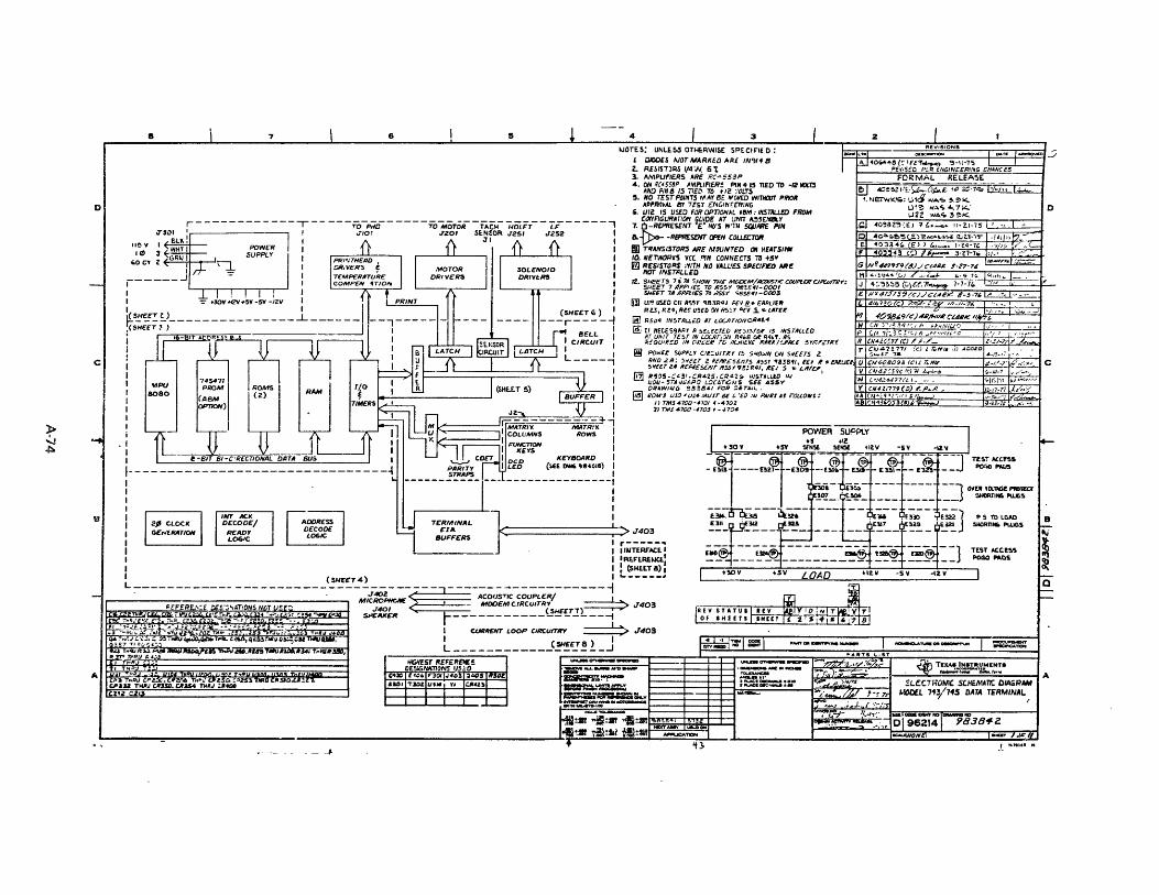
IS i 7
D
-
c
....
-
\ 6
ADDRESS I DECODE LOGIC
- ---I
I
T~RI"INIIL £IA
BUt:t:£RS
1 4 I 3 I 2 I O<~"'" -J
I
I
+5 .1Z
~ 40W44-~i~;;g-'~IVG/~~\~-;'~G CH!-:,A""N"'"Ce"'S,.4---f
=====FORMAL RELEA~E ~ 4C~~ZI;":~;a-;..£. ," ;C-7<i:, ,-'~",-,-,,,-, -'-*'=--j
1.NEiWK.;;,;·.J1&W ..... '.~I<. U~~ ."V~ -4-,7"-.'Wu WA .. ~~K
POWER SUPPLY I _,",,=-+='r.0="=""=-==+::r.5\'====-5f~~ !>flO! <IZV -IV -IZ~
-.1 ----~ -:~ ~,~.$:~r.~ uJ ~~: ,~-.- £~-t---l-~-- --] OVER'll.lMiEPIII1£C1' l~.!~ __ ij-~_ ___ ____ __ SHORTING PI.I.£!t
-;.;;-~---~-;;- --- -- .1-;;- ,E;;- ;~] PS TDlCAD
~~¢I_ ._~~~_ct.~ _ _____ 'E~7 __ I]£~~_I'~ !IIORTlNlOPWGS
;-.;-- --~-- ---------~ t~ -;;,~ --] TEST ACC'-!>'!; __ ____ _ __________ ___ __~ __ POQO MQS
·nov LOAD +I~V -5 V -42Y I
fREY STATUll UV~IY 10 1,. TIM'V Tl Of SHUTS SHEET!' 2 .'.,.!6'7!8!
D

o
c
> ~ U1
6
A
8
.-----'-"' .............. ~ .z -t--~"--... 5 -t-:,,--'"-"6-:c.....-
! C31~ n(-1.1
R325 ,'0% 9.0~K 10/0 '
I
i U:oZ I ~'<i - 7 LM Eo
R335 I. iK 1%
7
"313 R31Z
ez ~.8
6 3 2
~--------.,
~0fT II 1183841 ReI! A AIIO EAI'L,!I~ I
R323 11\
1C3\4 .1
10·'"
CR35Z
1'1351 loOK .1%
CR353
START r - ~QW~!i "'§!:!pPLY I UNftEGULAlED - -1-- - - - - - - - - - - ~
I DC [341 I IWOG I
REGUlATED OUTPUT VOLTAr.E5
R3OE. 101(
1'1301 b.8K
I . +I~V 40T I I [J40B~ T301
C3Z" .1
500 V
~ I
R~2.B 47DK
R304
1.5K
+ C~ 200
lOOV
REG SENSE
I I
I
I
CR3ZZ OliN SS389Zlu£SI3CZ
+~VR I .~,3Z/~OV ---------'------' ~
'- _ _ IN5711 I OVERCURREIH "'Em -= ,- - OuTPUT OVER VOOAGE ~N5E - - - -___________ 1-_________ _-'
TO~I09 (SHT r.) +5V
Ro7e) 21<
o
B
[\J
t ~< o

o
c
1'l!35 14.'7t( 1"1.
3 cw
• 2 R3M. , 100(
R35i R3!12 LOI( 1.15K
7
.,.. .1"40 +5V~~~--~~~~
6
1 CIS I R353'\,..]~-~V R~57 .... &20 .. ~ .iU52
5 4
1~.05 _ 3.0"1( ~358 loOK
r>-----~---4----_+-_4_--...l--T ~~pf ------------~~~--------~
3 2
REG .... \.ATEO OUTPUT VCLTAcg;'l
C302 ~400 7.<;V
IC301 I
ZIOO IIoV
o
E!.'T -
f.'v~_~(~' ~12" foY5 A
En.
£31'3
b __ ~~A.O nl6 E>:l 1 C
JC304~ 22 :5~
I n~1\
[lifo
3 lID 2 -sv El!."' ~sv
OR Lfd3Z0T-.5 0 £~. ~301 MC7905CP ·i~'.1 --
.::!1!....o __ ~-IZy~'.Itll0 tln t \
nzo E12! B
A
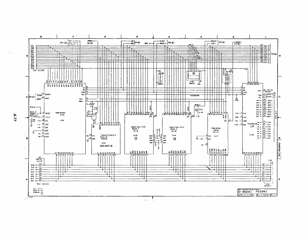
I P,,"
_510
e
+$V ...!!: ~CC
• .=, ~ 100
-SV -'-'- VBS
~GNO -= Ne -~ INTE
Nt~ HLDI>
TE~r AC.CESS
TMS6080 CPU
U15
7
INT
WR-
OI5lN "a
1"1
1 74.~U4
2 ETo!!
E~ DSru~[
1 z "14LS5Z en
, 15
~
+5~~ vee
IF &HI)
6 !5 4 3 2
I
I I
",I .ll,l, .. " :: AD AI AlA\ M MAAoAil
~
,4S411/1454: Z5~. 6 PROM
UIZ
~EEKOTE ")
f
+5Y 2 vee
GHC ....!.. vos ,
-5V - vee
1114 l'io ." 11 ~~ AOAI I.Z A3
SEN ~! .. JSH~) SEU'50R
TIIO ~1DAT"}~ Rt ~VOAT .:':3- C
U.8
OUTO ~~iZlRO-OUT I ~iZlRI-OUT 2 ~"'RZ-OUT 3 ~-;iJR3-OUT. 05-~"'R'-OUTS ~"'R5-OUT. ~"'Rw- -1 OUT T ~"RT- ~
IN 4
IN !i
IN w IN 7 B
'" ~ o
A

D
c
B
+5
R7 s . .,
744~5:
A
E7S £60
4 3 2
r-------------------------------------------, I Q .. !!1 J40}- I I • 12V VV\ >'0 P.U I
er, ~rzy -,zv ~ 3.311: ~,SIGIV"L I
(SH 5) °1 ~ls--15--14-.__, Lii:A:JLlFT R~~4 -= 'R':;LlO: ONL fiE' • JJ2~-ID·n) 14 r'RB'J5'f
,~-" 17 (SITS) 21( I "4 - I ) 15 OTR
I +::I~TA " :6 I ( ) 13 XNlTD
I ~I(!JIB-~ I I ~1 L..-75150 -VZ--..JS : ~ 12 6! I RCVOITT /I r-:---c>=--....=;.-<><" t--lf------~ _ _+_---_4 12 RCVO
I (U/8-~) U7 13 I J 31 - i, J 151B9A I h-"----'--I-+----4·1 COET
I LJI ~-L:-N~ ---------, I JUMPE:RS INSTAL lE:O 1 I ON PORTABLE • I I It 9 ",9 .1/ 9 UNIT ONL y
J I ¥ I i I ~ I (SEE SI-!T N'!) I I I TERMINAL ItHERFACE L~_~_~ _________ ....J I L __________________________________________ ~
+5V
CLlC¢2 l E:S8
PWRCLK ~~~g ~~-...:.:.:.:.::::;;~---<~- f"tvRCLY.
£20
t
£16
PROM-(LI7-l,SHT A)
CTLTSTRBE-
(UZ&-9,SHT ~)
CTL2STRBE-
(UIS-/S,SIIT':")
( '-'101 - 9, SHT
d;9 105 105 II ... lOV 1& Ie
ilis 1.05 ~5v Jc4
15 los 1s
I" II4 rl8
105 +-llY
TCI7=}
105 , ~5 JI9 ]'zo
TO CZC3 (SI4£~T i.)
--r--- +sv J..,::>5
'r21
~ ~-I2V .05
Tcs
~
o
c
B
A
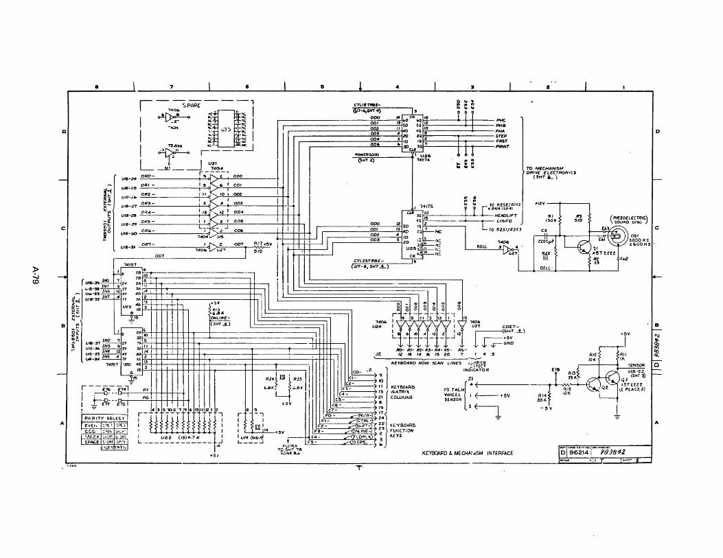
• 7
D
ORI - COl UIB-Z~
I~ Ule-a, ORZ- ooz
~! UI8-27 OR3- 003
)( Ie
0'<4- 004 ~ UI8-28
-i UI8-Z9 OR5- 005
01--C ... :J
"0 UlB-.so ORf>- 006
~ U18-31
0R7- I Z 007 R11~v
740f> (,2"7 010 ClD7
P~R'T A EvEr.
cc.c. .~t..~j(
SPAC.E
+51
CTl.ISTllaI-
l-.,SHT+) ODO 001 OOZ 003 004 006
•
~--------~~~---- P~ ~----------~~---- PHS 17-----------~---- PHA i~--------,---------STEP t-=-----f~--- FAST Ij-!--------t--i-<t---- PRINT
'" " "' .. I 1't17S '" '" TO RZ5Z/R255 r .. R4/4 (SH4J
WI 3Q t-;/v;;---------+~..l__ HEIlDLIFT
4~ f!:15c----------....... --_--- LllvFO
2
TO MECHANISM DRIVe eLECTRONICS
(SHT .L.)
~/ZV -~----------.
II. '!lOK
TO R251/£253 C3 r-____________ -=O~DO=__ __ _=i1Z 30 I~ 1-!2=--_. ______ ~
r-_________ --'~""~:..:..~----....:~'=-i3 40 2Q 7 NC
"
>--+-+-+--<i-----J r ________ --.:0:::::D=3 ____ ....:5~ ~c:, 1<) 3 • I I C~ i ~t~~t.j"~~~:--.J U2!i;g;~
I I CTL2STRB==~~-__._------.Jc~ I {~-.,~TLl
I
II II
NC NC N:: 1'1[,
'----==_....:~=-l"06 4~!tot:.pr IIZ7 7m2
8f~L~L-~ ________ +-____ ~
K~D &. MEOI.Al dSM INTERFACE
E6Z
OSI 3WOHZ ±f>OOHZ'
D
c
A

D
c
B
A
8 7 6
R'SnECT 2~1 TO L4IUl V~EF EIIIC-C~---""""'~:r
RIZl 0 EIU R~n.
RIZI +12 V
RIl'I! t..1'!Ift
.1Of.
PVFET5 CI2S~ 1 TIS·S o VOLlS ,T1CJI:" RI1~ ,cf"\,....,~,....'._-z ___ -'\NY __ +---=~
1'1'. 750K :; R1I9 -470
2
-1 CZO, .0'
E1I4<:>- 100 ~.
RIll ,,,ft:. RI07 I.SK
III. PHC ----+-------+-----'-==K I IN9.4!!
D~V'OI.6~ I £10" _
ZIS.n I f~~3
R StcPE 3~~:~--t---+----------' D-1SHOC JIO'-I t----.
£'O/~ .,,;-
GNDS JIO/-3 M--. C'O) ~ *"
PRINTHEAD DRIVERS
='"UO; eRIOl
RI05 21'1.
}--nJ'Ol-,~N.C;~T 5) PGND
-= £118 e214
2~~I -12 V TEMPERATURE
COMPENSATION ,-".~-jf----o EIIZ PVSWS
IN914B CRIO' 4.7 K
RI04
I PG FROM POWER
SUPPLY SECTION (TO C3~3 (4) ~HT 2)
>---t==---=:'::"_~J IOH7 £120
>-.L:=--...;.:c:-_~~'1()1_5 £105
1125-'5
-t5 V
F~T-----~~~~--~-~ uzr.-z @HT~
£207 C>o-Iw\<">O"T"S w=---'< +5V
RZIS IK
LIIIIFD -~"""''''''''_-H C·WT~
T
lC20Z .Ot
MOTDA t----4 ......... -+--_---<> E20,,"
£ZOI _-------.... -'),reol·I
MOT-R
+lOV
D
c.
A

B
A
• 7
-------------------, r IC4Z41~ l : __ ---4t_~~~ : " I McSm 11E~~ .I~'o I
~ ':" I I I I I 10K R"16
: ~~r'~-~~ __ ~~C~R~"~S4_~/~C~~~~~,,-.-I--.~~ lOll. ~"7A. 1
rIi II
$I '\I ~ II t i ~ t 0.0056 II I
10$ II 5IC3K5IC!K II
fi.iMITER---~Ir:'l I ,
I CR I I I I R4e I I I I I I 7 I
I I I , L ___ -= ____ -'
~ ---- - ----- ----, I I
: TO 1lECF:IVF: : I CURRf,NT LOOP 1 L ________ ~! ____ ~
R"5Z ~--+-+---......JoLI/I~I\/(----......... 7 ~:g::~
r 1,;r~A-; _-; - F:~S;
, INSTALLED ON : ' I I'ORTAIJtEIJNITONLYQ£40Z1 I SEESHT~. I L __________ .-l
2
+IZV--_-..,..,,~
4Z! ~D ----~~~~~~r+~
-
~2V-----~~~~~----
.. 'ZV
~
:
.05 (., PlACE~) +&0,. -20"
L ___ -- - ------ - --h-.l: ~~g.0A~ ____ -- I
I Ii!I+S -II I I I 1401. f{J$. :! 7 :, I I
L_ CIIRDET '>!.-+-_-.:.RV'40\II7~+--~ ___ ~ J403-2
1.511. ________ -,
FER';-;; . '! .'1' d I" U, I I
(SliT ~ " I II : C.~O, 1;,3 ':" I I I ':" - 20% -'ZV I
: 1 ~ _~"4 __ .::~...:_:.:.. __ --_-__ -_~ __ -_-__ -_J_L_-_-_-_-_-_-_-_-_-_-_-_-_-_-_-_-_...J--J I
r-- - - - ----R;;;;;------I I foIlV I I I
I I
I I I E41l I ITRHGWVI I I I I L-__ J~~-4------------__ --~1
FSK TRANSt.lITTER I ________________________ J
..
R430
S1_IK ,,.
C401 I .01
R"" 10.8111 1%
R410
'3_'1( 1%
1 I I 1
5 lJ4;S I 1
;£-:;;., : ~Z~~~1~~/~P£ : I I £401 JPORTABLE UNIT ONLY I I S£ESHT ~ I , I L ___________ ...J
o
c
B

7
o
C INO 31.t.1< a;~
~ » do I\)
liZ! .01
RI60 8.37K .11-
R·HI
B J/.,K
().I't
A
6
3K
4
fL iMiT£R - - - - - - -, I (R409 I I I I (R I
I R412 I I R4H 75K 11. I I 1.4K I I I"/. I
I I
I I L. ___ := _____ J
R410 '40'r ~3.11( .(N l:.c
3 2
r::---------, I THI5 ':.flEET npPLlES TO I
nssJ" 93384'-00[,3, I I..:~£.. ______ -l
o
c
B.
o
A

» Co eN
7
o
B
6 !5 4
t
3
r----- ---------,
I "'0 ll€CF"JVE"
• :Ufi'PO!.!,,_OCP R.'j. - ~ - - - - - - - - - ~
--'\1\ ~ RCVDATA
~ _ ...!~A ___ --1-'-~-;03-" l't"(~dll. :'.JMP[ R . ~ E 405 !h:;fA iff- -~: I
~~~~~/-}T' ~/~ ~N'-Y r r40Z :
____________ -.l
2
-12Y
'T7";,j -HiE-'- /1/ .. ,pi7F;; {O..., I !J':'.Y "f':-;"11-:;,,,4 I L __________ .....J
(425 ---+- ~
.05 (9 PlACi":) + 80 'Yo -ZC'l'o
o
c
B
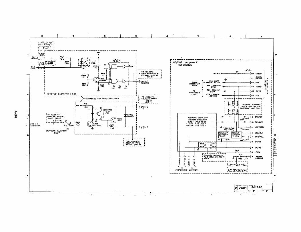
D
c
~ ~ 00 ~
B
It.
8 7
U4:l1 7!)·!);)P r----------,
!5
J'~~-78-~---<>----------~ 1IC7t~ +5\o':rl----7 V i·~ r---------...,
R4/6 II(
R436 10K
II I TO ACOUSTIC I
'II : COUPLER / MODE,'W 1 I I I RECEIVE OUTPUT 1
II! : L ___ ~"!.7L ___ -I
I I ::-..,.'..0...7 ------.-7 J403- 8 ""~---:C!:t-,-L---' 1 II.CVDATA
---T& ---B---YS.J +12 -:- -/2
i
~2~C~~~~~~~~-~.:~-"'=I~S_;,:~L~~~:;;:S~y-~~_;----=R---J i-~gu;z~iiiD-l r-L--------- ------------- ..., L In}~f J 1+
510' R401 I ---------
I ISO. 5 J403-':\ I r--- '--~--1 (XI ... ') I ).\
r-----------, I : I ;~~7 I ,70 ACOtr.:>TlC I I I l ~ CR403 : , COUPLER/MODEM' I ,I I INQOO3 : XMIT INPUT : L __ -t,r- oJ TlS99 I
J103-3 (
I • (51fT4+7 I UI I N~ " G40Z I f-___ L_-_-_-_-.. l-_-_-_-_-_-_..J= : 11.419 Q4C3 I
f() 6 751894" II( A 572222 I 'XMITDA"TA -I I 1..51(
TRANSMIT CURR!Nrc I : lOOP L _________________________ ~
J40:'-4 lZ.
r--- ----.., I TO RCCUSTIC. ! I COUPLER HrBPID i :... ~R.!.~_!!~.!~ ...J
4 '3 2
r--------------------------------------------..., 743/745 INTERFACE
REFERENCE
HDC.FTENI-----"~ .... ---~) I. CRlWSY .1403- 1 *,...--------7 I ~~~hD au
{
EIA DATA ..J~ ~~SOR TERMI"'"A£. RCADY - ... ---------)~ 15 OTR i~
LOCOIC EIA TRANSMIT ~ .... DATA _-----..-----;~/3 'XMTO j r.: <:
~-EIA D:i;CIVE ----r-+----··~? 12 ReVD ~
EIADi::frER
_-...... -+--+----~-) /I COET
TO { PROCeSSOR LO(i,IC
ACOUSTIC COUPLeR/ MOD£M CIRCUITRY
-0001 PWB ASSY -0003 PN8 AJ5Y -0004 PIIB <ISS"
r:t~ ~ -------'-i I ~-!I i ~ INT£~NAL JUMPf"RS I I .. I 141, lor, INSTALLED ON Sro. I I :: PORTABLE UNIT 01lL Y I I ~Q ~ I L~ ~l~ __________ J
r--~~-~-~_r-~~_72 CAROET
r--t_----< ..... -+---~-~ tI RCVQATA
D
c
It.
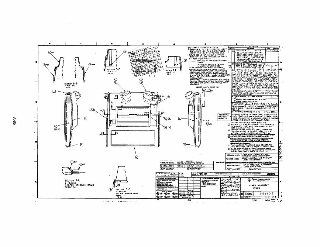
» Co (J'1
D
c
•
A
8
EJ
liAR
SUliON B-B $CAlE. III
1('6 )
SECTION A-A 2 PLACES
7
1!]9
I PLACE MIRROR IMAGE SCALE 2/1
fjf SCALE. 11"1 (c-61
2 PLACES , PLACE ",:RROR *"'Ie SCAU: 1/1 (B-"
4
~® -.~
SCAle. III (C-41
3
E]ASSEMBLE OUTER -::CVERIITEM I\L£FT $IDE INSERT liTEM ll.AND I?GI-l~ SIDE It&RTflTEM 3) BY APPLYING ~E SOI.../D BEAD OF SUPER BeNCEI<' 1~/lTEr~ I I) CLOSE TO EDGE OF PAI?TS IN IIIDICATED APEJ.S:
2
••••••• ~L~ES TO FAR SIDE OF INNER 1-+,-~':::":':~!!...:2"":':'::::::"'="::::::':":"'-+--+--4 ______ 'NOICATES FAR SIOEOFSIOE
SLIDE IN~~~Mcf~~ ~~~~~ER COVER. RIO('ES ON S.CE: I'lSERTS MUST lOUCH I'lNERCOVER lOGE. CLAMP 1/I'lER COVER AND SIDE INSERTS TOGETHER AT UNIT FIO.RT1NG LINE FOR APPPQXIMATELY • MINUTES TO REACh AANDLING STRENGTH, AND C.URE , ~R M~l1l/lJl\II BEFORE IN~AlLATlON, WARNING: SUPER BOtIOER '!SO BONDS ~IN IN SECONDS TO ANY SURFACE. KEEP I'IDHESNE OFF SKIN AND HANDLE WIT" CAUTION.
NOTES CONT, l!ONE B I
G f5HZ.C-81
•
:::..on::~ b"""'~'-~~"""'~ i~~--~.:.S£..· _T.!:==:,r&.;::.:IN::'-:..TR..,:*7L-=M:.,:K,==-"=--_-:t A
30
J""-'"'Ca~.O'O 2~~.a.
98380B


Item No.
0001
OOOl
0002
0003
0004
0005
0005
0006
0006
0007
0008
0009
0010
0011
~012
0013
0014
LIST OF MATERIALS
Assembly Part No. Rev.
COVER ASSY, WITH XMT LEVEL ADJUSTMENT COVER ASSY, WIO TRANSIT LEVEL ADJUSTMENT COVER ASSY, INNER, 745 JAPANESE
0983808·0001 M 0983808·0003 M 0983808·0004 M
Quantity
00001.000 EA
00001.000 EA
00001.000 EA
00001.000 EA
00001.000 EA
00001.000 EA
00001.000 EA
00001.000 EA
00001.000 EA
00002.000 EA
00004.000 EA
00001.000 EA
00001.000 fA
AR fA
00001.000 EA
00001.000 fA
AR TU
TI Part No. DeSCriptIOn
0983981-0001 COVER,INNER,145,ROUNO CONT PWR CONN
0999248-0001 INSERT,L~FT SIDE W/XMT lEV AOJ,VENTEO
0999248-0003 INSERT,L~FT SIDE wiD XMT LEV ADJ,VENTEO
0999249-0001 INSERT,RIGHT SIOE.VENTED
0983865-0001 DOOR,PAPER
0983826-0001 MUFF ASSV,TRANSMIT,ALDUSTIC COUPLER
0995610-0002 MUff ASSY, XMIT,OVERSIlE, W/STRAP
0983821-0001 MUfF ASSY,RECEIVE ACOUSTIC COUPLER
0995611-0001 MUFf ASSY,RECV,STANOARD,W/STRAP
0983875-0001 RETAINER,MUFF
0772334-0001 FASTNER 4-40 ON-SERT
0983913-0001 NAMEPLATE. INNER COVER
0983912-0001 LABEl,PAPER LOADING
0996521-0001 AOHESIVE,lOCTITE 416
0418212-0040 STRAP,TIEDOWN,ADJUSTABLE,PLASTIC
0983961-0001 PAD, FOAM 3 X 3 X 1/4
0417559-0001 SILICONE RUBBER (RTV) OOW 3140
A-87
Remarks
for ·0001
for ·0003 & ·0004
for 0004
for 0004

o
-
c
B
-
o ~I)
KEfif
z DJl' <) PLACES ~ Ail
•
r,_-----...--o _~I c
~ I
I
\ ~3 PLACES

Assembly
BASE ASSEMBLY, ROurliD PIN POWER CONNECTOR BASE ASSEMBLY, RECTANGULAR PIN POWER CONNECTOR
Item Quantity TI Part No. No.
01.101 JOO01.000 EA 09fl3C; 8e-OCO 1 0.101 00001.000 EA 098398C-OC02
01.1-.12 OOCJ4.JJQ EA 0983988 -0001
OJO 3 AI' GL ()235314-1COO
lH.lJ4 )0003 .. ;"0 EA 0972678-000 7
LIST OF MATERIALS
Description
Part No. Rev.
0983807·0001 C
0983807·0002 C
BASE-PRINTEP CASE ,ROU~ID PIN Po\~ER CONrIECTOR BASE-PRINTER CAS E, RECTANGLE PHl POIJER COrJrJECTOR
CAP.MECHANISM POST
SOL VEN T MET HYL ETHYL KETONE 99~ PPA
BUMPER,RUBBER
A-89
Remarks
for-0001
for -0002

D
c
B
A
~;.~~~;;~~~~:7~~~::~::~~:S~::~::~ __ ~::~S::~::~*~~~=-~4 ________ ~ ______ ~3;-------P~;;;;~;;~~~~~~~i3~~35 ~~l",,)h£s~;r~~~Yi'icr.J.~\f I), LUT III INSTALL PAPER DOOR (ITEM 4) BY BOWIN6 ~ USE SILICONE RUflflC" ('W..t M) TO m ~IDi 1i'I=i'~T (ITEM Z).A~D RIGHT SID( OR BENDIIV' AIVD INSERTIIV' STUt;)S INTO STRAIN RELIEYE CIII!JLE .!IY APPt.f'IN&
':lllTi'~U1Vf(/t:mN~L~:f Sfi'D HOLeS ON CO'l£ll "TEM I) rg~'tttm;,.f£.,.'t,.UItKf,f.T:I~E::/!/~'!c 7)
£D(.I OF Pil'lTS IN AlIO'i> INDICATED: !1: CENTER PAPER WADIIV6 LABEL (ITeM 10) •••• INDICATES A<'.~Lr TC FANSIDE OF ON UNO£lISIO£ OF PAPER j)()()R (/TEM 4)
"'''ER COVER wlTUIN :t.10 OF CENT£1l~/N£ OF DOOR ---.,ND,CATiS APf'LY TO FANSIDE ('F
INS~"'S (WITI/()(JT RIBS) 00 PULL LEADS OF MUFF ASSYS (ITEMS 5 SLlD£ 1 .... !iRT 5 IIVTO SLOTS OF INNER AND t.) T06£TliER AND SECURE' TO C~V£R. RIDGES f»J 510£ INSERTS MUST iACH OTHER /lSIN6 STRAP (ITEM 12) TOUCH INNER Cfl'IER ED6£. CLAMP INNER
£o:,f~~1fNt'~~t"io':~~ktKfxr;:J:r:[Y (lJ 't"l:f ;:if,i,ff1fisp~'t'~~J:gZ£R 4 MINUTES 70 ReACH Hi<NDUfII{. STR£Nf.TH. IYAMEPLATE, INSTALL IT IN PLACE CURE I HR IIIIN B£FDI/.£ INSTALLATION. OF THE STANDARD NAMEPLATE (ITEM i;)
WARNIHr.: ADHESIVe f1TEM II) BONDS S/(IN TO ANY SURFAce IIV SECONDS. KEfP ADII£SI~E OFF SKIN AND HANDLE wn: CAUTIOlV
Pltor.r:~s
E'ii~r _H:JIIoC
--.. !.- 6
B j
,,,uo an. ..... us«o
4 30
file SH;-'1 (A-I) I
e.J
"923' -0006 COVEIf ","y. INNEII 745'. ~,:s . ~ 999239-0005 COVEIf AlSSl'!,INN£1I " ",,, ~UZ"'OO04 COVER AS Yo INNER ?II r. ... A , nrl9·0003 COVER ASS~ INNEIf, 745/7(,$. W. (NfIT ,j/)'/ucr "'239-0001 CUt'EIf ASSY,INNEIf,7"15/7t.5,'II/rlllr-.iilJUST
D
c
•
A

» cO
c
B
2. REF
SECTImI A-A 5H' «(.G.)
I1X0 R[f~ REF
~
[Hi4 AR VIEW C-C :IJ 1([-3)
8 2 PLACES
3RfF
8 2PLACES
SECTION B-B 511' (B-to)
f
o
c
B
A
A--.ey COVER AISY, INNER-7_, W!XMT ADJ COVER AllY, INNER-7_, W/O XMT ADJ OOVER AISY, INNER-7_, JAPANESE
IUrn au.ntity No.
0001 00001.000 EA
0002 00001.000 EA
000] 00001.000 EA
c)OU4 00001.000 EA
0005 00001.000 ~A
0005 00001.000 EA
0006 00001.000 EA OOC)6 ooucn.ooo EA
0007 00002.000 EA
OC)c)8 \10004.000 EA
0009 00001.000 EA
QUI0 00001.000 EA
0011 AR EA
OQ12 \JOOOl.JOO EA
0014 AR TU
LIST OF MATERIALS
TI Pert No.
0983~81-0002 COYER. INNER-PRINTER CASE
Pert No. R •• ,.-z»OlO,D ~D II1II2»_ P
0999248-0001 INSERT.LEFT SIDE N/X"T LEY AOJ.YENTED
0999249-0001 INSERT.RIGHT SIDE,YENTED
0983865-0001 OOOR.PAPER
0983826-0001 MUFF ASSY.TRANSMIT.ACOUSTIC COUPLER 0995610-0002 MUFF ASSY. XMIT.DYERSllE. W/STRAP
0983821-0001 MUFF ASSY.RECElYE ACOUSTIC COUPLER ...... , .... 0995671-0001 MUFF ASSY./RETAINER-REC-ACDUSTIC COUPLER .. ~
0983815-0001 RETAINER.MUFF
0112]3~0001 FASTNER 1t-40 ON-SERT
0983913-0001 NAMEPLATE. INNER COYER
0983912-0001 LA8EL.PAPER LOADING
0912799-0001 ADHESIVE SOLVEHTLESS RAPID CURING
0418212-0040 STRAP,TIEDOWN,ADJUSTA8LE.PLASTIC
0417559-0001 SILICONE RUB8ER (RTYI DOW 311tO
A·92

•
D
C
\ l> I'. .210DIA
ch' 2 HOLES
W
•
A
7
375~
.188 I F
IS
l"SO
VIEW A-A OPPOSITE SIDE IDENTICAL
(B-4}
+
7.250 --------" .,all
4
A .12DDIA l 2 HOLES
0
=i
--........... --~ ..... ~~
J A (c-ro)
3 2
D
03
C
•
c

8 7 6 !5 4 3 . 2
o o
~ VIEW 0-0
C OPPOSITE SIDE IDENTICAL C (B-4)
» eO
SECTI\Jf'I [-L ~ 4- PLACES
~C~~~.o,i, (~~~f 2 D
l B •
e ~ 0 CO ,.., CO m
0
J o (C-6)
A a ~ (r i"n=,i,~
A
SECTiON B-B 2 PLACES I MIRROR IMA(lE SCALE 2 I B-5 "-'cOF2.
FII.Illr,

Assembly OUTER COVER ASSY
Item Quantity No.
(llllll 410;)01.000
0002 00001.000
00113 00004.000
uOll5 ,)0002.000
01)06 aOOO8.000
Oul)7 IhlOIl2.IJOO
oooa J()oa2.II0a
TI Part No.
EA I)Qa39aZ-0001
EA 0972449-0001
EA 0983Q01-0001
EA ,)418600-01<;0
EA 1)4180/)6-0,)35
EA 0972447-C001
EA 0972448-uOO 1
LIST OF MATERIALS
Part No. Rev. 0983109-0001 A
Description Remarks
COVER,OUTER-PRINTER CASE
HANDlE,CASE-CARRYING,SOFT TOUCH
LATCH CASE
RI VET .188 X.407 TU8ULAR,C'SINK HEAD
RIVET .123 X.375 TU8ULAR ,C' Sf Nt<. HEAD
CAP,PUSH-oN-HANOLF
RETAfNER ,CASE HANDLE
A-95-

» cO 0')
D
c
8
A
s
I IIU
10 AR
stellON B-B SCI\\.[: III
(c" ,
SECTION A-A 2 PLACES
7
I PLACE MIRROR IMAGE SCALE 2/1
C (A 6)
6
r A A LrP------- ____ n_, ):
i ; : , ________ - I
4 3
NOT£S UNLESS OTH[RWlSe 5PEe/nW:
UI'IIlLUO.., .... ~~'O
~.AU. ....... AIC) ........
C/:JN'~.lotC ....... ~ O"U'Ohf!i:>{.OIO ....
()IIo.-. ';:"UIo.LL_TS~V 1I,>-y. .. J. ..... _~ .........
1OF·"l-.y ..... t.~SHO¥IIN .. P'_u.rn, ~ ... SJ.QIIIMf'VdNCCOf&.V
~'""""CI"IAWf'IIII .. ~
[Q ASSEM8LE OUT~R CCI[P (iT£IJ r),l[F T slOe INS(RT (I,~,\.;''l:' .J~\L(,4rf,)~r- ,·,:,[I?T(17Dlf3). BY ~PLYI':, r !: " ;. IJ (J St,r[(? P/·.nn~ 150(Jr£f.f - -~, :. Til !'. or r~1f~TI'" '''',l7fO AR(AS .... / ' .... ES 1 IS' -: OF j, ,E..R CC-VER, -----INOICAT£.S F "7 - r, sc .... I ',':RT:- (VIITHDUr RI85\5L!L'~ Irs J";lfl )Wi"l (, ~'~ ,-r.[R RIOCf..') 0'1 r -rlns "J'JT ltiU(H , ~I~ C!hl[R [OGC CLt·~ e; .! P' :R AND '",'~[ "S(PT5 TLJ6ETHER ,;- ,. ;;J~" '; l - r ? A,-/l0I)XH11\TELV .f.MIMlTf5 \' ,'If:i.' ,'rl.·, ... ·,[~d 15DBDJ,C5 SKIN INS£COI [,5 1 [, '" ' ',,--AtE, HlP ADHESIVE OFT SKIN AND HAND:"t I I 'i l~ 'ION. -NOTES CDNTI~VUl ZONE 8/-
2 1 .
1)16h ... l' '/5 11f.;lUI) IrEIV' II
8 ~m(;)~-;:-(~A-zrtO ~UI;-~ /JF-CN'l-Z9YI-3{[JC(J!!,'L",A/J ,1/ ICoN /(0
C £)£/)('1( -of u:;r JIIA;ItJf. 1N1[IIiATICIIW.. 0 (;.) JrDDrp W17J1 7J''',,<),J'- ADJ T(,rl Allu I) 0,;1"
, ./16 7fl"}IIT ~~I r;., ____ /-13-78 <I" II /1 D ir1:lz~{3;(~~)~:)--~fi3~1~7f-:;~~~tp,~ /
-~:()' ZN:~: LM9;i£~~~~/,,'L~E. 3_1,,-1, .L..~
IolO'TES' ('O"""'U~!) rROM ZOI..E. ty~ lIl'IolST~LL (I'TEM 4) '1.110 (11E.M I) e.'1 e.0\N11oIC,/
e.E.~l)INu(l1EM 4) "1-10 IIolSE.:HIIoIC, SI'U\)S IN10 HOLES OF "E.M I. m C.UI'TER PA.PE.R \.OA.l)ING LA.l!>EL(11E.M 10) ON U"lDE.RS'DE. OF P~P,-~ DOOR (11£.M 4) \0111 .. ,,,, !. 10 OF C.OIH.R LlIolE OF (11£1'14)
III If TH£ 5.A.t(S, ORDER CONI=' ,G.UR .... 'IOt4 ~HHT C)P(CIF"i'~ A ~P[CIAL CU5TOMERS flAME Pl~T£. 1"l5TII.ll n .. AT PART
IN PlAtE OF IT£M e.
CDV(R ASSY, 7-f3.W/t> TRANSU"M
coveR ASSV, 743 W/7H TR4A1SMIT;/AftIS
D(StRIPTION
c
8
fR co· r<) <D (j)
Q

LIST OF MATERIALS
Assembly Part No. Rev.
743 COVER ASSY 09831159-0001 0
Item Quantity TI Part No. Description Remarks No.
0001 00001.000 EA 0983991-0001 COVER.INNER.7~3.ROUNO CONT PWR CONN
0002 00001.000 EA 09992~8-0001 INSERT.lEFT SIDE W/XNT LEV ADJ. VENTED
0003 00001.000 fA 09992~9-0001 INSERT .RlGHT SIDE. VENTED
0004 00001.000 EA 0983865-0001 OooR.PAPER
0005 00001.000 EA 0983931-0001 ADAPTER SWI TCH
0006 00001.000 EA 0983932-0001 COUAR. SWITCH
:)007 OOOO~.OOO EA o 71233~-0001 FASfNER ~-~O ON-SERf
0008 00001.000 EA 098.3913-0001 NANEPLATE.INNER COVER
OOOq 00001.000 EA 0983912-0001 LA8EL.PAPER LOADING
0010 AR EA 0912799-0001 ADHESIVE SOLVENfLESS RAPIO CURING
0011 00001.000 EA 0983967-0001 PAO.FDAM .3 X 3 X 1I~
A-97

o
-
c
B
-
A
8 \ 7
NOTES' {j,"L£55 O,'!ERNl5£ 5P!CIFIED
IT: AS5~', 'E_t ~ _ T[R (:'y[R , -U .. l 1', cUT S:;£ ',5t;;;7" (~£ .... ; Z),tNT) ;'I(;,~T S j£
~~~~;~; ;~~l/,~C (~T(~~ ;/~ .. ~ _i~j Z~.~/D E:::£ :1-- F:'ii T3 't J.ji£A5 .~,:':'''''f:J· •••• \~'ICATE5 ":'~;J ... Y T~ F.:.r(E;i CF
INNER :ellR ----II .. JI:;,;~5 ":'';;;LY TC FA~51DE. O~
INS;,O"(TS ,I: ,TdCUT ; 35) SeiDE ,'.Sf"::' ',TO SLD'S CF '.NER CO~:.-R ;;.C'{'E5 cr. -;,J£ ,5£;(T5 I/JST TLl[ (H '/;R [[I[k t.=G£ [_A~AP ,','VER c,;v=~ ".~ :: ~..,=- ",S[:{T5 n::'~-I..,;i< .:.T UNIT PAlC, c L/~E FOR f."t'fiJ1IMATELY 4 M:fo.UTES ;0 R,;'::'I h/''vJ.,,',G 5-;;:,\{'T'I CJ;r ) >1;< 'r1 ' .. ==:-:;;; I \51~_LAT'C~.
WAI?r.IN6· I.:"E;,VE IT£,',~ 1/ =;',:;5 SKIN TO A/I; Y 5Ji<;At£ ',S; :tNCS kf£F ADHESII'E CFr:- Cf: SKiN I.NO ~A'.:;Lf WtrJ, :':.JTICN
I 6
o INSTALL PAPER DOOR (ITEM 4)BY BONING OR BENDING A'VO IN5£RT,N6 STUOS INTO HOLES ON COVER (TElA I)
~ CENTER PAPER LOADING LABEL (ITEM 10) ON UNDU?StO£ (j~ PAPER ;;';OP. (:TEM 4) WITHIN :t.IO OF CENTERLINE O~ OOOR
o IF TIiE SALES ORDER CONFIGURATION Sl'fET SPECIFIES A S?£CtAL (&5T':M£R NAMEPLATE, iNSTALL iT IN PLACE iJF THE STANDARD NAMEPLATE ftT£M 7)
A SIl2
L'7l
I 5
A j
I
, I ~
/' S ::~--=-----=-~---=-----~-----'·~I ~ ~ ~ 1/,-... ...':::======:::91-- \ I "@1J
t:ll [I ] J
\ HOL..ETOLER .... NCE
4 I
n1i~~~ TI--~~:~r n~.£~;~ ~c:_ .... L9 ~73e
3
!
REVSTATUS 1m lelBI I I OFSMEETS ISH 11121 II
~~~~ i~~86? ~:f;· /'1 • '~~.::.AT~~:'l! ,. :50
I 2 I
c
B
2200044 -0002 COVER A55EMBL Y.- 7f3/">i>?, ----~
WITri XMITI10JUST "'" 1-2-2-0-0-04-4-_-0-0-0-,-I----:C:::-O:-:-V£::-:R:---cA-,-S-C;c-E-=-M:-"!.BL'..!.Y!:'.·~14~3'..!../ 7';3 g
WI,riour XMrTfiDJUST 0 PART NUMBER DESCRIPTION N
~ o
t-t--

» cO (0
8
D
c
8
A
2 REF
7
SECTION A-A SJ./ I (C-IP)
6 5
B 2 PLACES
SECTION B-B 51-1 I (8-1P)
4 3 2
D
c
B V .". o o o C\J C\J
C
A

Assembly
COVER ASSY, INNER - 743 W/O XMIT ADJUST COVER ASSY, INNER - 743 W/O XMIT ADJUST
Item QUll'ltity No.
0001 00001.000 EA
0002 00001.000 EA 0002 00001.000 EA 0003 00001.000 EA
0001t 00001.000 EA
ODDS 00001.000 EA
0006 00001.000 fA
0008 00001t.000 EA
00119 00001.000 EA
0010 ')00c11.000 EA
0011 AR EA
LIST OF MATERIALS
TI PIII1No.
0983991-0002
099921t8-0003 099921t8-0001 09992't9-o001
0983865-0001
0983931-0001
220001t0-0001
011233+-0001
0983913-0001
0983912-0001
0912799-0001
D-=ription
COVER 71t3
PIII1 No. Rev. 22CICJ044.OOO1 C 2200044.0002 . C
INSERT,LEFT SIDE via XMT LEV ADJ,VENTED INSERT,LEFT SIDE V/XMT LEV ADJ,VENTED INSERT,RIGHT SIDE,VENTED
DOOR. PAPER
ADAPTER SWITCH
COLLAR, SWITCH
FASTNER it-ItO ON-SERT
NAMEPLATE,INNER COVER
LA8EL,PAPER LOADING
ADHESIVE SOLVENTLESS RAPID CURING
A-100
Renwks
for-0002 GIlly
for -GOO2 only

o
-
C
~ -0.
~ -B
-
A
NOTES. UII.'I-ESS OT;'F:RWISF: SPECIFIED
IT] COLOR (8:AC'<, TYPE: to OR \~HITE, TYPE: 9) Slf4LL CONT"ftST WITH COl-OR OF IUM 2 OR ALTERNRTE IT[M 5
~ \\'(R~S S'-IALL BE CR MPE:D IN COM'I10N RECE:PTACLE PE:I? WIRE: LIST REGUIRF:MEATS
5 1 WIRE
NO
I 2 3
4
DESCRIPTION
MOTOR MOTOR MOTOR
BOBBIN 1-£::1{ I P25"l-1 I ~
I RED P252-3 / ~ YEL PZ5"l-6 /
@] rEYING PLUG SHOULD BE I'>!STALLED SUCH "TY/l"T ~E£PER PRO. EC"TS THRU h1E RPPROPRIATE SLOT 'N THE HOUSING AS SH(>WN IN SECTION A-A
... ALL "'A.T£RIA!..5 ML'ST MEET VL REtlUIR£ MiNTS
" MOTOR
5 MOTOR Eo MOTOR 7 MOTOR S MOTOR
~OeBIN /- YlHT I P252-S /
~:-El'N2-BUC,!PZ52-3 /}
• ~:~ ~~::; : (gJ BCf3BIN 2 - WH'r nS2-4 /
- I P252-2 " -
PIN I ~ ~ F38t'Z5-&6~~::::-==n ,_~, . r: ~ A
'0-MAkK PER PRocess ,
: AY. lPl~'~~A(B_7) ~ ~ 2 IlPPROXIMI4TElY WIiERESHOWN 'S=p' ___ BBlN / 3 5 REaD
4~
.1R£F _, \~
/ IMARK I 100-07 100 I III $10 IOI.IIIT 'mc... ADOfTIOfW.
SECTION A-A (C-7)
SCALE: NONE (ITeMS 2, 3,1-4 ONLY)
I
f
PLUG
30
A C/>/429301(/)),( "'.v"_ (11]);1./ tOO! 25 W,4S 738 ~./Z
LM
o
c
B t-.0 ~ o o o N N o --

LIST OF MATERIALS
Assembly Part No. Rev.
MOTOR ASSEMBLY, 4 PH STEPPER 2200045·0001 B
Item Quantity No.
TI Part No. Description Remarks
0001 00001.000 EA ()999256-0001 MOTOR,STEPPING PAPER DRIVE
0002 00001.000 EA 0912~84-0006 CONNECTOR HOUSING 6 CONTACT
0003 00005.000 EA 0912104-0001 CONTAcr ElEC-LOCKING,.[RE-TO.025 SQ POST
0()04 00001.000 EA 0912599-0001 KEY,POLARIIATION.CONNECTOR
0004A ITEMS 2,3,ANO 4 CAN ONLY
00048 8E USED TOGETHER
0005 00000.000 EA 0112701-0011 RECEPTACLE,TERMINAL- 6 CAVITIES
0006 00000.000 EA 0912482-0006 CONTACT,ELECTRICAL,CRIMP
0001 00000.000 EA 0800335-0001 KEY,POLARIIATION,CONNECTOR
0001A ITEMS 5,6,ANO 1 MAYBE
00018 USED AS ALTERNATE ITEMS
0001C FOR ITEMS 2,3.ANO 4.
00010 ITEMS 5,6.AND 1 CAN ONLY
000lE 8E USED TOGETHER
OOOd 00000.100 FT 0912436-0012 INSUlATION,FlEXIBLE
A-102

• 7
D
c
J.4EX~ Tit I
6 "-4Cl1ll/4 PH r PlACES
" []li)
•
A
\
.30
BI -0002. ·,TtJT~. O'-'E'" 8 I - I .. - &"1
DEscaIPTI~
2
CH"l411~~(c..)Cu-'I"'~/'JADD~D I o A TO "I'D ell A£)D[O CASu NO ~ ell CHATtO • Z LM
-""""""-
FUll lM ........ It
c
o

Assembly
MOTOR, DRIVE-PRINTER
Item Quantity No.
0001 00001.000
(J002 JOOO1.IlOO
0003 00001.000
0004 00001.000
Ou06 00002.000
00")7 OOO'J2.uI)O
0008 00001.000
TI Part No.
EA 0983813-00C1
EA 0983814-0001
EA 0983870-0001
EA 0215505-0001
EA (')972988-0013
EA 0411101-0051
EA 1)418212-0040
LIST OF MATERIALS
Part No. Rev. 0983812-0001 D
Description Remarks
MOTOR,WIREO
SENSOR,FEEDBACK WHEEL-MOTOR
CAPSTAN,MOTOR
W"'EEL,FEEDBACK SENSOR
SCREW 4-40 X .250 PAN HEAD CRES
LOCKWASHER f 4 EXTERNAL TOOTH CRES
STRAP,TIEDOWN,ADJUSTABLE,PLASTIC
A-104

4
-t
! }
c
r-
.n
~ ,
~l ~ril - ..... 0 U1
1-.- ~
L"~
~ 7 Aft
B I I
~ I
-•
A
I
I t
44-4QXI-I/Z
Z
3
_ _r=-1
.[J~ ---~
I~ I
.lw 'n -------
lurn
2 1 . ~ .. " 'N01E5:'UHL£SS OTHERWISE SPEctnED ~.."...--.. ____ ~=-:-R,:,:E-:V_IS_I_O_N~S __ --;r--:::-:-::::-T~==i m CHEC~ THAT NO BINDJNG 'OF ZONE LTR OESCR,P'ION D .. TE ........ OVED
lltt SCREW (IT. 41 IN THE /14. Ry/;,J!.o....J ]-21'7S r:::LJ-BRACKET <IT. 3) OCCURS TKAT REORAWN PER ENS. DEs/aN ~,,~, ~~ WOOlD ALLOW THE SCR~W TO CHANG£ BA~t<' OUT StroRC THE CARRIER .B CN429299t'C)~ //1 ~t:VIS~D (IT; 6> TONGU£, sOUows PICTtJIUAl.. ANI) N1J7£ Z t'2JADPED III /J II 0 OUT AGAINST THt SLOT END. ITEM 7 t·/1w1, ~ j m ASS£M eu 'EN SOR "l£M I)'
:.. TO CARRIER (Iff"" 6) wnw IlTlM 7). CLAMP IN POSITION AS P(~ METWDDS INSTRUCTIONS. A,l.lDW TD CURE 24 HOUR~ .tto~ IN!!tTAU.IN& liN H£II.T A5SY"
,..'
- ..... :=1 3
PARTS LIST
c
B
~ TEX,'. INSTRUMENTS
'''4. 1Hl1HI."'. 0 _____ 1_
A
Assembly
SENSOR, FEEDBACK WHEEL-MOTOR
Item QuantIty No.
0001 00001.000 EA
0002 00001.000 EA
0003 00001.000 EA
0004 00001.000 EA
0006 00001.000 EA
0001 AR EA
LIST OF MATERIALS
Part No. Rev.
0983814-0001 B
TI Part No. DescriptIon
0983820-0001 SENSOR
0960117-0001 SPRINC.FEEDBACK S~NSOR
0983920-0001 BRACKfT.MTG-FEED8ACK SENSOR
0912988-0023 SCREW 4-40 X 1.50 PAN HEAD CRES
0983919-0001 CARRIER
0912799-0001 ADHESIVE SOLVENTlESS RAPID CURING
A-106
Remarks

1 I 2 .·_1 629<t:.<a6 81 1 • IllVlIIOHS S-
lTl I DUCllmoN I DATI I APfII
A A
6.50 !.2 5 -- 03 - ~
L
V • f. 11l • [
I
LOWER SIDE I I I I I
~ - -+ .... 0 ......
I t I I
C I ~ C l....--......I
r--~--~I---OOQ--_I_~II~~~.~ 1~~ISIU~IT~~~::~I~I~p~~_N~WWN~R ___ ~I _____________ ~_K_._m_ON~ ______________ ~l_v~ _____ P~ ___ ~ ____ ~~ QTY~EQD I LIST Of MATERIALS
-t-_---:;U;.;.;N;:;:LE;;:;SS;..=.OT;.;.;H:=;ER;.;.W~IS;:.E...;:SPE;;,=.:C;.;.;IFI:=;ED=__ _ __1 PROCESSES ~;::;~".'!i!NO~J. __ tSl_ZETQj;=;W~i =~-----1~I~~"'~"D~/~t.~~~,.~ZJ~S 8/-_"'_'2/--l~ 4P TEXAS IN ST RUM EN TS
DECIMAL .XX:!: 02 XXX:!: .010 I 873Z 083833 INC 0" .. 0 " AT •• fRACTIONAL:!: 1/64 ANGULAR:!: I 0 ~:;'-:;;";;;;' __ ~-+-~/~="'="';=-----fC:;;:-..8·/~-7S DIGITAL SYSTEMS DIVISION CONCENTRICITY MACHINED DIAMETERS .004 TIR SlO \ <:> ~3 6 3 3 '1... ;,#~/C HOUSTON. TaXAS
:~~gtv~E~~°:U~R~OA~DM~A:~F~~E~ATING So s:7~8/~!;.lU PRI tJTHEAD, AS S Y D DO NOT SCALE THIS DRAWING v" t-------~-+-------------I~I .. =!'r~, :;;IJI!IIII~I_~. ,::q Ifin-W",q .,-.. __ ,.....--------------------------1 ALL DIMENSIONS IN INCHES ~ .Ast'" ...... SURfACES MARKED ./ TO HAVE _ L 'IlL' I
DRILLED HOLE TOLERANCES J.-------~+----------..J::II~~"1~7'.d·;,r 7W'11\ 1m ..
013 TO .I~~ !~D Aaov~3~ T~5250 : :88~ k:J2'..I.J?i~rFuLL' B' 983829 ,_.
D
I

Asambly PRINTHEAD ASSY
Item No.
OUul
0002
Quantity
UOOul.000
00001.000
EA
EA
LIST OF MATERIALS
Pm No. Rev. 0II3I2S-0001 •
TI Pm No. Description R..-ks
~q8383O-0001 PRINTHEAD ASSV RESISTOR SELECT EPN 2-1
0983922-0001 TAPE.DOU8lE SIDED PRINTHEAO CABLE
A·1OS

4 I 3 ~ 2 I 1 .s-REVISIONS
WlRlN6 LIST NOTES: ZONE LTA DESCRIPTION DATE APPROVED
OJ COLOR (JucK. TYPE 6 OR A 4095'11 (C) 1 ~.__ IH!I-15 lO--WIRE. UO ~TIO~ COMP CONN CO .... CONN REtMRN ITEM NO WHITE) TYPE~) SHALL CON- c-~ I) DIM,lo.l(:ft~O"WA5 IO.lChld', 414''5'
START STATION FMSH STATION TRAST WITH COLOR OF' ITf:.\A4. C:~ i) ADDED DIM • 2.0"! .ld".-
I ~AN MOTOR 81- !lIED P30C-1 I ~ SUPf'OlfT SHAFT Of ITEMI e 4/5530 (0) f)/.~ 7-/4-76 ", ... ~/", ~
0 ~"'DDEO I"TE.M'" 4 "-JO'Te ~ 2)ZIJ c-2 .20 01 .... TOL. W"",~.dI PINS lAND! WHILE INSTALLINt:, ITEM Z. 0
t F~ MOTOR B I-BLACK P302-2 ARl INTER- I [jJ USE ITEM 7 A.S N£C£~SA~Y TO 3 FAN MOTOR B 1-5HIELD P302-3[~] C.H~6U.LE I CONTAIN lOO!:.r. STRANDS OF"
f!5RIlID.
4 e.. [1] 1 .3 3R£QO t!i -
- ~OlO±~~ C
~ r- 10.10' :'2.6'
I c
PIN I
0 0 AR(}]~IO= , ~
-1-.50 MARK APPRDX --. ZO -.20
--+ WI-£R~ SHOWt-l PER
+-PROCESS I
f.-l(l t\J
aJ (I"J
aJ (f'1
B -U f.-
B
- f.-
1 ·2 1 ·1 liTEM I CODE I PART OR IDENTIFYING NUMBER I NOMENCLATURE OR DESCRIPTION I PROCUREMENT
I QTY AEQO I NO IDENT SPECIFICATION
I PARTS LIS T
UNLESS OTHERWISE SPECIFIED UNLESS OTHERWISE SPECIFIED D~~ .• OATE
~ TEXA~,! !:Iwl!!Rf!.Y!:' ENTS Z7 Mk(l!J
REMOVE ALL BURRS AND SHARP EDGES -DIMENSIONS ARE IN INCHES
C~~4: "-1L.-7'-Equlp".."r Group D.II." ru_
- TOLERANCES • CONCENTRICITY MACHINED ANGL.ES * 1-
DIAMETERS 010 FIR 3 PLACE DECIMALS * 010 ~ r./ ~~_?_7r • DIMENSIONAL LIMITS APPLY BEFORE 2 PL...ACE DECIMALS * 02 FINISH PROCESSING
A • IDENTIFYING NUMBERS SHOWN IN Q~L. !-7·f, A PARENTHESES FOR REFERENCE ONLY FAN ASSE~BLY • INTERPRET DRAWING IN ACCORDANCE ~~ ~ '!,-)'Jj~ WITH MIL STO 100
I MARK \100-01 710 rn HOLE TOLERANCE C~~':: ~, _A./I.'J!5 ~r~;N~~ ORAwlNGNO
SEa IDENT I F"-SPE.C loll ADDITIONAL T~:~~~ T~~= T~~= 983801 8732 ~V./I'l~EA}'.t6'A.r 383BES NEXTA5SY USED ON
NO ~ t.LASw:-ICATlOt.l Tr~:!:= 1~:!:8A~ i~:&\f APPLICATION SCALE 1/1 I I.:v 8 I SHEET , .
5 i LM FlMEl

As.mbIy
FANASSY _
Item Quantity No.
OOal ~OOOl.OOO
0002 OaOU1.uOO
0003 00003.000
0004 000U1.000
000 itA
00048
0005 J\)OOI).OOO
0006 000;10.'-100
0006A
00068
0006C
00060
0007 AR
TI Part No.
EA 0972486-0002
E4 a972489-0001
EA 0972104-0001
EA 0972"8-rOCl03
EA 1)972482-0006
EA 1)772707-0034
FT 0"17177-000"
LIST OF MATERIALS
Part No. Rev. 0983125-0001 B
Description Rem .. ks
"OTOR,FAN 12V DC
BLADE,FAN 2-5/8"DIA .078 BORE CW ROT
CONTACT ELEC-LOCKING,WIRE-TO.025 SQ POST
CONNECTOR HOUSING 3 CONTACT
ITEMS 3 AND 4 CAN ONLY BE
USED TOGETHER
CONTACT,ELECTRICAL,CRIMP
PECEPTACLE,TERMINAL- 3 CAY IT IES
ITEMS 5 AND 6 MAY BE USED A
ALTERNATES TO ITEMS 3 AND 4
ITEMS 5 AND 6 MAY ONLY BE
USED TOGETHER
INSUL SlEEVG,ElECT-HEAT SHRINK INDIA.125
A-110-

A
-
B
c
-
D
, f I 2 I 4 WiRE ~I " I "' NO DESCRIP110N ~~i 51GNATURE SIAR1RNIS:· REMARnS itEM ~DiE5:UNlE55 OiHERW\5E SPEC-IRED IIfVISiONS t-'
-0001 ~~I 5i A 51A 1'0 (I]CABLE CLAMP SCREWS ANO t-::--r-�-----=--------~----r---I I ccA'v\G IPVCVYH\l( 3.0 IlMTIHMITDA1A PH3 PI-:) J\.lMPlR ON p\ 4 REiAINER CLIPS AND SC.R£W5 rl.:.;;TI-+ _____ DlSC:.::.:=IIPT1O~N_=__ ____ _+....:D:;:ATI=-...j.I---=APPD==__:__I 2 22 AWG 1P\CVt'H\1E3.0!~"D-RCVDA1A PI-IZ P\-fl JUMPER Ott PI 4 INCLUDED \NllHG1~M o· -A.J40G446(£) !lkN;J).?PS 10/t??/75 ~hq,hJla-i~ 3 22 AWG IP'l: WHilE 3.ilILDEI-CARDET PHI P\-2 JllMP£ROt(Pi 4 [?J RETAINER C.L1P IN51ALLED WITHt---rA_D~'N.~'D---=-1):........;.Ir._£_M--=-5 ______ ~-:-_...--__ -I
-0002 THREADED HOLE ON~AME is 14D9BlO(E) .." 1"' 11-~-75 0./4,/,,1 .... _ ' A ~IDE AS SCREW HEAD. ~ '-' LA.~"T , ~- ---
I ZZAWG IPVC WHITE' 3.0 XMTD-RCrD PI-13 PI-Il JUMPE£ 4 @]SC.REWS MUST BE THREADED I) ~ODEO NOTE GJ Z 22AWG IPIC Wl/lTe 3.0 DTi-WET IPI-151P1-IIIJUMffk 4 C.OMPLETELY THRU ~iAINE.R z.) ADDED I.D'· 'TDTAL LENGTH TD WIRES.i 1 Z +3.
c.L1 P 5 r::-1) ) 2. PLF\CES:i\ 3) OM F/D~ ADDEO ~ AND DUTU NED PIN -REV AREA 0'1 rn ~ 4100~~ (.0) . ~.JJ.,..,J. \'Z.-9-1SI/:z.'1·171/.7Ij...v<"" I--
Z PLACESf3l 2 PI CHANGE;D NOTE z. tWAS "- ___ WI TH LARG.E L.::J , PLAClS (-ooo/) HOLE ON SAME ~IDE AS SCREW HEAt). II
~---n.rll~::::~M .3 4 PLACES (-0002J ~ 4/~e51 (0) ~.;.~ 11-4-7/' "1,0.1-1 .. L:i-----l
~ ~ \Jr~ A()/)F£) -~~z jJ/1J!E Di5cefpr;~.v,-~1 (-(}()oz.
~ P. 1 J MACf,'1AJ6t, IJ(lD AOOcO -OO()t J.M
"- : CN+Z/768(C)/f."o...K- (1)011; ALL B lnl~) I IE: ~~f.HI.~°'J.)~:ELI;:fsTlfO~~'Q~f~~~~ 4-19-/7IcJl·K?~
MARK TI.. _ PIN I LM ITEM 3 PIN WAS /S?f4-:iJ-fKJOS I-S~7B~,t'~ PER PROCESS I G CN4-2934 71/))5.D~/lJ,lJOO£j;) ItJARK TI I /J,:J "A, ~ -J
~ F' eN 429340(D)CLAN~LJNAI{tlJ-I."2 ! /J
(FAR 51DE) flMlIJIlKIN6 WAS' NEARSIDE 2-H--?8 ~K~(5 ~ MARK PER PROCESS 1 '-MARK PER PROCES51 II CN4183/S(C) ,J. ?J).i-1(IJ P/II/(')P /J-----;;---;"ii fjS SHOWN IN PART APPRDPRIA'H .. PART ~I7NN WA S AT r~p 4 .. ~·?8 "A~ NO. SCHEDULE f(UMBER ~D RE~\5\Ot\
(FAR SIDE) (FAR SIDE) 98384'--0002 EIA TEST
, MARK I \00 -0\ 7\2. I CLR WHITE. TYPE. ~ ~9._B_3_B_4_b_-O_O_O __ I4-__ P_1 ______ ~C PART NUMBER MARKING
SNEOO~I~D~EN~T_~I~r~-s~p~EC~~~N~O~I~ ________ ~A~D~D~IT~IO~N~A~L __________ -J PROCESS I CLASSifiCATION
or I illS
-«102 I -0001 I::" i"::: 1=-1 PAIl ~ 1 DESCIIPTlON
1
Q1YRfQD 1 LIST Of MATERIALS I--_-=U:..::NL=ESS::....=;OT~HE:::.RW;;.:I:::.SE.::.SPE:..::C::.:.:.IF.:.::'ED:....._ _ _IPIOCESSES
DECIMAl. .xx :0:.02 .xxx :0: .010 flAcnONAl. :0:1/64 ANGUW:o: I· CONCENTRtClrY MACHINED OIAMflEIS .004 nR AU OIM£NSlONS TO IE MET I£fORE PlATING HMOVE ALL 'URIS ~I\jD SHAll' EDGES D:> NOT SCALE THIS DRAWING v' AU OIM£NSlONS IN INCHES
SURfACES MARKED ./ TO HAVE
DRILLED HOLE TOLERANCES ;013 TO .136 :: .88~ 136 TO 2SO :: 881
2SO AN-O ABOVF -+ 11M
I 2 30 3 , '38384~ r

LIST OF MATERIALS
Assembly Part No. Rev
SHORTING PLUG, 745 W/AUX COUPLER 0983846·0001 H
Item Quantity TI Part No Description Remarks No.
OOOl 00001.000 EA 0539903-0005 HOOO,CONN 15 PIN WITH RETAINERS
0002 00001.000 EA 0539409-00J4 CONNECTOR,RCPT 15 PINS
0002A PI
0003 00006. 000 EA 0539430-()004 CON TAC T, SOCKET 24-20AWC. .068 INSUL DIA
0004 00001.0JO F-T 0538341-3999 WIRE HOOKUP 8-22 AWG 19 STR WHITE
0005 REF EA 0910669-9901 OMNi TESI PROGRAM FOR SHORTING PLUG
A-112

o
'-
c
B
-
A
I "t .. WHTI Rt:,D ~ "'Zl'tJHT 3 .. 22. Wj.jT .4 .22 WHT
4
5 I- 24 WHT/RED 6 .. 22 WUT 1 .. 22. WHT 8 .22 WUT 9 *22WHT
10 .. 2.4 WHT/REO II .. 2'2 WHT I;!. II 74 WilT IRED I~ -22. WHf I~.J*~~ ~Br __
~~fl N,Mtl PI'I) 1-'2'1 DAtA'TtRMlNAI. X M'TD PI-13 P2-2 nevo PI-I2 P2·3
p ''2IJ/~'T,) PI -10 P2-4 5GNO PH Pc-7
COtT,IOCO PI-II P2-8 I OTR PI-I!l ?2-2D DAT~ ltRMlNAL
Rev CA\~ PI- a P3- '; ACOUSTIC COUJ:\.ER
J.MI1' D~TA PI-3 P3-2 1 SGNO I'\-I~ p-\ 7
CM~\)r.T PI ~ P!·r.
P(;'Nll J"I "'r"l I'~'I • c:.TS PI {, I \ ~ "I II !if.' ._o~n. .t.I-r. I'~." AV)\I'"jT\C\JlUM
3
ITEM NO.
I~ /4-, .. 14-I~ 14-/ .. I .. I. 18 /4-,~
14 I~-
2
N~H~:\JNU!i'!l Ollll~IWI~l'\P\ LlIllD L!.jUWH ( \ AMP ',LlH W'j I\NU III lAIN! H ClIPI!)
AND hLRL\N'j INLI 11\)\ U \Nli\1 rt It. M I). [?J lA~l\: ClIlMP ':.lLHlW,;) ANL> '·n. f/\INUl U IP~
P.ND 5lR~.NS INCUII.,jE.O WI1i-! (ITEM 3). III RETAINE.f1 CLIP IN5\,ALLEO WITH fIIREADE 0 HOLE ON 51\~i': SIDE. A5 5C.RE'N HEP-.O. I
@] CABLE CLAMP OE\AIL IN P2 At.D P3 SAME. A':I PI.
~ SECOND WIRE ON PI END QNL,(
~ SCRE..'N·-) MUS, BE" ,"~EAOEI) Cf)N\PLElt!L'Y ,IIRII ~Ei1\INF.1\ LliPS
. ill ;~~~!:~ I~"!"'~~; I::;I~ r~,';tr~'7~f~~~~~~JM Ii "'~I ,N,I' ''''''' iJ.Jr~ Nl1f r"""K 1"1 t, 'NN/, I{ II' 111I1I"/N.
[ell>1I1\! ".lV/IIII N~u ....Jo(A~.j'lI .... " 11-1_. AlB NUl uo:.tU ;\"'1) ... 111'11 r'l_ II to'/Ir,JA'r."O I~JI/)l I "'NflJl (If II'( WY 1.,II-lW A M/NI""IIM ut' ~o \"~.lIt ._, I "'(;1"\ ~'/N In WI",!!.. (LlNIllt:LIIl"N·.>. /\NU ~LL NlJT We. ~'RIPP!:O
---::OF ANt- t~rtON;-
NOT£S CCUlTMIULD CW 5/-1.2.
~ ----------77.00: 5.00 ----------------__
~5 7RI:.QO
,~) L1:\.. ,MARK PER r-MAilt TI ! ~J~"ROCESS 2 / fl/! PROUSS I INiTAIJ.
-III Jf~ ~A~ SIO£ r\ (4 PZ .- ru I I / "'AU T/ 0, '" I,
c.. rJ-----f. 2.00t.~O
I
[ ". I .. __ .1 :.- ...
~ 410UI..~ (0) ~ wW \~ -'3 /S111 01- ,II I I', ."-
C~"Nr .. ED NOT\::. '3, WA~ " ____ WIT~ Lt.I2.G.£. H;jLE ON C;AN'lr;. SIDh Aca SCII.EW HfAC."
H tN424 580 (Cl {). ').(o..W..aU (I) nrVlof' 0 P£H EXT LNSIV( l Nr:.R r IIAN(~I S
,':"
S J \ ~-I. \1" PIN I
~ A --[3=1 dltl'1\: J J ,'AI ./,'(J;~).~' (L'I/f~,1tII1I '/)Lt1! ;1.-hI ),A , •. 1 . II W.4,' ./I/".f./. ,J.t II'/YI/.,-~-
2 I
PIN I
1Il 711.
K ('N~2'1~4tJ(/I/I'(tlV 'li .iJ/IIJ(M ,.11Ii /0 I W WM t;itf4 ~o -CO" -r. 1_ "'.7." 0." >1 ~
@AR '\, Ellitn 2 I,
~ ,~ 12.0.qD
,CAl 4SM.:J9M4 J ........ (IJAMLIJ J/f)Tf ~ ttJA~)DU) S" S7R;/P J;fAl'nJ.6<,(!)'F -,1'1:._ f'.r()([SS,,¥lAS l()o'OI(~)LMJ ITiMI.,.(.JTY
L WA5 /(5)LAI) 11.0111 "/At w"J fll/, ~f·."'C{) cJlM)I"M~ riA; w,,~ :Y~~fO W'" U)
~ &J~.J.JLII"""!J:J·..i~JA.lv,,~(' ::1( ,_. _
, GPL IVIARK- APPR0P~IATi. PAR 1 NUMI..'II I~ ANl) Hf VI~JION u:r P H PE.W PROC't.~~ \
.. "'\A~K Pl:::~ PROlESS. ~
IREV' STATUSI REV L 1 '-I OF SHEeTS I SIIFI.T 1111J
NOT£S: (rrw,J
~. 11115 C'(6l£ 13 70 M. c(),(/5rt:tJaCD IIIITII {)l. U:"TI:.O MAT~/AL$ CWLY.
B
M~R" 100-07 MARl<jlOO -07
-'-I 0- t-_I=OliN~T ... ~ 1-.;'..; •• ;.;..;;"II __ C_+-;N;;.O;::...+-______ ~A?!'ITIOHAl NO 'IOCIII CLUSIPICATION
-I.--~-I~-I~I-,~-r-r~l-~-~-~-~-I~------~-Ar-Il-o-II-,n-t-N-ll-rV-IN-Q-N-U-M-AI-"-------~I---~---~-:L-A-T~--.-~--~--K-"-,P-T-~----~I--~-.,-~M-,:-::-:~-~-~~-:---1 I (HYlltlolO J
.. , S
,.- i •• .a . it I U"'''' ttl,. ,,1111=""-'1.' ·.f~l.I"ltU
• ,"M! N!iI()NII ""I IN INC .... 10 ItlMO\lt All aUNH. AND ,,'A"" 1001.1---_ "'1----1-+---1' TOt 1 HAN< 1 y, *CONClNTmCllV MACHI .... ED ANQl..t:B. I' D.AM[ 1lH!! 010 "" l PI AC. OfCIMAL'. 010 • r:~~t':I1::,',7:1, ~~~~~. """LV ",DM 2 "LACI IIlCIMAL ••. 02
.lnrNltrvlNU NIIMD,"" SHOWN IN .. AHY .... ' HI ••• rOlf UU't"l Nt-I ONLV t-----1---t--t--t
• :\~:'~~'~II~'t~INn IN ALLO"UAHCI t----"'1----t--t--f
.-----------------~----.---+----~-4-.-
34
It A '" I " I I'.'
1'¥\oN._._ ""~'~IJf"I~ ~J I"~. t!' It L;)" ~n.tOd c 7·2.o,f-75
-• 'f I~( •• I~ -
["bll 11' .. /._/1, E. I.A. / AUX 1\( ()U51'1C COUP. LR
'>(.AI f NI\~I- I L. 1" ... ·,/ ......
LM f "" lilo,;"
A

LIST OF MATERIALS
Assembly Part No. Rev.
CABLE ASSY. EIA/AUX ACOUSTIC COUPLER 0983847·0001 L
Item Quantity TI Part No. Description Remarks No.
0001 0000 1.000 EA 0539903-0005 HOUu,CONN 15 PIN WITH RETAINERS
0002 00001. 000 EA 0539409-0004 CONNEC TOR, RCPT 15 PINS
0002A PI
0003 JOO02.000 EA as 39903-0001 HOOD,CONN 25 PIN wITH PETAINERS
0004 00001.000 EA 05 39409-000~ CONNECTOR, PLU G 25 PINS
0004A P2
0005 00007.000 EA 0539430-0003 LONTACT,PIN 24-20AWG .068 INSUL DIA
0006 00006.000 I:: A 0418201-0060 STPAP,MARKEP,AOJUSTABlE,PlASTIC
0009 00001.000 EA 0539409-0006 CONNECTGIi,PCPT 25 PINS
0009A P3
0010 00019.000 EA 0539430-0004 CUNTAL T,SOCKET 24-20AWG .068 INSUL DIA
0011 00012.500 Fl 0972436-0013 INSULATIUN,SLEEVING 2 X .263 pvc
0012 REf EA 0970f,70-CJ901 OMNI TEST PROGRAM FOP CABLE ASSY
0013 00025.000 FT 0538347-2299 wIRE HOOKUP 6-24 MiG 19 STR RO/WH
0014 00064.000 F-T 0538347-3999 riIRI:: HOOKUP 8-22 AWe, 19 STR WHITE
001'5 OOOJl.000 I:: A 0962571-000'5 PLA lE:, 10, I::OP CABU
A-114

4 3 + 2 I
-
c
B
B
2 I MARK! 100-01 1712 CLR WHITE HP[ 5 - I !'.1ARK I 100 -01 712 CLR I:3LAC.'tI HPE '"
~--+-~'P~£N~T.t--'F~-S~Pr.EC~~'~H~O-1----------~A~DO~'T~'~ON~A~l---------- r-~--~~~--~------------------------~--------------------~----------~~ l ·2 I .. J ITEPA I CODe I I I
A
SJg I PROCESS I CLASSIFICAilON r QTY REOO 1 NO' i ICENT PART OR IDENT'FYING NUMBER NOMENCLATURE OR DESCRIPTION PROCUREMENT SPeCIFICATION
," S
I uNLESS OTHERWISE SPECIFIED
REMOVE ALL BuRRS AND SHAr.a 1E:00i:.S 1-------1------+--4--1 :~~A~~SARE IN INCHES eCO,,"CENTP CITY ....... CH ~[O .t..f'\Ki,L..£S ~ 1-D1A~ET£RS 010 r IR 3 PLACE DECIMALS t: 010
• ~/~~~S~~iJ_~~~~S APPL v BEFORE 2 PLACE DECIMALS t: .02
• ~A~1T~~~~E~'t6~:E~i~~2E I~LY 1-------4-----+--4--' • ~1~R~PLE~T~R:~,...G IN ACCORDANCE 1-------4-----+--4--1
HOLE TOLERANCE
T~~}~gr. T~~~:~ T~;'):~ -~e3800 8732
T~~ ~ ~ i~~: ~p ;~J: t5: t~~~~;;~~AT~~~D O~
J4 i
PARTS LIS T
[,W"c.E: r.:-0,{j'~" 6-2f'Ts
iL3."-:/?,,.-r.'" c. /-24-7S
QA/: .. ,., .~ /,f/ .f /3' /' f-
AP1-v .. .t\td .:;IiI,l.,J,t· .~ , .... r;
CABLE ASS'll E.\.f:\.(I031\') INTERrACE
A

LIST OF MATERIALS
Assembly Part No. Rev.
CABLE ASSY. EIA (103A) INTERFACE 0983848·0001 G
Item Quantity TI Part No Description Remarks No.
0001 00001.000 EA 0539903-0005 l·mOD,CO~N 15 PIN WITH RETAINERS
0002 00001.000 EA 0539409-0004 CONNECIOR,RCPT 15 PINS
0002A PI
')003 00001.000 EA 053943(}-0004 CONTAC T, )OCKET 24-l0AWG .068 INSUL OlA
,)005 00001.000 EA 0539409-0005 (.ONNH. TOR, PLUG 25 PINS
·J005A P2
0006 00001.000 EA 0539903-0001 HOOD,eONN 25 PIN wiTH RETAINERS
0007 OOOU2.000 EA 0418201-0060 STRAP,MARKER,ADJUSTABLE,PlASTfC
0008 00006.500 FT 0912444-0014 CABlE.2 SHlD PR w/DRAIN .195 X 1000LG
0009 00007.000 EA O')3943(}-OO06 CONTACT ,PIN 24-2DAWG .068 I,..SUl OIA
0010 REf EA 0910611-9901 OMNI TEST PROGRAM fOR CABLE ASSV,INTfC
A-116

4 I '\'~FI .g~: START I F1NISHI
1110., D!:fC~IPT1J~ ~§' SIG:'tAWR! 5T~. I ~T".,
I '2 Z ~\"G 8RN I ! OT P'-!) E I Z ZZAWG BLK I DR P1-+ E2-3 1~2 t\WG 'r'lC VI- I:.J IXMT:)-Thl\1DATA p,- '3 ~-3
0 4 :. 2.AWG \PI,(. \\'--, IR( '. :'-'<1..'; DATA PI-l'a PI-a 5 J22 AWG 'PV(W\f:-:t.. I C~ET -CARnET PHI PI-a
-
c
B
3 ~ 2
ITEM r-.OTE5· UNLESS DTHERWI5E 5PEClr:EO
REMARWS NO. [!J CABLE CLAI'·P 5CREW5 AND RETAINER CLIPS AND -REVII5 INCLUOEO WI1'H
:m> I~ DATA ilP ; ~TEM~. ~\( IS OATA RIl(j 5 ~ ETAI ER CL'P IN51'ALLEO WITH T"REAOEO
HOLE ON 5AME 510E AS SC.REW HEAD. uUMPERON PI 0\- m 5CR~WS MUST BE iH"EAOEO CCNlPLEla)" ",Ut(.ilE~ONP'
"" "'TItI\U Rc.iAI~c.R. CUP~. JuMPER. ON P\ 4 4.- nils CAe.L~ 15 TO e.~ COJJ5TJWc.n_D
WIT\t U.L LlST~D MAT(RLALS, OIJLV. I
I REVISIONS
Zc::w-E LT~ DESr:RIPT.ON _J ;:;ATE 'APPROVED
1 A 1",,010025 E E.E..."7~ 8·IZ-75 I I t--- I. ITEM a ~ WA5 53384\ -DOD' 1..----1.---1
~. ITEM 1 P/~ WA5 4\1~~4 -0001
FORMAL RELEASE ~r---------------------~----.-~~D I B 140&4 4"'(E) ~I&1'", .. ~ 10·2'2-;-5 11AtIlr I Jdl I--=J ADDED J) ITEM /0
~ 4098Zl.(E),7 ~,-, 11-'1-75
1) AOOED ND'TE rn· ONF/O:t1 luNE z.-c. 'MDE.D rn .. 3>ADDED E'~El. ONSPN:lE. LUGS.
,.Q.J 4 IOOc..~ (0) ,(. w.i-.J. 1'2,. '3 -1 S l,z.q.17 If llJ.-~~~ C.I-\AN~ED NOTE ~ .. WAS· ____ VJITH LARc.e ~OLE
ort SAME SIDE AS. SCREW I~EAD."
B
2 I MARKI 100-07 - I MARKI 100-07
7\2. 712
NO
c.LR WHIlE TYPE ~ CLR BLK..K TYPE. 6
ADDITIONAL
CLASSIFICATION
I
~~--~~--~------------------------~------------------~------.----~---SEO I IrENT F·SPEC
NO I PROCESS
A
s
L ·2 1 ·1 J ITEM CODe I !I NQOF..NCLATURE OR DESCRIPTION I r QTY REQO -1 NO IDENT PART OR 100NTIFYING NUMBER J.
I UNLESS C ..... ~RlItr'lSE SPECIFIED ~--.£SS OTl-tERWlSE SPECIFIED
J--·...:...--.....:.~:..:....:--=-=~-t-----;----1-;--1.[)OMENSoQNS ARE IN INC>ES
• REMOVE ALL Sl...-RRS ANO SHARP EDGESt-----.-t----+--t---I. TC"LERA.NCES. _CONCENTRC TV MACHINEO ANC'.L..ES:a: 1-
OIAMETEQS :10 FIR 3 PLACE OEClMALS * .010
PARTS LIST
D"N£EA"'~ 1O-2S'?tSE
ut(5"~.c 7-<.4-75
prOCUREMENT ,:»PE(;:IFIC4.TION
• OIME, ... ·~ C"-Al. L ... TS APPLY BEFORE 2 P\..ACE DECIMALS S:-02 FINISH PI:fOC£SS r-.G
eIDENTIF'I' .... G "" .... ~B£RS SHeWN IN CABL E ASSY, MOD'LM
PAR£~THES£S FO"? REFERENCF ONLY t-----+----+--t---I
• ~t~R~PLE~ -r;~l";j; Mi IN ACCORDANCE t-----+----+--t---f
HOL£ TOl..£RANCE
T~::U: ~ T~~ : ~ T~U: ~~P~8~3~8~(?..;O~~8..;7..,~~::>~2+_ ..... -tl ,~~ ~ ~ ~~~ : ~~ i~: &W ~~~:::~AT;~~:J eN
t LM
A
..

LIST OF MATERIALS
Assembly Part No. Rev.
CABLE ASSY, MODEM 1/F 0983849·0001
Item Quantity No. TI Part No. Description Remarks
0J01 ,)uO:)1.00ll t:A 0539903-0005 HOOO.CONN 15 PIN wITH RETAINERS
Jon JOC01.000 EA 0539409-0004 CONNECTOR,RCPT 15 PINS
0002A PI
0003 00008.000 EA 0539430-0004 CONTACT,SOCKET 24-20AWG .068 INSUl OIA
0004 00000.500 FT 0538347-3999 WIRE HOOKUP 8-22 AWG 19 STR WHITE
0005 000ll6.501) FT 0972444-0009 CASlE,2 COND 22 GA .170 00
0007 00002.000 EA 0972561-0002 TERMI~Al,SlOT TUNGUE _4 STUOITAPE MTGI
0008 00004.000 EA 0418201-0060 STRAP,MARKER,AOJUSTA3LE,PlASTIC
COlO REF EA 0970672-9901 OMNI TEST PROGRAM FOR CABLE ASSY,MODEM
0011 00001.000 EA 0962571-0005 PLATE, 10, EOP CABLE
A-118
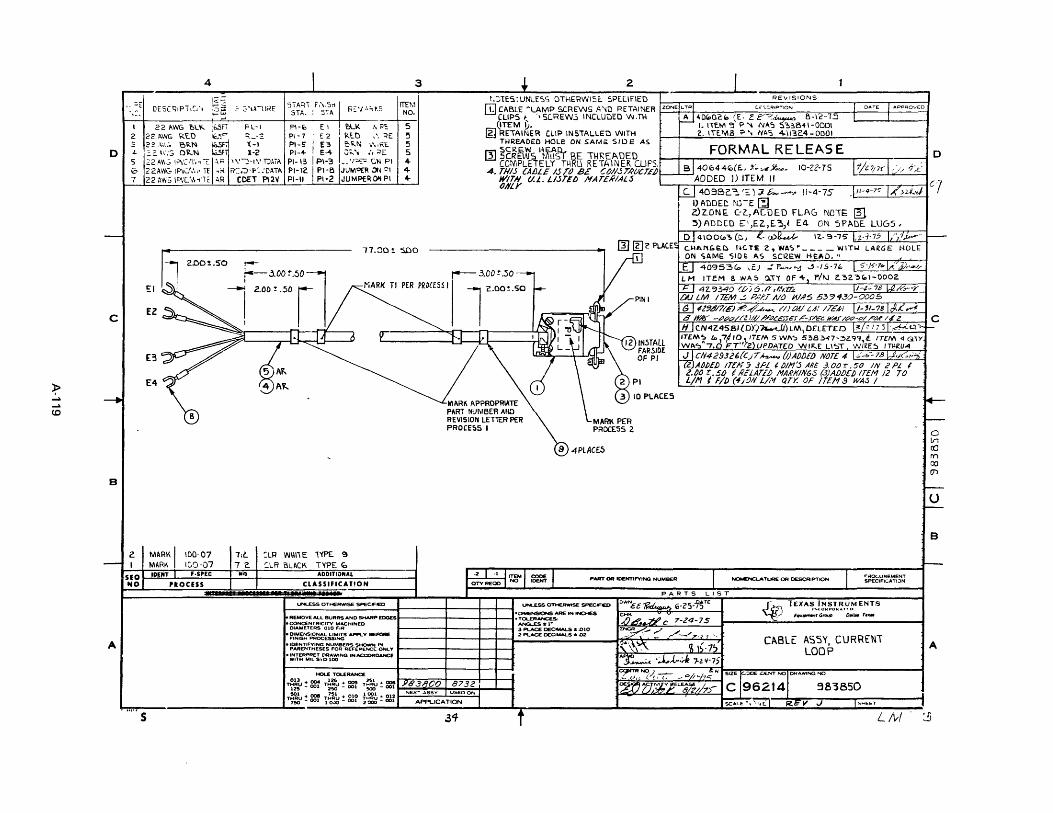
~ --c.o
,. -tl I
2 -
0 4
5 to 7
-
c
--+
B
4
22 AWG ~L'" :,;.sr. 22 ,,"WG REt) ~.~<"'
~~'~~'.~:; ~~ ~ 22 A'I.::; I ?V.: !\'.~ ~ I;;:; 22AWG- IP'JU:, ~ Tf ,;;\ 22 Po'll" IPVC.\hTE. "R
JJ EZ
£3
E4
8
FL-I
'(-I 1-2
f?::'.~.f': : [)ATA
con P\2'V
I
PI-~ Ell R.K A, ~ PI-7 . £2 RlD ,\ ~E PI-S' E~ I i:)RN ",RE PI-+ E~ J;:"', ;,;:(E PI-13 P\-3 ~_ 'l=--:'-= c.}l PI PI-\Z PI-B iJVMCfR ~l PI PHI PI -2 IJUMPE~ ~ PI
3
iTE"1 NO.
5 ~ !5 5 4-4-4-
2
!.:',lE5:UNlE:'S OTHERWI5~ SPECIFIED REviSIONS
[Q CABLE ~ LA MP SCREWS A" 0 RETAINER f-oZ_O_NE-+-L T:-"-t-:-I-::-:-..,...",._-:-=:---::_c::-" "o=::=-"'_PT_,o:,,"'':'-'-:--:-:::-==-_I-I=-DA_T.:..E _+-IA_PP_"..,:O __ V=-ED-j CLIPS f -, SC.REW.5 INCLUDED W.TH I A 14D"02'" (E, Z. E:''?~ B-\"2-1.5 1 1 QTEM 0. ~ I. HEM ~' P .... N!I'"J :S:'?B4 \ -000\
@] REiAINER CLIP IN51'ALLED WITH 2. \IE.MB ? .... ((AS 4-iI3~4-0DOI
o TI-IREAD£O HOLE: ON SAMii SlOE AS
III 5~~f~s 11~~ BE iH"EADED FORMAL RE LEAS E CCMPLETELY TI4RIJ RETI\INER CUPS. ~ - - I ~J T ' 4. THIS {AfJLE ISTtJ 8£ C~I/.5T/?/JCTE~ B 406441Q(~, ~v:,,,,>,oX.<>_ 10-22-75 'iZI/7f' "1/ tT/,-WITH (/./.. LlJT£/) I1AT£/?IALS I-- ADDED J) ITEM " ONLY L-.-r--r---~--~------,~--~-,,-~--IC '7
~409Bc.~f=:)J!£-_ ... 11-4-75 '\11-9- 7':' I,.(.ui'<-.j { I)AnDE~ NrE ~ z)Z.DN~ C-z..,ACDED FLAG NO\~ @]. !»ADD[D E')EZ.)E.~i E4 ON SPADE. LUGS,
-U I--B
Z. MrtRK lIDO. 07 11t. :LR Willi E 1'1PE. 9
---~I~~M~A~RK~~I~G~Q~·O~7~~~7~~~-=r~LR~B~L~A~CK~~T~~~P~E~~~ _________ ~ SEO~I~DE~N~T_~I~F~.S~PE~C~~ __ .~0-1 __________ ~A=DD~I~TI~O~NA~L~ ________ ~ r--T--~-r--~------------------------~------------------------------~I--I -2 I ·1 I ~ I COOE I PART OR IIl£HTIFY'NG NUMBER I NCIOoIENCl..ATUOE OR OESCR'PTION J
A
.. 0 'ROCESS CLASSIFICAT!ON I QTV REQO J J IDENT
. ,,,., S
r UNLESS OTt-tERWtSE SPECFED UNL.£SS ~SE 5P£CFlED
REMOVEALLBURRSA.--..DSHARP£0GE5I-____ --+ __ -I_-l--I:~AAElNtNCHES • CONCENTRICITY MACHINED ANGL.ES. 1-
DIAMETERS 010 FIR 3 Pl.ACE DECUALS • .010 • DIMENSIONAL LIMITS APPl. Y IIEFOAE 2 PLACE OCCIMALS • ~
FINISH PROCESSING
·W&E~~~~~':~~E~F~I~y I------+---I---l--I • :1~~A:~LE~·.~t~ING INACCOROAHCE 1------+-----4--+-1
HOL£ TOL£AANC£
T~:f!~ T~!~ T~:= pe3~CO 8732
Tr~ ~ ~ 1~: 8Jf 1~ ~ &If NEX~=~AT~:D ON
f
PARTS LIST
DWNee~ 6-cs-7'~TE
C;;~~ CV
7-24-7S
:,'~"':\ ~ 1~·7;' A~~ 'J.."(".;k H4-75
"rfO(.URE"MENT SPECIFICA TI.JN
r.w lEXAS INSTRUMENTS I-'CONPOHA"O
...; Eou.",.", Group (JMw , •••
CABLE ASSY. CURRtNI LOOP
L /'vI
A

LIST OF MATERIALS
Assembly Part No. Rev.
CABLE ASSY. CURRENT LOOP 1/F 0983850-0001
Item Quantity No.
TI Part No. Description Remarks
0001 00001.000 EA 0539903-0005 HOOD,CONN 15 PIN wiTH kETAINERS
0002 00001.000 E:A 0539409-0004 CONNECTOR,RCPT 15 PINS
0002A PI
0003 00010.000 EA 0539430-0004 CONTACT,SnCKE:T 24-20AWG .068 INSUL OIA
0004 00000.500 FT 0538347-3999 wiRE HOOKUP B-22 AWG 19 STR WHITE
0005 00006.500 FT 0972444-0011 CASLE,4 eONO 22 GA .195 00
0008 00004.000 EA 0972561-0002 TE:R~INAL,SLOT TONGUE *4 STUD(TAPE MTG)
0009 00004.000 EA 0418201-0060 STRAP,MARKER,ADJUSTABLE,PLASTIC
0011 REF EA 0910613-9901 CM~I TEST PRCGRA~ FOR CABLE ASSY,CURRENT
0012 00001.000 [A 0962511-0005 PLATE, 10, tOP CABLE
A-120

4
V.,RE OE5CR~PTlON
TOTAL 1';0 LENGTH
I c2,lAG eLK (CFtS III. 2- 1 RED .l J ORN T
0 4 YEL I , '5 1 BRN16FT5/N 6 =:: AIi~ WI1lTE I 3/N
-
c
B
2 MARl< I 100-07 712
- I foiMRK 100 -07 712
110 IIKJIT I F·I'EC 110
NO noells -A
I 3 2 I--_~~_~ _____ -_' ______ ~ Sl("~-_~E
START :,Pj,5t1 5TA. S1A
PG:-to PI-9 P2-1 l"~7D PH~ ~c-a
P':\-D PI-Ie 0'2-3 ~~o PI-I ;>2-1 CTR PHS :>2-20
LDET'Pi2V PHI PI-IO
CLR WHITE TlPE ~
REMARII5 .1El.! NO
NOTES. UNLESS OTHERWISE 5Pt.clf1E~ OJ CABLE (LAMP SC!=\E.WS "'NO RETI\\NER
CLIPS AND -,t:.REW5 INGLUDED W,TH QTEM 0.
~CABlE CLAMP SC.REWS AND RETAINt.R cLirs AND SCREWS INCLUDED WI1H~rrM -':"
3. RETAlr-.ER CLIP 1~5TALlEO WI1H n\~E"'DE.L 1-10LE. ON SAME SIDE AS SCReW HEAD_
~(ABLE C.lAlVIP DETAIL If'\ P2 SAME A~ PI.
151 SCREWS MUS" BE TIlREAOED C.OtJIPL8ElJ ~ THRU RE,AINER CLIPS. ~. TJ.JIS CABLE: IS TO 8t. CONsnWCTEO WITH
II L. Ll5 TED M"TERd4S t7Nt Yo
A 40(;446 :E) lo':,o •• Y..~ Sou U,7 .... AQDED I) ITEM 10
B 4-098Z4 (U~~....-.,.. 11'4-75 !)ADDE.D ND1E[§]
Z)ZONE. 4B i l.G~ FLA(' NCTED~, ~4\OO('1(O) ~ 1.,..).J/.-l- 1,-<#-15
C.HAN(;'ED NOTE '3. WAS"' ____ WITI-I ON "oAMb SIDE AS, SC~~w HEAD_"
~ 1-13103 lO 1 ~,--.' 7- 15-7" I) "EM ( Q"Y WAS ,
JJ 42.9340 (I:» C t..;\IJGI,,)~\S r;;1 LM ITEM
3 PIN W43 539430 - coos ~CN124585(O); ~(I) I71M4 PN WAS 4I1b34-2'OO, QTY IT[M'3 WAS 35 FT fZ) WIRE LIST, /THRUb D[~CR'P. WAS ZZ IIWG Ifile WilT, I THRlJ 5' I TEM NO'~ WERE B
..§.,JCIV'429-'77(-::) :/'~"'- (I)A{)O~O N-:JTE~ (2)AOOEO ITEV 7 3 ~<!. (' .oIM:5 .. n~?:t ';-0 IN 2 Pc ~ <'00 ~,.s-o (R;OlTE.o ~"'R,(;'/;I/<i.5 I~)
:J:!;f/kE:1 ::-:J i~f:-~':~b: f!J-~ 9W"$~~or.
DATE A("~PQOvED
1/Z-1/.,f' /~
1,_dol 'S td.-J 0
• z q 1!> If.il,bV' LAI<i::E HOLE
7/2I/7(.1....-J...
Of 1-5-78 rflR~ ~
'I-'/'~ f[}j.,v
-
B
CLR BLACI< TYPE £.
ADDITI?NAl r-~~~---r----~----------------------------~------------------------~------------~----L 2 1 I J ITEM' COQ£ I PART OA IDENTIFYING NU"'BER 'NOI.ENCLATURE OR OESCRtP-.t()fIII , CLASSIFICATION ...... I Q-ry HOD ! NO 'DENT
I UNLESS OT......::JNt1s.E SPEC/F'IED ~ESS OT.-.e:RWISE sPECIFIEO
- ()It.IIENS<)fIoIS ARE IN INCHES REMQvE ALL BuR'f$A .... O SHARPEDGESt-----;----t--t--I_ TOLERANCES C'()iI'.fCE~TRICITY IrIIIACHINEO ANGLES S 1-[)tAME TERS 010 F.R ) PLACE DECIMALS SOlO
f- r.::.~~s~~~~u. ... ~s APPLY BEFORE 2 PLACE CECIMALS ~ .02
•• !)(~TIFYING NuMBERS SHOWN .... PARENTHESES FOR REFEHE~CE ONLY t-----;----t--t--t
• :,~~R:~LE~Tr:~~ING IN ACCOROANCE t-----;----t--t--I
HOLE TOl.ERANCE
T7~~::::t T~~~ Tf!U:~ 5183800 a7?2
PARTS Lisr
DW"'c.E~ 8-12-o/!>TE
liZI ~~ 8-1"-75
CABLE ASSV/ 1l3A IKTERFt...."£
P,.fQCURE'AENT SFll£CIFt{..~Tt()N
A
~ .. ~""~.~ _____________________ y~. __ ~~_~~_I_: .• ~ __ 1_1_~~_~_: __ ~_?_~_1~_RU_I_:_~_f~_'~_~_T~_A_50_~_A_T_~ON_x_~_ON __ ~ ____ ~~ ________________ ~ ________________ ~~~~-_AL~£_r~"_'~~~~I~~~ __ E __ v ___ ~ ____ ~_>H_£~£T~~ ____ ~
5 3q .f LM

LIST OF MATERIALS
Assembly Part No. Rev.
CABLE ASSY. (113A) INTERFACE 0983854·0001 G
Item Quantity No.
TI Part No. DeSCription Remarks
0001 00001. 000 EA 0539903-0005 HUOO,CONN 15 PIN WITH PETAI~ER~
0002 00001.000 EA 0539409-0004 CONNECTu~,RCPT 15 PINS
0003 000C7.000 EA 0539430-0004 CONTACT,SOCKET 24-20AWG .068 INSUl OIA
0004 00006.500 fT 0972444-0012 CABLI::,5CONU,22 AWG,300 WV,PVC INSULATED
0005 00001.000 EA 0539409-0005 CONNECTOR,PLUG 2~ PINS
0006 00001. 000 EA 0539903-0001 HOCD,CONN 25 PIN wITH RETAINERS
0007 00005.000 EA 0418201-0060 STRAP,MARKER,AOJUSTABLE,PLASTIC
0008 00000.160 Ff 0538347-3999 wiRE HOOKUP B-22 AWG 19 STR WHITE
0009 00005.000 EA 0539430-0003 CO~TACT,PIN 24-20AWG .068 INSUL DIA
0010 REf EA 0970674-9901 OMNI TEST PROGRAM FOR CABLE ASSy,I~TFC
0011 00001.000 I:: A 0~62571-0005 PLATE, 10, EOP CABL!::
A-122

7 1'\
8
o '6
c
B
A
Ie. d 14- t..4A'hG .t'\l, hll, •• \1) ccAWG IPVI NI.(v.'Rl I", i'r;AWG 11-\'1. i"\'\llfti-~ £ ~ IT
f' \2\j/'r~ ,hl'-ltl
(nE~~Lll HLV DAIA 1"1111 Dr-1A.
""lGNU ~ARDLT
I'GNO dS D )~ Of \)H
11L-M i\;,)
B
" , 10
6 5 4 3
N,JTE..'-, dNl\ r.::.. UTrlt.t?WI_t.. ...:.Pt .. :,-I~k.u o ':'Ab~E l \. AMI' ,_KL'{~ ..... \\'h .. r t.- TAlll~\-' \ \. \\ _ "'NO Sl~H\~ \1\, .... 1 V W Iii lfl'" \
~ ~~t,b~'1'~I'~ ~jk~:::~(~'::tl~~'~~~::~;ULE - ON :.'\1'111:. '~IbE AS SCREW \\t:.A\')
2B It'~-~l ( __ A v\>-' vi "fAIL ,\10 h:: AI\U r~ ~lJ\M
[2] ~~~~~~DW~~I \~ ~~~ ~uw:~is :~\~~~~ I N ~ I
I~l ~~\~~JWk'1 T~\'~':lFT\~ H,[j ~;;E:.i\Of:l ':0M~t E'(\ Y
Qj '>li . .I;;V1Nb (ITEVt 13) FRLlM LONNELTDR PZ ,P3,
~~E ~~~XTI~~~S~ ~~~O 66~~ ~~: ~~~~MRU~I CONNEC.TOR.. ~ou~ING
2
ON LM! ITEM 14 piN 0
c
B
o

LIST OF MATERIALS
Assembly Part No. Rev. CABLE ASSY. EIA/AUX MODEM 0983855-0001 E
Item Quantity TI Part No. Description Remarks No.
0001 00001.000 EA 0539903-0005 HOOO.CONN 15 PIN WITH RETAINERS
0002 00001.000 EA 0539409-0001t CONNECTOR.RCPT 15 PINS
0002A PI
~O03 00002.000 EA 1l539903-0001 HOOO.CONN 25 PIN WITH RETAINERS
0004 00001.000 EA 0539409-0005 CONNE~TOR.PLUG 25 PINS
0004A P2
0005 00001.000 EA 0539409-0006 CONNECTOR, RCPT 25 PINS
0005A P3
00116 JOOO1.000 EA 1l539430-0006 CONTACT,PIN 24-20AWG .068 INSUL OU
0001 OOO~1.000 EA 0418201-0001 REPLACED BY 418201-0060
0008 Q0091.UIJO FT \01538347-2999 WIRE HOOKUP 8-24 AWG 19 STR WHITE
0009 00006.500 fT 0538347-3299 WIRE HOOKUP 8-22 AWG 19 STR RD/WH
0010 00006.500 FT 0538347-3099 .. IRE HOOKUP 8-22 AWG 19 STR BK/WH
0011 OOOl1.000 EA '0539430-0004 CONTACT, SOCKET 24-20AWG .068 INSUL DIA
U012 00000.250 FT 0411t34-3eOC 5LEEVE,PVC,3/8 DIA. BLACK
0013 J0019.500 FT 0411634-2600 SLEEVE,PVC .263 OrA .020 WAll
0014 ~HhJu2.000 EA 0972561-0002 TERMINAL,SLOTTED TONGUE NO.4 STUD
0015 REF EA 11970075-9901 TEST PROGRAM.CABLE ASSV EIA AUX MODEM
A-124

I I I I I I I I I I •
USER'S RESPONSE SHEET
Manual Title: Model 743/745 Data Terminal Maintenance Manual 984025-9702
Date of Manual:_7_-1_-7_8 __________ Date of this Letter: _______ _
User: _________________ Office/Dept. No.: ________ _
COmpany: _____________________________________ _
Street Address: ________________________________ _
City/State/Zip: _________________ . ____________ _
Please list any discrepancy found in this mafiua! by page, paragrapll, figure. or table number in the following space. If there 3re any other suqgp,slions that you wish to make, feel free to include them. Thank you.
Location in Manual Comment/Suggestion
NO POSTAGE NECESSARY IF MAILED IN U.S.A. FOLD ON TWO LINES (LOCATED ON REVERSE SrDE), STAPLE AND MAll

FOLD
BUSINESS REPLY MAIL No postage n~S5afY If mailed in me United States
Postage will be paid by
TEXAS INSTRUMENTS INCORPORATEO DIGITAL SYSTEMS DIVISION
P.O. BOX 1444 HOUSTON, TEXAS 77001
ATTENTION: TECHNICAL PUBLICATIONS MIS 670
FOLD
FIRST CLASS Permit No 6189 Houston • Texas

Sales and Service Offices of Texas Instruments are located throughout the United States and in major countries overseas. Contact the Digital Systems Division, Texas Instruments Incorporated, P.O. Box 1444, Houston,
4P Texas 77001, or call (713) 491-5115, for the location of the office nearest to you.
Texas Instruments reserves the right to chanle its product and service offerings at any time without notice.
TEXAS INSTRUMENTS INCORPORATED
Printed in U.S.A.


