58
CREATING SiO 2 SURFACE Silica surface - Materials Studio tutorial

CREATING SiO2 SURFACE
Silica surface - Materials Studio tutorial

Our goal – surface of SiO2

Import structure
• The XRD experiment gives us suchparameters as: lattice parameters, symmetry group and atom coordinates.
• To build the silica surface we can usethe unit cell of SiO2. Unit cell is the smallest repeatable part of the crystal.
• To open the structure select File |Import… | Structures | metal-oxides | SiO2_cristobalite_low and click Open.
SiO2 unit cell
4.978 Ǻ
6.9
48
Ǻ

Right click on the background of 3D atomistic view and select Display Style. Select Ball and stick and set values Stick radius = 0,1 and Ball radius = 0,4

Crystalography – Miller indices (hkl)
• Crystallographic planes are fictitious planes linking nodes in crystalstructure.
• They may be found in following way:
• ( 𝒉: 𝒌: 𝒍 ) = (𝑎
Δ𝑥:𝑏
Δ𝑦:
𝑐
Δ𝑧)
Y
𝑎
𝑏
(010)
(100)
Δ𝑥
(120)
(-110)
(010)
Δy

Cleave surface
• We cut the crystal along one of the crystallographic planes.
0 0 1 1 0 0 0 1 0
1 0 1 1 1 0 0 1 1
1 1 1 1 1 1 1 1 1

Miller Indices for Planes
1. Indentify the plane intercepts on the x, y and z axes.2. Specify intercepts in fractional coordinates.3. The the reciprocal of the fractional intercepts.

Miller Indices for Planes
The plane intersects x-axis at point a (1,∞,∞)

Miller Indices for Planes
Miller indices are the reciprocals of the parameters of each crystal face:
(1/1,1/∞,1/ ∞) (1 0 0)
(1/ ∞,1/ ∞,1/1) (0 0 1)
(1/ ∞, 1/1, 1/ ∞) (0 1 0)
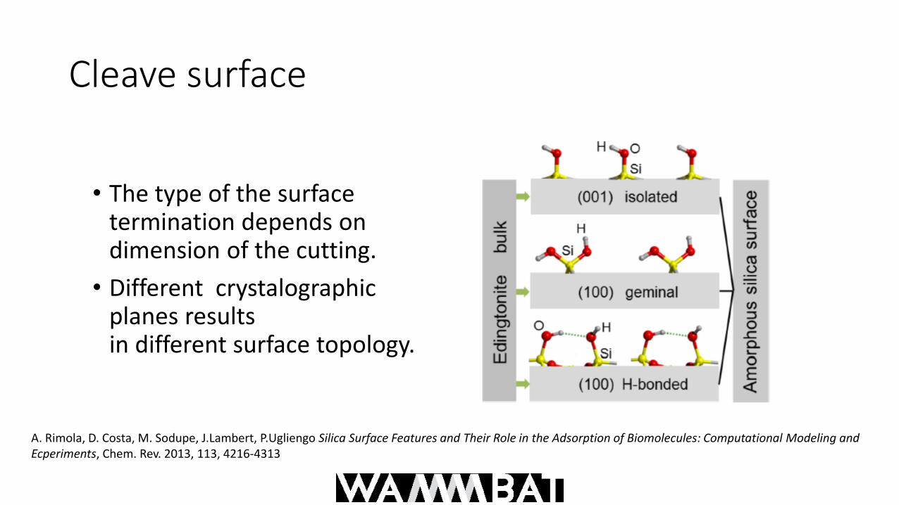
Cleave surface
• The type of the surfacetermination depends on dimension of the cutting.
• Different crystalographicplanes resultsin different surface topology.
A. Rimola, D. Costa, M. Sodupe, J.Lambert, P.Ugliengo Silica Surface Features and Their Role in the Adsorption of Biomolecules: Computational Modeling and Ecperiments, Chem. Rev. 2013, 113, 4216-4313

Cleave Surface dialog
• Select Build | Surfaces | Cleave Surface from the menu bar to open theCleave Surface dialog.
• Change Cleave plane (h k l): 0 0 -1 and Thickness to 1.75.
• Click the Cleave button and close the dialogwindow. (0 0 -1)
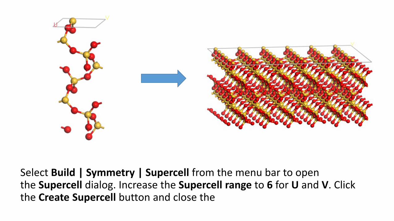
Select Build | Symmetry | Supercell from the menu bar to open the Supercell dialog. Increase the Supercell range to 6 for U and V. Click the Create Supercell button and close the dialog window.

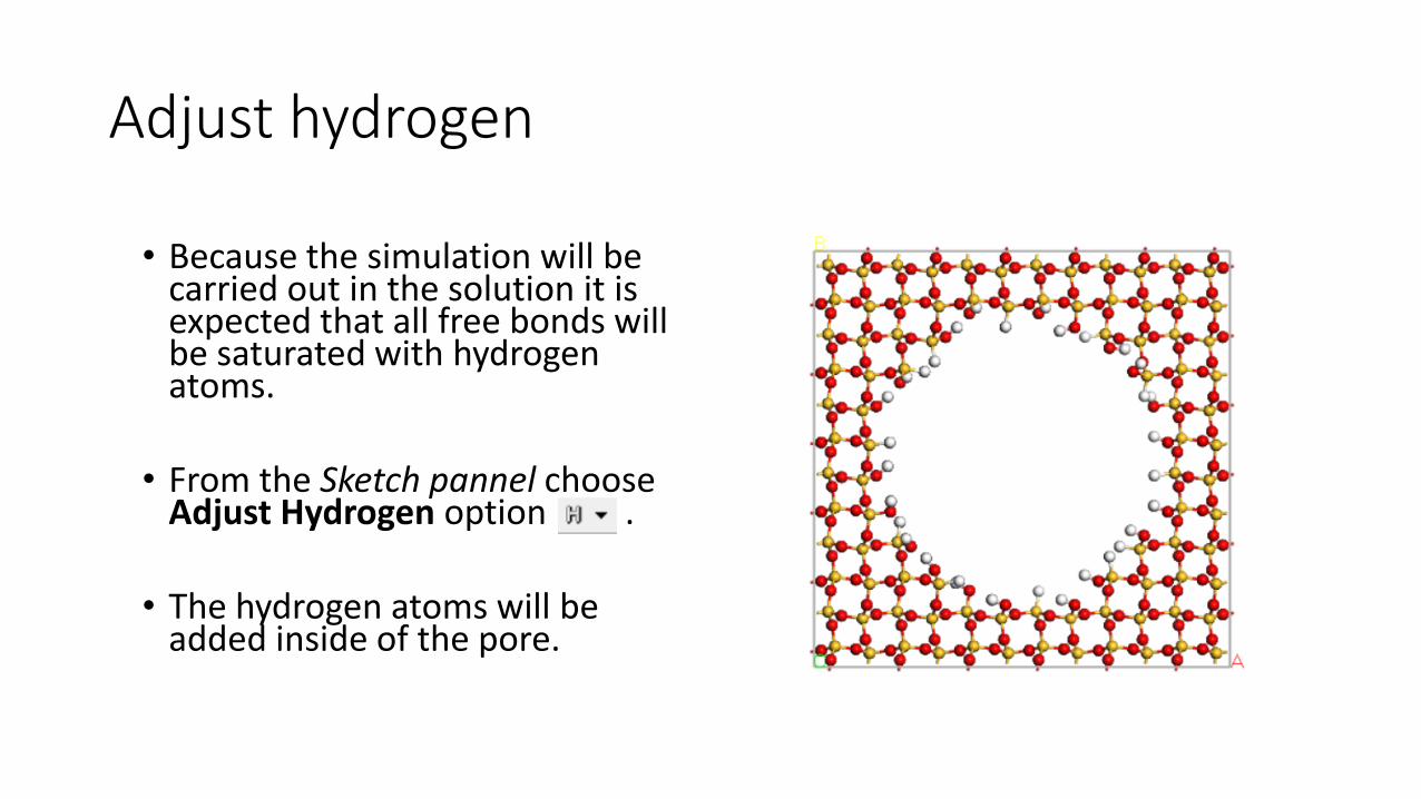
Adjust hydrogen
Because the simulation will be carried out in the solution it is expected that all free bondswill be saturated with hydrogen atoms.
From the Sketch pannel choose AdjustHydrogen option ..

Vacuum Slab
• Lets build the vacuum slab. Select Build | Crystals | BuildVacuum Slab…
• In Build Vacuum Slab Crystaldialog change the vacuumthickness from 10,00 Å to 25,00 Å and click Build.

Pore structure after multiplication of the surface system- Periodic Boundary Conditions.

Hydrophilic surfaceSilanol groups
Hydrophobic surfaceSilane groups

BUILDING SiO2 POROUS CRYSTAL
VMD tutorial

Our goal – porous structure of SiO2

Our goal – porous structure of SiO2

What is the PDB file?
• PDB file is the Protein DataBank format that provides astandard representation formacromolecular structure dataderived from X-ray diffractionand NMR studies.
• The structures which built inVMD programme are saved asPDB files with the propernames.

Inside the PDB file
Name of the crystal a b c in Angstroms α β γ in degrees Space group Z value
Number of atom Name of atom and residue Atom coordinates Element symbolOccupancy Beta

Building crystal – VMD Inorganic Builder
• First we have to build the bulk of SiO2.
• To do this select Extensions | Modeling| Inorganic Builder menu and choose the first option (Task builddevice).

Building crystal – VMD Inorganic Builder
In Inorganic Builder device select the propermaterial – Silicon Dioxide. In the next step inputthe following origin and box dimension to define basis vectors:
Box dimensions: 6 x 4.978 Ǻ6 x 4.978 Ǻ5 x 6.948Ǻ
Origin [Ǻ]
14.934 14.934 17.370
Box dimension
6 6 5
4.978 Ǻ
6.9
48
Ǻ

Building crystal – VMD Inorganic Builder
The values of the origin represents the center of the coordinate system. After input the Box dimensionsinto the dialog you can obtain the values StructureMin/Max.
Origin [Ǻ]
14.934 14.934 17.370
Box dimension
6 6 5

Why is it necessary?
Origin
14.934 14.934 17.370
In Materials Studio the origin coordinate are different compare with VMD. That’s why the StructureMin must be equal 0 everywhere.
MS
Origin
0 0 0VMD

Building crystal – VMD Inorganic Builder
• In Inorganic Builder device select the proper material – Silicon Dioxide. In the next step input the following origin and box dimensions to define basisvectors:
• On the VMD Display we can observe the changes of the crystal’s shape.
Origin
14.934 14.934 17.370
Box dimension
6 6 5

Add exclusion – pore shape
• To define shape of pore in SiO2 crystaluse Add exclusion option.
• In Add Block window we can define shapeand size of pore. To build our structure inputthe following parameters:
Click Add and Build device to addsilicon and oxygen atoms.
Block type Cylinder
Block name Silica pore
Bottom center X: 14.934 14.934 -2
Top center X: 14.934 14.934 36.74
Radius: 10
34.740 Ǻ
2 Ǻ
2 Ǻ

Our result
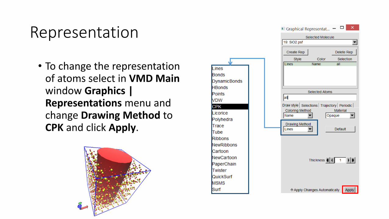
Representation
• To change the representationof atoms select in VMD Mainwindow Graphics | Representations menu and change Drawing Method to CPK and click Apply.

Our result

Add bonds function
• To add bonds to our structure we haveto select in Inorganic Builder windowTask | Add bonds.
• Afterwards select the second option to let VMD generate bonds in our structure.
• Next click on Select loaded moleculebutton and choose proper name of the structure. Click Select.
• In a Basis Vectors settings click on a Get Basis from PDB which let us to providethe proper values of basis vectors.
• Click Find Bonds.

Our result
To change the representation of atoms select in VMD Main window Graphics | Representations menu and change Drawing Method to CPK and click Apply.
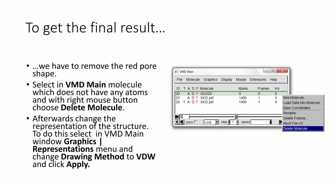
To get the final result…
• …we have to remove the red poreshape.
• Select in VMD Main moleculewhich does not have any atomsand with right mouse buttonchoose Delete Molecule.
• Afterwards change the representation of the structure. To do this select in VMD Mainwindow Graphics | Representations menu andchange Drawing Method to VDWand click Apply.

Final result

Save your structure• To save the structure built in VMD
select File | Save Coordinates… In Save Trajectory window in Selected atoms option choose alland click Save…
• Name your structure (e.gSiO2.pdb) and select All files (*.*) as a type of the file. Save yourstructure on the Desktop to havean easiest access to the file.

Import PDB file from VMD to MS• To import already built structure from
VMD to MS, open the Materials Studio programme and choose File | Import… and Open your SiO2.pdb file from the Desktop. For easiestsearching apply Protein Data Bank filtr near File name.
•
Folder with your SiO2.pdb file.

Display style
• To change the display style of the molecule right click on the background of 3D atomistic view. Choose the Display Style optionfrom the list.

Display Style
•
Select Ball and stick and set values Stick radius = 0,1 and Ball radius = 0,4.

Periodic Boundary Conditions
• Periodic Boundary Conditions (PBC) are often applied for approximating an infinite system. Instead of using infinite system we calculate small repeatable region called small simulation box. By usingPBC we can avoid the influence of the boundaries.

Periodic Boundary Conditions• To create a boundary conditions
in our system choose Build |Build Crystal change Entergroup to 1 p1 and click Build.

Our result
Adjust hydrogen
• Because the simulation will be carried out in the solution it isexpected that all free bonds willbe saturated with hydrogenatoms.
• From the Sketch pannel chooseAdjust Hydrogen option .
• The hydrogen atoms will be added inside of the pore.

To multiply your structure select Build | Symmetry | Supercell. In supercell dialog and inputthe following supercell range values: for A and B input 1 and for C: 2.

Delete 8 hydrogens one by one (that are bonded to the Si atom) from the rimof the pore and replace them with two carbon atoms bonded to each otherusing the Sketch tool.

To the carbon atoms add one nitrogen atom. Then click the Adjust hydrogenbutton and add one additional hydrogen to every nitrogen.
Rename file as SiO2_NH3_pore.

Porous SiO2 crystal with NH3 and COO-
• Open new 3D Atomistic file and from theprevious file (SiO2_NH3_pore) copy the
structure to the new file.

Rotate yourstructure 180°.
[If you have moreamino groupsformed at the back of the pore check ifthey are the illusioncaused by thePeriodic BoundaryCondition.]
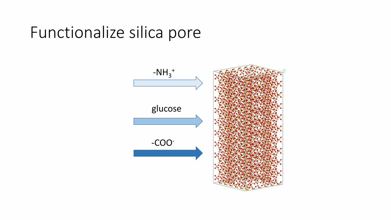
Functionalize silica pore
-NH3+
glucose
-COO-

Using the Sketch tool attach 3 carbon atoms to the oxygen atom placed inside the pore (but not too far from the rim).
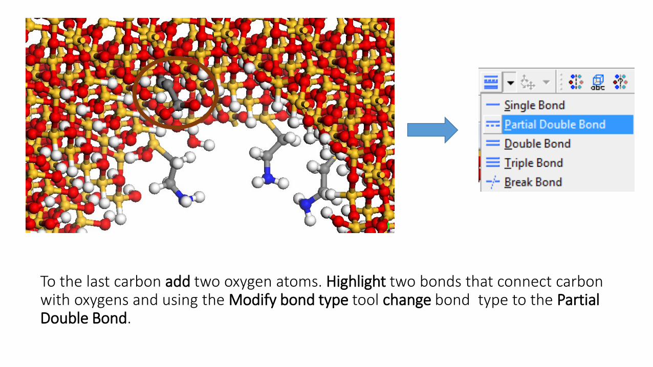
To the last carbon add two oxygen atoms. Highlight two bonds that connect carbonwith oxygens and using the Modify bond type tool change bond type to the PartialDouble Bond.

Repeat these steps 3 times to get 4 total COO- groups.Rename the file as poreSiO2_NH2COO.
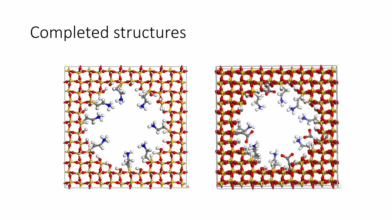
Completed structures

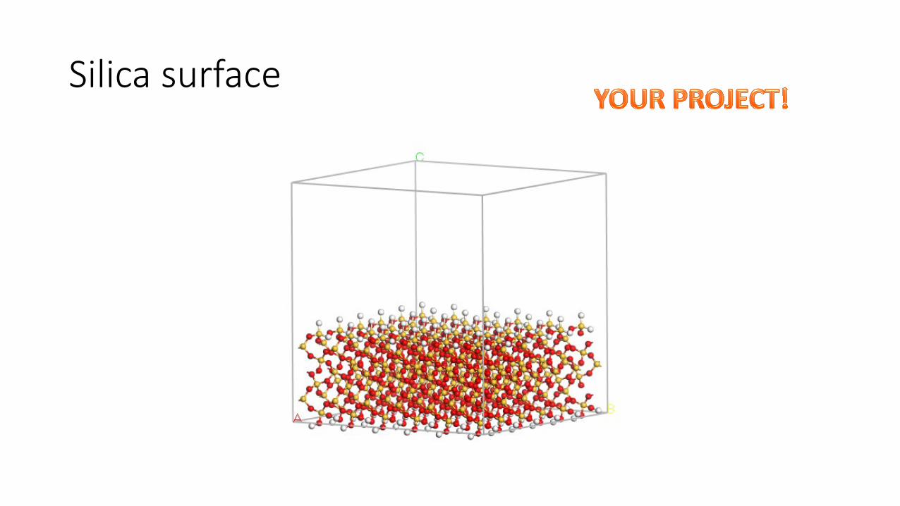
Silica surface
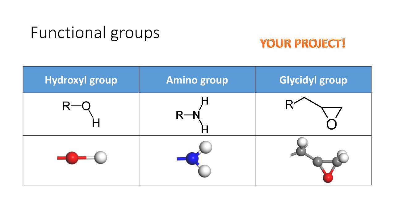
Functional groups
Hydroxyl group Amino group Glycidyl group

Functionalized silica
Example of functionalized silica surface – glycidyl group on hydrophobic side of silica pore.

Medicaments
Cisplatin Oxaliplatin Lidocaine
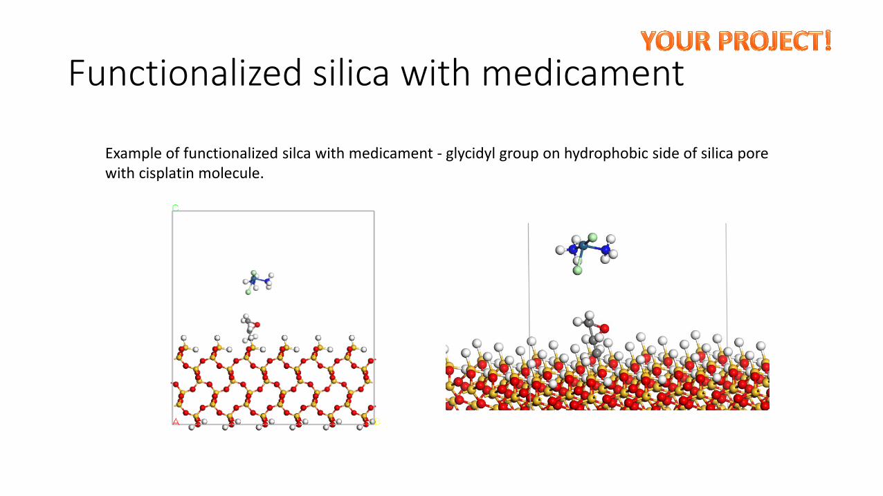
Functionalized silica with medicament
Example of functionalized silca with medicament - glycidyl group on hydrophobic side of silica porewith cisplatin molecule.


