www.infineon.com/sic SILICON CARBIDE 21 www.power-mag.com Issue 1 2014 Power Electronics Europe Practical Use of SiC Power Semiconductors Silicon Carbide (SiC) power devices are enabling components mainly in the context of higher switching frequencies and/or small footprints in power electronics. However, this trend imposes new challenges on the packaging of the chips. Typical stray elements like inductances become crucial elements in the circuit. In addition, different considerations regarding the thermal design in power modules arise when SiC chips are taken into consideration. Furthermore, the aspects of power density as well as the general utilization of SiC’s high temperature capability are important factors in reliable implementation of SiC-based power semiconductors in modern systems. The article will give an insight into how these boundary conditions can be implemented in innovative solutions using SiC chips. Peter Friedrichs, Senior Director SiC, Infineon AG, Erlangen, Germany SiC power technology, predominantly in form of Schottky diodes, is meanwhile established in the market. High-power solutions using power-module technologies have recently become available. Usually, the aim of such components is to enable system benefits, for example by increasing the switching frequency or reducing losses. If this is successful, the high cost of SiC-based components can be compensated by reduced efforts for passive elements and/or cooling. While the discrete, unipolar SiC devices as single chips are more or less ready to achieve higher frequencies (>100 kHz in PFC units), this is still a challenge for power modules. Solutions in a power range with traditional modules have high stray inductances and thus the di/dt is increased if combined with an increase in the frequency. A plug and play between SiC and Silicon at chip level in existing modules could devaluate the theoretical SiC performance. It is necessary to improve high-current modules in order to get the full benefit of SiC in the frequency range above 20 kHz. Current and power density considerations for state-of-the-art SiC devices Whilst the reduction of parasitic elements in power modules using SiC chips is in line with the approach also used for future Silicon solutions, it might happen that different optimization criteria will apply for the thermal design. The reason for this is that the cost contribution of chips in a power module with SiC is different from one with Silicon. Thus, the best solution for a given frame size with respect to semiconductor area placed in the module could be different. Furthermore, it is expected that the die size of a SiC transistor at 1200 V, for example, comes down to one tenth or less of the area needed in the current Silicon-based IGBT technology, assuming the same total losses for both options. This will result in a huge increase in power and current density, and will require more efforts with respect to an effective heat removal and the connection of chips to terminals. SiC diodes Several new generations of SiC Schottky diodes have been introduced since the first launch in 2001, each leading to a further increase in power density. Since 2006, Infineon has been using a Merged- Pin-Schottky (MPS) structure [1] for 600/650 V diodes, mainly in order to offer a sufficient surge-current capability. Other devices on the market are designed as JBS (Junction Barrier Schottky) diodes; from a design point of view, the layout is similar, the difference being that the main purpose of a JBS is to shield the electric field in reverse mode from the Schottky interface in order to keep the leakage current low, while in an MPS the main purpose is to offer surge current. In these diodes, only a part of the active area is used for the current flow; the rest is passive, being in operation in the MPS for only a short period of time (pulse mode). This again represents a further local increase in the current density, as shown in Figure 1 using the basic principle of the MPS diode as an example. The shown values today are close to the highest current densities for silicon power parts, which are known from low voltage transistors (e.g. 25 V at around 1300 A/cm²).Taking into account the voltage drop at operating temperature (which can Figure 1: Current densities in recent generations of Infineon’s 650 V MPS diodes (3G and 5G devices)
Transcript
www.infineon.com/sic SILICON CARBIDE 21
www.power-mag.com Issue 1 2014 Power Electronics Europe
Practical Use of SiC PowerSemiconductorsSilicon Carbide (SiC) power devices are enabling components mainly in the context of higher switchingfrequencies and/or small footprints in power electronics. However, this trend imposes new challenges onthe packaging of the chips. Typical stray elements like inductances become crucial elements in the circuit. Inaddition, different considerations regarding the thermal design in power modules arise when SiC chips aretaken into consideration. Furthermore, the aspects of power density as well as the general utilization of SiC’shigh temperature capability are important factors in reliable implementation of SiC-based powersemiconductors in modern systems. The article will give an insight into how these boundary conditions canbe implemented in innovative solutions using SiC chips. Peter Friedrichs, Senior Director SiC, InfineonAG, Erlangen, Germany
SiC power technology, predominantly inform of Schottky diodes, is meanwhileestablished in the market. High-powersolutions using power-moduletechnologies have recently becomeavailable. Usually, the aim of suchcomponents is to enable system benefits,for example by increasing the switchingfrequency or reducing losses. If this issuccessful, the high cost of SiC-basedcomponents can be compensated byreduced efforts for passive elementsand/or cooling.
While the discrete, unipolar SiC devicesas single chips are more or less ready toachieve higher frequencies (>100 kHz inPFC units), this is still a challenge forpower modules. Solutions in a powerrange with traditional modules have highstray inductances and thus the di/dt isincreased if combined with an increase inthe frequency. A plug and play betweenSiC and Silicon at chip level in existingmodules could devaluate the theoreticalSiC performance. It is necessary toimprove high-current modules in order toget the full benefit of SiC in the frequencyrange above 20 kHz.
Current and power densityconsiderations for state-of-the-art SiCdevicesWhilst the reduction of parasitic elementsin power modules using SiC chips is in linewith the approach also used for futureSilicon solutions, it might happen thatdifferent optimization criteria will apply forthe thermal design. The reason for this isthat the cost contribution of chips in apower module with SiC is different fromone with Silicon. Thus, the best solution fora given frame size with respect tosemiconductor area placed in the module
could be different. Furthermore, it isexpected that the die size of a SiCtransistor at 1200 V, for example, comesdown to one tenth or less of the areaneeded in the current Silicon-based IGBTtechnology, assuming the same totallosses for both options. This will result in ahuge increase in power and currentdensity, and will require more efforts withrespect to an effective heat removal andthe connection of chips to terminals.
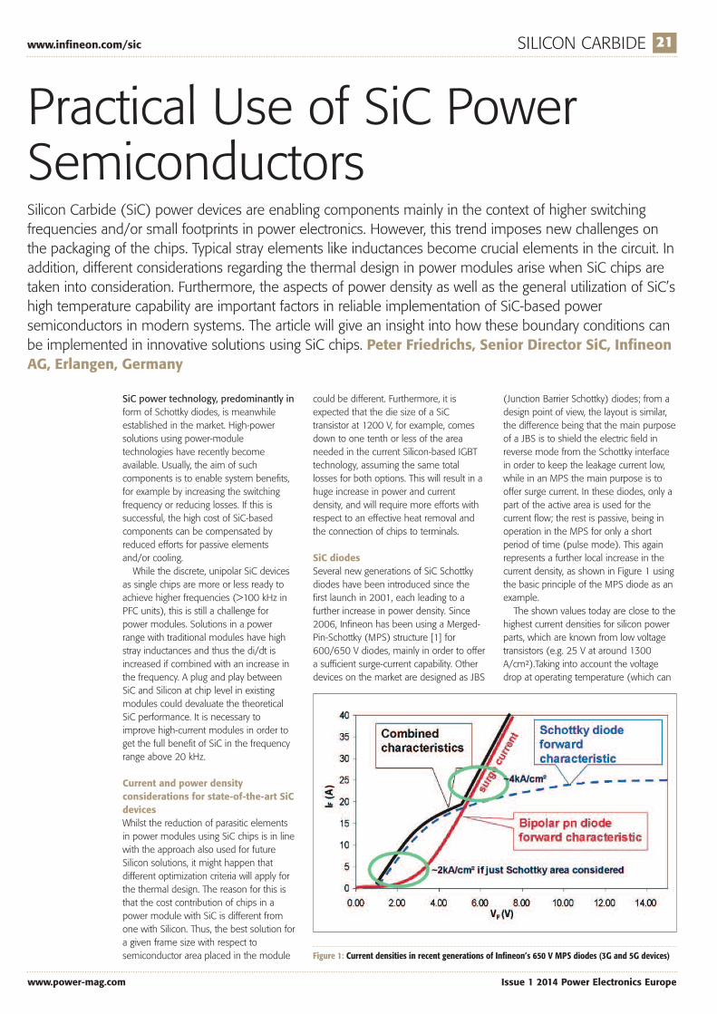
SiC diodesSeveral new generations of SiC Schottkydiodes have been introduced since thefirst launch in 2001, each leading to afurther increase in power density. Since2006, Infineon has been using a Merged-Pin-Schottky (MPS) structure [1] for600/650 V diodes, mainly in order to offera sufficient surge-current capability. Otherdevices on the market are designed as JBS
(Junction Barrier Schottky) diodes; from adesign point of view, the layout is similar,the difference being that the main purposeof a JBS is to shield the electric field inreverse mode from the Schottky interfacein order to keep the leakage current low,while in an MPS the main purpose is tooffer surge current. In these diodes, only apart of the active area is used for thecurrent flow; the rest is passive, being inoperation in the MPS for only a shortperiod of time (pulse mode). This againrepresents a further local increase in thecurrent density, as shown in Figure 1 usingthe basic principle of the MPS diode as anexample.
The shown values today are close to thehighest current densities for silicon powerparts, which are known from low voltagetransistors (e.g. 25 V at around 1300A/cm²).Taking into account the voltagedrop at operating temperature (which can
Figure 1: Current densities in recent generations of Infineon’s 650 V MPS diodes (3G and 5G devices)
22 SILICON CARBIDE www.infineon.com/sic
Issue 1 2014 Power Electronics Europe www.power-mag.com
be > 2V), it becomes obvious that heatgenerated by the power density at the chipwith >2kW/cm² can be effectivelyremoved only if effective heat spreading isimplemented between junction and case.
Another aspect of modern device designis the reduction of the die thickness. In thespecial case of vertical SiC devices, theactive layer is just a few µm thick, and thusany additional material below it is merelyan increase in the (differential) on-resistance and the thermal resistance ofthe chip [2]. It is thus reasonable to thinthe wafers down to the smallest possiblevalue, often defined by the handlingcapability in manufacturing. Infineonintroduced thin (110 µm) wafer deviceswith its 5th diode generation (5G), offeringa further step in power density, as shownin Figure 2.
But this benefit has a drawback – thethermal capacitance, which is importantunder pulse current stress, is also reduceddue to the shrunken volume of thesemiconductor. Technologies musttherefore be developed to compensate forthis, otherwise only reduced pulse ratingsare possible. One approach is a goodthermal connection of the chip to the leadframe, e.g. by solderless assemblytechnique, enabling the utilization of theunderlying copper as a support for pulsedoperation [3].
SiC transistorsThe focus today is on the implementationof unipolar high-voltage (600 V … 1700V) transistors, offering threshold-free linearI-V characteristics, integrated body diodes,and negligible dynamic losses comparedto the competing Si-IGBT technology. TheRon x A values expected for 600 Vcomponents that seem to be achievablelong term are around 1mΩcm² [4]. Thebenchmark with the above-mentionedlow-voltage Silicon technology shows that
such values are still a factor of 20 higherthan the best-in in-class devices for 25 Vtoday. So it seems that experience withSilicon is sufficient to handle high currentdensities for SiC transistors.
Nevertheless, one mode of operationwill need closer attention. It seems to bemandatory for the success of SiCtransistors in industrial applications tooperate the internal body diode as afreewheeling diode. There might be someconcerns regarding efficiency in thisoperation mode, because the forwardvoltage drop is too high; however, one canturn on the channel after a short deadtime and then the I-V characteristic inreverse mode is identical to or evenslightly better than in forward mode (seeFigure 3).
Anyway, there might be a critical
situation should the driver circuit fail whendiode mode is required by the system. Tocope with this mode, one may be forcedto define the actual current rating, not fromthe attractive threshold-less forward I-V, butout of the power handling capability inreverse mode. Thus, lowest VF is required,or alternative solutions for designing thediode function in the 3rd quadrant modemust be developed.
High-frequency optimizationReal power circuits with SiC chips insidecontain inductance and capacitance asmajor parasitic elements, and these causeserious deviations from perfect switching.Basic effects of parasitic inductance are: a voltage dip during turn-on of atransistor, caused by rise of current
a voltage spike during turn-off of atransistor, caused by current fall
the parasitic capacitance together withthe inductance form resonant circuits,which show damped oscillations aftereach switching transition
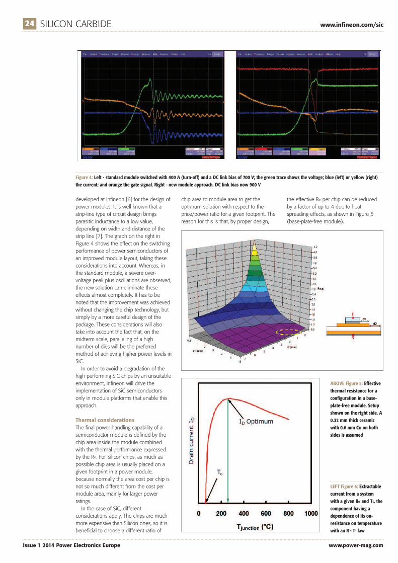
The effect of parasitics is already morepronounced when a combination of anIGBT with an SiC freewheeling diode isconsidered, since the diode performancealso speeds up the transistor and thus,under improper conditions, oscillationscould be observed as seen in Figure 4 (leftside) when no special precautions aretaken. Therefore, an optimum circuitdesign with minimum parasitic inductanceis a prerequisite for the optimization ofpower semiconductors towards lowestlosses [5].
To meet these demands, rules were
Figure 2: Chip thickness shrink effect on the maximum temperature of an SiC diode with 5.1mm2 areaon a copper lead frame and a power stress of 170 W; due to the smaller die thickness, the effective Rth
is reduced
Figure 3: SiCtransistors (exampleSiC JFET fromInfineon) in 3rdquadrant – channelmode possible toreduce losses byturning on thechannel infreewheelingoperation; however,in critical modes theI-V in diode modemight define thecurrent handlingcapability
24 SILICON CARBIDE www.infineon.com/sic
Issue 1 2014 Power Electronics Europe www.power-mag.com
developed at Infineon [6] for the design ofpower modules. It is well known that astrip-line type of circuit design bringsparasitic inductance to a low value,depending on width and distance of thestrip line [7]. The graph on the right inFigure 4 shows the effect on the switchingperformance of power semiconductors ofan improved module layout, taking theseconsiderations into account. Whereas, inthe standard module, a severe over-voltage peak plus oscillations are observed,the new solution can eliminate theseeffects almost completely. It has to benoted that the improvement was achievedwithout changing the chip technology, butsimply by a more careful design of thepackage. These considerations will alsotake into account the fact that, on themidterm scale, paralleling of a highnumber of dies will be the preferredmethod of achieving higher power levels inSiC.
In order to avoid a degradation of thehigh performing SiC chips by an unsuitableenvironment, Infineon will drive theimplementation of SiC semiconductorsonly in module platforms that enable thisapproach.
Thermal considerationsThe final power-handling capability of asemiconductor module is defined by thechip area inside the module combinedwith the thermal performance expressedby the Rth. For Silicon chips, as much aspossible chip area is usually placed on agiven footprint in a power module,because normally the area cost per chip isnot so much different from the cost permodule area, mainly for larger powerratings.
In the case of SiC, differentconsiderations apply. The chips are muchmore expensive than Silicon ones, so it isbeneficial to choose a different ratio of
chip area to module area to get theoptimum solution with respect to theprice/power ratio for a given footprint. Thereason for this is that, by proper design,
the effective Rth per chip can be reducedby a factor of up to 4 due to heatspreading effects, as shown in Figure 5(base-plate-free module).
Figure 4: Left - standard module switched with 400 A (turn-off) and a DC link bias of 700 V; the green trace shows the voltage; blue (left) or yellow (right)the current; and orange the gate signal. Right - new module approach, DC link bias now 900 V
ABOVE Figure 5: Effectivethermal resistance for aconfiguration in a base-plate-free module. Setupshown on the right side. A0.32 mm thick ceramicwith 0.6 mm Cu on bothsides is assumed
LEFT Figure 6: Extractablecurrent from a systemwith a given Rth and TC, thecomponent having adependence of its on-resistance on temperaturewith an R~T2 law
www.infineon.com/sic SILICON CARBIDE 25
www.power-mag.com Issue 1 2014 Power Electronics Europe
In addition, there is a trend towardshigher maximum chip temperatures, inorder to increase the removable heat for agiven die area, and thus its current-handling capability. It must be mentionedthat doing this will increase the absolutelosses, so that efficiency targets could beviolated, depending on the ratio of lossincrease to increase in power-handlingcapability. In contrast to IGBTs, this lossincrease might be huge for unipolar SiCdevices, because now a resistivecomponent with a heavy increase in theRon with temperature is in place, mostlywith a power law in the form of Ron ~ Tx,with x values between 2 and even 2.5, asrecently presented for high voltage SiCMOSFETs.
Taking this into account, one can seethat, for unipolar devices, a continuousincrease of Tj can even lead to a reductionin current-handling capability, becausemore power is dissipated than can beremoved by the increase of Tj. Figure 6shows this result for a typical dataset,assuming x=2 as the exponent in thepower law for the increase of theresistance with temperature.
In addition to these considerations, it isknown that the reliability of power systems,mainly the power cycling capability, is
degraded when the temperature swingbetween off state and maximumtemperature is increased [8]. Thus, for thesake of both efficiency and reliability, itmight be wiser to offer good cooling andkeep the temperature differences in thethermal stack low.
Literature[1] F. Dahlquist, J. Hancock, M. Treu,
R. Rupp, T. Reimann, “2nd Generation600 V SiC Schottky Diodes Use MergedPn/Schottky Structure For SurgeOverload Protection”, presented at APEC2006[2] R. Rupp, R. Gerlach, U. Kirchner, A.
Schlögl and R. Kern, „Performance of a650V SiC diode with reduced chipthickness”, Proceedings of ICSCRM2011, Mater. Sci. Forum, Vols. 717-720,pp. 921-924, 2012.[3] M. Holz, J. Hilsenbeck, R.
Otremba, A. Heinrich, P. Türkes, R.Rupp,„SiC Power Devices: ProductImprovement using DiffusionSoldering”, Mater. Sci. Forum, Vols. 615-617, pp. 613-616, 2009[4] Y.Tanaka, K.Yano, M.Okamoto,
A.Takatsuka, K.Fukuda, M.Kasuga,K.Arai, T.Yatsuo, “Fabrication of 700VSiC-SIT with Ultra-Low On-Resistance of
1.01mΩ•cm², Mater. Sci. Forum, Vols.257-529, pp. 1219-1222, 2006[5] Miller, Gerhard: New
Semiconductor Technologies ChallengePackage and System Setups, CIPS2010, Nuremberg. Germany[6] Bayerer et al: Power Circuit design
for clean switching, CIPS 2010,Nuremberg, Germany[7] Stockmeier, T, et.al: 1200 A, 3300
V IGBT Power Module exhibiting VeryLow Internal Stray Inductance, PCIM,Hong Kong, 1997[8] U.Scheuermann, R.Schmidt,
“Separating Failure Modes in PowerCycling Tests”, published at CIPS 2012,ISBN 978-3-8007-3414-6
To receive your owncopy of
subscribe today at: www.power-mag.com
Power Semiconductor Solutions Power Semiconductors