60
Silicon IP Cores Hardware acceleraon for seamless SoC integraon Product Catalog May 2019
Silicon IP Cores Hardware acceleration for seamless SoC integration
Product Catalog May 2019

2
Noesis Technologies P.C. Patras Science Park Stadiou Rd, Platani Rion GR-26504 - Patras GREECE Phone: +30 2610 911531 Email: [email protected]
www.noesis-tech.com
Rev. 1.5 Copyright © 2019, Noesis Technologies P.C. ALL RIGHTS RESERVED.

3
Disclaimer This document is written in good faith with the intend to assist the readers in the use of the product. Circuit diagrams and other information relating to Noesis Technologies products are included as a means of illustrating typical applications. Although the information has been checked and is believed to be accurate, no responsibility is assumed for inaccuracies. Information contains in this document is subject to continuous improvements and developments. Noesis Technologies products are not designed, intended, authorized or warranted for use in any life support or other application where product failure could cause or contribute to personal injury or severe property damage. Any and all such uses without prior written approval of Noesis Technologies will be fully at the risk of the customer. Noesis Technologies disclaims and excludes any and all warranties, including without limitation any and all implied warranties of merchantability, fitness for a particular purpose, title, and infringement and the like, and any and all warranties arising from any course or dealing or usage of trade. This document may not be copied, reproduced, or transmitted to others in any manner. Nor may any use of information in this document be made, except for the specific purposes for which it is transmitted to the recipient, without the prior written consent of Noesis Technologies. This specification is subject to change at anytime without notice. Noesis Technologies is not responsible for any errors contained herein. In no event shall Noesis Technologies be liable for any direct, indirect, incidental, special, punitive, or consequential damages; or for lost of data, profits, savings or revenues of any kind; regardless of the form of action, whether based on contract; tort; negligence of Noesis Technologies or others; strict liability; beach of warranty; or otherwise; whether or not any remedy of buyers is held to have failed of its essential purpose, and whether or not Noesis Technologies has been advised of the possibility of such damages. Copyright Notice No part of this specification may be reproduced in any form or means, without the prior written consent of Noesis Technologies.
Noesis Technologies P.C. Patras Science Park Stadiou Rd, Platani Rion GR-26504 - Patras GREECE Phone: +30 2610 911531 Email: [email protected]
www.noesis-tech.com
Rev. 1.5 Copyright © 2019, Noesis Technologies P.C. ALL RIGHTS RESERVED.
4
Index
About Noesis Technologies P.C. About Noesis Technologies P.C. About Noesis Technologies P.C. ………..…………4 Forward Error Correction Forward Error Correction Forward Error Correction ……..………………………5 Reed Solomon Codes …….………………………………6 ntRSE—Reed Solomon Encoder .………………..…7 ntRSD—Reed Solomon Decoder …….………….…8 Convolutional Codes …….……………………………….9 ntVIT—Viterbi Decoder ……………………………….10 Turbo Product Codes (TPC) ..……………………………..11 ntTPCE—Turbo Product Code Encoder .………12 ntTPCD—Turbo Product Code Decoder .…………..….13 ntCTCE—HomePlug AV2 CTC Encoder .………15 ntCTCD—HomePlug AV2 CTC Decoder .………..….16 Low Density Parity Check Codes (LDPC).………18 ntLDPCE-Ghn—G.hn LDPC Encoder ………………….19 ntLDPCD-Ghn—G.hn LDPC Decoder ….……………..….20 ntLDPCE-DVB-S2—DVB S2 LDPC Encoder ……………21 ntLDPCD-DVB-S2—DVB S2 LDPC Decoder .….……….22 ntLDPCE-DVB-S2X—DVB S2X LDPC Encoder ………24 ntLDPCD-DVB-S2X—DVB S2X LDPC Decoder …...….25 ntINT_DEINT—Interleaver/Deinterleaver…………....28 Voice & Data Compression Voice & Data Compression Voice & Data Compression ……..…………………29 ntG711—a/u law 64 kbps codec …….…………30 ntG726—ADPCM 16/24/32/40 kbps codec …31 ntG729—CS-ACELP 8 kbps codec …….…………32 ntCVSD—CVSD codec ………………..…….…………33 ntHUFF—Huffman compression engine ……34 Security Security Security …………..………………………..…………………35 ntAES8—AES Low Power Cipher …….…..36 ntAES32—AES High Speed Cipher …….…37 ntAES128—AES Ultra High Speed Cipher……….…….38 ntAES_XTS— XTS Mode Processor ………….…….39 ntRC4—RC4 Cipher …………………………………….40 ntSHA256—SHA 256-bit Hash Generator …...41
Telecom DSP Functions Telecom DSP Functions Telecom DSP Functions …………..………………..…42 ntFFT—FFT/IFFT Radix-2 Processor ……….…..43 ntCH_EST—OFDM Channel Estimator ………..44 ntSOD—Soft Output Demapper ……………..…..45 ntSYNC—Time & Frequency Synchronizer ……...46 ntAWGN—AWGN Channel Emulator …...……..47
Networking Networking Networking ……..……...………………………………….48 ntE1_G704—E1 Framer/Deframer ….…….…..49 ntT1_G704—T1 Framer/Deframer ….…….…..50 ntE3_E3—E2 & E3 Framer/Deframer ….….…..51 ntHDLC—High Level Data Link Controller …..52
Baseband PHYs Baseband PHYs Baseband PHYs …………..…...………………………….53 ntOFDM_BBP—OFDM Baseband Processor………...54 ntGhn_BBP—Home PLC Baseband Processor………56 ntG3_BBP—Smart Grid PLC Baseband Processor .. 57
IP CustomizationIP CustomizationIP Customization---System DesignSystem DesignSystem Design---Consulting Consulting Consulting …59

5
Noesis Technologies P.C. is a world wide leading silicon IP cores provider specialized in hard-ware implementation of high computational complexity telecom algorithms. Our hardware ac-celerator IP solutions allow telecom system developers to significantly off load demanding tasks from the CPU and to drastically decrease execution time thus boosting the overall system per-formance. Our IP cores present an industry leading combination of high performance, low pow-er and low die-area, as well as easy customization for adaptability to a wide range of applica-tions. Noesis offers a complete portfolio of Forward Error Correction IP core solutions that in-cludes Reed Solomon Codecs, Viterbi Decoders, Turbo Product and Turbo Convolutional Co-decs, LDCP Codecs, BCH codecs, (De)Interleavers, Channel Emulators. The company additionally offers a range of cores in the areas of security, networking, audio/voice/data compression, tele-com DSP including a complete OFDM baseband processor. Our company is also active in the development of integrated telecommunication systems that can used in education as well as in Research and Development applications. In the framework of this activity we have developed ComLab which is practically a cost efficient highly integrated development environment (IDE) that enables a system designer to rapidly build, configure and evaluate in real-time the performance of complex telecommunication systems. It is comprised of a Xilinx FPGA based board for the real-time HW emulation, a sophisticated application SW with interactive GUI capabilities for configuration, control and monitoring purposes as well as a rich portfolio of highly optimized telecom subsystem silicon IPs. ComLab platform is ideal for proof-of-concept rapid prototyping as well as an intuitive educational tool for engineers. Noesis Technologies also provides integrated solutions for WSN applications as well as develops disruptive technologies for the IoT market. In this framework, Noesis Technologies provides algorithms optimization and their effective implementation in FPGA technology using low power design techniques as well as embedded SW development for WSN nodes and application SW for base stations. Noesis Technologies is a Xilinx Alliance Member and an official IP Core Designer for Turbo Cod-ing technology. Its customer list includes U.S.A, Europe, Canada, Taiwan, China and India based companies active in telecom, defense and aerospace sectors. For further information please visit our web site www.noesis-tech.com
About Noesis Technologies P.C.
6
Error detection and correction codes are used nowadays in almost any digital transmission and storage system to ensure reliable transfer of information. Noesis Technologies offers a complete portfolio of forward error correction IP cores including Reed-Solomon, Viterbi, BCH, LDPC and Turbo Product codecs. These state-of-the-art hardware implementations have established Noesis Technologies as a worldwide leading provider in FEC IP core solutions. Noesis Technologies forward error correction IPs are developed to boost performance in wireless LANs and Internet, satellite communications, wireless broadband systems, optical networking, wireline access networks, data storage as well as in a variety of other target applications that require error detection and correc-tion techniques. Noesis FEC solutions are highly configurable, with optimized architectures that can be targeted to multiple wireless or wired standards and can meet the most demanding area and speed application requirements. All of the FEC IP cores are silicon proven (FPGA or ASIC) and technology independent for easy and risk-free porting to any target silicon process.
Forward Error Correction

7
Reed Solomon Codes
One of the most powerful and widespread used algebraic error cor-rection block code is Reed Solomon algorithm. It belongs to the family of maximum distance separable non-binary linear cyclic codes and it is exceptionally powerful when channels errors occurs in bursts. It is also good at correcting random errors. Noesis Technologies Reed Solomon highly parameterized hardware IP core solution can be used in any application that requires an RS based error correction control system. Its outstanding parameterization capability includes features such as configurable number of bits per symbol, maximum codeword length and maximum number of parity symbols. It also supports varying on the fly shortened and punctured codes. As a result of this parameterization and programmability feature any desirable code-rate can be easily achieved rendering the codec ideal for fully adaptive FEC applications. Erasures decoding for doubling the error correction capability as well as extended RS codes, burst or continuous decoding are also supported. The Noesis Technologies ntRS core has been specifically designed with fine-grain granularity in order to allow data path slices reconfigurability. The end-user can configure the number of slices in the data-path array in order to achieve the optimum ratio of throughput-rate vs silicon area and thus resulting into highly efficient hardware implementations.
Features
Fully configurable, time-domain, high throughput, Reed Solomon De-coder.
Supports different Reed Solomon coding standards.
Variable on the fly code rate adaptation by varying codeword length and/or number of parity symbols.
Variable bits per symbol, odd or even number of parity symbols.
Variable codeword length on a codeword by codeword basis.
Variable number of errors corrected on a codeword by codeword basis.
Supports shortened, punctured and extended codes.
Parameterized architecture allows optimum ratio of throughput-rate vs silicon area.
User configured primitive polynomial.
User configured generator polynomial.
Single or multiple symbol rate clock.
Continuous decoding with no gaps between codewords.
Predictable latency.
Counts number of errors and flags uncorrectable codewords.
Fully synchronous design, using single clock.
Silicon proven in ASIC and FPGA technologies for a variety of applica-tions.
Forward Error CorrectionForward Error Correction

8
ntRSE Fully Configurable Reed Solomon Encoder
The ntRSE core implements the Reed Solomon encoding algorithm and is parameterized in terms of bits per symbol, maximum codeword length and maximum number of parity symbols. It also supports varying on the fly shortened codes. Therefore any desirable code-rate can be easily achieved rendering the encoder ideal for fully adaptive FEC applications. The ntRSE core supports continuous or burst encoding. The implementation is very low latency, high speed with a simple interface for easy integration in SoC applications.
Silicon Vendor Device Resources Fmax (MHz) Configuration
Xilinx Virtex-2 585 CLB Slices 167 RS(255,239)
Altera Stratix-II 333 ALUTs 162 RS(255,239)
TSMC 0.18 μm RS(255,239) 2500 gates 250
The ntRSE core has been targeted to both ASIC and FPGA technologies for various applications. Noesis Technolo-gies can also deliver netlist versions of the core optimized to specific area resources and performance require-ments.
Forward Error CorrectionForward Error Correction
ntRSE
DIN
DVAL
CLK
RSTB
SRST
CDSYNC
NVAL
TVAL
DOUT
CDWINFO
Parity UnitCoefficient Unit
Control UnitCDWPAR

9
ntRSD Fully Configurable Reed Solomon Decoder
Forward Error CorrectionForward Error Correction
The ntRSD core implements a time-domain Reed-Solomon decoding algorithm. The core is parameterized in terms of bits per symbol, maximum codeword length and maximum number of parity symbols. It also supports varying on the fly shortened codes. Therefore any desirable code-rate can be easily achieved rendering the decoder ideal for fully adaptive FEC applications. The ntRSD core supports erasure decoding thus doubling its error correction capability. The core also supports continuous or burst decoding. The implementation is very low latency, high speed with a simple interface for easy integration in SoC applications.
Silicon Vendor Device Resources Fmax (MHz) Configuration
Xilinx Virtex-2 RS(255,239) 2765 CLB Slices / 3 Block RAMs 88
Xilinx Virtex-5 1490 CLB Slices / 3 Block RAMs 174 RS(255,239)
Xilinx Spartan-3 2810 CLB Slices / 3 Block RAMs 50 RS(255,239)
Altera Stratix-GX RS(255,239) 5865 LCs / 3 Block RAMs 83
TSMC 0.18 μm RS(255,239) 25 K gates / 12 K RAM bits 200
The ntRSD core has been targeted to both ASIC and FPGA technologies for various applications. Noesis Technologies can also deliver netlist versions of the core optimized to specific area resources and performance requirements.
CLK
RSTB
SRST
POLYNOMIALS(x) L(x) EL(x) EM(x)
CODEWORD MEMORY
DIN
DOUT
MAINCONTROL
ERRLOC
ERRMAG
ERRNUM
UNCORR
CDWSTRT
CDWEND
CDWNEW
CDWINFO
DVAL
CDSYNC
NVAL
PVAL
ERROR MAGNITUDES
MEMORY
ERROR LOCATIONS MEMORY
COEFFICIENTS MEMORY
GALOIS FIELDMEMORY
ERAS
SYNDROMES &ERASURES
POLYNOMIALCOMPUTATION
ERROR POLYNOMIAL COEFFICIENTS
COMPUTATION
ERROR LOCATIONS COMPUTATION
ERROR MAGNITUDES COMPUTATION
ERROR CORRECTION
ntRSD
10
Convolutional Codes
Linear convolutional codes are very well suited for random channel errors correction. When combined with Viterbi decoding algorithm can exploit the soft decision information provided by the demodulator and thus taking advantage of the 2dB coding again when compared with hard decision decoding. In application cases where noise is predominantly Gaussian then when the convolutional codes are concatenated with block codes result in an extremely powerful error correction control system.
Features
Fully configurable, high throughput convolutional FEC system based on Viterbi Decoder algorithm.
Supports different convolutional coding standards.
Parameterizable constraint length, code rate, generator coefficients and soft bits.
Parameterizable puncturing for full code rate control.
Programmable traceback depth.
Supports zero terminating and tail biting Viterbi decoding algorithm.
Soft or hard decision decoding.
Supports both continuous and burst input data flow.
Supports both block and continuous based decoding.
Fixed Viterbi decoder latency.
Single or multiple symbol rate clock.
Continuous decoding with no gaps between codewords.
Predictable decoder latency.
Area efficient design.
Fully synchronous design, using single clock.
Silicon proven in ASIC and FPGA technologies for a variety of applica-tions.
Forward Error CorrectionForward Error Correction

11
Forward Error CorrectionForward Error Correction
ntVIT Fully Configurable Viterbi Decoder
Convolutional FEC codes are very popular because of their powerful error correction capability and are especially suited for correcting random errors. The most effective decoding method for these codes is the soft decision Viterbi algorithm. ntVIT core is a high performance, fully configurable convolutional FEC core, comprised of a 1/N convolutional encoder, a variable code rate puncturer/depuncturer and a soft input Viterbi decoder. Depending on the application, the core can be configured for specific code parameters requirements. The highly configurable architecture makes it ideal for a wide range of applications. The convolutional encoder maps 1 input bit to N encoded bits, to generate a rate 1/N encoded bitstream. A puncturer can be optionally used to derive higher code rates from the 1/N mother code rate. On the encoder side, the puncturer deletes certain number of bits in the encoded data stream according to a user defined puncturing pattern which indicates the deleting bit positions. On the decoder side, the depuncturer inserts a-priori-known data at the positions and flags to the Viterbi decoder these bits positions as erasures. The Viterbi decoder uses a maximum-likelihood detection recursive process to correct errors in the data stream. The Viterbi input data stream can be composed of hard or soft bits. Soft decision achieves a 2 to 3dB increase in coding gain over hard-decision decoding. Data can be received continuously or with gaps.
Silicon Vendor Device Resources Fmax (MHz) Configuration
Xilinx Virtex-5 2200 CLB Slices / 4 Block RAMs 150 1/2 rate, constraint length 7
Altera Stratix-III 7384 ALUTs / 8 M144K Block RAMs 100 1/2 rate, constraint length 7
TSMC 180 nm 1/2 rate, constraint length 7 50K gates / 9K RAM bits 230
The ntVIT core has been targeted to both ASIC and FPGA technologies for various applications. Noesis Technologies can also deliver netlist versions of the core optimized to specific area resources and performance requirements.
ntVIT
DATA_IN
TB_DEPTH
CLK
RSTB
SRST
BLKSTRT_I
DRS
BLKEND_I
DVAL
BLKSTR_OMain
Control
Unit BLKEND_O
Add Compare
Select Unit
ERASE
DEC_DATA
Survivor Metric
UnitBranch Metric UnitDepuncturer UnitPUNC_VECT
MOD
1/n code rate Viterbi decoding engine
k/n code rate decoding engine
ntCONV
DATA_IN
CLK
RSTB
SRST
BLKSTRT_I
DRS
BLKEND_I
DVALConvolutional
Encoder
Unit
MOD
ENC_DATA
Puncturer Unit
PUNC_VECTBLKSYNC
1/n code rate encoding engine
k/n code rate encoding engine

12
Turbo Product Codes
Turbo Product Codes (TPCs) exhibit excellent performance in mod-erate to high signal to noise ratios. Since TPCs have more advantage when a high rate code is used, they are ideal for commercial applications in wireless and satellite communications. Noesis Technologies ntTPC Turbo Product Codec solution is consist-ed of the Turbo Product Encoder (ntTPCE) and the Turbo Product Decoder (ntTPCD) IP cores. The ntTPC cores can be used in a variety of applications, including, wireless broadband communications, optical transmission systems, free space optical communication,
satellite modems. The product code C is derived from two/three constituent codes, namely C1, C2 and optionally C3, thus supporting 2D or 3D codes. The information data is encoded in two/three dimensions. Every row of C is a code of C2 and every column of C is a code of C1. When the third coding dimension is enabled, then there are C3 C1*C2 data planes. The ntTPC cores support both e-Hamming and Single Parity codes as the constituent codes. The cores also support shortening of rows or columns of the product table, as well as turbo shortening. Shortening is a way of providing more powerful codes by removing information bits from the code. The construction of a two dimensional (NC-SHT_C, KC-SHT_C) × (NR-SHT_R, KR-SHT_R) code derived from the original (NC, KC) × (NR, KR) code is shown in the figure.
Column Parity Bits
Row
Parity
Bits
Information Bits
SHT_TURBO
1
SHT_R
SHT_C
0
0
KR-1 NR-1
KC-1
NC-1
Features
Encoder and decoder, support extended Hamming (256,247), (128,120), (64,57), (32,26), (16,11), (8,4) and Single Parity (256,255), (128,127), (64,63), (32,31), (16,15), (8,7) constituent error correcting codes.
3D encoding/decoding support with Single Parity (4,3) constituent code.
Highly programmable and parameterizable cores in terms of error correction capability, code rate, decoding iterations, decoding test patterns and scalability of design architecture.
Minimum system resources utilization and maximum resources reuse with one Single TPC elementary decoder instance for low power applica-tions, producing up to 10Mbps information throughput (100Mhz – 4 decoding iterations).
Small area footprint of the elementary decoder also allows an alterna-tive high throughput design approach with a number of cascaded / parallelized elementary decoders (plus the extra memories overhead), in order to reduce internal data re-iterations.
Flexible generic architecture with various combinations of parallelism options providing any desired application trade-off between area, per-formance and throughput rates.
Decoding algorithm achieves competitive performance results with the minimum possible test patterns and decoding iterations.
Bit serial encoder input/output interface. Soft input – soft output (SISO) serial decoder interface.
Flexible and programmable code rates, ranging from 0.1875 to 0.9922 (without shortening).
Additional programmability support for shortening of any selected code rate.
Programmable number of algorithmic iterations.
Simple yet robust encoder and decoder cores interface for optimum data flow control.
Synchronous single clock design.
Silicon proven in ASIC and Xilinx FPGA implementation technologies.
Forward Error CorrectionForward Error Correction

13
ntTPCE Configurable Turbo Product Code Encoder
The ntTPCE core receives the information bits row by row from left to right and transmits the encoded bits in the same order. It consists of a row, column and 3D encoder. The row encoder encodes the data row-wise (C2). The encoded data produced from the row encoder are stored in an intermediate memory and reordered in a column-wise fashion. Once a full column has been written in the memory, the data are encoded column-wise by the col-umn encoder (C1). When 3d encoding is employed, the encoded data produced from the column encoder are stored in an intermediate memory and reordered in a 3d-plane-wise fashion. The C3 data planes are encoded by an SPC(4,3) encoder (C3). Before output encoded information data are being reordered in row-wise fashion.
Silicon Vendor Device Resources Fmax (MHz) Configuration
Xilinx Kintex 7
XC7K410T-2 334 Slices / 9216 Memory Bits 224 64 bits/word—2D
Xilinx Kintex 7
XC7K410T-2 439 CLB Slices / 215040 Memory Bits 208 256 bits/word—3D
The ntTPCE core has been synthesized using Xilinx ISE Design Suite tools. The core has been targeted to Kintex-7 XC7K410T-2 FFG900 device with a default balanced optimization strategy between area and timing. The imple-mentation details for the configurable ntTPCE core, as shown in the table range from the 64 bits/word—2D en-coder to 256 bits/word—3D encoder configurations.
Forward Error CorrectionForward Error Correction
Row
Encoder
Wrapper
Row to
Column
Memory
Controller
Row to Zeta
Memory
Controller
Zeta
Encoder
Wrapper
Column
Encoder
Wrapper
Output
Memory
Controller
DOUT
DVAL
BLK_STRT
BLK_END
ntTPCE
Datapath
Controller
BLK_SYNC
SHT_C
SHT_R
SHT_TURBO
CODE_Z
CODE_C
CODE_R
DIN
DRS
CLK
RSTB
SRST

14
ntTPCD Configurable Turbo Product Code Decoder
The ntTPCD decoder receives soft information from the channel in the 2’s complement number system and the input samples are received row by row from left to right. The decoded soft information is output in the same or-der. The implemented decoding algorithm computes the extrinsic information for every dimension C1, C2, C3 by iteratively decoding words that are near the soft-input word. These words are called test patterns and their num-ber is pre-configurable. All C1, C2, C3 words decoding takes place in a main decoding unit, the programmable ele-mentary Soft Input Soft Output (SISO) decoder. An advanced scalable and parametric design approach produces custom design versions tailored to end customer applications design tradeoffs. The architecture of one elementary SISO decoder shown below is parameterizable in terms of maximum constitu-ent code size (64,128,256 bits), optional 3D codes support and maximum parallel test patterns processing (8,16,32) and soft bits.
Depending on system trade-offs / requirements, one or more SISO decoders may be used in one of the following schemes:
The following figures demonstrate kintex-7 device resources utilization for various con-figurations of the single SISO decoder archi-tecture.
The BER vs SNR performance of the ntTPCD for various code rates,
QPSK modulation, 8/16/32 test patterns and 2D/3D decoding are
demonstrated in the following curves:
Forward Error CorrectionForward Error Correction
15
ntCTCE HomePlug AV2 CTC Encoder
Forward Error CorrectionForward Error Correction
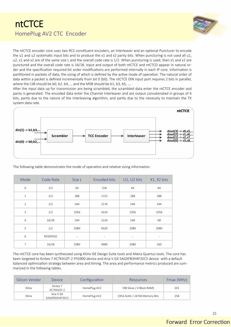
The ntCTCE encoder core uses two RCS constituent encoders, an Interleaver and an optional Puncturer to encode the u1 and u2 systematic input bits and to produce the x1 and x2 parity bits. When puncturing is not used all u1, u2, x1 and x2 are of the same size L and the overall code rate is 1/2. When puncturing is used, then x1 and x2 are punctured and the overall code rate is 16/18. Input and output of both ntCTCE and ntCTCD appear in natural or-der and the specification required bit order modifications are performed internally in each IP core. Information is partitioned in packets of data, the sizing of which is defined by the active mode of operation. The natural order of data within a packet is defined incrementally from bit 0 (b0). The ntCTCE DIN input port requires 2 bits in parallel, where the LSB should be b0, b2, b4, … and the MSB should be b1, b3, b5, …. After the input data up for transmission are being scrambled, the scrambled data enter the ntCTCE encoder and parity is generated. The encoded data enter the Channel Interleaver and are output concatenated in groups of 4 bits, partly due to the nature of the Interleaving algorithm, and partly due to the necessity to maintain the TX system data rate.
Silicon Vendor Device Resources Fmax (MHz) Configuration
Xilinx Kintex 7
XC7K410T-2 198 Slices / 4 Block RAMS 201 HomePlug AV2
Xilinx Aria V GX
5AGXFB3H4F35C5 1954 ALMs / 24704 Memory Bits 258 HomePlug AV2
The ntCTCE core has been synthesized using Xilinx ISE Design Suite tools and Altera Quartus tools. The core has been targeted to Kintex-7 XC7K410T-2 FFG900 device and Aria V GX 5AGXFB3H4F35C5 device with a default balanced optimization strategy between area and timing. The area and performance metrics produced are sum-marized in the following tables.
ntCTCE
Mode Code Rate Encoded bits U1, U2 bits Size L X1, X2 bits
0 1/2 256 64 64 64
1 1/2 1152 288 288 288
2 1/2 544 2176 544 544
3 1/2 1056 4224 1056 1056
4 16/18 544 1224 544 68
5 1/2 2080 8320 2080 2080
6 RESERVED - - - -
7 16/18 2080 4680 2080 260
The following table demonstrates the mode of operation and relative sizing information.
16
ntCTCD HomePlug AV2 CTC Decoder
Forward Error CorrectionForward Error Correction
ntCTCD
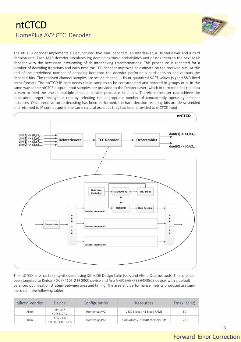
The ntCTCD decoder implements a Depuncturer, two MAP decoders, an Interleaver, a Deinterleaver and a hard decision unit. Each MAP decoder calculates log domain extrinsic probabilities and passes them to the next MAP decoder with the necessary interleaving of de-interleaving transformations. This procedure is repeated for a number of decoding iterations and each time the TCC decoder improves its estimate on the received bits. At the end of the predefined number of decoding iterations the decoder performs a hard decision and outputs the decoded bits. The received channel samples are scaled channel LLRs or quantized SOFT values (signed S8.3 fixed point format). The ntCTCD IP core needs these samples to be concatenated and ordered in groups of 4, in the same way as the ntCTCE output. Input samples are provided to the Deinterleaver, which in turn modifies the data stream to feed the one or multiple decoder parallel processor instances. Therefore the user can achieve the application target throughput rate by selecting the appropriate number of concurrently operating decoder instances. Once iterative turbo decoding has been performed, the hard decision resulting bits are de-scrambled and returned to IP core output in the same natural order, as they had been provided to ntCTCE input.
Silicon Vendor Device Resources Fmax (MHz) Configuration
Xilinx Kintex 7
XC7K410T-2 2330 Slices / 41 Block RAMS 80 HomePlug AV2
Xilinx Aria V GX
5AGXFB3H4F35C5 5708 ALMs / 798848 Memory Bits 72 HomePlug AV2
The ntCTCD core has been synthesized using Xilinx ISE Design Suite tools and Altera Quartus tools. The core has been targeted to Kintex-7 XC7K410T-2 FFG900 device and Aria V GX 5AGXFB3H4F35C5 device with a default balanced optimization strategy between area and timing. The area and performance metrics produced are sum-marized in the following tables.
17
ntCTCD HomePlug AV2 CTC Decoder
Forward Error CorrectionForward Error Correction
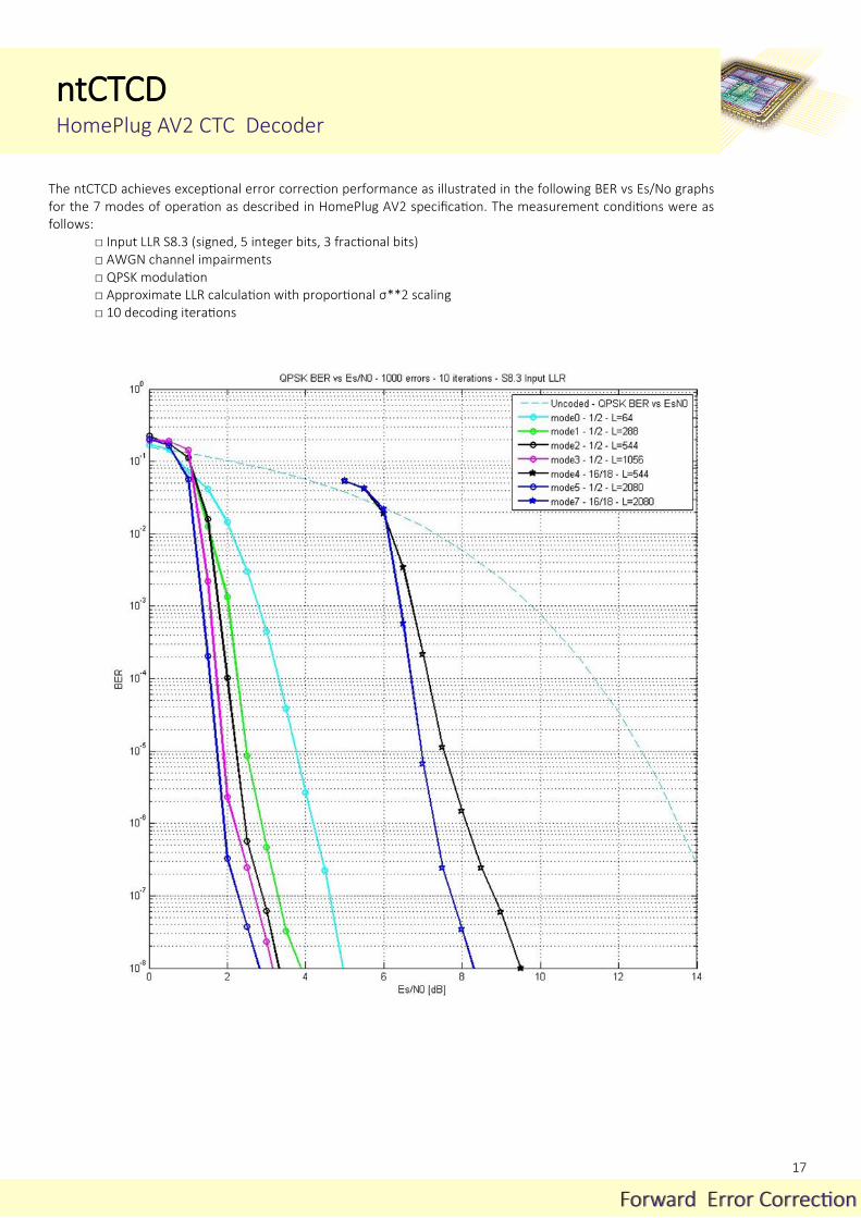
The ntCTCD achieves exceptional error correction performance as illustrated in the following BER vs Es/No graphs for the 7 modes of operation as described in HomePlug AV2 specification. The measurement conditions were as follows: □ Input LLR S8.3 (signed, 5 integer bits, 3 fractional bits) □ AWGN channel impairments □ QPSK modulation □ Approximate LLR calculation with proportional σ**2 scaling □ 10 decoding iterations

18
Low Density Parity Check Codes
Forward Error CorrectionForward Error Correction
Low-density parity-check (LDPC) codes were introduced in 1960 at MIT by Robert G. Gallager in his Phd Dissertation. Low-density parity-check (LDPC) codes are a class of linear block codes. The name comes from the characteristic of their sparse parity-check matrix. The decoding of LDPC codes is done through an iterative, information message passing process. However, due to their computational effort and implementation complexity they were largely ignored till 1995 when D. McKay and R. Neal “rediscovered” them. Since then, many modern telecommunica-tions systems have adopted LDPC codes as their coding scheme. The LDPC codes have excellent performance, which is very close to the channel capacity limit as defined by Claude E. Shannon Theorem. They offer reliable data transmission, particularly in noisy telecommunications channels. For their hardware implementation, the high parallelism degree they offer plays an important role. Noesis Technologies has designed a highly efficient, modular and patent pending VLSI architecture of a certain type of structured LDPC Codes called Quasi-Cyclic LDPC Codes (QC-LDPC) or LDPC Block Codes (LDPC-BC). These LDPC codes are suitable for efficient hardware implementation and are based on block-structured LDPC codes with circular block matrices. The parity check matrix designed in this way can be conveniently represented by a base (block) matrix. This form of the parity check matrix simplifies the encoding and the decoding procedure. As a result, the main advantage is that they offer high throughput at low implementation complexity and they are con-sidered in many applications and communication standards. The ntLDPCE (encoder) and ntLDPCD (decoder) cores can be used in a variety of applications, including but not limited to: - Next generation Wired Home: Networking G.9960/G.9961 (G.hn). - Digital Video Broadcasting: DVB-S2, DVB-S2X, DVB-T2, DVB-C2. - Deep-space satellite missions (CCSDS). - WiMax (IEEE 802.16e). - WiFi (IEEE 802.11n - IEEE 802.11ac). - WiGig (IEEE 802.11ad). - WPAN (IEEE 802.15.3c). - Hard disks. - 10 Gigabit Ethernet - 10GBASE-T (IEEE 802.3an). - CMMB (China Multimedia Mobile Broadcasting).
Features
Near Shannon limit performance.
Patent pending, highly efficient and modular hardware implementation.
Simple encoding and decoding procedure due to adoption of LDPC-BC.
Support of variable sub-matrix sizes (Z) of LDPC-BC.
Expandable parallelism degree based on the sub-matrix sizes (Z).
The layer scheduling of the decoding algorithm in tandem with the stopping decoding criterion offer fast convergence.
Fully configurable, high throughput, low cost implementation.
Ability to support different communication standards and a variety of practical applications with minor architectural modifications.
High flexibility in terms of code rates, decoding iterations, data width.
Adjustable trade-off between performance, throughput and area.
Flexible interface for easy system integration.
Fully synchronous design, using single clock.
Silicon proven in ASIC and Xilinx FPGA implementation technologies.

19
Forward Error CorrectionForward Error Correction
ntLDPCE-Ghn G.hn Low Density Parity Check Encoder
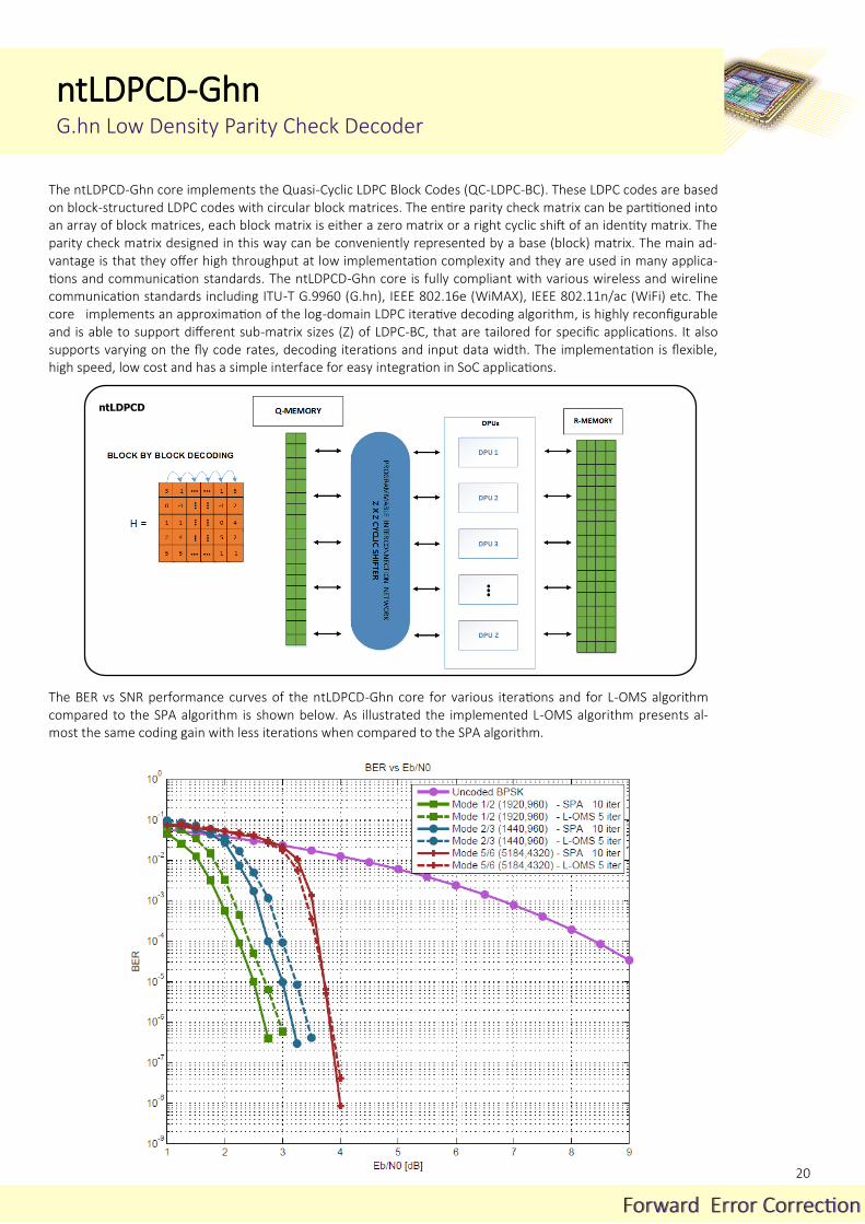
The ntLDPCE-Ghn core implements the Quasi-Cyclic LDPC Block Codes (QC-LDPC-BC). These LDPC codes are based on block-structured LDPC codes with circular block matrices. The entire parity check matrix can be partitioned into an array of block matrices, each block matrix is either a zero matrix or a right cyclic shift of an identity matrix. The parity check matrix designed in this way can be conveniently represented by a base (block) matrix. The main ad-vantage is that they offer high throughput at low implementation complexity and they are used in many applica-tions and communication standards. The ntLDPCE-Ghn core is fully compliant with various wireless and wireline communication standards including ITU-T G.9960 (G.hn), IEEE 802.16e (WiMAX), IEEE 802.11n/ac (WiFi) etc. The core is highly reconfigurable and is able to support different sub-matrix sizes (Z) of LDPC-BC, that are tailored for specific applications. It also supports varying on the fly code rates and input data width. The implementation is flexible, high speed, efficient area utilization and has a simple interface for easy integration in SoC applications.
Silicon Vendor Device Configuration Resources Fmax (MHz)
Xilinx Kintex 7
XC7K410T-2 ITU-T 9960 G.hn compliant 4250 Slices / 31 Block RAMs 203
The ntLDPCE-Ghn core has been synthesized using Xilinx ISE Design Suite tools. The core has been targeted to Kintex-7 XC7K410T-2 FFG900 device with a default balanced optimization strategy between area and timing. The implementation details and performance metrics of the ntLDPCE core configured for ITU-T 9960 G.hn standard are shown in the tables below.
Mode Code Rate
Throughput Rate (Gbps) Z-bits parallelism
Throughput Rate (Gbps) 8-bits parallelism
(code_len, info_len)
1 (1/2)H 0.310 0.272 (336,168)
2 (1/2)S 1.355 0.748 (1920,960)
3 (1/2)L (8640,4320) 1.458 0.745
4 (2/3)S (1439,960) 1.397 0.998
5 (2/3)L (6480,4320) 1.447 0.980
6 (5/6)S (1152,960) 1.442 1.249
7 (5/6)L (5184,4320) 1.479 1.243
Memory Unit
RFD_ENC
Z_MOD_O
DVAL
DOUT
ntLDPCE
Z_MOD_I
RFD
DRS
DIN
CLK
RSTB
SRST
Cyclic
Shifter
Unit
Accummulator
Unit
XOR
Unit
CEN
Controller Unit
20
Forward Error CorrectionForward Error Correction
ntLDPCD-Ghn G.hn Low Density Parity Check Decoder
The ntLDPCD-Ghn core implements the Quasi-Cyclic LDPC Block Codes (QC-LDPC-BC). These LDPC codes are based on block-structured LDPC codes with circular block matrices. The entire parity check matrix can be partitioned into an array of block matrices, each block matrix is either a zero matrix or a right cyclic shift of an identity matrix. The parity check matrix designed in this way can be conveniently represented by a base (block) matrix. The main ad-vantage is that they offer high throughput at low implementation complexity and they are used in many applica-tions and communication standards. The ntLDPCD-Ghn core is fully compliant with various wireless and wireline communication standards including ITU-T G.9960 (G.hn), IEEE 802.16e (WiMAX), IEEE 802.11n/ac (WiFi) etc. The core implements an approximation of the log-domain LDPC iterative decoding algorithm, is highly reconfigurable and is able to support different sub-matrix sizes (Z) of LDPC-BC, that are tailored for specific applications. It also supports varying on the fly code rates, decoding iterations and input data width. The implementation is flexible, high speed, low cost and has a simple interface for easy integration in SoC applications.
ntLDPCD
The BER vs SNR performance curves of the ntLDPCD-Ghn core for various iterations and for L-OMS algorithm compared to the SPA algorithm is shown below. As illustrated the implemented L-OMS algorithm presents al-most the same coding gain with less iterations when compared to the SPA algorithm.

21
ntLDPCE-DVB-S2 DVB S2 Low Density Parity Check Encoder
Forward Error CorrectionForward Error Correction
ntLDPCE-DVB-S2
Controller
DINDRSMODE
RFD_ENCDOUTDVAL
XOR Accumulators
Memory
Cyclic Shifter
CLKRST_N
BLKSBLKE
The ntLDPCE-DVB-S2 IP Core implements the encoding procedure for LDPC Block Codes (LDPC-BC) or QC-LDPC Quasi-Cyclic LDPC Codes compliant with the DVB-S2 standard. These LDPC codes are transformed to approximate block-structured LDPC codes with circular block matrices. The entire parity check matrix can be partitioned into an array of block matrices; each block matrix is either a zero matrix or a right cyclic shift of an identity matrix. The parity check matrix pre-processed in this way can be conveniently represented by a base matrix represented by cyclic shifts. The core is highly reconfigurable and it is able to support the sub-matrix size (Z=360) of QC-LDPC, that is tailored for the DVB-S2 standard. The ntLDPCE-DVB-S2 Encoder has partial parallel architecture and supports Z=360 parallel input bits per clock cy-cle. The encoder receives information data, generates the parity bits and forms the codeword that will be trans-mitted. A selected mode requires K_LDPC/Z clock cycles in order to feed the encoder with a single block of infor-mation. The encoder architecture input is configured to support double buffering.
The ntLDPCE-DVB-S2 core has been synthesized using Xilinx Vivado Design Suite tools. The core has been targeted to Kintex-7 XC7K410T-2 FFG900 device with a default balanced optimization strategy between area and timing. The implementation details and performance metrics of the ntLDPCE-DVB-S2 core configured for DVB S2 standard are shown in the tables below.
The following table demonstrates the DVB-S2 encoding modes of operation.
Mode Codeword size DVB S2 Mode (R=K/N) Mode Codeword size DVB S2 Mode (R=K/N)
0 16200 DVB S2 1/4 (R=1/5) 11 64800 DVB S2 2/3
1 64800 DVB S2 1/4 12 16200 DVB S2 3/4 (R=11/15)
2 16200 DVB S2 1/3 13 64800 DVB S2 3/4
3 64800 DVB S2 1/3 14 16200 DVB S2 4/5 (R=7/9)
4 16200 DVB S2 2/5 15 64800 DVB S2 4/5
5 64800 DVB S2 2/5 16 16200 DVB S2 5/6 (R=2=37/45)
6 16200 DVB S2 1/4 (R=4/9) 17 64800 DVB S2 5/6
7 64800 DVB S2 1/2 18 16200 DVB S2 8/9
8 16200 DVB S2 3/5 19 64800 DVB S2 8/9
9 64800 DVB S2 3/5 20 - RESERVED
10 16200 DVB S2 2/3 21 64800 DVB S2 9/10
Silicon Vendor Device Configuration Resources Fmax (MHz)
Xilinx Kintex 7
XC7K410T-2 DVB-S2 compliant 3615 FFs / 13485 LUTs / 222 Block RAMs 140
22
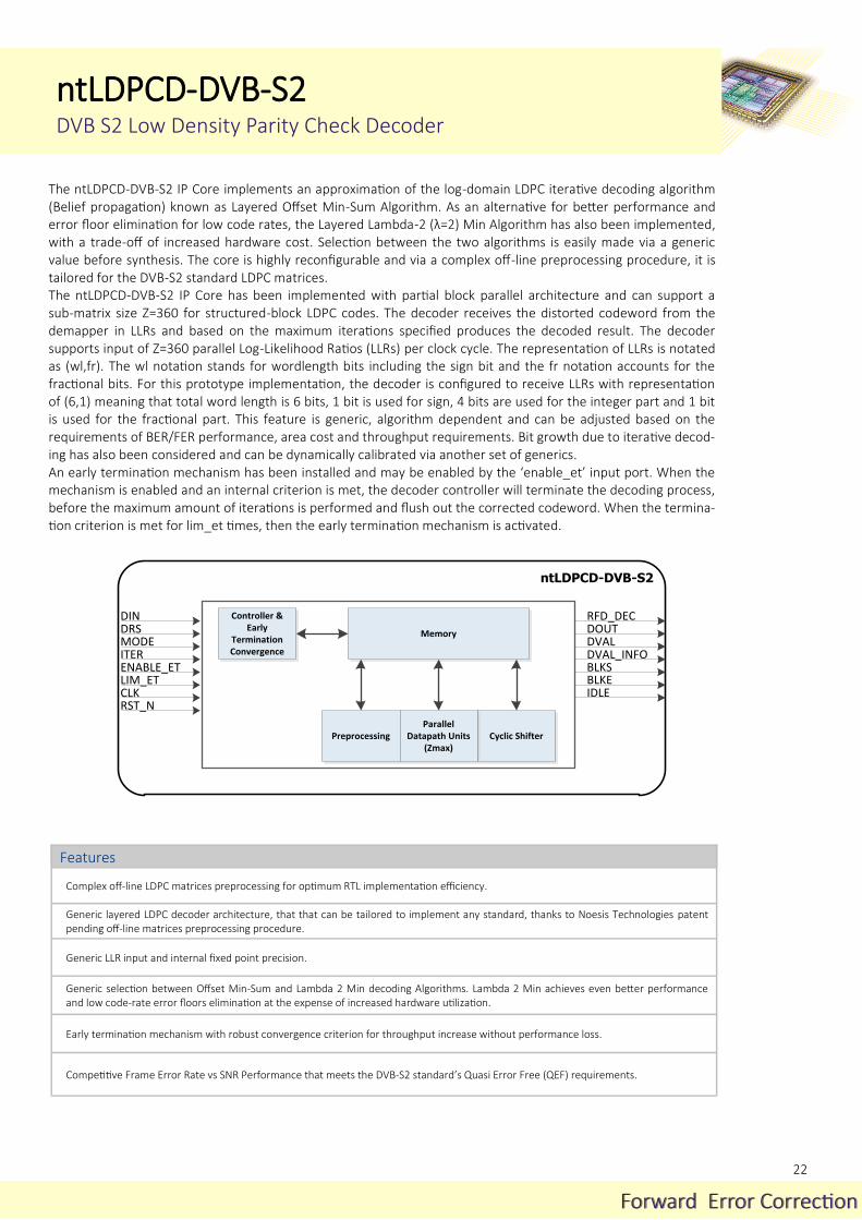
ntLDPCD-DVB-S2 DVB S2 Low Density Parity Check Decoder
Forward Error CorrectionForward Error Correction
The ntLDPCD-DVB-S2 IP Core implements an approximation of the log-domain LDPC iterative decoding algorithm (Belief propagation) known as Layered Offset Min-Sum Algorithm. As an alternative for better performance and error floor elimination for low code rates, the Layered Lambda-2 (λ=2) Min Algorithm has also been implemented, with a trade-off of increased hardware cost. Selection between the two algorithms is easily made via a generic value before synthesis. The core is highly reconfigurable and via a complex off-line preprocessing procedure, it is tailored for the DVB-S2 standard LDPC matrices. The ntLDPCD-DVB-S2 IP Core has been implemented with partial block parallel architecture and can support a sub-matrix size Z=360 for structured-block LDPC codes. The decoder receives the distorted codeword from the demapper in LLRs and based on the maximum iterations specified produces the decoded result. The decoder supports input of Z=360 parallel Log-Likelihood Ratios (LLRs) per clock cycle. The representation of LLRs is notated as (wl,fr). The wl notation stands for wordlength bits including the sign bit and the fr notation accounts for the fractional bits. For this prototype implementation, the decoder is configured to receive LLRs with representation of (6,1) meaning that total word length is 6 bits, 1 bit is used for sign, 4 bits are used for the integer part and 1 bit is used for the fractional part. This feature is generic, algorithm dependent and can be adjusted based on the requirements of BER/FER performance, area cost and throughput requirements. Bit growth due to iterative decod-ing has also been considered and can be dynamically calibrated via another set of generics. An early termination mechanism has been installed and may be enabled by the ‘enable_et’ input port. When the mechanism is enabled and an internal criterion is met, the decoder controller will terminate the decoding process, before the maximum amount of iterations is performed and flush out the corrected codeword. When the termina-tion criterion is met for lim_et times, then the early termination mechanism is activated.
Features
Complex off-line LDPC matrices preprocessing for optimum RTL implementation efficiency.
Generic layered LDPC decoder architecture, that that can be tailored to implement any standard, thanks to Noesis Technologies patent pending off-line matrices preprocessing procedure.
Generic LLR input and internal fixed point precision.
Generic selection between Offset Min-Sum and Lambda 2 Min decoding Algorithms. Lambda 2 Min achieves even better performance and low code-rate error floors elimination at the expense of increased hardware utilization.
Early termination mechanism with robust convergence criterion for throughput increase without performance loss.
Competitive Frame Error Rate vs SNR Performance that meets the DVB-S2 standard’s Quasi Error Free (QEF) requirements.
ntLDPCD-DVB-S2
Controller & Early
TerminationConvergence
DINDRSMODE
RFD_DECDOUTDVAL
Preprocessing
Memory
Cyclic Shifter
CLKRST_N
DVAL_INFOBLKS
ParallelDatapath Units
(Zmax)
ITERENABLE_ETLIM_ET BLKE
IDLE

23
ntLDPCD-DVB-S2 DVB S2 Low Density Parity Check Decoder
Forward Error CorrectionForward Error Correction
The ntLDPCD-DVB-S2 core has been synthesized using Xilinx Vivado Design Suite tools. The core has been targeted to Kintex-7 XC7K410T-2 FFG900 device with a default balanced optimization strategy between area and timing. The implementation details and performance metrics of the ntLDPCD-DVB-S2 core configured for DVB S2 standard are shown in the tables below.
Silicon Vendor Device Algorithm Config Resources Fmax (MHz)
Xilinx Kintex 7
XC7K410T-2 Offset Min Sum 35204 FFs / 116805 LUTs / 320 Block RAMs 50
Xilinx Kintex 7
XC7K410T-2 λ Min 37391 FFs / 131164 LUTs / 320 Block RAMs 50
The ntLDPCD-DVB-S2 achieves exceptional error correction performance as illustrated in the following FER vs Es/No graphs for all modes of operation as described in DVB S2 specification. The measurement conditions were as follows: □ Input LLR S6.1 (signed, 4 integer bits, 1 fractional bit) □ Approximate LLR calculation without proportional σ**2 scaling □ AWGN channel impairments □ QPSK modulation □ Early Termination enabled after 4 converging iterations □ Concatenation with outer 0.99 code rate block code
24
ntLDPCE-DVB-S2X DVB S2X Low Density Parity Check Encoder
Forward Error CorrectionForward Error Correction
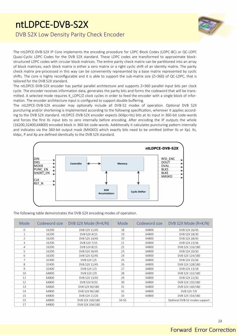
The ntLDPCE-DVB-S2X IP Core implements the encoding procedure for LDPC Block Codes (LDPC-BC) or QC-LDPC Quasi-Cyclic LDPC Codes for the DVB S2X standard. These LDPC codes are transformed to approximate block-structured LDPC codes with circular block matrices. The entire parity check matrix can be partitioned into an array of block matrices; each block matrix is either a zero matrix or a right cyclic shift of an identity matrix. The parity check matrix pre-processed in this way can be conveniently represented by a base matrix represented by cyclic shifts. The core is highly reconfigurable and it is able to support the sub-matrix size (Z=360) of QC-LDPC, that is tailored for the DVB S2X standard. The ntLDPCE-DVB-S2X encoder has partial parallel architecture and supports Z=360 parallel input bits per clock cycle. The encoder receives information data, generates the parity bits and forms the codeword that will be trans-mitted. A selected mode requires K_LDPC/Z clock cycles in order to feed the encoder with a single block of infor-mation. The encoder architecture input is configured to support double buffering. The ntLDPCE-DVB-S2X encoder may optionally include all DVB-S2 modes of operation. Optional DVB S2X puncturing and/or shortening is implemented according to the following specification, wherever it applies accord-ing to the DVB S2X standard. ntLDPCE-DVB-S2X encoder expects (kldpc+Xs) bits at its input in 360-bit code-words and forces the first Xs input bits to zero internally before encoding. After encoding the IP outputs the whole (16200,32400,64800) encoded block in 360-bit code-words. Additionally it calculates puncturing pattern internally and indicates via the 360-bit output mask (MASKO) which exactly bits need to be omitted (either Xs or Xp). Xs, kldpc, P and Xp are defined identically to the DVB S2X standard.
Controller
DIN DRS MODE PUNC_EN SHORT_EN
RFD_ENCDOUTDVAL
XOR Accumulators
Memory
Cyclic Shifter
CLK RST_N
BLKSBLKEMASKO
ntLDPCE-DVB-S2X
The following table demonstrates the DVB-S2X encoding modes of operation.
Mode Codeword size DVB S2X Mode (R=K/N) Mode Codeword size DVB S2X Mode (R=K/N)
0 16200 DVB S2X 11/45 18 64800 DVB S2X 26/45
1 16200 DVB S2X 4/15 19 64800 DVB S2X 18/30
2 16200 DVB S2X 14/45 20 64800 DVB S2X 28/45
3 16200 DVB S2X 7/15 21 64800 DVB S2X 23/36
4 16200 DVB S2X 8/15 22 64800 DVB S2X 116/180
5 16200 DVB S2X 26/45 23 64800 DVB S2X 20/30
6 16200 DVB S2X 32/45 24 64800 DVB S2X 124/180
7 32400 DVB S2X 1/5 25 64800 DVB S2X 25/36
8 32400 DVB S2X 11/45 26 64800 DVB S2X 128/180
9 32400 DVB S2X 1/3 27 64800 DVB S2X 13/18
10 64800 DVB S2X 2/9 28 64800 DVB S2X 132/180
11 64800 DVB S2X 13/45 29 64800 DVB S2X 22/30
12 64800 DVB S2X 9/20 30 64800 DVB S2X 135/180
13 64800 DVB S2X 90/180 31 64800 DVB S2X 140/180
14 64800 DVB S2X 96/180 32 64800 DVB S2X 7/9
15 64800 DVB S2X 11/20 33 64800 DVB S2X 154/180
15 64800 DVB S2X 100/180 34-55 - Optional DVB-S2 modes support
17 64800 DVB S2X 104/180

25
ntLDPCE-DVB-S2X DVB S2X Low Density Parity Check Encoder
Forward Error CorrectionForward Error Correction
The ntLDPCE-DVB-S2X core has been synthesized using Xilinx Vivado Design Suite tools. The core has been targeted to Kintex-7 XC7K410T-2 FFG900 device with a default balanced optimization strategy between area and timing. The implementation details and performance metrics of the ntLDPCE-DVB-S2X core configured for DVB S2X standard are shown in the tables below.
Silicon Vendor Device Configuration Resources Fmax (MHz)
Xilinx Kintex 7
XC7K410T-2 DVB-S2X compliant 3615 FFs / 13485 LUTs / 222 Block RAMs 140

26
ntLDPCD-DVB-S2X DVB S2X Low Density Parity Check Decoder
Forward Error CorrectionForward Error Correction
The ntLDPCD-DVB-S2X IP Core implements an approximation of the log-domain LDPC iterative decoding algorithm (Belief propagation) known as Layered Offset Min-Sum Algorithm. As an alternative for better performance and error floor elimination for low code rates, the Layered Lambda-2 (λ=2) Min Algorithm has also been implemented, with a trade-off of increased hardware cost. Selection between the two algorithms is easily made via a generic value before synthesis. The core is highly reconfigurable and via a complex off-line preprocessing procedure, it is tailored for the DVB-S2X standard LDPC matrices. The ntLDPCD-DVB-S2X IP Core has been implemented with partial block parallel architecture and can support a sub-matrix size Z=360 for structured-block LDPC codes. The decoder receives the distorted codeword from the demapper in LLRs and based on the maximum iterations specified produces the decoded result. The decoder supports input of Z=360 parallel Log-Likelihood Ratios (LLRs) per clock cycle. The representation of LLRs is notated as (wl,fr). The wl notation stands for wordlength bits including the sign bit and the fr notation accounts for the fractional bits. For this prototype implementation, the decoder is configured to receive LLRs with representation of (6,1) meaning that total word length is 6 bits, 1 bit is used for sign, 4 bits are used for the integer part and 1 bit is used for the fractional part. This feature is generic, algorithm dependent and can be adjusted based on the requirements of BER/FER performance, area cost and throughput requirements. Bit growth due to iterative decoding has also been considered and can be dynamically calibrated via another set of generics. An early termination mechanism has been installed and may be enabled by the ‘enable_et’ input port. When the mechanism is enabled and an internal criterion is met, the decoder controller will terminate the decoding process, before the maximum amount of iterations is performed and flush out the corrected codeword. When the termination criterion is met for lim_et times, then the early termination mechanism is activated. The ntLDPCD-DVB-S2X decoder may optionally include all DVB-S2 modes of operation.
Features
Complex off-line LDPC matrices preprocessing for optimum RTL implementation efficiency.
Generic layered LDPC decoder architecture, that that can be tailored to implement any standard, thanks to Noesis Technologies patent pending off-line matrices preprocessing procedure.
Generic LLR input and internal fixed point precision.
Generic selection between Offset Min-Sum and Lambda 2 Min decoding Algorithms. Lambda 2 Min achieves even better performance and low code-rate error floors elimination at the expense of increased hardware utilization.
Early termination mechanism with robust convergence criterion for throughput increase without performance loss.
Competitive Frame Error Rate vs SNR Performance that meets the DVB-S2 standard’s Quasi Error Free (QEF) requirements.
IP may also be backwards compatible with all DVB-S2 LDPC modes.
ntLDPCD-DVB-S2X
Controller & Early
TerminationConvergence
DINDRSMODE
RFD_DECDOUTDVAL
Preprocessing
Memory
Cyclic Shifter
CLKRST_N
DVAL_INFOBLKS
ParallelDatapath Units
(Zmax)
ITERENABLE_ETLIM_ET BLKE
IDLE

27
ntLDPCD-DVB-S2X DVB S2X Low Density Parity Check Decoder
Forward Error CorrectionForward Error Correction
The ntLDPCD-DVB-S2X core has been synthesized using Xilinx Vivado Design Suite tools. The core has been targeted to Kintex-7 XC7K410T-2 FFG900 device with a default balanced optimization strategy between area and timing. The implementation details and performance metrics of the ntLDPCD-DVB-S2X core configured for DVB S2X standard are shown in the tables below.
Silicon Vendor Device Algorithm Config Resources Fmax (MHz)
Xilinx Kintex 7
XC7K410T-2 Offset Min Sum 35204 FFs / 116805 LUTs / 320 Block RAMs 50
Xilinx Kintex 7
XC7K410T-2 λ Min 37391 FFs / 131164 LUTs / 320 Block RAMs 50
The ntLDPCD-DVB-S2X achieves exceptional error correction performance as illustrated in the following FER vs Es/No graphs for all modes of operation as described in DVB S2X specification. The measurement condi-tions were as follows: □ Input LLR S6.1 (signed, 4 integer bits, 1 fractional bit) □ Approximate LLR calculation without proportional σ**2 scaling □ AWGN channel impairments □ QPSK modulation □ Early Termination enabled after 4 converging iterations □ Concatenation with outer 0.99 code rate block code

28
Forward Error CorrectionForward Error Correction
ntINT_DEINT Fully Configurable Interleaver—Deinterleaver
The ntINT_DEINT core has been targeted to both ASIC and FPGA technologies for various applications. Noesis Technologies can also deliver netlist versions of the core optimized to specific area resources and performance requirements.
Error detection and correction are perhaps the most important quality factors to observe when evaluating a digital transmission system. A system’s noise environment can cause errors in the transmitted message degrading the credibility of the system. Digital communications systems designers can choose among many types of error-correction codes to reduce the effect of errors in stored or transmitted data. Most common error correcting codes are designed to correct random errors i.e. errors that are independent of each other and distributed uniformly in time. However errors that occur in bursts ,i.e. errors that occur sequentially in time and as groups, tend to be problematic for most FEC schemes. Block codes, and in particular Reed-Solomon codes, can handle burst errors effectively only as long as the number of errors per data block is below a certain limit. Interleaving is a simple, yet powerful technique that can be used to extend the error correcting capability of a Reed-Solomon code and other FEC codes. The ntINT_DEINT interleaver/de-interleaver subsystem rearranges the encoded symbols over multiple data blocks. This effectively spreads out long burst noise sequences so they appear to the decoder as independent random symbol errors or shorter more manageable burst errors. This is achieved by using the interleaving function that changes the order of data before the transmission on the channel so that any adjacent symbols are well separated during transmission. The symbols are then reordered by the dein-terleaving function during reception. Block and Convolutional are the most frequently used interleaver types.
Silicon Vendor
Device Resources Fmax (MHz)
Configuration
Xilinx Kintex 7
XC7K410T-2 253 Slices / 3 Block RAMs 157
Convolutional / NUMBITS=8 MAX_BRN_NUM=4 / MAX_UNIT_DEL=4
Xilinx Kintex 7
XC7K410T-2 744 Slices / 13 Block RAMs
1 DSP48E1 132
Convolutional / NUMBITS=16 MAX_BRN_NUM=16 / MAX_UNIT_DEL=16
Xilinx Kintex 7
XC7K410T-2 Convolutional / NUMBITS=8
MAX_BRN_NUM=32 / MAX_UNIT_DEL=32 1276 Slices / 31 Block RAMs
1 DSP48E1 124
Xilinx Kintex 7
XC7K410T-2 Block / NUMBITS=8 / MAX_ROW_NUM=32 MAX_COL_NUM=32 / MAX_PREM_NUM=4
185 Slices / 4 Block RAMs 261
Xilinx Kintex 7
XC7K410T-2 Block / NUMBITS=16 / MAX_ROW_NUM=64 MAX_COL_NUM=64 / MAX_PREM_NUM=4
246 Slices / 6 Block RAMs 226
Xilinx Kintex 7
XC7K410T-2 Block / NUMBITS=64 / MAX_ROW_NUM=128 MAX_COL_NUM=128 / MAX_PREM_NUM=4
320 Slices / 66 Block RAMs 1 DSP48E1
166
Features
Fully configurable, convolutional and rectangu-lar interleaver / deinterleaver.
Compliant to a variety of industry standards such as DVB, ATSC, IEEE 802.16. etc.
Rectangular Block (de) interleaver configura-tion: - Block size - Number of rows - Number of columns - Rows and/or columns permutations
Convolutional (de) interleaver configuration: - Number of branches - Configurable branch length
Supports continuous block data flow.
Configurable number of bits per symbol.
Handshaking logic for I/O data flow control.
Fully synchronous design, using single clock.
Silicon proven in ASIC and Xilinx FPGA imple-mentation technologies for a variety of applica-tions.
Memory Unit
ntINT_DEINT
DIN Controller Unit
CLK
RSTB
SRST
CEN
DRS
BLKSTRT_I
BLKEND_I
ROW_NUM
COL_NUM
ROW_PAT
COL_PAT
PERM_SEL
PERM_SEL_PRG
PROG_CLR
BRN_NUM
UNIT_DEL
MODE DOUT
DVAL
BLKSTRT_O
BLKEND_O
RDY

29
Voice compression technology is widely used in digital communication systems such as wireless systems, VoIP, and video conference technology. Voice com-pression reduces data redundancy and thus eases bandwidth requirements. The International Telecommunication Union (ITU) has standardized a number of speech compression algorithms for a variety of compression rates as well as Mean Opinion Scores (MOS). Noesis Technologies provides a series of silicon IPs of the most popular voice codecs (G711, G726, G729, CVSD), providing com-pression rates ranging from 64 kbps down to 8 kbps. In addition, Noesis Technologies offers a proprietary implementation of Huffman block differential lossless data compression algorithm. This core is ideal for use in low power applications like Wireless Sensor Networks (WSN) as well as any other application with slow changing nature of data, to fully benefit from the differential nature of the algorithm.
Voice & Data Compression

30
Voice & Data CompressionVoice & Data Compression
ntG711 A/u Law Codec— ITU-T G711 compliant
The ntG711 core implements the ITU G.711 compliant compressing and expanding functions. It is comprised of a compressor and an expander unit. The compressor unit performs compression of the 16-bit uniform PCM to a 8-bit A/μ-law word. The expander unit decompresses the 8-bit A/μ-law to 14-bit uniform PCM word. The ntG711 core is programmable and its functionality is controlled by the following control bits. law : This bit selects the coding rule to be used. When ‘0’ μ-law is selected, when ‘1’ A-law is selected. A_inv_dis : This bit activates/disactivates the inversion of even bits of the input word for the A-law case. u_inv_dis : This bit activates/disactivates the inversion of bits of the input word for the μ-law case. comp_dis : This bit selects the representation format of the output vector. When ‘0’ is in 2’s complement format, when ‘1’ is in sign magnitude format. The ntG711 core can be used in a variety of applications, including PCM codecs, voice compression and expanding as well as a front–end for any DSP processing of 64 kbps voice.
Silicon Vendor Device Resources Fmax (MHz)
Xilinx Virtex-5 54 CLB Slices (Compressor unit)
75 CLB Slices / 1 DSP48E (Expander unit) 115 MHz
TSMC 180 nm 610 gates (Compressor unit)
720 gates (Expander Unit)
The ntG711 core has been targeted to both ASIC and FPGA technologies for various applications. Noesis Technologies can also deliver netlist versions of the core optimized to specific area resources and performance requirements.
-5000 -4000 -3000 -2000 -1000 0 1000 2000 3000 4000 5000-150
-100
-50
0
50
100
150
-1 -0.8 -0.6 -0.4 -0.2 0 0.2 0.4 0.6 0.8 1
x 104
-150
-100
-50
0
50
100
150
-150 -100 -50 0 50 100 150-5000
-4000
-3000
-2000
-1000
0
1000
2000
3000
4000
5000
-150 -100 -50 0 50 100 150-1
-0.8
-0.6
-0.4
-0.2
0
0.2
0.4
0.6
0.8
1x 10
4
The PCM to A-law and to μ-law transformation
A-law and μ-law to PCM transformation
Law_in
Data_in(15-0)
Data_out(7:0)
A_inv_dis_in
U_inv_dis_in
Compl_dis_in
A/μ-LawCompressor
Law_in
Data_in(7:0)
Data_out(13:0)
A_inv_dis_in
U_inv_dis_in
Compl_dis_in
A/μ-LawExpander
Data_out_scaled(16:0)
Gain_en(1:0)
31
Voice & Data CompressionVoice & Data Compression
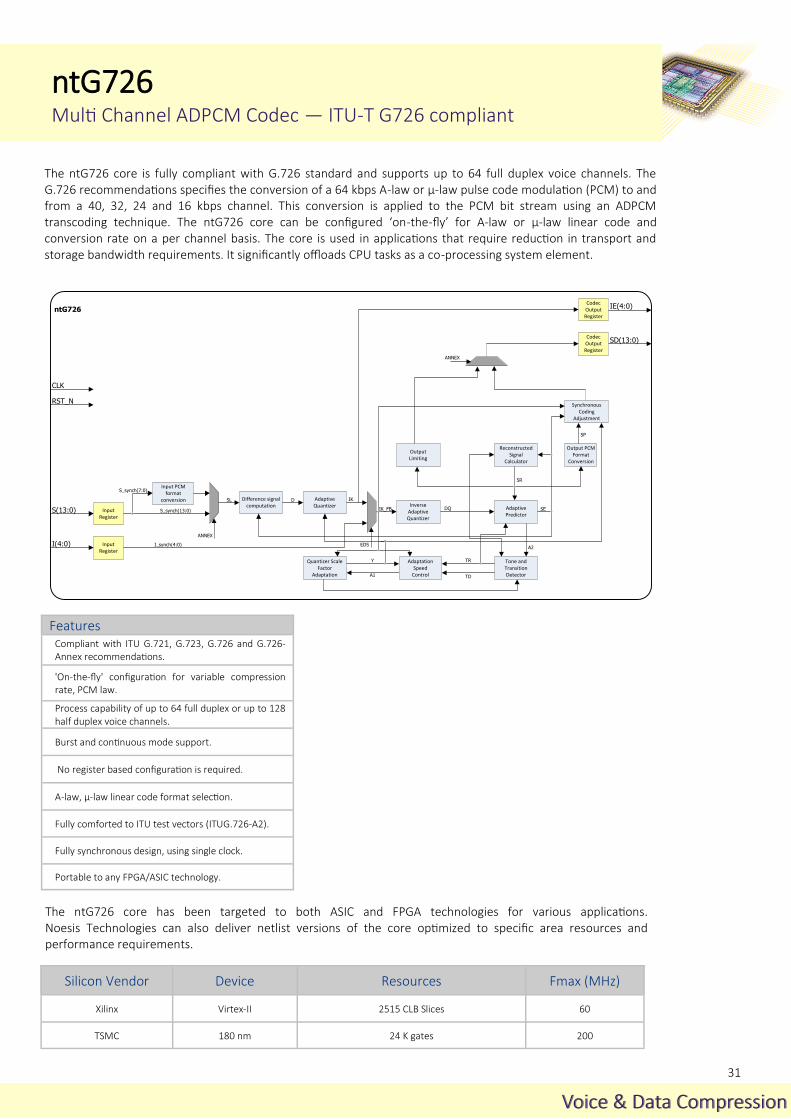
ntG726 Multi Channel ADPCM Codec — ITU-T G726 compliant
The ntG726 core is fully compliant with G.726 standard and supports up to 64 full duplex voice channels. The G.726 recommendations specifies the conversion of a 64 kbps A-law or μ-law pulse code modulation (PCM) to and from a 40, 32, 24 and 16 kbps channel. This conversion is applied to the PCM bit stream using an ADPCM transcoding technique. The ntG726 core can be configured ‘on-the-fly’ for A-law or μ-law linear code and conversion rate on a per channel basis. The core is used in applications that require reduction in transport and storage bandwidth requirements. It significantly offloads CPU tasks as a co-processing system element.
Features Compliant with ITU G.721, G.723, G.726 and G.726-Annex recommendations.
'On-the-fly' configuration for variable compression rate, PCM law.
Process capability of up to 64 full duplex or up to 128 half duplex voice channels.
Burst and continuous mode support.
No register based configuration is required.
A-law, μ-law linear code format selection.
Fully comforted to ITU test vectors (ITUG.726-A2).
Fully synchronous design, using single clock.
Portable to any FPGA/ASIC technology.
Silicon Vendor Device Resources Fmax (MHz)
Xilinx Virtex-II 2515 CLB Slices 60
TSMC 180 nm 24 K gates 200
InputRegister
InputRegister
S(13:0)
I(4:0)
Input PCM format
conversion
S_synch(13:0)
S_synch(7:0)
SL Difference signalcomputation
D AdaptiveQuantizer
ANNEX
EDSI_synch(4:0)
Quantizer ScaleFactor
Adaptation
Y AdaptationSpeed
ControlA1
Tone andTransitionDetectorTD
TR
InverseAdaptiveQuantizer
IK_FB AdaptivePredictor
DQ
A2
ReconstructedSignal
Calculator
SR
OutputLimiting
Output PCMFormat
Conversion
SynchronousCoding
Adjustment
SP
IK
SE
CodecOutputRegister
CodecOutputRegister
SD(13:0)
IE(4:0)
CLK
RST_N
ntG726
ANNEX
The ntG726 core has been targeted to both ASIC and FPGA technologies for various applications. Noesis Technologies can also deliver netlist versions of the core optimized to specific area resources and performance requirements.

32
Voice & Data CompressionVoice & Data Compression
ntG729 Multi Channel CS-ACELP 8 kbps Codec — ITU-T G729A compliant
The growth in wireless communication systems, cellular mobile radio and VoIP technology has created the impera-tive need for bandwidth efficient, high speed quality voice coding algorithms. The ITU-T G.729 CS-ACELP is a high speech quality, low-bit rate (8kbps) codec that has been proposed to meet the voice compression requirements of a modern communication system. However the real time SW implementation of a multi-channel ITU-T G.729 com-pliant voice codec in conventional DSP processors is prohibitive due to the intensive amount of signal processing power required by the algorithm. To overcome this limitation Noesis Technologies has developed a revolutionized, highly efficient hybrid architecture that implements real time multi-channel G729A voice coding and exhibits the best performance-silicon area ratio available in the industry. The ntG729 IP Core can be used as a coprocessor to any processor type and can save significant computing resources for the main processor by efficiently executing the computationally intensive speech coding G729A algorithmic operations.
CLK
CINI[5:0]
ntG729
ENC_DEC
CH_RST
LAST_FRM
DSTRBControl Unit
LD_FRM
INIT_DONE
CIDO[5:0]
DVAL_ENC
DVAL_DEC
Preprocessor
UnitParallel ALU
Hardware
Acceleration
Unit
Channel
Memory
Data
Memory
Controller
Data
Memory
Fast Access
Memory
CH_DATA[5:0]
IM_ADDR[12:0]
IM_CW[150:0]
Postprocessor
Unit
RST_N Control
Sequencer
Silicon Vendor Device Resources Fmax (MHz)
Xilinx Virtex-7 18K CLB Slices / 31 Block RAMs / 105 DSP Slices 117
The ntG729 core has been core has been implemented to Xilinx devices.
Features Voice codec capable of multi-channel 8kbps voice compression based on ITU-T G729A standard.
Selective Channel initialization.
AMBA bus support for easy SoC integration.
Outperforms by a factor of two by supporting twice as many voice channels.
It requires only half the gate count thus increasing power efficiency and reducing costs.
Best performance/silicon area ratio available in the industry.
Fully synchronous design, using single clock.
Portable to any FPGA/ASIC technology. CLK
CIN
I[5:0
]
ntG729 AXI4Wrapper
EN
C_D
EC
CH
_RST
LAST_FRM
DSTRB
LD
_FRM
INIT
_D
ON
E
CID
O[5
:0]
DVAL_EN
C
DVAL_D
EC
AXI4 Protocol
Controller
CH_DATAO[15:0]
IM_ADDR[12:0]
IM_CW[150:0]
RST_N
IRQ[15:0]
AXI WRITE ADDRESS CHANNELAXI WRITE DATA CHANNEL
AXI WRITE RESPONSE CHANNEL
AXI READ ADDRESS CHANNELAXI READ DATA CHANNEL
CH_DATAI[15:0]
Decoder
Input
FIFO
Encoder
Input
FIFO
ntG729 Command Encoder Decoder
Encoder
Output
FIFO
Decoder
Output
FIFO
ntG729 Codec
AXI4 Wrapper
Controller

33
ntCVSD Continuously variable slope delta modulation
The fundamental principle of the CVSD algorithm is the encoding of one bit per sample. For example an audio sig-nal sampled at 32 KHz will be compressed to 32 Kbps. The ntCVSD codec IP core can be configured to operate either as an encoder or as a decoder functional block. In encoder mode the core accepts input data at a rate of 8 KHz/128 Kbps or 16KHz/256Kbps and are sampled when the data strobe signal is asserted high. Higher input sampling data rates can also be supported with no up-sampling provision. The sampled input data can either be initially up-sampled to 64 KHz by using an interpolation filter in order to improve speech/audio quality before entering into the actual CVSD codec unit or can be just directly fed into the CVSD codec unit with no previous processing. These samples are then driven to a digital comparator in order to be compared with a reference signal value. If the input sample is greater than the reference signal then a logic 1 is transmitted and a step value is added on the reference signal. If the input sample is less than the reference signal then a logic 0 is transmitted and a step value is subtracted from the reference signal. The transmitted bits are also stored in an N-bit shift register. Depending on the shift register contents, a decision is made whether a slope overload has occurred and the step value is adjusted accordingly in order to keep up with the changing slope of the input waveform. Depending on both the digital comparator and the slope overload decisions, an integrator estimation is generated in order to approximate the previous input value and drive it back to the digital comparator. In decoder mode the core accepts the compressed bit-stream and the incoming bits are sampled when the data strobe signal is asserted high. The received bit-stream is fed directly to the N-bit shift register and depending on the shift register contents, a decision is made whether a slope overload has occurred. The uncompressed signal is reconstructed through the integrator unit. The reconstructed output will be either be fed into the decimation filter to be down-sampled at the original sampling rate and then driven at the output or will be just directly driven at the output with no previous processing. The ntCVSD codec is designed to compress 16-bit PCM speech/audio data for transmission in telecom networks or to decompress a received CVSD encoded bit-stream. It is compatible with legacy CVSD implementations and fully compliant with the Bluetooth CVSD specification.
Voice & Data CompressionVoice & Data Compression
DATA_ENC_OUTDATA_DEC_OUT
ENC_DECFS_8_16DATA_DEC_IN
RST_ENCLK_EN
DATA_ENC_IN
ntCVSD
Interpolator 8x
Interpolator 4x
Decimator 8x
Decimator 4x
Digital
Comparator
Shift
Register
Delta Step
Manager
Integrator
Manager
Controller
CLK64
DSRTB DVAL
Silicon Vendor Device Resources Fmax (MHz)
Xilinx Virtex-6 349 CLB Slices / 31 DSP Slices 95
The ntCVSD core has been core has been implemented to Xilinx devices.

34
Voice & Data CompressionVoice & Data Compression
ntHUFF Huffman algorithm compression engine
The ntHUFF compression module implements the Huffman Block differential compression algorithm. The core processes data blocks of 500 16-bit input samples “on the fly” with latency as little as 4 clock cycles. A small input buffer of configurable size stores incoming 16-bit samples and propagates them to the compression module when instructed by the local controller. Samples are propagated through the differential data path comprised of a subtractor and an absolute calculation unit. The absolute value of all samples is used to update a metric table with statistical information and is also used to produce the compressed output. This is the initialization phase of the system. When samples equal to the defined block size have been collected, the controller enters calculations phase and pauses further samples propagation to the rest of the system. The Huffman microprocessor unit calculates and produces the Huffman (S) table, based on the populated metric table, which will be applied on the next block of incoming data. The custom microprocessor functions with encoded operations designed to optimize this phase. The core of the Huffman algorithm is implemented by performing parallel memory accesses on a parallel memory. A 512x36 instruction memory drives the micro-processor to execute all real time Huffman algorithm calculations. Worst case processing latency due to iterative algorithm nature is calculated to 4175 clock cycles per block of 500 samples. Once the Huffman (S) table has been calculated, the controller resumes samples propagation through the differential data path and S is applied to the next block of incoming samples in order to produce the compressed output. When samples equal to the defined block size have been collected, the calculations phase is activated again and so on. A flush enable input port is provided, which applies zero padding on the last 32bit compressed output at the end of each data block. The ntHUFF IP Core can be used in wireless sensor networks, medical applications as well as any data compression application with slow changing nature of data, to fully benefit from the differential nature of the algorithm.
Silicon Vendor Device Resources Fmax (MHz)
Xilinx Spartan-3 1724 CLB Slices / 8 Block RAMs 63
The ntHUFF core has been core has been implemented to Xilinx devices.
ntHUFF
RAW INPUT INPUT
BUFFER
REG
SUB ABSINT62LEC
UNIT
COMPRESSED OUTPUT
UPDATE
TABLE
UNIT
TABLE
REGF/MEM
S
REGF/MEM
HUFFMAN
UNIT
CONTROLLER

35
Noesis Technologies offers a range of security solutions ensuring privacy and authentication in digital transmissions. The Advanced Encryption Standard (AES) has been ratified in November 2001 by the National Institute of Standards and Technology (NIST) as the new encryption standard (FIPS PUB 197) to replace the existing, aging and vulnerable Data Encryption Standard (DES). An algorithm called Rinjdael has been finally selected for AES among a number of other can-didates, after successfully meeting a set of criteria including not only security but performance and implementation feasibility in a variety of applications. Noesis Technologies has been involved in the development of cryptographic solutions for telecom and defense sector since 2000 and its class leading solu-tions have been silicon proven in multiple applications. A wide range of AES cores have been designed to support different performance & silicon area com-binations that provide the optimum implementation for end-user application requirements. Due to a unique Galois Field Multiplier architectural implementa-tion, the structural datapath element of all AES cryptographic engines, and the highly efficient algorithmic mapping techniques the family of ntAES IP cores ex-hibit the best performance-silicon area ratio available in the industry. In addi-tion, Noesis Technologies provides SHA 256-bit authentication and RC4 encryp-tion IP cores for a various speed & silicon area application requirements.
Security

36
SecuritySecurity
ntAES8 AES Low Power Encryption/Decryption Engine
ntAES8 core implements the NIST FIPS-197 Advanced Encryption Standard and can be programmed to either en-crypt or decrypt 128-bit blocks of data using a 128-bit, 192-bit or 256-bit key. The ntAES8 has been carefully de-signed to require minimum logic resources rendering it an ideal solution for low power applications. This has been achieved by using an 8-bit data path size which means that 16 clock cycles are required to load/unload the 128-bit plaintext/ciphertext block. The encryptor receives the 128-bit plaintext block in 8-bit input symbols and generates the corresponding 128-bit ciphertext block in 8-bit output symbols using a supplied 128, 192, or 256-bit AES key. The pre-computed key values are read from an internal round key RAM. A key expander module is provided as an optional module to allow automatic generation and loading of the round key RAM. The decryptor implements the reverse function, generating plaintext from supplied ciphertext, using the same AES key as was used for encryp-tion. The implementation is very low on latency, high speed with a simple interface for easy integration in SoC applications. The ntAES8 core can be used in a variety of applications, including: - Electronic financial transactions. eCommerce, Banking, Securities exchange, Point-of-Sale - Secure communications. Storage Area Networks (SAN), Virtual Private Networks (VPN) Video Conferencing, Voice services - Secure environments. Satellite communications, Surveillance systems, Network appliances - Personal mobile communications. Video phones, PDA, Point-to-Point Wireless
State Address
Memory
KEYIN
KEY_WEN
KSS
DINVLD
ENCRYPT_REQENCRYPT_STATUS
DOUTRDY
Main
Control
Sub-Bytes Shift Rows Mix Columns
Key
Expander
KEY_ADDR
State
Memory
DOUT
DIN
Mix
Columns
Memory
Expanded
Keys
Memory
S-Box
Memory
ntAES8
Add
Round
Key
Silicon Vendor Device Resources Fmax (MHz)
Xilinx Spartan-3 160 CLB Slices / 1 Block RAM 200
TSMC 180 nm 1226 gates / 7680 RAM bits 515
The ntAES8 core has been core has been implemented to Xilinx devices as well as TSMC ASIC libraries.
Key size Throughput rate (Xilinx Spartan-3)
128 bits 53.3 Mbps
192 bits 44 Mbps
256 bits 37.4 Mbps

37
SecuritySecurity
ntAES32 AES High Speed Encryption/Decryption Engine
ntAES32 core implements the NIST FIPS-197 Advanced Encryption Standard and can be programmed to either encrypt or decrypt 128-bit blocks of data using a 128-bit, 192-bit or 256-bit key. The ntAES32 has been carefully designed for high throughput applications with optimal logic resources utilization. The encryptor core accepts a 128-bit plaintext input word, and generates a corresponding 128-bit ciphertext output word using a supplied 128, 192, or 256-bit AES key. The decryptor core provides the reverse function, generating plaintext from supplied ci-phertext, using the same AES key as was used for encryption. The hardware roundkey expansion logic has been designed as a discrete building block. This allows either to build a complete stand-alone AES solution, or to save logic resources by leaving the key generation process to the user. Alternatively, the roundkey expansion logic can be shared between multiple encryption/decryption cores for optimal silicon area resources utilization. The imple-mentation is very low on latency, high speed with a simple interface for easy integration in SoC applications. The ntAES32 core can be used in a variety of applications, including: - Electronic financial transactions. eCommerce, Banking, Securities exchange, Point-of-Sale - Secure communications. Storage Area Networks (SAN), Virtual Private Networks (VPN) Video Conferencing, Voice services - Secure environments. Satellite communications, Surveillance systems, Network appliances - Personal mobile communications. Video phones, PDA, Point-to-Point Wireless
Silicon Vendor Device Resources Fmax (MHz)
Xilinx Virtex-5 405 CLB Slices / 6 Block RAM 185
The ntAES32 core has been core has been implemented to Xilinx FPGA devices.
Key size Throughput rate (Xilinx Virtex-5)
128 bits 550 Mbps
192 bits 460 Mbps
256 bits 400 Mbps
State Address
Memory
KEYIN
KEY_WEN
KSS
DINVLD
ENCRYPT_REQENCRYPT_STATUS
DOUTRDY
Main
Control
Sub-Bytes Shift Rows Mix Columns
Key
Expander
KEY_ADDR
State
Memory
DOUT
DIN
Mix
Columns
Memory
Expanded
Keys
Memory
S-Box
Memory
ntAES32
Add
Round
Key

38
SecuritySecurity
ntAES128 AES Ultra High Speed Encryption/Decryption Engine
ntAES128 core implements the NIST FIPS-197 Advanced Encryption Standard and can be programmed to either encrypt or decrypt 128-bit blocks of data using a 128-bit, 192-bit or 256-bit key. The ntAES128 has been carefully designed for ultra high throughput applications with optimal logic resources utilization. The encryptor core ac-cepts a 128-bit plaintext input word, and generates a corresponding 128-bit ciphertext output word using a sup-plied 128, 192, or 256-bit AES key. The decryptor core provides the reverse function, generating plaintext from supplied ciphertext, using the same AES key as was used for encryption. The hardware roundkey expansion logic has been designed as a discrete building block. This allows either to build a complete stand-alone AES solution, or to save logic resources by leaving the key generation process to the user. Alternatively, the roundkey expansion logic can be shared between multiple encryption/decryption cores for optimal silicon area resources utilization. The implementation is very low on latency, high speed with a simple interface for easy integration in SoC applica-tions. The ntAES128 core can be used in a variety of applications, including: - Electronic financial transactions. eCommerce, Banking, Securities exchange, Point-of-Sale - Secure communications. Storage Area Networks (SAN), Virtual Private Networks (VPN) Video Conferencing, Voice services - Secure environments. Satellite communications, Surveillance systems, Network appliances - Personal mobile communications.
Silicon Vendor Device Resources Fmax (MHz)
Xilinx Kintex-7 570 CLB Slices / 8 Block RAMs 193
The ntAES128 core has been core has been implemented to Xilinx FPGA devices.
Key size Throughput rate (Xilinx Kintex-7)
128 bits 2.25 Gbps
192 bits 1.875 Gbps
256 bits 1.697 Gbps
State Address
Memory
KEYIN
KEY_WEN
KSS
DINVLD
ENCRYPT_REQENCRYPT_STATUS
DOUTRDY
Main
Control
Sub-Bytes Shift Rows Mix Columns
Key
Expander
KEY_ADDR
State
Memory
DOUT
DIN
Mix
Columns
Memory
Expanded
Keys
Memory
S-Box
Memory
ntAES128
Add
Round
Key
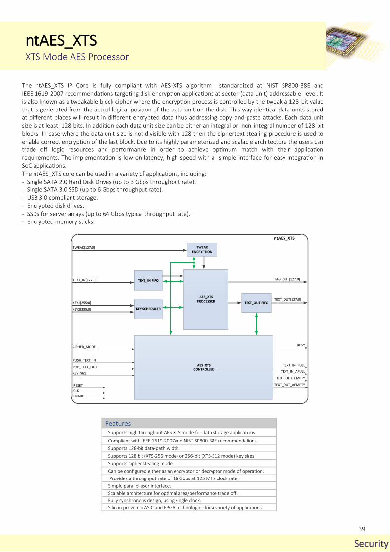
39
SecuritySecurity
ntAES_XTS XTS Mode AES Processor
The ntAES_XTS IP Core is fully compliant with AES-XTS algorithm standardized at NIST SP800-38E and IEEE 1619-2007 recommendations targeting disk encryption applications at sector (data unit) addressable level. It is also known as a tweakable block cipher where the encryption process is controlled by the tweak a 128-bit value that is generated from the actual logical position of the data unit on the disk. This way identical data units stored at different places will result in different encrypted data thus addressing copy-and-paste attacks. Each data unit size is at least 128-bits. In addition each data unit size can be either an integral or non-integral number of 128-bit blocks. In case where the data unit size is not divisible with 128 then the ciphertext stealing procedure is used to enable correct encryption of the last block. Due to its highly parameterized and scalable architecture the users can trade off logic resources and performance in order to achieve optimum match with their application requirements. The implementation is low on latency, high speed with a simple interface for easy integration in SoC applications. The ntAES_XTS core can be used in a variety of applications, including: - Single SATA 2.0 Hard Disk Drives (up to 3 Gbps throughput rate). - Single SATA 3.0 SSD (up to 6 Gbps throughput rate). - USB 3.0 compliant storage. - Encrypted disk drives. - SSDs for server arrays (up to 64 Gbps typical throughput rate). - Encrypted memory sticks.
KEY_SIZE
PUSH_TEXT_IN
RESET
CLK
ENABLE
TWEAKENCRYPTION
TEXT_IN[127:0]
TWEAK[127:0]
KEY SCHEDULER
KEY1[255:0]
KEY2[255:0]
AES_XTSPROCESSOR
TEXT_OUT[127:0]TEXT_OUT FIFO
AES_XTSCONTROLLER
BUSY
TAG_OUT[127:0]
TEXT_IN_FULL
TEXT_IN_AFULL
TEXT_OUT_EMPTY
TEXT_OUT_AEMPTY
CIPHER_MODE
POP_TEXT_OUT
ntAES_XTS
TEXT_IN FIFO
Features Supports high throughput AES XTS mode for data storage applications.
Compliant with IEEE 1619-2007and NIST SP800-38E recommendations.
Supports 128-bit data-path width.
Supports 128 bit (XTS-256 mode) or 256-bit (XTS-512 mode) key sizes.
Supports cipher stealing mode.
Can be configured either as an encryptor or decryptor mode of operation.
Provides a throughput rate of 16 Gbps at 125 MHz clock rate.
Simple parallel user interface.
Scalable architecture for optimal area/performance trade off.
Fully synchronous design, using single clock.
Silicon proven in ASIC and FPGA technologies for a variety of applications.
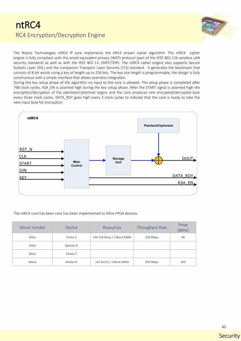
40
SecuritySecurity
ntRC4 RC4 Encryption/Decryption Engine
The Noesis Technologies ntRC4 IP core implements the ARC4 stream cipher algorithm. The ntRC4 cipher engine is fully compliant with the wired equivalent privacy (WEP) protocol (part of the IEEE 802.11b wireless LAN security standard) as well as with the IEEE 802.11i (WEP/TKIP). The ntRC4 cipher engine also supports Secure Sockets Layer (SSL) and the companion Transport Layer Security (TLS) standard. It generates the keystream that consists of 8-bit words using a key of length up to 256 bits. The key size length is programmable, the design is fully synchronous with a simple interface that allows seamless integration. During the key setup phase of the algorithm no input to the core is allowed. The setup phase is completed after 768 clock cycles. KSA_EN is asserted high during the key setup phase. After the START signal is asserted high the encryption/decryption of the plaintext/ciphertext begins and the core produces one encrypted/decrypted byte every three clock cycles. DATA_RDY goes high every 3 clock cycles to indicate that the core is ready to take the next input byte for encryption.
KEY
ntRC4
Main
Control
Plaintext/Ciphertext
Storage
Unit
DIN
START
CLK
RST_N
DOUT
DATA_RDY
KSA_EN
Silicon Vendor Device Resources Fmax (MHz)
Throughput Rate
Xilinx Virtex-2 134 CLB Slices / 2 Block RAMs 96 256 Mbps
Xilinx Spartan-6
Xilinx Kintex-7
Altera Stratix-IV 147 ALUTs / 2 Block RAMs 933 Mbps 350
The ntRC4 core has been core has been implemented to Xilinx FPGA devices.

41
SecuritySecurity
ntSHA256 SHA 256-bit Hash Generator
An n-bit hash is a map from arbitrary length messages to n-bit hash values. An n-bit cryptographic hash is an n-bit hash which is one-way and collision-resistant. Such functions are important cryptographic primitives used for such things as digital signatures and password protection. Current popular hashes produce hash values of length n = 128 (MD4 and MD5) and n = 160 (SHA-1), and therefore can provide no more than 64 or 80 bits of security, respectively, against collision attacks. Since the goal of the new Advanced Encryption Standard (AES) is to offer, at its three cryptovariable sizes, 128, 192, and 256 bits of security, there is a need for companion hash algorithms which provide similar levels of enhanced security. ntSHA256 IP Core implements SHA-256, or Secure Hash Algorithm-256 which is one of the latest hash functions standardized by the U.S. Federal Government. It is a 256-bit hash and is meant to provide 128 bits of security against collision attacks. The implementation is very low on latency, high speed with a simple interface for easy integration in SoC applications. The ntSHA256 core can used in a variety of applications, including: - Security applications and protocols (TLS, PGP, SSH, S/MIME, IPsec) - Authentication of Debian GNU/Linux software packages - DKIM message signing standard. - Transaction verification and proof-of-work calculation for several cryptocurrencies (Bitcoin). - Password protection - Digital signatures - Message authentication - Data integrity check
Silicon Vendor Device Resources Fmax (MHz)
Xilinx Spartan-3A 1577 CLB Slices / 1 Block RAM 50
The ntSHA256 core has been core has been implemented to Xilinx devices.
Block size Throughput rate
(Xilinx Spartan-3A)
512 bits 312 Mbps
ntSHA256
LENGTH COUNTER BIT PADDING
MAIN PADDING CONTROL
32 to 512 bit SIPO SHIFT REGISTERS
MESSAGE SCHEDULER
MESSAGE COMPRESSOR
MAIN SHA256 COMPRESSION
CONTROL
CONSTANT VALUES (k) TABLE
IN_DATA[31:0]
IN_VALID
LAST_BYTES[1:0]
LAST_WORD
HASH_OUT[255:0]
BLOCK_READY

42
Noesis Technologies offers an extensive library of state-of-the-art signal pro-cessing cores used at PHY level of a transmission system. Discrete Fourier Transforms (DFT) are very common in OFDM based wireless applications as well as in many other telecom applications. The Fast Fourier Transform (FFT) algorithm provides an efficient method for DFT computations in real-time applications. A fully configurable FFT/IFFT processor has been de-veloped that provides SoC designers with a range of high performance FFT cores for various target technologies and application requirements. The ntFFT IP Core employs a revolutionary parameterized architecture where the user can fine tune the level of data-path parallelism in order to achieve the optimum trade-off between silicon resources and throughput rate. A wide range of FFT lengths from 8-point to 8K-points is supported. Support for any power of 2 high-er than 8192 is also supported due to fully generic architecture. A fully configurable soft output demodulator has been designed that receives the equalized complex samples and converts them to a bit stream with soft out-put information associated with each bit. The probabilistic information is gener-ated based on LLR computations. The core also supports multiple PSK and QAM modulation levels and programmable number of soft bits. The performance evaluation of a telecom system under the presence of noise using software can be very time consuming. Whereas the noise generation in the analog domain is an easy task, in digital domain the generation of AWGN is a much more complex task. The ntAWGN core has been designed to provide a hardware implementation of an accurate AWGN noise generator that can be used in the efficient performance evaluation of a digital communication system. In addition Noesis Technologies provides customized IP Cores in the areas of channel equalization, channel estimation and synchronization.
Telecom DSP Functions

43
Telecom DSP FunctionsTelecom DSP Functions
ntFFT Fully Configurable FFT/IFFT Radix-2 Processor
ntFFT core is a fully configurable solution that performs the FFT and IFFT transform. It is on-the-fly programmable in terms of transform size and type. It supports complex input/output and the results are output in normal order. It exhibits a highly parameterizable/scalable design using generic I/O fixed point precision and generic internal calculations precision. The core uses fixed-point 2’s complement arithmetic with internal auto scaling to avoid arithmetic overflow and simplify dynamic range management. The ntFFT IP Core employs a revolutionary parameterized architecture where the user can fine tune the level of data-path parallelism in order to achieve the optimum trade-off between silicon resources and throughput rate. The implementation is portable to various silicon technologies, with a simple interface for easy integration in SoC applications.
Features
Radix-2 Fast Fourier Transform processor IP Core.
Same IP core may be used to compute both FFT and IFFT transforms without any complexity overhead.
Highly parameterizable/scalable design using generic I/O fixed point precision and generic internal calculations precision.
Bit true Matlab script model is provided to aid core fixed point precision configuration for any target application.
Tested against Matlab FFT and IFFT functions the ntFFT core produces fixed point numerical results with mean absolute error in range of 1e-4. The core may be parameterized for greater internal fixed point precision to lower the mean absolute error further.
Final fixed point scaling to avoid precision loss is performed internally.
Highly programmable design supporting all power of 2 FFT/IFFT transforms in range [8,…,MAX_NFFT], where MAX_NFFT=[8,…,8192]. Support for any power of 2 higher than 8192 is also possible.
Parameterized architectural parallelism level to meet any target application by tuning an effi-cient trade-off between utilized resources and maximum throughput rate.
Overclocked main memory at 2x rate to achieve minimum memory resources utilization.
Simple yet robust interface for optimum and efficient data flow control.
Optional AXI4-Stream protocol interface sup-port.
Fully synchronous design.
Silicon proven in ASIC and Xilinx FPGA imple-mentation technologies for a variety of applica-tions.
Silicon Vendor Device FFT size Resources Fmax (MHz)
Xilinx Kintex 7
XC7K410T-2 128
547 CLB Slices / 4 Block RAMs / 8 DSP48 Blocks
206
Xilinx Kintex 7
XC7K410T-2 512
716 CLB Slices / 5 Block RAMs / 8 DSP48 Blocks
190
Xilinx Kintex 7
XC7K410T-2 1024
652 CLB Slices / 6 Block RAMs / 12 DSP48 Blocks
171
Xilinx Kintex 7
XC7K410T-2 2048
765 CLB Slices / 16 Block RAMs / 16 DSP48 Blocks
170
Xilinx Kintex 7
XC7K410T-2 4096
745 CLB Slices/ 16 Block RAMs / 16 DSP48 Blocks
170
Xilinx Kintex 7
XC7K410T-2 8192
836 CLB Slices/ 33 Block RAMs / 16 DSP48 Blocks
166
The ntFFT core has been synthesized using Xilinx ISE Design Suite tools. The core has been targeted to Kintex-7 XC7K410T-2 FFG900 device with a default balanced optimization strategy between area and timing. The implementation details for various FFT sizes are shown in the table below.
The block diagram of the ntFFT elementary processing unit is shown in the figure below.
The modular architecture of the ntFFT processor is shown in the figure below.
FFT
Elementary
Processing
Unit #0
FFT
Elementary
Processing
Unit #0
FFT
Elementary
Processing
Unit #0
FFT
Elementary
Processing
Unit #0
CLKCLK2X
DQ
ntFFT
DI
CENS_RST
RST_N
DI_O
DQ_O
DVAL
BLKS_O
MODE
NFFT
BLKS
DRS Reform
Input
Input
Arbiter
FFT
Elementary
Processing
Unit #0
Output
ArbiterReform
Output
NFFT_O
IDLE
RFD
CLKCLK2X
DRS
ntFFT_EPU
DIN
CENS_RST
RST_N
RFD
DOUT
DVAL
BLKS_O
MODE
NFFT
BLKSEPU
Dataflow
Controller
NFFT_O
True
Quad
Port
RAM
Butterfly
Datapath
Unit
Twiddle
Factors
ROM
EPU
Post
Processor
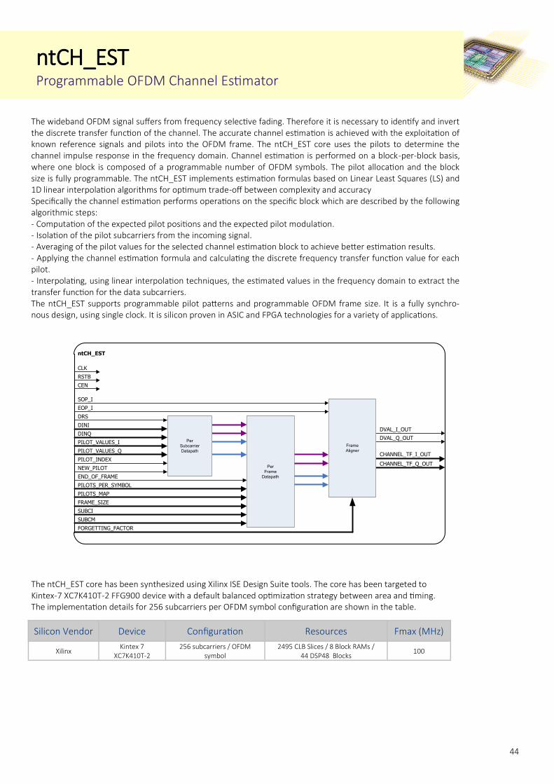
44
ntCH_EST Programmable OFDM Channel Estimator
The wideband OFDM signal suffers from frequency selective fading. Therefore it is necessary to identify and invert the discrete transfer function of the channel. The accurate channel estimation is achieved with the exploitation of known reference signals and pilots into the OFDM frame. The ntCH_EST core uses the pilots to determine the channel impulse response in the frequency domain. Channel estimation is performed on a block-per-block basis, where one block is composed of a programmable number of OFDM symbols. The pilot allocation and the block size is fully programmable. The ntCH_EST implements estimation formulas based on Linear Least Squares (LS) and 1D linear interpolation algorithms for optimum trade-off between complexity and accuracy Specifically the channel estimation performs operations on the specific block which are described by the following algorithmic steps: - Computation of the expected pilot positions and the expected pilot modulation. - Isolation of the pilot subcarriers from the incoming signal. - Averaging of the pilot values for the selected channel estimation block to achieve better estimation results. - Applying the channel estimation formula and calculating the discrete frequency transfer function value for each pilot. - Interpolating, using linear interpolation techniques, the estimated values in the frequency domain to extract the transfer function for the data subcarriers. The ntCH_EST supports programmable pilot patterns and programmable OFDM frame size. It is a fully synchro-nous design, using single clock. It is silicon proven in ASIC and FPGA technologies for a variety of applications.
Silicon Vendor Device Configuration Resources Fmax (MHz)
Xilinx Kintex 7
XC7K410T-2 256 subcarriers / OFDM
symbol 2495 CLB Slices / 8 Block RAMs /
44 DSP48 Blocks 100
The ntCH_EST core has been synthesized using Xilinx ISE Design Suite tools. The core has been targeted to Kintex-7 XC7K410T-2 FFG900 device with a default balanced optimization strategy between area and timing. The implementation details for 256 subcarriers per OFDM symbol configuration are shown in the table.
ntCH_EST
DINI
DRS
CLK
RSTB
CEN
DINQ
EOP_I
SOP_I
PILOT_VALUES_I
PILOT_VALUES_Q
PILOT_INDEX
NEW_PILOT
END_OF_FRAME
PILOTS_PER_SYMBOL
PILOTS_MAP
FRAME_SIZE
SUBCI
SUBCM
FORGETTING_FACTOR
Frame
AlignerCHANNEL_TF_I_OUT
CHANNEL_TF_Q_OUT
DVAL_I_OUT
DVAL_Q_OUTPer
Subcarrier
Datapath
Per
Frame
Datapath

45
Telecom DSP FunctionsTelecom DSP Functions
ntSOD Fully Configurable BPSK, QPSK, QAM Soft Output Demapper
Noesis Technologies ntSOD Soft Output Demapper is a structural element of any modern telecom system. The receiver extracts the phase and magnitude of the carrier signal. Subsequently a decision must be taken on the actual transmitted bits. Due to channel noisy conditions, the received signal has been distorted and there are positional errors on the constellation points. The ntSOD Soft Output Demapper IP Core implements the LLR (Log Likelihood Ratio) algorithm to convert the received distorted modulated signal from its complex I, Q form to a bit stream. It identifies the actual transmitted symbol bits and assigns to each bit a level of confidence in the format of a soft value. It supports various modulation levels such as BPSK, QPSK, 16 QAM and 64 QAM. This soft-bit information can be subsequently used during ECC decoding process by a soft-input ECC decoder such as Viterbi Decoder. Soft decision ECC decoding can provide a coding gain of 2 dB for 3 soft-bits per encoded bit or 2.2 dB for 4 soft bits per encoded bit when compared with hard decision ECC decoding. The soft-bit information can be configured in sign-magnitude or 2’s complement format. The number of soft bits per symbol are parameterized as well as the supported modulation levels. It is a fully synchronous design, using a single clock.
I
ntSOD
DRS
SRST
CLK
RST_N
DVAL
DM_OUTQ
A
MOD_LEVEL
OAF
LLR
Mapper
Unit
Main
Controller
LLR
Computation
Unit
Silicon Vendor Device Configuration Resources Fmax (MHz)
Xilinx Kintex 7
XC7K410T-2 BPSK up to QAM64 352 CLB Slices / 6 DSP48 Blocks 130
The ntSOD core has been synthesized using Xilinx ISE Design Suite tools. The core has been targeted to Kintex-7 XC7K410T-2 FFG900 device with a default balanced optimization strategy between area and timing.
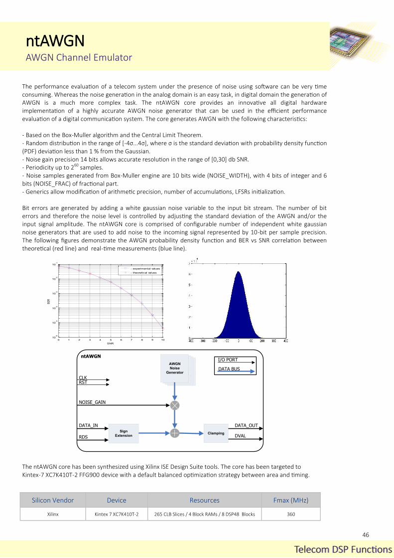
46
ntAWGN AWGN Channel Emulator
Telecom DSP FunctionsTelecom DSP Functions
ntAWGN AWGN Channel Emulator
The performance evaluation of a telecom system under the presence of noise using software can be very time consuming. Whereas the noise generation in the analog domain is an easy task, in digital domain the generation of AWGN is a much more complex task. The ntAWGN core provides an innovative all digital hardware implementation of a highly accurate AWGN noise generator that can be used in the efficient performance evaluation of a digital communication system. The core generates AWGN with the following characteristics: - Based on the Box-Muller algorithm and the Central Limit Theorem. - Random distribution in the range of [-4σ...4σ], where σ is the standard deviation with probability density function (PDF) deviation less than 1 % from the Gaussian. - Noise gain precision 14 bits allows accurate resolution in the range of [0,30] db SNR. - Periodicity up to 260 samples. - Noise samples generated from Box-Muller engine are 10 bits wide (NOISE_WIDTH), with 4 bits of integer and 6 bits (NOISE_FRAC) of fractional part. - Generics allow modification of arithmetic precision, number of accumulations, LFSRs initialization. Bit errors are generated by adding a white gaussian noise variable to the input bit stream. The number of bit errors and therefore the noise level is controlled by adjusting the standard deviation of the AWGN and/or the input signal amplitude. The ntAWGN core is comprised of configurable number of independent white gaussian noise generators that are used to add noise to the incoming signal represented by 10-bit per sample precision. The following figures demonstrate the AWGN probability density function and BER vs SNR correlation between theoretical (red line) and real-time measurements (blue line).
Silicon Vendor Device Resources Fmax (MHz)
Xilinx Kintex 7 XC7K410T-2 265 CLB Slices / 4 Block RAMs / 8 DSP48 Blocks 360
The ntAWGN core has been synthesized using Xilinx ISE Design Suite tools. The core has been targeted to Kintex-7 XC7K410T-2 FFG900 device with a default balanced optimization strategy between area and timing.
0 1 2 3 4 5 6 7 8 9 1010
-6
10-5
10-4
10-3
10-2
10-1
SNR
BE
R
: experimental values
: theoretical values
AWGN
NOISE
GENERATOR
AWGN
NOISE
GENERATOR
I/O PORT
DATA BUS
ntAWGN
AWGN
Noise
Generator
Sign
ExtensionClamping
NOISE_GAIN
DATA_IN
RDS
DATA_OUT
DVAL
CLKRST

47
Telecom DSP FunctionsTelecom DSP Functions
ntSYNC Synchronization Unit
ntSYNC
DINΙ DOUTI
DINQ
DRSRaw Buffer
Coarse
Synchronizer
Raw Metrics
Datapaths
Compensate
Frequency
Offset
Fine
Buffer
Fine
Synchronizer
Preamble
Isolation
Synchronization
Controller
Preamble
Generation
Fine SyncCoarse Sync
OFDM_SIZE
OFDM_NUM
CP
SUBCI
PWR_THRES
DOUTQ
DVAL
SOF
FREQ_OFFS
CLK
CLK2X
Noesis Technologies ntSYNC is a fully programmable component used to achieve time and frequency synchronization in OFDM technology physical layer implementations. It interfaces directly with the physical layer’s front-end (line/RF) interface and using a cross-correlation proprietary algorithm to find the starting point of a received data frame. The generic design approach as well as a number of pre-processed optimizations allow for integration to any OFDM compliant physical layer. The front-end interface feeds the ntSYNC with received signal above a certain power level via the DINI/DINQ ports and flags the signal as valid (DRS). The signal is buffered temporarily in Raw Buffer until raw synchronization phase takes place. The raw synchronization algorithm searches for received power level equal to the a-priori known preamble power levels. The power levels can be programmed via the PWR_THRES input port. Once raw synchronization is achieved the estimated location of the preamble is decided and the coarse synchronization phase begins. Coarse synchronization searches the preamble estimated location more closely with correlative metrics, approximates the received frames starting point and calculates the channels frequency offset shift on the received signal. The raw buffer discards data before the approximated synchronization point and propagates the rest of the signal to the frequency offset compensation unit. The results are being stored in the fine buffer. Additionally the estimated preamble data are being isolated. The isolated preamble is correlated against the known generated preamble by the fine synchronization process. Fine synchronization decides the final synchronization point and discards all previous data in the fine buffer. The programmable OFDM control parameters such as cyclic prefix size (CP), sub-channelization operation (SUBCI), the size of the OFDM symbol (OFDM_SIZE) and the number of OFDM symbols that are expected to be included in the received frame (OFDM_NUM) are required in order to decide the end of the received frame, once the synchronization point has been calculated.
Silicon Vendor Device Resources Fmax (MHz)
Xilinx Kintex 7 XC7K410T-2 5314 CLB Slices / 27 Block RAMs / 96 DSP48 Blocks 86 (CLK) / 102 (CLKX2)
The ntSYNC core has been synthesized using Xilinx ISE Design Suite tools. The core has been targeted to Kintex-7 XC7K410T-2 FFG900 device with a default balanced optimization strategy between area and timing.

48
Noesis Technologies has developed a broad library of channelized E1/T1, E2 & E3 framer/de-framer IP Core solutions that can be used in a variety of time divi-sion multiplexing (TDM) applications including wireless base transceivers, digital subscriber line access multiplexers, voice gateways, private branch exchanges (PBXs), optical network units (ONUs), integrated access devices (IADs), routers and test equipment. The ntE1_G704 and ntT1_G704 cores are fully compliant with Dallas Semiconductor DS2186/DS2187 transmit/receive line interface units. In addition Noesis Technologies, offers the ntHDLC core that implements a single-channel controller for the High-Level Data Link Control (HDLC) protocol that can be used in public networks employing the X.25 communications proto-col, xDSL transport, frame relay and ISDN applications.
Communication Protocols & Networking
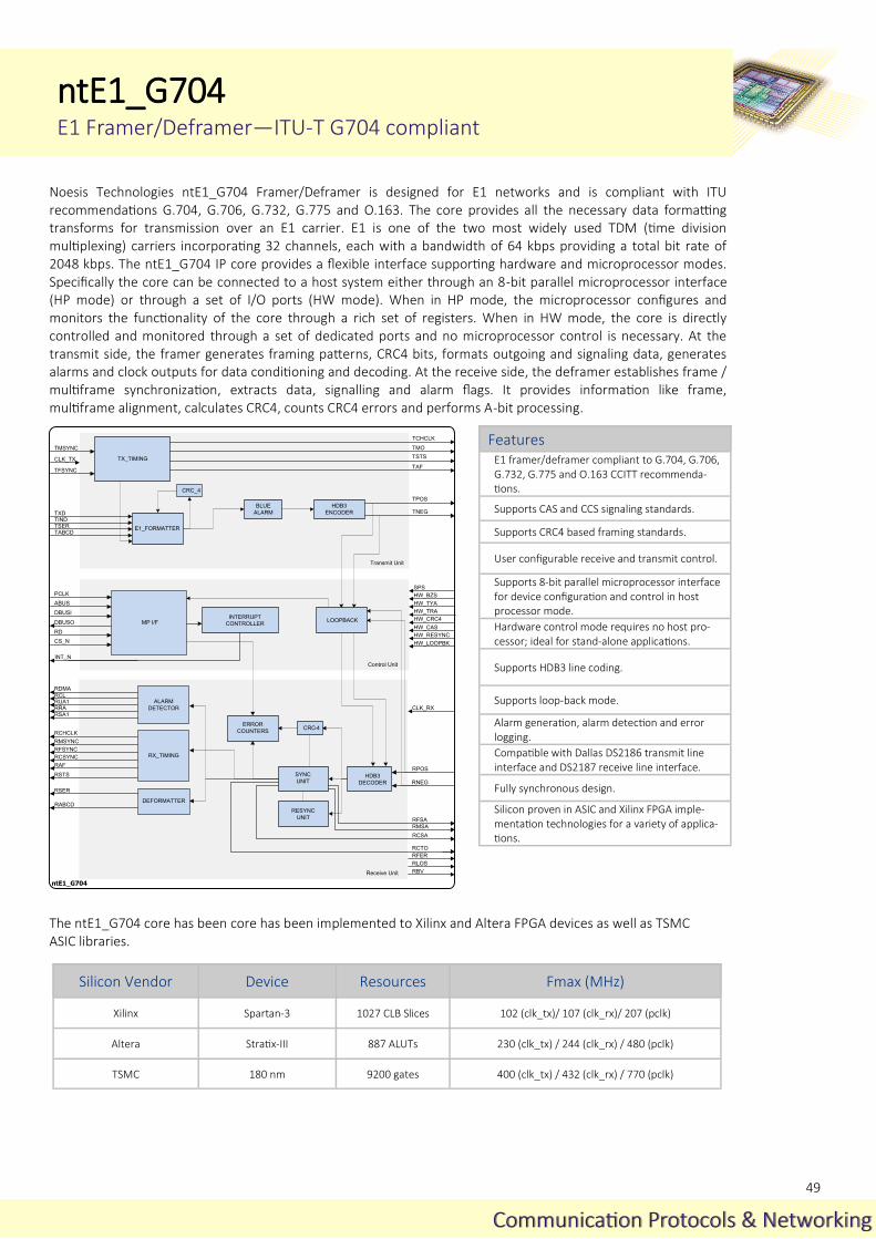
49
Communication Protocols & NetworkingCommunication Protocols & Networking
Noesis Technologies ntE1_G704 Framer/Deframer is designed for E1 networks and is compliant with ITU recommendations G.704, G.706, G.732, G.775 and O.163. The core provides all the necessary data formatting transforms for transmission over an E1 carrier. E1 is one of the two most widely used TDM (time division multiplexing) carriers incorporating 32 channels, each with a bandwidth of 64 kbps providing a total bit rate of 2048 kbps. The ntE1_G704 IP core provides a flexible interface supporting hardware and microprocessor modes. Specifically the core can be connected to a host system either through an 8-bit parallel microprocessor interface (HP mode) or through a set of I/O ports (HW mode). When in HP mode, the microprocessor configures and monitors the functionality of the core through a rich set of registers. When in HW mode, the core is directly controlled and monitored through a set of dedicated ports and no microprocessor control is necessary. At the transmit side, the framer generates framing patterns, CRC4 bits, formats outgoing and signaling data, generates alarms and clock outputs for data conditioning and decoding. At the receive side, the deframer establishes frame / multiframe synchronization, extracts data, signalling and alarm flags. It provides information like frame, multiframe alignment, calculates CRC4, counts CRC4 errors and performs A-bit processing.
ntE1_G704 E1 Framer/Deframer—ITU-T G704 compliant
Features E1 framer/deframer compliant to G.704, G.706, G.732, G.775 and O.163 CCITT recommenda-tions.
Supports CAS and CCS signaling standards.
Supports CRC4 based framing standards.
User configurable receive and transmit control.
Supports 8-bit parallel microprocessor interface for device configuration and control in host processor mode.
Hardware control mode requires no host pro-cessor; ideal for stand-alone applications.
Supports HDB3 line coding.
Supports loop-back mode.
Alarm generation, alarm detection and error logging.
Compatible with Dallas DS2186 transmit line interface and DS2187 receive line interface.
Fully synchronous design.
Silicon proven in ASIC and Xilinx FPGA imple-mentation technologies for a variety of applica-tions.
Silicon Vendor Device Resources Fmax (MHz)
Xilinx Spartan-3 1027 CLB Slices 102 (clk_tx)/ 107 (clk_rx)/ 207 (pclk)
Altera Stratix-III 887 ALUTs 230 (clk_tx) / 244 (clk_rx) / 480 (pclk)
TSMC 180 nm 9200 gates 400 (clk_tx) / 432 (clk_rx) / 770 (pclk)
ABUS
DBUSI
CS_N
RD
TCHCLK
TMO
TSTS
RPOS
TAF
TMSYNC
TFSYNC
CLK_TX
TSER
TXD TIND
TABCD
RMSYNC
RCHCLK
RFSYNC
RSTS
RAF
RSER
RABCD
RDMA
RCL
RCSYNC
Transmit Unit
Control Unit
MP I/FINTERRUPT
CONTROLLERLOOPBACK DBUSO
INT_N
HDB3
ENCODER
E1_FORMATTER
CRC_4
TX_TIMING
TPOS
TNEGBLUE
ALARM
RNEG
CLK_RX
HDB3
DECODER
SYNC
UNIT
RESYNC
UNIT
CRC-4ERROR
COUNTERS
DEFORMATTER
RRA RUA1
RSA1
HW_TYA
HW_BZS
Receive Unit
RFSA
RMSA
RCSA
RCTO
RLOS
RBV
RFER
SPS PCLK
ALARM
DETECTOR
RX_TIMING
HW_TRA
HW_CRC4
HW_CAS
HW_RESYNC
HW_LOOPBK
ntE1_G704
The ntE1_G704 core has been core has been implemented to Xilinx and Altera FPGA devices as well as TSMC ASIC libraries.

50
Communication Protocols & NetworkingCommunication Protocols & Networking
ntT1_G704 T1 Framer/Deframer—ITU-T G704 compliant
Noesis Technologies ntT1_G704 Framer/Deframer is designed for T1 networks and is compliant with ITU recommendations G.704, G.706, G.732, G.775 and O.163. The core provides all the necessary data formatting transforms for transmission over an T1 carrier. T1 is one of the two most widely used TDM (time division multiplexing) carriers incorporating 24 channels, each with a bandwidth of 64 kbps providing a total payload bit rate of 1536 kbps. The ntT1_G704 IP core provides a flexible interface supporting hardware and microprocessor modes. Specifically the core can be connected to a host system either through an 8-bit parallel microprocessor interface (HP mode) or through a set of I/O ports (HW mode). When in HP mode, the microprocessor configures and monitors the functionality of the core through a rich set of registers. When in HW mode, the core is directly controlled and monitored through a set of dedicated ports and no microprocessor control is necessary. At the transmit side, the framer generates framing patterns, CRC6 bits, formats outgoing and signaling data, generates alarms and clock outputs for data conditioning and decoding. At the receive side, the deframer establishes frame / multiframe synchronization, extracts data, signalling and alarm flags. It provides information like frame, multiframe alignment, calculates CRC6 and counts CRC6 errors.
Features T1 framer/deframer compliant to G.704, G.706, G.732, G.775 and O.163 CCITT recommenda-tions.
Supports common framing standards. - 12 frames/superframe ‘193S’ - 24 frames/superframe ‘193E’
Supports CRC6/non-CRC6 cases.
Three zero suppression modes: B7 stuffing, B8ZS and transparent.
User configurable receive and transmit control.
Supports 8-bit parallel microprocessor interface for device configuration and control in host processor mode.
Hardware control mode requires no host pro-cessor; ideal for stand-alone applications.
Supports loop-back mode.
Alarm generation, alarm detection and error logging.
Compatible with Dallas DS2186 transmit line interface and DS2187 receive line interface.
Fully synchronous design.
Silicon proven in ASIC and Xilinx FPGA imple-mentation technologies for a variety of applica-tions.
Silicon Vendor Device Resources Fmax (MHz)
Xilinx Spartan-3 1027 CLB Slices / 12 Block RAMs 101 (clk_tx)/ 100 (clk_rx)
TSMC 180 nm 7050 gates NAND2 equivalent /
4632 RAM bits 432 (clk_tx) / 350 (clk_rx)
The ntT1_G704 core has been core has been implemented in Xilinx FPGA devices as well as in TSMC ASIC libraries.
ABUS
DBUSI
CS_N
RD
TCHCLK
TMO
TSIGSEL
RPOS
TSIGFR
TMSYNC
TFSYNC
CLK_TX
TSER TLINK
TABCD
RMSYNC
RCHCLK
RFSYNC
RSIGFR
RSIGSEL
RSER
RABCD
RCL
RCLK
Transmit Unit
Control Unit
MP I/FINTERRUPT
CONTROLLERLOOPBACK DBUSO
INT_N
B8ZS
ENCODER
T1_FORMATTER
CRC6_GEN
TX_TIMING
TPOS
TNEGBLUE
ALARM
RNEG
CLK_RX
B8ZS
DECODER
SYNC
UNIT
RESYNC
UNIT
CRC6
CHECKERROR
COUNTERS
DEFORMATTER
RYEL RUA1
HW_TYA
HW_BZS
Receive Unit
RFSA
RMSA
RCSA
RCTO
RLOS
RBV
RFER
SPS
ALARM
DETECTOR
RX_TIMING
HW_B7
HW_193E
HW_EXTSI
HW_LOOPBK
ntT1_G704
TSIGFR
TLCLK
RLINK

51
Communication Protocols & NetworkingCommunication Protocols & Networking
ntE2_E3 E2 & E3 Framer/Deframer—ITU-T G742/G751 compliant
Noesis Technologies ntE2_E3 Framer/Deframer is designed for E2/E3 networks and supports all requirements of ITU recommendations G.742, G.751 and G.775. The core provides all the necessary data formatting transforms for transmission over E2/E3 networks. The device can by controlled through a simple set of dedicated ports, allowing robust operation. One ntE2_E3 core instance can operate either as an E1/E2 (2.048/8.448 Mbps) rate Multiplexer/Demultiplexer, or as an E2/E3 (8.448/34.368 Mbps) rate Multiplexer/Demultiplexer. In addition five ntE2_E3 cores can be instantiated to operate as an E1/E3 (2.048/34.368 Mbps) rate Multiplexer/Demultiplexer. The transmit side of the framer generates framing patterns, transmits the alarm and the national bits, interleaves the four tributaries into the high level data stream, calculates the justification mechanism status and the nature of the stuffing bits available, as well as generates alarms, status bits, and clock outputs. The receive side establishes frame synchronization, extracts the interleaved data, the alarm and national bits as well as the auxiliary channels data, monitors for error conditions and generates alarm flags, data valid bits, status bits and clock outputs. The HDB3 codecs can be either used or bypassed, on both transmit and receive sides, depending on the application. Finally both local and remote loopback features are available.
Features
E2/E3 framer/deframer compliant to G.742, G.751, G.775 ITU-T standards.
Performs four E1 to one E2 or four E2 to one E3 multiplexing and vice-versa demultiplexing.
Five ntE2_E3 cascaded cores implement a six-teen E1 to one E3 Multilpexer/Demultilpexer.
Optional HDB3 Line Codecs one both Receive and Transmit sides.
Local and Remote Loop-back modes.
Configurable Frame Alignment Signal.
User access to the Alarm bit and the National bit.
User access to four low speed Auxiliary Chan-nels, one per multiplexed tributary, available via unused Stuffing bits.
Alarm generation, alarm detection and error logging.
Fully synchronous and parametric design.
Silicon proven in ASIC and FPGA technologies for a variety of applications.
Silicon Vendor Device Resources Fmax (MHz) Configuration
Xilinx Virtex-6 436 CLB Slices 170 (clk_tx)/ 250 (clk_rx) E2 mode (2Mbps/8 Mbps)
Xilinx Virtex-6 406 CLB Slices 186 (clk_tx) / 205 (clk_rx) E3 mode (8Mbps/34 Mbps)
The ntE2_E3 core has been core has been implemented in Xilinx FPGA devices.
FIFO
FIFO
FIFO
FIFO
HDB3
Decoder
HDB3
Decoder
HDB3
Decoder
HDB3
Decoder
FORMATTER
Local / Remote
Loopback
DEFORMATTER
TI_SER0
TI_SER1
TI_SER2
TI_SER3
TI_POS0
TI_NEG0
TI_POS1
TI_NEG1
TI_POS2
TI_NEG2
TI_POS3
TI_NEG3
TI_CLK0
TI_CLK1
TI_CLK2
TI_CLK3
CL
K_
TX
RS
T_
N
CE
N_
TX
S_
RS
T
TI_HDB3
TFAIS TFAIS0 TFAIS1 TFAIS2 TFAIS3
TO_RDY
TO_DVAL TO_DATA
TA_MAINT F0_ERR F1_ERR F2_ERR F3_ERR
TO_POS
TO_NEG
TO_SER TO_CLK
TO_HDB3
RO_DVAL0
RO_POS0 RO_NEG0
RO_SER0
RO_DVAL1
RO_POS1
RO_NEG1
RO_SER1
RO_DVAL2
RO_POS2
RO_NEG2
RO_SER2
RO_DVAL3
RO_POS3
RO_NEG3
RO_SER3
AUXO2
AIS NAT
AUXO_DVAL0 AUXO0
AUXO3
AUXO1 AUXO_DVAL1
AUXO_DVAL2
AUXO_DVAL3
DEMUX
SYNC FSM
Controller
HDB3
Encoder
HDB3
Decoder
CLK_RX
RI_POS
RI_NEG
RI_SER
RST_N
CEN_RX
S_RST
RFAIS
RI_HDB3RO_HDB3
FSYNC
FLOS RA_MAINT
FAS_LOCK
DEF_RDI DEF_AIS
T R A N S M I T
R E C E I V E
LLPBKRLPBK
TX0_BVCNT
RX0_BVCNT
ntE2_E3
MUX
Controller /
ALARM GEN.
TX1_BVCNT TX2_BVCNT TX3_BVCNT
HDB3
Encoder
HDB3
Encoder
HDB3
Encoder
HDB3
Encoder
DEMUX
Controller /
ALARM GEN.

52
Communication Protocols & NetworkingCommunication Protocols & Networking
ntHDLC High Level Data Link Controller
Noesis Technologies ntHDLC single channel High-Level Data Link Controller (HDLC) is a full-duplex transceiver with independent transmit and receive units for synchronous framing bit-level HDLC protocol operations. The ntHDLC can handle interframe and delimiting flags, frame check sequence based on CCITT CRC16/CRC32 polynomial, normal or transparent transmission modes, abort generation and detection. The system interface is very flexible and can be adapted towards FIFO, uP, or DMA controllers. The transmit and receive units and their associated control and status logic are independent. This partitioning strategy enables the Tx and Rx units to be instantiated in different place and/or level of the design hierarchy. Each unit (Tx, Rx and back-end interface) has its own clock domain with synchronous clock enable. Communication between the various clock domains is achieved via synchronization logic blocks.
Features
Single port synchronous serial line interface.
Flag/Abort Generation/Detection.
Zero Insertion/Deletion.
Non-octet alignment detection.
CCITT CRC-16 Generation and Checking.
NRZ/NRZI encoding/decoding.
Transparent mode support.
Receive FIFO overrun detection.
Transmit FIFO underrun detection.
Frame status and frame length indicators.
Runt frame detection.
Seperate clocks for Tx and RX interfaces.
Supports flag in interframe-time fill.
8-bit parallel back-end interface.
Fully synchronous design.
Silicon proven in ASIC and Xilinx FPGA imple-mentation technologies for a variety of applica-tions.
Silicon Vendor Device Resources Fmax (MHz)
Xilinx Spartan-3 460 CLB Slices / 10 Block RAMs
80 (tclk)/ 126 (rclk)/ 140 (tsclk)/124 (rsclk)
Xilinx Virtex-5 200 CLB Slices / 10 Block RAMs
130 (tclk)/ 230 (rclk)/ 310 (tsclk)/313 (rsclk)
Altera Stratix-III 600 ALUTs /
10 M9K RAM Blocks 72 (tclk)/ 139 (rclk)/ 184 (tsclk)/133 (rsclk)
TSMC 180 nm 5800 gates NAND2 equivalent /
74 K RAM bits 340 (tclk)/ 400 (rclk)/ 330 (tsclk)/340 (rsclk)
The ntHDLC core has been core has been implemented to Xilinx and Altera FPGA devices as well as TSMC ASIC libraries.
RECEIVELINE
INTERFACE
RECEIVE CONTROLLER
TRANSMIT CONTROLLER
TRANSMITLINE
INTERFACE
TxFIFO
SYSTEMRX & TX
CONTROL AND
STATUSINTERFACE
RXDRXD
RXD_ENRXD_EN
RCLKRCLK
TXDTXD
TXD_ENTXD_EN
TCLKTCLK
RDATA[7:0]RDATA[7:0]
TDATA[7:0]TDATA[7:0]
RDATA_ENRDATA_EN
TDATA_ENTDATA_EN
REOFREOF
ROVFROVF
RIDLERIDLE
RABORTRABORT
RCRCERCRCE
RUNTRUNT
RFRM_LENRFRM_LEN
RxFIFO
TMODETMODEControlControl
StatusStatus
RFLAGRFLAG
TUNDTUND
RFRM_ERRRFRM_ERR
MAX_FRM_LENMAX_FRM_LEN
RSCLKRSCLK
TSCLKTSCLK
RCLK_ENRCLK_EN
TCLK_ENTCLK_EN
RSCLK_ENRSCLK_EN
TSCLK_ENTSCLK_EN
RSYNC
TSYNC
FLUSH_OUTFLUSH_OUT
CRC_MODECRC_MODE
TEOFTEOF
ENC_MODEENC_MODE
ADDRESSADDRESS
ADDR_MODEADDR_MODE
TOVFTOVF
RUNDRUND
RFRM_VALIDRFRM_VALID
STAT_BYTE_CNTSTAT_BYTE_CNT
CMD_BYTE_CNTCMD_BYTE_CNT
RFIFO_FILL_LEVRFIFO_FILL_LEV
TFIFO_FILL_LEVTFIFO_FILL_LEV
TAFULLTAFULL
ntHDLC

53
OFDM transmission technology is spectrally efficient and very robust to harsh wireless channel environments. It is widely applied in wireless communication systems providing high rate transmission capability coupled with high bandwidth efficiency as well as robustness to multi-path fading and multi-path delay. Its frequency selectivity feature allows the users to disable certain OFDM subcarriers to prevent interfering with the others and makes the technology extremely robust against frequency selective fading transmission conditions. Noesis Technologies ntOFDM_BBP is a custom baseband processor, which im-plements the physical layer of an OFDM, time division duplexing (TDD) system. The baseband processor includes both transmission and reception bit-level and symbol-level processing chains including a sophisticated synchronization unit. The host interface is based on AXI-stream protocol. This custom system implements a subset of 802.16d standard functional options/features and is highly configurable via the integrated register-file. An RF interface module is also included, compatible with Analog Devices AD9361 RF transceiver.
Baseband PHYs

54
Baseband PHYsBaseband PHYs
Noesis Technologies ntOFDM_BBP is a custom baseband processor, which implements the physical layer of an OFDM, time division du-plexing (TDD) system. The baseband processor includes both trans-mission and reception bit-level and symbol-level processing chains including a sophisticated synchronization unit. The host interface is based on an AXI4 stream protocol. This high performance OFDM transmission system is fully compliant with 802.16d (WiMAX) stand-ard and is fully configurable via the integrated register file. An RF interface module is also included, compatible with Analog Devices AD9361 RF transceiver. Other RF interfaces can be supported. The Bit-level processing block (BLPB) transmission chain implements the following functional units : randomization, FEC encoding, inter-leaving and symbol mapping. In BLPB reception chain the following operations are implemented: soft symbol demapping, de-interleaving, FEC decoding and de-randomization. The FEC module implements a powerful error correction scheme based on a concatenation of Reed Solomon—Viterbi algorithms.
Tx Buffer
Wimax Tx
BufferWimax Tx
BufferWimax Tx
BufferControl
Register File
SLPB Rx
Transmitter
Receiver
DATA_CLK
P1_DATA(11:0)
RX_FRAME
TX_FRAME
P0_DATA(11:0)
FB_CLK_RF
ENABLETXNRX_RF
RF_PA_EN
RF_LNA_EN
RF_AGC_EN
VDD_GPO_EN
VDDA_1V3_EN
AXI4 STREAM IF
ntOFDM_BBP
RF Interface
(AD9361
specific)
BLPB RxRx Buffer
BLPB Tx SLPB Tx
AXI4 Wrapper /
Controller
- AXI4 stream
interface
- Overall system
synchronization
Synchronizer
Silicon Vendor Device Resources Fmax (MHz)
Xilinx Kintex 7
XC7K410T-2 24763 CLB Slices / 128 Block RAMs /
294 DSP48 Blocks 100
The ntOFDM_BBP core has been synthesized using Xilinx ISE Design Suite tools. The core has been targeted to Kintex-7 XC7K410T-2 FFG900 device with a default balanced optimization strategy between area and timing. The implementation details are shown in the following table.
ntOFDM_BBP Multi-Purpose OFDM Baseband Processor
Features
Customized transmit and receive physical layer chains.
Fully synchronous design enabling high throughput TDD operation.
BLPB and SLPB processing blocks.
Implements a sophisticated synchronization algorithm to efficiently detect and isolate received modulated payload information.
Configurable as either downlink (DL) baseband station or uplink (UL) baseband station.
Configurable data randomization, modulation level and code rate.
Decoding algorithm achieves competitive performance results with the minimum possible test patterns and decoding iterations.
Host interface based on AXI4 stream protocol.
RF interfacing supporting Analog Devices AD9361 RF Transceiver.
Synchronous single clock design.
Silicon proven in ASIC and Xilinx FPGA implementation technologies.
The Symbol-level processing block (SLPB) transmission chain implements the following functional units: OFDM symbol transmitter, IFFT, CP insertion. In reception chain the SLPB module is preceded by the synchronization unit, which is searching for known preamble values in order to locate the start an incoming WiMAX sub-frame. Once the sub-frame is located, frequency offset compensation is applied and received information is propagated down to SLPB reception chain. In SLPB reception chain the following operations take place: CP removal, FFT, OFDM symbol receiver, channel estimation, phase offset compensation and channel equalization.

55
Baseband PHYsBaseband PHYs
ntOFDM_BBP OFDM Baseband Processor
The ntOFDM_BBP advanced DSP algorithms eliminate channel white noise effects as well as frequency and phase offset distortions. BER vs Eb/No performance curves are shown in the figure below for an AWGN channel, for BPSK, QPSK and QAM16 modulation levels as well as for 1/2 and 3/4 coding rates.
The following table presents for various operation modes the achievable throughput rates for 16-sub-channels (full sub-channelization mode), 1/8 cyclic prefix, TDD mode and 50 MHz system clock frequency.
Operation mode Throughput rate (Mbps)
BPSK—Code rate 1/2 12
QPSK—Code rate 1/2 25
QPSK—Code rate 3/4 33
QAM16—Code rate 1/2 31
QAM16—Code rate 3/4 38

56
Baseband PHYsBaseband PHYs
Noesis Technologies ntGhn_BBP is a fully ITU-T G.9960/G.9964 compliant baseband processor, featuring a highly innovative configurable architecture that enables unprecedented power-line throughput rates. It can be used in a variety of applications including smart grid and home automation, high bandwidth home networking, IPTV infrastructure, consumer electronics. The ntGhn_BBP IP core main functional blocks are the transmitter, the receiver, the back-end interface module and the analog front end (AFE) interface. The back-end interface may be optionally wrapped with an AMBA AXI 4 Stream controller. Both the transmitter and the receiver include a local controller and a register file. Via the back-end interface the user may write or read data and configure the cores to operate with a specific functional mode of operation (control profile). The Transmitter PCS component encodes the active register file control information to a Header data block and computes all derivative control configuration parameters required for Payload transmission. As per G.9960 both Header and Payload data blocks are scrambled, LDPC encoded, (optionally) repetition encoded and finally partitioned to Symbol Frames in the PMA component of the Transmitter. The PMD component of the Transmitter modulates and tone maps the symbol frame data segments to OFDM symbols. The OFDM symbols are then processed by the constellation scrambler and the IFFT, which transforms the signal from the frequency to the time domain. The time domain signal is cyclic prefix extended, windowed and finally overlapped to form the final PHY Frame. The formed PHY Frame is provided to the AFE transmit interface, which synchronizes the symbols to the front end clock rate.
ntGhn_BBP Home PLC Baseband Processor (under dev)
Features G.hn physical layer (PHY) baseband processor is compliant to ITU-T G.9960 and ITU-T G.9964 standards
Supports telephone line, power line and coaxial (baseband and RF) bandplans
Supports MSG, ACK, RTS and CTS Frame Types and has infrastructure to easily implement all other G.9960 defined frame types
Highly programmable core supports all standard defined configuration profiles and additionally enables construction of custom configuration profiles
Expandable and highly configurable architecture via a set of generic values with several degrees of parallelism for optimum design approach
Architecture programmability and expandability provide a wide range of trade-offs between core area utilization and information throughput rates
Gb/s information throughput rates can be achieved by expanding the architectural parallelism and selecting high data rate modes of opera-tion in optimum channel conditions, for operating frequency as low as 100MHz
Operating frequency is target technology dependent and raises achieva-ble information throughput proportionally
High speed design approach accomplishes operating frequency greater than 100MHz in medium speed grade FPGA Kintex7 prototyping boards
Distributed control pipelines and flow controller mechanism to achieve minimum component flush out times and “variable on-the-fly” configu-rability
Simple and robust core back end interface enables high throughput data flow
Optional “AMBA AXI 4 Stream” compliant back end interface wrapper
Synchronous clock design
The AFE receive interface passes data from the channel to the Synchronizer unit. The Synchronizer is responsible of sensing the channel conditions and establishing a synchronization point in time, in other words it locates the start of the PHY Frame by searching for the Preamble symbols energy levels. After synchronization the Receiver PMD component removes the effects of windowing and the cyclic prefix, applies the FFT transform to cross the signal back to the frequency domain and thoroughly estimates the channel conditions in terms of phase and frequency offsets. Then the Receiver equalizes and compensates the received OFDM symbols accordingly. Once the Header part of the PHY Frame is identified and equalized, it is being demodulated by the tone demapper and passed to the Receiver PMA component for the optional repetition decoding, LDPC decoding and de-scrambling. A CRC check is performed on the received Header information in the Receiver PCS component and if successful, the Payload reception mode of operation is configured. All derivative control configuration parameters required for payload reception are computed by the Receiver PCS component. Then the Payload OFDM symbols are propagated through the remaining Receiver PMD and PMA components according to the selected control configuration. Finally the decoded Payload data blocks are being returned to the User via the back-end interface.

57
Baseband PHYsBaseband PHYs
The ntG3_BBP is a fully compliant ITU-T G.9903 baseband modem that can be used in a wide range of smart grid applications over power lines, including smart metering and energy management in energy generation and distribution systems, lighting and industrial automation as well as automotive EV charging. The ntG3_BBP IP core main functional blocks are the transmitter, the receiver, the register file, the AHB-Lite wrapper and the analog front end interface. The user accesses the core via the AHB interface to either program the register file or provide payload data to the core. By programming the register file the user sets a specific functional mode of operation, requests the ntG3_BBP to transmit a data or acknowledgement PHY frame or accesses remotely received control information.
Silicon Vendor Device Resources Fmax (MHz)
Xilinx Kintex 7
XC7K410T-2 22996 CLB Slices / 105 BRAMs / 87 DSP48s 81
ntG3_BBP Smart Grid PLC Baseband Processor
Features PLC G3 physical layer (PHY) compliant baseband processor as per ITU-T G.9903 Chapter 7 and ITU-T G.9901 Annex B.
CENELEC-A/B (3-148.5kHz) and FCC (9-490kHz) bandplans support.
Aware of basic MAC layer handshaking primitives.
Data rates from a few kbps up to 290kbps.
On the fly programmable control profile selection.
Compliant with AMBA AHB-Lite protocol.
Synchronous clock design.
Silicon proven in Xilinx FPGA implementation technologies.
The Transmitter encodes the active register file control information to an FCH data block and computes all derivative control config-uration parameters required for payload transmission. As per G.9903 both FCH and Payload data blocks are scrambled, Forward Error Correction (FEC) encoded, interleaved and finally modulated and tone mapped to OFDM symbols. These procedures form the bit level processing part of the Transmitter. After the tone mapper, the symbol level processing part of the transmission takes place. The OFDM symbols are optionally pre-emphasized, the IFFT transform is applied, and then the symbols are circular shifted and extended, windowed and overlapped to a concatenated final PHY Frame. The formed PHY Frame is provided to the AFE transmit interface, which synchronizes the symbols to the front end clock rate. The AFE receive interface passes data from the channel to the Synchronizer unit. The Synchronizer is responsible of sensing the channel conditions and establishing a synchronization point in time, in other words it locates the start of the PHY Frame by searching for the Preamble symbols energy levels. After synchronization the Receiver removes the effects of windowing and the cyclic prefix, applies the FFT transform to cross the signal back to the frequency domain and thoroughly estimates the channel conditions in terms of phase and frequency offsets. Then the Receiver equalizes and compensates the received OFDM symbols accordingly. Once the FCH OFDM part identified and equalized, it is being demodulated by the tone demapper and passed to the
receive bit level processing block for de-interleaving, FEC decoding and de-scrambling. A CRC check is performed on the received FCH information and if successful, the Payload reception mode of operation is configured. All derivative control configuration parameters required for payload reception are computed. Then the Payload OFDM symbols are tone demapped, de-interleaved, FEC decoded and descrambled. Finally the decoded payload is being returned to the User via the AHB-Lite interface. The ntPLC_G3_BBP is able to imple-ment basic coordination handshaking for in-teroperability with the MAC layer via designated fields of the Register File. TXOFF_RXON, BUSY_TX and BUSY_RX status flags are imple-mented.PD-DATA.request,PD-DATA.confirm, PD_ACK.request and PD_ACK.confirm status handshake primitives are supported as per G.9903 7.17.
The ntG3_BBP core has been synthesized using Xilinx ISE Design Suite tools. The core has been targeted to Kintex-7 XC7K410T-2 FFG900 device with a default balanced optimization strategy between area and timing. The implementation details are shown in the following table.
ntG3_BBP
FCH
PAYLOAD TX
ControlProfileVector
UserConfiguration
AHB Lite IF
PHY_TX_FRAME
AFE IF
Transmitter Datapath
Tx BIT LEVEL PROCESSING
BLOCK
Tx SYMBOL LEVEL
PROCESSING BLOCK
BLPB Tx Memory
SLPB Tx Memory
PHY_RX_FRAME
Rx CONTROLLER
REGISTER FILE
Tx CONTROLLER
TX BUFFER
Receiver Datapath
BLPB Rx Memory
SLPB Rx Memory
Rx BIT LEVEL PROCESSING
BLOCK
Rx SYMBOL LEVEL
PROCESSING BLOCK
SYNCHRONIZERBLOCK
SYNCHRONIZER Memory
RECEIVED PAYLOAD
RX BUFFER
58
ntG3_BBP Smart Grid PLC Baseband Processor
Baseband PHYsBaseband PHYs
The ntG3_BBP is a highly programmable core, with numerous possible control configurations combinations of parameters such as : □ Band plan selection | □ Modulation Type and Mode | □ OFDM Symbols number | □ Legacy of Full Interleaver | □ 1 or 2 Reed Solomon codewords | □ Tone Map enabled and disabled sub-bands combinations | □ Tone Mask enabled and disabled tones combinations | □ Transmit gain control options The ntG3_BBP IP Core achieves exceptional error correction performance as illustrated in the following FER vs Es/No graphs and is fully compliant with G3-PLC alliance performance masks (http://www.g3-plc.com/home/ ).

59
IP Customization—System Design—Consulting
Noesis Technologies offers expert ASIC, FPGA and DSP development resources to get your product in the market in time. Our highly skilled engineering team has considerable expertise in modeling, design and efficient implementation of telecom systems based on complex DSP algorithms. A list of our services include the following offerings: ► Telecom systems design feasibility analysis and specifications development. ► System level modeling in Matlab or System C. ► Efficient FPGA implementation and system demo prototyping. ► Customization of our existing IP Cores portfolio in terms of performance, interfacing and functionality. ► IP core development. ► Consulting on communications systems implementation in hardware.
60
Noesis Technologies P.C. Patras Science Park Stadiou Rd, Platani Rion GR-26504 - Patras GREECE Phone: +30 2610 911531 Email: [email protected]
www.noesis-tech.com
Rev. 1.5 Copyright © 2019, Noesis Technologies P.C. ALL RIGHTS RESERVED.


