nMOS Operation Cont.When the gate is at a high voltage:– Positive charge on gate of MOS capacitor– Negative charge attracted to body– Inverts a channel under gate to n-type– Now current can flow through n-type silicon
from source through channel to drain, transistor is ON
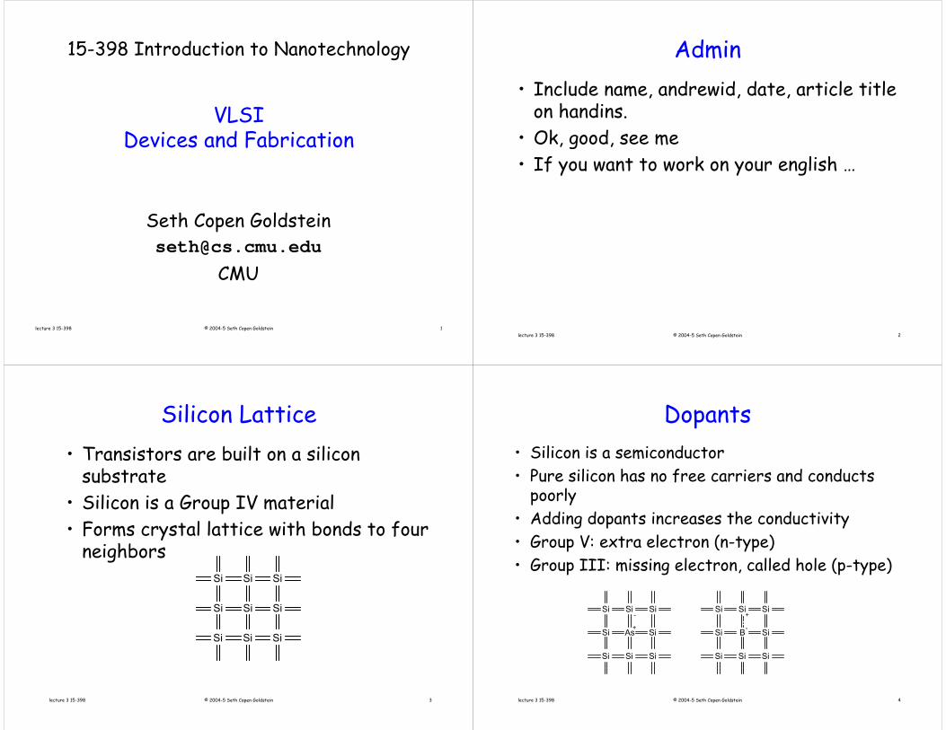
Fabrication Steps• Start with blank wafer• Build inverter from the bottom up• First step will be to form the n-well
– Cover wafer with protective layer of SiO2 (oxide)– Remove layer where n-well should be built– Implant or diffuse n dopants into exposed wafer– Strip off SiO2
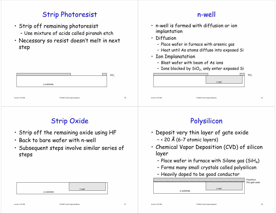
N-diffusion•Pattern oxide and form n+ regions•Self-aligned process where gate blocks diffusion•Polysilicon is better than metal for self-aligned gates because it doesn’t melt during later processing
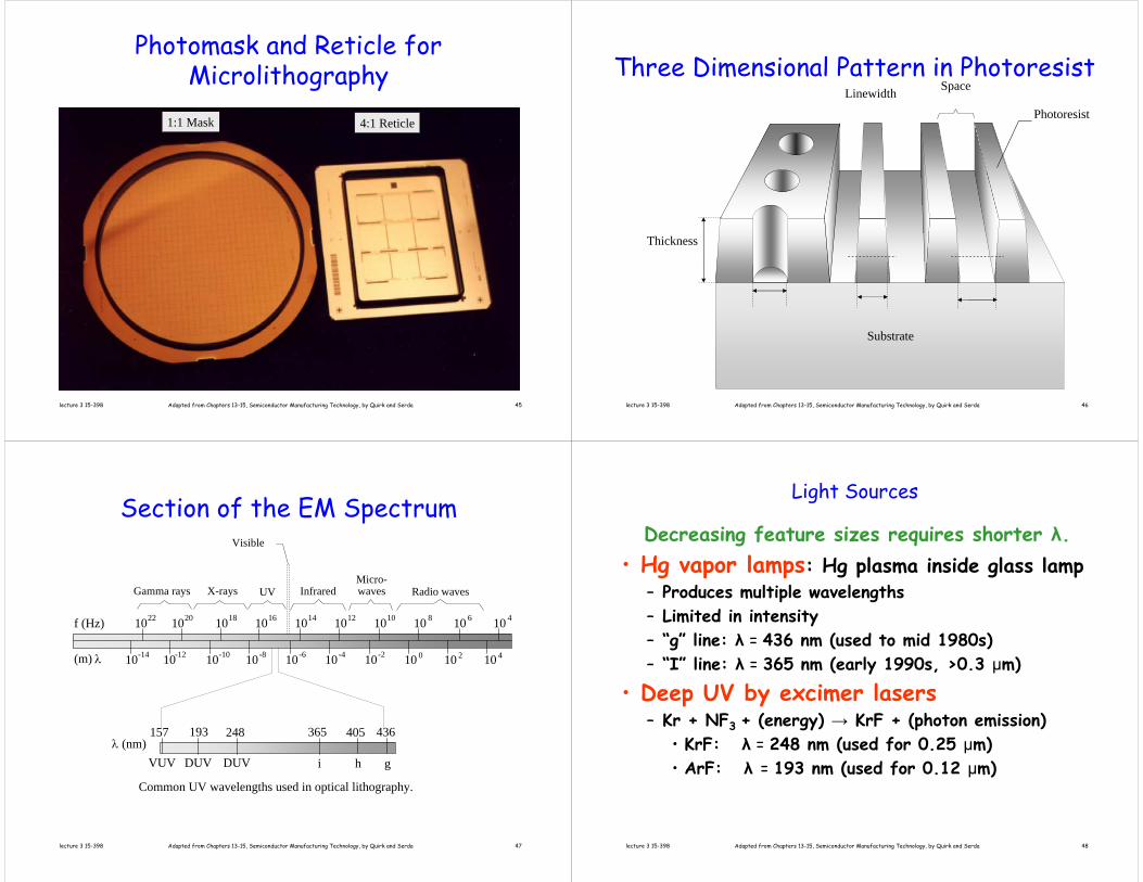
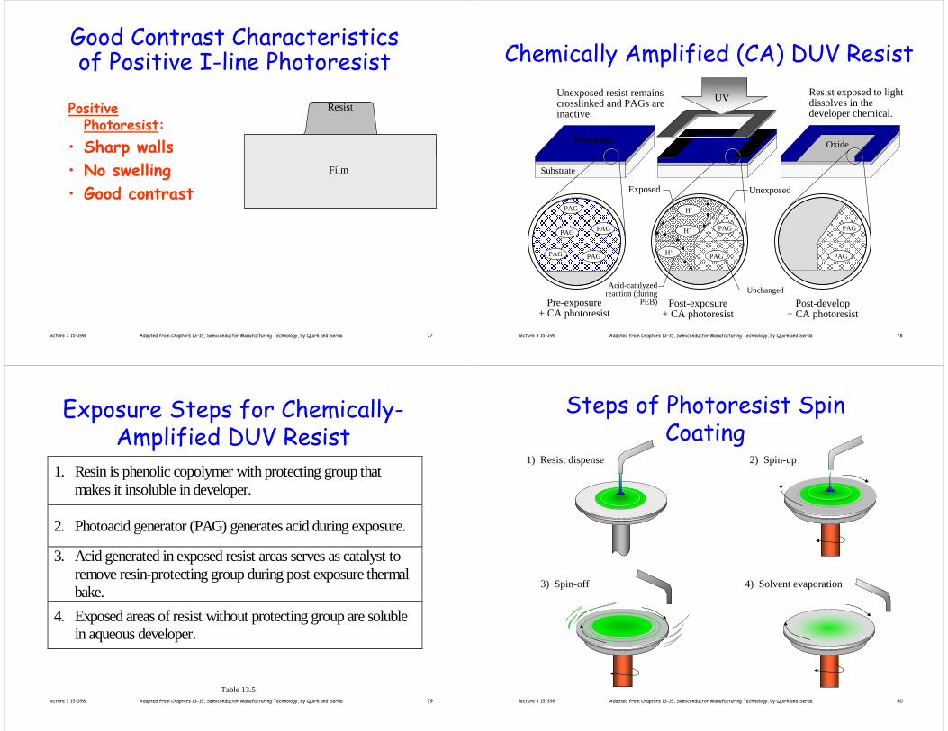
• Deep UV by excimer lasers– Kr + NF3 + (energy) → KrF + (photon emission)
• KrF: λ = 248 nm (used for 0.25 μm)• ArF: λ = 193 nm (used for 0.12 μm)
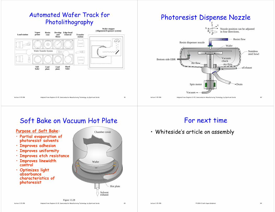
lecture 3 15-398 Adapted from Chapters 13-15, Semiconductor Manufacturing Technology, by Quirk and Serda 49
Important Wavelengths for Photolithography Exposure
UV Wavelength(nm)
WavelengthName UV Emission Source
436 g-line Mercury arc lamp
405 h-line Mercury arc lamp
365 i-line Mercury arc lamp
248 Deep UV (DUV)Mercury arc lamp or
Krypton Fluoride (KrF) excimer laser
193 Deep UV (DUV) Argon Fluoride (ArF) excimer laser
157 Vacuum UV (VUV) Fluorine (F2) excimer laser
Table 13.1
13nm – EUV?
lecture 3 15-398 Adapted from Chapters 13-15, Semiconductor Manufacturing Technology, by Quirk and Serda 50
Importance of Mask Overlay Accuracy
PMOSFET NMOSFET
Cross section of CMOS inverter
Top view of CMOS inverter
The masking layers determine the accuracy by which subsequent processes can be performed.
The photoresist mask pattern prepares individual layers for proper placement, orientation, and size of structures to be etched or implanted.
Small sizes and low tolerances do not provide much room for error.
Figure 13.4
lecture 3 15-398 Adapted from Chapters 13-15, Semiconductor Manufacturing Technology, by Quirk and Serda 51
Mask/Wafer Alignment
Andreou&Wang
• Alignment marks on wafer (from previous pattern) and mask used to align
• Steppers do so automatically•Around 1-5 seconds to align
• Usually marks on left/right of stepped region
lecture 3 15-398 Adapted from Chapters 13-15, Semiconductor Manufacturing Technology, by Quirk and Serda 52
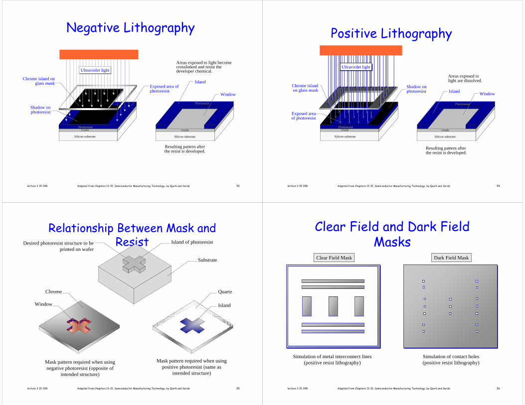
Photolithography Processes
• Negative Resist– Wafer image is opposite of mask image– Exposed resist hardens and is insoluble– Developer removes unexposed resist
• Positive Resist– Mask image is same as wafer image– Exposed resist softens and is soluble– Developer removes exposed resist
lecture 3 15-398 Adapted from Chapters 13-15, Semiconductor Manufacturing Technology, by Quirk and Serda 53
Negative Lithography
Ultraviolet lightUltraviolet light
Island
Areas exposed to light become crosslinked and resist the developer chemical.
Resulting pattern after the resist is developed.
Window
Exposed area of photoresist
Shadow on photoresist
Chrome island on glass mask
Silicon substrateSilicon substrate
PhotoresistPhotoresistOxideOxide
PhotoresistPhotoresist
OxideOxide
Silicon substrateSilicon substrate
lecture 3 15-398 Adapted from Chapters 13-15, Semiconductor Manufacturing Technology, by Quirk and Serda 54
Positive Lithography
photoresist
silicon substrate
oxide oxide
silicon substrate
photoresist
Ultraviolet lightUltraviolet light
Island
Areas exposed to light are dissolved.
Resulting pattern after the resist is developed.
Shadow on photoresist
Exposed area of photoresist
Chrome island on glass mask
Window
Silicon substrateSilicon substrate
PhotoresistPhotoresistOxideOxide
PhotoresistPhotoresist
OxideOxide
Silicon substrateSilicon substrate
lecture 3 15-398 Adapted from Chapters 13-15, Semiconductor Manufacturing Technology, by Quirk and Serda 55
Relationship Between Mask and ResistDesired photoresist structure to be
printed on wafer
Window
Substrate
Island of photoresist
QuartzChrome
Island
Mask pattern required when using negative photoresist (opposite of
intended structure)
Mask pattern required when using positive photoresist (same as
intended structure)
lecture 3 15-398 Adapted from Chapters 13-15, Semiconductor Manufacturing Technology, by Quirk and Serda 56
Clear Field and Dark Field Masks
Simulation of contact holes(positive resist lithography)
Simulation of metal interconnect lines(positive resist lithography)
Clear Field Mask Dark Field Mask
lecture 3 15-398 Adapted from Chapters 13-15, Semiconductor Manufacturing Technology, by Quirk and Serda 57
Eight Steps of Photolithography
8) Develop inspect5) Post-exposure bake
6) Develop 7) Hard bake
UV Light
Mask
λ
λ
4) Alignmentand Exposure
Resist
2) Spin coat 3) Soft bake1) Vapor prime
HMDS
lecture 3 15-398 Adapted from Chapters 13-15, Semiconductor Manufacturing Technology, by Quirk and Serda 58
Photolithography Track System
lecture 3 15-398 Adapted from Chapters 13-15, Semiconductor Manufacturing Technology, by Quirk and Serda 59
Vapor PrimeThe First Step of Photolithography:• Promotes Good Photoresist-to-Wafer
Adhesion• Primes Wafer with Hexamethyldisilazane,
HMDS• Followed by Dehydration Bake• Ensures Wafer Surface is Clean and Dry
lecture 3 15-398 Adapted from Chapters 13-15, Semiconductor Manufacturing Technology, by Quirk and Serda 60
Spin CoatProcess Summary:• Wafer is held onto vacuum
chuck• Dispense ~5ml of photoresist• Slow spin ~ 500 rpm• Ramp up to ~ 3000 to 5000
rpm• Quality measures:
– time– speed– thickness– uniformity– particles and defects
Vacuum chuck
Spindle connected to spin motor
To vacuum pump
Photoresist dispenser
lecture 3 15-398 Adapted from Chapters 13-15, Semiconductor Manufacturing Technology, by Quirk and Serda 61
Soft bake
Characteristics of Soft Bake:• Improves Photoresist-to-Wafer Adhesion• Promotes Resist Uniformity on Wafer• Improves Linewidth Control During Etch• Drives Off Most of Solvent in Photoresist• Typical Bake Temperatures are 90 to 100°C
– For About 30 Seconds– On a Hot Plate– Followed by Cooling Step on Cold Plate
lecture 3 15-398 Adapted from Chapters 13-15, Semiconductor Manufacturing Technology, by Quirk and Serda 62
Alignment and ExposureProcess Summary:• Transfers the mask image to the
resist-coated wafer• Activates photo-sensitive
components of photoresist• Quality measures:
– linewidth resolution– overlay accuracy– particles and defects
UV light source
Mask
Resist
λ
lecture 3 15-398 Adapted from Chapters 13-15, Semiconductor Manufacturing Technology, by Quirk and Serda 63
Post-Exposure Bake
• Required for Deep UV Resists• Typical Temperatures 100 to 110°C on a hot plate
• Immediately after Exposure• Has Become a Virtual Standard for DUV and Standard Resists
lecture 3 15-398 Adapted from Chapters 13-15, Semiconductor Manufacturing Technology, by Quirk and Serda 64
Photoresist DevelopmentProcess Summary:• Soluble areas of
photoresist are dissolved by developer chemical
• Visible patterns appear on wafer- windows- islands
• Quality measures:- line resolution- uniformity- particles and defects
Vacuum chuck
Spindle connected to spin motor
To vacuum pump
Develop dispenser
lecture 3 15-398 Adapted from Chapters 13-15, Semiconductor Manufacturing Technology, by Quirk and Serda 65
Hard Bake• A Post-Development Thermal Bake• Evaporate Remaining Solvent• Improve Resist-to-Wafer Adhesion• Higher Temperature (120 to 140°C) than
Soft Bake
lecture 3 15-398 Adapted from Chapters 13-15, Semiconductor Manufacturing Technology, by Quirk and Serda 66
Develop / Inspect
• Inspect to Verify a Quality Pattern– Identify Quality Problems (Defects)– Characterize the Performance of the Photolithography Process
– Prevents Passing Defects to Other Areas• Etch• Implant
– Rework Mis-processed or Defective Resist-coated Wafers
• Typically an Automated Operation
lecture 3 15-398 Adapted from Chapters 13-15, Semiconductor Manufacturing Technology, by Quirk and Serda 67
Purpose of Photoresist in Wafer Fab• To transfer the mask pattern to the photoresist on the top layer of the wafer surface
• To protect the underlying material during subsequent processing e.g. etch or ion implantation.
lecture 3 15-398 Adapted from Chapters 13-15, Semiconductor Manufacturing Technology, by Quirk and Serda 68
Progressive Improvements in Photoresist
• Better image definition (resolution).• Better adhesion to semiconductor
wafer surfaces.• Better uniformity characteristics.• Increased process latitude (less
sensitivity to process variations).
lecture 3 15-398 Adapted from Chapters 13-15, Semiconductor Manufacturing Technology, by Quirk and Serda 69
• Photoresist– Types of Photoresist– Negative Versus Positive Photoresists


![The Lattice Spacing Variability of Intrinsic Float-Zone Silicon · Measurement Laboratory [MML]). From 1998 to 2011, the NIST lattice comparator played an important role in the International](https://static.documents.pub/doc/80x56/5ac77d887f8b9a40728bedce/the-lattice-spacing-variability-of-intrinsic-float-zone-silicon-laboratory-mml.jpg)


