Silicon microring modulator for 40 Gb/s NRZ-OOK metro networks in O-band
Zhe Xuan,1,* Yangjin Ma,1,2 Yang Liu,2 Ran Ding,2 Yunchu Li,1 Noam Ophir,2 Andy Eu-Jin Lim,3 Guo-Qiang Lo,3 Peter Magill,2 Keren Bergman,4 Tom Baehr-Jones,2 and
Michael Hochberg2,3 1Department of Electrical and Computer Engineering, University of Delaware, Newark, DE, USA
2Coriant Advanced Technology Group, New York, NY, USA 3Institute of Microelectronics, Agency for Science, Technology and Research (A *STAR), Singapore
4Department of Electrical Engineering, Columbia University, New York, NY, USA *[email protected]
Abstract: A microring-based silicon modulator operating at 40 Gb/s near 1310 nm is demonstrated for the first time to our knowledge. NRZ-OOK signals at 40 Gb/s with 6.2 dB extinction ratio are observed by applying a 4.8 Vpp driving voltage and biasing the modulator at 7 dB insertion loss point. The energy efficiency is 115 fJ/bit. The transmission performance of 40 Gb/s NRZ-OOK through 40 km of standard single mode fiber without dispersion compensation is also investigated. We show that the link suffers negligible dispersion penalty. This makes the modulator a potential candidate for metro network applications.
1. Q. Xu, B. Schmidt, S. Pradhan, and M. Lipson, “Micrometre-scale silicon electro-optic modulator,” Nature 435(7040), 325–327 (2005).
2. G. Li, X. Zheng, J. Yao, H. Thacker, I. Shubin, Y. Luo, K. Raj, J. E. Cunningham, and A. V. Krishnamoorthy, “25Gb/s 1V-driving CMOS ring modulator with integrated thermal tuning,” Opt. Express 19(21), 20435–20443 (2011).
3. W. D. Sacher, W. M. J. Green, S. Assefa, T. Barwicz, H. Pan, S. M. Shank, Y. A. Vlasov, and J. K. S. Poon, “Coupling modulation of microrings at rates beyond the linewidth limit,” Opt. Express 21(8), 9722–9733 (2013).
4. W. A. Zortman, A. L. Lentine, D. C. Trotter, and M. R. Watts, “Low-voltage differentially-signaled modulators,” Opt. Express 19(27), 26017–26026 (2011).
5. E. Timurdogan, C. M. Sorace-Agaskar, J. Sun, E. Shah Hosseini, A. Biberman, and M. R. Watts, “An ultralow power athermal silicon modulator,” Nat Commun 5, 4008 (2014).
6. X. Xiao, X. Li, H. Xu, Y. Hu, K. Xiong, Z. Li, T. Chu, J. Yu, and Y. Yu, “44-Gb/s Silicon Microring Modulators Based on Zigzag PN Junctions,” IEEE Photon. Technol. Lett. 24(19), 1712–1714 (2012).
7. Q. Xu, B. Schmidt, J. Shakya, and M. Lipson, “Cascaded silicon micro-ring modulators for WDM optical interconnection,” Opt. Express 14(20), 9431–9435 (2006).
8. Y. Liu, R. Ding, Q. Li, X. Zhe, Y. Li, Y. Yang, A. Lim, P. Lo, K. Bergman, T. Baehr-Jones, and M. Hochberg, “Ultra-compact 320 Gb/s and 160 Gb/s WDM transmitters based on silicon microrings,” in Optical Fiber Communication Conference, OSA Technical Digest (Optical Society of America, 2014), paper Th4G.6.
9. G. P. Agrawal, Fiber-optic Communication Systems, 3rd ed. (Wiley-Interscience, 2002). 10. A. F. Elrefaie, R. E. Wagner, D. A. Atlas, and D. G. Daut, “Chromatic dispersion limitations in coherent
lightwave transmission systems,” J. Lightwave Technol. 6(5), 704–709 (1988). 11. J. P. Turkiewicz and H. De Waardt, “Low complexity up to 400-Gb/s transmission in the 1310-nm wavelength
domain,” IEEE Photon. Technol. Lett. 24(11), 942–944 (2012). 12. M. Streshinsky, R. Ding, Y. Liu, A. Novack, Y. Yang, Y. Ma, X. Tu, E. K. Chee, A. E. Lim, P. G. Lo, T. Baehr-
Jones, and M. Hochberg, “Low power 50 Gb/s silicon traveling wave Mach-Zehnder modulator near 1300 nm,” Opt. Express 21(25), 30350–30357 (2013).
13. F. Y. Gardes, A. Brimont, P. Sanchis, G. Rasigade, D. Marris-Morini, L. O’Faolain, F. Dong, J. M. Fedeli, P. Dumon, L. Vivien, T. F. Krauss, G. T. Reed, and J. Martí, “High-speed modulation of a compact silicon ring resonator based on a reverse-biased pn diode,” Opt. Express 17(24), 21986–21991 (2009).
#215133 - $15.00 USD Received 25 Jul 2014; revised 24 Oct 2014; accepted 29 Oct 2014; published 6 Nov 2014(C) 2014 OSA 17 November 2014 | Vol. 22, No. 23 | DOI:10.1364/OE.22.028284 | OPTICS EXPRESS 28284
14. Y. Liu, R. Ding, M. Gould, T. Baehr-Jones, Y. Yang, Y. Ma, Y. Zhang, A. E.-J. Lim, T. Liow, S. H.-G. Teo, G. Lo, and M. Hochberg, “30GHz silicon platform for photonics system,” in Optical Interconnects Conference, 2013 IEEE, pp. 27–28, IEEE 2013.
15. I.-L. Gheorma and R. M. Osgood, Jr., “Fundamental limitations of optical resonator based high-speed EO modulators,” IEEE Photon. Technol. Lett. 14(6), 795–797 (2002).
16. G. Li, A. V. Krishnamoorthy, I. Shubin, J. Yao, Y. Luo, H. Thacker, X. Zheng, K. Raj, and J. E. Cunningham, “Ring resonator modulators in silicon for interchip photonic links,” IEEE J. Sel. Top. Quantum Electron. 19(6), 3401819 (2013).
17. E. Dulkeith, F. Xia, L. Schares, W. M. Green, and Y. A. Vlasov, “Group index and group velocity dispersion in silicon-on-insulator photonic wires,” Opt. Express 14(9), 3853–3863 (2006).
18. R. Ding, Y. Liu, Q. Li, Z. Xuan, Y. Ma, Y. Yang, A. E.-J. Lim, G.-Q. Lo, K. Bergman, T. Baehr-Jones, and M. Hochberg, “A Compact Low-Power 320-Gb/s WDM Transmitter Based on Silicon Microrings,” IEEE Photonics Journal 6(3), 6600608 (2014).
19. P. Dong, S. Liao, D. Feng, H. Liang, D. Zheng, R. Shafiiha, C. C. Kung, W. Qian, G. Li, X. Zheng, A. V. Krishnamoorthy, and M. Asghari, “Low Vpp, ultralow-energy, compact, high-speed silicon electro-optic modulator,” Opt. Express 17(25), 22484–22490 (2009).
20. G.652: Characteristics of a single-mode optical fibre and cable (11/2009), International Telecommunication Union. Accessed Jun 1st, 2014. https://www.itu.int/rec/T-REC-G.652-200911-I/en
21. B. Ben Bakir, A. V. de Gyves, R. Orobtchouk, P. Lyan, C. Porzier, A. Roman, and J.-M. Fedeli, “Low-Loss (<1 dB) and Polarization-Insensitive Edge Fiber Couplers Fabricated on 200-mm Silicon-on-Insulator Wafers,” IEEE Photon. Technol. Lett. 22(11), 739–741 (2010).
1. Introduction
Silicon photonics offers a promising solution to meet the ever-growing bandwidth requirements of chip-to-chip, data center, and telecom applications. Silicon microring modulators have attracted extensive research interest in recent years [1–4]. The microring modulator is known to exhibit low switching power [5], small footprint, high-speed operation [6], and can easily scale into WDM systems [7, 8]. Conventionally, C-band (centered at 1550 nm) modulators have received the most research attention because of the lower loss, reduced four-wave-mixing effects and longer unrepeated transmission distances in C-band network. However, at 1550 nm standard single mode fibers (SSMF) exhibit strong chromatic dispersion (CD) [9], therefore high data rate (25 Gb/s and higher) direct-detected on-off keying (OOK) transmission is limited to short distance links [10] if not equipped with CD controls. On the other hand, SMF exhibits minimal dispersion in the O-band (centered at 1310 nm), offering the promise of significantly extending the reach without requiring CD compensation. It should be noted that since fiber losses and nonlinear effects are stronger in O-band, they will limit the optical power (particular for WDM systems) and the attainable reach. That being said, a 40 km 8 × 40Gb/s NRZ-OOK WDM system has been demonstrated [11]. We have demonstrated a traveling wave Mach–Zehnder modulator working near 1300nm recently [12].
In this paper, we report the first silicon microring modulator to operate at 40 Gb/s near 1310 nm. The modulator utilizes an asymmetrical p-n junction phase shifter [13] and has a Q-factor of 3,500. Using a 4.8 Vpp driving voltage, the modulator achieves 6.2 dB extinction ratio (ER) at 40 Gb/s with an insertion loss of 7 dB. We transmitted 40 Gb/s NRZ-OOK signal through 40km SSMF with negligible degradation, showing that the device is suitable for high-throughput O-band OOK metro networks. The modulator also has a built-in thermal tuner for future scaling into WDM systems.
#215133 - $15.00 USD Received 25 Jul 2014; revised 24 Oct 2014; accepted 29 Oct 2014; published 6 Nov 2014(C) 2014 OSA 17 November 2014 | Vol. 22, No. 23 | DOI:10.1364/OE.22.028284 | OPTICS EXPRESS 28285
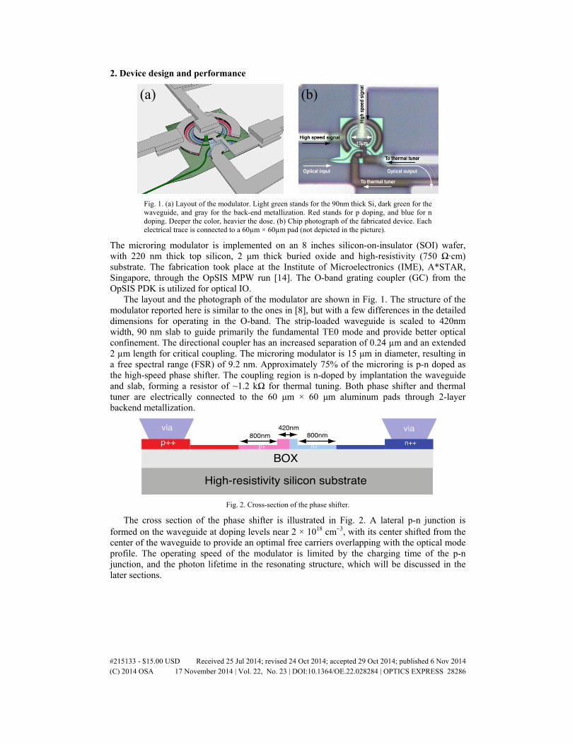
2. Device design and performance
(a) (b)
Fig. 1. (a) Layout of the modulator. Light green stands for the 90nm thick Si, dark green for the waveguide, and gray for the back-end metallization. Red stands for p doping, and blue for n doping. Deeper the color, heavier the dose. (b) Chip photograph of the fabricated device. Each electrical trace is connected to a 60µm × 60µm pad (not depicted in the picture).
The microring modulator is implemented on an 8 inches silicon-on-insulator (SOI) wafer, with 220 nm thick top silicon, 2 μm thick buried oxide and high-resistivity (750 Ω·cm) substrate. The fabrication took place at the Institute of Microelectronics (IME), A*STAR, Singapore, through the OpSIS MPW run [14]. The O-band grating coupler (GC) from the OpSIS PDK is utilized for optical IO.
The layout and the photograph of the modulator are shown in Fig. 1. The structure of the modulator reported here is similar to the ones in [8], but with a few differences in the detailed dimensions for operating in the O-band. The strip-loaded waveguide is scaled to 420nm width, 90 nm slab to guide primarily the fundamental TE0 mode and provide better optical confinement. The directional coupler has an increased separation of 0.24 µm and an extended 2 µm length for critical coupling. The microring modulator is 15 μm in diameter, resulting in a free spectral range (FSR) of 9.2 nm. Approximately 75% of the microring is p-n doped as the high-speed phase shifter. The coupling region is n-doped by implantation the waveguide and slab, forming a resistor of ~1.2 kΩ for thermal tuning. Both phase shifter and thermal tuner are electrically connected to the 60 μm × 60 μm aluminum pads through 2-layer backend metallization.
Fig. 2. Cross-section of the phase shifter.
The cross section of the phase shifter is illustrated in Fig. 2. A lateral p-n junction is formed on the waveguide at doping levels near 2 × 1018 cm−3, with its center shifted from the center of the waveguide to provide an optimal free carriers overlapping with the optical mode profile. The operating speed of the modulator is limited by the charging time of the p-n junction, and the photon lifetime in the resonating structure, which will be discussed in the later sections.
#215133 - $15.00 USD Received 25 Jul 2014; revised 24 Oct 2014; accepted 29 Oct 2014; published 6 Nov 2014(C) 2014 OSA 17 November 2014 | Vol. 22, No. 23 | DOI:10.1364/OE.22.028284 | OPTICS EXPRESS 28286
Fig. 3. (a) Transmission spectrum of the modulator. (b) Enlarged transmission spectra with 0V – (−4)V junction bias voltages. (c) Fitted notch wavelength shift versus junction bias. (d) Enlarged transmission spectra with 0 V – 3 V thermal tuning voltages. The current for each voltage is as follows: 0mA, 0.89 mA, 1.24 mA, 1.49 mA, 1.68 mA, and 1.82 mA. (e) Fitted notch wavelength shift versus thermal power.
Polarization maintaining fiber (PMF) is epoxy attached onto the silicon chip for stable optical coupling throughout the test. The modulator has 25 dB extinction ratio (ER) and ~2 dB on-chip loss, as shown in Fig. 3(a). The on-chip propagation loss is ~1 dB, and the insertion loss of the modulator is ~1 dB, which is caused by the single-pass loss of the microring resonator, i.e., the scattering and absorption loss from the doped coupling region. The full width at half maximum (FWHM) near 1314 nm is 0.372 nm (65GHz), corresponding to a Q-factor is ~3,500. The optical modulation bandwidth can be calculated as
12
12(2 1) 42optf FWHM GHz= − × = [15]. By applying different reverse biases to the p-n
junction, the junction tunability is measured to be 14.2 pm/V, as shown in Fig. 3(b) and 3(c). The corresponding VπL of the phase shifter is 2.2 V-cm. The thermal tuning response is characterized by injecting electrical power into the resistor mentioned above. The fitted tuning efficiency is 0.2 nm/mW (i.e., 46 mW per FSR), as shown in Fig. 3(d) and 3(e).
0 10 20 30−40
−30
−20
−10
0
10
S11
Phas
e [d
egre
e]
0 10 20 30−4
−3
−2
−1
0
1
Frequency [GHz]
S11
Mag
nitu
de [d
B]
(a) (b)
Cpad6fF
Cj30fFRs
70Ω Z0
50Ω
Source
Fig. 4. (a) RC circuit model at 0V junction bias. Cpad: pad capacitance. Cj: pn junction capacitance. Rs: series resistance from the pad to the junction. (b) Measured S11 (dot) and stimulated S11 of the fitted circuit model (solid).
The electrical portion of the modulator can be modeled as a one-port RC circuit [2]. As shown in Fig. 4(a), the circuit model consists of the pad capacitance Cpad, the p-n junction
#215133 - $15.00 USD Received 25 Jul 2014; revised 24 Oct 2014; accepted 29 Oct 2014; published 6 Nov 2014(C) 2014 OSA 17 November 2014 | Vol. 22, No. 23 | DOI:10.1364/OE.22.028284 | OPTICS EXPRESS 28287
capacitance Cj, and the series resistance Rs from the pad to the junction. Parasitics relating to high-resistivity substrate and thick buried oxide layer are estimated insignificant and are not considered here. By fitting the model to measure the reflection coefficient (S11) at 0V bias, the extracted Cpad, Cj, Rs are 6 fF, 30 fF, 70 Ω, as shown in Fig. 4(b). Taking into account the 50 Ω impedance of a RF source, the RC bandwidth RCf is 43 GHz. Combining with the
optical modulation bandwidth, the overall modulation bandwidth is
12
303
2 2
f fopt RC
f GHzdB
f fopt RC
×= = +
[16], sufficient to support 40 Gb/s operation.
3. 40 Gb/s, 40 km O-band OOK link
If the modulator were used in a high-speed link, both on-chip waveguides and fiber would, in principle, contribute to the dispersion. However, compared to a few millimeter in length waveguide, the dispersion due to the 40 km fiber dominates the loss [17]. The dispersion characteristics of the fiber spool used in the later section (40 km SSMF) is estimated as follows.
Driver
4.8Vpp
Rx Supply
Digital Serial Analyzer
Optical Path
Electrical Path
CW Laser6dBm
PDFALiNbO3
10Gb/s ··· 0101 ···
40km SSMF
1300 1305 1310 1315 1320 1325−1
−0.5
0
0.5
1
Wavelength [nm]
D [p
s/(n
m×k
m)]
0
3.75
7.5
11.25
15
x 10−7
grou
p_in
dex
1300 1305 1310 1315 1320 13250
50
100
150
200
Wavelength [nm]
Rel
ativ
e de
lay
time[
ps]
(a) (b)
(c) (d)
Fig. 5. (a) Fiber dispersion characterization setup. PDFA: praseodymium-doped fiber amplifier. LiNbO3: commercial LiNbO3-based Mach-Zehnder modulator. Rx: receiver. (b) The measured waveform as seen on oscilloscope at different wavelengths. The red arrows indicate the time stamp of the rising edge. (c) Relative delay time versus the wavelength. Dot: measured data points. Curve: spline interpolation. The corresponding group index difference is annotated on the right Y-axis. (d) Calculated dispersion curve.
The test setup used to characterize the fiber dispersion is illustrated in Fig. 5(a). A tunable CW laser output at 6 dBm is modulated by 10 Gb/s NRZ repeated 0101 sequence through a commercial LiNbO3 modulator. The modulated optical signal is amplified by a praseodymium-doped fiber amplifier (PDFA), transmitted through 40 km fiber, and then picked up by a high-speed receiver of −10 dBm Pavg sensitivity. By varying the laser wavelength, i.e., the group velocity through the fiber, the delay time would be different, and the detected waveform would shift back and forth on the digital serial analyzer (DSA), which is illustrated in Fig. 5(b). The relation between delay time and the wavelength is established by tracking the time stamp of rising edges, as indicated by arrows in Fig. 5(b), and is further
#215133 - $15.00 USD Received 25 Jul 2014; revised 24 Oct 2014; accepted 29 Oct 2014; published 6 Nov 2014(C) 2014 OSA 17 November 2014 | Vol. 22, No. 23 | DOI:10.1364/OE.22.028284 | OPTICS EXPRESS 28288
converted into group index (Ng) difference, as shown in Fig. 5(c). The fiber has a group delay minima, i.e. a zero-dispersion wavelength (λ0), between 1310 nm and 1315 nm. The fiber
dispersion coefficient can be approximated by gNDλ λ
Δ=
Δ, as shown in Fig. 5(d). The λ0 is
estimated to be 1312.5 nm from the figure.
Rx Supply
Digital Serial Analyzer
Optical Path
Electrical Path
CW Laser6dBm
SOA PDFA
4:1 MUX
4 x 10Gb/s PRBS31
Driver
4.8Vpp
MOD
0 / 20km / 40km SSMF
Filter
DC Source
(a)
(b) (c)
Fig. 6. (a) High-speed data link testbench. MOD: microring modulator. Rx: receiver. SOA: semiconductor optical amplifier. (b) Layout of the filter. (c) Chip photograph of the fabricated device.
We then set up a 40 Gb/s O-band OOK link with the microring modulator and SSMF discussed above. The data link is sketched in Fig. 6(a). The tunable CW laser output is modulated by the microring modulator. The 40 Gb/s test pattern is generated from 4 × 10 Gb/s PRBS31 pulse pattern generators (PPG) and a 4:1 multiplexer (MUX). The pattern is then amplified to 4.8 Vpp and drives the microring modulator through a bias-tee and a special RF probe. The probe has 50 Ω shunt resistor at the tips to suppress the back-reflection, which could damage the driver amplifier (It is worth noting that, in this special case, due to the additional resistor loaded by the modulator, the aforementioned RC bandwidth RCf is no
longer 43GHz. The actual bandwidth will depend on the additional resistor and its parasitics). To overcome the large coupling loss, the 40 Gb/s link employs an additional optical amplification stage, a semiconductor optical amplifier (SOA) followed by a tunable silicon microring filter. The silicon microring filter is implemented in the same process, and 50% of the microring is n-doped as a 1.5 kΩ thermal tuner, as shown in Fig. 6(b) and 6(c). It has 9.3 nm FSR and 0.997 nm (174 GHz) FWHM at drop port, sufficient to pass 40 Gb/s signal while stopping the out-of-band ASE noise from the SOA. The thermal tunability is measured to be 0.24 nm/mW (i.e., 39 mW per FSR). The SOA’s output is, at first, fed into an optical sampling module during the initialization process of the microring modulator.
In the measurement, the wavelength is initially set to a −6 dB insertion loss point [18] near λ0. The junction bias and laser wavelength are then optimized to achieve the best ER with decent eye diagram symmetry. The optimized junction bias and wavelength is −2.6 V and 1314.852 nm. The insertion loss is −7 dB. The optical eye diagram with 6.2 dB ER is shown in Fig. 7(a). Combined with the measured Cj of 20 fF near −2.6 V bias, the dynamic energy consumption of the modulator can be calculated to be 115 fJ/bit using CjVpp
2/4 [19]. The
#215133 - $15.00 USD Received 25 Jul 2014; revised 24 Oct 2014; accepted 29 Oct 2014; published 6 Nov 2014(C) 2014 OSA 17 November 2014 | Vol. 22, No. 23 | DOI:10.1364/OE.22.028284 | OPTICS EXPRESS 28289
SOA’s output is then fed into the filter, and the drop port is thermally aligned to the previous optimized wavelength by measuring its optical power with a power meter. The filtered signal is amplified by the PDFA and propagates through 0 km, 20 km and 40 km SSMF to the receiver. The PDFA is adjusted to maintain roughly a −3.8 dBm Pavg into the receiver. Measured electrical eye diagrams are shown in Fig. 7(b)-7(d). The 40 Gb/s bit-stream is transmitted through 20 km and 40 km fiber with 1.2 ps and 2.8 ps jitter degradation, as compared to the back-to-back transmission (0km).
(a) (b)
(c) (d)
Fig. 7. (a) 40 Gb/s optical eye of the modulated signal. Junction bias: −2.6 V. (b)-(d) 40 Gb/s electrical eye after 0km/20km/40km transmission. The average optical power into the receiver is kept at −3.8 dBm by adjusting the PDFA. CW laser wavelength: 1314.852 nm.
Such small jitter degradation can be explained as followed: The laser is operated at 1314.852 nm, 2.3 nm away from λ0. By approximating the signal spectrum width to 80 GHz (0.46 nm), to the first order of approximation, the CD through 40 km SSMF can be estimated as 0.46 nm × 40 km × Dλ = 3.7 ps, where Dλ(λ = 1315 nm) = 0.2 ps/(nm × km) is read from Fig. 5(d). In a general case, since the FSR is 9.2 nm, one can always find an operating wavelength no more than 4.6 nm (FSR/2) from λ0, independent of the specific SSMF used. That implies an upper CD limit of 0.46 nm × 40 km × 4.6 nm × S0max = 7.8 ps, where S0max = 0.092 ps/(nm2 × km) for ITU-T G.652 complaint fibers [20]. The 7.8 ps CD is tolerable for 40 Gb/s bit-stream. In addition, the thermal tuner can be employed to shift the resonance frequencies towards λ0 at an efficiency of 0.2 nm/mW. By applying the proper tuning power and operating at λ0, the CD can be reduced.
One remaining question is the total link budget. While the link presented above has ~52 dB total loss (including 24 dB from four grating couplers) and utilizes two-stage optical amplification, it can be reduced to 27 dB by using low-loss edge coupler [21] (2 dB from two edge couplers, 2 dB on-chip loss, 7 dB bias loss of the modulator, and 16 dB from 40 km fiber). It can well fit into links with 6dBm laser input, −10 dBm receiver sensitivity and a moderate optical amplification (>11dB).
5. Conclusion
We report an O-band modulator based on silicon microring devices. The modulator operates at 40 Gb/s and achieves 6.2 dB ER under 4.8 Vpp drive and 7 dB insertion loss. 40 Gb/s NRZ-
#215133 - $15.00 USD Received 25 Jul 2014; revised 24 Oct 2014; accepted 29 Oct 2014; published 6 Nov 2014(C) 2014 OSA 17 November 2014 | Vol. 22, No. 23 | DOI:10.1364/OE.22.028284 | OPTICS EXPRESS 28290
OOK transmission is demonstrated through 40 km SSMF with minimal degradation, making the modulator suitable for high-throughput short-haul O-band OOK links.
Acknowledgments
The authors thank Qi Li from Columbia University, Andrew Wright and Jian Bai from University of Delaware for the helpful discussions. The authors acknowledge the loan of critical equipment from AT&T, and gratefully acknowledge the support from Portage Bay Photonics. The authors gratefully acknowledge support for the OpSIS initiative from Gernot Pomrenke, of AFOSR. The authors also thank Akira TSUCHIYA for the GDSII importer plugin.
#215133 - $15.00 USD Received 25 Jul 2014; revised 24 Oct 2014; accepted 29 Oct 2014; published 6 Nov 2014(C) 2014 OSA 17 November 2014 | Vol. 22, No. 23 | DOI:10.1364/OE.22.028284 | OPTICS EXPRESS 28291


![RF - AdvanIDe...Data rate = F RF /16 0 01 NRZ data stream Manchester coded RF field Manchester coded Modulator signal 4 4681C–RFID–09/05 ATA5558 [Preliminary] Figure 2-2. Bi-phase](https://static.documents.pub/doc/80x56/60fea832d961fb4d750fd53a/rf-advanide-data-rate-f-rf-16-0-01-nrz-data-stream-manchester-coded-rf.jpg)


