Silicon nanopillar anodes for lithium-ion batteries using nanoimprint lithography with flexible molds Eric Mills, John Cannarella, Qi Zhang, Shoham Bhadra, Craig B. Arnold, and Stephen Y. Chou Citation: Journal of Vacuum Science & Technology B 32, 06FG10 (2014); doi: 10.1116/1.4901878 View online: http://dx.doi.org/10.1116/1.4901878 View Table of Contents: http://scitation.aip.org/content/avs/journal/jvstb/32/6?ver=pdfcov Published by the AVS: Science & Technology of Materials, Interfaces, and Processing Articles you may be interested in In situ cycling and mechanical testing of silicon nanowire anodes for lithium-ion battery applications Appl. Phys. Lett. 100, 243901 (2012); 10.1063/1.4729145 Fabrication of silicon template with smooth tapered sidewall for nanoimprint lithography J. Vac. Sci. Technol. B 29, 06FC16 (2011); 10.1116/1.3662094 High aspect ratio fine pattern transfer using a novel mold by nanoimprint lithography J. Vac. Sci. Technol. B 29, 06FC15 (2011); 10.1116/1.3662080 Sub- 200 nm gap electrodes by soft UV nanoimprint lithography using polydimethylsiloxane mold without external pressure J. Vac. Sci. Technol. B 28, 82 (2010); 10.1116/1.3273535 Silicon nanowires for rechargeable lithium-ion battery anodes Appl. Phys. Lett. 93, 033105 (2008); 10.1063/1.2929373 Redistribution subject to AVS license or copyright; see http://scitation.aip.org/termsconditions. Download to IP: 128.112.142.131 On: Tue, 30 Dec 2014 22:19:15
Transcript
Silicon nanopillar anodes for lithium-ion batteries using nanoimprint lithography withflexible moldsEric Mills, John Cannarella, Qi Zhang, Shoham Bhadra, Craig B. Arnold, and Stephen Y. Chou Citation: Journal of Vacuum Science & Technology B 32, 06FG10 (2014); doi: 10.1116/1.4901878 View online: http://dx.doi.org/10.1116/1.4901878 View Table of Contents: http://scitation.aip.org/content/avs/journal/jvstb/32/6?ver=pdfcov Published by the AVS: Science & Technology of Materials, Interfaces, and Processing Articles you may be interested in In situ cycling and mechanical testing of silicon nanowire anodes for lithium-ion battery applications Appl. Phys. Lett. 100, 243901 (2012); 10.1063/1.4729145 Fabrication of silicon template with smooth tapered sidewall for nanoimprint lithography J. Vac. Sci. Technol. B 29, 06FC16 (2011); 10.1116/1.3662094 High aspect ratio fine pattern transfer using a novel mold by nanoimprint lithography J. Vac. Sci. Technol. B 29, 06FC15 (2011); 10.1116/1.3662080 Sub- 200 nm gap electrodes by soft UV nanoimprint lithography using polydimethylsiloxane mold without externalpressure J. Vac. Sci. Technol. B 28, 82 (2010); 10.1116/1.3273535 Silicon nanowires for rechargeable lithium-ion battery anodes Appl. Phys. Lett. 93, 033105 (2008); 10.1063/1.2929373
Redistribution subject to AVS license or copyright; see http://scitation.aip.org/termsconditions. Download to IP: 128.112.142.131 On: Tue, 30 Dec 2014 22:19:15
Silicon nanopillar anodes for lithium-ion batteries using nanoimprintlithography with flexible molds
Eric MillsNanoStructure Laboratory, Department of Electrical Engineering, Princeton University, Princeton,New Jersey 08544
John CannarellaDepartment of Mechanical and Aerospace Engineering, Princeton University, Princeton, New Jersey 08544
Qi ZhangNanoStructure Laboratory, Department of Electrical Engineering, Princeton University, Princeton,New Jersey 08544
Shoham Bhadra and Craig B. ArnoldDepartment of Mechanical and Aerospace Engineering, Princeton University, Princeton, New Jersey 08544
Stephen Y. Choua)
NanoStructure Laboratory, Department of Electrical Engineering, Princeton University, Princeton,New Jersey 08544
(Received 5 September 2014; accepted 4 November 2014; published 19 November 2014)
The lithium ion battery, a preferred energy storage technology, is limited by its volumetric and
gravimetric energy densities, as well as its capacity retention with prolonged cycling. In this work,
the authors exploited the extremely high lithium storage capacity of Si as an anode material and
tackled the issue of lithium-induced volume expansion by patterning the Si into a nanopillar array
using nanoimprint lithography and reactive-ion etching. Arrays of 200 nm-pitch Si pillars of
50–70 nm diameter and 200–500 nm height were fabricated on stainless steel substrates, assembled
into coin cells, and tested against lithium counter electrodes. Initial charge capacities in excess of
3000 mAh/g, and a low rate-dependence, were obtained with these Si pillar anodes. This represents
an improvement over previously reported nanoimprint-patterned Si anodes. Though this initial
capacity is roughly equivalent to previously reported values for bulk Si anodes, our nanopillar ano-
des exhibit far superior capacity retention with subsequent charge–discharge cycles. VC 2014American Vacuum Society. [http://dx.doi.org/10.1116/1.4901878]
I. INTRODUCTION
The lithium ion battery has become the energy storage me-
dium of choice for almost all applications requiring recharge-
able batteries, due to its favorable performance characteristics
relative to other rechargeable battery chemistries.1,2 However,
for applications with size and weight constraints, such as elec-
tric vehicles, it is still necessary to achieve significant
increases in energy density. Consequently, the development of
battery electrode materials with higher lithium storage capaci-
ties has remained an area of intense research. One promising
anode material is silicon, which shows theoretical Li-storage
specific charge capacities of �3600 mAh/g (Ref. 3) at room
temperature, nearly 10� that of current commercial anodes,
which are typically graphite (372 mAh/g).4 Si anodes made
from �45 lm-sized powders have shown initial capacities of
nearly 4000 mAh/g,5 though anodes made from such “bulk”
Si typically lose 80%–90% of their capacities with 5 cycles.6
This rapid degradation is due to the 310% volume expansion7
that occurs during lithiation, resulting in rapid capacity losses
due to mechanical pulverization of the electrode.
To prevent Si pulverization, it has been widely accepted
that Si electrodes must be nanostructured, as Si systems ex-
hibit a critical “cracking radius,”8 above which structural
integrity is compromised during battery cycling. For the pop-
ular Si nanowire-based anode, first demonstrated by Cui
et al. in 2008,9 this critical radius has been shown to be on
the order of 300 nm for initially crystalline Si.8 Randomly
packed nanowire systems are also popular because they do
not require binders or conductive additives (which reduce
energy density), and they have intrinsic free space to accom-
modate volumetric expansion of the Si electrode material
during lithiation. The accommodation of volumetric expan-
sion is critical for reducing mechanical stress in the individ-
ual structures as well as stress within the cell as a whole,
which can lead to overall cell degradation.10 A number of
deposition-based methods have been used to create viable
Si Nanowire (NW) anodes, including thin film deposition,11
creation of random wire networks,12 and coating existing
fibers with Si via chemical vapor deposition (CVD).13
Etching-based fabrication techniques, involving chemical
etching14 or deep reactive ion etching,15 have also been
implemented, often in combination with self-assembled col-
loidal monolayers to create patterns.14 Random nanowire net-
works, such as those grown by CVD, typically show NWs
growing in many directions12,16 and are thus extremely ineffi-
cient at filling volume. To efficiently fill volume, NWs with
well-defined diameter, pitch, and orientation are required.
Nanoimprint lithography (NIL), in combination with
appropriate deposition and etching techniques, is an ideala)Electronic mail: [email protected]
06FG10-1 J. Vac. Sci. Technol. B 32(6), Nov/Dec 2014 2166-2746/2014/32(6)/06FG10/5/$30.00 VC 2014 American Vacuum Society 06FG10-1
Redistribution subject to AVS license or copyright; see http://scitation.aip.org/termsconditions. Download to IP: 128.112.142.131 On: Tue, 30 Dec 2014 22:19:15
Redistribution subject to AVS license or copyright; see http://scitation.aip.org/termsconditions. Download to IP: 128.112.142.131 On: Tue, 30 Dec 2014 22:19:15
were determined by normalizing the measured capacity
(mAh) by the estimated mass of Si (g) on the electrode. This
was found by estimating the average pillar volume from
SEM images, multiplying by feature density (#/cm2) and an-
ode size (cm2), and converting to mass (2.33 g/cm3). The pil-
lars exhibited deviation in shape from ideal cylinders, so the
reported radius corresponds to that of a cylinder having
equivalent volume and height to the imaged pillars. The
mass loadings are assumed to be uniform among all electro-
des of a given pillar size, and any nonuniformities would
translate to uncertainty in specific capacity.
The capacity-normalized charging rate (C-rate) was deter-
mined by dividing the charging current (mA) by the full the-
oretical capacity of the Si on each wafer, calculated based on
the estimated mass loading (g), and the theoretical specific
charge capacity (3579 mAh/g). Our “1 C” charging rate is
thus equivalent to 3579 mA/g Si, and our “2 C” rate is equiv-
alent to 7158 mA/g Si. All cells were cycled using a CCCV
methodology as follows. The Si is lithiated with a constant
current until the cell voltage decreases to 10 mV. After
reaching 10 mV, the cell is held at 10 mV for 2 h to ensure
complete lithiation of the Si. The 10 mV cut off is chosen to
prevent the undesirable onset of lithium plating on the Si sur-
face, which occurs below 0 V. The Si is subsequently delithi-
ated at a constant current until the cell voltage rises to 1.3 V,
marking the completion of a single cycle. For alternating-
rate experiments, charging current was switched every 3
cycles, between three different values.
III. RESULTS AND DISCUSSION
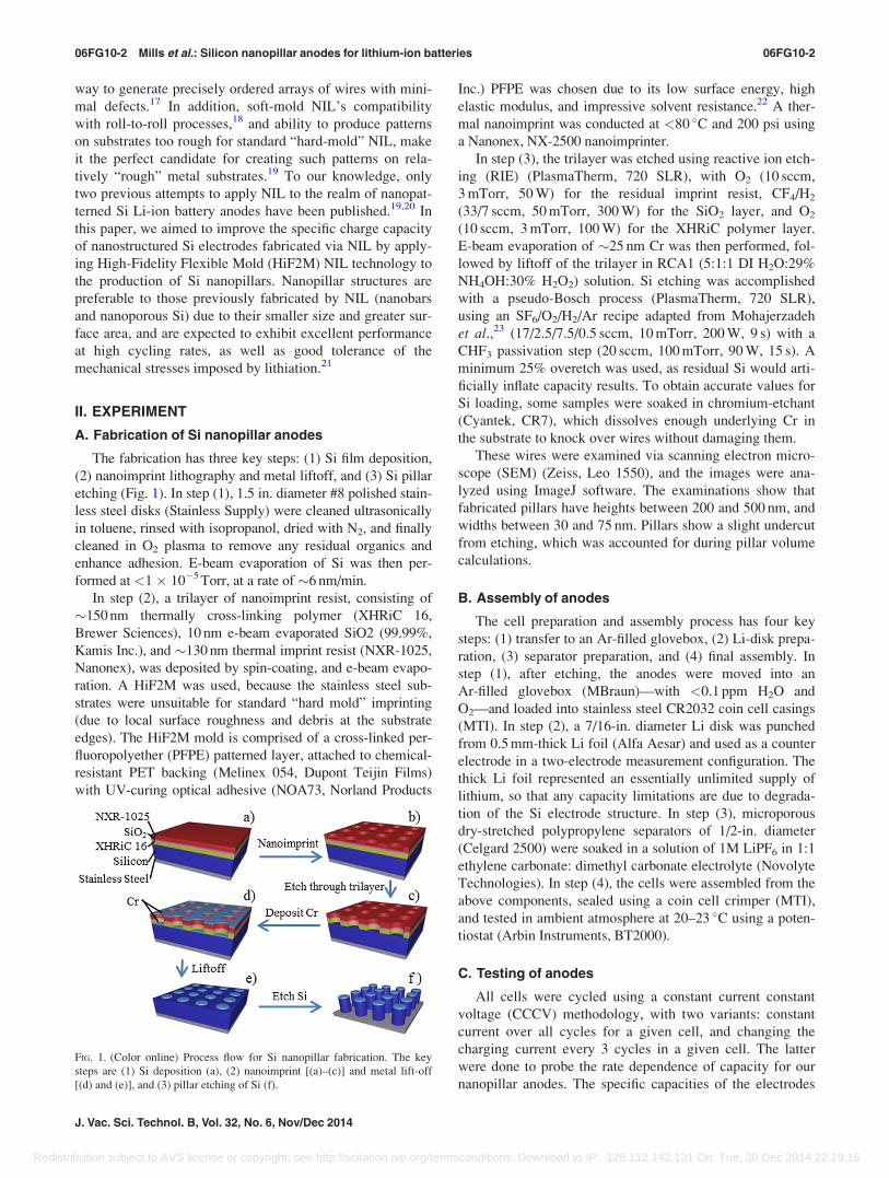
A. Nanopattern transfer onto rough substrates
The as-provided stainless steel disks were unsuitable for
hard-mold NIL, showing 120 nm height variations across the
substrate, in addition to debris from the laser-cutting process
at the disk edges. However, thermal imprint with the HiF2M
molds has achieved large-area high-fidelity pattern transfer,
demonstrated by the SEM micrographs shown in Fig. 2.
Figure 2 shows an SEM micrograph of a pillar pattern trans-
ferred onto one of our highly nonuniform, Si-coated stainless
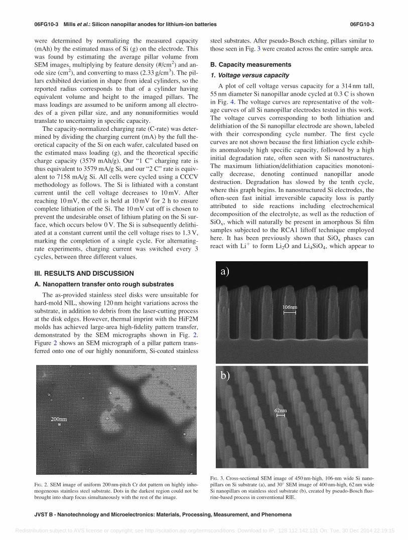
steel substrates. After pseudo-Bosch etching, pillars similar to
those seen in Fig. 3 were created across the entire sample area.
B. Capacity measurements
1. Voltage versus capacity
A plot of cell voltage versus capacity for a 314 nm tall,
55 nm diameter Si nanopillar anode cycled at 0.3 C is shown
in Fig. 4. The voltage curves are representative of the volt-
age curves of all Si nanopillar electrodes tested in this work.
The voltage curves corresponding to both lithiation and
delithiation of the Si nanopillar electrode are shown, labeled
with their corresponding cycle number. The first cycle
curves are not shown because the first lithiation cycle exhib-
its anomalously high specific capacity, followed by a high
initial degradation rate, often seen with Si nanostructures.
The maximum lithiation/delithiation capacities monotoni-
cally decrease, denoting continued nanopillar anode
destruction. Degradation has slowed by the tenth cycle,
where this graph begins. In nanostructured Si electrodes, the
often-seen fast initial irreversible capacity loss is partly
attributed to side reactions including electrochemical
decomposition of the electrolyte, as well as the reduction of
SiOx, which will naturally be present in amorphous Si film
samples subjected to the RCA1 liftoff technique employed
here. It has been previously shown that SiOx phases can
react with Liþ to form Li2O and Li4SiO4, which appear to
FIG. 2. SEM image of uniform 200 nm-pitch Cr dot pattern on highly inho-
mogeneous stainless steel substrate. Dots in the darkest region could not be
brought into sharp focus simultaneously with the rest of the image.
FIG. 3. Cross-sectional SEM image of 450 nm-high, 106-nm wide Si nano-
pillars on Si substrate (a), and 30� SEM image of 400 nm-high, 62 nm wide
Si nanopillars on stainless steel substrate (b), created by pseudo-Bosch fluo-
rine-based process in conventional RIE.
06FG10-3 Mills et al.: Silicon nanopillar anodes for lithium-ion batteries 06FG10-3
JVST B - Nanotechnology and Microelectronics: Materials, Processing, Measurement, and Phenomena
Redistribution subject to AVS license or copyright; see http://scitation.aip.org/termsconditions. Download to IP: 128.112.142.131 On: Tue, 30 Dec 2014 22:19:15
stabilize Si-based anode structures, though at reduced
capacities.24,25
The presence of irreversible side reactions can be quanti-
fied through measurements of coulombic efficiency, which is
the ratio of lithiation capacity to delithiation capacity during a
cycle. The value for our nanopillar Si electrodes is typically
around 80% on the first cycle. Subsequently, the coulombic
efficiency increases rapidly, reaching stable values around
96% after about 10 cycles and remains stable during subse-
quent cycles. The initially low values of coulombic efficiency
support the idea of SiOx reduction, as once the SiOx has been
exhausted, the coulombic efficiency would stabilize. The sta-
ble coulombic efficiency of 96% is indicative of ongoing side
reactions in the cell during cycling. These side reactions likely
proceed through a crack and growth mechanism in which vol-
umetric expansion of the Si electrodes during charging cracks
any formed passivation layers, allowing further electrolyte
decomposition. Increasing the coulombic efficiency of these
electrodes remains a challenge and has previously been
addressed through the fabrication of composite structures.26
2. Specific capacity
The specific capacity for 314 nm tall and 55 nm diameter
nanopillars during cycling is shown in Fig. 5. The data plot-
ted in Fig. 5 represent an average of three cells, with error
bars marking þ/� one standard deviation. The variance in
capacity data is attributed to slight variations to local geome-
try of the nanopillars that occur during processing. The aver-
age initial delithiation capacity of the cells in Fig. 5 was
3100 mAh/g when delithiated between 10 mV and 1.3 V at a
0.3 C rate. This capacity is lower than the theoretical
capacity of Si, but is typical of capacity values reported in
the literature for other nanostructured Si electrodes. The
measured specific capacities of our electrodes are higher
than those previously reported for Si electrodes structured
using NIL. The higher capacities compared with the struc-
tures reported in Refs. 19 and 20 are due at least in part to
our more aggressive utilization of our Si electrodes. In both
Refs. 19 and 20, the extent of lithiation of their electrodes
was limited in order to help improve capacity retention.
Note that other Si nanopillar electrodes with varying diame-
ter and pillar heights were fabricated and tested, but no cor-
relations between specific capacity and these parameters
were observed within our range of fabrication dimensions.
Figure 5 shows the cell performance at three different
cycling rates (0.3 C, 0.7 C, and 1.4 C), where the rate is
switched every 3 cycles. Cycling the cells at different rates
demonstrates the rate capability of our Si electrodes, with
large capacity drops at faster rates being indicative of higher
cell impedance. Our nanopillar electrodes show a drop in
capacity of about 5% when the cycling rate is increased by a
factor of 4.6 from 0.3 to 1.4 C. This is significantly improved
over previous Si electrodes fabricated by NIL, which have
shown drops in capacity between 25% and 40% over similar
ranges of charging rates. This increase in rate capability is
attributed to the lower characteristic lengths for both solid
phase lithium diffusion in our Si structures, and liquid phase
ion diffusion between the Si nanopillars, compared to previ-
ously reported NIL-fabricated electrode geometries. From a
simple 1D diffusion standpoint, complete diffusion into a
50 nm-diameter pillar should take less than a minute, given a
Liþ diffusion coefficient on the order of 10�11 cm2/s in Si.27
C. Capacity retention
The capacity of the Si electrodes in Fig. 5 can be seen to
decay during cycling, with “nanopillar”-labeled samples
approaching 60% of their initial capacity by 50 cycles. This
loss of 40% capacity is attributed to degradation of the Si
electrode structure, presumably through loss of electrical
contact to portions of the Si.
The attribution of the capacity fade to contact loss follows
from the fact that other degradation mechanisms such as loss
FIG. 5. (Color online) Gravimetric capacity data for 314 nm tall and 55 nm
diameter nanopillars over a period of 50 cycles, compared with capacity val-
ues for other NIL-fabricated samples from the literature (Refs. 19 and 20).
FIG. 4. (Color online) Charge/discharge curves for 314 nm high and 55 nm
diameter nanopillars. Shown are the curves for the tenth, 20th, 30th, and
40th lithiation and delithiation cycles. Note the lithiation and delithiation
curves shift to the left with increasing cycle number, denoting Si
degradation.
06FG10-4 Mills et al.: Silicon nanopillar anodes for lithium-ion batteries 06FG10-4
Redistribution subject to AVS license or copyright; see http://scitation.aip.org/termsconditions. Download to IP: 128.112.142.131 On: Tue, 30 Dec 2014 22:19:15
of lithium inventory and impedance rise can be ruled out.
Loss of lithium inventory is ruled out because the lithium foil
counter electrode in the cells acts as an essentially infinite
source of lithium. Impedance rise is ruled out by Fig. 5, which
shows no significant changes in rate capability during cycling.
Significant rises in impedance would manifest themselves as
a more severe reduction in capacity when stepping to higher
cycling rates. The electrical contact loss is a consequence of
the high volume expansion of the electrodes and can proceed
through either fracturing of the Si features or delamination of
the features from the stainless steel current collector. Due to
the small characteristic dimensions of the electrodes, it is
assumed that fracture is unlikely and that delamination from
the current collector is the more likely cause.
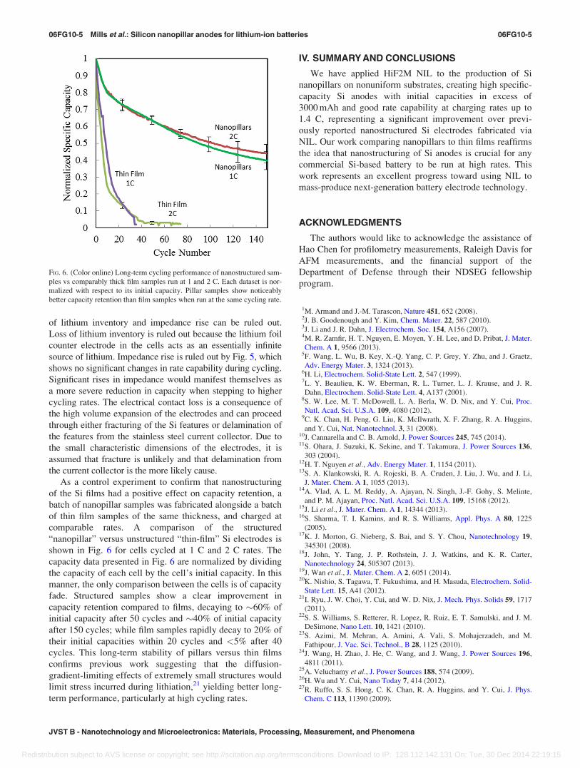
As a control experiment to confirm that nanostructuring
of the Si films had a positive effect on capacity retention, a
batch of nanopillar samples was fabricated alongside a batch
of thin film samples of the same thickness, and charged at
comparable rates. A comparison of the structured
“nanopillar” versus unstructured “thin-film” Si electrodes is
shown in Fig. 6 for cells cycled at 1 C and 2 C rates. The
capacity data presented in Fig. 6 are normalized by dividing
the capacity of each cell by the cell’s initial capacity. In this
manner, the only comparison between the cells is of capacity
fade. Structured samples show a clear improvement in
capacity retention compared to films, decaying to �60% of
initial capacity after 50 cycles and �40% of initial capacity
after 150 cycles; while film samples rapidly decay to 20% of
their initial capacities within 20 cycles and <5% after 40
cycles. This long-term stability of pillars versus thin films
confirms previous work suggesting that the diffusion-
gradient-limiting effects of extremely small structures would
limit stress incurred during lithiation,21 yielding better long-
term performance, particularly at high cycling rates.
IV. SUMMARY AND CONCLUSIONS
We have applied HiF2M NIL to the production of Si
nanopillars on nonuniform substrates, creating high specific-
capacity Si anodes with initial capacities in excess of
3000 mAh and good rate capability at charging rates up to
1.4 C, representing a significant improvement over previ-
ously reported nanostructured Si electrodes fabricated via
NIL. Our work comparing nanopillars to thin films reaffirms
the idea that nanostructuring of Si anodes is crucial for any
commercial Si-based battery to be run at high rates. This
work represents an excellent progress toward using NIL to
The authors would like to acknowledge the assistance of
Hao Chen for profilometry measurements, Raleigh Davis for
AFM measurements, and the financial support of the
Department of Defense through their NDSEG fellowship
program.
1M. Armand and J.-M. Tarascon, Nature 451, 652 (2008).2J. B. Goodenough and Y. Kim, Chem. Mater. 22, 587 (2010).3J. Li and J. R. Dahn, J. Electrochem. Soc. 154, A156 (2007).4M. R. Zamfir, H. T. Nguyen, E. Moyen, Y. H. Lee, and D. Pribat, J. Mater.
Chem. A 1, 9566 (2013).5F. Wang, L. Wu, B. Key, X.-Q. Yang, C. P. Grey, Y. Zhu, and J. Graetz,
Adv. Energy Mater. 3, 1324 (2013).6H. Li, Electrochem. Solid-State Lett. 2, 547 (1999).7L. Y. Beaulieu, K. W. Eberman, R. L. Turner, L. J. Krause, and J. R.
Dahn, Electrochem. Solid-State Lett. 4, A137 (2001).8S. W. Lee, M. T. McDowell, L. A. Berla, W. D. Nix, and Y. Cui, Proc.
Natl. Acad. Sci. U.S.A. 109, 4080 (2012).9C. K. Chan, H. Peng, G. Liu, K. McIlwrath, X. F. Zhang, R. A. Huggins,
and Y. Cui, Nat. Nanotechnol. 3, 31 (2008).10J. Cannarella and C. B. Arnold, J. Power Sources 245, 745 (2014).11S. Ohara, J. Suzuki, K. Sekine, and T. Takamura, J. Power Sources 136,
303 (2004).12H. T. Nguyen et al., Adv. Energy Mater. 1, 1154 (2011).13S. A. Klankowski, R. A. Rojeski, B. A. Cruden, J. Liu, J. Wu, and J. Li,
J. Mater. Chem. A 1, 1055 (2013).14A. Vlad, A. L. M. Reddy, A. Ajayan, N. Singh, J.-F. Gohy, S. Melinte,
and P. M. Ajayan, Proc. Natl. Acad. Sci. U.S.A. 109, 15168 (2012).15J. Li et al., J. Mater. Chem. A 1, 14344 (2013).16S. Sharma, T. I. Kamins, and R. S. Williams, Appl. Phys. A 80, 1225
(2005).17K. J. Morton, G. Nieberg, S. Bai, and S. Y. Chou, Nanotechnology 19,
345301 (2008).18J. John, Y. Tang, J. P. Rothstein, J. J. Watkins, and K. R. Carter,
Nanotechnology 24, 505307 (2013).19J. Wan et al., J. Mater. Chem. A 2, 6051 (2014).20K. Nishio, S. Tagawa, T. Fukushima, and H. Masuda, Electrochem. Solid-
State Lett. 15, A41 (2012).21I. Ryu, J. W. Choi, Y. Cui, and W. D. Nix, J. Mech. Phys. Solids 59, 1717
(2011).22S. S. Williams, S. Retterer, R. Lopez, R. Ruiz, E. T. Samulski, and J. M.
DeSimone, Nano Lett. 10, 1421 (2010).23S. Azimi, M. Mehran, A. Amini, A. Vali, S. Mohajerzadeh, and M.
Fathipour, J. Vac. Sci. Technol., B 28, 1125 (2010).24J. Wang, H. Zhao, J. He, C. Wang, and J. Wang, J. Power Sources 196,
4811 (2011).25A. Veluchamy et al., J. Power Sources 188, 574 (2009).26H. Wu and Y. Cui, Nano Today 7, 414 (2012).27R. Ruffo, S. S. Hong, C. K. Chan, R. A. Huggins, and Y. Cui, J. Phys.
Chem. C 113, 11390 (2009).
FIG. 6. (Color online) Long-term cycling performance of nanostructured sam-
ples vs comparably thick film samples run at 1 and 2 C. Each dataset is nor-
malized with respect to its initial capacity. Pillar samples show noticeably
better capacity retention than film samples when run at the same cycling rate.
06FG10-5 Mills et al.: Silicon nanopillar anodes for lithium-ion batteries 06FG10-5
JVST B - Nanotechnology and Microelectronics: Materials, Processing, Measurement, and Phenomena
Redistribution subject to AVS license or copyright; see http://scitation.aip.org/termsconditions. Download to IP: 128.112.142.131 On: Tue, 30 Dec 2014 22:19:15