SPECIAL SECTION ON NANOBIOSENSORS Received November 10, 2014, accepted March 24, 2015, date of current version April 22, 2015. Digital Object Identifier 10.1109/ACCESS.2015.2422842 Silicon Nanowire Field-Effect Transistors— A Versatile Class of Potentiometric Nanobiosensors LUYE MU 1,2 , YE CHANG 1 , SONYA D. SAWTELLE 3 , MATHIAS WIPF 2 , XUEXIN DUAN 1 , AND MARK A. REED 2 , (Senior Member, IEEE) 1 State Key Laboratory of Precision Measuring Technology and Instruments, Tianjin University, Tianjin 300072, China 2 Department of Electrical Engineering, Yale University, New Haven, CT 06520, USA 3 Department of Applied Physics, Yale University, New Haven, CT 06520, USA Corresponding author: X. Duan ([email protected]) This work was supported in part by the Tianjin Applied Basic Research and Advanced Technology under Grant 14JCYBJC41500 and in part by the 111 Project under Grant B07014. The work of L. Mu was supported by the Natural Sciences and Engineering Council of Canada. The work of M. A. Reed was supported in part by the Research Project under Grant FA8650-9-D-5037 0019 and in part by the U.S. Army Research Office under Grant MURI W911NF-11-1-0024. ABSTRACT Silicon nanowire field-effect transistors (Si-NW FETs) have been demonstrated as a versatile class of potentiometric nanobiosensors for real time, label-free, and highly sensitive detection of a wide range of biomolecules. In this review, we summarize the principles of such devices and recent developments in device fabrication, fluid integration, surface functionalization, and biosensing applications. The main focus of this review is on CMOS compatible Si-NW FET nanobiosensors. INDEX TERMS Biosensors, field effect transistors, nanowires, semiconductor nanostructures, nanobiosensors. I. INTRODUCTION The role of biosensing in society has gained increasing importance over the last several decades, reflected in the rapid growth of the global market. According to Global Industry Analysts, Inc., the global market for biosensor devices is expected to reach $20 billion by the year 2020. Sensitive detection and quantification of bio-analytes is a driving force for innovation in many vital fields such as biomedical research, clinical medicine, agriculture, food safety, environmental monitoring and homeland security. Across these diverse applications of biosensors, there is a common demand for properties such as high sensitivity, low detection limit, large dynamic range, rapid and real- time detection, low cost and miniaturization. Modern advancements in nanomaterials and nano-scale fabrication have enabled a new generation of biosensors that can more easily satisfy these needs through improved performance, smaller size, and novel functionality. These nanobiosensors are sub-micrometer sized in at least one dimension, which allows them to possess very large surface area to volume ratios. In many cases their small footprint makes them well suited for high-density sensor arrays, lab-on-chip systems, and single-cell interfacing. Classification schemes for biosensors traditionally focus on either the biological element e.g. antibody, enzyme, or nucleic acid, or on the transducing element e.g. potentiometric, amperometric, or fluorometric transduc- tion [1]. Although the operation of the biological element can vary, all potentiometric biosensors utilize a transduction element that operates under a change in electrical potential between a reference electrode and a working surface. This category encompasses all varieties of ion-selective electrodes (ISEs) and ion-sensitive field effect transistors (ISFETs). An ISE is a two-terminal system wherein the voltage between the membrane-enclosed indicator and reference electrode is modulated by the activity of ions with respect to the selective membrane. In contrast, ISFETs employ a three-terminal configuration with an active channel whose current is modulated in the presence of charged species. The advantage of an ISFET over an ISE is that an FET has intrinsic amplification. We also note here that the requirement of electrical charge for potentiometric transduction does not significantly restrict applications in that most biomacromolecules and cells acquire a net charge in solution at physiological pH. Clever modifications can also enable sensing of neutral molecules on some of these platforms [2]–[4]. Nanobiosensors falling under the ISFET umbrella include quasi-1D FETs utilizing top-down and bottom-up semiconducting wires, conducting polymer wires or carbon VOLUME 3, 2015 2169-3536 2015 IEEE. Translations and content mining are permitted for academic research only. Personal use is also permitted, but republication/redistribution requires IEEE permission. See http://www.ieee.org/publications_standards/publications/rights/index.html for more information. 287
Transcript
SPECIAL SECTION ON NANOBIOSENSORS
Received November 10, 2014, accepted March 24, 2015, date of current version April 22, 2015.
Digital Object Identifier 10.1109/ACCESS.2015.2422842
Silicon Nanowire Field-Effect Transistors—A Versatile Class of PotentiometricNanobiosensorsLUYE MU1,2, YE CHANG1, SONYA D. SAWTELLE3, MATHIAS WIPF2, XUEXIN DUAN1,AND MARK A. REED2, (Senior Member, IEEE)1State Key Laboratory of Precision Measuring Technology and Instruments, Tianjin University, Tianjin 300072, China2Department of Electrical Engineering, Yale University, New Haven, CT 06520, USA3Department of Applied Physics, Yale University, New Haven, CT 06520, USA
This work was supported in part by the Tianjin Applied Basic Research and Advanced Technology under Grant 14JCYBJC41500 and inpart by the 111 Project under Grant B07014. The work of L. Mu was supported by the Natural Sciences and Engineering Council ofCanada. The work of M. A. Reed was supported in part by the Research Project under Grant FA8650-9-D-5037 0019 andin part by the U.S. Army Research Office under Grant MURI W911NF-11-1-0024.
ABSTRACT Silicon nanowire field-effect transistors (Si-NW FETs) have been demonstrated as a versatileclass of potentiometric nanobiosensors for real time, label-free, and highly sensitive detection of a wide rangeof biomolecules. In this review, we summarize the principles of such devices and recent developments indevice fabrication, fluid integration, surface functionalization, and biosensing applications. The main focusof this review is on CMOS compatible Si-NW FET nanobiosensors.
INDEX TERMS Biosensors, field effect transistors, nanowires, semiconductor nanostructures,nanobiosensors.
I. INTRODUCTIONThe role of biosensing in society has gained increasingimportance over the last several decades, reflected in therapid growth of the global market. According to GlobalIndustry Analysts, Inc., the global market for biosensordevices is expected to reach $20 billion by the year 2020.Sensitive detection and quantification of bio-analytes is adriving force for innovation in many vital fields such asbiomedical research, clinical medicine, agriculture, foodsafety, environmental monitoring and homeland security.Across these diverse applications of biosensors, there is acommon demand for properties such as high sensitivity,low detection limit, large dynamic range, rapid and real-time detection, low cost and miniaturization. Modernadvancements in nanomaterials and nano-scale fabricationhave enabled a new generation of biosensors that can moreeasily satisfy these needs through improved performance,smaller size, and novel functionality. These nanobiosensorsare sub-micrometer sized in at least one dimension, whichallows them to possess very large surface area to volumeratios. In many cases their small footprint makes them wellsuited for high-density sensor arrays, lab-on-chip systems,and single-cell interfacing.
Classification schemes for biosensors traditionally focuson either the biological element e.g. antibody, enzyme,
or nucleic acid, or on the transducing element e.g.potentiometric, amperometric, or fluorometric transduc-tion [1]. Although the operation of the biological elementcan vary, all potentiometric biosensors utilize a transductionelement that operates under a change in electricalpotential between a reference electrode and a workingsurface. This category encompasses all varieties ofion-selective electrodes (ISEs) and ion-sensitive field effecttransistors (ISFETs). An ISE is a two-terminal systemwherein the voltage between the membrane-enclosedindicator and reference electrode is modulated by the activityof ions with respect to the selective membrane. In contrast,ISFETs employ a three-terminal configuration with an activechannel whose current is modulated in the presence ofcharged species. The advantage of an ISFET over an ISE isthat an FET has intrinsic amplification. We also note herethat the requirement of electrical charge for potentiometrictransduction does not significantly restrict applications inthat most biomacromolecules and cells acquire a net chargein solution at physiological pH. Clever modifications canalso enable sensing of neutral molecules on some of theseplatforms [2]–[4].
Nanobiosensors falling under the ISFET umbrellainclude quasi-1D FETs utilizing top-down and bottom-upsemiconducting wires, conducting polymer wires or carbon
VOLUME 3, 20152169-3536 2015 IEEE. Translations and content mining are permitted for academic research only.
Personal use is also permitted, but republication/redistribution requires IEEE permission.See http://www.ieee.org/publications_standards/publications/rights/index.html for more information.
287
L. Mu et al.: Si-NW FETs—A Versatile Class of Potentiometric Nanobiosensors
nanotubes (CNTs) and 2D FETs which utilize naturally2D materials. The 1D FETs are claimed to benefit froman extreme surface area to volume ratio which permitseffective channel gating from even just a few adsorbed analytemolecules. Cui et al. were the first to execute this geometry:In 2001 they used vapor-liquid-solid (VLS) grown siliconnanowires (Si-NWs) for pH sensing and detected the bindingof streptavidin protein on biotin-labeled wires [5]. Such‘‘bottom-up’’ style FETs have since been used for the fullspectrum of biosensing applications (i.e. detection of DNA,antibodies, enzymes, cells, aptamers, bioelectricity, etc.) withcharged based or electrochemical sensing [6]–[8]. Relativelysoon after, the top-down fabricated nanowire FET wasintroduced as a sensing platform [9]–[11] in order to addressthe problems of placement, integration, and reproducibilityencountered with bottom-up materials. Such concerns applyequally to the CNT 1D FETs, in addition to the challengeof chiral vector selection, but nonetheless they havebeen demonstrated in a wide variety of biosensingniches [12]–[17]. Most recently, 1D FETs using polymericnanowires have been developed, which enjoy cheaperfabrication and more customizable functionalization thansemiconductor wires, but exhibit inferior electricalproperties [18]–[21].
The 2D graphene-based FETs exhibit an enhanced surfacesensitivity like the 1D FETs, as well as possess a minimalband-gap and high in-plane carrier mobility derived fromthe confinement of the carbon lattice [22]. These deviceshave been utilized for pH sensing [23], [24], as a possiblereference electrode [25], as well as specific protein [26], [27]and DNA [28]–[30] sensing. Using graphene FETs,Huang et al. have demonstrated redox-based glucosedetection with an enzyme-functionalized surface [31] andCohen-Karni et al. have provided a dramatic demonstrationof cell-interfacing by monitoring the electrical activity ofembryonic heart cells [32]. Recently 2D FETs using a singlemonolayer sheet of molybdenum disulfide (MoS2) as theactive channel have been employed for pH sensing andaqueous label-free protein detection in the femtomolarrange [33].
Within the ISE class of potentiometric sensors,nanotechnology has led to rationally designed solid statemembrane nanopores [34], [35], and improved solid-contactelectrode materials such as CNTs [36], [37] and goldnanoparticles [38]. These refinements to the conventionalISEs notwithstanding, we choose to focus this review onthe ISFET class where nanotechnology has had a moretransformative impact, and in particular the silicon nanowirevariety due to manufacturability. We provide first a briefoverview of the general FET sensing structure, and then theparticulars of Si-NW FET fabrication. A short discussionof fluidic integration, multiplexing, functionalization, andperformance limitations is followed by a survey of the variousbiological applications that have been successfully addressedby Si-NW FETs. A discussion of Si-NW FETs compared toother biosensing platforms can be found elsewhere [39].
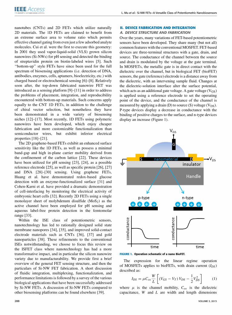
II. DEVICE FABRICATION AND INTEGRATIONA. DEVICE STRUCTURE AND FABRICATIONOver the years, many variations of FET-based potentiometricsensors have been developed. They share many (but not all)common features with the conventionalMOSFET. FET-baseddevices are three-terminal structures with a gate, drain, andsource. The conductance of the channel between the sourceand drain is modulated by the voltage at the gate terminal.In MOSFETs, the metallic gate is in direct contact with thedielectric over the channel, but in biological FET (bioFET)sensors, the gate (reference) electrode is a distance away fromthe dielectric, with an intervening sample fluid. Changes atthe dielectric-solution interface alter the surface potential,which acts as an additional gate voltage. A gate voltage (VGS)is applied using a reference electrode to set the operatingpoint of the device, and the conductance of the channel ismeasured by applying a drain (D) to source (S) voltage (VDS).P-type devices display a decrease in conductance with thebinding of positive charges to the surface, and n-type devicesdisplay an increase (Figure 1).
FIGURE 1. Operation schematic of a nano BioFET.
The expression for the linear regime operationof MOSFETs applies to bioFETs, with drain current (IDS )described as:
IDS = µCoxWL
[(VGS − VT )VDS −
12V 2DS
](1)
where µ is the channel mobility, Cox is the dielectriccapacitance, W and L are width and length dimensions
288 VOLUME 3, 2015
L. Mu et al.: Si-NW FETs—A Versatile Class of Potentiometric Nanobiosensors
of the device, and VT is the threshold voltage of thedevice. When the device is exposed to solution, a surfacepotential (ψ) develops at the dielectric-solution interface,which is a function of surface and solution characteristics.Thus, the VT in (1) can be expressed as:
VT = Eref − ψ + χ sol −8Si
q−
QtCox+ 2φf (2)
where Eref is the reference electrode potential, χ sol is thesurface dipole potential of the solvent, 8Si is the channelwork function, q is elementary charge,Qt is a combination ofdepletion charges in the semiconductor, accumulated chargesin the dielectric, and interface trap charges, and φf is theFermi potential. In the case where gate and drain voltages arefixed, the only variable term in the equation is ψ , which isa function of physical and chemical changes at the surfaceof the oxide. Thus, monitoring changes via the change inVT is an effective way of sensing changes at the dielectric-electrolyte interface.
Over time, variations on the bioFET has been developedto allow for the detection of many analytes, these variations,such as enzyme-FETs, chemical-FETs, etc., are realized byfunctionalizing different specific receptors at the dielectric-solution interface. The difference between different types ofnano FET-based sensors lies mainly with the interface andchannel material. Out of all the bioFETs that have beenstudied, micro- and nanofabricated silicon has been the mostpopular material for the channel.
Approaches to fabricating Si-NW for sensors have beencategorized into two main groups: bottom up and top downassembly. The first Si-NW FETs were grown by bottomup VLS techniques [5], [40], then harvested and depositedon a substrate. The contacts were subsequently patternedby lithography. VLS synthesis techniques nominally usemetal nanoparticles to catalyze nanowire formation anddefine nanowire size. High quality nanowires with low defectdensities and smooth sidewalls can be fabricated this way,however this technique is not conducive to scaling formass production. Various approaches have been proposedto aid the arrangement of 1D nanomaterials on a substrate,including many fluidic assisted [41]–[45] and electricallycontrolled [46]–[48] methods. Nevertheless, the yield andrepeatability was still not optimal. This led to an increase inthe use of top down device fabrication technologies, whichallowed nanowire dimensions and locations to be preciselydefined on the wafer. Top-down fabricated nanowires aretypically defined on ultrathin silicon on insulator (UTSOI)wafers using electron beam lithography (EBL), with thecontacts and metallization defined using opticallithography [10], [49], [50]. In order to further reducedimensions, a subsequent wet chemical etch [11], [51]–[53],electrochemical etch [54], or oxidation [55], [56] isoften used. Unfortunately, EBL is an expensive andtime-consuming process, and is not amenable to large-scalemanufacturing. Therefore several groups have innovatedsome creative process flows for fabricating nanowires based
on the anisotropy of silicon and plane-dependent wet etching,without needing EBL. For example, Chen et al. used aSi3N4 etch mask patterned by conventional lithography togenerate nanoribbons, followed by anisotropic wet etchingand thermal oxidation to define two triangular cross-sectionnanowires from the edges of each nanoribbon [57].Stern et al. also used a mask-and-etch method to fabricatenanowires from optically defined nanoribbons, usingtetramethylammonium hydroxide (TMAH) [11]. Anotheradvantage of using a highly anisotropic etching methodinstead of oxidation is that it also provides refinement ofnanowire edges. For instance, in addition to thinning thenanowires, TMAH also provided a smoothing effect forsidewall imperfections not aligned to the exposed [111] plane,creating sensitive structures with extremely low noise [58].Recently, many groups have opted to use larger width devicessuch as nanoribbons and nanoplates, with much more relaxedfabrication requirements [59]–[61].
Although single-crystalline silicon nanowires have greatsignal to noise ratios, their fabrication incurs significant costsdue to the need for UTSOI wafers as starting materials.Therefore, polysilicon nanowires have been explored as acheaper alternative. Amorphous silicon of approximately100 nm thickness can be deposited on oxide substrates bylow pressure chemical vapor deposition (LPCVD), annealedto form grains, then subsequently etched to form wires [62].Just like with single-crystalline nanowires, various masking,trimming and spacer techniques have been used to definesub-micron dimension wires in polysilicon [62]–[64].However, one would expect the intrinsic noise ofpolycrystalline nanowires to be inferior compared to singlecrystalline nanowires due to the increased grain-boundariesand interface traps. A way to fabricate single crystallineSi-NW FET biosensors without needing to use UTSOI isto create fin-like structures from bulk silicon (ie. FinFETs).Rigante et al. showed fully-depleted bio-FinFETs withcritical dimensions of ∼20 nm with excellent electricalproperties [65].
In the context of modern integrated circuit technology,there is significant value in making the device fabricationCMOS-compatible. Many groups have developedCMOS-compatible process flows [11], [51], [61], [64]–[66],and some have successfully integrated on-chip memorycomponents with the sensors [67]. Huang et al. usedthe 0.35 µm 2P4M standard CMOS process to fabricate apolysilicon NW based biosensor system-on-a-chip completewith an amplifier, an analog to digital converter, a microcon-troller, and a wireless transceiver [68].With the advantages ofscalability and potential integration with on-chip addressingand signal processing components, CMOS compatibleSi-NW FETs can meet the current demand for a sensitive,high-throughput and multiplexed biosensor. Similar devicecharacteristics allow the use of a global gating scheme inmultiplexing, and various calibration methods can be usedto account for the small device-to-device variations anddrift [69].
VOLUME 3, 2015 289
L. Mu et al.: Si-NW FETs—A Versatile Class of Potentiometric Nanobiosensors
The dielectric coating over the channel is one of the keycomponents dictating the performance of the Si-NW device.Traditionally, SiO2 is used due to the ease of fabricationvia oxidation. However, SiO2 is semipermeable to smallpositive ions such as K+ and Na+, thus significantlylimiting device stability and lifetime when operating in highionic strength solutions. High k dielectrics such as Si3N4,Al2O3, and HfO2, are known to improve device leakage,stability, and hysteresis due to the high quality and density offilms [70], [71]. In addition, many of them exhibitnear-Nernstian responses to pH [59], [72]–[74]. The mostpopular method for depositing good quality high k dielectricsis by atomic layer deposition (ALD), a self-limitingprocess capable of creating uniform, dense, conformal, andpin-hole free layers. Nevertheless, since high k dielectricsare deposited rather than grown, the interface between thechannel and the dielectric is rarely good enough quality tomatch that of Si-SiO2, thereby increasing interface traps anddevice noise. Therefore, the correct dielectric to use for asensor is highly dependent on the application – SiO2 covereddevices may have better signal to noise ratios for shortterm operations for detecting biomolecules, whereas high kcovered devices may have better signal to noise ratios forlong term operations or pH-based measurements. Somegroups have investigated multi-layer dielectric stacks tosimultaneously take advantage of the excellent Si-SiO2interface and high k layer qualities [71].
For the remainder of this review, we focus mainly onsensing examples from top-down fabricated silicon nanowires.However, since most biomolecular detection schemes canbe generally applied to all FET-type sensors regardless offabrication method or device material, we have also includeda few notable examples of works from bottom up nanowiresand nanowires made from other channel materials.
B. FLUIDIC INTEGRATIONSample scarcity is often an issue for biological samples –in particular physiological samples. Therefore, being ableto limit the required sample amount for analysis isadvantageous. BioFETs can bemade into planar, high-densityarrays, which are conducive to microfluidic integration. Twotypes of microfluidic setups are commonly used for sampledelivery: reservoirs and microchannels. The fluid cells aretypically made from polydimethylsiloxane (PDMS) due to itsexcellent optical transparency and biocompatibility.
Reservoirs over FET devices are typically designed tohold a few to hundreds of microliters of sample, and sampleexchange is done manually through pipetting [11], [75].Drawbacks of the microwell method include evaporation ofsample, which precludes long termmeasurements from beingconducted on small samples, and difficulty in conductingkinetic measurements due to the consumption of analytes.
Microchannels have micrometer dimensions, but requiremore reagent overall due to the need for continuous flow.Flow-based delivery allows greater potential for systemautomation, with accurate sample volume dispensing
and automatic sample switching [76]. However, flow inmicrofluidic channels can be laminar, which can restrictthe interaction between the injected molecules and thesensor surface [77]. It was also shown that variation in flowspeed induces a change in conductance in the underlyingFET [76], [78]. However, many groups used constant speedflow to deliver solutions, and were able to obtain consistentresults at low sample concentrations [76], [79]–[81].
The integration of a reference electrode is an essentialyet nontrivial component of fluidic integration forSi-NW FETs. In open reservoir sensing, the solution gateelectrode can be inserted directly into the open reservoir.However, in flow experiments, the reference electrode iseither integrated into the inlet/outlet tubing [82]–[84], orfabricated on-chip. Although on-chip Ag/AgCl referenceelectrodes have been reported [85], the use of any metal(typically gold or platinum) with a differential setup mayoffer a more robust technique due to the ability to decoupleother environmental factors [76]. The ability to create aneffective differential system is directly dependent on theability to control surface functionalization across an array ofdevices.
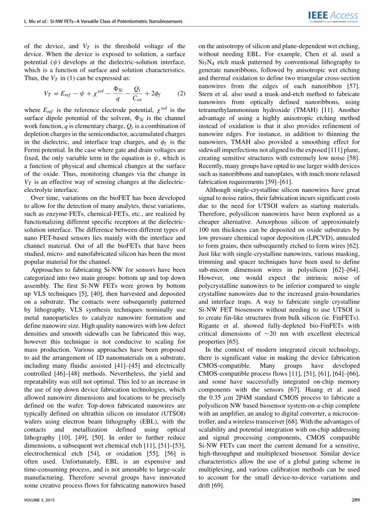
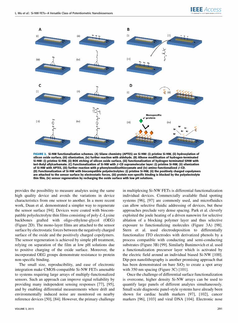
C. FUNCTIONALIZATIONIn order to detect specific biomolecular interactions,nanowire devices need to be functionalized withbio-receptors. The choice of functionalization schemeand specifics of the procedure affect the quality of thebio-receptor layer e.g. density, thickness and orientation.In turn, this layer strongly impacts performance metricsof the sensor such as sensitivity, stability, reproducibilityand regenerative capacity [86], [87]. Different strategieshave been applied for Si-NW surface functionalization [88].For silicon oxide surfaces, covalent modification throughsilane chemistry has been the most common technique(Figure 2A). A typical silane agent is 3-aminopropyltrie-thoxysilane (APTES). APTES introduces a primary amineterminal group, which can further react with aldehyde,carboxylic acid and epoxy groups present on proteins andother biomolecules. Dorvel et al. compared the effect of dif-ferent linker chemistries on protein sensing performance [89].Additionally, 3-mercaptopropyl-trimethoxysilane (MPTMS),(3-Glycidoxypropyl)-methyl-diethoxysilane (GPTS) and(3-bromopropyl)trichlorosilane have been reported tointroduce thiol [90], epoxy [91] and bromide [92] terminalgroup, respectively. Alternatively, for hydrogen-terminatedSi-NWs (oxide free nanowires), alkenes (or alkynes) canbe used to form a true organic monolayer with higherchemical stability compared with silane chemistry alkenes(Figure 2B) [86]. In addition to covalent attachments, somenon-covalent approaches are also noteworthy. For instance,β-cyclodextrin (β-CD) based supramolecular layers havebeen used as linkers for Si-NWs (Figure 2C) [93]. Owingto the reversible host-guest chemistry of β-CD, the sensorsurface can be fully regenerated. Regeneration of the sensorsurface would be highly beneficial for their use, since it
290 VOLUME 3, 2015
L. Mu et al.: Si-NW FETs—A Versatile Class of Potentiometric Nanobiosensors
FIGURE 2. Si-NW functionalization schemes. (A) Silane chemistry (APTES) on Si-NW: (i) pristine Si-NW, (ii) hydroxylation ofsilicon oxide surface, (iii) silanization, (iv) further reaction with aldehyde. (B) Alkene modification of hydrogen-terminatedSi-NW: (i) pristine Si-NW, (ii) BOE etching of silicon oxide surface, (iii) functionalization of hydrogen terminated SiNW withtert-Butyl allylcarbamate. (C) Functionalization of Si-NW with β-CD supramolecular layer: (i) pristine Si-NW, (ii) silanizationof Si-NW with APTES, (iii) further reaction with p-phenylenediisothiocyanate and (iv) amino-functionalized β-CD.(D) Functionalization of Si-NW with biocompatible polyelectrolytes: (i) pristine Si-NW, (ii) the positively charged copolymersare attached to the sensor surface by electrostatic forces, (iii) protein non-specific binding is blocked by the polyelectrolytethin film, (iv) sensor regeneration by recharging the oxide surface with low pH solutions.
provides the possibility to measure analytes using the samehigh quality device and avoids the variations in devicecharacteristics from one sensor to another. In a more recentwork, Duan et al. demonstrated a simpler way to regeneratethe sensor surface [94]. Devices were coated with biocom-patible polyelectrolyte thin films consisting of poly-L-Lysinebackbones grafted with oligo-ethylene-glycol (OEG)(Figure 2D). The mono-layer films are attached to the sensorsurface by electrostatic forces between the negatively chargedsurface of the oxide and the positively charged copolymers.The sensor regeneration is achieved by simple pH treatment,relying on separation of the film at low pH solutions dueto positive charging of the oxide surface. Moreover, theincorporated OEG groups demonstrate resistance to proteinnon-specific binding.
The small size, reproducibility, and ease of electronicintegration make CMOS-compatible Si-NW FETs amenableto systems requiring large arrays of multiply-functionalizedsensors. Such an approach can improve signal reliability byproviding many independent sensing responses [77], [95],and by enabling differential measurements where drift andenvironmentally induced noise are monitored on nearbyreference devices [50], [84]. However, the primary challenge
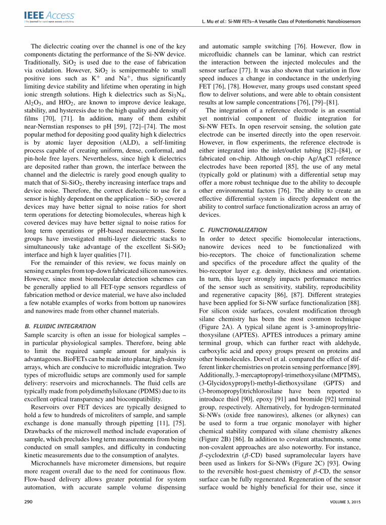
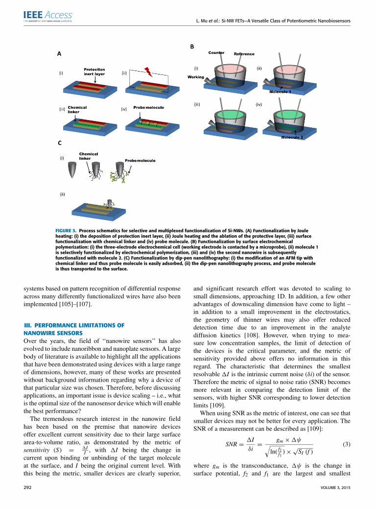
in multiplexing Si-NW FETs is differential functionalizationindividual devices. Commercially available fluid spottingsystems [96], [97] are commonly used, and microfluidicscan allow selective fluidic addressing of devices, but theseapproaches preclude very dense spacing. Park et al. cleverlyexploited the joule heating of a driven nanowire for selectiveablation of a blocking polymer layer and thus selectiveexposure to functionalizing molecules (Figure 3A) [98].Stern et al. used electrodeposition to differentiallyfunctionalize ITO electrodes with derivatized phenols by aprocess compatible with conducting and semi-conductingsubstrates (Figure 3B) [99]. Similarly Bunimovich et al. useda functionalization precursor layer which is activated bythe electric field around an individual biased Si-NW [100].Dip-pen nanolithography is another promising approach thathas been demonstrated on bare SiO2 to create a spot arraywith 350 nm spacing (Figure 3C) [101].
Once the challenge of differential surface functionalizationis overcome, higher density Si-NW arrays can be used toquantify large panels of different analytes simultaneously.Small scale diagnostic panel-style systems have already beenshown for cardiac health markers [97], [102], cancermarkers [96], [103] and viral DNA [104]. Electronic nose
VOLUME 3, 2015 291
L. Mu et al.: Si-NW FETs—A Versatile Class of Potentiometric Nanobiosensors
FIGURE 3. Process schematics for selective and multiplexed functionalization of Si-NWs. (A) Functionalization by Jouleheating: (i) the deposition of protection inert layer, (ii) Joule heating and the ablation of the protective layer, (iii) surfacefunctionalization with chemical linker and (iv) probe molecule. (B) Functionalization by surface electrochemicalpolymerization: (i) the three-electrode electrochemical cell (working electrode is contacted by a microprobe), (ii) molecule 1is selectively functionalized by electrochemical polymerization, (iii) and (iv) the second nanowire is subsequentlyfunctionalized with molecule 2. (C) Functionalization by dip-pen nanolithography: (i) the modification of an AFM tip withchemical linker and thus probe molecule is easily adsorbed, (ii) the dip-pen nanolithography process, and probe moleculeis thus transported to the surface.
systems based on pattern recognition of differential responseacross many differently functionalized wires have also beenimplemented [105]–[107].
III. PERFORMANCE LIMITATIONS OFNANOWIRE SENSORSOver the years, the field of ‘‘nanowire sensors’’ has alsoevolved to include nanoribbon and nanoplate sensors. A largebody of literature is available to highlight all the applicationsthat have been demonstrated using devices with a large rangeof dimensions, however, many of these works are presentedwithout background information regarding why a device ofthat particular size was chosen. Therefore, before discussingapplications, an important issue is device scaling – i.e., whatis the optimal size of the nanosensor device which will enablethe best performance?
The tremendous research interest in the nanowire fieldhas been based on the premise that nanowire devicesoffer excellent current sensitivity due to their large surfacearea-to-volume ratio, as demonstrated by the metric ofsensitivity (S) = 1I
I , with 1I being the change incurrent upon binding or unbinding of the target moleculeat the surface, and I being the original current level. Withthis being the metric, smaller devices are clearly superior,
and significant research effort was devoted to scaling tosmall dimensions, approaching 1D. In addition, a few otheradvantages of downscaling dimension have come to light –in addition to a small improvement in the electrostatics,the geometry of thinner wires may also offer reduceddetection time due to an improvement in the analytediffusion kinetics [108]. However, when trying to mea-sure low concentration samples, the limit of detection ofthe devices is the critical parameter, and the metric ofsensitivity provided above offers no information in thisregard. The characteristic that determines the smallestresolvable 1I is the intrinsic current noise (δi) of the sensor.Therefore the metric of signal to noise ratio (SNR) becomesmore relevant in comparing the detection limit of thesensors, with higher SNR corresponding to lower detectionlimits [109].
When using SNR as the metric of interest, one can see thatsmaller devices may not be better for every application. TheSNR of a measurement can be described as [109]:
SNR =1Iδi=
gm ×1ψ√ln( f2f1 )×
√SI (f )
(3)
where gm is the transconductance, 1ψ is the change insurface potential, f2 and f1 are the largest and smallest
292 VOLUME 3, 2015
L. Mu et al.: Si-NW FETs—A Versatile Class of Potentiometric Nanobiosensors
frequencies sampled in the measurement, and SI (f ) is thedrain current noise power density at a certain frequency f .We can expand (3) further by considering the number fluctu-ation model [110], [111]:
1ψ =1Q
A× (Cox + Cdl)(4)
and
SI = g2m × SVFB = g2m ×λkTq2NotAC2
ox f(5)
where 1Q is the total change in bound surface charge, A isthe device surface area, Cdl is the double layer capacitanceper unit area, SVFB is the noise in the flatband voltage, λ is thecharacteristic tunneling distance, k is the Boltzmann constant,T is temperature, and Not is the interface trap density. Thuswe can see that SNR can be represented in the followingform:
SNR ∝constant ×1Q
√A
(6)
From (6) one can see that if 1Q scales with area,SNR is higher for devices with larger surface area; conversely,if 1Q is constant, SNR is higher for devices with smallerarea. For common diagnostic applications for concentrationdetermination, the probability of analyte binding scaleslinearly with available surface area, therefore nanoribbonsand nanoplates may be more desirable. Indeed, noise studiesof pH measurement performance from several groups haverecently demonstrated the advantage of larger area devicesin this aspect [112], [113]. On the other hand, in thecase of single-molecule kinetic studies, where only onesingle receptor is engineered on each device such thatonly one analyte is allowed to bind at any time, smallernanowire devices may be more desirable. Of course, theseconclusions assume constant interface trap density forthe comparative devices (however, different sized devicesoften require different fabrication techniques, which cansignificantly alter the noise level). Moreover, the calculationsdo not take into account any quantum confinement inducedvolume inversion effects, which may play into effect atvery small wire widths of 5-10 nm to decrease devicenoise [111].
From a device perspective, the detection limit isdetermined by the device noise. However, the detection limitof the entire system is also dependent on its biochemicalcharacteristics, including the rate of analyte diffusion to thesurface, and the affinity of the analyte-receptor interaction.These factors together set the lower bound on the dynamicrange of the nanosensor, defined as the range of analyteconcentration over which the concentration can be extractedfrom the device response.
In order for the sensor to be robust in many real worldapplications, an equally as important characteristic is theupper limit of the dynamic range. For pH detection, alarge dynamic range is not a problem, as a pH differenceof 14 units would result in a maximum surface potential
change of∼0.84V. This threshold shift can be easily designedto lie within the linear regime of the FET. For chargedmolecule sensing, many factors limit the upper bound ofthe dynamic range. A significant advantage of real timemethods such as nanoFETs is that two pieces of informationare available: the total value of the signal change atequilibrium, and the rate of the signal change. Therefore,even within the concentration range where the surfacereceptors would saturate at equilibrium, the kinetics of theinitial binding can still be used to distinguish betweenconcentrations, allowing one to effectively extend thedynamic range compared to an end-point measurement [82].Therefore, the upper bound of the dynamic range is limitedby the temporal resolution of the measurement before thesurface receptors are saturated. FETs have the ability tosample at very fast rates due to their small RC time con-stants, potentially allowing observation of kinetics in the highconcentration regime, since molecular binding kinetics aresignificantly slower in comparison. It is important to note thatthe intrinsic gain of an FET enables simple, sensitive, andfast measurements, eliminating the need for more complexmeasurement approaches (e.g. lock-in detection), and thusenabling higher speed for maximum dynamic range whennecessary.
For most applications, there is a biochemically orclinically meaningful concentration range for the targetanalyte. For instance, for the cardiovascular disease markercardiac troponin I, the range is from the normal serum level(<0.01 ng/mL) to the peak level during myocardial infarction(50-100 ng/mL) [114]. An ideal sensor would have a dynamicrange that encompasses the target relevant range.
IV. BIOSENSING APPLICATIONSA. pH SENSINGIn many biological processes, minute pH changes happenas a result of proton release or uptake by the biochemicalreactions involved [75]. Therefore, determination of pH isa prerequisite for the monitoring of many biochemical pro-cesses. The mechanism of pH sensing with a FET is based onthe amphoteric nature of the terminal groups at the solution-dielectric interface, which allows the surface charge state tochange as it protonates or deprotonates [115]. The processis described by (7) for SiO2 surfaces, where protonationand deprotonation of surface hydroxyl groups determine thesurface charge:
Si− OH + H+ ↔ SiOH+2 (prevalent at low pH)
Si− OH ↔ SiO− + H+(prevalent at high pH) (7)
Compared with the traditional ISFET, Si-NWs offer theadvantages of smaller size and easy integration into cellsor other living systems without influencing the behav-ior of the biological system (however, other than thisaspect there is no apparent advantage of aggressive devicescaling for pH sensing). After the first demonstration ofpH sensing on CMOS-compatible, APTES functionalized
VOLUME 3, 2015 293
L. Mu et al.: Si-NW FETs—A Versatile Class of Potentiometric Nanobiosensors
Si-NWs in 2007 [11], different approaches have beeninvestigated to improve various aspects of pH sensing,including sensitivity, linearity, dynamic range and stability.Sensitivities ranging from 30 mV/pH to 60 mV/pH (Table 1)have been observed experimentally [49], [59], [61], [67],[72], [74], [76], [83], [115]–[119], with high-k dielectricmaterials coatings, (e.g. Al2O3 [59] and HfO2 [74])occupying the higher end of the sensitivity spectrum.We note that although not all references in Table 1 usefully-CMOS-compatible processes, the aforementionedimprovements made to pH sensing use CMOS-compatibletechniques. The intrinsic sensitivity of the dielectric surfacecannot exceed 59.2 mV/pH at 25 ◦C, as dictated by the NernstLimit. For instance, Dorvel et al. achieved a 55.8 mV/pHsensitivity and excellent linearity for HfO2 on nanowires [74],It was also found that for dielectrics such as SiO2, self-assembled monolayers can improve the pH response linearityby lending additional surface groups with different dissoci-ation constants [5]. It is worth noting here that some recentworks have reported that certain structures such as dual-gatedstructures appear to increase the device surface sensitivityto exceed the Nernst limit [120], however, these structuresrely on voltage amplification through capacitive couplingto achieve these super-Nernstian readouts, with the intrinsicsensitivity of the surface still below the Nernst limit.
TABLE 1. Examples of different types of Si-NW FETs as pH sensors atroom temperature.
Examples of applications of Si-NWs as pH sensors inmonitoring biological activity include an electronic versionof an Enzyme Linked ImmunoSorbent Assay (ELISA) [121],detection of antigen-specific T-cell activation [75], andmonitoring of enzyme-substrate interactions [61]. A sensitiveyet simpler, cheaper, and portable immunoassay platformcan be created by replacing the fluorescence readout withSi nanoFET pH readout. T-cell antigen specificity of as
few as 200 cells can be tested in seconds by monitoringextracellular acidification using Si-NWs. In addition,Si nanoribbon based pH sensor has been used as a rapidenzyme FET through the detection of urea in phosphatebuffered saline (PBS), and penicillinase in PBS and urine,at limits of detection of < 200 µM and 0.02 units/mL,respectively. The ability to extract accurate enzymekinetics and the Michaelis−Menten constant (Km) fromthe acetylcholine-acetylcholinesterase reaction has also beendemonstrated. While buffering in physiological systems canpose as a significant limitation to the measured response [61],pH-based detection of biological activity has benefits inrepeatability, generalizability, simplicity of surface chem-istry, and ability to overcome Debye-screening limitations.
B. ION SENSINGIn addition to pH sensing, which measures the activity ofhydrogen ions, Si nanoFETs have also been used to detectthe activity of other ions. Unlike with pH sensing, wherebare dielectric surfaces are typically used for direct detection,sensing of other ionic species usually require functionaliza-tion with an ion-reactive or ion selective layer to impartspecificity. Luo et al. used Si-NW FETs functionalizedwith 3-mercaptopropyltriethoxysilane to detect heavy-metalions such as Hg2+ and Cd2+ at concentrations down to10−7 and 10−4 M respectively. The device was shown tobe minimally sensitive to other interfering metal cationsincluding Mg2+, Ca2+, Cu2+, Co2+, Ni2+, Ba2+, K+, andNa+ [122]. Bi et al. presented oligopeptide-modified Si-NWarrays to selectively detect Pb2+ and Cu2+ simultaneously,with detection limits of 1 nM and 10 nM, respectively [123].To reduce interference from pH changes, Wipf et al. coated athin film of gold over Al2O3 passivated Si-NW FETs. Theythen demonstrated Na+ sensing in a differential setup, bycomparing the signal between a Si-NW functionalized witha self-assembled monolayer of thiol-modified crown ethersagainst a bare Si-NW. This setup was found to be selectiveagainst H+, K+, and Cl− [84].
C. NUCLEIC ACIDS SENSINGBesides ion sensing, Si nanoFETs have been proven ashighly sensitive potentiometric devices for direct chargesensing [124]. This is achieved by specific recognitionand adsorption of charged biomolecules at the solution-dielectric interface, with the inherent charges on the target(bio)molecules shifting the surface potential and changing thecurrent through the FET (Figure 4A).
Owing to the advantages of direct, ultra-sensitive, andlabel-free detection, Si nanoFETs promise to revolutionizethe field of nucleic acids sensing. Femtomolar or lowerdetection limit (Table 2) has been achieved for detectionof DNA hybridization. The upper bound on the dynamicrange for analytes of ∼20 mer in length is typically inthe pM range [51], [125]. Herein, we aim to provide ashort list of recent advances in nucleic acids detectionbased on CMOS compatible (or mostly compatible)
294 VOLUME 3, 2015
L. Mu et al.: Si-NW FETs—A Versatile Class of Potentiometric Nanobiosensors
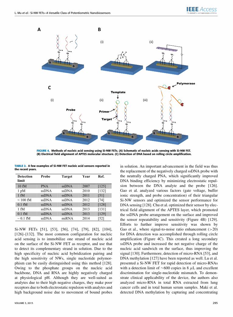
FIGURE 4. Methods of nucleic acid sensing using Si-NW FETs. (A) Schematic of nucleic acids sensing with Si-NW FET.(B) Electrical field alignment of APTES molecular structure. (C) Detection of DNA based on rolling circle amplification.
TABLE 2. A few examples of Si-NW FET nucleic acid sensors reported inthe recent years.
Si-NW FETs [51], [53], [56], [74], [79], [82], [104],[126]–[132]. The most common configuration for nucleicacid sensing is to immobilize one strand of nucleic acidon the surface of the Si-NW FET as receptor, and use thatto detect its complementary strand in solution. Due to thehigh specificity of nucleic acid hybridization pairing andthe high sensitivity of NWs, single nucleotide polymor-phism can be easily distinguished using this method [128].Owing to the phosphate groups on the nucleic acidbackbone, DNA and RNA are highly negatively chargedat physiological pH. Although they are well-suited asanalytes due to their high negative charges, they make poorreceptors due to both electrostatic repulsion with analytes andhigh background noise due to movement of bound probes
in solution. An important advancement in the field was thusthe replacement of the negatively charged ssDNA probe withthe neutrally charged PNA, which significantly improvedDNA binding efficiency by minimizing electrostatic repul-sion between the DNA analyte and the probe [126].Gao et al. analyzed various factors (gate voltage, bufferionic strength, and probe concentration) of their triangularSi-NW sensors and optimized the sensor performance forDNA sensing [128]. Chu et al. optimized their sensor by elec-trical field alignment of the APTES layer, which promotedthe ssDNA probe arrangement on the surface and improvedthe sensor repeatability and sensitivity (Figure 4B) [129].Efforts to further improve sensitivity was shown byGao et al., where signal-to-noise ratio enhancement (>20)for DNA detection was accomplished through rolling circleamplification (Figure 4C). This created a long secondaryssDNA probe and increased the net negative charge of thenucleic acid sandwich on the surface, thus improving thesignal [130]. Furthermore, detection of micro-RNA [53], andDNA methylation [127] have been reported as well. Lu et al.presented a Si-NW FET for rapid detection of micro-RNAswith a detection limit of ∼600 copies in 8 µL and excellentdiscrimination for single-nucleotide mismatch. To demon-strate clinical applicability of the device, the authors alsoanalyzed micro-RNA in total RNA extracted from lungcancer cells and in total human serum samples. Maki et al.detected DNA methylation by capturing and concentrating
VOLUME 3, 2015 295
L. Mu et al.: Si-NW FETs—A Versatile Class of Potentiometric Nanobiosensors
target DNA using magnetic beads, then testing the DNAusing NW-FET functionalized with anti-5-methylcytosinemolecule, which can capture methylated DNA. They wereable to detect methylated DNA down to 2.5 × 10⁻¹⁹ molin 0.25 µL of concentrated solution. Nucleic acid sensinghas also proven very useful in identification and detection ofinfectious diseases. Zhang et al. demonstrated a Si-NW FETbased on PNA-DNA hybridization for sensitive detection ofDengue virus following RT-PCR amplification of a definingfragment in the capsid region [56]. Kao et al. designed anintegrated microfluidic platform with Si-NW biosensors anda PCRmodule to detect the H1N1 2009 virus strain versus theseasonal influenza strain [104]. The PCR amplified nucleicacid products are directly flown downstream to be detectedon the NWs.
Besides concentration quantification, affinity based detec-tion (e.g. measuring receptor-analyte affinities and bindingkinetics) has also been demonstrated by Si-NW FETs forDNA hybridizations [86] and protein-DNA interactions [82].De et al. used a differential Si-NW setup to determine theequilibrium association constant of a 15-mer DNA to itscomplementary probe. The differential setup allowed for a30× reduction in drift. Duan et al. determined the equilibriumdissociation constant (KD ∼ 10−7 M) between the HMGB1protein and its ligand DNA. The real-time nature of theresponse allows kon and koff to be determined from the asso-ciation and dissociation curves, respectively. To show thatthe NW FETs can be applied to measure molecules across awide range of affinities, the same setup was used to determinethe dissociation constant of the biotin-streptavidin interaction(KD ∼ 10−14 M).Large-scale Si nanoFET sensor arrays for nucleic acid
detection could provide useful applications in detection ofinfectious agents from cellular extracts, gene expressionprofiling and sequencing.
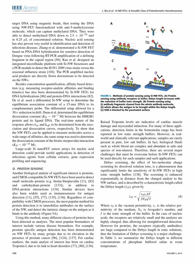
D. PROTEIN SENSINGAnother biological analyte of significant interest is proteins,and CMOS-compatible Si-NWFETs have been used to detectsmall molecule–protein (e.g. biotin-Streptavidin [11], [82]and carbohydrate-protein [133]), in addition toDNA-protein interactions [134]. Similar devices havealso been widely used as immunosensors for antigendetection [11], [55], [77], [135], [136]. Regardless of com-patibility with CMOS processes, the most popular method forprotein detection is to immobilize antibodies on the surfaceof the NW, and detect the intrinsic charge on the antigen as itbinds to the antibody (Figure 5A).
Using this method, many different classes of proteins havebeen detected as analytes. The most popular biomarkers ofinterest include various disease biomarkers. For example,prostate specific antigen detection has been demonstratedon NW FETs by many groups due to its elevation in thepresence of prostate cancer [96], [124], [137]. For cardiacmarkers, the main analyte of interest has been on cardiacTroponin I, due to its link to heart disorders [77], [80], [136].
FIGURE 5. Methods of protein sensing using Si-NW FETs. (A) Proteinsensing using antibody receptors in buffer, Debye length increases withthe reduction of buffer ionic strength. (B) Protein sensing using(i) antibody fragments cleaved from the whole antibody molecule,(ii) which allows the antigen to be brought within the Debye length.(C) NSB is blocked by the passivated surface.
Raised Troponin levels are indicative of cardiac muscledamage and myocardial infarction. For many of these appli-cations, detection limits in the femtomolar range has beenreported in low ionic strength buffers. However, in real-world and clinically relevant applications, samples are rarelypresent in pure, low salt buffers. In fact, biological fluidssuch as whole blood are complex and abundant in salts andspecies of non-interest. Therefore, there are several majorchallenges that must be overcome before Si-NW FETs canbe used directly for such samples and such applications.
Debye screening, the effect of bio-molecular chargescreening by dissolved solution ions, is a phenomenon thatsignificantly limits the sensitivity of Si-NW FETs in highionic strength buffers [138]. The screening is enhancedexponentially in distance from the charged analyte to theNW surface, and is described by a characteristic length calledthe Debye length (λD), given by
λD =
√ε0εrkT2NAq2I
(8)
Where ε0 is the vacuum permittivity, εr is the relative per-mittivity of the medium, NA is Avogadro’s number, andI is the ionic strength of the buffer. In the case of nucleicacids, the receptors are relatively small and the analytes arehighly charged, thus allowing for straightforward detection.However for proteins, the receptors (typically antibodies)are large compared to the Debye length in ionic solutions,thus the limitation of Debye screening is a major challenge.In Table 3, we summarize the Debye length in differentconcentrations of phosphate buffered saline at roomtemperature.
296 VOLUME 3, 2015
L. Mu et al.: Si-NW FETs—A Versatile Class of Potentiometric Nanobiosensors
TABLE 3. Summary of Debye lengths for various ionic strength solutions.
One can see that a solution to the issue is thereduction of buffer ionic strength, which will extend theDebye length. However, lowering the ionic strength requirescomplex desalting procedures, and may affect the stabilityand activity of various biological species. So far, the majorityof the work in this area has been done with the protein ofinterest spiked into prepared low salt buffers or desalted bio-logical fluids, and careful tuning of the buffer ionic strength isrequired [62], [133], [135]. An alternative method to reducingthe ionic strength is to bring the antigen within theDebye length, which has been successfully demonstratedon bottom up NWs. A way to achieve this is to replacethe large probe proteins with antibody fragments [80] oraptamers [139], which are relatively small and allow anti-gen binding to be detectable in physiological conditions.Elnathan et al. cleaved antibodies to obtain Fab portions, andused the fragments to sense troponin in high ionic strengthsolutions (Figure 5B). Using a moderate surface coverageof Fab fragments, cardiac troponin I was detected to a limitof <2 pM in 1× PBS [80]. Another way to bring antigenswithin the Debye length is to increase the Debye length itself.Recently, Gao et al. proposed a potential method for detectingproteins in high ionic strength solutions by incorporating aporous and biomolecule-permeable polyethylene glycol layeron the surface of the NW device [140]. The functionalizedpolymer layer increases the Debye screening lengthimmediately adjacent to the device surface, and alloweda concentration dependent response to be obtained forPSA concentrations from 10-1000 nM.
Another important issue that must be overcome beforeSi-NW FETs can be used to directly detect biomarkersfrom the whole blood sample is the issue of nonspecificbinding (NSB). Early studies were mainly focused on thedetection of pure protein samples and only very limitedresearch work has been directed toward biomarker detec-tion directly from the blood or serum mainly because ofchallenges caused by protein NSB and complexity of themedia. Chang et al. demonstrated a simple solution bypassivation of the nanowire surface using Tween 20 to blockthe signal induced by NSB when performing active measure-ment in whole blood (Figure 5C) [141]. An approach thatsimultaneously addresses the Debye length problem andNSBhas been reported by integrating a microfluidic filter chipwith Si-NW FETs to achieve target biomarkers adsorption,separation and elution, which is subsequently detected bySi-NW FETs. This strategy is quite promising as
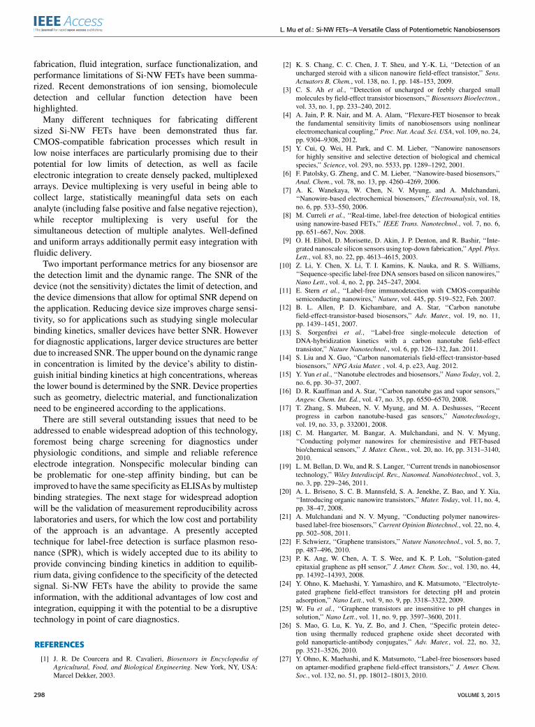
FIGURE 6. Methods of cell sensing using Si-NW FETs. (A) A bottom-upfabricated NW FET is inserted into a cell to record intracellular signals.(B) Detection of cellular activation via pH change. (C) Simultaneousdetection of multiple cytokines with a dually functionalized Si-NW chip.
a point-of-care clinical diagnostics tool for whole bloodsamples (e.g. collected by a finger prick) [124].
E. CELL SENSINGMicro/nanofabricated devices for the measurements ofcellular metabolism e.g., pH change, gas exchange(O2, CO2), ion concentration, redox potential, and intra-cellular/extracellular potential are rapidly growing researchfields [142], [143]. However, the negative effects of thelarger devices on the cell proliferation and cytotoxicity andmeasurement repeatability are major challenges. Due to theirrelatively small size and footprint, NWs have the advantageof being minimally invasive towards the cell and are capabledetection of at the single cell level. Both intracellular andextracellular activities have been recorded using Si-NWs andNW arrays. One special application of recording intracellularsignals by penetration cell membranes has been achievedby bottom-up fabricated 3D-NW FETs which is rather chal-lenging for top-down fabrication (Figure 6A) [144], [145].In extracellular applications, both single Si-NW and NWarrays have been applied for the detection of extracellularbioelectricity from neurons and cardiomyocytes, detection ofcellular activation via pH change (Figure 6B), simultaneousdetection of multiple cytokines in response to various stimulion one chip (Figure 6C), and determination of secretionkinetics of cytokines [55], [64], [75], [146], [147].Extracellular cell sensing is an important application ofCMOS-compatible NW-FETs, since the mass production ofsuch devices can facilitate the monitoring of static statesand/or dynamic evolution of biological process or reactionsindependently and simultaneously.
V. LIMITATIONS AND SUMMARYIn the past few years, Si-NW FETs have shown the abilityto detect a variety of biomolecules down to very lowconcentrations through potentiometric sensing. In thisreview, the operating principles, current methods for device
VOLUME 3, 2015 297
L. Mu et al.: Si-NW FETs—A Versatile Class of Potentiometric Nanobiosensors
fabrication, fluid integration, surface functionalization, andperformance limitations of Si-NW FETs have been summa-rized. Recent demonstrations of ion sensing, biomoleculedetection and cellular function detection have beenhighlighted.
Many different techniques for fabricating differentsized Si-NW FETs have been demonstrated thus far.CMOS-compatible fabrication processes which result inlow noise interfaces are particularly promising due to theirpotential for low limits of detection, as well as facileelectronic integration to create densely packed, multiplexedarrays. Device multiplexing is very useful in being able tocollect large, statistically meaningful data sets on eachanalyte (including false positive and false negative rejection),while receptor multiplexing is very useful for thesimultaneous detection of multiple analytes. Well-definedand uniform arrays additionally permit easy integration withfluidic delivery.
Two important performance metrics for any biosensor arethe detection limit and the dynamic range. The SNR of thedevice (not the sensitivity) dictates the limit of detection, andthe device dimensions that allow for optimal SNR depend onthe application. Reducing device size improves charge sensi-tivity, so for applications such as studying single molecularbinding kinetics, smaller devices have better SNR. Howeverfor diagnostic applications, larger device structures are betterdue to increased SNR. The upper bound on the dynamic rangein concentration is limited by the device’s ability to distin-guish initial binding kinetics at high concentrations, whereasthe lower bound is determined by the SNR. Device propertiessuch as geometry, dielectric material, and functionalizationneed to be engineered according to the applications.
There are still several outstanding issues that need to beaddressed to enable widespread adoption of this technology,foremost being charge screening for diagnostics underphysiologic conditions, and simple and reliable referenceelectrode integration. Nonspecific molecular binding canbe problematic for one-step affinity binding, but can beimproved to have the same specificity as ELISAs bymultistepbinding strategies. The next stage for widespread adoptionwill be the validation of measurement reproducibility acrosslaboratories and users, for which the low cost and portabilityof the approach is an advantage. A presently acceptedtechnique for label-free detection is surface plasmon reso-nance (SPR), which is widely accepted due to its ability toprovide convincing binding kinetics in addition to equilib-rium data, giving confidence to the specificity of the detectedsignal. Si-NW FETs have the ability to provide the sameinformation, with the additional advantages of low cost andintegration, equipping it with the potential to be a disruptivetechnology in point of care diagnostics.
REFERENCES
[1] J. R. De Courcera and R. Cavalieri, Biosensors in Encyclopedia ofAgricultural, Food, and Biological Engineering. New York, NY, USA:Marcel Dekker, 2003.
[2] K. S. Chang, C. C. Chen, J. T. Sheu, and Y.-K. Li, ‘‘Detection of anuncharged steroid with a silicon nanowire field-effect transistor,’’ Sens.Actuators B, Chem., vol. 138, no. 1, pp. 148–153, 2009.
[3] C. S. Ah et al., ‘‘Detection of uncharged or feebly charged smallmolecules by field-effect transistor biosensors,’’ Biosensors Bioelectron.,vol. 33, no. 1, pp. 233–240, 2012.
[4] A. Jain, P. R. Nair, and M. A. Alam, ‘‘Flexure-FET biosensor to breakthe fundamental sensitivity limits of nanobiosensors using nonlinearelectromechanical coupling,’’ Proc. Nat. Acad. Sci. USA, vol. 109, no. 24,pp. 9304–9308, 2012.
[5] Y. Cui, Q. Wei, H. Park, and C. M. Lieber, ‘‘Nanowire nanosensorsfor highly sensitive and selective detection of biological and chemicalspecies,’’ Science, vol. 293, no. 5533, pp. 1289–1292, 2001.
[6] F. Patolsky, G. Zheng, and C. M. Lieber, ‘‘Nanowire-based biosensors,’’Anal. Chem., vol. 78, no. 13, pp. 4260–4269, 2006.
[7] A. K. Wanekaya, W. Chen, N. V. Myung, and A. Mulchandani,‘‘Nanowire-based electrochemical biosensors,’’ Electroanalysis, vol. 18,no. 6, pp. 533–550, 2006.
[8] M. Curreli et al., ‘‘Real-time, label-free detection of biological entitiesusing nanowire-based FETs,’’ IEEE Trans. Nanotechnol., vol. 7, no. 6,pp. 651–667, Nov. 2008.
[9] O. H. Elibol, D. Morisette, D. Akin, J. P. Denton, and R. Bashir, ‘‘Inte-grated nanoscale silicon sensors using top-down fabrication,’’ Appl. Phys.Lett., vol. 83, no. 22, pp. 4613–4615, 2003.
[10] Z. Li, Y. Chen, X. Li, T. I. Kamins, K. Nauka, and R. S. Williams,‘‘Sequence-specific label-free DNA sensors based on silicon nanowires,’’Nano Lett., vol. 4, no. 2, pp. 245–247, 2004.
[11] E. Stern et al., ‘‘Label-free immunodetection with CMOS-compatiblesemiconducting nanowires,’’ Nature, vol. 445, pp. 519–522, Feb. 2007.
[12] B. L. Allen, P. D. Kichambare, and A. Star, ‘‘Carbon nanotubefield-effect-transistor-based biosensors,’’ Adv. Mater., vol. 19, no. 11,pp. 1439–1451, 2007.
[13] S. Sorgenfrei et al., ‘‘Label-free single-molecule detection ofDNA-hybridization kinetics with a carbon nanotube field-effecttransistor,’’ Nature Nanotechnol., vol. 6, pp. 126–132, Jan. 2011.
[14] S. Liu and X. Guo, ‘‘Carbon nanomaterials field-effect-transistor-basedbiosensors,’’ NPG Asia Mater. , vol. 4, p. e23, Aug. 2012.
[15] Y. Yun et al., ‘‘Nanotube electrodes and biosensors,’’ Nano Today, vol. 2,no. 6, pp. 30–37, 2007.
[16] D. R. Kauffman and A. Star, ‘‘Carbon nanotube gas and vapor sensors,’’Angew. Chem. Int. Ed., vol. 47, no. 35, pp. 6550–6570, 2008.
[17] T. Zhang, S. Mubeen, N. V. Myung, and M. A. Deshusses, ‘‘Recentprogress in carbon nanotube-based gas sensors,’’ Nanotechnology,vol. 19, no. 33, p. 332001, 2008.
[18] C. M. Hangarter, M. Bangar, A. Mulchandani, and N. V. Myung,‘‘Conducting polymer nanowires for chemiresistive and FET-basedbio/chemical sensors,’’ J. Mater. Chem., vol. 20, no. 16, pp. 3131–3140,2010.
[19] L. M. Bellan, D. Wu, and R. S. Langer, ‘‘Current trends in nanobiosensortechnology,’’Wiley Interdiscipl. Rev., Nanomed. Nanobiotechnol., vol. 3,no. 3, pp. 229–246, 2011.
[20] A. L. Briseno, S. C. B. Mannsfeld, S. A. Jenekhe, Z. Bao, and Y. Xia,‘‘Introducing organic nanowire transistors,’’Mater. Today, vol. 11, no. 4,pp. 38–47, 2008.
[21] A. Mulchandani and N. V. Myung, ‘‘Conducting polymer nanowires-based label-free biosensors,’’ Current Opinion Biotechnol., vol. 22, no. 4,pp. 502–508, 2011.
[23] P. K. Ang, W. Chen, A. T. S. Wee, and K. P. Loh, ‘‘Solution-gatedepitaxial graphene as pH sensor,’’ J. Amer. Chem. Soc., vol. 130, no. 44,pp. 14392–14393, 2008.
[24] Y. Ohno, K. Maehashi, Y. Yamashiro, and K. Matsumoto, ‘‘Electrolyte-gated graphene field-effect transistors for detecting pH and proteinadsorption,’’ Nano Lett., vol. 9, no. 9, pp. 3318–3322, 2009.
[25] W. Fu et al., ‘‘Graphene transistors are insensitive to pH changes insolution,’’ Nano Lett., vol. 11, no. 9, pp. 3597–3600, 2011.
[26] S. Mao, G. Lu, K. Yu, Z. Bo, and J. Chen, ‘‘Specific protein detec-tion using thermally reduced graphene oxide sheet decorated withgold nanoparticle-antibody conjugates,’’ Adv. Mater., vol. 22, no. 32,pp. 3521–3526, 2010.
[27] Y. Ohno, K. Maehashi, and K. Matsumoto, ‘‘Label-free biosensors basedon aptamer-modified graphene field-effect transistors,’’ J. Amer. Chem.Soc., vol. 132, no. 51, pp. 18012–18013, 2010.
298 VOLUME 3, 2015
L. Mu et al.: Si-NW FETs—A Versatile Class of Potentiometric Nanobiosensors
[28] N. Mohanty and V. Berry, ‘‘Graphene-based single-bacterium resolutionbiodevice and DNA transistor: Interfacing graphene derivatives withnanoscale and microscale biocomponents,’’ Nano Lett., vol. 8, no. 12,pp. 4469–4476, 2008.
[29] X. Dong, Y. Shi, W. Huang, P. Chen, and L.-J. Li, ‘‘Electrical detec-tion of DNA hybridization with single-base specificity using transistorsbased on CVD-grown graphene sheets,’’ Adv. Mater., vol. 22, no. 14,pp. 1649–1653, 2010.
[30] B. Cai, S. Wang, L. Huang, Y. Ning, Z. Zhang, and G.-J. Zhang, ‘‘Ultra-sensitive label-free detection of PNA–DNA hybridization by reducedgraphene oxide field-effect transistor biosensor,’’ ACS Nano, vol. 8, no. 3,pp. 2632–2638, 2014.
[31] Y. Huang, X. Dong, Y. Shi, C. M. Li, L.-J. Li, and P. Chen, ‘‘Nanoelec-tronic biosensors based on CVD grown graphene,’’ Nanoscale, vol. 2,no. 8, pp. 1485–1488, 2010.
[32] T. Cohen-Karni, Q. Qing, Q. Li, Y. Fang, and C. M. Lieber, ‘‘Grapheneand nanowire transistors for cellular interfaces and electrical recording,’’Nano Lett., vol. 10, no. 3, pp. 1098–1102, 2010.
[33] D. Sarkar, W. Liu, X. Xie, A. C. Anselmo, S. Mitragotri, and K. Banerjee,‘‘MoS2 field-effect transistor for next-generation label-free biosensors,’’ACS Nano, vol. 8, no. 4, pp. 3992–4003, 2014.
[34] G. Jágerszki, Á. Takács, I. Bitter, and R. E. Gyurcsányi, ‘‘Solid-stateion channels for potentiometric sensing,’’ Angew. Chem., vol. 123, no. 7,pp. 1694–1697, 2011.
[35] T. Yin and W. Qin, ‘‘Applications of nanomaterials in potentiometricsensors,’’ TrAC Trends Anal. Chem., vol. 51, pp. 79–86, Nov. 2013.
[36] J. Ampurdanés, G. A. Crespo, A. Maroto, M. A. Sarmentero, P. Ballester,and F. X. Rius, ‘‘Determination of choline and derivatives with a solid-contact ion-selective electrode based on octaamide cavitand and carbonnanotubes,’’ Biosensors Bioelectron., vol. 25, no. 2, pp. 344–349, 2009.
[37] G. A. Crespo, D. Gugsa, S. Macho, and F. X. Rius, ‘‘Solid-contactpH-selective electrode using multi-walled carbon nanotubes,’’ Anal.Bioanal. Chem., vol. 395, no. 7, pp. 2371–2376, 2009.
[38] E. Jaworska, M. Wójcik, A. Kisiel, J. Mieczkowski, and A. Michalska,‘‘Gold nanoparticles solid contact for ion-selective electrodes of highlystable potential readings,’’ Talanta, vol. 85, no. 4, pp. 1986–1989, 2011.
[39] J. L. Arlett, E. B. Myers, and M. L. Roukes, ‘‘Comparative advantagesof mechanical biosensors,’’ Nature Nanotechnol., vol. 6, pp. 203–215,Mar. 2011.
[40] R. S. Wagner and W. C. Ellis, ‘‘Vapor-liquid-solid mechanism of singlecrystal growth,’’ Appl. Phys. Lett., vol. 4, no. 5, pp. 89–90, 1964.
[41] Y. Huang, X. Duan, Q.Wei, and C.M. Lieber, ‘‘Directed assembly of one-dimensional nanostructures into functional networks,’’ Science, vol. 291,no. 5504, pp. 630–633, 2001.
[42] D. Whang, S. Jin, Y. Wu, and C. M. Lieber, ‘‘Large-scale hierarchicalorganization of nanowire arrays for integrated nanosystems,’’ Nano Lett.,vol. 3, no. 9, pp. 1255–1259, 2003.
[43] S. Jin, D. Whang, M. C. McAlpine, R. S. Friedman, Y. Wu, andC. M. Lieber, ‘‘Scalable interconnection and integration of nanowiredevices without registration,’’Nano Lett., vol. 4, no. 5, pp. 915–919, 2004.
[44] G. Yu, A. Cao, and C. M. Lieber, ‘‘Large-area blown bubble films ofaligned nanowires and carbon nanotubes,’’ Nature Nanotechnol., vol. 2,pp. 372–377, May 2007.
[45] Z. Fan et al., ‘‘Wafer-scale assembly of highly ordered semiconductornanowire arrays by contact printing,’’ Nano Lett., vol. 8, no. 1, pp. 20–25,2008.
[46] L. Dong et al., ‘‘Dielectrophoretically controlled fabrication of single-crystal nickel silicide nanowire interconnects,’’ Nano Lett., vol. 5, no. 10,pp. 2112–2115, 2005.
[47] S. Raychaudhuri, S. A. Dayeh, D. Wang, and E. T. Yu, ‘‘Precise semicon-ductor nanowire placement through dielectrophoresis,’’Nano Lett., vol. 9,no. 6, pp. 2260–2266, 2009.
[48] E. M. Freer, O. Grachev, X. Duan, S. Martin, and D. P. Stumbo, ‘‘High-yield self-limiting single-nanowire assembly with dielectrophoresis,’’Nature Nanotechnol., vol. 5, pp. 525–530, Jun. 2010.
[49] I. Park, Z. Li, A. P. Pisano, and R. S.Williams, ‘‘Top-down fabricated sili-con nanowire sensors for real-time chemical detection,’’Nanotechnology,vol. 21, no. 1, p. 015501, 2010.
[50] A. Tarasov et al., ‘‘True reference nanosensor realized with siliconnanowires,’’ Langmuir, vol. 28, no. 25, pp. 9899–9905, 2012.
[51] A. Gao et al., ‘‘Silicon-nanowire-based CMOS-compatible field-effecttransistor nanosensors for ultrasensitive electrical detection of nucleicacids,’’ Nano Lett., vol. 11, no. 9, pp. 3974–3978, 2011.
[52] N. Lu et al., ‘‘Ultra-sensitive nucleic acids detection with electricalnanosensors based on CMOS-compatible silicon nanowire field-effecttransistors,’’ Methods, vol. 63, no. 3, pp. 212–218, 2013.
[53] N. Lu et al., ‘‘CMOS-compatible silicon nanowire field-effect transistorsfor ultrasensitive and label-free microRNAs sensing,’’ Small, vol. 10,no. 10, pp. 2022–2028, 2014.
[54] R. Juhasz, N. Elfström, and J. Linnros, ‘‘Controlled fabrication of siliconnanowires by electron beam lithography and electrochemical size reduc-tion,’’ Nano Lett., vol. 5, no. 2, pp. 275–280, 2005.
[55] T.-S. Pui, A. Agarwal, F. Ye, Z.-Q. Tou, Y. Huang, and P. Chen,‘‘Ultra-sensitive detection of adipocytokines with CMOS-compatiblesilicon nanowire arrays,’’ Nanoscale, vol. 1, no. 1, pp. 159–163,2009.
[56] G.-J. Zhang et al., ‘‘Silicon nanowire biosensor for highly sensitive andrapid detection of dengue virus,’’ Sens. Actuators B, Chem., vol. 146,no. 1, pp. 138–144, 2010.
[57] S. Chen, J. G. Bomer, W. G. van der Wiel, E. T. Carlen, andA. van den Berg, ‘‘Top-down fabrication of sub-30 nm monocrystallinesilicon nanowires using conventional microfabrication,’’ ACS Nano,vol. 3, no. 11, pp. 3485–3492, 2009.
[58] N. K. Rajan, D. A. Routenberg, J. Chen, and M. A. Reed, ‘‘1/f noise ofsilicon nanowire BioFETs,’’ IEEE Electron Device Lett., vol. 31, no. 6,pp. 615–617, Jun. 2010.
[59] B. Reddy, Jr., et al., ‘‘High-k dielectric Al2O3 nanowire and nanoplatefield effect sensors for improved pH sensing,’’ Biomed. Microdevices,vol. 13, no. 2, pp. 335–344, 2011.
[60] N. Elfström, A. E. Karlström, and J. Linnros, ‘‘Silicon nanoribbonsfor electrical detection of biomolecules,’’ Nano Lett., vol. 8, no. 3,pp. 945–949, Mar. 2008.
[61] L. Mu, I. A. Droujinine, N. K. Rajan, S. D. Sawtelle, and M. A. Reed,‘‘Direct, rapid, and label-free detection of enzyme-substrate interactionsin physiological buffers using CMOS-compatible nanoribbon sensors,’’Nano Lett., vol. 14, no. 9, pp. 5315–5322, 2014.
[62] M. M. Hakim et al., ‘‘Thin film polycrystalline silicon nanowire biosen-sors,’’ Nano Lett., vol. 12, no. 4, pp. 1868–1872, 2012.
[63] C.-H. Lin, C.-H. Hung, C.-Y. Hsiao, H.-C. Lin, F.-H. Ko, andY.-S. Yang, ‘‘Poly-silicon nanowire field-effect transistor for ultrasen-sitive and label-free detection of pathogenic avian influenza DNA,’’Biosensors Bioelectron., vol. 24, no. 10, pp. 3019–3024, 2009.
[64] T. S. Pui, A. Agarwal, F. Ye, N. Balasubramanian, and P. Chen, ‘‘CMOS-compatible nanowire sensor arrays for detection of cellular bioelectric-ity,’’ Small, vol. 5, no. 2, pp. 208–212, 2009.
[65] S. Rigante et al., ‘‘Sensing with advanced computing technology: Finfield effect transistors with high-k gate stack on bulk silicon,’’ ACS Nano,2015.
[66] A. Gao, N. Lu, P. Dai, C. Fan, Y. Wang, and T. Li, ‘‘Direct ultrasensitiveelectrical detection of prostate cancer biomarkers with CMOS-compatiblen- and p-type silicon nanowire sensor arrays,’’ Nanoscale, vol. 6, no. 21,pp. 13036–13042, 2014.
[67] M.-C. Chen et al., ‘‘A CMOS-compatible poly-Si nanowire device withhybrid sensor/memory characteristics for system-on-chip applications,’’Sensors, vol. 12, no. 4, pp. 3952–3963, 2012.
[68] C. W. Huang et al., ‘‘A CMOS wireless biomolecular sensing system-on-chip based on polysilicon nanowire technology,’’ Lab Chip, vol. 13,no. 22, pp. 4451–4459, 2013.
[69] A. Vacic, J. M. Criscione, E. Stern, N. K. Rajan, T. Fahmy, andM. A. Reed, ‘‘Calibration methods for silicon nanowire BioFETs,’’in Proc. Int. Conf. Microelectron. Test Struct. (ICMTS), Mar. 2014,pp. 203–206.
[70] H.-J. Jang, M.-S. Kim, and W.-J. Cho, ‘‘Development of engineeredsensingmembranes for field-effect ion-sensitive devices based on stackedhigh-κ dielectric layers,’’ IEEE Electron Device Lett., vol. 32, no. 7,pp. 973–975, Jul. 2011.
[71] T.-E. Bae, H.-J. Jang, J.-H. Yang, and W.-J. Cho, ‘‘High performance ofsilicon nanowire-based biosensors using a high-k stacked sensing thinfilm,’’ ACS Appl. Mater. Interf., vol. 5, no. 11, pp. 5214–5218, 2013.
[72] S. Chen, J. G. Bomer, E. T. Carlen, and A. van den Berg, ‘‘Al2O3/siliconnanoISFET with near ideal Nernstian response,’’ Nano Lett., vol. 11,no. 6, pp. 2334–2341, 2011.
[73] S. Zafar, C. D’Emic, A. Afzali, B. Fletcher, Y. Zhu, and T. Ning, ‘‘Opti-mization of pH sensing using silicon nanowire field effect transistors withHfO2 as the sensing surface,’’Nanotechnology, vol. 22, no. 40, p. 405501,2011.
VOLUME 3, 2015 299
L. Mu et al.: Si-NW FETs—A Versatile Class of Potentiometric Nanobiosensors
[74] B. R. Dorvel et al., ‘‘Silicon nanowires with high-k hafnium oxidedielectrics for sensitive detection of small nucleic acid oligomers,’’ ACSNano, vol. 6, no. 7, pp. 6150–6164, 2012.
[75] E. Stern, E. R. Steenblock, M. A. Reed, and T. M. Fahmy, ‘‘Label-freeelectronic detection of the antigen-specific T-cell immune response,’’Nano Lett., vol. 8, no. 10, pp. 3310–3314, 2008.
[76] A. De, J. van Nieuwkasteele, E. T. Carlen, and A. van den Berg, ‘‘Inte-grated label-free silicon nanowire sensor arrays for (bio)chemical analy-sis,’’ Analyst, vol. 138, no. 11, pp. 3221–3229, 2013.
[77] J. H. Chua, R.-E. Chee, A. Agarwal, S. M. Wong, and G.-J. Zhang,‘‘Label-free electrical detection of cardiac biomarker with comple-mentary metal-oxide semiconductor-compatible silicon nanowire sensorarrays,’’ Anal. Chem., vol. 81, no. 15, pp. 6266–6271, 2009.
[78] D. R. Kim, C. H. Lee, and X. Zheng, ‘‘Probing flow velocity with siliconnanowire sensors,’’ Nano Lett., vol. 9, no. 5, pp. 1984–1988, 2009.
[79] M. Chiesa et al., ‘‘Detection of the early stage of recombinationalDNA repair by silicon nanowire transistors,’’ Nano Lett., vol. 12, no. 3,pp. 1275–1281, 2012.
[80] R. Elnathan et al., ‘‘Biorecognition layer engineering: Overcomingscreening limitations of nanowire-based FET devices,’’ Nano Lett.,vol. 12, no. 10, pp. 5245–5254, 2012.
[82] X. Duan, Y. Li, N. K. Rajan, D. A. Routenberg, Y.Modis, andM. A. Reed,‘‘Quantification of the affinities and kinetics of protein interactions usingsilicon nanowire biosensors,’’ Nature Nanotechnol., vol. 7, pp. 401–407,May 2012.
[83] A. Tarasov et al., ‘‘Understanding the electrolyte background for bio-chemical sensing with ion-sensitive field-effect transistors,’’ ACS Nano,vol. 6, no. 10, pp. 9291–9298, 2012.
[84] M. Wipf et al., ‘‘Selective sodium sensing with gold-coated siliconnanowire field-effect transistors in a differential setup,’’ACSNano, vol. 7,no. 7, pp. 5978–5983, 2013.
[85] S. Kim et al., ‘‘Silicon nanowire ion sensitive field effect transistor withintegrated Ag/AgCl electrode: pH sensing and noise characteristics,’’Analyst, vol. 136, no. 23, pp. 5012–5016, 2011.
[86] Y. L. Bunimovich, Y. S. Shin, W.-S. Yeo, M. Amori, G. Kwong, andJ. R. Heath, ‘‘Quantitative real-time measurements of DNA hybridizationwith alkylated nonoxidized silicon nanowires in electrolyte solution,’’J. Amer. Chem. Soc., vol. 128, no. 50, pp. 16323–16331, 2006.
[87] X. Duan, N. K. Rajan, M. H. Izadi, and M. A. Reed, ‘‘Complemen-tary metal oxide semiconductor-compatible silicon nanowire biofield-effect transistors as affinity biosensors,’’ Nanomedicine, vol. 8, no. 11,pp. 1839–1851, 2013.
[88] L. C. P. M. de Smet, D. Ullien, E. J. R. Sudhölter, andM. Mescher, Organic Surface Modification of Silicon Nanowire-BasedSensor Devices. Rijeka, Croatia: InTech, 2011.
[89] B. Dorvel, B. Reddy, Jr., and R. Bashir, ‘‘Effect of biointerfacing linkerchemistries on the sensitivity of silicon nanowires for protein detection,’’Anal. Chem., vol. 85, no. 20, pp. 9493–9500, Oct. 2013.
[90] S.-P. Lin, T.-Y. Chi, T.-Y. Lai, and M.-C. Liu, ‘‘The effect of variedfunctional biointerfaces on the sensitivity of silicon nanowire MOSFET,’’in Proc. IEEE EMBS Conf. Biomed. Eng. Sci. (IECBES), Dec. 2012,pp. 162–166.
[91] B. Dorvel et al., ‘‘Vapor-phase deposition of monofunctional alkoxysi-lanes for sub-nanometer-level biointerfacing on silicon oxide surfaces,’’Adv. Funct. Mater., vol. 20, no. 1, pp. 87–95, 2010.
[92] R. Ermanok, O. Assad, K. Zigelboim, B. Wang, and H. Haick, ‘‘Dis-criminative power of chemically sensitive silicon nanowire field effecttransistors to volatile organic compounds,’’ ACS Appl. Mater. Interf.,vol. 5, no. 21, pp. 11172–11183, 2013.
[93] X. Duan, N. K. Rajan, D. A. Routenberg, J. Huskens, and M. A. Reed,‘‘Regenerative electronic biosensors using supramolecular approaches,’’ACS Nano, vol. 7, no. 5, pp. 4014–4021, 2013.
[94] X. Duan et al., ‘‘Functionalized polyelectrolytes assembling on nano-BioFETs for biosensing applications,’’ Adv. Funct. Mater., vol. 25, no. 15,pp. 2279–2286, 2015.
[95] Y. Engel, R. Elnathan, A. Pevzner, G. Davidi, E. Flaxer, and F. Patolsky,‘‘Supersensitive detection of explosives by silicon nanowire arrays,’’Angew. Chem. Int. Ed., vol. 49, no. 38, pp. 6830–6835, 2010.
[96] G. Zheng, F. Patolsky, Y. Cui, W. U. Wang, and C. M. Lieber, ‘‘Mul-tiplexed electrical detection of cancer markers with nanowire sensorarrays,’’ Nature Biotechnol., vol. 23, pp. 1294–1301, Sep. 2005.
[97] G.-J. Zhang, Z. H. H. Luo, M. J. Huang, J. J. Ang, T. G. Kang, andH. Ji, ‘‘An integrated chip for rapid, sensitive, and multiplexed detectionof cardiac biomarkers from fingerprick blood,’’ Biosensors Bioelectron.,vol. 28, no. 1, pp. 459–463, 2011.
[98] I. Park, Z. Li, A. P. Pisano, and R. S. Williams, ‘‘Selective surfacefunctionalization of silicon nanowires via nanoscale Joule heating,’’NanoLett., vol. 7, no. 10, pp. 3106–3111, 2007.
[99] E. Stern et al., ‘‘Electropolymerization on microelectrodes: Function-alization technique for selective protein and DNA conjugation,’’ Anal.Chem., vol. 78, no. 18, pp. 6340–6346, 2006.
[100] Y. L. Bunimovich, G. Ge, K. C. Beverly, R. S. Ries, L. Hood,and J. R. Heath, ‘‘Electrochemically programmed, spatially selec-tive biofunctionalization of silicon wires,’’ Langmuir, vol. 20, no. 4,pp. 10630–10638, 2004.
[101] J.-H. Lim, D. S. Ginger, K.-B. Lee, J. Heo, J.-M. Nam, and C. A. Mirkin,‘‘Direct-write dip-pen nanolithography of proteins on modified siliconoxide surfaces,’’ Angew. Chem. Int. Ed., vol. 42, no. 20, pp. 2309–2312,May 2003.
[102] G.-J. Zhang et al., ‘‘Multiplexed detection of cardiac biomarkers in serumwith nanowire arrays using readout ASIC,’’ Biosensors Bioelectron.,vol. 35, no. 1, pp. 218–223, May 2012.
[103] A. Kim et al., ‘‘Direct label-free electrical immunodetection in humanserum using a flow-through-apparatus approach with integrated field-effect transistors,’’Biosensors Bioelectron., vol. 25, no. 7, pp. 1767–1773,Mar. 2010.
[104] L. T.-H. Kao et al., ‘‘Multiplexed detection and differentiation of theDNA strains for influenza A (H1N1 2009) using a silicon-based microflu-idic system,’’ Biosensors Bioelectron., vol. 26, no. 5, pp. 2006–2011,Jan. 2011.
[105] K. J. Albert et al., ‘‘Cross-reactive chemical sensor arrays,’’ Chem. Rev.,vol. 100, no. 7, pp. 2595–2626, 2000.
[106] A. Cao, E. J. R. Sudhölter, and L. C. P. M. de Smet, ‘‘Siliconnanowire-based devices for gas-phase sensing,’’ Sensors, vol. 14, no. 1,pp. 245–271, Jan. 2013.
[107] B. Wang, J. C. Cancilla, J. S. Torrecilla, and H. Haick, ‘‘Artificial sensingintelligence with silicon nanowires for ultraselective detection in the gasphase,’’ Nano Lett., vol. 14, no. 2, pp. 933–938, Jan. 2014.
[108] P. R. Nair and M. A. Alam, ‘‘Performance limits of nanobiosensors,’’Appl. Phys. Lett., vol. 88, no. 3, p. 233120, Jun. 2006.
[109] N. K. Rajan, X. Duan, and M. A. Reed, ‘‘Performance limitations fornanowire/nanoribbon biosensors,’’ Nanomed. Nanobiotechnol., vol. 5,no. 6, pp. 629–645, Nov. 2013.
[110] R. Jayaraman and C. G. Sodini, ‘‘A 1/f noise technique to extract theoxide trap density near the conduction band edge of silicon,’’ IEEE Trans.Electron Devices, vol. 36, no. 8, pp. 1773–1782, Sep. 1989.
[111] N. K. Rajan, D. A. Routenberg, andM.A. Reed, ‘‘Optimal signal-to-noiseratio for silicon nanowire biochemical sensors,’’ Appl. Phys. Lett., vol. 98,no. 26, p. 264107, Jun. 2011.
[112] K. Bedner et al., ‘‘Investigation of the dominant 1/f noise sourcein silicon nanowire sensors,’’ Sens. Actuators B, Chem., vol. 191,pp. 270–275, Feb. 2014.
[113] N. K. Rajan, K. Brower, X. Duan, and M. A. Reed, ‘‘Limit of detection offield effect transistor biosensors: Effects of surface modification and sizedependence,’’ Appl. Phys. Lett., vol. 104, no. 8, p. 084106, Feb. 2014.
[114] V. S. Mahajan and P. Jarolim, ‘‘How to interpret elevated cardiac troponinlevels,’’ Circulation, vol. 124, no. 21, pp. 2350–2354, Nov. 2011.
[115] P. Bergveld, ‘‘Thirty years of ISFETOLOGY: What happened in the past30 years and what may happen in the next 30 years,’’ Sens. Actuators B,Chem., vol. 88, no. 1, pp. 1–20, Jan. 2003.
[116] X. T. Vu, R. Stockmann, B. Wolfrum, A. Offenhäusser, andS. Ingebrandt, ‘‘Fabrication and application of a microfluidic-embeddedsilicon nanowire biosensor chip,’’ Phys. Status Solidi A, vol. 207, no. 4,pp. 850–857, Apr. 2010.
[117] R. Tian, S. Regonda, J. Gao, Y. Liu, and W. Hu, ‘‘Ultrasensitive proteindetection using lithographically defined Si multi-nanowire field effecttransistors,’’ Lab Chip, vol. 11, no. 11, pp. 1952–1961, Apr. 2011.
[118] S. Choi, I. Park, Z. Hao, H.-Y. N. Holman, and A. P. Pisano, ‘‘Quantitativestudies of long-term stable, top-down fabricated silicon nanowire pHsensors,’’ Appl. Phys. A, vol. 107, no. 2, pp. 421–428, May 2012.
[119] X. P. A. Gao, G. Zheng, and C. M. Lieber, ‘‘Subthreshold regime has theoptimal sensitivity for nanowire FET biosensors,’’ Nano Lett., vol. 10,no. 2, pp. 547–552, Nov. 2009.
[120] O. Knopfmacher et al., ‘‘Nernst limit in dual-gated Si-nanowire FETsensors,’’ Nano Lett., vol. 10, no. 6, pp. 2268–2274, May 2010.
300 VOLUME 3, 2015
L. Mu et al.: Si-NW FETs—A Versatile Class of Potentiometric Nanobiosensors
[121] E. Stern et al., ‘‘A nanoelectronic enzyme-linked immunosorbent assayfor detection of proteins in physiological solutions,’’ Small, vol. 6, no. 2,pp. 232–238, Jan. 2010.
[122] L. Luo et al., ‘‘Silicon nanowire sensors for Hg2+ and Cd2+ ions,’’ Appl.Phys. Lett., vol. 94, no. 19, pp. 193101-1–193101-3, 2009.
[123] X. Bi, A. Agarwal, and K.-L. Yang, ‘‘Oligopeptide-modified sili-con nanowire arrays as multichannel metal ion sensors,’’ BiosensorsBioelectron., vol. 24, no. 11, pp. 3248–3251, Jul. 2009.
[124] E. Stern et al., ‘‘Label-free biomarker detection from whole blood,’’Nature Nanotechnol., vol. 5, no. 2, pp. 138–142, 2010.
[125] Z. Gao et al., ‘‘Silicon nanowire arrays for label-free detection of DNA,’’Anal. Chem., vol. 79, no. 9, pp. 3291–3297, Apr. 2007.
[126] A. Cattani-Scholz et al., ‘‘Organophosphonate-based PNA-functionalization of silicon nanowires for label-free DNA detection,’’ACS Nano, vol. 2, no. 8, pp. 1653–1660, Jul. 2008.
[127] W. C. Maki, N. N. Mishra, E. G. Cameron, B. Filanoski, S. K. Rastogi,and G. K. Maki, ‘‘Nanowire-transistor based ultra-sensitive DNA methy-lation detection,’’ Biosensors Bioelectron., vol. 23, no. 6, pp. 780–787,Jan. 2008.
[128] A. Gao et al., ‘‘Enhanced sensing of nucleic acids with siliconnanowire field effect transistor biosensors,’’ Nano Lett., vol. 12, no. 10,pp. 5262–5268, Sep. 2012.
[129] C.-J. Chu et al., ‘‘Improving nanowire sensing capability by electricalfield alignment of surface probing molecules,’’ Nano Lett., vol. 13, no. 6,pp. 2564–2569, May 2013.
[130] A. Gao et al., ‘‘Signal-to-noise ratio enhancement of silicon nanowiresbiosensor with rolling circle amplification,’’ Nano Lett., vol. 13, no. 9,pp. 4123–4130, Aug. 2013.
[131] G. Wenga, E. Jacques, A.-C. Salaün, R. Rogel, L. Pichon, andF. Geneste, ‘‘Step-gate polysilicon nanowires field effect transistorcompatible with CMOS technology for label-free DNA biosensor,’’Biosensors Bioelectron., vol. 40, no. 1, pp. 141–146, Feb. 2013.
[132] S.-W. Ryu et al., ‘‘Gold nanoparticle embedded silicon nanowirebiosensor for applications of label-free DNA detection,’’ BiosensorsBioelectron., vol. 25, no. 9, pp. 2182–2185, May 2010.
[133] G.-J. Zhang, M. J. Huang, J. J. Ang, Q. Yao, and Y. Ning, ‘‘Label-free detection of carbohydrate–protein interactions using nanoscale field-effect transistor biosensors,’’ Anal. Chem., vol. 85, no. 9, pp. 4392–4397,Apr. 2013.
[134] G.-J. Zhang et al., ‘‘Highly sensitive and reversible silicon nanowirebiosensor to study nuclear hormone receptor protein and responseelement DNA interactions,’’ Biosensors Bioelectron., vol. 26, no. 2,pp. 365–370, Oct. 2010.
[135] D. P. Tran et al., ‘‘Complementary metal oxide semiconductor compatiblesilicon nanowires-on-a-chip: Fabrication and preclinical validation for thedetection of a cancer prognostic protein marker in serum,’’ Anal. Chem.,vol. 87, no. 3, pp. 1662–1668, Feb. 2015.
[136] T. Kong, R. Su, B. Zhang, Q. Zhang, and G. Cheng, ‘‘CMOS-compatible,label-free silicon-nanowire biosensors to detect cardiac troponin I foracute myocardial infarction diagnosis,’’ Biosensors Bioelectron., vol. 34,no. 1, pp. 267–272, Apr. 2012.
[137] Y.-W. Huang et al., ‘‘Real-time and label-free detection of theprostate-specific antigen in human serum by a polycrystalline siliconnanowire field-effect transistor biosensor,’’ Anal. Chem., vol. 85, no. 16,pp. 7912–7918, Jul. 2013.
[138] E. Stern, R. Wagner, F. J. Sigworth, R. Breaker, T. M. Fahmy, andM. A. Reed, ‘‘Importance of the Debye screening length on nanowirefield effect transistor sensors,’’ Nano Lett., vol. 7, no. 11, pp. 3405–3409,Oct. 2007.
[139] X. T. Cui, X. Luo, I. Lee, J. Huang, and M. Yun, ‘‘Ultrasensitive proteindetection using an aptamer-functionalized single polyaniline nanowire,’’Chem. Commun., vol. 47, no. 22, pp. 6368–6370, May 2011.
[140] N. Gao, W. Zhou, X. Jiang, G. Hong, T.-M. Fu, and C. M. Lieber,‘‘General strategy for biodetection in high ionic strength solutions usingtransistor-based nanoelectronic sensors,’’ Nano Lett., vol. 15, no. 3,pp. 2143–2148, 2015.
[141] H.-K. Chang et al., ‘‘Rapid, label-free, electrical whole blood bioas-say based on nanobiosensor systems,’’ ACS Nano, vol. 5, no. 12,pp. 9883–9891, Nov. 2011.
[142] A. Poghossian, S. Ingebrandt, A. Offenhäusser, and M. J. Schöning,‘‘Field-effect devices for detecting cellular signals,’’ Seminars CellDevelop. Biol., vol. 20, no. 1, pp. 41–48, Feb. 2009.
[143] B.-R. Li, C.-C. Chen, U. R. Kumar, and Y.-T. Chen, ‘‘Advances innanowire transistors for biological analysis and cellular investigation,’’Analyst, vol. 139, no. 7, pp. 1589–1608, Dec. 2014.
[144] B. Tian, T. Cohen-Karni, Q. Qing, X. Duan, P. Xie, and C. M. Lieber,‘‘Three-dimensional, flexible nanoscale field-effect transistors as local-ized bioprobes,’’ Science, vol. 329, no. 5993, pp. 830–834, Aug. 2010.
[145] L. Xu, Z. Jiang, Q. Qing, L. Mai, Q. Zhang, and C. M. Lieber, ‘‘Designand synthesis of diverse functional kinked nanowire structures for nano-electronic bioprobes,’’ Nano Lett., vol. 13, no. 2, pp. 746–751, 2013.
[146] T.-S. Pui, A. Agarwal, F. Ye, Y. Huang, and P. Chen, ‘‘Nanoelectronicdetection of triggered secretion of pro-inflammatory cytokines usingCMOS compatible silicon nanowires,’’ Biosensors Bioelectron., vol. 26,no. 5, pp. 2746–2750, Oct. 2011.
[147] N. Jokilaakso et al., ‘‘Ultra-localized single cell electroporation usingsilicon nanowires,’’ Lab Chip, vol. 13, no. 3, pp. 336–339, 2013.
LUYE MU received the B.A.Sc. degree innanotechnology engineering from the Universityof Waterloo, Canada, in 2011. She is currentlypursuing the Ph.D. degree with the Departmentof Electrical Engineering, Yale University.Her research interests include nano-FETbiosensors and microfluidic sample manipulation.
YE CHANG received the B.S. degree fromTianjin University, Tianjin, China, in 2013,where he is currently pursuing the Ph.D. degree.His research interests include film bulk acousticresonator chemical sensors and chemical function-alization of micro/nanodevices.
SONYA D. SAWTELLE received the B.S. degreein physics from Indiana University. She iscurrently pursuing the Ph.D. degree with theDepartment of Applied Physics, Yale University.Her research interests include protein sensingwith CMOS compatible FET sensors and singlemolecule charge transport in small organicmolecules and biomacromolecules.
MATHIAS WIPF received the B.S. andM.S. degrees in nanosciences and thePh.D. degree in experimental physics from theUniversity of Basel, Switzerland, in 2008, 2010,and 2014, respectively. He is currentlya Post-Doctoral Researcher with the Depart-ment of Electrical Engineering, Yale University.His research is focused on silicon-based nanowiresensors for biosensing applications.
VOLUME 3, 2015 301
L. Mu et al.: Si-NW FETs—A Versatile Class of Potentiometric Nanobiosensors
XUEXIN DUAN received the B.S. andM.S. degrees from Nankai University, Tianjin,China, in 2001 and 2004, respectively, and thePh.D. degree from the University of Twente,Enschede, The Netherlands, in 2010. He workedfor one year with the Max-Planck Institutefor Polymer Research, Mainz, Germany. From2010 to 2013, he was with Yale University asa Post-Doctoral Researcher. He is currently aProfessor with Tianjin University. His research
focuses on micro/nanofabricated devices and their applications in chemicalor biomolecular sensing.
MARK A. REED (SM’97) received theB.S. (Hons.) and M.S. degrees in physics and thePh.D. degree in solid-state physics from SyracuseUniversity, Syracuse, NY, in 1977, 1979, and 1983,respectively. He was with Texas Instruments,Ultrasmall Electronics Branch, as a member ofthe Technical Staff, where he cofounded theNanoelectronics Research Program. In 1988, hewas elected as a Senior Member of the TechnicalStaff. In 1990, he joined as a Faculty Member
with Yale University, New Haven, CT, where he holds a joint appoint-ment as a Professor with the Department of Electrical Engineering andthe Department of Applied Physics. He is the Harold Hodgkinson Chairof Engineering and Applied Science and the Associate Director of theYale Institute for Nanoscience and Quantum Engineering. He has authoredover 175 professional publications and six books, has given 20 plenaryand over 280 invited talks, and holds 25 U.S. and foreign patents.His research activities include the investigation of electronic transport innanoscale and mesoscopic systems, heterojunction materials and devices,molecular-scale electronic transport, plasmonic transport in nanostructures,and chem/bionanosensors. He is a fellow of the American Physical Societyand a member of the Connecticut Academy of Science and Engineering.His awards include the Kilby Young Innovator Award (1994), theFujitsu ISCS Quantum Device Award (2001), the Yale Science andEngineering Association Award for Advancement of Basic and AppliedScience (2002), and the IEEE Pioneer Award in Nanotechnology (2007).He is an Editor of the IEEE TRANSACTIONS ON ELECTRON DEVICES.