19
ZeroPower Workshop, Oct. 26/27, 2011, Cork, Ireland Silicon Nanowire Solar Cells F. Falk, G. Jia, I. Sill, G. Andrä Institute of Photonic Technology, Jena, Germany
ZeroPower Workshop, Oct. 26/27, 2011, Cork, Ireland
Silicon Nanowire Solar Cells
F. Falk, G. Jia, I. Sill, G. Andrä
Institute of Photonic Technology, Jena, Germany
Solar Cells for Energy Harvesting
Energy supply for low power sensors, …
Thin film cells preferred to wafer cells a-Si: low efficiency (6% typically)
c-Si suffers from low absorption
CdTe: toxic material
CIGS Cu(In,Ga)Se2: rare materials
Alternative: Silicon nanowire solar cells
High quality material
→Potential for high efficiency
On thin films possible

Basics of Nanowire Solar Cells
Two concepts of nanowire cells under discussion radial pn-junction axial pn-junction
SiO2
p
c-Si n++
glass
p++
p+
n+
n
electrode
electrode
TCOElektrode
TCO
c - Si n ++
glass
n ++
n
electrode
electrode
p++
p
Why silicon nanowire cells? Perfect light trapping
Single crystalline material
Glass as a substrate possible (low cost material!)
for development: wafers as substrate

Basics of Nanowire Solar Cells
Advantages/disadvantages of radial or axial p-n-junction
SiO2
p
c-Si n++
glass
p++
p+
n+
n
electrode
electrode
TCOElektrode
TCO
c - Si n ++
glass
n ++
n
electrode
electrode
p++
p
radial pn-junction axial pn-junction
Radial case:
Huge area of p-n-junction
→ low photo-current density
→ lower Voc
Short distance between
generation of charges and p-n-junction
→ higher Voc and jsc
Axial case:
Low area of p-n-junction
→ high photo-current density
→ higher Voc
Large outer surface area
→ high surface recombination
→ lower Voc

Two preparation methods
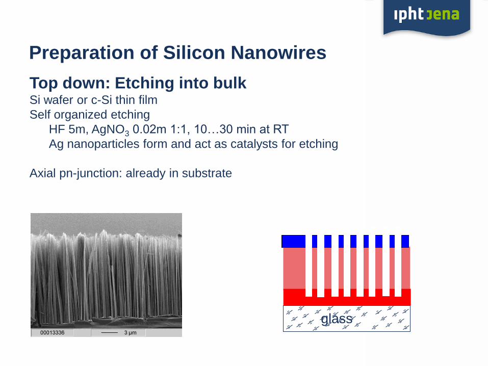
Preparation of Silicon Nanowires
Both preparation methods
• work on wafers
• work on Si thin films
• give single crystalline wires
Top down:
Etching into bulk Self organized etching
by HF + AgNO3
Bottom up:
Growth on substrate VLS growth (vapor liquid solid)
Wagner&Ellis 1964

Preparation of Silicon Nanowires
Bottom up: Growth on silicon substrate VLS growth
Au nanodots as template
Deposition of Au nanoclusters or
1 nm Au film heated to above eutectic temperature of 370°C
Thermal CVD from silane at 500°C: Au acts as catalyst for SiH4 decomposition
Doping by adding B2H6 or PH3
Axial pn-junction: Doping can be changed during growth
5 µm
Preparation of Silicon Nanowires
Top down: Etching into bulk Si wafer or c-Si thin film
Self organized etching
HF 5m, AgNO3 0.02m 1:1, 10…30 min at RT
Ag nanoparticles form and act as catalysts for etching
Axial pn-junction: already in substrate
p
n++
glass

Preparation of Nanowires on Si Films on Glass
Multicrystalline Si films produced by
laser crystallization of a-Si on glass
0.5 mm
EBSD map
of Si substrate layer:
100 µm grains
Etched nanowires different morphologies
on different grain orientations
VLS grown nanowires
3 µm

Preparation of Solar Cells
Substrate:
Si wafer or laser crystallized multicrystalline silicon film on glass
n-doped, acting as back contact
Etching of nanowires by HF + AgNO3
Carefully removing Ag nanoparticles
Depositing a-Si:H by PECVD to cover nanowires by shell
Layer sequence intrinsic 2 nm + p-doped 4 nm
Filling space between nanowires by TCO
ZnO:Al by ALD or sputtering
Front contact
Radial hetero-junction
Elektrode
SiO2
Glas
c-Si n++
n
n
Glas
a-Si
i/p+
n
TCO
c-Si n+
n

Preparation of Solar Cells
Radial hetero-junction
TEM Investigations
by N. Petkov,
Tyndall, Cork, Ireland
Si wafer Etched NWs
TCO 200 nm
400 nm
SiNW 1
2
30 nm
500 nm

Results: Optical Properties of Nanowire Carpets Improved absorption of visible light
Nanowires etched into Si thin films
Similar result for grown nanowires
Instrinsic light trapping
Optical properties measured in integrating sphere
1.5 µm thick layer

Results: Cells from VLS Grown Nanowires
On highly doped substrates:
Dopant deployment: No photovoltaic behavior of wires
n-doped nanowires on p-doped wafer
Voc 260 mV n-doped nanowires on
p-doped silicon thin film on glass
shunting!
Axial p-n-junction
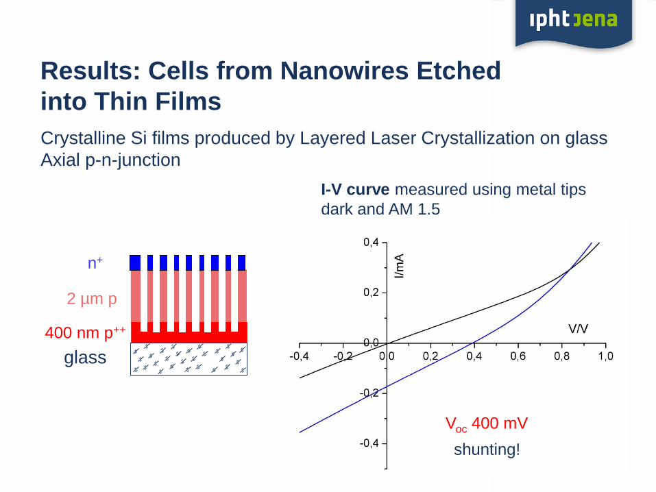
Results: Cells from Nanowires Etched
into Thin Films
Crystalline Si films produced by Layered Laser Crystallization on glass
Axial p-n-junction
I-V curve measured using metal tips
dark and AM 1.5
p
n++
glass
400 nm p++
2 µm p
n+
Voc 400 mV
shunting!

-1,0 -0,8 -0,6 -0,4 -0,2 0,0 0,2 0,4 0,6 0,8
-20
0
20
40
60
80
Cu
rre
nt d
en
sity (
mA
/cm
2)
Voltage (V)
AM 1.5
Dark7.29%
Voc
: 476 mV
Jsc
: 27.03 mA/cm2
FF: 0.562
Results: Cells from Nanowires Etched
into Wafer
Radial a-Si hetero-junction
7.3 % efficiency
Voc 476 mV
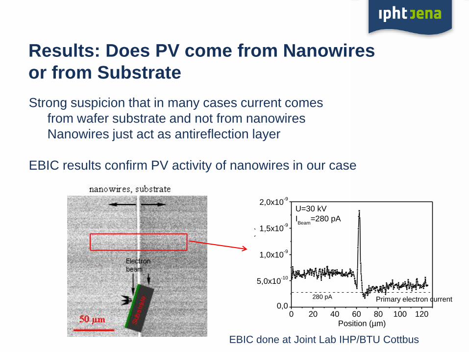
Results: Does PV come from Nanowires
or from Substrate
Strong suspicion that in many cases current comes
from wafer substrate and not from nanowires
Nanowires just act as antireflection layer
EBIC results confirm PV activity of nanowires in our case
0 20 40 60 80 100 1200,0
5,0x10⁻¹⁰
1,0x10⁻⁹
1,5x10⁻⁹
2,0x10⁻⁹
EB
IC c
urr
en
t (A
)
Position (µm)
U=30 kV
IBeam
=280 pA
280 pA Primary electron current
EBIC done at Joint Lab IHP/BTU Cottbus
-1,5 -1,0 -0,5 0,0 0,5 1,0 1,5 2,0 2,5 3,0 3,5-3,0x10
-3
-2,5x10⁻³
-2,0x10⁻³
-1,5x10⁻³
-1,0x10⁻³
-5,0x10⁻⁴
0,0
5,0x10⁻⁴
1,0x10⁻³
Cell 28+29
Cell 28+29+30
Cell 28+29+30+7
Cell 28+29+30+7+8
Cell 28+29+30+7+8+31
Cell 28+29+30+7+8+31+32
Cu
rre
nt (A
)
U (V)
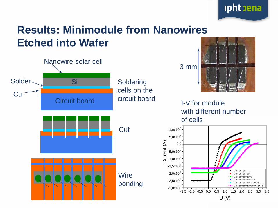
Results: Minimodule from Nanowires
Etched into Wafer
Nanowire solar cell
Si Solder
Circuit board Cu
Wire
bonding
Cut
Soldering
cells on the
circuit board I-V for module
with different number
of cells
3 mm
Open Questions
Optimal diameter and orientation of wires
Doping during VLS growth
Influence of Au in VLS grown wires
Reason for shunting and how to avoid it
Removing metal particles from holes between nanowires
Ag for etched nanowires
Surface passivation
Contacting cells
Summary
Silicon nanowire solar cells were prepared
• with axial or radial pn-junction
• on glass
• grown by VLS from Au templates on c-Si thin films: axial
• etched into wafers or into c-Si thin films with doping profile: axial
• radial a-Si heteroemitter
• perfect light trapping in nanowire carpet
• Voc 260 mV: VLS grown nanowire cell on wafer, axial p-n-junction
• Voc 476 mV, 7.3% efficiency:
Nanowires etched into wafer, radial a-Si heteroemitter, AZO contact
Acknowledgement
N. Petkov, Tyndall, Cork, Ireland
TEM investigations
M. Kittler, W. Seifert, Joint Lab IHP/BTU Cottbus, Germany
EBIC measurements
Funding
EC: SiNAPS Grant 257856 FP7-ICT-2009-5
EC : NanoPV Grant 246331 FP7-NMP-2009-SMALL-3


