Rochester Institute of Technology Rochester Institute of Technology RIT Scholar Works RIT Scholar Works Theses 2005 Silicon-on-insulator waveguide structures for electro-optic Silicon-on-insulator waveguide structures for electro-optic applications applications Christopher Harvey Follow this and additional works at: https://scholarworks.rit.edu/theses Recommended Citation Recommended Citation Harvey, Christopher, "Silicon-on-insulator waveguide structures for electro-optic applications" (2005). Thesis. Rochester Institute of Technology. Accessed from This Thesis is brought to you for free and open access by RIT Scholar Works. It has been accepted for inclusion in Theses by an authorized administrator of RIT Scholar Works. For more information, please contact [email protected].
Transcript
Rochester Institute of Technology Rochester Institute of Technology
RIT Scholar Works RIT Scholar Works
Theses
2005
Silicon-on-insulator waveguide structures for electro-optic Silicon-on-insulator waveguide structures for electro-optic
applications applications
Christopher Harvey
Follow this and additional works at: https://scholarworks.rit.edu/theses
Recommended Citation Recommended Citation Harvey, Christopher, "Silicon-on-insulator waveguide structures for electro-optic applications" (2005). Thesis. Rochester Institute of Technology. Accessed from
This Thesis is brought to you for free and open access by RIT Scholar Works. It has been accepted for inclusion in Theses by an authorized administrator of RIT Scholar Works. For more information, please contact [email protected].
Silicon-on-Insulator Waveguide Structures for Electro-optic Applications
By
Christopher T. Harvey
A Thesis Submitted in Partial fulfillment
of the Requirements for the Degree of
Master of Science In
Microelectronic Engineering Approved by: Professor ____________________ Dr. Karl D. Hirschman (Thesis Advisor) Professor ____________________ Dr. Santosh Kurinec (Department Head) Professor ____________________ Dr. Sean L. Rommel
Department of Microelectronic Engineering College of Engineering
Rochester Institute of Technology Rochester, New York
May 2005
ii
Acknowledgement
I would like to thank everyone that has helped me with this project during my
studies at the Rochester Institute of Technology. First my thesis advisor Professor Karl
D. Hirschman, always available for some one on one discussion about the SOI optical
modulator project. Professor Thomas Brown and Jason D. Neiser at the University of
Rochester for their research in the optics field and for making this project possible.
Special thanks go to Jason for helping develop process recipes, SEM imaging and device
testing. Without Jason this project would not have been possible. I also want to thank
my thesis committee members Dr. Sean Rommel and Dr. Santosh Kurinec for the support
and guidance through this process.
I would like to thank everyone in the Semiconductor and Microsystems
Fabrication Laboratory at RIT for their help and support (Al, Scott, Tom, Sean, Jeff
Peterson, Dave, Bruce, John and Rich). I want to thank the Hirschman Research Group
for providing a sounding board to bounce ideas off of (Rob S., Rob M., Jeremiah, Vim
and Jeff). I wish to thank my friends Sean Houlihan and Nate Wescott for their help
tackling some difficult problems that my process flow presented. Microelectronic
Engineering seniors have helped with some experimentation in the way of senior projects
and I want to thank Don Hamilton and Robin Joyce for their help in this project. Without
the work and knowledge gained from Charles F. Faisst I would not have been able to
finish, and I thank him for his help. The faculty and staff (especially Sara Widlund and
Charles Gruener) in the Microelectronic Engineering program have helped me with many
challenges in my coursework and project. Finally I want to thank my wife, Sandie.
iii
Silicon-on-Insulator Waveguide Structures for Electro-optic Applications
I, Christopher T. Harvey, herby grant permission to the Wallace Memorial Library, of the
Rochester Institute of Technology, to reproduce my thesis, in whole or in part, with the
knowledge that any reproduction will not be for commercial use or profit.
Student_____________________ Christopher T. Harvey
iv
ABSTRACT Silicon based photonic devices have been demonstrated by industrial leaders in
the microelectronic industry. The need for system integration has pushed the
development of silicon as a photonic material to new levels. This report presents details
on a silicon-on-insulator waveguide structure based on a metal Bragg reflection
diffraction grating, which utilizes a change in refractive index caused by a carrier change
to induce optical modulation. The motivation of the device was for use as an electrically
controlled optical modulator operating in the near infrared region; an optically controlled
device has been demonstrated in previous work. This study has thoroughly examined the
process development and electrical characteristics of the device through use of Silvaco™
simulation software and experimentation. The device has exhibited excellent optical
characteristics and has shown promise as an optical modulator and a sub-bandgap photon
detector. A silicon-on-insulator waveguide structure specified to operate at a wavelength
of 1053nm has been simulated, designed, fabricated and tested both optically and
electrically. Future iterations have been simulated and designed to take advantage of
advanced microelectronic processes.
v
TABLE OF CONTENTS Abstract iv List of Tables vi List of Figures vii Chapter 1: Introduction 1 Chapter 2: ORPEL Structures: Theory, Operation and Application 9 2.1 Mach-Zender Interferometer 9 2.2 ORPEL Structures 11 2.3 Modulation of ORPEL 12 2.4 Rigorous Coupled Wave Analysis 13 2.5 Mask Design 16 Chapter 3: Fabrication and Performance of ORPEL Waveguides 17 3.1 Thin Film Process Development 18 3.1.1 Starting Substrate 18 3.1.2 Local Oxidation of Silicon 18 3.1.3 Thin Film Processes 18 3.2 Electrode Definition 19 3.2.1 Resist Profile Engineering 19 3.2.2 Lithographic Critical Dimension 22 3.2.3 Focus Exposure Array 23 3.2.4 Metal Deposition and Liftoff 24 3.2.5 Liftoff Process 25 3.3 Scanning Electron Microscopy 26 3.4 Optical Reflectance Spectra 26 Chapter 4: Device Designs for Electro-optics and Optoelectronics 28 4.1 Silicon Lasing 29 4.2 Methods of Operation 30 4.2.1 Reverse Bias P-I-N Diode 31 4.2.2 Schottky Diode Based Sub-Bandgap Photodetector 34 Chapter 5: Conclusion 37 5.1 Summary of Work Performed 37 5.1.1 Device Design 37 5.1.2 Process Development and optical spectrum 37 5.1.3 Electrical Device Simulation 38 5.1.4 Sub-Bandgap Detectors 38 5.2 Future Work 38 References 40 Appendix I: Process Flow 42 Appendix II: L-Edit Mask Design Code 55
vi
LIST OF TABLES Table 1: Device parameters 11
vii
LIST OF FIGURES Figure 1: Silicon based optical modulator 2 Figure 2: Ideal reflectance graph 4 Figure 3: ORPEL schematic 5 Figure 4: Time resolved optical pulse device modulation 6 Figure 5: Mach-Zender Interferometer 9 Figure 6: Interference intensity vs. phase 10 Figure 7: Time resolved optical pulse device modulation 13 Figure 8: Theoretical transmittance, reflectance and absorption 14 Figure 9: Theoretical to experimental matching 15 Figure 10a: Previous-generation layout 16 Figure 10b: Current-generation layout 16 Figure 11: Device cross section 17 Figure 12: Resist profile with stringers present 20 Figure 13: Optimal resist profile 21 Figure 14: Device cross section 22 Figure 15: Metal lines with stringer influence 25 Figure 16: Final device reflectance spectra 27 Figure 17: Optical intensity within the silicon waveguide 28 Figure 18: Continuous wave Silicon Raman laser 30 Figure 19: Time resolved optical pulse device modulation 31 Figure 20: Uniform carrier generation 32 Figure 21: Open circuit hole concentration 32 Figure 22: Short circuit hole concentration 33 Figure 23: Reverse bias with and without illumination 33 Figure 24a: Reverse bias p-i-n with varying applied bias 34 Figure 24b: Reverse bias p-i-n diode speed comparison 34 Figure 25: Schottky diode IV characteristics 35 Figure 26: Detector spectrum 36 Figure 27: Front-side ground-plane contact 39
1
CHAPTER 1
Introduction
The semiconductor and microelectronics industry has a large working
infrastructure for use with silicon and silicon based products. Integrated circuits and
micro-electro-mechanical systems (MEMS) have become well-established industries
using silicon as a substrate. The latest trends involve “system on a chip” technology
where integrated circuits are combined with MEMS through clever changes in front-end
and back-end processing. The advantage of system on a chip is a drastic reduction in cost
by combining fabrication and packaging.
Optical systems have not yet been integrated with device driver/controller
technology, primarily due to material incompatibility. For optical modulators the
material of choice is lithium niobate (LiNbO3). Current phase modulators from New
Focus operate at frequencies from 100MHz to 9.2GHz with costs ranging $3,375 to
$5,570 [1]. These optical components are discrete, non-integrated modulators that rely
on external drivers and controllers.
Cost is the major factor driving silicon based optoelectronics research. The large
infrastructure for silicon processing combined with the widespread use of silicon in
microprocessors would allow for integration between various components at a much
lower expense. While packaging would remain a large portion of the cost of a device, it
would be possible to dramatically reduce manufacturing costs by utilizing the large
300mm substrates compared to the 100mm substrates available for LiNbO3; the 300mm
wafer has 9 times the area of the 100mm substrate. The devices can be seamlessly
integrated with controller and microprocessor technology, reducing packaging costs.
Silicon offers decreased packaging costs, improved interconnect performance and
decreased fabricating costs. The reasons why silicon is preferable are clear and one of
the major semiconductor manufacturers is leading the way.
Intel Corporation fabricated a silicon-based waveguide that functioned as a bridge
between traditional optical modulator technology and current MOSFET technology [2].
By combining a Mach-Zender waveguide with a polysilicon MOS capacitor it was
2
possible to induce a phase shift in the waveguide by operating the capacitor in an
accumulation mode.
Figure 1: This device is constructed using silicon-on-insulator. A MOS capacitor is fabricated by a 120Å gate oxide on the n-type doped 1.4µm single crystal silicon layer. The gate material is polysilicon, doped p-type 3 x 1016cm-3. The polysilicon is formed into a rib by depositing it within a 2.5µm contact opening created in oxide. The polysilicon rib represents the center of the waveguide. The rib is controlled on both sides by metal contacts.
The phase shift was induced over an 8mm distance. Operating in accumulation
mode, only a depth of 5nm of free carriers are manipulated within the waveguide. This
accumulation happens at the semiconductor/gate dielectric interface of the waveguide,
not in the center of the rib. Since the free carriers are added in a weak region of the
electric field there will be a small ∆n that must be propagated over a long distance to shift
the phase.
The Intel design has some drawbacks, which are addressed by the design
presented in this thesis. First, packaging becomes more difficult as the incoming
radiation must be coupled into the edge of the device, rather than using normal incidence
to the waveguide structure. Second, the size of the device consumes CMOS real estate,
reducing the integration advantage of using silicon. Other groups have demonstrated
silicon optical modulators using a p-i-n waveguide that have only modulated in the low
MHz range [3-6]. Both the MOS and p-i-n devices have exhibited frequencies that are
still below that of LiNO3. By switching to a voltage driven design, the current density
issue has been replaced by an electric field (capacitance) issue. The voltage is limited by
the maximum electric field that the gate dielectric can withstand. This maximum voltage
can be extended beyond the classical electrostatic model used in most textbooks if the
device operates in a deep depletion state [7].
3
There are three major factors limiting the use of silicon in optoelectronic
technology: First, due to the centrosymmetry of silicon, Pockel’s effect is not present.
Second, no linear electrooptic effect exists in silicon. Third, since silicon is an indirect
semiconductor, photonic emission is statistically improbable and practically impossible
[8].
Silicon does exhibit some optoelectronic effects and has been thoroughly studied
by Soref and Bennett [8]. The optical absorption spectrum of silicon can be modified by
an external electric field. This is known as the Franz-Keldysh effect [8] and when
referring to refractive index is known as electrorefraction. Another phenomenon caused
by a change in electric field is the Kerr effect, where a birefringent state is created
through the application of an electric field. The relationship between ∆n and ∆α has been
discussed in several textbooks and journal articles [8, 9]. Unfortunately the Franz-
Keldysh effect and the Kerr effect are weak in silicon with an expected ∆n of around 1 x
10-4 requiring an electric field approaching the dielectric breakdown strength of silicon
[8].
Another phenomenon that strongly modifies the refractive index of silicon is free
carrier effects. By changing the free carriers in a silicon sample, the refractive index can
be modified. Free carrier absorption, Burstein-Moss bandfilling and Coulombic
interactions between carriers and impurities [8] are all important effects that occur
simultaneously. Bandfilling and Coulombic effects affect the refractive index change in
an opposite manner in silicon. Bandfilling causes a shift to shorter wavelength and
Coulombic effects result in a shift to longer wavelength. The Coulombic effects are
strongest as a spectrum shift to longer wavelengths is observed [10]. The change in free
carriers can come from an injection of carriers into an undoped sample (∆N) or it can
come from removal of carriers from a doped sample (-∆N). When absorption is
negligible it makes little difference optically whether the free carriers are added or
removed. Changes in effective index of refraction are around 1 x 10⁻² for a change in free
carriers of 1 x 1019cm-3 for an incident wavelength of 1550nm [9].
In order to realize a monolithic photonic device in silicon technology, a design
must be drafted to exploit the optoelectronic effects that are present in silicon. The key
constituent of the device is the optically resonant periodic electrode (ORPEL)
4
arrangement. The ORPEL based device is highly sensitive to changes in the effective
index of refraction, as well as the structural parameters.
Figure 2: In this figure an ideal resonant situation is applied. The y-axis represents normalized reflectivity and the x-axis is the incident light wavelength. The reflectivity is very high in all regions except at a wavelength equal to 1.55µm. This is the resonant wavelength for the modulator structure where the device is tuned to have a very abrupt drop in specular reflection. This figure demonstrates that a small shift in resonance would create a large shift in specular reflection.
An ORPEL structure is a diffraction grating embedded into a waveguide. Normal
incidence radiation is coupled into the waveguide, while the diffraction gratings also
work to confine the radiation via Bragg reflection. Finally, the ORPEL structures
provide the necessary stimulus to electrically perturb the effective refractive index of the
waveguide. Unperturbed structures have a high specular reflectivity with a well defined
low in the reflectance spectra at the resonance wavelength. By changing the effective
index of refraction of the waveguide, the resulting resonance wavelength shift can enable
optical switching.
5
Figure 3: The device dimensions of importance are the pitch and material thicknesses. These dimensions provide the necessary resonance for the device to operate at the proper wavelength.
All parameters except for the effective refractive index, neff, are constant for a
given structure. The structure is very sensitive to small changes in any changes to the
parameters of the structure. By changing neff, the resonant wavelength of an ORPEL
structure can experience a spectral shift. Figure 4 demonstrates switching in an optically
modulated mode of operation [11]. As the intensity of the source increased, more carriers
are being generated due to absorption. At a certain point the carrier generation was
sufficient for the resonant wavelength to shift, resulting in an intensity induced change
(decrease) in the reflected intensity.
W
L
Electrode Bus
Grating finger
(electrode)
SiO2 Overcoat
Not to Scale
Pitch
SOI
6
Figure 4: Time resolved graph that shows a rise in intensity of the reflected pulse as the input pulse intensity increases. When the input intensity is high enough a decrease in reflected intensity is observed. This is due to an increase in free carriers causing a resonant shift in the ORPEL structure to specular intensity minima [11].
Three device generations have been designed and fabricated. Each device builds
on experience from the previous model. The first-generation device relied upon a
Schottky diode to provide carrier injection. The second-generation device used Schottky
injection, but also grounded one set of electrodes through an ohmic contact to eliminate
back-to-back diode leakage. The current third generation device is using a different
strategy. A gate dielectric is used to steer carriers that have been optically generated.
The first-generation device was set up to modulate the telecommunication
wavelength of 1550nm. The test structure was designed to allow for variations in film
thickness by including a range of pitches in the waveguide. The device was fabricated at
the Rochester Institute of Technology by Charles F. Faisst [12] and tested by Jason D.
Neiser at the University of Rochester. Testing was accomplished by scanning an incident
light beam’s wavelength from 1510 –1590nm and measuring the light intensity that was
reflected from the structure. A well-defined drop in reflectance at 1550nm was observed
with the 0.78µm pitch device, providing a good correlation between theoretical and
experimental data.
The second-generation device utilized the same mask set as the first generation.
The major fabrication differences were the switch from a titanium/aluminum stack to
using only aluminum. This allowed for better Schottky contacts to be formed. The
7
second change was a masked implant that created ohmic contacts for every other
electrode by implanting high doses of phosphorus. One advantage of this device was for
IR detection, made possible through the improved contact arrangement.
The third-generation device uses the same principles for optical operation as
device gen. one and two, but applies them to a different wavelength. New electrical
schemes for modulating the device were developed and a preliminary ‘passive’ device
was fabricated to verify optical operation and gather high-speed electrical performance
data. This latest device offers new opportunities since it employs a wavelength absorbed
by silicon.
SOI waveguides operating as an optical modulator have been designed, simulated,
fabricated and tested. An evolutionary process has led to the most recent device design
and test chip layout. Various designs were examined before deciding on final device
specifications. Optical and electrical modeling combined with experimental data from
previous generations was used to determine the final design for use in the third
generation.
This thesis will be presented ideologically rather than chronologically to improve
cohesiveness of ideas. Chapter two will be devoted to the theory and application of the
ORPEL structure, including a comparison between ORPEL and Intel’s device. The Intel
modulator is based on a Mach-Zender interferometer and uses free carrier effects in
silicon to modify the index of refraction. The ORPEL device uses a Bragg diffraction
grating to couple light into a waveguide region and is sensitive to changes in the index of
refraction; free carrier effects are also used in the ORPEL device.
Chapter three will discuss process development and integration for the ORPEL
device. A process flow that is not device specific is presented. Development of the thin
film processes and metal electrode definition process are explained in greater detail than
the general process flow outlined at the beginning of this chapter. Finally, passive optical
spectra is presented and evaluated.
Chapter four will explain the active, or electrically modulated, device design,
theory and operation. The active device design and theory is described along with the
details of device simulation. The impact observed using different modulation schemes
8
was factored into the final design used in testing the active and passive devices.
Simulation results are presented which can be used in future devices.
Chapter five will be a summary and conclusion of the work presented in this
thesis. Future designs are considered that could be implemented as the technology
advances.
9
CHAPTER 2
ORPEL Structures: Theory, Operation and Application
The theory and application behind the Mach-Zender Interferometer (MZI) will be
examined. The MZI-based optical modulator designed and fabricated by Intel Corp. will
be compared in detail to the device presented in this thesis. The ORPEL device design
procedure will be investigated by describing iterative modeling process used to determine
the specific device parameters needed to achieve desired optical characteristics.
2.1. Mach-Zender Interferometer
An interferometer works by splitting an optical wave into two waves using a
beamsplitter. The two waves travel different optical path lengths, are directed using
mirrors and finally recombined using a beamsplitter. The final superpositioned waves
intensity can then be detected.
Figure 5: Mach-Zender interferometer showing equal length legs with electrical contacts around one of the legs. An applied bias will change the refractive index of the material (through the Pockel’s effect in the case of LiNbO3) and allow for total destructive interference. Image taken from Photonics [9].
The intensity of the superpositioned wave is can be represented by the following
equation [9]:
+=
λπ dII o 2cos12 (1)
10
The path-length difference changes the phase of the two beams. When they are
superimposed, there is either constructive or destructive interference that will determine
the exit intensity. Fully destructive interference will result in a final intensity of zero.
This occurs when the path difference is equal to λ/2. When d = λ/2 the normalized
intensity is zero as seen in the following graph.
Interference Intensity
0
0.1
0.2
0.3
0.4
0.5
0.6
0.7
0.8
0.9
1
0 0.1 0.2 0.3 0.4 0.5 0.6 0.7 0.8 0.9 1
d/λ
Nor
mal
ized
Inte
nsity
Figure 6: When d/λ is equal to 0.5 the normalized intensity of the beam is zero, due to completely destructive interference.
A Mach-Zender interferometer operates by splitting a beam into two legs and
inducing a π phase shift in one of the legs. When the two beams are brought back
together the phase shift will create destructive interference and give an effective output
intensity of zero. This design is currently used in LiNbO3 optical modulators as this
material exhibits Pockel’s effect allowing electrical manipulation of optical properties.
Silicon does not exhibit Pockel’s effect, so a less direct method needs to be used if a MZI
design is desired.
The device reported by Intel is a MZI-based design that uses electrorefraction of
silicon to induce a phase shift [2]. The device uses a MOS structure in accumulation
mode in order to increase the electron concentration significantly at the semiconductor
surface. The phase shift is prompted by altering the carrier concentration in one leg of
the structure; modifying the effective index of refraction, neff. The change in refractive
index is predicted by equation 2.2 [8].
11
∆+
∆×
−=∆ **22
22
8 ch
h
ce
e
o mN
mN
ncen
επλ
(2)
By inducing a ∆neff it is possible to change the speed of the traveling wave relative to the
other leg of the MZI. Given a specific ∆neff it is necessary for the length of the leg to be
long enough to allow for a superpositioned wave intensity to be zero; Intel reported a
length of 8mm for their MZI design [2].
2.2. ORPEL Structures
ORPEL structures are essentially a guided-mode resonant filter operating in a
linear waveguide. A narrow wavelength band is allowed to couple into the waveguide
based on waveguide device parameters. Electrorefraction is the effect used to alter the
refractive index of the waveguide region. By changing the number of free carriers it is
possible to change the refractive index. Either an increase or a decrease in free carriers,
through injection or by redistribution of carriers can be used. More importantly the
effects can be localized to the most intense portion of the electric field through tuning of
the ORPEL design. The parameters presented in table 1 have a very small tolerance that
must be met for the on-resonance reflectance spectrum to match figure 3.
Table 1: The design parameters for the ORPEL structures.
Design parameters – 1550 nm device Substrate type p-type Buried oxide thickness 3.006 µm Silicon on insulator thickness – manufacturer 1.5 µm Silicon on insulator thickness – final 1.26 µm Aluminum thickness 0.05 µm Oxide overcoat thickness 0.39 µm
12
2.3. Modulation of ORPEL
The motivation behind the SOI waveguide structure was for an optical modulator
designed to work in the near-infrared region. The modulation of the device is achieved
by altering one of the parameters in table 1, which will change the resonant wavelength
of the device. A change in resonant wavelength changes the reflectivity of the device,
allowing for a reflectance low when on-resonance to a reflectance high when off-
resonance.
The incident wave is coupled into the waveguide via the diffraction grating; a first
order approximation of this waveguide coupling is presented in equation 3 [11].
Λ+=⋅
πθλπ
λπ 2sin22 mneff (3)
Where λ is the wavelength of the incident light, Λ is the grating period, θ is the incident
angle, neff is the effective index of refraction, and m is an integer corresponding to the
mode number.
The wave must be confined to the waveguide to operate at a low loss level. In
addition to waveguide coupling the metal electrodes provide Bragg reflection,
establishing a standing wave within the waveguide. The Bragg detuning is determined in
equation 4 [13]; when δ goes to zero, the Bragg condition is satisfied.
Λ
−=12
λπδ effn
(4)
Where λ is the wavelength of the incident light, Λ is the grating period, and neff is the
effective index of refraction.
For the on-resonance situation, both the waveguide coupling and the Bragg
reflection equations must be satisfied. The resonant wavelength, λ, will change if any of
the parameters in equations 3 and 4 are modified either through physical changes in the
structure, a change in incident wavelength, a change in incident angle or a change in
refractive index.
In silicon, free carrier effects will change the refractive index. This follows the
parameters set forth in equation 2. The change in refractive index is based on the
magnitude of the free carrier change; the change in reflectance spectra is dependent on
the sensitivity of the device. A small change in refractive index will create a large
13
change in reflectivity with a device designed to have a narrow resonance. This has been
demonstrated through optical generation of carriers. As the intensity of the input laser
increased, the number of free carriers increased up to the point where the refractive index
change allowed for a shift in resonant wavelength. This situation has driven the research
to move from optical carrier manipulation to electronic carrier manipulation.
Figure 7: This is a time resolved graph that shows a rise in intensity of the reflected pulse as the input pulse intensity increases. When the input intensity is high enough a decrease in reflected intensity is observed. This is due to an increase in free carriers causing a resonant shift in the ORPEL structure to specular intensity minima [11].
2.4. Rigorous Coupled Wave Analysis
Rigorous coupled wave analysis or RCWA is used to determine the physical
device parameters that will yield the most defined on-resonance state. The goal is to have
the largest difference in reflectivity between on-resonance and off-resonance. RCWA
calculates the reflectance, transmittance and absorption of the waveguide based on the
material optic properties, material thickness and electrode spacing (pitch). Small changes
in materials used, thickness and pitch can be utilized to provide an optimized design for
fabrication.
Modeling of the ORPEL device is accomplished by solving Maxwell’s equations
using a differential form. The method used is rigorous coupled wave analysis (RCWA).
The permittivity of the grating layer is represented as a Fourier series. A solution to the
eigenvalue problem derived from Maxwell’s equations is found for the grating structure.
Boundary conditions are then applied to the input and output filters of the structure to
14
determined diffraction efficiencies (for reflection, transmission and absorption) [14].
These are then plotted (against designed pitch or wavelength) to determine the device
resonance. Where the diffraction efficiency for reflectance is at a minimum establishes
the resonant wavelength of the device. The goal of the design iterations (testing different
parameters) is to provide the deepest and narrowest reflectance spectra possible at the
desired resonance wavelength.
Figure 8: TE reflection, transmission and absorption spectra for a 0.9 micron grating period design.
The RCWA method is exact and does not rely upon approximations. This allows
for excellent theoretical and experimental matching (see figure 9). The software
developed by the Institute of Optics at the University of Rochester [15,16] requires an
iterative process to determine optimal device specifications. The variables available for
modeling are material thicknesses, diffraction grating pitch, and refractive indices of
materials. Small variations in these parameters are applied systematically to determine
what variables have the most impact over resonant wavelength.
15
Figure 9: Excellent experimental to theoretical matching is observed in this figure. The reflectance of the device follows the RCWA generated plot.
Pattern definition of the grating electrodes has the most direct influence on the
resulting spectral response. The following section describes the electrode layout that was
used in device fabrication.
16
2.5. Mask Design
Due to the requirements on critical dimension control and defects, the ORPEL
electrode reticles were manufactured by outside photomask vendors (Photronics, Inc. &
Dupont Photomask). Both masks utilized various pitch arrangements to allow the device
to be used for different wavelengths, and/or to account for any process variation that
could affect the final resonance. The most recent mask design utilized script files for
layout to ensure exact dimensions were maintained for the various grating periods
ranging from 0.68µm to 1.08µm. The ORPEL structures were configured large enough
to avoid losses (light escape) and ensure there was adequate interaction distance within
the waveguide. They were arranged as both rectangles (1mm x 150µm) and circles
(500µm diameter) to explore geometric differences. An example script file for the
circular devices can be found in appendix B.
(a) (b)
Figure 10: a) The first electrode mask. b) The most recent mask design, which utilizes a higher device density to allow for more optical experiments. The mask was designed using scripts written in Ample and C-programming.
17
CHAPTER 3
Fabrication and Optical Performance of ORPEL Waveguides The SOI electro-optic project utilized unit processes that are standard to the
Semiconductor and Microsystem Fabrication Laboratory (SMFL). These processes will
not be covered in this thesis, as they are part of the common knowledge base in
microelectronics. The general fabrication sequence is presented in this section.
Figure 11: Cross-section of the finished device. The dimensions laterally and vertically of the device are critical to proper operation.
The crystalline silicon layer of the SOI substrate must be thinned to the correct
thickness based on the wavelength used. This is done by oxide growth and etchback until
the desired thickness is met, providing superior control over the layer thickness. Growth
is performed using a dry oxygen ambient and etch is completed using a hydrofluoric
buffered oxide etch (BOE). A thin oxide is grown to provide electrical isolation for the
device. This region could either be left to remain or etched away from the active area
dependent on the mode of operation. Oxide removed would be applied for a bipolar
device or diode (i.e. Schottky, p-i-n) and oxide remaining would be used for field effect
modulation. Outside of the active region, local oxidation of silicon (LOCOS) isolates the
power supply lines from the substrate.
Metal is deposited via evaporation over a previously patterned photoresist to
define the ORPEL structures. Evaporation is preferred over sputtering to improve liftoff
yield and uniformity by providing a non-conformal (line-of-sight) deposition. Using a
solvent to dissolve the patterned photoresist, which removes the metal from unwanted
18
regions, completes the pattern transfer. Overcoat material (typically an oxide or silicon
thin film) is sputtered onto the wafer to complete the waveguide region. The material
used is dependant on the wavelength of operation. Silicon and silicon dioxide have been
used for the 1550nm and 1053nm devices, respectively. Other materials could be
sputtered depending on the optical properties and desired device operation.
A final contact cut through the overcoat layer completes the device. The thin
metal can be contacted directly or an optional secondary layer of metal can be deposited
to allow for probing and wire bonding. This section will discuss the unit process
development and integration of the most current device iteration, ORPEL 1053nm.
3.1. Thin Film Process Development
3.1.1. Starting Substrate
The initial substrate as received from vendor SOITECH had a crystalline silicon
(c-Si) thickness of 1.5µm and the design specifications require a silicon thickness of
0.7495µm. In order to meet the design specifications it was necessary to subject the
wafers to a series of dry oxidation and oxide removal steps. Oxide growth was measured
using monitor wafers and the average thickness grown was then used to determine the c-
Si thickness consumed by using the ratio of 46% silicon consumed for a given oxide
thickness grown. The accuracy of this method was verified using variable angle
spectroscopic ellipsometry at the University of Rochester by measuring the c-Si thickness
at two times during the thinning process.
3.1.2. Local Oxidation of Silicon (LOCOS)
LOCOS isolation was used to isolate the power supply lines from the c-Si.
Silicon nitride was deposited and patterned to protect the active region of the device. A
steam ambient oxidation was performed to grow 2500Å of oxide.
3.1.3. Thin Film Processes
The overcoat layer for the waveguide region was chosen to be SiO2. SiO2 is a
good choice since it is compatible with silicon, easy to pattern and exhibits a higher
refractive index than air, allowing for total internal reflection. SiO2 had to be deposited
19
onto the wafer surface instead of grown in order to allow for a conformal coat of the
electrodes. Initially three methods of SiO2 deposition were investigated: LPCVD oxide,
PECVD oxide and sputtering. Each method presented unique challenges.
LPCVD oxide or low temperature oxide (LTO) is performed using a hot-wall
vacuum system that introduces SiH4 and O2 to the system. At the temperature of 425°C,
the SiH4 and O2 breakdown and form SiO2 on the wafer surface. The main problem with
both CVD systems was the choice of metal for the electrode definition. By choosing gold
as the electrode metal, the wafers must be quarantined from any front-end CMOS tools
after gold is deposited. Both CVD systems are used in MOS manufacturing and therefore
can never have gold placed in the system.
An RF sputter system was located that was not used for MOS manufacture and
would be safe to process post-gold deposition. The system was run in an RF mode with a
forward power of 500W using a quartz target. The deposition rate was 10Å/min
requiring 390 minutes to complete the overcoat layer. The within wafer uniformity was
improved by breaking vacuum halfway through the sputter and rotation the wafer 180
degrees. The optical properties of the film were verified through variable-angle
spectroscopic ellipsometry (VASE).
3.2. Electrode Definition
3.2.1. Resist Profile Engineering
The capabilities of i-line lithography presented unique challenges to electrode
imaging. The electrode dimensions were between 0.34µm and 0.5µm and the i-line tool
had a specified CD of 0.5µm. In order for these images to be resolved multiple process
steps needed to be examined including the resist sidewall profile and critical dimension.
Due to these challenges, lithography was the factor that required the majority of process
engineering time.
The patterning of metal lines and spaces is most commonly performed using
either a wet etch process or a chlorine based RIE. The metal used in this process, gold,
requires a cyanide-based wet etch. With proper precautions this etch can be safely
performed and is commonly used in III-V fabrication. Unfortunately the line sizes were
too small to use a wet etch due to the isotropic nature of the etchant. Gold also presented
20
challenges to use in a dry etch since the SMFL is primarily a CMOS laboratory; etching
gold in any front-end tool would be disastrous for CMOS processing. The only way to
pattern gold at the SMFL was through a lift-off process.
The entire lithography system was examined thoroughly to identify and separate
problem areas to optimize the process. Device dimensions (periods) on the new reticle
were very similar to those found on the older design. A screening experiment using
process parameters from previous device designs was implemented to determine how far
from the baseline the new mask would be. Negative resist, Clariant (AZ) nLOF 2010,
was coated onto a sample wafer at 3750RPM for a thickness of ~6500Å. An exposure of
78mJ/cm2 and a develop time of 45 seconds was used to pattern the resist. The lines and
spaces of these devices are on the order of 0.4 – 0.5µm, which is at the very limit of what
can be seen using optical microscopy. Under an optical microscope the samples appeared
well within tolerance.
Resist scum or scumming (figure 12) is the incomplete removal of resist from
areas that should be resist free. In the case of the optical waveguide, it was hypothesized
that resist was still in the spaces where metal should be contacting the substrate. This
would prevent proper adhesion and cause the metal lines to be removed from the device.
Figure 12: In the picture it can be seen that there is a significant stringer left on the resist base. This stringer translates directly to the deposited metal..
21
Since the resist profile was not conducive to liftoff after only increasing the
develop time another option was examined. By dry etching the resist in a short timed
reactive ion etch (RIE) it was possible to remove the scum at the bottom of the open
space, leaving a bare substrate for metal to deposit and adhere. The develop time of 60
seconds was used as the resist lines and spaces were well controlled and the amount of
scum necessary to remove less than that the amount of scum found in the 45 second
develop time.
An oxygen RIE was used to develop the descum recipe. Various etch times were
examined and finally an etch time of 30 seconds was chosen as it had the best resist
profile. It was necessary to examine these samples under a SEM to inspect for the
stringers seen in figure 12 above. Since the stringers would adversely impact the optical
characteristics of the device it was beneficial that the RIE removed the stringer leaving a
bare substrate and straight sidewalls.
The descum recipe called for 200W 50sccm O2 and 50mT. Etch depth is a
function of etch time so after a preliminary screening experiment using a 30 second etch
time, 15 seconds, 45 seconds and 60 seconds were used and the resulting resist profile
was inspected using scanning electron microscrocopy. The 30 second etch time had the
most uniform resist profile and was chosen as the descum process (figure 13).
Figure 13: Nearly optimal resist edge profile for a lift-off process. These resist fingers were manufactured using a 60sec develop time and a 30sec O2 RIE at 200W forward power. Note the resist footer is completely removed.
22
By analyzing the resist profiles it was possible to determine the major problem
that was plaguing liftoff: scumming. The solutions to this problem were twofold. First,
the develop time was increased to remove the majority of unexposed resist in the clear
areas between resist lines. Second a reactive ion etch descum process was developed to
remove any stringers left over from the develop process.
After the resist profile had been deemed satisfactory aluminum and gold was
deposited using evaporation. By removing the stringers the final metal lines were planar
as seen in figure 14.
Figure 14: The final device cross-sectioned showing the final gold electrodes which are perfectly flat and do not exhibit any sort of resist footer induced metal deformation.
3.2.2. Lithographic Critical Dimension
At the same time that liftoff was being examined the resolution in the resist within
chip was under close scrutiny. The resist thickness of 6500Å seemed to be too thick
since the depth of focus on the canon is only 5000Å. A large portion of devices were not
imaging properly, or were being overexposed resulting in no metal lines after liftoff. The
easiest solution was to make the resist thinner. The first attempt to reduce the film
thickness was to spin the wafer at a higher speed. The current process uses a speed of
23
3750RPM. Using a high-speed hand spinner at 5500RPM it was possible to get the film
thickness down.
Use of the high-speed spinner improved resolution but had an undesirable effect
of redepositing solvent on the film surface. Affected areas no longer had a uniform film
thickness. Instead there was a high degree of irregular circular anomalies on the wafer
surface. These translated directly to exposure and develop, resulting in poor yield. It was
found that the thinner resist had a higher resistance to scumming, although a stringer was
still present on the resist lines. This necessitated the descum process to be performed.
The second attempt utilized a solvent to reduce the viscosity of the resist.
PGMEA was added to the nLOF 2010 in a 1:1 ratio. 30ml of PGMEA and 30ml of
nLOF 2010. This changed the viscosity enough to allow a thickness of 1750Å at the
standard coat track maximum speed of 3750RPM. This allows a greater latitude in film
thickness since the film is already thinner than what is possible on the specialized hand
spinner at 5500RPM, and the spin speed can be decreased to get a thicker resist.
Inspection determined that the 1750Å resist developed good line space pairs in the
proper duty cycle with sufficient resist remaining after descum to allow successful liftoff.
Before the described changes were implemented, liftoff results were inconsistent; based
almost solely on chance. By analyzing the resist profiles it was possible to attack the
problem using science. This has created a repeatable, reliable and in control process for
liftoff and has removed one of the greatest hurdles that faced the fabrication of the
device.
3.2.3. Focus/Exposure Array
The focus exposure check (FEC) was used to determine the optimal focus
distance and exposure dose for the devices. The pitch is a fixed value set by the mask.
Altering the dose can vary the duty cycle of the pitch. By applying a focus exposure
matrix and examining the resist profiles using a scanning electron microscope (SEM) it is
easy to determine the optimal focus and exposure.
The focus is varied by rows starting at -0.5µm and increasing by 0.1µm. This
gives a fairly good range (1µm) for the focus to pass through. The sharpest image was
found at a focus offset distance of -0.2µm. This focus was best throughout all exposure
24
doses used and was set to the standard focus setting when shooting electrode lithography.
Dose was started at 75mJ/cm2 and increased by 1mJ/cm2. The best dose was found to be
80mJ/cm2.
3.2.4. Metal Deposition and Liftoff
Metal was deposited using evaporation and lifted off using Clariant AZ300T
heated to 85°C followed by an ultrasonic bath. The fingers had all lifted off and were no
longer in the device region or even on the wafer. The experiment was repeated with the
same results. The metal lines were removed after liftoff but large area metal remained.
These results indicated that the problem was resist scum.
The metal deposition needed to provide the same result every time, so the source
to wafer distance of 12.75” was held constant for every process run. An in-situ
deposition monitor was used to measure the metal thickness as seen on the wafer. This
monitor was calibrated by measuring the actual metal thickness using a profilometer.
This in turn was used to create a film specific tooling factor for the Inficon in-situ
thickness monitor.
A pre-evaporation was performed on a shutter to remove surface impurities from
the metal source. The evaporation shutter blocked the thickness monitor requiring the
chamber pressure gauge to be used to determine when evaporation was being performed.
After the metal evaporated on the shutter for 15 seconds, as indicated by the pressure
gauge, the shutter was opened. When the thickness was 1 second away from the target
(as determined by the material thickness and material deposition rate) the shutter would
be closed. This process was found to be very repeatable.
The wafer was always placed perpendicular to the metal source. This was to
improve the line of sight deposition characteristic of evaporation. By keeping the wafer
normal to the evaporated metal sphere it is more likely for the metal to deposit only on
the horizontal portions of the wafer and not deposit on the vertical sidewalls. The more
vertical the sidewalls, the better the metal deposition (less conformal). A best-case
scenario would be a sidewall that was beyond 90 degrees.
25
Figure 15: Note the metal ‘wings’ on this device. A resist stringer preventing an intimate contact between the silicon and metal caused this. The liftoff of these lines was compromised since only a small portion of the metal made contact with the substrate surface.
Metal thickness plays a crucial role in the operation of the waveguide region. The
original specifications called for a 100Å aluminum adhesion layer, with a 400Å gold
layer on top. For optical reasons it was desirable to have the aluminum adhesion layer as
thin as possible while still providing adequate adhesion, defined by the ability of the
fingers to remain on the substrate. It was found that a 30-50Å aluminum layer was still
able to provide adhesion for the gold, while removing the percent aluminum from the
metal stack.
3.2.5. Liftoff Process
The final problem associated with liftoff is redeposition of lifted off materials.
Suspended metal can redeposit on the wafer, creating killer defects. When the wafer is
removed from the solvent bath, metals suspended in the bath stick to the wafer instead of
washing away with the solvent. Since the solvent cools when the bath is placed in the
ultrasonic tank the best solution for eliminating redeposition is to a) never allow the
wafer to dry while particulates are still on the surface and b) use high pressure water to
remove any remaining solvent or particulate matter. This produces a clean wafer surface
devoid of lifted off material.
26
3.3. Scanning Electron Microscopy
The scanning electron microscope (SEM) was a vital tool in the development and
analysis of the SOI modulator application. The primary application for the SEM was to
examine the resist features throughout the electrode lithography process. Resist features
were examined before and after descum, varying develop times, varying descum times
and finally after liftoff. The information from the SEM proved invaluable in the
development process.
Additionally the SEM provided final measurements of device parameters that
could not be accurately measured during fabrication. Such parameters include final
device metal line width, LOCOS thickness, overcoat thickness and metal thickness.
Reasons for the inability to measure some features during fabrication are related to the
specific process used. For example, the metal thickness could not be measured because
the LOCOS thickness removed any known zero point, and the overcoat biased the
measurement due to close proximity of metal lines to each other. The SEM allows for
improvements to be made in future process iterations.
The photolithography experimental responses were line width and the presence of
resist scumming. Line width was measured using measurement annotation bars available
on the SEM. These were verified correct by examining the pitch of the line/space pair
(not influenced by process shifts). Small changes in the dose applied to the resist resulted
in appreciable differences in the resist line width and ultimately electrode duty cycle.
3.4. Optical Reflectance Spectra
Final optical reflectance spectra have been obtained through testing by the Institute
of Optics as the University of Rochester. The optical performance of the device can be
evaluated and the electrical modulation can be extrapolated by examining the narrowness
of the on resonance response. The results in figure 16 demonstrate that the tight
tolerances set forth by the RCWA software has been achieved.
27
Figure 16: Final reflectance spectra of the 1053nm device. The results demonstrate excellent on/off resonant behavior and narrow FWHM. This proves that the tight tolerances of the RCWA software have been achieved and that the device design is would require only small changes in refractive index to induce modulation.
The third resonance from the left demonstrates a very desirable spectrum. The difference
in reflectance between on resonance (specular reflection minimum) and off resonance
(specular reflection maximum) is 5dB and the FWHM of the device is ~1nm. This
response shows that switching between on resonance and off resonance by electrically
stimulating the carrier concentration is optically feasible. Electro-optic modulation is
discussed further in Chapter 4.
28
CHAPTER 4
Device Designs for Electro-optics and Optoelectronics Active devices operate by applying an external electrical signal to the electrodes.
This signal perturbs the free carriers enough to cause a distinct change in refractive index.
Different methods were investigated for electrical modulation of the ORPEL device. The
Schottky diode, MOS capacitor and p-i-n diode were all evaluated for use in the device
where each modulation method required a specific device design. Use of silicon is a
constant for all device designs limiting the current density and electric field to which the
waveguide could be subjected.
The main advantage for Schottky diodes is speed; Schottky devices have been
demonstrated at speeds in excess of 70GHz [17]. Although high-level injection using
Schottky contacts is possible, the carrier concentration is increased only near the
electrodes at the silicon surface. This reduces the effectiveness of the modulation scheme
by only perturbing carriers at the fringe of the optical field. In the ORPEL design, the
carrier concentration must be increased several orders of magnitude in the waveguide
region where there will be the most interaction with the optical energy. While there is
optical energy near the electrodes, in most designs the peak intensity was central to the
silicon layer as shown in figure 17.
Figure 17: Optical field intensity within the ORPEL waveguide. The darkest regions are the most intense where changes in refractive index will have the largest effect on the device operation.
29
Another method that has been utilized by industry leaders was the MOS capacitor.
The MOS capacitor in accumulation mode can increase the carrier concentration into the
range of 1e20cm-3. This carrier concentration change is limited to the silicon surface
within the first 3-5nm; this is outside of the highest intensity of the optical field for the
device (see figure 17). Using the capacitor in a deep depletion mode where the carriers
are removed will occur further into the silicon substrate, however, the carrier
concentration that can be depleted is limited to the breakdown strength of the insulator
and silicon. Depleting a 1e20cm-3 doped region in the central portion of the waveguide
would be virtually impossible, not ignoring the fact that it would be extremely difficult to
fabricate.
A forward bias p-i-n diode configuration has been utilized in silicon optical
modulators [3-6]. This method operates around the 20MHz range, and the change in
carriers is limited to 3e17cm-3 due to excessive current density [3-6]. Although the
forward bias strategy does not appear as suitable for high-speed and low-power
applications, the p-i-n diode does offer a modulation solution to the ORPEL structure.
An alternative to injection or accumulation/depletion modulation schemes is
utilizing optically generated carriers to provide the modulation stimulus, as demonstrated
by Sankey et. al. [11,18-20]. While carrier generation provides the necessary change in
refractive index, a method for carrier removal that is faster than thermal recombination is
required. Optical pumping is also used in a silicon laser built by Intel, and the same
concerns over carrier removal are present. The solution for fast carrier removal is to
utilize a reverse bias p-i-n diode.
4.1. Silicon Lasing
Intel Corporation has demonstrated a continuous wave silicon Raman laser [21]
that operates by optically pumping a waveguide structure with a 1550nm laser. The laser
output is then 1686nm. One of the biggest barriers that needed to be overcome was the
nonlinear optical loss caused by two-photon absorption (TPA) induced free carrier
absorption. TPA was reduced through the use of a p-i-n diode which would sweep excess
carriers out of the waveguide region, allowing a Raman gain to occur.
30
Figure 18: Intel continuous-wave Raman silicon laser. The p-region and n-region along with the center silicon rib make up the p-i-n diode. By applying a reverse bias to this diode it is possible to eliminate the free carrier absorption problem caused through two-photon absorption through removal of excess carriers.
This principle has been applied to the ORPEL waveguide structure in a way to
quickly sweep carriers out of the system allowing for a change in refractive index.
Optical modulation of the device has been demonstrated and shows that it is possible to
create enough carriers to shift the resonance of the waveguide. By including an electrical
control a higher degree of speed and freedom can be provided to the system.
4.2. Methods of Operation
Photogeneration of carriers occurs when light that possesses a photon energy (hν)
greater than the semiconductor bandgap is absorbed, creating an electron-hole pair. For
ORPEL modulation, the photogenerated carriers must increase to a high-level which can
change the refractive index and normal-incidence reflectivity. Self-modulation of the
ORPEL device has been demonstrated through the introduction of photogenerated
carriers, as shown in figure 19.
31
Figure 19: Time resolved input pulse and reflection response. When the input intensity is high enough, the structure establishes resonance and a decrease in reflected intensity is observed. This is due to an increase in free carriers causing a resonant shift in the ORPEL structure toward specular intensity minima [11].
4.2.1. Reverse Bias P-I-N Diode
Once the carriers are generated they can be redirected electrically. This is
demonstrated using Silvaco Athena and Atlas modeling software by simulating a reverse
bias vertical p-i-n diode structure. In this configuration the silicon carriers are altered
through optical pumping. The device is shifted out of resonance due to the increase in
carriers in the intrinsic region of the diode. A rapid sweeping of carriers out of the
intrinsic region will allow the device to return to its resonant wavelength.
The photogenerated carriers are not bound to any specific donors or acceptors so
they are able to freely move through the silicon. The reverse bias application enhances
the built-in electric field, and quickly reduces carrier concentrations to pre-illuminated
levels. The internal electric field must be countered by applying a forward bias in order
to allow the photogenerated carriers to build up in the intrinsic region.
Similar to a solar cell, the open circuit voltage (VOC) and short circuit current (ISC)
must be measured. To determine the open circuit voltage the device is illuminated with a
beam that will give a photogeneration rate equal which yields a carrier increase that is
high enough to produce a resonant shift, taken to be 5e19cm-3. The beam is incident on
the device while the anode is current forced to zero amps. In photovoltaic simulations,
the photogeneration rate was set through an iterative process until the required carrier
32
concentrations were achieved. The value of VOC represents the required bias condition
for a net current flow of zero under illumination; found to be 1.16V using this procedure.
Figure 20: Silvaco® Athena simulation of the photogeneration of carriers. The carrier generation is shown to be very uniform.
Figure 21: The open circuit condition is set by setting drift current equal to diffusion current resulting in a net current of 0. Once the open circuit voltage was determined to be 1.16V. The carrier generation has been set to the required level of 5e19cm-3.
33
Under a zero-bias (short-circuit) condition, the build-in field will cause carriers to
drift to the appropriate electrode, as shown in figure 22. The resultant current caused by
the built in field is referred as the short circuit current. I-V characteristics of the device
with and without incident light are shown in figure 23.
Figure 22: Hole concentration within the device when set to short circuit conditions. The electron concentration (not shown) exhibits a complementary distribution.
Figure 23: Steady-state I-V characteristics with and without photogeneration. The line drain_sweep_off.log represents no photogenerated carriers. The curve drain_sweep.log represents the current when carriers are photogenerated. The current levels are well within the operational parameters of silicon at 20mA.
34
Although the steady-state current under short-circuit and reverse-bias conditions
do not exhibit differences (see figure 23), the carrier distribution and transient situations
are quite different. The time required for carrier sweeping is significantly decreased
using an applied reverse bias. The reverse bias enhances the built in electric field of the
device. Carriers are drawn out of the intrinsic region, causing a change in the refractive
index. The speed is measured through a transient analysis of the structure as it switches
from the open circuit voltage to a large reverse bias, -20V. Figure 24 shows an overlay
of the steady state condition and a step-input transient simulation over 1ns. This
demonstrates that R-C delay will most likely be the limiting factor on modulation.
(a) (b)
Figure 24: a) A distribution based on applied voltage demonstrates that the device is RC delay limited. As the applied bias is increased, more carriers are removed from the intrinsic region. b) The carrier concentration of a steady state reverse bias and a reverse bias applied within 1ns are essentially identical at 2e17cm-3.
The optical generation of carriers using carrier sweep out for modulation is a viable
scheme. Previous work has shown that optical powers of 110W are sufficient for
refractive index shift through carrier generation [11]. Investigation and fabrication of
reverse bias lateral p-i-n diodes is currently in progress [22,23].
4.2.2. Schottky Diode Based Sub-bandgap Photodetector
Aluminum deposited on lightly doped n-type silicon makes a rectifying contact
[24]. This was proven experimentally, though a sintering process is necessary to
complete the contact formation. Other experiments were performed to optimize the sinter
35
time and temperature. A 6” wafer was coated with 500Å of aluminum and broken into 4
quadrants. Each quadrant was then sintered at different temperatures [25,26]. The best
Schottky diode characteristics were then used for device wafers.
Figure 25: IV characteristics of Schottky diodes. It was found that a sintering process of 450ºC was necessary to provide rectifying behavior for aluminum on n-type diode. [21]
Schottky-Ohmic devices were built using a dual contact scheme. One contact (the
active contact) was a Schottky diode and would be the free carrier injection source for the
system. An ohmic contact was created for ground biasing by implanting phosphorous
under every other electrode in the silicon region of the waveguide. This allows for
increased control over the Schottky diode and avoids the back-to-back Schottky diode
behavior that eliminates reverse bias blocking.
The Schottky-Ohmic devices were found to operate as infrared detectors. A
photocurrent was observed when 1550nm was coupled into a reverse biased device. By
biasing the substrate ground, and keeping the device is a reverse bias state the dark
current was measured. Light was illuminated upon the device and a new current was
measured. The dark current and illuminated graphs have been appended to each other to
demonstrate the photocurrent.
The infrared detector works similar to a PtSi detector [9]. The metal absorbs the
infrared radiation; free carriers are injected into the semiconductor. The PtSi detector
36
operates in a broadband mode down to wavelengths of approximately 6nm. The ORPEL
detector is different in that it will only absorb specific wavelengths that are tuned to the
device.
Figure 26: Unlike a PtSi infrared detector the ORPEL device is tunable to a specific wavelength. In this figure the wavelength is 1.56 micron where the photocurrent is greatest.
The wavelength tuning for the detector is the same wavelength that will provide
resonance. The reflectivity low in the device spectra corresponds to a transmission and
absorption high. As can be seen in figure 26, the photocurrent follows the absorption
curve for the device. A primary advantage for a wavelength tunable system is the
elimination of a filter, increasing integration of optical components with silicon.
37
CHAPTER 5
Conclusion 5.1. Summary of work performed
This experiment has focused on the simulation, fabrication and testing of an
optical modulator designed to operate at 1053nm wavelength. RCWA software modeling
allowed for material layer thicknesses, electrode pitch and electrode duty cycle to be
specified for fabrication. From these parameters a process has been developed for the
ORPEL device.
5.1.1. Device design
A new device has been designed, and a new mask has been fabricated, which has
been discussed in section 2.5. The new mask design is flexible by incorporating various
electrode pitches that are optimized for different wavelengths. The overall device design
is modular in nature, allowing for the addition and removal of different device elements
to provide a final device that meets all operating requirements.
5.1.2. Process development and optical spectrum
Processes were brought into control to reach target values for electrode metal
thickness, pitch and duty cycle. A silicon thinning process was developed for incoming
SOI substrates. This allowed precise control over the thickness of silicon remaining on
the SOI. SiO2 was sputtered using an RF sputter tool and a special rotation process was
developed to improve within wafer film uniformity.
Lithographic processes were optimized for critical dimension, duty ratio, feature
imaging, resist profile and resist preparation for metal deposition. This provided a stable
process for precision sub-0.5µm electrode patterning and metal liftoff. The liftoff
process was developed to be robust and repeatable allowing excellent pattern transfer
from photoresist to metal lines and spaces. The process development translated directly
to optical spectrum that were both narrow (~1nm) in bandwidth and high contrast (5dB)
between on-resonance and off-resonance states (section 3.4, figure 16).
38
5.1.3. Electrical device simulation
Simulation of reverse bias p-i-n diode carrier sweeping has been demonstrated to
effectively reduce the carrier concentration within the waveguide region to levels. By
using an optical carrier generation mode vs. a carrier injection mode a higher level of
carriers could be manipulated throughout the entire waveguide region. Use of a
wavelength absorbed by the waveguide further improves the optical pumping
configuration, as no outside pump laser is required. Simulation shows that the p-i-n
structure is RC-delay limited, and can provide modulation speeds greater than 1GHz.
The incorporation of this modulation method to the device requires the addition of
epitaxial silicon. The epitaxial layer allows for fabrication of a vertical p-i-n diode, the
basis of the design. Work is currently being performed at the Rochester Institute of
Technology and the University of Rochester to bring the simulated modulation to a
fabricated device.
5.1.4. Sub-bandgap detectors
Infrared detectors have been fabricated and demonstrated using a reverse bias
Schottky contact. The detectors operate similar to a PtSi infrared detector but are
wavelength tunable, negating the need for an external wavelength filter. This has been
verified by matching the theoretical optical absorption spectra with the photocurrent
characteristics as seen in section 4.2.2.
5.2. Future Work
In order to further the development of ORPEL structures and allow the integration
with modern CMOS, new technologies that are being investigated by CMOS researchers
are being examined. Epitaxial silicon is important for the vertical p-i-n structure to be
realized. The epitaxial layer would sit upon a heavily doped n+ buried layer, which
would provide the necessary bottom contact for the device. The epi-silicon layer would
act as the intrinsic portion of the vertical p-i-n structure and must be defect free to allow
for optical pumping. Current work is underway between Rochester Institute of
Technology and the University of Rochester to investigate the use of epitaxial silicon for
a vertical p-i-n structure.
39
Frontside contact to the ground plane is an ideal situation for high speed testing.
This would be the easiest design to use for packaging the device. Planarity of the device
must be maintained to provide sufficient processing latitude. The frontside via would be
best achieved through a high energy, high dose implant of a fast diffuser such as
phosphorous and an example is shown in figure 27.
After activation the implanted region will act as a conductive path between the
ground plane and the frontside of the wafer. The current probe tips are high-speed
microwave probes with a signal/ground/signal configuration that are spaced 100µm apart
and planar. The frontside contact is the only way to utilize the high performance probes.
Researchers at Rochester Institute of Technology and University of Rochester are
currently exploring this design.
Figure 27: The n+ implant acts as the front-side contact for the n+ buried ground plane layer. The frontside contact allows for use of microwave probes suitable for high speed electronic testing, by providing a planar probing surface.
The drive for monolithic integration of optical devices in silicon is becoming
reality. In a long haul optical network, size and cost of optical components are not issues
when compared to the network as a whole; but in an optical interconnect network, size
and cost do play a dramatic role. Two key components for an optical interconnect system
are the modulator and detector, which are capable of being fabricated in silicon using the
ORPEL device design. Integration of optical devices with silicon will provide higher
levels of performance to all users and ORPEL provides a vehicle for this evolution to
occur.
40
References 1. New Focus, “Product Guide”, http://www.newfocus.com, Vol. 13 (2004/05) 2. A. Liu, R. Jones, L. Liao, D. Samara-Rublo, D. Rubin, O. Cohen, R. Ciolaescu and
M. Paniccia, “A high-speed silicon optical modulator based on a metal-oxide-semiconductor capacitor”, Nature, Vol. 427 (2004)
3. Cutolo, M. Iodice, P. Spirito and L. Zeni, “Silicon Electro-Optic Modulator Based on
a Three Terminal Device Integrated in a Low-Loss Single-Mode SOI Waveguide”, Journal of Lightwave Technology, Vol. 15 No. 3 (1997)
4. C.A. Barrios, V.R. de Almeida and M. Lipson, “Low-Power-Consumption Short-
Length and High-Modulation-Depth Silicon Electrooptic Modulator”, Journal of Lightwave Technology, Vol. 21 No. 4 (2003)
5. C.A. Barrios, V.R. Almeida, R. Panepucci and M. Lipson, “Electrooptics Modulation
of Silicon-on-Insulator Submicrometer-Size Wavelength Devices”, Journal of Lightwave Technology, Vol. 21 No. 10 (2003)
6. G.V. Treyz, P.G. May and J.M. Halbout, “Silicon Optical Modulators at 1.3 µm
Based on Free-Carrier Absorption”, IEEE Electron Device Letters, Vol. 12 No. 6 (1991)
7. R. Pierret, Semiconductor Device Fundamentals, Addison Wesley (1996) 8. R.A. Soref and B.R. Bennett, “Electrooptical Effects in Silicon”, Journal of Quantum
Electronics, QE-23, pp. 123-129 (1987) 9. B.E.A Saleh and M.C. Teich, Fundamentals of Photonics, Wiley-Interscience (1991) 10. P.E. Schmid, “Optical absorption in heavily doped silicon,” Phys. Rev. B, vol. 23, p.
5531, May 15, 1981 11. N.D. Sankey, D.F. Prelewitch and T.G. Brown, “All-optical switching in a non-linear
periodic-waveguide structure”, Applied Physics Letters, Vol. 60 (12) (1992) 12. C.F. Faisst, Modeling and Fabrication of Optically-Resonant Periodic Structures,
Master of Science Thesis, Rochester Institute of Technology (2002) 13. A.E. Bieber, D. F. Prelewitz, and T.G. Brown, “Nonlinear-optical interactions in
metal-semiconductor-metal waveguide structures,” Journal of the Optical Society of America B, 13, No.1, 35-38, 1996
14. M.G. Moharam and T.K. Gaylord, “Rigorous coupled-wave Analysis of Planar-
grating diffraction”, Optical Society of America, Vol. 71 No. 7 (1981)
41
15. RCWA Software by J.D. Neiser and T.G. Brown at the Institute of Optics, University
of Rochester, Rochester, NY. Adapted from S. Peng, G.M. Morris, and S. Norris [16].
16. S. Peng and G.M. Morris, “Efficient implementation of rigorous coupled-wave
analysis for surface-relief gratings.” J. Opt. Soc. Am. A. 12, 1087 (1995) 17. S. Alexandrou, C.C. Wang, T.Y. Hsiang, M.Y. Liu, and S.Y. Chou, “A 75 GHz
18. D.F. Prelewitz and T.G. Brown, “Optical limiting and free-carrier dynamics in a
periodic semiconductor waveguide”, Journal Optical Society of America, Vol. 11 (1994)
19. N.D. Sankey, D.F. Prelewitch and T.G. Brown, “Optical switching dynamics of the
nonlinear Bragg reflector: Comparison of theory and experiment”, Journal Applied Physics, Vol. 73 (11) (1993)
20. N.D. Sankey and T.G. Brown, “Dynamics of two-polarization coupling in a nonlinear
Bragg refelector”, Journal Optical Society of America B., Vol. 12 (1995) 21. H. Rong, R. Jones, A. Liu, O. Cohen, D. Hak, A. Fang, M. Paniccia, “A continuous-
wave Raman silicon laser”, Nature, Vol. 433 (2005) 22. J.D. Neiser, Ph.D. Thesis, to be published 23. R.A. Joyce, 23rd Annual Microelectronic Engineering Conference, in press 24. Sharma, Metal-Semiconductor Schottky Barrier Junctions and Their Applications,
Plenum Press (1984) 25. S. Sudirgo, The Integration of Si-Based Resonant Interband Tunnel Diodes with
CMOS, Master of Science Thesis, Rochester Institute of Technology (2003) 26. D.J. Hamilton, “On the Influence of Surface Treatment on Electrical Characteristics
of Schottky Diodes”, 21st Annual Microelectronic Engineering Conference, (2003)
42
APPENDIX A
Process Flow
The first step in the process is to prepare the crystalline silicon layer. This layer
must be processed to a specific thickness to allow for waveguide coupling. The c-Si is
thinned to the desired thickness by repeatedly oxidizing and etching the silicon dioxide.
The original c-Si thickness was 1.5µm from the manufacturer, SOITECH. The thickness
of the c-Si layer is critical to the operation of the waveguide coupling therefore it was
necessary to approach the desired thickness of 0.745µm with extreme care. This was
accomplished by using a 2000Å dry oxide recipe to remove the bulk of the silicon. The
SiO2 thickness was measuring using four control wafers, two wafers in front (P1 & P2)
and two wafers behind the SOI wafer (P4 & P5). By using a ratio of 46% silicon
consumed during oxidation it was possible to calculate the remaining crystalline silicon.
This was verified using variable angle spectroscopic ellipsometry at University of
Rochester and directly measuring the SOI thickness. After each oxidation run the glass
was etched off using BOE for 5 minutes to reveal a bare silicon surface. A final
oxidation recipe had to be customized to allow for precise 380Å oxide growth that was
subsequently removed using BOE. VASE was not able to be used because it was
undesirable to subject the wafer to a non-cleanroom environment. Previous data between
VASE and the SpectraMap was in good correlation.
A final 100Å oxide layer was grown using a N2O recipe for added control over
the oxidation rate. This layer will remain as part of the final structure.
Level 0 lithography places alignment die on the wafer. A positive resist is used
and the standard 140 mj/cm2 dose is used. The two alignment die are used to align
subsequent layers to each other. Using an alignment die offers greater versatility to the
mask set by allowing the first level to be used at different stages of fabrication. This
permitted the addition of a LOCOS process to the device design before electrode
lithography. Another advantage is robustness in stepper operation since the stepper
baseline mask is used as the alignment die. Anytime the tool is serviced it is calibrated to
the baseline mask. Therefore any necessary alignment offsets are automatically
incorporated into the stepper job.
43
After the alignment marks are patterned in resist it is necessary to transfer the
pattern to the wafer. A plasma etch tool running SF6 for 40 seconds is used. This etches
~5500Å into the silicon surface, making the alignment die easily identifiable. The wafers
are ashed using a downstream O2 Asher and ready for level 1 lithography; active
(LOCOS) definition.
The capacitance of the power rails is approximately equal to the capacitance of
the device region since the area of the electrodes and the area of the power rails are
approximately equal. When operated in the GHz range, this could have the unwanted
effects of creating a high frequency short to the substrate [ref]. Isolation of the power
rails is therefore necessary and is accomplished using the local oxidation of silicon
technique. A major advantage of LOCOS is that the silicon in the active region is never
subjected to processing. It is always passivated by SiO2 and Si3N4.
The active region (waveguide region) is protected using a pyrolitic silicon nitride
deposited in a hot wall LPCVD system. Deposition pressure is 400mT with gas flows of
NH3 of 120 sccm and SiCl2H2 of 60sccm. Temperature is 810°C in each temperature
zone (source, center, pump). Deposition time was set for 25 minutes with a final
thickness of 1386Å measured using the Prometrix SpectraMap. The deposition rate was
calculated to be 55.4Å/min.
The next step in LOCOS isolation is to pattern the nitride film. A clear field mask
was used to delineate the active and isolation regions of the device. By protecting the
nitride over the active region it was possible to etch away nitride in the field regions. The
etch was performed using a SF6/CHF3 RIE. The tool experienced a large reflected power
during processing, which was traced to the use of CHF3. Unfortunately time constraints
dictated that the etch be performed even though the tool was not functioning optimally.
This resulted in an etch selectivity between nitride and pad oxide that was less than
perfect with approximately 300Å of overetch observed. After the nitride was etched the
resist was stripped off using PRS1000 and PRS2000 followed by an RCA clean.
The field oxide was grown using recipe 513 on the Bruce furnace. This recipe
should produce 2500Å of oxide. Nitride provides a very adequate oxygen diffusion
barrier. 2600Å of oxide was grown in the field region, with no additional oxide grown in
the active region. At the edges of the active region, SiO2 grows under the nitride due to
44
lateral oxygen diffusion. This region is known as “bird’s beak” and is a transition
between active and field [ref wolf and tauber]. The bird’s beak that forms is beneficial to
imaging over the step height that develops since the transition is smoother than the step
height in an RIE type of etch process.
Nitride removal is accomplished by first etching away the oxy-nitride film that
forms over the nitride. This film is removed using an unmasked 30 second BOE etch,
which results in a final field oxide thickness of 1600Å further reducing the step height
between field and active. The nitride is then removed using heated phosphoric acid. The
acid bath is heated to 175°C and the wafer is etched for 60 minutes. A water condenser
and water injection system is used to keep the water from boiling off changing the acid
concentration of the bath.
Level 1 lithography is the most critical layer. A high contrast negative resist, AZ
nLOF 2010 is used. The resist is mixed in a 1:1 ratio with RER-600, a commercially
available propylene glycol methyl ether acetate or PGMEA, C6H12O3. This reduces the
resist thickness from ~6500Å to 1900Å. By thinning the resist much greater latitude is
gained in within chip depth of focus. The thinner resist still lifts off well as the metal is
still 3-4 times thicker than the resist.
Resist is dispensed manually using a pipette on the SSI track. Coating is
performed at 3750RPM, the upper limit for the track for 60 seconds. A 90°C softbake for
60 seconds drives off solvents and prepares the wafer for exposure.
A new source was installed in the Canon stepper immediately prior to level 1
lithography. Using a focus-exposure matrix the optimal dose and focus were found to be
79mJ/cm2 with -0.2µm of focus. The device wafer was shot using a FEM starting at
75mJ/cm2 and increasing by 1mJ/cm2 to a final dose of 84mJ/cm2. This provides a
proper 43% duty cycle (43% metal/57% open). A 60 second puddle develop is used to
complete the resist image (resist duty cycle is 57%).
A descum process is necessary to guarantee that metal deposited will adhere to
the substrate surface. The process uses a reactive ion etch system to anistropicaly etch
the resist, leaving vertical sidewalls to improve liftoff performance. The descum recipe
uses 70W of power, 25sccm of O2, 15sccm of Ar, 45mT pressure and a time of 30
seconds. This removes about 400Å of resist, enough to remove the scum and eliminate
45
the footer but not so much that the metal thickness is approaching the resist thickness. A
lower pressure combined with RIE helps promote anisotropic etching.
Aluminum and gold are evaporated using resistive heating. First 50Å of
aluminum is deposited using a tri-wire tungsten basket to hold the Al. Next 450Å of gold
is deposited using a molybdenum boat. The wafer is 12.75” from the sources, and each
source is in the same place thanks to a rotary source selection system. Vacuum is never
broken between aluminum to gold deposition.
The excess metal is removed using lift-off. AZ 300T is heated to 85˚C and the
wafer is soaked for 5 minutes in the solution. The heated bath is transferred to an
ultrasonic bench for 1 minute. Finally the lifted off metal is removed from the surface
using isopropyl alcohol and water rinse. The IPA is applied under high pressure, as is the
H2O. This is the best way to ensure any redeposited metal is removed from the surface.
Nitrogen is then used to dry the wafer.
SiO2 is deposited using RF sputtering. 3500Å of SiO2 makes up the overcoat
layer finalizing the waveguide structure. The tool is pumped down to 5e-8 Torr. The
deposition parameters are 500W, 30sccm Ar, 188 minutes. Vacuum is broken and the
wafer is rotated 180° and the wafer undergoes another 188 minutes of deposition. After
measuring the thickness of the monitor wafers it was determined that the oxide thickness
was ~200Å short of the 3900Å target. The wafers were reloaded into the sputter tool and
deposition commenced for an additional 30 minutes. Optically the film is acceptable
showing an index of refraction, nSiO2 of 1.458 measured via ellipsometry.
The overcoat layer is patterned using level 2 lithography. A dedicated wet etch
(pad etch) chemical formula? is used to remove the overcoat layer. Sputtered SiO2 etches
much faster than thermally grown oxide. An etch rate of ~3500Å/min was measured for
this film. The pad etch use is necessary to prevent any undercut etching of the aluminum
adhesion layer. An etch time of 1.5 minutes was used to etch the sputtered oxide. The
wafer was then rinsed in H2O and dried using N2.
Finally the resist from lithography was removed using acetone, isopropyl alcohol
and H2O with an N2 dry for completion. The wafer was then delivered to University of
Rochester Institute of Optics PhD candidate Jason Neiser for optical testing. Individual
46
die will be separated using a diamond scribe cleaving method to avoid contamination
from the wafer saw.
Process Flow Details 1. SOI Thinning
a. Recipe 762 JNeiser 2000 Å oxide i. Tool name and tube number
a. Standard RCA process b. APM – used for organic removal
i. 4500 ml H2O ii. 300 ml NH4OH
iii. 900 ml H2O2 iv. Heated to 75˚ C
c. 5 minute H2O rinse d. 50:1 H2O:HF soak
i. 1 minute e. 5 minute H2O rinse f. HPM – used for metallic removal
51
i. 4500 ml H2O ii. 300 ml HCl
iii. 900 ml H2O2 iv. Heated to 75˚ C
g. 5 minute H2O rinse 15. SRD 16. LOCOS Growth
a. Target oxide thickness 2500 Å b. Recipe 513
i. Tool name and tube number 1. Bruce Furnace 1 tube 1
ii. Push in 1. 800ºC, N2 ambient, 10 LPM 2. Push rate 12 in/min
iii. Stabilize 1. 20 minutes, N2 ambient, 10 LPM
iv. Ramp Up 1. 1000ºC, N2 ambient, 5 LPM, 20 minutes
v. Stabilize 1. 10 minutes, N2 ambient, 5 LPM
vi. O2 Flood 1. 5 minutes, Dry O2 ambient, 5 LPM
vii. Soak 1. 1000ºC, O2,2 LPM / H2, 3.6 LPM, 37 min
viii. N2 Purge 1. 5 minutes, N2 ambient, 15 LPM
ix. Ramp Down 1. 25ºC, N2,10 LPM, 35 minutes
x. Pull Out 1. Pull rate 12 in/min, N2, 5 LPM
17. Oxynitride etch a. 30 second BOE
18. SRD 19. Nitride etch
a. Bath heated to 175˚ C b. 60 minute etch
20. SRD 21. Electrode Lithography
a. SSI track i. ORPEL1 recipe
1. 60 sec 140˚ C HMDS vapor prime 2. 30 sec 25˚ C chill plate 3. 1:1 nLOF 2010:PGMEA
a. Static manual dispense using pipette 4. 3750 RPM 60 second 5. 60 sec 90˚ C soft bake
52
6. 30 sec 25˚ C chill plate b. Canon FPA-2000 i1
i. Mask name 1. 1053 nm electrode mask - Photronics
ii. Stepper job name 1. ORPEL1_L1
iii. Exposure matrix iv. 75-84 mj/cm2 dose increasing +1 mj/cm2 by column v. Focus -0.2 µm
c. SSI Track i. DEVORPEL recipe
1. 60 sec 120˚ C Post Exposure Bake (PEB) 2. 30 sec 25˚ C chill plate 3. CD-26 Developer Dispense (5 step process)
a. Spin dispense i. 50 RPM 7 sec
b. Puddle i. 0 RPM 2 sec
c. Puddle i. 0 RPM 60 sec
d. Water i. 500 RPM 30 sec
e. Spin dry i. 3750 RPM 30 sec
4. 0 sec 25˚ C Post Develop Bake a. NO HARD BAKE
5. 30 sec 25˚ C chill plate 22. O2 Descum
a. Drytek Quad RIE b. O2 ASH recipe
i. Etch Time 1. 30 seconds
ii. Base Pressure 1. 0.045 Torr
iii. Gasses 1. O2 / Ar
iv. Gas Flow 1. 25 sccm / 15 sccm
v. Forward Power 1. 80 W Program – Actual 70 W
vi. Reflected Power 1. 0 Watts
23. Metal Deposition a. CVC Evaporator
i. Thickness measured using Inficon in-situ measurement gauge ii. 50Å Al
53
iii. 450Å Au 1. 0.2 grams for gold conservation
iv. Base pressure 1. 5e-7 Torr
24. Lift off a. Heated AZ-300T
i. Location under fume hood ii. Soak wafer at 85˚ C for 5 minutes in AZ-300T in Pyrex container
b. Ultrasonic i. Transfer heated AZ-300T and wafer to ultrasonic system in Pyrex
container ii. 1 minute ultrasonic
c. IPA rinse d. H2O Rinse e. N2 dry
25. SiO2 Deposition a. PE-2400A with quartz target b. 500W RF c. Place wafer and two (2) monitors flat towards center of the table d. Sputter for 188 minutes e. Break vacuum f. Measure control wafer thickness
i. Target thickness ii. Measured thickness
g. Rotate wafer 180˚ h. Sputter for 188 more minutes i. Check wafer for proper thickness using SpectraMap j. Finish with 30 minutes sputter
26. Level 2 Lithography (overcoat) a. SSI track
i. COAT recipe 1. 60 sec 140˚ C HMDS vapor prime 2. 30 sec 25˚ C chill plate 3. Olin OiR 620 photoresist dispense
a. 500 RPM 10 dynamic dispense b. 3000 RPM 60 second
4. 60 sec 90˚ C soft bake 5. 30 sec 25˚ C chill plate
b. Canon FPA-2000 i1 i. Focus 0.0 µm
ii. 140 mj/cm2 dose iii. Mask name
1. Oxide mask iv. Stepper job name
1. ORPEL1_L2 c. SSI Track
54
i. DEVELOP recipe 1. 60 sec 120˚ C Post Exposure Bake (PEB) 2. 30 sec 25˚ C chill plate 3. CD-26 Developer Dispense (5 step process)
a. Spin dispense i. 50 RPM 7 sec
b. Puddle i. 0 RPM 2 sec
c. Puddle i. 0 RPM 48 sec
d. Water i. 500 RPM 30 sec
e. Spin dry i. 3750 RPM 30 sec
ii. 60 sec 120˚ C Post Develop Bake iii. 30 sec 25˚ C chill plate
27. SiO2 etch a. Dedicated wet etch since gold is the etch stop b. Pad etch used to decrease etch time and protect aluminum adhesion layer c. 90 second etch d. Pad etch kept at room temperature ~ 27˚ C
28. Resist strip a. Acetone spray b. Isopropyl spray c. Water rinse d. N2 dry
55
APPENDIX B L-Edit Mask Code
/* Rochester Institute of Technology */ /* Microelectronic Engineering */ /* Author: Christopher T. Harvey, MS candidate */ /* Project: SOI Optical Modulator */ /* Date: June 18, 2004 */ /* Title: Optoelectronic fresnel lens mask generation program */ /* Purpose: This program will generate an interdigitated */ /* fresnel lens array using the commercially available */ /* layout software L-Edit. This mask will be integrated into */ /* the rectanglular layout already in use in the SOI optical */ /* modulator project. */ module fresnel_module { #include <stdlib.h> #include <math.h> #include "ldata.h" /* Main Fresnel Lens Macro */ void FresnelLensMacro (void) { /* Variable Definition */ LCell tCell = LCell_GetVisible(); LFile tFile = LCell_GetFile (tCell); LCoord inner_radius, outer_radius, avg_radius; LPoint tri_arr [3]; double period, period_array [31], period_array2 [13], first_ring [4]; double center_x, center_y, start_angle, stop_angle, theta, start_ulx, start_uly; int lateral_count, x, device_mode; /* Constant Definition */ start_ulx = -6050000; start_uly = -500000; start_angle = 90; stop_angle = 90; /* The four corners of the design space */ /* These are drawn to define the design space and allow for easy integration */ /* Of L-Edit and Mentor Graphics Files. */ LCoord x0 = -6250000; LCoord y0 = 6200000; LCoord x1 = -6200000; LCoord y1 = 6250000; LBox_New(tCell, LLayer_Find (tFile, "Poly" ), x0, y0, x1, y1); /* Upper Left */
56
x0 = 6200000; y0 = 6200000; x1 = 6250000; y1 = 6250000; LBox_New(tCell, LLayer_Find (tFile, "Poly" ), x0, y0, x1, y1); /* Upper Right */ x0 = -6250000; y0 = -6250000; x1 = -6200000; y1 = -6200000; LBox_New(tCell, LLayer_Find (tFile, "Poly" ), x0, y0, x1, y1); /* Lower Left */ x0 = 6200000; y0 = -6250000; x1 = 6250000; y1 = -6200000; LBox_New(tCell, LLayer_Find (tFile, "Poly" ), x0, y0, x1, y1); /* Lower Right */ /* Variable initialization */ lateral_count = 0; x = 0; device_mode = 0; center_x = start_ulx + 250000; /* This allows for correct spacing of lenses */ center_y = start_uly - 400000; /* Fill period_array and period_array2 with proper period values */ /* First, fill the standard 31 devices */ period = 700; for (x = 0; x < 31; x++) { period_array[x] = period; period = period + 10; } /* Next, fill the 13 control devices periods */ period = 730; for (x = 0; x < 8; x++) { period_array2[x] = period; period = period + 10; } period = 940; for (x = 8; x < 13; x++) { period_array2[x] = period; period = period + 5; } /* Now fill the first_ring and second_ring arrays */
57
/* These arrays are the inner_radius values for the */ /* first and second rings in each of the 4 device modes */ first_ring[0] = 1; /* d=LAMDA case */ first_ring[1] = 0; /* d=0 case */ first_ring[2] = 0.75; /* d=0.75*LAMDA case */ first_ring[3] = 0.5; /* d=LAMDA/2 case */ /* A nested for-loop is used to run through all the possible cases */ /* The first loop determines the device_mode (inner radius of first ring) */ for (device_mode = 0; device_mode < 4; device_mode++) { /* The second loop generates the 31 standard devices */ for (x = 0; x < 31 ; x++) { inner_radius = floor(first_ring[device_mode]*period_array[x]/2); outer_radius = ceil(inner_radius + period_array[x]/2); /* Assigns torus parameters using parameter variables as input */ LTorusParams tParams; tParams.ptCenter.x = center_x; tParams.ptCenter.y = center_y; tParams.nInnerRadius = inner_radius; tParams.nOuterRadius = outer_radius; tParams.dStartAngle = start_angle; tParams.dStopAngle = stop_angle; /* Create center torus using user specified parameters */ LObject FirstTorus = LTorus_CreateNew (tCell, LLayer_Find (tFile, "Poly" ), &tParams); /* Increment radius by 2*period to offset rings */ inner_radius = inner_radius + 2*period_array[x]; outer_radius = outer_radius + 2*period_array[x]; avg_radius = (inner_radius+outer_radius)/2; /* Theta is used to setup the opening between the tori */ /* to allow for a constant spacing between power and ground */ /* rails. Theta will also be used to offset rings so that */ /* every other rail is connected to the same potential. */ theta = 180*atan(2*period_array[x]/avg_radius)/3.14159265359; /* Theta must be converted to degrees */ tParams.nInnerRadius = inner_radius; tParams.nOuterRadius = outer_radius; tParams.dStartAngle = (start_angle + 2.25*theta); /* Places ring away from left rail */ tParams.dStopAngle = (stop_angle - theta); LObject NextTorus = LTorus_CreateNew (tCell, LLayer_Find (tFile, "Poly" ), &tParams);
58
/* Loop to make Fresnel structure */ while (outer_radius < 250000) { /* Increment radius by 2*period to offset rings */ inner_radius = inner_radius + 2*period_array[x]; outer_radius = outer_radius + 2*period_array[x]; avg_radius = (inner_radius+outer_radius)/2; /* Theta is used to setup the opening between the tori */ /* to allow for a constant spacing between power and ground */ /* rails. Theta will also be used to offset rings so that */ /* every other rail is connected to the same potential. */ theta = 180*atan(2*period_array[x]/avg_radius)/3.14159265359; /* Theta must be converted to degrees */ tParams.nInnerRadius = inner_radius; tParams.nOuterRadius = outer_radius; tParams.dStartAngle = (start_angle + 2*theta); /* Places ring away from left rail */ tParams.dStopAngle = (stop_angle - theta); LObject FirstTorus = LTorus_CreateNew (tCell, LLayer_Find (tFile, "Poly" ), &tParams); } /* Draw second torus from center */ inner_radius = floor(first_ring[device_mode]*period_array[x]/2) + period_array[x]; outer_radius = ceil(inner_radius + period_array[x]/2); avg_radius = (inner_radius+outer_radius)/2; theta = 180*atan(2*period_array[x]/avg_radius)/3.14159265359; tParams.nInnerRadius = inner_radius; tParams.nOuterRadius = outer_radius; tParams.dStartAngle = (start_angle + theta); tParams.dStopAngle = (stop_angle - 2*theta); LObject SecondTorus = LTorus_CreateNew (tCell, LLayer_Find (tFile, "Poly" ), &tParams); while (outer_radius < 250000) { /* Increment radius of torus by 2*period to offset rings */ inner_radius = inner_radius + 2*period_array[x]; outer_radius = outer_radius + 2*period_array[x]; avg_radius = (inner_radius+outer_radius)/2; /* Theta is used to setup the opening between the tori */ /* to allow for a constant spacing between power and ground */
59
/* rails. Theta will also be used to offset rings so that */ /* every other rail is connected to the same potential. */ theta = 180*atan(2*period_array[x]/avg_radius)/3.14159265359; /* Theta must be converted to degrees */ tParams.nInnerRadius = inner_radius; tParams.nOuterRadius = outer_radius; tParams.dStartAngle = (start_angle + theta); tParams.dStopAngle = (stop_angle - 2*theta); /* Places ring away from right rail */ LObject FirstTorus = LTorus_CreateNew (tCell, LLayer_Find (tFile, "Poly" ), &tParams); } /* This will generate the power and ground rails of the device */ x0 = center_x - 2*period_array[x]; y0 = center_y + first_ring[device_mode]*period_array[x]/2 + period_array[x]/2; x1 = x0 + period_array[x]; y1 = center_y + 300000; /* Generate left power rail */ LBox_New(tCell, LLayer_Find (tFile, "Poly" ), x0, y0, x1, y1); x0 = center_x + period_array[x]; y0 = center_y + first_ring[device_mode]*period_array[x] + 1.25*period_array[x]; /*Start the power rail high enough to put a curved region in to connect center */ x1 = x0 + period_array[x]; y1 = center_y + 300000; /* Generate right power rail */ LBox_New(tCell, LLayer_Find (tFile, "Poly" ), x0, y0, x1, y1); /* Next the bond pads are created and placed on the structure */ x0 = center_x - 110000 - period_array[x]; y0 = center_y + 300000; x1 = x0 + 100000; y1 = center_y + 400000; /* Generate left pad */ LBox_New(tCell, LLayer_Find (tFile, "Poly" ), x0, y0, x1, y1); x0 = center_x + 10000 + period_array[x]; y0 = center_y + 300000; x1 = x0 + 100000; y1 = center_y + 400000; /* Generate right pad */ LBox_New(tCell, LLayer_Find (tFile, "Poly" ), x0, y0, x1, y1); /* A third bond pad is created 4 micron to the right of the right pad to allow for an optical switch */ x0 = center_x + 114000 + period_array[x]; y0 = center_y + 300000; x1 = x0 + 100000;
60
y1 = center_y + 400000; /* Generate right pad */ LBox_New(tCell, LLayer_Find (tFile, "Poly" ), x0, y0, x1, y1); /* Put a triangle into the bonding pad structure to keep current levels */ /* below anything that could damage the wires. */ tri_arr [0] = LPoint_Set(center_x-period_array[x],center_y+260000); tri_arr [1] = LPoint_Set(center_x-100000-period_array[x],center_y+300000); tri_arr [2] = LPoint_Set(center_x-period_array[x],center_y+300000); LPolygon_New(tCell, LLayer_Find (tFile, "Poly" ),tri_arr,3); tri_arr [0] = LPoint_Set(center_x+period_array[x],center_y+260000); tri_arr [1] = LPoint_Set(center_x+period_array[x],center_y+300000); tri_arr [2] = LPoint_Set(center_x+100000+period_array[x],center_y+300000); LPolygon_New(tCell, LLayer_Find (tFile, "Poly" ),tri_arr,3); /* Finally connect the center ring to the power rail system */ inner_radius = first_ring[device_mode]*period_array[x]/2 + period_array[x]/2 - 100; outer_radius = inner_radius + 2*period_array[x] + 100; tParams.nInnerRadius = inner_radius; tParams.nOuterRadius = outer_radius; tParams.dStartAngle = 35; tParams.dStopAngle = 65; LObject LastTorus = LTorus_CreateNew (tCell, LLayer_Find (tFile, "Poly" ), &tParams); center_x = center_x + 550000; lateral_count = lateral_count + 1; if (lateral_count > 21) { center_x = start_ulx + 250000; center_y = center_y - 700000; lateral_count = 0; } } /* This nested loop is to generate the control devices */ for ( x = 0; x < 13; x++) { inner_radius = floor(first_ring[device_mode]*period_array2[x]/2); outer_radius = ceil(inner_radius + period_array2[x]/2); /* Assigns torus parameters using parameter variables as input */ LTorusParams tParams; tParams.ptCenter.x = center_x; tParams.ptCenter.y = center_y; tParams.nInnerRadius = inner_radius; tParams.nOuterRadius = outer_radius; tParams.dStartAngle = 90;
61
tParams.dStopAngle = 90; /* Create center torus using user specified parameters */ LObject FirstTorus = LTorus_CreateNew (tCell, LLayer_Find (tFile, "Poly" ), &tParams); while (outer_radius < 250000) { /* Increment radius by 2*period to offset rings */ inner_radius = inner_radius + period_array2[x]; outer_radius = outer_radius + period_array2[x]; tParams.nInnerRadius = inner_radius; tParams.nOuterRadius = outer_radius; tParams.dStartAngle = 90; tParams.dStopAngle = 90; LObject NextTorus = LTorus_CreateNew (tCell, LLayer_Find (tFile, "Poly" ), &tParams); } center_x = center_x + 550000; lateral_count = lateral_count + 1; if (lateral_count > 21) { center_x = start_ulx + 250000; center_y = center_y - 700000; lateral_count = 0; } } } } /* This function registers the Fresnel Lens function as a Macro */ void fresnel_lens_macro_register ( void ) { LMacro_Register ( "Fresnel Lens Lamda Center Matrix", "FresnelLensMacro" ); } } /* End of module hierarchy */ /* Call macro registration function */ fresnel_lens_macro_register();


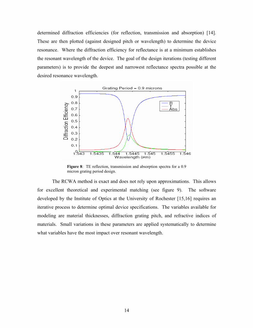


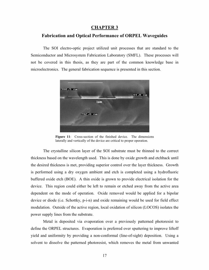


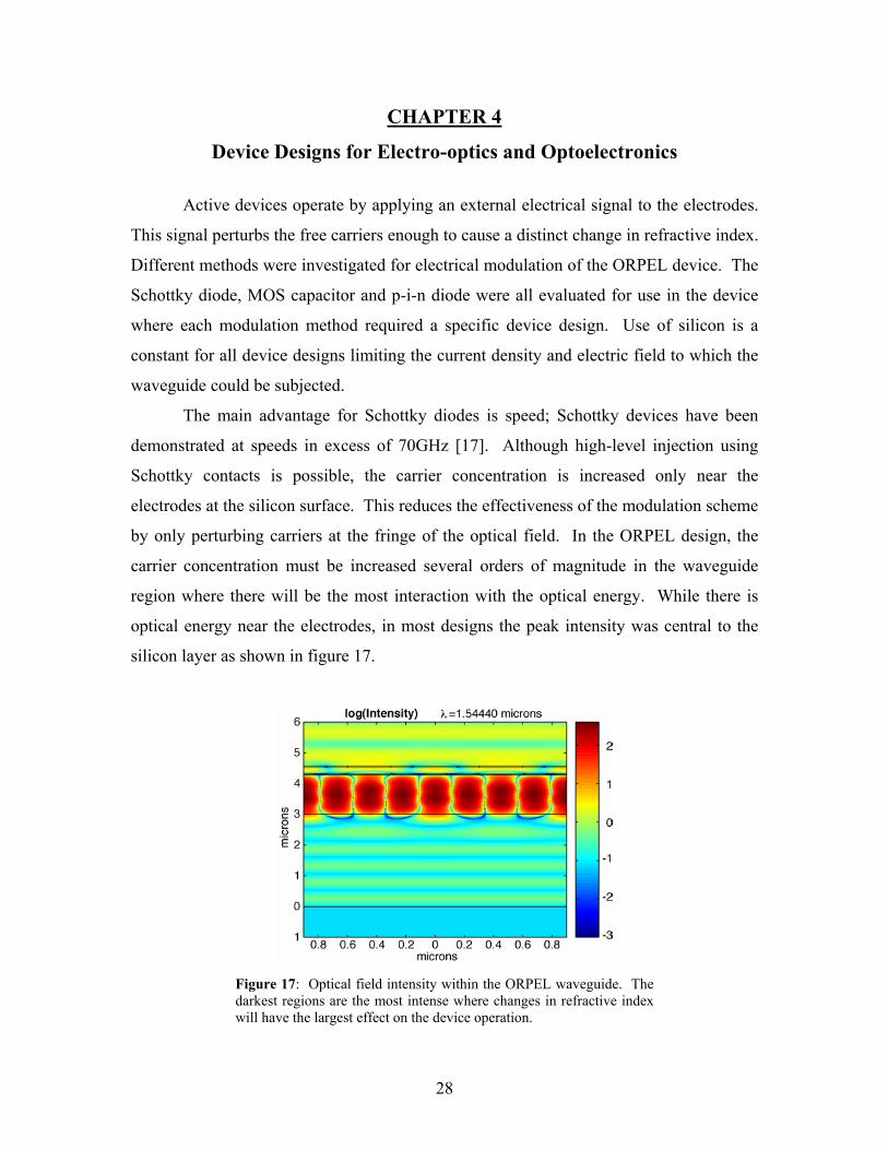


![Comparison of Slit Transmittances between Metal Plates at ...ap-s.ei.tuat.ac.jp/isapx/2016/pdf/2D3-5.pdf · Insulator-Metal (MIM) waveguide [4] with the gap width 2 g and thickness](https://static.documents.pub/doc/80x56/60665969e3b1e81a9f619b24/comparison-of-slit-transmittances-between-metal-plates-at-ap-seituatacjpisapx2016pdf2d3-5pdf.jpg)


