+ All Categories
Home > Documents > Silicon Photonics for Low- Energy Optical Communications · fds Silicon Photonics for Low- Energy...

Silicon Photonics for Low- Energy Optical Communications · fds Silicon Photonics for Low- Energy...

Date post: 20-Jul-2018
Category:
Upload: buidat
View: 223 times
Download: 0 times
Share this document with a friend
2
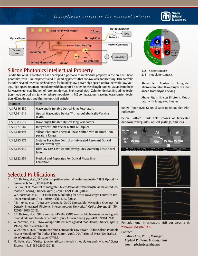
fds Silicon Photonics for Low- Energy Optical Communications To support the needs of the next generation of optical communications, researchers have developed a Sandia Silicon Photonics platform that leverages the semiconductor and nanotechnology capabilities of Sandia’s Microsystems and Engineering Sciences Applications (MESA) complex to reduce the power dissipation of interconnects within digital systems. Improving Interconnection Performance As integrated circuit chips now incorporate over a billion transistors, and single boards provide multi-teraflop (1012) computing capacity, the bandwidth and energy required to communicate data within and between integrated circuits are becoming a primary performance bottleneck. Information and communications technology (ICT) is responsible for up to 10% of US electricity consumption, with data centers responsible for about one fourth that total, and power consumption is projected to increase dramatically in the coming decades. Silicon photonics offers a potential breakthrough in optical interconnection performance, not just for supercomputer applications, but also for data communication and other applications. Importantly, silicon photonics can ride on the progress of silicon electronics and, when mature, will likely achieve the high yield, high reliability, and low costs common in the electronics industry. Enabling Power Savings Silicon photonics devices are comprised of silicon nanowire waveguides clad in silicon dioxide (SiO 2 ). The large refractive index contrast between the silicon waveguide and the oxide cladding allows light to be routed in the waveguide. Because the micro-disk resonators are so small, resonant electrically–controlled optical modulators can have capacitances as low as 20 femtofarads, and can operate with an electrical power usage of 3.2 femtojoules (fJ) per bit or lower, or 40 μW for 12.5 gigabits per second of information. This power savings is critical in high performance computing and satellite communications, especially for communications from cooled focal plane arrays. Preliminary cryogenic and radiation testing results suggest a promising future for silicon Photonics devices to operate in space. Sandia has demonstrated many leading-edge silicon photonics devices for applications in communications, sensing, and computing. In addition to the optical resonant modulator described above, we have demonstrated silicon photonics optical switching building blocks for optical networks that may enable lower energy consumption in some applications by avoiding the optical to electrical to optical conversions that are part of optically interconnected electrically routed networks. Sandia National Laboratories is a multi-mission laboratory managed and operated by Sandia Corporation, a wholly owned subsidiary of Lockheed Martin Corporation, for the U.S. Department of Energy’s National Nuclear Security Administration under contract DE-AC04-94AL85000. SAND NO. 2015-0632 C Silicon photonics offers a potential breakthrough in optical interconnection performance, not just for supercomputer applications, but also for data communication and other applications. Commercialization Path Sandia has a complete silicon photonics platform and the expertise to design silicon photonics devices for a variety of applications. We are actively seeking collaborators on photonics projects related to low-en- ergy optical communications and computing, as well as other areas of importance for national security, such as RF signal processing, quan- tum computing, secure communication, sensing, and imaging. We welcome discussions with academic and commercial entities in- terested in multi-project wafer (MPW) Si photonics fabrication runs for device prototyping and low-volume product manufacturing using our unique Si Photonics fabrication capabilities. Participants may utilize selected published Sandia photonic components in their prototypes and collaborate with our team to customize these designs or to co-develop novel concepts for their requirements. Interested parties may also col- laborate with Sandia through Cooperative Research and Development Agreement (CRADA), Funds in Agreement (FIA), and in the upcoming Integrated Photonics Institute for Manufacturing Innovation (IPIMI). Fabricated chip from multi-project wafer run for CIAN (Cornell, UCSD, UC Berkeley, and U of Arizona) Heterogeneous Integration of CMOS (top) and Silicon Photonics (bottom)
Transcript

fdsSilicon Photonics for Low-Energy Optical CommunicationsTo support the needs of the next generation of optical communications, researchers have developed a Sandia Silicon Photonics platform that leverages the semiconductor and nanotechnology capabilities of Sandia’s Microsystems and Engineering Sciences Applications (MESA) complex to reduce the power dissipation of interconnects within digital systems.

Improving Interconnection PerformanceAs integrated circuit chips now incorporate over a billion transistors, and single boards provide multi-teraflop (1012) computing capacity, the bandwidth and energy required to communicate data within and between integrated circuits are becoming a primary performance bottleneck. Information and communications technology (ICT) is responsible for up to 10% of US electricity consumption, with data centers responsible for about one fourth that total, and power consumption is projected to increase dramatically in the coming decades. Silicon photonics offers a potential breakthrough in optical interconnection performance, not just for supercomputer applications, but also for data communication and other applications. Importantly, silicon photonics can ride on the progress of silicon electronics and, when mature, will likely achieve the high yield, high reliability, and low costs common in the electronics industry.

Enabling Power SavingsSilicon photonics devices are comprised of silicon nanowire waveguides clad in silicon dioxide (SiO

2). The large refractive index

contrast between the silicon waveguide and the oxide cladding allows light to be routed in the waveguide. Because the micro-disk resonators are so small, resonant electrically–controlled optical modulators can have capacitances as low as 20 femtofarads, and can operate with an electrical power usage of 3.2 femtojoules (fJ) per bit or lower, or 40 μW for 12.5 gigabits per second of information. This power savings is critical in high performance computing and satellite communications, especially for communications from cooled focal plane arrays. Preliminary cryogenic and radiation testing results suggest a promising future for silicon Photonics devices to operate in space.

Sandia has demonstrated many leading-edge silicon photonics devices for applications in communications, sensing, and computing. In addition to the optical resonant modulator described above, we have demonstrated silicon photonics optical switching building blocks for optical networks that may enable lower energy consumption in some applications by avoiding the optical to electrical to optical conversions that are part of optically interconnected electrically routed networks.

Sandia National Laboratories is a multi-mission laboratory managed and operated by Sandia Corporation, a wholly owned subsidiary of Lockheed Martin Corporation, for the U.S. Department of Energy’s National Nuclear Security Administration under contract DE-AC04-94AL85000. SAND NO. 2015-0632 C

Silicon photonics offers a potential breakthrough in optical interconnection performance, not just for supercomputer applications, but also for data communication and other applications.

Commercialization PathSandia has a complete silicon photonics platform and the expertise to design silicon photonics devices for a variety of applications. We areactively seeking collaborators on photonics projects related to low-en-ergy optical communications and computing, as well as other areas ofimportance for national security, such as RF signal processing, quan-tum computing, secure communication, sensing, and imaging.

We welcome discussions with academic and commercial entities in-terested in multi-project wafer (MPW) Si photonics fabrication runs fordevice prototyping and low-volume product manufacturing using our unique Si Photonics fabrication capabilities. Participants may utilizeselected published Sandia photonic components in their prototypes and collaborate with our team to customize these designs or to co-develop novel concepts for their requirements. Interested parties may also col-laborate with Sandia through Cooperative Research and Development Agreement (CRADA), Funds in Agreement (FIA), and in the upcoming Integrated Photonics Institute for Manufacturing Innovation (IPIMI).

Fabricated chip from multi-project wafer run for CIAN (Cornell, UCSD, UC Berkeley, and U of Arizona)

Heterogeneous Integration of CMOS (top) and Silicon Photonics (bottom)

fds

Selected Publications:1. C.T. DeRose, et.al., “A CMOS compatible external heater-modulator,” IEEE Optical In-

terconnects Conf., 17-18 (2014). 2. J.A. Cox, et.al. “Control of Integrated Micro-Resonator Wavelength via Balanced Ho-

modyne Locking,” Optics Express, 22(9), 11279-11289 (2014).3. W.A. Zortman, et.al. “Bit-Error-Rate Monitoring for Active Wavelength Control of Res-

onant Modulators,” IEEE Micro, 33(1), 42-52 (2013). 4. A.M. Jones, et.al. “Ultra-Low Crosstalk, CMOS Compatible Waveguide Crossings for

Densely Integrated Photonic Interconnection Networks,” Optics Express, 21 (10), 12002-12013 (2013).

5. C.T. DeRose, et.al. “Ultra compact 45 GHz CMOS compatible Germanium waveguide photodiode with low dark current,” Optics Express, 19(25), pp. 24897-24904 (2011).

6. W. Zortman, et.al. “Low-voltage differentially-signaled modulators,” Optics Express, 19 (27), 26017-26026 (2011).

7. W. Zortman, et.al. “Integrated CMOS Compatible Low Power 10Gbps Silicon Photonic Heater Modulator,” in Optical Fiber Comm. Conf., OSA Technical Digest (Optical Soci-ety of America, 2012), paper OW4I.5.

8. M. Watts, et.al. “Vertical junction silicon microdisk modulators and switches,” Optics Express, 19, 21989-22003 (2011).

Silicon Photonics Intellectual PropertySandia National Laboratories has developed a portfolio of intellectual property in the area of silicon photonics, with 8 issued patents and 21 pending patents that are available for licensing. This portfolio includes several essential technologies for building low-power high-speed optical network: low-volt-age, high-speed resonant modulator (with integrated heater for wavelength tuning), scalable methods for wavelength stabilization of resonant devices, high-speed Mach-Zehnder devices (including deple-tion-mode vertical p-n junction phase-modulator in MZ configuration, traveling wave carrier deple-tion MZ modulator, and thermo-optic MZ switch).

Number Title

US 7,616,850 Wavelength-tunable Optical Ring Resonators

US 7,941,014 Optical Waveguide Device With An Adiabatically-Varying Width

US 7,983,517 Wavelength-tunable Optical Ring Resonators

US 8,027,587 Integrated Optic Vector-Matrix Multiplier

US 8,610,994 Silicon Photonics Thermal Phase Shifter With Reduced Tem-perature Range

US 8,615,173 Systems For Active Control of Integrated Resonant Optical Device Wavelength

US 8,625,939 Ultralow Loss Cavities and Waveguides Scattering Loss Cancel-lation

US 8,822,959 Method and Apparatus For Optical Phase Error Correction

Above Left: Control of Integrated Micro-Resonator Wavelength via Bal-anced Homodyne Locking

1, 2 – heater contacts 3, 4 – modulator contacts

Below Top: 45GHz Ge on Si Waveguide Coupled Pho-todetector

Below Bottom: Dark field images of fabricated nanowire waveguides, optical gratings, and lens.

For additional information, visit our website at: www.sandia.gov/mstc

Contact:Patrick Chu, Ph.D., ManagerApplied Photonic MicrosystemsEmail: [email protected]

Above Right: Silicon Photonic Modu-lator with Integrated Heater


Recommended