Louisiana Tech University Louisiana Tech Digital Commons Doctoral Dissertations Graduate School Fall 2007 Simulation and Fabrication of ree Novel Micromechanical Sensors Yanqing Lu Louisiana Tech University Follow this and additional works at: hps://digitalcommons.latech.edu/dissertations Part of the Mechanical Engineering Commons is Dissertation is brought to you for free and open access by the Graduate School at Louisiana Tech Digital Commons. It has been accepted for inclusion in Doctoral Dissertations by an authorized administrator of Louisiana Tech Digital Commons. For more information, please contact [email protected]. Recommended Citation Lu, Yanqing, "" (2007). Dissertation. 505. hps://digitalcommons.latech.edu/dissertations/505
Transcript
Louisiana Tech UniversityLouisiana Tech Digital Commons
Doctoral Dissertations Graduate School
Fall 2007
Simulation and Fabrication of Three NovelMicromechanical SensorsYanqing LuLouisiana Tech University
Follow this and additional works at: https://digitalcommons.latech.edu/dissertations
Part of the Mechanical Engineering Commons
This Dissertation is brought to you for free and open access by the Graduate School at Louisiana Tech Digital Commons. It has been accepted forinclusion in Doctoral Dissertations by an authorized administrator of Louisiana Tech Digital Commons. For more information, please [email protected].
3.2 Finite Element M odel........................................................................................................... 40
3.3 Results and Discussion.........................................................................................................46
3.3.1 Effect o f thickness o f piezoresistor on the microbridge arcuation and fractional change in resistance o f the microbridge (R/R)..................................... 46
3.3.2 Effect o f doping concentrations o f the piezoresistor on the AR/R changes 51
3.4 Fabrication o f Si0 2 microbridge with Si piezoresistors................................................53
Reproduced with permission of the copyright owner. Further reproduction prohibited without permission.
viii
CHAPTER FIVE FABRICATION AND CHARACTERIZATION OF GOLDAND PLATINUM NANOW IRES..........................................................................77
Reproduced with permission of the copyright owner. Further reproduction prohibited without permission.
LIST OF TABLES
Table 1 Common materials and their plasma etchants in dry etching [2 2 ] ..........................17
Table 2 Material properties o f Si with surface stress at [110] direction used inthe simulation.................................................................................................................45
Table 3 Material properties o f SiC>2 used in the simulation....................................................45
ix
Reproduced with permission of the copyright owner. Further reproduction prohibited without permission.
LIST OF FIGURES
Figure 1.1 Different types o f microcantilevers [4]....................................................................... 2
Figure 1.2 SEM image o f SiCh microcantilevers [6 ]....................................................................3
Figure 1.3 Microcantilever bending due to the surface stress induced by analyteadsorption [10]................................................................................................................. 4
Figure 1.4 Schematic o f an optical detection system for detectingmicrocantilever deflection [4].......................................................................................4
Figure 1.5 Application o f microcantilever-based sensors [4].................................................... 6
Figure 1.6 The process o f photolithography...................................................................................8
Figure 1.7 Four stages o f the spin-coating process [19]............................................................ 11
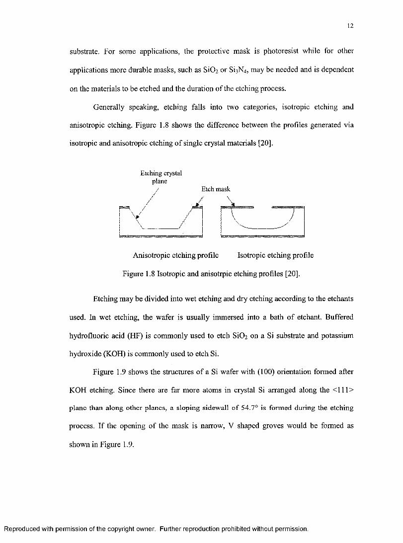
Figure 1.8 Isotropic and anisotrpic etching profiles [20].......................................................... 12
Figure 1.9 Anisotropic etching o f Si.............................................................................................. 13
Figure 1.11 Schematics o f the principle o f plasma etching [20]............................................. 15
Figure 1.12 Sketch o f an ICP coil chamber. The axial magnetic field induces anazimuthal electric field, which accelerates the charged particles [2 1 ]...............16
Figure 1.13 Schematic process o f ICP etching system [23]..................................................... 18
Figure 1.14 Lift-off procedure for patterning metal...................................................................20
Figure 1.15 Improved lift-off with two-layers o f photoresist and the bottom layerundercut.................................................................................................................................21
Figure 1.16 Typical e-beam evaporation system [24]................................................................23
Figure 1.17 The principle o f a sputtering system [25]...............................................................24
Figure 2.1 Diamond unit cell o f Si [25].................... 27
x
Reproduced with permission of the copyright owner. Further reproduction prohibited without permission.
xi
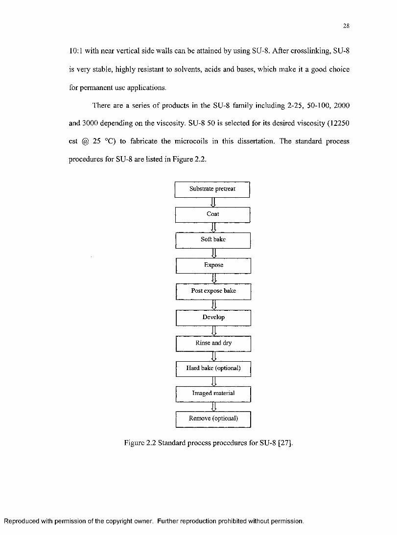
Figure 2.2 Standard process procedures for SU -8 [27]............................................................. 28
Figure 2.3 Spin-coating recipe for SU - 8 .......................................................................................29
Figure 2.4 Standard PDMS process procedures..........................................................................31
Figure 2.5 Spin-coating recipe o f PR 1813.................................................................................. 33
Figure 3.1 (a) Schematic o f the bending o f a microbridge due to analyteadsorption; (b) the microbridge under the effect o f net surface stressAg, due to physical absorption on the bridge surface and (c) theresultant arcuation o f the bridge in z direction....................................................... 38
Figure 3.2 Flowchart o f CoventorWare simulation process.....................................................43
Figure 3.3 Schematic model o f a Si covered Si0 2 microbridge..............................................44
Figure 3.4 The (a) AR/R and (b) arcuation o f Si0 2 microbridge vs. the thickness o f Si piezoresistor on the microbridge, when a surface stress o f 2 N/m was applied on the surface o f SiC>2 microbridge, c) AR/R vs. the arcuation o f the SiC>2 microbridge. The dimensions o f the SiC>2
microbridges were 400 pm in length (Lc), 50 pm in width (Wc), and 1 pm in thickness. The Si piezoresistors were 400 pm in length (Lp) and width varying from 2 pm to 10 pm. The doping concentration is lx lO 17 cm ' 3......................................................................................................................47
Figure 3.5 Effect o f (a) voltage variation, (b) temperature variation on the AR/R change o f microbridges with different thicknesses. The SiC>2
microbridges were 400 pm in length, 50 pm in width, and 1 pm in thickness. The piezoresistors were 400 pm in length, 2 pm in width, with the thickness varying from 0.2 pm to 2 pm. The doping concentration is lx lO 17 cm ' 3....................................................................................... 49
Figure 3.6 S/N ratio o f microbridges with the thickness o f the piezoresistorvarying from 0.2 pm to 2 pm. The S i0 2 microbridges were 400 pm in length, 50 pm in width, and 1 pm in thickness. The piezoresistors were 400 pm in length and 2 pm in width. The doping concentration is lx lO 17 cm ' 3..................................................................................................................50
Figure 3.7 The AR/R vs. doping concentration when a 2 N/m surface stress is applied on the surface o f an SiCh microbridge. The boron doping concentrations were from 1*1016 to 5><1019 cm 3. The dimensions o f
Reproduced with permission of the copyright owner. Further reproduction prohibited without permission.
xii
the SiC>2 microbridge were 400 pm in length, 50 pm in width, and 1
pm in thickness. The piezoresistors were 400 pm in length, 2 pm in width, and 2 pm in thickness...................................................................................... 53
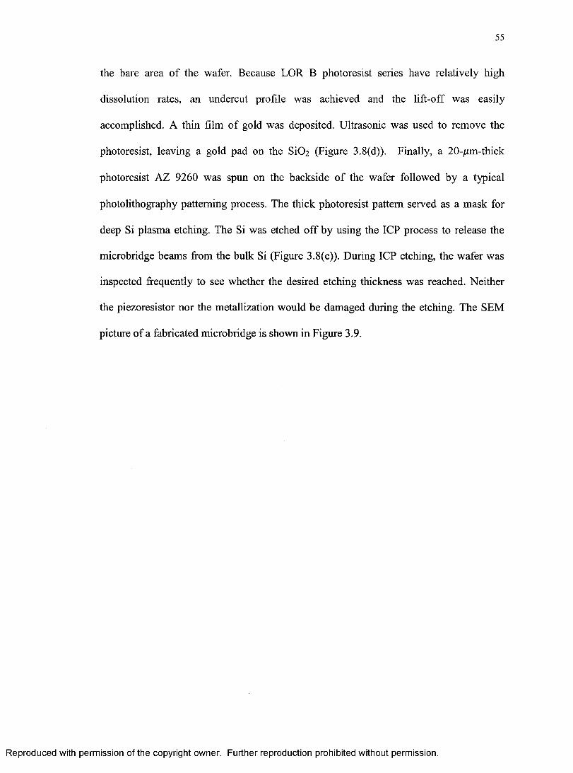
Figure 3.8 Fabrication process for SiC>2 supported piezoresistive microbridges................. 56
Figure 3.9 SEM picture o f piezoresistive Si on an SiC>2 microbridge. Thedimensions o f the SiC>2 microbridge were 400 pm in length, 50 pm inwidth, and 1 pm in thickness. The piezoresistor was 400 pm inlength, 10 pm in width, and 2 pm in thickness.......................................................57
Figure 3.10 The resistance change o f a piezoresistive Si on SiC>2 microbridge upon exposure to a 10' 6 M o f Hg2+. The dimensions o f the SiC>2
microbridge were 400 pm in length, 50 pm in width, and 1 pm in thickness. The piezoresistor was 400 pm in length, 10 pm in width, and 2 pm in thickness...................................................................................................58
Figure 4.1 The SEM picture o f a SiC>2/Si/SU - 8 trilayered microcoil and array. In the extended form, the dimensions o f the microcoil were 9.8 mm in length, 50 pm in width, and 28 pm in thickness. The coil size was 500 pm x 600 pm. The thickness o f the Si and SU-8 layer were 8 and 20 pm, respectively. For fabrication simplicity, the coil was made in a structure that the two ends o f the coil were attached to two pads outside o f the coil. To match with this structure, the specially designed SU - 8 layer was kept on the outside surfaces o f the coil in order to achieve a uniform contraction or expansion o f the coil, i.e. the SU - 8 layer from the bottom pad to the center was not connectedwith the SU - 8 from the top pad to the center.......................................................... 64
Figure 4.2 Fabrication process for the microcoils...................................................................... 6 8
Figure 4.3 Microcoils fabricated using an ICP recipe with 1800W power, 300seem SF6, 50 seem C4F8, 30W bias power and 18% pressure.............................69
Figure 4.4 Microcoil developed after (a) 120 seconds and (b) 50 secondsexposure to the UV light........................... 71
Figure 4.5 The coil movement when the inside surface is expanded (left) orcontracted (right)........................................................................................................... 72
Figure 4.6 Monolayer reaction o f APS on Si surface [92]....................................................... 73
Figure 4.7 The resistance change o f (a) an aminopropyltriethoxy-silane modified Si/SU - 8 bilayered micro-spiral spring and (b) a piezoresistive microcantilever before and after exposure to 2 .1% acetic acid in air. In the extended form, the dimensions o f the microcoil were 7.7 mm in length, 50 pm in width, and 28 pm in thickness. The dimensions
Reproduced with permission of the copyright owner. Further reproduction prohibited without permission.
o f the SiC>2 cantilever were 250 pm in length, 1 0 0 (am in width, and 1
(am in thickness. The Si piezoresistors on the SiC>2 cantilever was 100 pm in length, 20 pm in width, and 2 pm in thickness...........................................74
Figure 5.1 A schematic diagram o f the gold electrodes. The electrodes weremade on a Si wafer covered by 300-nm-thick Si(>2...............................................78
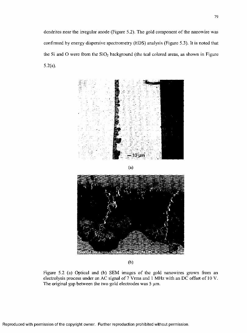
Figure 5.2 (a) Optical and (b) SEM images o f the gold nanowires grown from an electrolysis process under an AC signal o f 7 Vrms and 1 MHz with an DC offset o f 10 V. The original gap between the two gold electrodes was 5 pm......................................................................................................79
Figure 5.3 EDS analysis o f the components o f the gold nanowires and theadjacent Si0 2 surface.................................................................................................... 80
Figure 5.4 SEM images o f the platinum nanowires grown from the electrolysis process under an AC signal o f 9 Vrms and 10 Hz with an DC offset o f 13 V ..............................................................................................................................82
Figure 5.5 EDS component analysis o f the Pt nanowires......................................................... 83
Reproduced with permission of the copyright owner. Further reproduction prohibited without permission.
ACKNOWLEDGMENTS
I would like to thank my advisor, Dr. Haifeng Ji, for his invaluable advice,
continuous guidance, encouragement and support. Special acknowledgments are
extended to Mr. Ji Fang, Dr. Sidney Sit, Dr. Yuri Lvov and Dr. Tabbetha Dobbins for
their advice and serving as advisory committee members for this dissertation.
I would also like to thank the staff at Institute for Micromanufacturing (IfM),
expecially Dr. Karen Xu, Donald Tatum, Dr. Alfred Gunasekaran and John McDonald
for their help and support on the microfabrication processes as well as metrology
instruments. Much gratitude is extended to all my fellow group members for their
invaluable discussion, support, and cooperation.
Finally, I dedicate this dissertation to my family whose love and encouragement
accompanied me throughout this research.
Reproduced with permission of the copyright owner. Further reproduction prohibited without permission.
CHAPTER ONE
INTRODUCTION
1.1 Chemical and Biological Sensors
The fabrication o f the chemical and biological sensors utilizing silicon (Si)
microfabrication technologies has been the focus o f intensive research for many years
mainly because advances in technology have made mass-production and low-cost devices
possible [1], Chemical and biological sensors span a wide range o f sensor devices and
measurement instrument functionalities. Their applications include, but are not limited to,
the detection of:
1) the gross characteristics o f the overall chemical or biological environment;
2 ) the concentration or even just the presence o f particular chemical or biological
species;
3) the elemental constituents o f a mixture;
4) the molecular structure o f a pure compound or a mixture o f compounds;
5) the structure o f a bulk material and identify its atomic constituents and
three-dimensional molecular arrangements [2 ].
Among these applications o f chemical and biological sensors, one o f the most
important applications is to detect the concentration (or just the presence) o f particular
chemical or biological species, or in other words, chemical or biological sensing.
1
Reproduced with permission of the copyright owner. Further reproduction prohibited without permission.
2
Since the introduction o f the first microcantilever sensor in 1994 by Thomas
Thundat at the Oak Ridge National Laboratory (ORNL) for humidity detection [3], many
efforts have been undertaken to develop chemical and biological sensors based on
microcantilevers. The advances in microfabrication techniques has now made it possible
to mass-produce miniaturized sensors with high sensitivity.
Microcantilevers are one o f the major devices in Micro-Electro-Mechanical
Systems (MEMS). They have long, ultra thin flexible beams with tips at the front end.
Figure 1.1 shows different types o f microcantilevers [4], The typical dimensions o f the
microcantilevers are 0 .2 pm to 1 pm in thickess, 2 0 pm to 1 0 0 pm in width and 1 0 0 pm
to 500 pm in length. Si and silicon nitride (Si3N 4) are the most widely used materials for
fabricating microcantilevers [5]. In our group, silicon dioxide (SiCh) microcantilevers
have also been successfully fabricated by Y. Tang as shown in Figure 1.2 [6 ].
7
(a)
if V(b)
Figure 1.1 Different types o f microcantilevers [4],
Reproduced with permission of the copyright owner. Further reproduction prohibited without permission.
Figure 1.2 SEM image o f SiC>2 microcantilevers [6 ].
The principle o f a microcantilever is that its amplitude, frequency, deflection or
Q-factor changes due to adsorption o f chemicals on the cantilever surface or changes in
the environment [3], By monitoring the changes in the responses, humidity, viscosity,
pressure, density, temperature, flow rate, pH and the presence o f radiation in the
surrounding environment could be accurately detected [7] - [9]. The microcantilever in
Figure 1.3 [10] shows bending o f a microcantilever due to analyte adsorption induced
surface stress. The magnitude o f the bending is proportional to the concentration o f the
analyte. Figure 1.4 [4] schematically illustrates the optical approach to detect the
deflection o f a microcantilever. A laser beam from a laser diode is shined on the
microcantilever tip (usually coated with a thin layer o f gold) and is reflected o ff the
microcantilever to be received by a position sensitive photodetector. The photodetector
converts the optical signal into an electrical signal and sends it to a computer. By
Reproduced with permission of the copyright owner. Further reproduction prohibited without permission.
4
comparing the signal with a reference signal, the concentration o f the analyte could be
accurately determined.
Figure 1.3 Microcantilever bending due to the surface stress induced by analyte adsorption [1 0 ].
Figure 1.4 Schematic o f an optical detection system for detecting microcantilever deflection [4].
In general, the microcantilever technology has several advantages [4]:
> First, sensitivity. The ability to measure cantilever motion with
sub-nanometer precision allows for ppt level detection o f chemicals.
> Second, low analyte requirement. The entire sensor could fit in an area
with dimensions less than a few millimeters on a side. The corresponding
AnalyteBending
LaserDiode
LaserBeam
«PositionSensitivePhotodetector
Reproduced with permission of the copyright owner. Further reproduction prohibited without permission.
5
analyte requirement is very low due to the small size o f the
microcantilevers.
> Third, low cost. Hundreds o f microcantilevers could be fabricated on a
single wafer. Electronics for operation and control are relatively simple
and inexpensive.
> Fourth, non-hazardous procedures. It is safe to operate a microcantilever,
and there is no waste generated from the operation when compared with
traditional chemical assays.
Due to the advantages listed above, microcantilevers have been extensively
explored in their application as chemical and biological sensors, as shown in Figure 1.5
[4]. Microcantilevers can be used both in air and in solutions to detect chemical agents.
They have been investigated to detect chemical traces o f HF, Cs+, CrC>4, Ca2+ and Hg2+ in
solutions [11] - [15]. In their application as biological sensors, microcantilevers have
been used to detect DNA, antigen and biomarkers [16] - [18].
Reproduced with permission of the copyright owner. Further reproduction prohibited without permission.
6
APPLICATIONS OF MICRO CANTILEVERS FOR SENSING APPLICATIONS
Im Medicime & Biolojj'* Detection ef PSA* Detection of point mutations* Detection o f DNA & fsioteins» Detection of singt* ¥ accmta virus
piul4cks* Lab-Qfl*4»cliip* Detection of myoglobin* Blood CSucose monitoring* 'Dotedion of cells &
microorganisms* Detecting hybridisation of DNA* Detecting single base mismatches
on DNA strands* Detection atBschertehia Coti* Detection of tew-dmsdy
fy^m m s (LDLs)* lnttmehtfticid WKftte to detect
fetotofsi«l& chemise! agents* Detection of biotin & stieptevidin
In Chemistry & EnvironmentalMonitoring* Detection of temperature & heat changes* Detection of humidity• Detection of Infrared light & UV
radiations* Detection oflead & toluene in water* Detection of density/vrscosity of
dsffeftnttiquids* Detection of nerve agents namely
organophosphorous compounds* Detection of ethanol in. water* To detect electroeJje»ac#l deposition of
pcdyadlme• Detection of He* ceau«t&
caiciumions* Detection of expIoavesOoose-«n-*-diip)• To sense mechanical responses of living
cells• Toenuntna. efhactehamair• Detection of change ili pH or salt
concentration• Measure analyte vapors in the gas phase• To detect concentration of herbicides• To detect mercury vapors & merceptans* To measure changes in fluid pressure,
flow rates St sound wave velocities• Manufacture of microfabncated chip
with built-in electronic processing & telemetry
Figure 1.5 Application o f microcantilever-based sensors [4],
Inspite o f all the advantages, there still remain stability problems associated with
the microcantilevers when they are applied on a mobile vehicle or moving object, and
there is a need to improve the sensitivity o f the microcantilevers toward enhancing their
performance and applicability.
Reproduced with permission of the copyright owner. Further reproduction prohibited without permission.
7
1.2 Microfabrication Technologies
The design and fabrication o f the micro- chemical and biological sensors are
based on microfabrication technologies, which have been used for many years in the
MEMS and microelectronics fields. Microfabrication technologies originate from the
microelectronic industry, and the devices are usually made from Si, although glass,
plastics, polymers and many other materials are also in use. Si planar technology is
currently the principle processing method in the fabrication o f most Si integrated circuits
and devices, the history o f which may be dated back to 1959 when this new process was
developed at Fairchild Semiconductor.
Si planar technology is actually a collection o f technologies which are utilized in
fabricating microdevices. Basic Si planar processing steps include epitaxial growth,
Figure 1.8 Isotropic and anisotrpic etching profiles [20].
Etching may be divided into wet etching and dry etching according to the etchants
used. In wet etching, the wafer is usually immersed into a bath o f etchant. Buffered
hydrofluoric acid (HF) is commonly used to etch SiC>2 on a Si substrate and potassium
hydroxide (KOH) is commonly used to etch Si.
Figure 1.9 shows the structures o f a Si wafer with (100) orientation formed after
KOH etching. Since there are far more atoms in crystal Si arranged along the <111>
plane than along other planes, a sloping sidewall o f 54.7° is formed during the etching
process. If the opening o f the mask is narrow, V shaped groves would be formed as
shown in Figure 1.9.
Reproduced with permission of the copyright owner. Further reproduction prohibited without permission.
13
F7\
ZZI 1Z
(a) top view
54.7°
(b) side view
Figure 1.9 Anisotropic etching o f Si.
Although wet etching has been extensively used in microfabrication, it has many
problems. The capillary action o f wet etching would cause penetration o f the etchant
under the mask and result in ragged edges. Also, large amounts o f waste products are
produced during the wet etching process, thus being environmentally undesirable.
As an alternative to wet etching, dry etching usually employs a gas to either
physically bombard or chemically react with the target to remove the unwanted part o f
the patterned wafer. Dry etching is highly directional. Anisotropic etching can be
obtained by adjusting dry etching parameters such as flow rate, pressure and power.
Another advantage o f dry etching compared with wet etching is that it is more
environmentally desirable since it doesn’t produce as much waste products.
In IfM, dry etching is usually done via Inductively Coupled Plasma (ICP, Alcatel
601E) as shown in Figure 1.10 and Deep Reactive Ion Etching (DRIE). ICP etching was
used extensively to fabricate the microbridge and microcoil structures for this work. The
following section in this chapter describes dry etching in detail, since it is one o f the most
important steps used in fabricating the micro devices in this dissertation.
Reproduced with permission of the copyright owner. Further reproduction prohibited without permission.
14
Figure 1.10 Alcatel 60IE ICP equipment.
Plasma, by its nature, is a highly ionized gas. It is composed o f ionized particles
with positive or negative charges but is neutral as a whole. This property makes it
chemically highly reactive and very useful in microfabrication for etching materials. In
dry etching, plasma is usually produced from a gas by applying electromagnetic
excitation. Figure 1.11 is a schematic picture illustrating the principle o f plasma etching.
Reproduced with permission of the copyright owner. Further reproduction prohibited without permission.
Before etching End of etchingMask
Bulk,wafer
Figure 1.11 Schematics o f the principle o f plasma etching [20].
As can be seen from Figure 1.11, the top electrode o f the plasma etcher is
connected to the RF source with a frequency o f 13.56 MHz, which is internationally
assigned for plasma etching equipment usage. By the excitation o f the RF power, the
gases in the chamber o f the system are ionized and bombard the target wafer positioned
on the bottom electrode. At the bottom o f the system, the gas evacuation holes remove
the gaseous wastes from the chamber, thus sustaining the progress o f the etching. In
DRIE, a variation o f plasma etching, plasma is generated by a magnetic field, and then
Reproduced with permission of the copyright owner. Further reproduction prohibited without permission.
16
densified by a second magnetic field generator. The objective is to reach a high ionization
rate in the gases to enhance the etching effect [21].
In an Inductively Coupled Plasma system (ICP) as shown in Figure 1.12 [21], a
coil surrounding the reaction chamber generates a magnetic and azimuthal electrical field.
This electrical field accelerates the plasma to bombard and react with the wafer. Due to
the magnetic field, the inductive coupling method produces a very dense plasma. The
ability to form very dense plasmas and, at the same time, control the ion bombardment o f
the substrate, enables ICP etching to have high etching rates with high mask selectivities.
RFcdlMatching unit
RF Generator
Water
SubstrateSub. holder
End plate
To pump
Water in
Bias
Figure 1.12 Sketch o f an ICP coil chamber. The axial magnetic field induces an azimuthal electric field, which accelerates the charged particles [21].
Reproduced with permission of the copyright owner. Further reproduction prohibited without permission.
17
There are different gas sources for etching different materials. Table 1 [22] lists
the plasma etchants for common materials in microelectronics and microfabrication, such
as Si, Si02, Si3N4, organics and aluminum.
Table 1 Common materials and their plasma etchants in dry etching [22]
Materials to be Etched Etchant gasSi c f 4, s f 6
S i0 2 c f 4/h 2Si3N4 c f 4/o 2
Organics o 2, o 2/ c f 4, o 2/ s f 6Aluminum b c i3
CF4 and SF6 have been generally used in Si plasma etching, as can be seen from
Table 1. The chemical reaction for Si dry etching is shown in Equation 1.1,1.2 and 1.3.
CF4 + e' -*• CFX. + CF. + F. +e' (1.1)
nCFx. -* nCF2(ads)-> nCF2(f) (1.2)
nCF2(f)+ F. -* ion energy -> CFx(ads) CFx(g) (1.3)
After CF4 is admitted into the ICP system, it is dissociated into ions and radical
species as shown in Equation 1.1. CFX. then goes though polymerization reactions to form
nCF2(f), the passivation layer to be deposited on the sidewall and surface o f the Si
(Equation 1.2). Then, CF4 is turned o ff andSF6gas is admitted, the dissociation o f which
would introduce fluorine radicals to remove the surface passivation layer (Equation 1.3).
Figure 1.13 illustrates schematically the reactions occurring in the ICP system.
Reproduced with permission of the copyright owner. Further reproduction prohibited without permission.
18
fluorinatedpolymer
Si
SiO,
Si
Si
■
(a) Passivating layer is deposited on the surface o f the silicon and the mask
(b) Fluorine radicals remove the surface passivation
SFfi
(c) Fluorine radicals etch silicon
Figure 1.13 Schematic process o f ICP etching system [23].
1.2.4 Metallization
Interconnections between devices and the outside world are realized by
conductive films in microfabrication and microelectronics. Aluminum and gold are
currently the two most widely used metals. The advantages o f these metals are listed
below. First o f all, they are able to withstand high current densities without
Reproduced with permission of the copyright owner. Further reproduction prohibited without permission.
19
electromigration or material failure. Secondly, low-temperature deposition techniques are
available for both aluminum and gold. Thirdly, they adhere to the substrate more easily.
Fourthly, good ohmic contact can be made with aluminum and gold to both p- and n-type
Si. Lastly, and most important o f all, they are easy to be patterned and etched and are
reliable throughout long-term operation. Gold is used in the fabrication discussed in this
work.
Although gold can be etched in aqua regia (HC1:HN0 3 in a 3:1 ratio by volume),
this approach is not desirable since it destroys most resist and metal mask materials. In
industry, a commonly adopted way to etch gold is to use a dilution o f KI and iodine in
water. In the fabrication o f the microbridge and microcoils, gold is patterned through a
procedure called lift-off.
Lift-off is a simple and easy method for patterning metal thin films on a Si wafer
surface. A simple schematic o f the lift-off process is shown in Figure 1.14. The first step
for lift-off is to pattern the wafer by standard lithographic techniques so that photoresist
covers the regions where metal is not needed. By blanket-deposition o f the desired metal
over the entire substrate surface, including both photoresist covered areas and bare Si
areas, a thin film o f the metal is formed uniformly on the substrate. The metal thus
contacts the substrate only in areas where it is needed. By soaking the wafer in a solvent
to remove the photoresist, only the metal on the desired areas is left on the wafer surface
while the rest o f the metal is lifted o ff together with the photoresist beneath it. Ultrasonic
is usually used during lift-off to promote the strip o f the photoresist (and the metal above
it) from the wafer substrate.
Reproduced with permission of the copyright owner. Further reproduction prohibited without permission.
Wafer with patterned photoresist
Deposited metal
Strip photoresist and lift o ff unwanted metal
Figure 1.14 Lift-off procedure for patterning metal.
A potential problem with the lift-off procedure shown above is that the thin metal
film deposited on the sidewall o f the photoresist will stay on the substrate after the
photoresist removal. The sidewall might be peeled o ff in subsequent processing, resulting
in particulates and shorts on the substrate and affecting the processes that follow. An
improved lift-off procedure is presented in Figure 1.15 by utilizing a two layer
photoresist system with different etch rates. Since the etch rate for the bottom layer
(usually LOR-7B) is faster than the top layer, the bottom photoresist is slightly undercut
thus makes it easier to lift o ff the photoresist.
Reproduced with permission of the copyright owner. Further reproduction prohibited without permission.
21
• « ih •
LOR 7B coated
Photoresist (PR1813) coated
1 ---------
Development
Metal Deposition
Lift-off
Figure 1.15 Improved lift-off with two-layers o f photoresist and the bottom layer undercut.
1.2.5 Oxidation
Si02 has many applications in microfabrication and microelectronics. It can serve
as a mask for diffusion and ion implantation, as a gate dielectric film, and as passivation
layers, protecting the Si from contamination during subsequent processing steps. Upon
exposure to air, the surface o f Si is naturally oxidized and covered with a 15-20 A thick
layer o f native Si0 2 -
During controlled oxidation, the Si wafers are placed in a furnace while oxygen
gas (dry oxidation) or steam (wet oxidation) is flowing across them. In order to grow a
layer o f SiC>2 on a wafer in an acceptable amount o f time the process has to be done at
very high temperatures between 700°C and 1300°C. The thermal oxidation o f Si
Reproduced with permission of the copyright owner. Further reproduction prohibited without permission.
22
conducted in quartz furnace tubes allows relatively dense, adherent, trap-free layers o f
S i0 2 to be grown with ease.
Si is oxidized at its surface. The oxidizing species must therefore diffuse through
the growing oxide layer in order to combine with the Si atoms at the wafer surface. The
chemical reactions o f Si with oxygen and water vapor are summarized respectively as
shown in Equation 1.4 and Equation 1.5 below.
Si + 0 2 -*• S i0 2 (1.4)
Si + 2 H20 -> S i0 2 + 2 H2 (1.5)
1.2.6 Thin Film Deposition
There are three primary ways for thin-film deposition, which are evaporation,
sputtering and chemical vapor deposition. The following section discusses electron beam
evaporation and sputtering, two deposition techniques used in the fabrication in this
work.
The e-beam evaporator is used to evenly coat samples with metals. It is usually
used when the required temperatures for the deposition o f certain metals are too high for
thermal evaporation. It is good for titanium, chrome, platinum or gold films deposition.
In the evaporation process, the material (source) to be deposited is heated to the
temperature where it liquefies and starts to evaporate. Then it is allowed to condense on
the substrate. In a typical process the chamber is pumped down to a pressure o f 5 x 10'6
torr to prevent air molecules from interfering with the deposition as well as allowing the
molecules to evaporate freely from the source. A high-intensity electron beam gun (3 to
20keV) is focused on the source and causes the metal to evaporate and thus be deposited
on the substrate. Typical deposition rates range from 1 to 5 A/second. Figure 1.16
Reproduced with permission of the copyright owner. Further reproduction prohibited without permission.
23
illustrates the schematic diagram o f a typical e-beam evaporation system.
.Wafer caroussel
Material to be evaporated
Thermoionic flamemt
Water-cooled crucible
Figure 1.16 Typical e-beam evaporation system [24].
Sputtering is a technology in which the sputtered material is released from the
source at much lower temperature than evaporation. It is more versatile than evaporation,
and is extensively used in microfabrication. In a sputtering system, as shown in Figure
1.17 [25], the substrate is placed in a vacuum chamber with the source material, and an
inert gas (such as argon) is introduced at low pressure. The gas is ionized using an RF
power source. The ions are accelerated towards the surface o f the target, causing atoms o f
the source material to be ejected from the target and deposited on the substrate.
Reproduced with permission of the copyright owner. Further reproduction prohibited without permission.
24
SubstrateTable
Argon/OxygenPlasma
VacuumChamber
RFGenerator
T arget
MatchingN̂etwork
GroundedShield
Figure 1.17 The principle o f a sputtering system [25],
1.3 Research Objectives
Design and fabrication o f highly sensitive chemical and biological sensors is o f
great interest to a number o f researchers. There are still enough opportunities for
microsensors to be improved with optimized stmctures, enhanced sensitivity and new
materials, as well as enhanced performance.
The objective o f this research is to design and develop new chemical and
biological sensors based on Si microfabrication technologies. Specifically, piezoresistive
microbridges and microcoils have been selected as the microsensors to be designed and
fabricated due to their high sensitivity and stability. The materials used for the fabrication
o f the microsensors were Si, SiC>2 and SU-8. Before the fabrication, the microsensors
were simulated via Finite Element Analysis software to determine the optimized size and
design for the structures. Standard Si fabrication techniques, including spin-coating,
lithography, wet and dry etching and lift-off, were used to fabricate the microsensors.
After the fabrication, the sensors were characterized by exposing them to a real
environment to test their performance.
Reproduced with permission of the copyright owner. Further reproduction prohibited without permission.
25
1.4 Dissertation Outline
There are six chapters in this dissertation. The first chapter overviews chemical
and biological sensors and their applications followed by an introduction to the
microfabrication technologies as well as the objective o f this dissertation. The second
chapter describes the materials used in the fabrication o f the microsensors and the
measurement instruments and techniques for device characterization. Chapter three
focuses on the simulation, fabrication and characterization o f the microbridge sensors.
Chapter four describes the principle, the fabrication and the characterization o f the
microcoil sensors. Chapter five is focused on a new approach to grow gold and platinum
nanowires. The last chapter concludes this dissertation and discusses the prospects for
future work that still needs to be done.
Reproduced with permission of the copyright owner. Further reproduction prohibited without permission.
CHAPTER TWO
EXPERIMENTAL MATERIALS
AND EQUIPMENTS
Si is the most widely used material in microfabrication. Si and its physical
properties are the basis for subsequent microfabrication processing. This chapter presents
the structure o f Si and its corresponding properties. Other materials used in this work,
including SU-8, PDMS, Shipley 1813 are also introduced. The principles o f metrology
instruments used for device characterization, including SEM, AFM, and surface
profilometer, are briefly discussed in this chapter.
2.1 Experimental Materials
2.1.1 Si
Si is so far the most widely used material for microfabrication and
microelectronics. A brief introduction on the atomic structure o f Si and its physical
properties would help to understand the corresponding fabrication techniques and the
physics o f Si devices.
Si is a crystalline solid. Its atoms are organized in an orderly array, as shown in
Figure 2.1. The diamond lattice structure, the smallest assembly o f atoms that can be
repeated to form crystalline Si is called the unit cell.
26
Reproduced with permission of the copyright owner. Further reproduction prohibited without permission.
Figure 2.1 Diamond unit cell o f Si [25].
Piezoresistivity is a very important property o f Si. It has been reported that the
resistivity o f a material depends on the internal atom positions and their motions [26]. By
applying strain or stress to a material, the atomic positions o f the material would be
changed. This change would cause the energy band to shift compared to the stress-free
state. Thus, in some directions o f the material, the resistivity would be larger while in
other directions the resistivity would be smaller. The overall resistivity o f the material
will change after a strain or stress is applied and the change o f the resistivity is related to
the magnitude o f the applied strain or stress. More details o f the piezoresistive properties
o f Si w ill be covered in chapter 3. The designs o f the microbridge and microcoil sensors
are all based on the piezoresitive property o f Si.
2.1.2 SU -8
SU-8 is used in the fabrication o f the microcoil, standing side by side with the Si
microcoil. SU-8 is a high contrast, epoxy based negative photoresist designed for
micromachining and other microelectronic applications. High aspect ratios larger than
Reproduced with permission of the copyright owner. Further reproduction prohibited without permission.
10:1 with near vertical side walls can be attained by using SU-8. After crosslinking, SU-8
is very stable, highly resistant to solvents, acids and bases, which make it a good choice
for permanent use applications.
There are a series o f products in the SU-8 family including 2-25, 50-100, 2000
and 3000 depending on the viscosity. SU-8 50 is selected for its desired viscosity (12250
cst @ 25 °C) to fabricate the microcoils in this dissertation. The standard process
procedures for SU-8 are listed in Figure 2.2.
Coat
Rinse and dry
Hard bake (optional)
Imaged material
Expose
Substrate pretreat
Develop
Remove (optional)
v ___Soft bake
Post expose bake
Figure 2.2 Standard process procedures for SU-8 [27].
Reproduced with permission of the copyright owner. Further reproduction prohibited without permission.
29
Prior to spin-coating SU-8 on the Si wafer, the surface o f the wafer should be
cleaned by acetone spray to remove organic contaminants. Then the wafer should be
dried on a hot plate at 500 °C for 5 minutes.
The spin-coating recipe, as illustrated in Figure 2.3, is adopted to obtain a 50 fim
thick SU-8 film. The spinner is first ramped to 500 rpm at 100 rpm/second acceleration.
This speed is held for 5 seconds to allow the resist to cover the entire surface. Then the
spinner is ramped to the final speed o f 1000 rpm at an acceleration speed o f 300
rpm/second and held for a total o f 40 seconds [27],
1200
1000
800
600rpm
400
200
0 5 10 15 20 25 30 35 40 45 50
time (seconds)
Figure 2.3 Spin-coating recipe for SU-8.
The next step is soft bake, the purpose o f which is to evaporate the solvent and
densify the film. Soft bake is conducted at 65 °C for 10 minutes and then stepped to 95
°C for 30 minutes. The stepped soft bake temperatures are used to allow the solvent to
Reproduced with permission of the copyright owner. Further reproduction prohibited without permission.
30
evaporate from the film at a more controlled rate thus achieving better coating
uniformity, reduced edge bead and better resist-to-substrate adhesion [27].
After soft bake, the SU-8 thin film is exposed to near UV (365nm) exposure for
50 seconds. Underdevelopment would cause the desired SU-8 to be etched away while
overdevelopment would result in problems in development.
Following exposure, post exposure bake must be performed to further cross link
the exposed portions o f the film. As with soft bake, post bake is also performed using a
stepped temperature cycle. The reason this is done is to minimize film stress and resist
cracking problems. One minute bake at 65 °C is followed by an 8 minute bake at 95 °C
for 50 /xm thick SU-8 film.
After post exposure bake, the wafer, covered with SU-8 film, should be soaked in
SU-8 developer to dissolve away non-exposed SU-8 and selectively leave crosslinked
SU-8 on the wafer. This procedure, in practice, lasts for about 6 minutes for 50 /xm thick
SU-8.
Subsequent processing steps include rinsing the wafer with isopropyl alcohol
(IPA) to remove resist residue, rinsing the wafer with DI water to clean the wafer,
blowing dry the wafer with nitrogen gas and an optional hard bake at 200 °C to further
crosslink the SU-8.
The SU-8 used in the fabrication o f the microcoil in this dissertation is
commercially available from Microchem.
2.1.3 PDMS
Polydimethylsiloxane (PDMS) is widely used as a Si-based organic polymer, and
is known for its unusual flow properties. It is optically clear, very viscous, inert,
Reproduced with permission of the copyright owner. Further reproduction prohibited without permission.
31
non-toxic and non-flammable. Standard PDMS process procedures are listed in Figure
2.4.
Blend base and curing agents
___________ SZ______________Pour onto a substrate
___________ SZ_________________Remove bubbles in a vacuum oven
Cure in an oven
________________SZ________________Peel off from the substrate
Figure 2.4 Standard PDMS process procedures.
SYLGARD 184 was purchased from Dow Coming (Midland, MI). SYLGARD
184 consists o f a “base” (prepolymer) and “curing agent” (crosslinker) that need to be
mixed thoroughly at a 10:1 w/w ratio. After the base and the curing agent are mixed and
then transferred onto a substrate such as a Si wafer, they are degassed in a vacuum oven
for 30 minutes to remove any bubbles generated during mixing. Then PDMS is cured at
95 °C for 2 hours or overnight at 60 °C. The last step is to peel o ff the PDMS from the
substrate after the PDMS is cooled down to room temperature. Care must be taken to
keep the PDMS film from being tom. The thickness o f the PDMS obtained following
above procedures is around 500 pm. By using a container to encase the substrate and
prevent the PDMS from flowing off the substrate, thicker PDMS can be obtained.
Reproduced with permission of the copyright owner. Further reproduction prohibited without permission.
32
2.1.4 PR1813
Shipley 1813 positive tone photoresist (PR1813) has been widely used as a
positive photoresist for pattern transfer from the mask to the wafer. It is UV curable and
solvent soluble, and very easy to handle. To spin coat PR1813 onto a wafer, the following
steps are followed,
> First, center the wafer on the spinner.
> Second, transfer PR1813 from the container to the wafer with a pipette.
> Third, ramp the spin coater first to 1000 rpm at 100 rpm/second
acceleration. Hold at this speed for 10 seconds to allow the resist to cover
the entire wafer surface.
> Fourth, ramp the spin coater to 3000 rpm at 500 rpm/second acceleration.
Hold at this speed for a total o f 40 seconds. Figure 2.5 shows the
spin-coating recipe for PR-1813.
> Fifth, soft bake the wafer at 110 °C for 1 minute to evaporate the solvent
and dry the film.
> Sixth, expose the wafer to UV light through a mask for 8 seconds.
> Seventh, develop the wafer in Microposit Developer for about 45 seconds.
Inspect the pattern frequently during the development to see if it is etched
properly.
> Eighth, bake the wafer at 115 °C for 1 minute to further dry the film and
prevent reflowing.
Reproduced with permission of the copyright owner. Further reproduction prohibited without permission.
33
3000 -|
2500 -
2000 -
1500 -rpm
1000 -
500 -
0 5 10 15 20 25 30 35 40 45 50 55 60
time (seconds)
Figure 2.5 Spin-coating recipe o f PR 1813.
2.2 Experimental Equipment
2.2.1 SEM
Compared to an optical microscope which utilizes visible light to create
magnified images o f a sample surface, the scanning electron microscope (SEM) is an
electron microscope using electrons to produce high-resolution images. The images taken
by SEM have a characteristic three-dimensional appearance and can show very detailed
information o f the sample surface.
In the SEM, electrons are emitted from the cathode and are accelerated towards
the anode. When the primary electron beam interacts with the sample, the electrons lose
energy and generate secondary electrons, backscattered electrons, and characteristic
X-rays. By detecting these signals, images on the sample surface can be formed and
Reproduced with permission of the copyright owner. Further reproduction prohibited without permission.
34
displayed on a cathode ray tube screen. Features as small as 5 nm can be detected by
SEM.
Figure 2.6 illustrates the SEM (Amray 1830) used for this work. It has two major
parts, the electron optical column console and the electronics and display console.
Figure 2.6 Amray 1830 SEM.
2.2.2 AFM
The atomic force microscope (AFM) uses a sharp probe to detect surface features
on a sample. It is possible to image the surface topography o f an object with extremely
high resolution with the AFM. A schematic o f the principle o f operation o f the AFM is
shown in Figure 2.7 [28].
Reproduced with permission of the copyright owner. Further reproduction prohibited without permission.
35
S 4
f i(a)
(b)
Figure 2.7 (a) Operating principle o f the AFM and (b) the tip o f the AFM [28].
The key part o f the AFM is a small microcantilever with a very sharp tip at the
end (Figure 2.7 (b)). When the tip scans over the surface o f a sample, interatomic forces
between the cantilever tip and the sample surface cause the cantilever to be deflected as
the surface topography o f the sample changes. This deflection causes a deflection o f the
laser beam, which is reflected o ff the cantilever beam, and is detected by a photodetector.
Thus, any change in the surface topography is converted into electrical signals and a map
o f the sample topography can be generated.
Reproduced with permission of the copyright owner. Further reproduction prohibited without permission.
36
The advantage o f the AFM is that it provides a true three-dimensional surface
profile o f a sample, and it can, in principle, provide higher resolution than the SEM.
2.2.3 Surface Profilometer
Step height needs to be checked from time to time during the process o f
microfabrication. A profilometer works to fulfill this purpose. A profilometer usually has
a diamond stylus that scans over the surface o f the sample. A surface profile over a
specified range could be generated by recording the displacement o f the diamond stylus
versus the position scanned. Step heights and surface roughness o f the sample substrate
can be determined from the profile. Figure 2.8 shows the profilometer used for this work
(KLA Tencor Profilometer).
Figure 2.8 KLA Tencor profilometer.
Reproduced with permission of the copyright owner. Further reproduction prohibited without permission.
CHAPTER THREE
SIMULATION AND FABRICATION
OF MICROBRIDGES
3.1 Introduction
Advances in the field o f micro- and nano-electro-mechanical systems (MEMS and
NEMS) now offer unique opportunities in the design o f small and ultrasensitive micro
sensors. Microcantilevers have proven to be an outstanding platform for chemical and
biological sensors. The unique characteristic o f microcantilevers is that the device can be
made to undergo bending due to molecular adsorption by confining the adsorption to one
side o f the cantilever. This bending is due to adsorption-induced differential stress on the
cantilever.
The challenge associated with the microcantilever is the stability o f the cantilever
when the device is used on a mobile vehicle or moving object. It appears that a
microbridge d ev ice w ill overcom e the stability problem associated w ith the
microcantilever. A microbridge can be considered as the head-to-head fusion o f two
cantilevers where the middle o f the bridge would deform in a way similar to a
microcantilever due to molecular adsorption upon exposure to the analyte (Figure 3.1(a)).
Reproduced with permission of the copyright owner. Further reproduction prohibited without permission.
38
It is anticipated that this microbridge sensing device will be more stable than the
microcantilever, especially in turbulent or vibrant conditions. The trade-off might be the
low AR/R change o f the microbridge compared to that o f the microcantilever.
Figure 3.1 (a) Schematic o f the bending o f a microbridge due to analyte adsorption; (b) the microbridge under the effect o f net surface stress Acr, due to physical absorption on the bridge surface and (c) the resultant arcuation o f the bridge in z direction.
Microbridges, based on the principle o f electrostatic excitation and capacitive
detection, have been used as integrated chemical vapor sensors for sensing gas
composition o f binary mixtures [29] - [33]. Various transduction mechanisms have been
developed to detect the resonance frequency changes o f microbridges. These mechanisms
include the piezoresistive approach based on polysilicon peizoresistors [33] - [38], the
piezoelectric approach with piezoelectric (PZT) materials, such as ZnO [39] - [41], and
(a)Z
tGT“
(b)
**
(c)
Reproduced with permission of the copyright owner. Further reproduction prohibited without permission.
39
the optical approach using laser light to measure the frequency change or displacement
movement [42] - [44]. These microbridges are sensitive transducers that provide the basis
for mass [45] - [47], temperature [48], [49], strain [50], acceleration [51], and vibration
sensors [52].
Microbridges have been fabricated from Si [34], [36] - [38], [46], [53] - [55],
Thinkness of the p iezoresisto rs , pm Arcuration, pm
(b) (c)
Figure 3.4 The (a) AR/R and (b) arcuation o f SiC>2 microbridge vs. the thickness o f Si piezoresistor on the microbridge, when a surface stress o f 2 N/m was applied on the surface o f SiCb microbridge. c) AR/R vs. the arcuation o f the SiC>2 microbridge. The dimensions o f the SiC>2 microbridges were 400 pm in length (Lc), 50 pm in width (Wc), and 1 pm in thickness. The Si piezoresistors were 400 pm in length (Lp) and width varying from 2 pm to 10 pm. The doping concentration is lx lO 17 cm'3.
Reproduced with permission of the copyright owner. Further reproduction prohibited without permission.
48
It has been reported that the AR/R change is directly proportional to the
microcantilever bending [74]. Our simulation results suggest that a similar relationship
could be used to correlate the AR/R change with arcuation o f the microbridges, although
no equations have been developed in the literature.
The AR/R keeps increasing when the thickness decreases. The optimized
thickness for chem/bio sensing, however, will be obtained from noise optimization.
Piezoresistive sensors have two main possible noise sources, thermal and Hooge noise,
which are generated from temperature and voltage variations, respectively [75]. Larger
noise will lower the signal/noise (S/N) ratio, and thus the sensitivity. The S/N ratio under
temperature and voltage variations could be used to optimize the thickness o f the
piezoresistive microbridge. Figure 3.5 (a) shows that a 100% voltage variation does not
change the AR/R o f the microbridge. However, a 0.3% temperature variation, as shown in
Figure 3.5 (b), generates significant noise, especially when the Si piezoresistor is thinner
than 1 fim. Figure 3.5 (b) inset shows the resistance change noise due to the 0.3%
temperature variation (defined as ^ ̂̂ ook / R 299K) thermal noise o f the
resistors increased approximately 5-fold when the thickness decreases from 2 /xm to 0.2
jam.
Reproduced with permission of the copyright owner. Further reproduction prohibited without permission.
49
0.0014
A pplied v o lta g e0.0012
- A - 4 V —V— 2 V0.0010
£ 0.0008
0.0006
0.0004
0.00020.5 1.0 1.5 2.0
Thickness of the piezoresistors, pm
(a)
0.00146e-5
S 5e-5 ofS 4e-5
J 3e-5
0.0012
0.0010< 2e-5
1e-5£ 0.0008 0.5 1.0 1.5 2
Thickness of Si, pm
0.0006
T e m p e ra tu re
299 K300 K
0.0004
0.00020.5 1.0 1.5 2.0
Thickness of the piezoresistors, pm
(b)
Figure 3.5 Effect o f (a) voltage variation, (b) temperature variation on the AR/R change o f microbridges with different thicknesses. The SiC>2 microbridges were 400 pm in length, 50 pm in width, and 1 pm in thickness. The piezoresistors were 400 pm in length, 2 pm in width, with the thickness varying from 0.2 pm to 2 pm. The doping concentration is lx lO 17 cm'3.
Reproduced with permission of the copyright owner. Further reproduction prohibited without permission.
50
From those data in Figure 3.5 (b) and Figure 3.5 (b) inset, the S/N ratio o f the
microbridges at different thicknesses were calculated and shown in Figure 3.6. These
results suggest that although the AR/R o f the microbridge increases when the thickness
decreases, the S/N ratio does not change significantly from 2 pm to 0.2 pm thickness, i.e.
when the temperature variation is controlled to 1 K, the thickness o f the Si piezoresistor
does not play a critical role in obtaining the best S/N ratio.
When simulated and compared to microcantilevers with the same dimensions, the
AR/R change o f the microbridge is approximately 1/3 o f that o f the microcantilever, and
the microbridge is approximately 50% more temperature dependent than the
microcantilever.
25
Zto
0.2 0.4 0.6 0.8 1.0 1.2 1.4 1.6 1.8 2.0
Thinkness of the piezoresistors, pm
Figure 3.6 S/N ratio o f microbridges with the thickness o f the piezoresistor varying from 0.2 pm to 2 pm. The S i0 2 microbridges were 400 jam in length, 50 jam in width, and 1
/am in thickness. The piezoresistors were 400 /am in length and 2 /am in width. The doping concentration is lx lO 17 cm'3.
Reproduced with permission of the copyright owner. Further reproduction prohibited without permission.
51
3.3.2 Effect o f doping concentrations o f the piezoresistor on the
AR/R changes
The resistance change o f a piezoresistor (AR/R) after a stress is applied can be
expressed as shown in Equation 3.2.
where R is the resistance o f the stress-free piezoresistor, nt , <J, and nt , o t refer to
the piezoresistive coefficient and stress along the longitudinal and traverse direction with
respect to the resistor axis, respectively.
nl and n t can be expressed as follows,
where (//, m /,«/) and (l2, m2, n2) are the sets o f direction cosines between the longitudinal
resistor direction and the crystal axis, and between the transverse resistor direction and
the crystal axes [76].
For piezoresistors oriented along the [110] direction in (100) wafers, (l\, m\, n\)
and {h, m2, n2) are ( l/V 2 , 1/V 2 , 0) and ( -1/>/2 , l/V 2 , 0) respectively. Inserting these
values into Equation (3.3), we have,
AR- XiCJ, + 7Ct(J t (3.2)
n, =7tu ~ 2 { k u - j i n - 7 i ^ ) { l 2m 2 + l 2n 2 + m * n 2)
f t t ~ f t 12 ( f t n f t \ 2 ^ 4 4 X A 12 m \ m 2 "*■ n \ n 2 ) (3.3)
Ki ~ 2 ^ u +7Cn
ftt ~ —(ftn +ft\2 ~ f t ^ ) (3.4)
Reproduced with permission of the copyright owner. Further reproduction prohibited without permission.
52
Since the length o f the microbridge is much longer than its width and the surface
stress is along the x axis, the microbridge can be seen as a 1-D device and Equation (3.2)
could be reduced to Equation (3.5)
— = n p , (3.5)
At low doping concentrations (<5 x 1014 cm’3), the piezoresistive coefficient in the
[110] direction for p-type Si is a constant at 7 2 x l0 _11»i2 / A [76]. Numerous reports
showed that when the doping concentration is increased, the piezoresistive coefficient
n, is decreased [77]. The model developed by Kanda [78] is accurate only for low
doping concentrations. A piezoresistive factor P ( p ) was defined to express the
coefficients as a fraction o f this maximum value by the approximation Equation (3.6) for
concentration above 1 0 17 cm"3.
P (p ) = Log\ P j (3.6)
99 3where a = 0.2014, b = 1.53* 10 cm" andp is the doping concentration.
The Piezoresistive factor P (p ) is directly related to n l by Equation (3.7) [15].
n l{ N J ) = P { p ) n l{300K)' (3 7)
The above logarithmic equation predicts that n l decreases 9.7% when the doping
concentration is increased from 1 0 17cm ' 3 to 5 x l0 17cm-3 , 2 2 .2 % when the
concentration is increased from 5 x 1 0 17cm~3 to 5 x l0 18cm 3 , and 28.7% when the
concentration is increased from 5 x l0 18cm“3 to 5 x l0 19cm“3 . Since n, is directly
related to AR/R from Equation (3.5), it is expected that the AR/R change will be affected
by changes in doping concentrations. The profiles o f AR/R vs. doping concentration
Reproduced with permission of the copyright owner. Further reproduction prohibited without permission.
53
(Figure 3.7) were similar, confirming a good agreement with theoretical predictions.
Relatively lower doping concentration (1017cm 3) will be used in our fabrication in order
to obtain higher AR/R response.
Thickness of the piezoresistor0.00160.1 pm 0.5 pm1.0 pm 1.5 pm2.0 pm
0.0012
< 0.0008
0.0004
0.00001e+16 1e+17 1e+18 1e+19 1e+20
Doping concentration, Ctrl'3
Figure 3.7 The AR/R vs. doping concentration when a 2 N/m surface stress is applied on the surface o f an Si0 2 microbridge. The boron doping concentrations were from lx lO 16
to 5X1019 cm'3. The dimensions o f the SiC>2 microbridge were 400 pm in length, 50 pm in width, and 1 pm in thickness. The piezoresistors were 400 pm in length, 2 pm in width, and 2 pm in thickness.
3.4 Fabrication o f S1O2 microbridge with Si piezoresistors
We fabricated a microbridge with a commercially available SOI wafer (Figure
3.8). The dimensions o f the designed microbridge were 400 pm in length, 50 pm in
width, and 1 pm in thickness. The dimensions o f the Si piezoresistor on the bridge were
400 pm in length, 10 pm in width, and 2 pm in thickness. The width o f the piezoresistor
was chosen to satisfy the resolution limitations o f photolithography and to obtain a high
Reproduced with permission of the copyright owner. Further reproduction prohibited without permission.
54
yield. From the simulation result, the microbridge sensor had the highest S/N ratio when
the piezoresistor was from 1.2 /xm to 2 /xm thick. For SOI wafers available on the wafer
market, the 2 /xm thick device layer was the thinnest.
The designed fabrication process has four steps.
> First, pattern the piezoresistor on the top o f the SOI wafer by
photolithography and dry plasma etching.
> Second, pattern the bridge beam on the buried Si0 2 layer by a second
photolithography process and buffered oxide etching (BOE).
> Third, pattern the electrode on the Si0 2 surface by using the metallization
and lift-off method.
> Fourth, release the bridge from bulk Si by dry plasma etching.
The fabrication process o f the piezoresistive Si on the Si0 2 microbridge is
illustrated in Figure 3.8. PR 1813 was spun on the surface o f SOI wafer. A piezoresistor
pattern was transferred onto the photoresist layer on the front side o f the wafer by a
standard photolithography process and then the Si piezoresistor was formed by ICP
etching. The photoresist was then removed by acetone and DI water (Figure 3.8(b)). A
layer o f PR 1813 was spun on the surface o f the buried oxide layer o f the SOI wafer. The
microbridge beam pattern was transferred to the photoresist layer and then the Si0 2
beams were formed by etching with BOE. The photoresist was then removed by acetone
and DI water (Figure 3.8(c)).
Next, the LOR 7B photoresist lift-off processing method was employed for
electrode pad fabrication. Firstly, a layer o f LOR 7B photoresist was spin-coated on the
wafer, followed by a layer o f PR 1813. The contact electrode pattern was positioned on
Reproduced with permission of the copyright owner. Further reproduction prohibited without permission.
55
the bare area o f the wafer. Because LOR B photoresist series have relatively high
dissolution rates, an undercut profile was achieved and the lift-off was easily
accomplished. A thin film o f gold was deposited. Ultrasonic was used to remove the
photoresist, leaving a gold pad on the Si0 2 (Figure 3.8(d)). Finally, a 20-/rm-thick
photoresist AZ 9260 was spun on the backside o f the wafer followed by a typical
photolithography patterning process. The thick photoresist pattern served as a mask for
deep Si plasma etching. The Si was etched o ff by using the ICP process to release the
microbridge beams from the bulk Si (Figure 3.8(e)). During ICP etching, the wafer was
inspected frequently to see whether the desired etching thickness was reached. Neither
the piezoresistor nor the metallization would be damaged during the etching. The SEM
picture o f a fabricated microbridge is shown in Figure 3.9.
Reproduced with permission of the copyright owner. Further reproduction prohibited without permission.
56
Side view Top View. Doped Si
jgiiggji3|j
V.'i.-; rPV'y^i‘‘: v i l — Si- " v v> y ■. - v J■ * " \.’-= '' S'■', ■r..;’r- i •-.vr'; ’ -;■f
S i0 2
(a) SOI wafer
(b) Piezoresistor pattern
(c) Bridge beam pattern
(d) Electrode pattern
(e) Release o f the bridge
Figure 3.8 Fabrication process for Si0 2 supported piezoresistive microbridges.
Reproduced with permission of the copyright owner. Further reproduction prohibited without permission.
1 I
57
’Gold pad
Figure 3.9 SEM picture o f piezoresistive Si on an SiC>2 microbridge. The dimensions o f the SiC>2 microbridge were 400 pm in length, 50 pm in width, and 1 pm in thickness. The piezoresistor was 400 pm in length, 10 pm in width, and 2 pm in thickness.
We investigated the detection o f Hg2+ based on the microbridge platform for
sensor validation. In our preliminary verification experiments, we coated a thin layer o f
polystyrene on the Si side o f the microbridge to prevent the Si resistor and gold pads
from exposure to testing solutions. The other side o f the SiC>2 microbridge was coated by
a thin layer o f gold that will react with Hg in the solution. We have reported that an
equivalent o f 2 N/m surface stress w ill be generated on a gold surface after a gold surface
was exposed to a 10' 6 M Hg2+ solution for 20 minutes [13].
A gold coated microbridge was initially exposed to a solution containing lxlO ' 6
M H N O 3 and the microbridge was equilibrated until a stable baseline was obtained. The
resistance o f the microbridge was measured using a Keithley Test Station (236 Source
Measurement Unit). Figure 3.10 shows that, when the solution was replaced by a lx 10' 6
M solution o f Hg2+ in lx l O' 6 M H N O 3 , the resistance o f the piezoresistive microbrige
Reproduced with permission of the copyright owner. Further reproduction prohibited without permission.
58
changed from 2.24534 MQ to 2.24556 M fi after 20 min, i.e. the AR/R change o f the
microbridge was 9 .8x l0 ‘5. This result matches very well with AR/R = 1.2x10 4̂ obtained
from the simulation results for a microbridge with the same dimensions as shown in
Figure 3.3(a).
2.24560
2.24555
2.24550
£ 2.24545 ,2+
2.24540
2.24535
2.245300 10 20 30 40 50
Time, min
Figure 3.10 The resistance change o f a piezoresistive Si on SiC>2 microbridge upon exposure to a 10’6 M o f Hg2+. The dimensions o f the SiC>2 microbridge were 400 p m in length, 50 p m in width, and 1 p m in thickness. The piezoresistor was 400 p m in length, 1 0 p m in width, and 2 p m in thickness.
3.5 Conclusion
Finite elements analysis was used to study the performance o f Si covered SiC>2
microbridges for sensing applications. Various parameters, such as thickness, width, and
doping concentration o f the Si were investigated. The results showed that although the
AR/R o f the microbrige increases when the thickness decreases, the S/N ratio does not
change significantly from 2 pm to 0.2 pm thickness. The piezoresistive microbridges
Reproduced with permission of the copyright owner. Further reproduction prohibited without permission.
59
were fabricated and the results validated that these microbridges can be used for
developing chemical and biological sensors.
Reproduced with permission of the copyright owner. Further reproduction prohibited without permission.
CHAPTER FOUR
MICROCOILS FOR CHEM/BIO SENSING
4.1 Introduction
The first crude hygrometer was built in the 1400s by Leonardo da Vinci.
Francesco Folli invented a more practical hygrometer in 1664. In early 1700, Robert
Hooke invented the first balance spring or coil that improved the meteorological
instruments, such as the barometer, anemometer, and hygrometer, etc [79]. In a dial
hygrometer, a humidity sensitive polymer coated strip coil is attached to a dial to indicate
humidity. The coils undergo extension or contraction due to moisture vapor absorption by
confining the absorption to one side o f the coil. When the relative humidity increases, the
polymer swells which extends the coil and pulls the dial hand in one direction. At a low
relative humidity, the polymer releases the tension on the coil, which allows the dial hand
to move in the opposite direction.
Although the bilayer-based dial barometer, thermometer, and hygrometer have
been used for several centuries, no other sensors have been developed based on this device.
Recently, we realized that this bilayer-based dial hygrometer might be used as a universal
tool for the detection o f chemical species by depositing a chemical specific coating on one
side o f the coil. If appropriately designed, the concentration o f chemicals can be directly
read by the human eye by observing dial hand movement or be accurately measured in the
60
Reproduced with permission of the copyright owner. Further reproduction prohibited without permission.
61
electrical domain by observing the change in the conductance or resistance o f a
piezoelectric material coated onto the coil. In this work, we report the proof-of-concept o f a
novel coil and microcoil based sensor platform.
4.2 Power-free Coil Sensors
The spring coil component can be made o f any thin, elastic material, including
polymers, composites, metals, alloys, etc. The size varies for different applications. We
used a brass coil for power-free chemical measurement. The dimensions o f this coil were
75 pm in thickness, 3 mm in width and 10 cm in length in the extended form.
In a simple test for detection o f chemical species in air, we coated polypyridine
(PV), an alcohol sensitive polymer [80], on one side o f a coil for alcohol detection. The dial
hand o f the PV coated coil moved to the right upon exposure to alcohol, indicating the
swelling o f the PV polymer. We named the device a dial alcoholmeter, an economic device
for alcohol measurement.
Hydrogels were used to confirm the sensing ability o f the coil in solutions.
Polymers, such as stimuli-responsive hydrogels, change volume in response to small
changes in ionic strength, pH, or specific analytes in solution [81], [82]. The reversible
swelling property o f hydrogels has also been used to develop chemical and biological
sensors [83] - [85]. For chem/bio sensing, a molecular recognition agent that selectively
interacts with specific molecules could be attached to the polymer chain. The sensor
platforms include electrode [83], fluorescence [84], crystalline colloidal array reflection
[85] etc. The swelling behaviors o f hydrogels are ideal for developing coil-based
chemical and biological sensors in solution. Since intelligent hydrogels swell in response
to the concentration o f particular analytes and the gel volume is a function o f analyte
Reproduced with permission of the copyright owner. Further reproduction prohibited without permission.
62
concentration, the swelling o f the gel will extend or open the coil and cause the
movement o f the dial hand. This will occur only when the hydrogel is secured on one
side o f the coil strip.
A hydrogel that contains amino (or carboxyl) groups can be used for pH
measurement. The minimum gel volume occurs at high pH where the NH2 groups are
saturated. At lower pH, the amino groups o f the gel tend to be protonated, and the gel
expands because o f increased electrostatic repulsion between the cationic chains and the
increase in the Donnan osmotic pressure [85]. We spread an acrylamide precursor
solution on a brass strip, and exposed this strip to UV light to form a hydrogel on the strip.
Then we formed the strip into a coil and attached a dial hand to the center o f the coil. The
resulting gel coated coil was equilibrated in a pH = 7.0 buffer solution for 1 day before
testing in different buffer solutions at different pH values. All the phosphate buffer
solutions had the same buffer concentration (0.01M) and ionic strength with different pH.
When the pH was >7, the coil dial hand turned left indicating that the gel had contracted.
When the pH was <7, the coil dial hand turned right indicating that the gel had swelled.
For example, the dial hand turned right to 46° at pH5.8, and left at -93° at pH8.1. Since
most intelligent gels are relatively homogeneous materials that shrink or swell uniformly
with no dramatic change in shape, the coil expansion is reversible and reproducible.
Another example is to develop a Glucose Oxidase (GOx) containing hydrogel
modified coil for the measurement o f glucose. GOx is a highly specific enzyme that
oxidizes [8 6 ], [87] glucose and produces gluconic acid and hydrogen peroxide.
P - D - glu cos e + 0 2 + H 2 O G,ucose°xidase—> D - gluconic acid + H 20 2 (4.1)
Reproduced with permission of the copyright owner. Further reproduction prohibited without permission.
63
The generation o f gluconic acid is capable o f promoting electroosmotic swelling
o f the gel due to the formation o f charged ions, including gluconate and proton, and also
for the subsequent swelling o f the gel. As expected, when the coil was placed in a glucose
concentration, the coil dial hand turned left indicating that the gel had contracted.
We expect to develop an array o f coil based sensors, where each individual
sensor will detect different chemicals or biomolecules and different concentration ranges.
The dial hand movement will be read from the calibrated numeral dial face for different
analytes in solution. This technology may provide a simple, power-free kit for
environmental or clinical diagnostics.
4.3 Microcoil Sensors
The coil movement can be readily observed by the human eye and it presents a
cost-effective and power-free device. However, due to the relative large size, the dynamic
response time o f this coil device can not compete with many other micro and nanosensors.
It is expected that a coil device at micro- or nano-scale size w ill provide an outstanding
sensor platform offering an improved dynamic response, greatly reduced size, and the
integration o f micromechanical components with on-chip electronic circuitry. In this
work, we fabricated a Si0 2 /Si/SU - 8 trilayered microcoil for sensing validation. The
piezoresistive property o f the doped Si was used to determine the adsorption/absorption
induced microcoil extension.
A fabricated trilayered microcoil/microspring is shown in Figure 4.1. The
diameter o f the microcoil was approximately 600 pm. In the extended form, the
dimensions o f the microcoil were 9.8 mm in length, 50 pm in width, and 28 pm in
thickness.
Reproduced with permission of the copyright owner. Further reproduction prohibited without permission.
64
Figure 4.1 The SEM picture o f a SiC>2/Si/SU -8 trilayered microcoil and array. In the extended form, the dimensions o f the microcoil were 9.8 mm in length, 50 pm in width, and 28 pm in thickness. The coil size was 500 pm x 600 pm. The thickness o f the Si and SU - 8 layer were 8 and 20 pm, respectively. For fabrication simplicity, the coil was made in a structure that the two ends o f the coil were attached to two pads outside o f the coil. To match with this structure, the specially designed SU - 8 layer was kept on the outside surfaces o f the coil in order to achieve a uniform contraction or expansion o f the coil, i.e. the SU- 8 layer from the bottom pad to the center was not connected with the SU - 8 from the top pad to the center.
4.4 Fabrication Process
A commercially available Si wafer was used to fabricate the microcoils. The
fabrication process is illustrated in Figure 4.2.
First, pattern the Si-layer coil by photolithography and BOE etching; PR 1813
was spun on the surface o f the Si wafer (Figure 4.3(a)). The Si coil pattern was
transferred to the photoresist layer on the front side o f the wafer by a standard
photolithography process (Figure 4.2(b)-(c)) and a SiC>2 mask was formed by BOE wet
etching (Figure 4.2(d)). Then the patterned Si wafer was put into ICP system to form the
Si coil (Figure 4.2(e)).
After removing the PR 1813 with acetone (Figure 4.2(f)) and then the Si0 2 mask
with BOE etching (Figure 4.2(g)), the Si coils were then metalized (Figure 4.2(h)) which
Reproduced with permission of the copyright owner. Further reproduction prohibited without permission.
65
was realized by depositing platinum and then performing the lift-off patterning process.
The metallization serves as the connecting interface for the Si coil to the outside circuit
board by connecting both ends with a metal pad.
The next step was to put the wafer into the oxidation furnace to grow a 1 pm thick
SiC>2 film on the sidewalls (Figure 4.2(i)). Depending on the temperature setting o f the
furnace, this process could take as long as 12 hrs. Then SU - 8 negative photoresist was
spin-coated on the front side o f the wafer and photolithography was used again to form
the polymer coil layer (Figure 4.2(j)-(l)).
The last step o f the fabrication procedure involved the backside ICP etching
process to release the microcoil from the substrate. This was realized again by
photolithography to define the etching pattern before ICP etching (Figure 4.2(m)). Figure
4.2(a)-(m) is shown below.
PR 1813
Si
(a) Spin-coating o f PR 1813 and Soft Bake
Reproduced with permission of the copyright owner. Further reproduction prohibited without permission.
66
PR 18
(b) Exposure to UV light
PR 1813
(c) Development o f exposed S1813 and Hard Bake
PR 1813
1 S1O2
(d) BOE etching to get Si0 2 mask for ICP etching
I I I PR18BSiO,
(e) ICP to get Si coil.
Reproduced with permission of the copyright owner. Further reproduction prohibited without permission.
67
(f) Use Acetone to remove PR 1813
"1 Si
(g) BOE etching to remove Si0 2 and oxidation
(h) Metallization realized by lift-off
SiC>2
(i) Sidewall oxidation
Si
G) Spin-coating SU - 8 and Soft bake
i i i
■ I I ■ ■ ■ 1SU-8 S i « j | . SIT-S fi
Si
(k) Exposure to UV light
Reproduced with permission of the copyright owner. Further reproduction prohibited without permission.
(1) Development and Hard Bake
PAD Si SU-S s i SU-8 Si SU-8 PAD
(m) ICP process o f back side to release the coil
Figure 4.2 Fabrication process for the microcoils.
4.5 Results and Discussions
ICP etching is a chemical dry etching technique that offers many advantages over
wet chemical etching methods, including high etch rate, compatibility with traditional IC
processing [8 8 ] and high Si:SiC>2 etching selectivity (up to 350:1) [89]. The high
selectivity is a great advantage in producing the Si coil as well as releasing the coil from
bulk Si. Deep dry plasma etching achieves a high etching rate and straight sidewalls. In
an ICP etching process, the flow rates o f SF6 and C4F8 and the SF6/C4F8 ratio are the
critical parameters for controlling the quality o f the Si microcoils.
Factors that affect the rate and quality o f plasma etching are gas flow, pressure
and R.F. power. The gases used determine the efficiency and selectivity o f the etching.
This is the first parameter to choose when establishing an etching recipe. Equilibrium
between the R.F. power and the gas flow controls the ionization rate o f the gases, while a
higher pressure increases the probability o f ions impacting on the target material. The gas
flow rate controls the rate at which products are evacuated from the chamber.
Reproduced with permission of the copyright owner. Further reproduction prohibited without permission.
69
The etching rate was slow when the SF6 and C4F8 flow rates were low. On the
other hand, undercut occurred when a fast SF6 flow rate and a large SF6/C4Fg ratio were
used. Figure 4.3 shows microcoils fabricated using an ICP recipe with 1800W power, 300
seem SF6, 50 seem C4F8, 30W bias power and 18% pressure.
Figure 4.3 Microcoils fabricated using an ICP recipe with 1800W power, 300 seem SF6, 50 seem C4F8, 30W bias power and 18% pressure.
Since the width o f the microcoil designed was only 10 pm, ICP recipes for small
features would be needed. Through multiple test runs o f the system, optimized
parameters for controlling the etching can be obtained. One recipe that was successfully
used in this work was 1800 W power, 300 seem (standard cubic centimeters per minute)
SF6, 150 seem C4F8, 50 W bias power and 20% pressure.
The processing o f SU-8 , an epoxy based negative photoresist, was another
challenge to produce a thin SU - 8 coated microcoil with high uniformity. SU - 8 was
selected in this work as the negative photoresist for microcoil patterning and then formed
part o f the structure. It has high functionality, high optical transparency and is sensitive to
Reproduced with permission of the copyright owner. Further reproduction prohibited without permission.
70
near UV radiation. Cured SU-8 is highly resistant to organic solvents, acids, and bases
and has excellent thermal stability, making it well suited for applications in which cured
polymer structures are a permanent part o f the device [90], [91]. In this work, after
photolithography, SU-8 was left on the wafer to act as one layer o f the desired coil
structure.
In these experiments, SU-8 50 was used and processed according to the standard
process procedures discussed in Chapter 2. After baking, the wafer was exposed to near
UV (350 nm) light for 50 seconds to cross-link the patterned area. This exposure time
was well controlled. Over exposure (120 seconds in Figure 4.4(a)) would result in
crosslinking o f the photoresist adjacent to the exposed area. As a comparison, 50 seconds
exposure time would provide the designed SU-8 thickness and shape (Figure 4.4(b)).
Post-exposure bake was performed for 1 min at 65 °C and 8 min at 95 °C to
further cross-link the exposed portions o f the film. In the next photoresist developing
process, the wafer was put into SU-8 developer for 6 minutes. Strong agitation, such as
ultrasonic, was used to improve the results o f the developing process.
Reproduced with permission of the copyright owner. Further reproduction prohibited without permission.
71
(b)
Figure 4.4 Microcoil developed after 120 seconds (a) and 50 seconds (b) exposure to the UV light.
4.6 Sensing Behavior o f the Microcoils.
It was anticipated that microcoils could expand or contract upon the binding o f a
specific species in the environment and depending on the surface stress or energy applied
on one surface o f the microcoil, as shown in Figure 4.5.
Reproduced with permission of the copyright owner. Further reproduction prohibited without permission.
Figure 4.5 The coil movement when the inside surface is expanded (left) or contracted (right).
To demonstrate the concept o f microcoil-based sensors, we modified the Si side
o f a microcoil with a thin film o f amines by treating the coil with
aminopropyltriethoxysilane (APS) according to a typical Si surface modification
procedure [92].
Liquid phase APS treatment was carried out by immersing the microcoil into a
solution o f 2 mL o f APS in 40 mL o f toluene or xylene for 12 hours, followed by rinsing
with DI water and blowing dry with nitrogen. Figure 4.6 schematically illustrates the
aminopropylsilanation treatment process.
Reproduced with permission of the copyright owner. Further reproduction prohibited without permission.
73
i — OHoxide
IQ - 15 X-OH
_ 0 _ Si -C H jC I^ C H j— MMj
- 0 ^
Figure 4.6 Monolayer reaction o f APS on Si surface [92].
The resistance o f the microcoil was measured by the Keithley Test Station (236
Source Measurement Unit). As expected, the resistance o f the microcoil changed in an
acidic environment, as shown in Figure 4.7(a). Our results showed that the resistance o f
the microcoil changed from 5.50±0.01 MS2 to 5.78±0.01 MS2 upon exposure to a 2.1%
acetic acid vapor in air. It is known that when a piezoresistive material, such as doped Si,
is under stress, its resistance changes. The results suggested that the interaction o f acids
with amino groups on the Si surface produced changes in free surface energy [93] that
extended the coil and resulted in the sequent resistance change o f the coil. A control
experiment showed that a microcoil without amine film did not change its resistance
upon exposure to acids, ruling out the possible interaction o f acetic acid molecules with
the Si surface or the SU-8 polymer. Another control experiment was performed on an
aminopropyltriethoxysilane modified S i0 2/Si strip on a wafer. The dimension o f this strip
was the same as an extended microcoil, i.e. 7.7 mm in length, 50 pm in width. The results
showed that the resistance change o f the strip was negligible upon exposure to 2.1%
Reproduced with permission of the copyright owner. Further reproduction prohibited without permission.
74
acetic acid. These experiments confirmed the resistance change was caused from surface
stress induced microcoil expansion.
5.85
5.80
5.75
O 5.70
O 5.65
Exposure5.60
5.55
5.50
5.45 0 20 40 60 80 100
Time, s
(a)
1.5642
1.5640
1.5638
G2 1.5636of
1.5634
1.5632'
1.5630 1000 20 40 60 80
Time, s
(b)
Figure 4.7 The resistance change o f (a) an aminopropyltriethoxy-silane modified Si/SU-8 bilayered micro-spiral spring and (b) a piezoresistive microcantilever before and after exposure to 2.1% acetic acid in air. In the extended form, the dimensions o f the microcoil were 7.7 mm in length, 50 pm in width, and 28 pm in thickness. The dimensions o f the SiC>2 cantilever were 250 pm in length, 100 pm in width, and 1 pm in thickness. The Si piezoresistors on the SiC>2 cantilever was 100 pm in length, 20 pm in width, and 2 pm in thickness.
Reproduced with permission of the copyright owner. Further reproduction prohibited without permission.
75
Recently, microcantilevers have proven to be an attractive platform for sensors
with on-chip electronic circuitry and extreme sensitivity [94], [95]. The microcoil device
functions similar to a microcantilever device. We compared the results from microcoils
with those o f microcantilevers. The AR/R change o f this coil to the acetic acid vapor is
5.1%, which is significantly bigger than 0.03% o f a Si cantilever sensor upon exposure to
the same amount o f acetic acid vapor. The noise over resistance ratio (noise/R) o f the
microcoil and microcantilever were 8.6x1 O'4 and 6.4x1 O'5, respectively, as shown from
Figure 4.7. The signal/noise (S/N) ratio at equilibrium o f the microcoils and
microcantilevers were 60 and 8, respectively, i.e. the S/N ratio o f the microcoil was
approximately 7.5 times o f that o f the microcantilever. These results suggest two
advantages o f the microcoil over the microcantilever sensor:
First, the AR/R o f the microcoil is large enough to be measured by a simple
circuit without amplifiers. This significantly lowers the cost o f the device.
Second, the S/N ratio o f the microcoil is larger than the microcantilever device,
suggesting that the microcoils are more sensitive than the cantilevers. A lower detection
limit for the microcoil device as compared to the microcantilever device is expected.
4.7 Conclusions
In conclusion, this work first reported that coils and microcoils can be widely
used for detection o f chemical and biological species both in air and in solutions. The
fabrication process o f Si02/Si/SU-8 trilayered microcoils has been discussed. This
microcoil device has a potential to be used as a novel microsensor design for the
detection o f chemical and biological species both in air and in solutions.
Reproduced with permission of the copyright owner. Further reproduction prohibited without permission.
76
In addition to the polymer and silane films studied in this work, many other
approaches can also be used to immobilize the molecular recognition agent onto the coil
surface, such as self-assembled monolayers on gold (SAM), surface conjugation
chemistry and self-assembled monolayer, etc. Using the same coil/microcoil and even
nanocoil device, numerous molecular or biomolecular recognition agents could be
immobilized onto the coil surface for the detection o f various chemical/biomolecular
materials. The chemical selectivity may be achieved by a wide variety o f
antibody-antigen interactions, protein-protein interactions, DNA hybridizations and
chemical recognition by a number o f selective host molecules, such as crown ethers,
calixarenes, cyclodextrins, and cryptand derivatives, etc.
Reproduced with permission of the copyright owner. Further reproduction prohibited without permission.
CHAPTER FIVE
FABRICATION AND CHARACTERIZATION
OF GOLD AND PLATINUM NANOWIRES
5.1 Introduction
Metallic nanowires are one-dimensional, conductive nanostructures. They are
expected to play an important role as interconnections and functional units in electronic
and mechanical devices with nanoscale dimensions. In general, patterned metallic
nanowires on surfaces are prepared using three approaches. The traditional lithography
approach includes UV lithography, e-beam [96], [97], focused-ion-beam [98], proximal
probe writing [99], [100], and DUV [101], [102] etc. The second approach takes
advantages o f existing nanostructures on surfaces or in solutions, such as porous alumina
[103], [104] or micelles [105], [106], for template synthesis o f metallic nanowires in
solution and then aligned on surfaces. Self-assembly is the third approach, which has
been generally explored as a bottom-up technique for generating complex nanostructures.
Nanowires have been assembled from a colloidal system o f metallic nanoparticles
suspended in water [107] or from ionic solutions o f the targeted metals [108].
In this paper, w e report another direct, self-assembled approach to grow
nanowires on a surface using an electrolysis process. Gold and Platinum nanowires have
been produced between two microfabricated electrodes. Our long term goal is to
investigate nanowire-based MOSFET sensors.
77
Reproduced with permission of the copyright owner. Further reproduction prohibited without permission.
78
5.2 Experiments
In our design, two gold electrodes with a 150 nm thickness were fabricated using
standard UV lithography and lift-off techniques. Electrodes with different gaps o f 5 pm,
10 pm, 20 pm, 40 pm, and 120 pm were tested. Figure 5.1 shows the schematic diagram
o f the electrodes used in this work. The pads on each end o f the electrodes were designed
for wiring.
Figure 5.1 A schematic diagram o f the gold electrodes. The electrodes were made on a Si wafer covered by 300-nm-thick SiC>2 .
In these experiments, the two electrodes were immersed into ethanol. By applying
a sinusoidal signal to the electrodes and adjusting the amplitude and the frequency o f the
function generator, nanowires were generated between the two electrodes within two to
three minutes (Figure 5.2). Typically, when the electrical signal was applied, the cathode
remained intact while the anode was gradually oxidized and irregularly etched away from
the cathode. This process was accompanying the formation o f the nanowires. The
nanowires were distributed along the cathode (Figure 5.2(a)) with 10 pm to 40 pm
distance between two neighboring nanowires. The diameters o f the nanowires were from
200 nm to 3 pm (Figure 5.2(a)-(b)). The growth o f the nanowires was directed by the
electric field and was perpendicular to the cathode edge. The gold nanowires formed into
Reproduced with permission of the copyright owner. Further reproduction prohibited without permission.
79
dendrites near the irregular anode (Figure 5.2). The gold component o f the nanowire was
confirmed by energy dispersive spectrometry (EDS) analysis (Figure 5.3). It is noted that
the Si and O were from the SiC>2 background (the teal colored areas, as shown in Figure
5.2(a).
(b)
Figure 5.2 (a) Optical and (b) SEM images o f the gold nanowires grown from an electrolysis process under an AC signal o f 7 Vrms and 1 MHz with an DC offset o f 10 V. The original gap between the two gold electrodes was 5 pm.
Reproduced with permission of the copyright owner. Further reproduction prohibited without permission.
80
c :\edax32\genesis^)enm aps.spc 22-Jun-200716:49:40L S e c s : 36
7.9
6.3 -
KCnt
Energy - keV
Figure 5.3 EDS analysis o f the components o f the gold nanowires and the adjacent SiC>2
surface.
5.3 Results and Discussions
The growth o f the gold nanowires was affected by the amplitude o f the applied
DC offset, the frequency o f the AC signal and the width o f the gap between the two
electrodes.
For a pair o f electrodes with a 5 pm gap at low applied DC offset (< 2 V), no
reaction occurred since the reduction potential o f Au is 1.53 V. When the applied DC was
from 2 V to 10 V, no nanowire was formed, but the anode was oxidized and gold
particles were uniformly distributed on the cathode. This can be readily explained by an
oxidation-reduction mechanism [109], i.e. the gold on the anode was firstly oxidized to
I 3d”Au and/or Au , and these ions were then reduced to gold particles on the cathode. At
above 10 V DC offset, the nanowires appeared one minute after the bias was applied.
Under this condition, the reduction o f gold ions to particles was localized on the tip o f
Reproduced with permission of the copyright owner. Further reproduction prohibited without permission.
81
growing nano wire along the direction o f the electric field [110] - [112]. This is
reasonable since the electric field near the tip o f the nanowire is the strongest and closest
to the gold ions oxidized from the gold anode. These observations also demonstrated that
a relatively strong electric field was needed to direct the growth o f the nanowires.
For an electrode pair with a 5 pm gap, no nanowire growth was observed when
only DC current or AC current was applied. Under DC, the gold particles were uniformly
deposited onto the cathode to form a uniform film. The nanowires would grow only when
both AC and DC were applied. The growth o f the nanowires was only dependent on the
DC voltage and not on the AC frequency.
Shorter gaps between the two electrodes facilitate the growth o f the nanowires.
Nanowires grew between 5 pm and 10 pm gaps in three minutes. No nanowire growth
was observed between the two electrodes when the gap was 20 pm or greater.
It is expected that a similar result can be found from other metals. Figure 5.4
shows platinum nanowires produced under similar conditions. EDS analysis confirmed
the platinum component o f the nanowire (Figure 5.5). A minimum o f 12 V DC offset is
required for growing platinum nanowires. Instead o f a relatively clean gold cathode
surface as shown in Figure 5.2, platinum particles were widely observed on the platinum
cathode during the oxidation-reduction process (Figure 5.4).
Reproduced with permission of the copyright owner. Further reproduction prohibited without permission.
82
Figure 5.4 SEM images o f the platinum nano wires grown from the electrolysis process under an AC signal o f 9 Vrms and 10 Hz with an DC offset o f 13 V.
Reproduced with permission of the copyright owner. Further reproduction prohibited without permission.
Figure 5.5 EDS component analysis o f the Pt nano wires.
5.4 Conclusions
In summary, we demonstrated the formation o f gold and platinum nanowires on
surfaces during an electrolysis process. The practical application o f the nanwires prepared
under these conditions is unknown at this stage, however, the phenomena and formation
mechanism might be used to grow nanowires directly from metal ions. We are currently
investigating the feasibility and conditions to grow nanowires directly from the gold and
platinum metal ions in solutions.
Reproduced with permission of the copyright owner. Further reproduction prohibited without permission.
CHAPTER SIX
CONCLUSIONS AND FUTURE WORK
6. 1 Conclusions
In conclusion, novel microbridge chemical and biological sensors have been
designed, simulated, fabricated and characterized in this work. Finite element analysis
was used to study the performance o f Si covered Si(>2 microbridges for sensing
applications. Various parameters, including thickness, width and doping concentration o f
the Si, are important factors that determine the sensitivity o f the microbridge sensor. It is
seen from the simulation that the narrower, thinner and lower doping level the
piezoresistor is, the higher sensitivity the microbridge exhibits. Although the AR/R o f the
microbridge increases when the thickness decreases, the S/N ratio decreases from 2 pm to
0.2 pm thickness. Based on the simulation result together with fabrication process
availability, microbridges with the dimensions 400 pm in length, 50 pm in width, and 1
pm in thickness have been fabricated. The dimensions o f the Si piezoresistor on the
bridge were 400 pm in length, 10 pm in width, and 2 pm in width. The detection o f the
Hg2+ based on the microbridge platform was investigated for sensor validation. It was
shown that the sensitivity o f the fabricated microbridge is 0.0098%. The result matches
well with the simulation results (0.012%) for a microbridge with the same dimensions.
Compared with a microcantilever with the same dimensions, the sensitivity o f the
84
Reproduced with permission of the copyright owner. Further reproduction prohibited without permission.
85
microbridge is approximately 1/3 o f that o f the microcantilever, and the microbridge is
approximately 50% more temperature dependent than the microcantilever.
Si02/Si/SU-8 microcoils have been fabricated following standard
microfabrication technology. In the extended form, the dimensions o f the microcoil are
9.8 mm in length, 50 pm in width, and 28 pm in thickness. The coil size is 500 pm x 600
pm. Liquid phase APS treatment was done according to a typical Si surface modification
procedure. Verification o f sensing has been done after surface modification. The AR/R
change o f this coil to the acetic acid vapor is significantly greater than that o f a Si
cantilever sensor upon exposure to the same amount o f acetic acid vapor. The
signal/noise (S/N) ratio at equilibrium o f the microcoil and microcantilever were 60 and 8
respectively. The microcoil proves to be an attractive platform for sensors with on-chip
electronic circuitry and extreme sensitivity.
Gold and Platinum nanowires with 200 nm to 3 pm diameter have been grown on
an SiC>2 surface between two microfabricated electrodes using an electrolysis process
under an AC signal with a DC offset. In this process, the anode electrode acted as a
sacrificing layer and oxidized to metal ions. The metal ions were reduced to particles and
aligned along the electric field to form nanowires connecting with the cathode. A
minimum o f AC signal o f 10 Vrms and DC offset o f 12 V were required for growing
gold and platinum nanowires, respectively. Other factors affecting the growth o f the
nanowires include the frequency o f the applied external bias and the width o f the gap
between the two electrodes. The potential o f the nanowires to be used as chemical and
biological sensors has yet to be investigated.
Reproduced with permission of the copyright owner. Further reproduction prohibited without permission.
86
6. 2 Future Work
The microbridges and the microcoils are new chemical and biological sensors.
Their corresponding mathematical models need to be constructed to further explore their
physical characteristics. Also, new fabrication processes need to be investigated to
improve the yield and reduce the production costs. Furthermore, new nanobridge and
nanocoil devices could be designed to fabricate sensors with higher sensitivity. In
addition to the polymer and silane films studied in this work, many other approaches can
also be used to immobilize the molecular recognition agent onto the microbridge and coil
surfaces, such as self-assembled monolayers on gold (SAM), surface conjugation
chemistry and self-assembled monolayer, etc. Using the microbridge, microcoil and even
nanobridge and nanocoil device, numerous molecular or biomolecular recognition agents
could be immobilized onto their surfaces for various chemical/biomolecule detection.
The electrolysis approach to grow gold and platinum nanowires that was
introduced in this work needs to be improved with respect to the nanowire growth
condition in order to get more uniform and better aligned nanowires. The electrical
properties o f the nanowires should be characterized via proper instruments. Additionally,
approaches to grow nanowires directly from gold and platinum metal ions in solution
should be explored. The applicability o f nanowires as a new kind o f chemical and
biological sensors needs to be effectively investigated.
Reproduced with permission of the copyright owner. Further reproduction prohibited without permission.
REFERECES
[1] H. Wohltjen, “Chemical microsensors and microinstrumentation,” Analytical Chemistry, vol. 56, pp. 87A-103A, 1984.
[2] M. Siegel, “Chemical Microsensors for Measurement Microsystems,” IEEE Instrumentation & M easurement Magazine, vol. 7, pp. 27-32, 2004.
[3] T. Thundat, R.J. Warmack, G. Y. Chen, and D. P. Allison, “Thermal and ambient-induced deflections o f scanning force microscope cantilevers,” Applied Physics Letters, vol. 64, pp. 2894-2903, 1994.
[4] S. K. Vashist, “A Review o f Microcantilevers for Sensing applications,” Journal o f Nanotechnology Online, vol. 3, pp. 1-15, 2007.
[5] G.Y. Chen, T. Thundat, E. A. Wachter, and R. J. Warmack, “Adsorption-induced surface stress and its effects on resonance frequency o f microcantilevers,” Journal o f Applied Physics, vol. 77, pp. 3618-3622, 1995.
[6] Y. Tang, J. Fang, X. Yan, and H. Ji, “Fabrication and characterization o f S i0 2 microcantilever for microsensor application,” Sensors and Actuators B, vol. 97, pp. 109-113,2004.
[7] T. Thundat and P.I. Oden, “Microcantilever Sensors,” Microscale Thermophysical Engineering, vol. l,p p . 185-199, 1997.
[8] W.Y. Shih, X.P. Li, and H.M. Gu, “Simultaneous liquid viscosity and density determination with piezoelectric unimorph cantilevers,” Journal o f Applied Physics, vol. 89, pp. 1497-1505, 2001.
[9] E.S. Kolesar, P.B. Allen, and J.T. Howard, “Thermally actuated cantilever beam for achieving large in-plane mechanical deflections,” Thin Solid Films, vol. 355-356, pp. 295-302, 1999.
[10] K.-U. Kirstein, Y. Li, M. Zimmermann, C. Vancura, T. Volden, W. H. Song et al., “Cantilever-Based Biosensors in CMOS Technology,” in Proceedings o f the Design, Automation and Test in Europe Conference and Exhibition, vol. 2, pp. 1340-1341,2005.
87
Reproduced with permission of the copyright owner. Further reproduction prohibited without permission.
[11] Y. Tang, J. Fang, X. Xu, H. Ji, G. M. Brown, and T. Thundat , “Detection o f Femtomolar Concentrations o f F1F Using an SiC>2 Microcantilever,” Analytical Chemistry, vol. 76, pp. 2478-2481, 2004.
[12] T. Thundat, E. Finot, H. Ji, R. Dabestani, P.F. Britt, P.V. Bonnesen, G.M. Brown, and R.J. Warmack, “Highly selective microcantilever sensor for Cs ion detection,” in The Electrochemical Society Proceedings, vol. 99-23, pp. 314-319,1999.
[13] H. Ji, T. Thundat, R. Dabestani, G.M. Brown, P.F. Britt, and P.V. Bonnesen, “Ultrasensitive detection o f C rfV ' using a microcantilever sensor,” Analytical Chemistry, vol. 73, pp. 1572-1576, 2001.
[14] H. Ji and T. Thundat, "In situ detection o f calcium ions with chemically modified microcantilevers," Biosensors and Bioelectronics, vol. 17, pp. 337-343, 2002.
[15] X. Xu, T. Thundat, G. M. Brown, and H. F. Ji, "Ultrasensitive Detection o f Hg2+ Using Microcantilever Sensors,” Analytical Chemistry, vol. 74, pp. 3611-3615, 2002.
[16] R. McKendry, J. Zhang, Y. Amtz, T. Strunz, M. Hegner, H.P. Lang, M.K. Bailer, U. Certa, E. Meyer, H.J. Guntherodt, and C. Gerber, “Multiple label-free biodetection and quantitative DNA-binding assays on a nanomechanical cantilever array,” in Proceedings o f the National Academy o f Sciences, vol. 99, pp. 9783-9788, 2002.
[17] X. Yan, Y. Tang, H. Ji, Y. Lvov, and T. Thundat, “Detection o f organophosphates using an acetyl cholinesterase (AChE) coated microcantilever,” Instrumentation Science & Technology, vol. 32, pp. 175-183, 2004.
[18] P. Decuzzi, A. Granaldi and G. Pascazio, "Dynamic response o fmicrocantilever-based sensors in a fluidic chamber", Journal o f Applied Physics, vol. 101, pp. 024303-024308,2007.
[19] D. Bomside, C. Macosko, and L. Scriven, "On the Modeling o f Spin Coating,”Journal o f Im aging Technology, vol. 13, pp. 122-130, 1987.
[20] L. Matthieu, “Discovering MEMS and microtechnology”, Aug. 2007,http://matthieu.lagouge.free.fr/microtechnology/dry_etch.html.
[21] S. Xu, K. N. Ostrikov, Y. Li, E. L. Tsakadze, and I. R. Jones, “Low-frequency, high-density, inductively coupled plasma sources: Operation and applications,” Physics o f Plasmas, vol. 8, pp. 2549-2557, 2001
[22] M. Madou, Fundamentals o f Microfabrication. New York: CRC Press, 1997.
Reproduced with permission of the copyright owner. Further reproduction prohibited without permission.
[23] X. Liu, “An intermediate-layer LITHOGRAPHY method for producing metal micro/nano patterns AND conducting polymer-based microdevices,” Ph.D. Dissertation, Louisiana Tech University, Ruston, LA, 2007.
[24] MEMS exchange, “MEMS Thin Film Deposition Processes”, Aug. 2007, http://www.memsnet.org/mems/processes/deposition.html.
[25] S. K. Ghandhi, 2nd Ed., VLSI Fabrication Principles. New York: John W iley & Sons, 1994.
[26] C. S. Smith, “Piezoresistance effect in germanium and silicon,” Physical Reviews, vol. 94, pp. 42-49, 1954.
[27] MicroChem, Nano™ SU-8 Negative Tone Photoresist Formulations 50-100, pp. 1-4
[28] G. Binnig, C.F. Quate, and C. Gerber, “Atomic force microscope,” Physical Review Letters, vol. 56, pp. 930-933, 1986.
[29] E. M. A Rahman, M. I. Younis, and A. H. Nayfeh, “Characterization o f the mechanical behavior o f an electrically actuated microbeam,” Journal o f Micromechanics and Microengineering, vol. 12, pp. 759-766,2002.
[30] U. Bonne and D. Kubisiak, “Actuation based microsensors,” Smart M aterials and Structures, vol. 10, pp. 1185-1195, 2001.
[31] Y. Ahn , G. Henry, and J. D. Zook, “Capacitive microbeam resonator design,” Journal o f Micromechanics and Microengineering, vol. 11, pp. 70-80, 2001.
[32] M. W. Putty, “Process integration for active polysilicon resonant microstructures,” Sensors and Actuators A , vol. 20, pp. 143-151, 1989.
[33] J. D. Zook, “Characteristics o f polysilicon resonant microbeams,” Sensors and Actuators A, vol. 35, pp. 51-59, 1992.
[34] Y. Ahn, “Resonant microbeam electronic oscillators for strain sensing,” Ph.D. dissertation, University o f Wisconsin-Madison, WI, 1999.
[35] Y. Ahn and H. Guckel, “Fabrication process for high Q polysilicon beam resonators,” Sensors and Materials, vol. 12, pp. 143-162, 1992.
[36] J. J. Sniegowski, “Design and fabrication o f the polysilicon resonating beam force transducers,” Ph.D. dissertation, University o f Winconsin-Madison, WI, 1991.
Reproduced with permission of the copyright owner. Further reproduction prohibited without permission.
[37] H. Guckel, “Surface machined pressure transducers,” Sensors and Actuators A, vol. 28, pp. 133-146, 1991.
[38] S. Shin, S. Song, and Y. Lee, “Fabrication and electromechanical properties o f piezoelectric micro-transducers for smart device,” Integrated Ferroelectrics, vol. 54, pp. 679-687, 2003.
[39] D. L. DeVoe, “Piezoelectric thin film beam resonators,” Sensors and Actuators A, vol. 88, pp. 263-272, 2001.
[40] M. Zanga, S. M. Zum, D. L. Polla, B. J. Nelson, and W. P. Robbins, “Design, simulation and fabrication o f a bridge structure microtransducer,” in International Conference on M odeling and Simulation o f Microsystems, pp. 265-268, 2000.
[41] J. D. Zook, D. W. Bums, W. R. Herb, H. Guckel, J. W. Kang, and Y. Ahn, “Optically excited self resonant microbeams,” Sensors and Actuators A , vol. 52, pp. 92-98,1999.
[42] J. W. Kang, “Design and fabrication o f an amplitude detection polysilicon micromechanical resonating beam magnetometer,” Ph.D. dissertation, University o f Wisconsin-Madison, WI, 1996.
[43] A. Voiculescu, M. Zaghloul, and R. A. McGill, “Design, fabrication and modeling o f microbeam structures for gas sensor applications in CMOS technology,” in Proceedings o f IEEE International Symposium on Circuit and Systems, vol. 3, pp. III922-III925,2003.
[44] R. Legtenber, S. Bouswstra, and H. J. Jan, “Resonating microbridge mass flow sensor with low-temperature glass-bonded cap wafer,” Sensors and Actuators A, vol. 27, pp. 723-727, 1991.
[45] T. Matsuura, M. Taguchi, K. Kawata, and K. Tsutsumi, “Arcuation control o f microbridge for flow sensor,” Sensors and Actuators A, vol. 60, pp. 197-201, 1997.
[46] D. Saya, L. Nicu, M. Guiradel, Y. Tauran, and C. Bergaud, “Mechanical effect o f gold nanoparticles labeling used for biochemical sensor applications: A multimode analysis by means o f SiNx micromechanical cantilever and bridge mass detectors,” Review o f Scientific Instruments, vol. 75, pp. 3010-3015, 2004.
[47] N. Chong, T. A. S. Srinivas, and H. Ahmed, “Performance o f GaAs microbridge thermocouple infrared dectectors,” Journal o f Microelectromechanical System, vol. 6, pp. 136-141, 1997.
Reproduced with permission of the copyright owner. Further reproduction prohibited without permission.
91
[48] J. Han, C. Zhu, J. Liu, and P. Li, “A novel temperature compensating structure for micromechanical bridge resonators,” Journal o f Micromechanics and Microengineering, vol. 15, pp. 702-705, 2005.
[49] H. C. Mastrangelo, and R. S. Muller, “Microfabricated thermal absolute-pressure sensor with on-chip digital front-end processor,” IEEE Jounal o f solid-state circuits, vol. 261, pp. 1998-2007, 1991.
[50] R. J. Wilfmger, P. H. Bardell, and D. S. Chhabra, “The resonator: a frequency selective device utilizing the mechanical resonance o f a silicon substrate,” IBM Journal o f Research and Development, vol. 12, pp. 113-118, 1968.
[51] H. A. C Tilmans, M. Elwenspoekand, and J. H. J. Fluitman, “Micro resonant force gauges,” Sensors and Actuators A , vol. 30, pp. 35-53, 1992.
[52] A. N. Cleland and M. L. Roukes, “A nanometer scale mechanical electrometer,” Nature, vol. 320, pp. 160, 1998.
[53] C. Nguyen and R. Howe, “Electrostatic-comb drive o f lateral polysilicon resonators,” in Proceedings o f the IEEE International Frequency Control Symposium, vol. 48, pp. 127,1994.
[54] B. H. Kim, D. P. Kern, S. Raible, and U. Weimer, “Fabrication o f micromechanical mass-sensitive resonators with increased mass resolution using SOI substrate,” Microelectronic Engineering, vol. 61-62, pp. 947-953, 2002.
[55] K. L. Ekinci, X. M. H. Huang, and M. L. Roukes, “Ultrasensitive nanomechanical mass detection,” Applied Physics Letters, vol. 84, pp. 4469-4471, 2004.
[56] Y. T. Yang, K. L. Ekinci, X. M. H. Huang, L. M. Schiavone, M. L. Roukes, C. A. Zorman, and M. Mehregany, “Monocrystalline silicon carbide nanomechnical systems,” Applied Physics Letters, vol. 78, pp. 162-164,2001.
[57] K. Yasumura, T. Stowe, E. Chow, T. Pfafman, T. Kenny, B. Stripe, and D. Rugar, “Quality factors in micron- and submicron- thick cantilevers,” Journal o f Microelectromechnical Systems, vol. 9, pp. 117-125, 2000.
[58] H. B. Weber and R. Haussler, “Nonequilibrium electrostatic transport and interaction in short metallic nanobridges,” Physical Review B, vol. 63, pp. 165426-1-6, 2001.
[59] S. K. S. Ralls and R. A. Buhrman, “Microscopic study o f 1/f noise in metal nano bridges,” Physical Review B, vol. 44, pp. 5800-5817, 1991.
Reproduced with permission of the copyright owner. Further reproduction prohibited without permission.
92
[60] K. Prashant, L. Li, P. Boudreaux, and D. L. Devoe, “Fabrication o f piezoelectric A lo .3 G ao .7 A s heterostructures,” Journal o f Microelectromechnical Systems, vol. 5, pp. 51-55,2003.
[61] P. Bruschi, A. Nannini, and B. Neri, “Vapour and gas sensing by noise measurement on polymeric balanced bridge microstructures,” Sensors and Actuators B, vol. 24-25, pp. 429-432, 1995.
[62] M. Cole, J. W. Gradner, A. W. Y. Lim, P. K. Scivier, and J. E. Brignell, “Polymeric resistive bridge gas sensor array driven by standard cell CMOS current drive chip,” Sensors and Actuators B, vol. 58, pp. 518-525, 1999.
[63] C. Moldovan, B-H. Kim, S. Raible, and V. Moager, “Simulation and microfabrication o f polysilicon structures used as mass sensitive sensors for gas detection,” in Proceeding o f the International Semiconductor Conference, vol. 2, pp. 459-462,2000.
[64] D. Moser, M. Parameswaran, and H. Baltes, “Field oxide microbridges, cantilever beams, coils and suspended membranes in SACMOS technology,” Sensors and Actuators A, vol. 23, pp. 1019-1022, 1990.
[65] M. Parameshwaran, L. J. Ristic, A. C. Dhaded, and H. P. Baltes, “Fabrication o f microbridges in standard complementary metal oxide semiconductor technology,” Canadian Journal o f Physics, vol. 67, pp. 184-189, 1989.
[66] H. Huang, C. A. Zorman, M. Mehregany, and M. L. Roukes, “Nanodevice motion at microwave frequencies,” Nature, vol. 421, p. 496,2003.
[67] R. T. Howe and R. S. Muller, “Frequency response o f polycrystalline silicon Microbridges,” in IEEE International Conference on Solid-State Sensors and Actuators,pp. 101-104, 1985.
[68] T. Y. Zhang, Y. J. Su, C. F. Qian, M. H. Zhao, and L. Q. Chen, “Microbridge testing o f thin films under small arcuation,” in M aterial Research Society Symposium Proceedings, vol. 594, pp. 477-482, 2000.
[69] A.C. Hiller and A.J. Bard, “Ac-mode Atomic Force Microscope imaging in air and solutions with a thermally driven bimetallic cantilever probe,” Review o f Scientific Instruments, vol. 68, pp. 2082-2090, 1997.
[70] B. Firtat, C. Modovan, and D. Dascalu, “Microbridge Simulation for piezoresistive gas sensor detection,” in Proceedings o f IEEE Semiconductor Conference, pp. 63-66, 2002.
Reproduced with permission of the copyright owner. Further reproduction prohibited without permission.
93
[71] G. Vasile, C. Lepadatu, C. Moldovan, and O. Nedelcu, “Simulation and design o f a resonant polysilicon Microbridge,” in Proceedings o f IEEE Semiconductor Conference, vol. 2, pp. 573-576, 2001.
[72] R. B. Herring and L. P. Hunt, Handbook o f Semiconductor Silicon Technology. New Jersey: William Andrew Publishing, 1990, p. 423.
[73] M. Tortonese, R.C. Barrett, and C. F. Quate, “Atomic Resolution with an Atomic Force Microscope Using Piezoresistive Detection,” Applied Physics Letters, vol. 62, p p .834-636, 1993.
[74] J. A. Harley and T. W. Kenny, “1/F Noise Considerations for the Design and Process Optimization o f Piezoresistive Cantilevers,” Journal o f Microelectromechanical Systems, vol. 9, pp. 226-235, 2000.
[75] M. T. Hou and R. Chen, “Effect o f width on the stress-induced bending o f micromachined bilayer cantilevers,” Journal o f Micromechanics and Microengineering, \o \ . 13, pp. 141-148,2003.
[76] S. D. Senturia, Microsystems design. Norwell: Kluwer Academic Publishers, 2000.
[77] Y. Kanda, “A graphical representation o f the piezoresistance coefficients in silicon,” IEEE Transactions on Electron Devices, vol. 29, pp. 64-70, 1982.
[78] J. C. Suhling and R.C.Jaeger, “Silicon piezoresistive stress sensors and their application in electronic packaging,” IEEE Sensors, vol. 1, pp. 14-30,2001.
[79] E. A. Avallone and T. Baumeister, 11th Ed., M arks’s Standard Handbook fo r M echanical Engineers. New York: McGraw-Hill, 1997.
[80] H. P. Lang, R. Berger, F. Battiston, J.P. Ramseyer, E. Meyer, C. Andreoli et al, “A chemical sensor based on a micromechanical cantilever array for the identification o f gases and vapors,” Applied Physics A, vol. 66, pp. 61-64, 1998.
[81] A. R. Khokhlov and E. Yu, Kramarenko, “Weakly charged polyelectrolytes: collapse induced by extra ionization,” Macromolecules, vol. 29, pp. 681-685, 1996.
[82] T. Tanaka, “Collapse o f gels and the critical endpoint,” Physical Review Letters, vol. 40, pp. 820-823, 1978.
[83] S. Herber, W. Olthuis, and P. Bergveld, “Exploitation o f a pH-sensitive hydrogel disk for CO2 detection ,” Sensors and Actuators B, vol. 91, pp. 284-289, 2003.
Reproduced with permission of the copyright owner. Further reproduction prohibited without permission.
94
[84] R. Bashir, J. Z. Hilt, O. Elibol, A. Gupta, and N. A. Peppas, “Micromechanical cantilever as an ultrasensitive pH microsensor,” Applied Physics Letters, vol. 81, pp. 3091-3093,2002.
[85] J. H. Holtz and S.A. Asher, “Polymerized colloidal crystal hydrogel films as intelligent chemical sensing materials,” Nature, vol. 389, pp. 829-832, 1997.
[86] S. J. Updike and G. P. Hicks, “The enzyme electrode,” Nature, vol. 214, pp. 986- 988, 1967.
[87] L. C. Clark and C. Lyons, “Electrode systems for continuous monitoring in cardiovascular surgery,” Annals o f the New York Academy o f Science, vol. 102, pp. 29-45, 1962.
[88] T. Wang, C-H Chen, Y-S Lin, and S-S Lu, 2006, “A micromachined CMOS distributed amplifier by CMOS compatible ICP deep-trench technology,” IEEE Electron Device Letters, vol. 27, pp. 291-293 , 2006.
[89] R. Feng and R. J. Farris, “Influence o f processing conditions on the thermal and mechnical properties o f SU8 negative photoresist coatings,” Journal o f Micromechanics and Microengineering, vol. 13, pp. 80-88, 2003.
[90] J. M. Shaw, J. D. Gelorme, N. C. LaBianca, W. E. Conley, and S. J. Holmes, “Negative photoresists for optical lithography,” IB M Journal o f Research and Development, vol. 41, pp. 81-94, 1997.
[91] V. Seidemann, J. Rabe, M. Feldmann, and S. Buttgenbach, “SU8-micromechical structures with in situ fabricated movable parts,” Microsystem Technologies, vol. 8, pp. 348-350, 2002.
[92] I. Haller, “Covalently attached organic monolayers on semiconductor surfaces,” Journal o f the American Chemical Society, vol. 100, pp. 8050-8055, 1978.
[93] R. Berger, E.Delamarche, H. P. Lang, C. Gerber, J. K. Gimzewski, E. Meyer, and H. Guntherodt, “Surface Stress in the Self-Assembly o f Alkanethiols on Gold,” Science, vol. 276, pp. 2021-2024, 1997.
[94] H. P. Lang, M. K. Bailer, R. Berger, C. Gerber, J. K. Gimzewski, F. M. Battiston, P. Fomaro, J. P. Ramseyer, E. Meyer, and H. J. Guntherodt, “An artificial nose based on a micromechanical cantilever array,” Analytica Chimica Acta, vol. 393, pp. 59-65, 1999.
Reproduced with permission of the copyright owner. Further reproduction prohibited without permission.
95
[95] T. Thundat, E. A. Wachter, S. L. Sharp, and R. J. Warmack, “Detection o f mercury Vapor using resonating cantilevers,” Applied Physics Letters, vol. 6 6 , pp. 1695-1697,1995.
[96] F. Cerrina and C. Marxian, “Patterned aluminum nano wires produced by electron beam at the surfaces o f AIF3 single crystals,” Solid State Communications, vol. 129, pp. 681-685, 2004.
[97] J. M. Gibson, “Reading and writing with electron beams,” Physics Today, vol. 50, pp. 56-61, 1997.
[98] S. Matsui and Y. Ochiai, “Focused ion beam applications to solid state devices,” Nanotechnology, vol. 7, pp. 247-258,1996.
[99] S. H. Hong, J. Zhu, and C. A. Mirkin, “Multiple ink nanolithography: toward a multiple-pen nano-plotter,” Science, vol. 286, pp. 523-525, 1999.
[100] J. A. Dagata, “Device fabrication by scanned probe oxidation,” Science, vol. 270, pp. 1625-1626, 1995.
[101] M. D. Levenson, “Welcome to the DUV revolution,” Solid State Technology, vol. 38, pp. 81-98, 1995.
[102] S. Goolaup, A. O. Adeyeye, and N. Singh, “Magnetoresistance o f closely packed N i80Fe2o nanowires,” Thin Solid Films, vol. 505, pp. 29-34, 2006.
[103] Z. Liu and P. C. Searson, “Single nanoporous gold nanowire sensors,” Journal o f Chemical Physics B, vol. 110, pp. 4318-4322, 2006.
[104] B. Nikoobakht, Z. L. Wang, and M. A. El-Sayed, “Self-assembly o f gold nanorods,” Journal o f Physical Chemistry B, vol. 104, pp. 8635-8640, 2000.
[105] C. J. Murphy, A. M. Gole, S. E. Hunyadi, and C. J. Orendorff, “One-dimensional colloidal gold and silver nanostructures,” Inorganic Chemistry, vol. 45, pp. 7544-7554, 2006.
[106] Y. Y. Yu, S. S. Chang, C. H. L. Lee, and C. R. H. Wang, “Gold nanorods:electrochemical synthesis and optical properties,” J o u rn a l o f P h y s ic a l C h e m is try B ,
vol. 101, pp. 6661-6665, 1997.
[107] K. D. Hermanson, S. O. Lumsdon, J. P. Williams, E. W. Kaler, and O. D. Velev, “Dielectrophoretic assembly o f electrically functional microwires from nanoparticle suspensions,” Science, vol. 294, pp. 1082-1086, 2001.
Reproduced with permission of the copyright owner. Further reproduction prohibited without permission.
96
[108] C. Cheng, R. K. Gonela, Q. Gu, and D. T. Haynie, “Self-assembly o f metallic nanowires from aqueous solution,” Nano Letters, vol. 5, pp. 175-178, 2004.
[109] J. Rodriguez-Femandez, J. Perez-Juste, P. Mulaney, and L. M. Liz-Marzan, “Spatially-Directed Oxidation o f Gold Nanoparticles by Au(III)-CTAB Complexes,” Journal o f Physical Chemistry B, vol. 109, pp. 14257-14261, 2005.
[110] Y. J. Yuan, M. K. Andrews and B. K. Marlow, “Chaining and dendrite o f formation o f gold particles,” Applied Physics Letters, vol. 85, pp. 130-132, 2004.
[111]K. H. Bhatt and O. D. Velev, “Control and modeling o f the dielectrophoretic assembly o f on-chip nanoparticle wires,” Langmuir, vol. 20, pp. 467-476, 2004.
[112] A. Ramos, H. Morgan, N. G. Green, and A. J. Castellanos, “AC electric-field-induced fluid flow in microelectrodes,” Journal o f Physics D , vol. 31, pp. 2338-2353, 1998.
Reproduced with permission of the copyright owner. Further reproduction prohibited without permission.