Abstract: Using a finite-element, full-wave modeling approach, wepresent a flexible method of analyzing and simulating dielectric and plas-monic waveguide structures as well as their mode coupling. This methodis applied to an integrated plasmonic circuit where a straight dielectricwaveguide couples through a straight hybrid long-range plasmon waveguideto a uniformly bent hybrid one. The hybrid waveguide comprises a thinmetal core embedded in a two–dimensional dielectric waveguide. Theperformance of such plasmonic circuits in terms of insertion losses isdiscussed.
References and links1. M. Hochberg, T. Baehr-Jones, C. Walker, and A. Scherer, “Integrated plasmon and dielectric waveguides,” Opt.
Express 12, 5481–5486 (2004).2. A. Degiron, S.-Y. Cho, T. Tyler, N. M. Jokerst, and D. R. Smith, “Directional coupling between dielectric and
long-range plasmon waveguides,” N. J. Phys. 11, 015002 (2009).3. P. Berini, R. Charbonneau, and N. Lahoud, “Long-range surface plasmons on ultrathin membranes,” Nano Lett.
7, 1376–1380 (2007).4. R. Buckley and P. Berini, “Radiation suppressing metallo-dielectric optical waveguides,” J. Lightwave Technol.
27, 2800–2808 (2009).5. R. Buckley and P. Berini, “Long-range substantially nonradiative metallo-dielectric waveguide,” Opt. Lett. 34,
223–225 (2009).6. P. Berini and R. Buckley, “On the convergence and accuracy of numerical mode computations of surface plasmon
waveguides,” J. Comput. Theor. Nanosci. 6, 2040–2053 (2009).7. A. Degiron, S.-Y. Cho, C. Harrison, N. M. Jokerst, C. Dellagiacoma, O. J. F. Martin, and D. R. Smith, “Experi-
mental comparison between conventional and hybrid long-range surface plasmon waveguide bends,” Phys. Rev.A 77, 021804 (2008).
8. A. Krasavin, P. Bolger, A. Zayats, Stær, T. Holmgaard, Z. Chen, S. Bozhevolnyi, L. Markey, and A. Dereux, “Ac-tive components for integrated plasmonic circuits,” in “2nd IEEE LEOS Winter Topicals, WTM 2009,” (2009).
9. T. J. Davis, K. C. Vernon, and D. E. Gomez, “A plasmonic “ac wheatstone bridge” circuit for high-sensitivityphase measurement and single-molecule detection,” J. Appl. Phys. 106, 043502 (2009).
10. Y.-J. Tsai, A. Degiron, N. M. Jokerst, and D. R. Smith, “Plasmonic multi-mode interference couplers,” Opt.Express 17, 17471–17482 (2009).
#144920 - $15.00 USD Received 28 Mar 2011; revised 21 Aug 2011; accepted 28 Aug 2011; published 15 Sep 2011(C) 2011 OSA 26 September 2011 / Vol. 19, No. 20 / OPTICS EXPRESS 18979
11. P. Berini, “Bulk and surface sensitivities of surface plasmon waveguides,” N. J. Phys. 10, 105010 (2008).12. R. Charbonneau, M. Tencer, N. Lahoud, and P. Berini, “Demonstration of surface sensing using long-range
surface plasmon waveguides on silica,” Sens. Actuators B Chem. 134, 455–461 (2008).13. A. Degiron and D.R. Smith, “Numerical simulations of long-range plasmons,” Opt. Express 14, 1611–1625
(2006).14. R. Buckley and P. Berini, “Figures of merit for 2D surface plasmon waveguides and application to metal stripes,”
Opt. Express 15, 12174–12182 (2007).15. A. Degiron, C. Dellagiacoma, J. G. McIlhargey, G. Shvets, O. J. F. Martin, and D. R. Smith, “Simulations of
hybrid long-range plasmon modes with application to 90 degrees bends,” Opt. Lett. 32, 2354–2356 (2007).16. R. Soref, “The past, present, and future of silicon photonics,” IEEE J. Sel. Top. Quantum Electron. 12, 1678–1687
(2006).17. C. Wang and L. Lin, “Nanoscale waveguiding methods,” Nanoscale Res. Lett. 2, 219–229 (2007).18. M. Mastro, R. Holm, C. E. Jr, and J. Kim, “Electromagnetic propagation in nanostructures,” J. Ceram. Proc. Res.
9, 1–5 (2008).19. J. T. Kim, J. J. Ju, S. Park, M. su Kim, S. K. Park, and M.-H. Lee, “Chip-to-chip optical interconnect using gold
long-range surface plasmon polariton waveguides,” Opt. Express 16, 13133–13138 (2008).20. J. Ctyroky, J. Homola, and M. Skalsky, “Modelling of surface plasmon resonance waveguide sensor by complex
mode expansion and propagation method,” Opt. Quantum Electron. 29, 301–311 (1997).21. J. Shibayama, T. Yamazaki, J. Yamauchi, and H. Nakano, “Eigenmode analysis of a light-guiding metal line
loaded on a dielectric substrate using the imaginary-distance beam-propagation method,” J. Lightwave Technol.23, 1533–1539 (2005).
22. P. Berini and J. Lu, “Curved long-range surface plasmon-polariton waveguides,” Opt. Express 14, 2365–2371(2006).
23. Y.-C. Lu, L. Yang, W.-P. Huang, and S.-S. Jian, “Improved full-vector finite-difference complex mode solver foroptical waveguides of circular symmetry,” J. Lightwave Technol. 26, 1868–1876 (2008).
24. S. Burger, L. Zschiedrich, J. Pomplun, and F. Schmidt, “Jcmsuite: An adaptive fem solver or precise simulationsin nano-optics,” in “Integrated Photonics and Nanophotonics Research and Applications,” (Optical Society ofAmerica, 2008), paper ITuE4.
25. G. C. des Francs, J. Grandidier, S. Massenot, A. Bouhelier, J.-C. Weeber, and A. Dereux, “Integrated plasmonicwaveguides: A mode solver based on density of states formulation,” Phys. Rev. B 80, 115419 (2009).
26. COMSOL Multiphysics User Guide, Version 3.3 (COMSOL AB, Stockholm, Sweden, 2006).27. P. Bienstman, E. Six, M. Roelens, M. Vanwolleghem, and R. Baets, “Calculation of bending losses in dielectric
waveguides using eigenmode expansion and perfectly matched layers,” IEEE Photon. Technol. Lett. 14, 164–166(2002).
28. M. Paulus, P. Gay-Balmaz, and O. J. F. Martin, “Accurate and efficient computation of the green’s tensor forstratified media,” Phys. Rev. E Stat. Phys. Plasmas Fluids Relat. Interdiscip. Topics 62, 5797–5807 (2000).
29. M. Paulus and O. J. F. Martin, “How to tap an innocent waveguide,” Opt. Express 8, 644–648 (2001).30. M. Paulus and O. J. F. Martin, “A green’s tensor approach to the modeling of nanostructure replication and
characterization,” Radio Sci. 38, 8024 (2003).31. R. J. Deri and E. Kapon, “Low-loss iii-v semiconductor optical waveguides,” IEEE J. Quantum Electron. 27,
626–640 (1991).32. J. Jin, The Finite Element Method in Electromagnetics, 2nd ed. (John Wiley and Sons, 2002).33. M. Heiblum and J. Harris, “Analysis of curved optical waveguides by conformal transformation,” IEEE J. Quan-
tum Electron. QE11, 75–83 (1975).34. T. Yamamoto and M. Koshiba, “Numerical analysis of curvature loss in optical waveguides by the finite-element
method,” J. Lightwave Technol. 11, 1579–1583 (1993).35. K. Kakihara, N. Kono, K. Saitoh, and M. Koshiba, “Full-vectorial finite element method in a cylindrical coordi-
nate system for loss analysis of photonic wire bends,” Opt. Express 14, 11128–11141 (2006).36. W. Lui, C. Xu, T. Hirono, K. Yokoyama, and W. Huang, “Full-vectorial wave propagation in semiconductor
optical bending waveguides and equivalent straight waveguide approximations,” J. Lightwave Technol. 16, 910–914 (1998).
37. S. Lidgate, P. Sewell, and T. Benson, “Conformal mapping: limitations for waveguide bend analysis,” IEE Proc.:Sci., Meas. Technol. 149, 262–266 (2002).
38. Y. Tsuji and M. Koshiba, “Finite element method using port truncation by perfectly matched layer boundaryconditions for optical waveguide discontinuity problems,” J. Lightwave Technol. 20, 463–468 (2002).
39. X. Heng, X. Cui, D. W. Knapp, J. Wu, Z. Yaqoob, E. J. McDowell, D. Psaltis, and C. Yang, “Characterization oflight collection through a subwavelength aperture from a point source,” Opt. Express 14, 10410–10425 (2006).
40. W. C. Chew, J. M. Jin, and E. Michielssen, “Complex coordinate stretching as a generalized absorbing boundarycondition,” Microw. Opt. Technol. Lett. 17-21 (1997).
41. F. Teixeira and W. Chew, “Systematic derivation of anisotropic pml absorbing media in cylindrical and sphericalcoordinates,” IEEE Microw. Guid. Wave Lett. 7, 371–373 (1997).
42. D. Marcuse, Theory of Dielectric Optical Waveguides (Academic Press, 1974), p. 267.
#144920 - $15.00 USD Received 28 Mar 2011; revised 21 Aug 2011; accepted 28 Aug 2011; published 15 Sep 2011(C) 2011 OSA 26 September 2011 / Vol. 19, No. 20 / OPTICS EXPRESS 18980
43. R. Charbonneau, C. Scales, I. Breukelaar, S. Fafard, N. Lahoud, G. Mattiussi, and P. Berini “Passive integratedoptics elements based on long-range surface plasmon polaritons,” J. Lightwave Technol. 24, 477–494 (2006).
44. P. Johnson and R. Christy, “Optical constants of the noble metals,” Phys. Rev. B 6, 4370–4379 (1972).45. T. Nikolajsen, K. Leosson, I. Salakhutdinov, and S. Bozhevolnyi, “Polymer-based surface-plasmon-polariton
stripe waveguides at telecommunication wavelengths,” Appl. Phys. Lett. 82, 668–670 (2003).46. Q. Min, C. Chen, P. Berini, and R. Gordon, “Long range surface plasmons on asymmetric suspended thin film
structures for biosensing applications,” Opt. Express 18, 19009–19019 (2010).47. P. Berini, R. Charbonneau, N. Lahoud, and G. Mattiussi, “Characterization of long–range surface–plasmon–
polariton waveguides,” J. Appl. Phys. 98, 043109 (2005).
1. Introduction
Over the past ten years, tremendous developments have occurred in the field of surface plasmonpolaritons (SPPs)-propagating electromagnetic waves at a dielectric–metal interface [1–7]. Thestrong confinement and local field enhancement associated with SPPs enables them to resolvespatial detail beyond the diffraction limit. For this reason, SPPs have become widely appreci-ated for their potential to create extremely compact optical devices with highly confined electricfields [8–12]. However, since at optical wavelengths metals are strongly absorbing, there is atrade–off between the field confinement and the absorption losses [13, 14]. Hence, the longpropagation distances that can be achieved using so–called long–range SPP modes (LRSPPs)on thin metal films or metal strips correlate with weak confinement, having similar propertiesto dielectric waveguides. Hybrid SPPs can relax this constraint by combining LRSPPs with atwo–dimensional dielectric waveguide, increasing the field confinement further by total internalreflection [15]. Similarly, curved hybrid LRSPP metal strips reach smaller radii than non hybridones for the same total bending loss, even with only two–dimensional dielectric waveguides [7].This might be desirable for integrated optical circuits [16–19].
Simulation techniques are essential for the design and practical implementation of such pho-tonic circuits based on plasmonic waveguides. In this paper, we present a versatile numericalsimulation approach for straight and curved SPP waveguides, based on the commercial finiteelement software Comsol. In the following, this powerful tool is first applied to the simulationof coupling from an integrated dielectric waveguide to a straight LRSPP waveguide. In partic-ular, the geometrical parameters are optimized for best transmission. Next, the coupling fromthe latter straight SPP waveguide to a curved one is studied. The geometrical parameters ofthe curved SPP waveguide are found such that different optimal bending radii are obtained. Inorder to improve the coupling efficiency, the horizontal and vertical offsets of the waveguidesare analyzed. Conclusions are drawn on the complete structure including bends and couplingfrom conventional waveguides to plasmonic ones, as illustrated in Fig. 1.
2. Simulation method
The structure of interest is shown in Fig. 1; the metal strips have thicknesses of t = 10 . . .35nm,widths in the range w = 1 . . .10µm and are several millimeters long; they are embedded in anisotropic dielectric material. The straight and uniformly bent rectangular waveguides consid-ered here can be fully characterized by modeling their cross–section since their geometricalparameters as well as their mode properties do not change along the direction of propagation.Therefore, 2D calculations can be performed, significantly reducing the computational effort.A variety of techniques have been used to compute the eigenmodes supported by plasmonicwaveguides [13, 20–25]. The results presented here are obtained with the Comsol implemen-tation of the finite elements method [26]. This platform offers great flexibility and is widelyused in engineering. The eigenmodes associated with straight plasmonic waveguides can becomputed easily by simply defining the geometry of the cross-section and using the complexpermittivity of the metal. Typically, about 10′000 mesh points are used to discretize the geom-
#144920 - $15.00 USD Received 28 Mar 2011; revised 21 Aug 2011; accepted 28 Aug 2011; published 15 Sep 2011(C) 2011 OSA 26 September 2011 / Vol. 19, No. 20 / OPTICS EXPRESS 18981
θ
r0
ry
t
1.6 µm
zx
y
6.5 µm
w
Fig. 1. Illustration of the considered dielectric and plasmonic waveguide structure. Modescouple from a dielectric waveguide (BCB on SiO2) over a straight to a uniformly benthybrid plasmonic waveguide (Au core embedded in BCB on SiO2).
etry, with a higher refinement required within the metal and in the immediate vicinity to itssurfaces. This corresponds to typically 100 meshes per vacuum wavelength in the metal and10 per vacuum wavelength in the dielectric. The size of the computation window is typically60µm×10µm. A higher mesh density up to about 100′000 meshes was required for computa-tion of the coupling efficiency.
The peculiarities of plasmonic waveguides require however to pay special attention to theboundary conditions, which must be chosen carefully [27]. Note that this is not the case foralternative techniques such as the Green’s tensor technique [25,28–30]. For the straight waveg-uides, the fundamental LRSPP mode which is of interest in this study is non–radiative andbound to the metal structure. In this case a variety of boundary conditions can be used, pro-vided that they are placed far enough from the structure to leave the SPP modes unperturbed.We chose a combination of perfect electric and perfect magnetic walls located 40µm away fromthe structure. More complex boundary conditions would needlessly complicate the computationin this case.
On the other hand, for bent plasmonic waveguides, all the modes are radiative as is thecase for curved dielectric waveguides [31]. This significantly complicates the calculation sinceenergy must now be allowed to escape from the computation window without being reflectedback. This is achieved by placing perfectly matched layers (PMLs) at the boundaries of thecomputation window [32].
Bent geometries can either be modeled using a conformal transformation to obtain an equiv-alent straight waveguide [27, 33], or the wave equations can be directly solved using a cylin-drical coordinate system [34, 35]. In the equivalent straight waveguide formulation, the curvedwaveguide is transformed into an equivalent straight one using a conformal mapping of theindex profile n �→ nt :
nt = nexpur0
and u = r0 lnrr0, (1)
where r0 is the radius of curvature and u is the transformed coordinate corresponding to r. Con-ventional numerical techniques can then be used to simulate the equivalent straight waveguide.A drawback of this approach lies in the increasing refractive index for large r, which compli-cates the boundary conditions at this edge of the computation window, leading to unreliablenumerical results for small radii of curvature r0 [36, 37].
To avoid these difficulties, we chose to solve the wave equation directly in cylindrical coor-dinates. However, since Comsol uses only Cartesian coordinates, we will keep in the followingthe x, y, and z symbols to facilitate the replication of our work. Hence, for curved geometries,
#144920 - $15.00 USD Received 28 Mar 2011; revised 21 Aug 2011; accepted 28 Aug 2011; published 15 Sep 2011(C) 2011 OSA 26 September 2011 / Vol. 19, No. 20 / OPTICS EXPRESS 18982
the x–coordinate represents the direction of the radius and z the angular direction θ (see Fig. 1).Since Comsol does not support eigenmode analysis in cylindrical coordinates, the weak form
of the eigenmode solver in Cartesian coordinates must be modified to handle cylindrical coor-dinates. This is achieved by multiplying the volume and surface elements of the integrals by rand by replacing the definition of the curl operator with
∇×⎛⎝
Ex
Ey
−αez
⎞⎠eαr0θ =
⎛⎜⎜⎝
−α(
r0r Ey +
∂ez∂y
)
α 1r
(ez + r ∂ez
∂x + r0Ex
)
∂Ey∂x − ∂Ex
∂y
⎞⎟⎟⎠eαr0θ , (2)
when solving for the electric field. In Equation (2) β =− jα is the propagation constant and αthe corresponding eigenvalue of the problem [26].
For the boundary conditions, the uniform PMLs provided by Comsol appeared to be insuf-ficient and produced noticeable reflections at the edges of the computation window, therebyinfluencing the simulation results. Hence anisotropic cylindrical PMLs with gradual absorptionhave been implemented to obtain accurate results [32]. Accordingly, the material properties of aPML adjoining a computational domain with given permittivity ε and permeability μ becomes
[ε]PML = ε [Λ] and [μ ]PML = μ [Λ] , (3)
with
[Λ] =
⎡⎢⎣
sθ sysr
0 00 sysr
sθ0
0 0 srsθsy
⎤⎥⎦ . (4)
The complex values sr, sθ and sy introduce absorption analytically without creating reflectionsat the interface between the computation domain and the PML. In order to minimize the re-maining numerical reflections, a progressive absorption profile was used [32, 38–40]:
sr = 1+ j
(r− rb
L
)2
δmax , (5)
where L is the thickness and rb the starting point of the PML. An optimal thickness was foundto be 1 to 2 transverse wavelengths of the corresponding mode. At the same time, it is importantto use in the order of 10 finite elements per wavelength — not only in the PML, but over theentire radiation region — to prevent distortion of the modes. The maximal absorption reachedat the end of the PML was chosen as δmax = 2, in good agreement with the literature [40].
Since the PML is cylindrical, sθ and sy in Eq. (4) become:
{sφ = r̃
rsy = 1 ,
with r̃ = rb
r∫
rb
sr(r′)dr′ , (6)
as explained in detail in Ref. [41].
2.1. Mode coupling
The aim of this paper is to simulate complex circuits that include several plasmonic waveguides,hence the transmission from one waveguide to the next one must be calculated. This modecoupling analysis relies on overlap integrals of the electric field distributions [42]. Since all the
#144920 - $15.00 USD Received 28 Mar 2011; revised 21 Aug 2011; accepted 28 Aug 2011; published 15 Sep 2011(C) 2011 OSA 26 September 2011 / Vol. 19, No. 20 / OPTICS EXPRESS 18983
considered modes are transverse magnetic like, the x–component of the electric field can beneglected. Therefore the coupling coefficient C can be written as
C =
∫∫
Ω
Ey1E∗
y2dΩ
√∫∫
Ω
Ey1E∗
y1dΩ
∫∫
Ω
Ey2E∗
y2dΩ
. (7)
The corresponding coupling loss is
αC =−20log |C| . (8)
Slightly different propagation constants as well as the partial overlap of the field distribution cancause coupling losses by reflection. As long as those reflections are small, the approximation (7)is good and the wave vector mismatch can be neglected [42]. Moreover, the normalizationapplied in Eq. (7) is not rigorously correct due to the radiation. However, since the computationdomain is limited and the radiation small compared to the guided field, Eq. (7) remains a goodapproximation for the system under study [43].
3. Results and discussion
All the results presented here are computed for the free space wavelength λ = 1.55µm. Theplasmonic waveguides are made of gold with permittivity εAu = −131.95+ 14.5 j [44]. Ben-zocyclobutene (BCB, nBCB = 1.535 [45]) is used as dielectric material and SiO2 as substrate(nSiO2 = 1.44).
The integration of plasmonic circuits requires the coupling from a conventional integrateddielectric waveguide to a hybrid LRSPP waveguide. The considered dielectric waveguide ismade of a BCB strip in air on a SiO2 substrate. The hybrid LRSPP single mode waveguide isa 20nm thin, 3µm wide Au strip embedded in a BCB layer. This BCB layer and the dielectricwaveguide have the same thickness of 1.6µm. In order to achieve efficient coupling, the dielec-tric waveguide width has to be larger than 3µm because of the broad field distribution of the
0.4 0.5 0.6 0.7 0.81.4970
1.4975
1.4980
1.4985
1.4990
1.4995
1.5000
n eff
0.4 0.5 0.6 0.7 0.82
4
6
8
10
12
14
Au Strip Height y [μm]
Abs
orpt
ion α
[dB
/mm
]
(b)
y
(a)
y = 0.6 μmy = 0.4 μm y = 0.8 μm
0.4 0.5 0.6 0.7 0.8
0.95
0.96
0.97
0.98
Cou
plin
g C
oeffi
cien
t C
Au Strip Height y [μm]
Fig. 2. Coupling from a 6.5µm wide and 1.6µm thick dielectric waveguide to a hybridplasmonic guide: (a) Coupling efficiency and (b) effective index and absorption of theplasmonic waveguide as a function of the Au strip position within the two–dimensionaldielectric waveguide. The center is at y = 0.8µm. The dimensions of the Au strip are3µm×20nm. The inset in (a) shows the electric field amplitude distribution for three dif-ferent y–positions of the plasmonic waveguide.
#144920 - $15.00 USD Received 28 Mar 2011; revised 21 Aug 2011; accepted 28 Aug 2011; published 15 Sep 2011(C) 2011 OSA 26 September 2011 / Vol. 19, No. 20 / OPTICS EXPRESS 18984
5 6 7 8 9 100.95
0.96
0.97
0.98
0.996μm x 20nm
3μm x 20nm
Cou
plin
g C
oeffi
cien
t C
d
Guide Width d [μm]
Fig. 3. Coupling from a 1.6µm thick dielectric waveguide to a hybrid plasmonic one: cou-pling efficiency as a function of the dielectric waveguide width for a plasmonic waveguidelocated at the optimal height. Two different Au strips are investigated, with dimensions3µm×20nm and 6µm×20nm, respectively.
plasmonic waveguide. We consider a 6.5µm wide integrated dielectric waveguide for optimalcoupling (cf. Fig. 3). By means of a taper, this multimode dielectric waveguide can easily beexcited by a single mode integrated dielectric waveguide or a dielectric fiber.
Let us first consider the coupling from the dielectric waveguide to the straight plasmonicwaveguide, Fig. 2. The field distribution associated with the LRSPP mode strongly depends onthe position of the Au strip within the BCB background layer, as shown in the inset of panel(a), where the field is computed for three different vertical positions of the Au strip. Hence,the coupling efficiency between the fundamental mode of the dielectric waveguide and theLRSPP mode in the BCB layer depends on the position of the Au strip within the structure. Themore symmetric the LRSPP mode, the better the coupling efficiency. Clearly, the best couplingefficiency does not correspond to the center position (0.8µm), but is shifted towards the highrefractive index substrate, Fig. 2(a).
Changing the Au strip position within the BCB background also influences the propagationcharacteristics of the LRSPP mode. Figure 2(b) shows the real part of the effective mode in-dex and the propagation loss as a function of the Au strip position. Here it indicates that amore symmetric field distribution decreases the propagation losses. In this regard, we point outthat the result is a general trend for asymmetric multilayer structures, as numerically predictedby Berini in Ref. [46]. The optimum for coupling and propagation losses is found for a stripposition y � 0.6µm.
Using this Au strip position y = 0.6µm, one can find the optimal dielectric waveguide widthwhich provides the best coupling efficiency. Figure 3 indicates that a width of 6.5µm producesthe best coupling efficiency with very low losses of about 0.1dB.
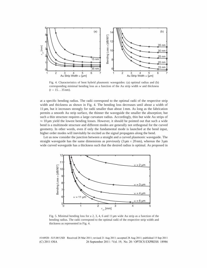
Waveguide bends are essential for the design of integrated plasmonic circuits. As previouslyinvestigated by Berini et al., an optimal radius ropt for a given plasmonic waveguide exists,where the radiation and absorption losses are minimized [22]. Recently, it was shown thathybrid plasmonic waveguides embedded in a dielectric layer allow to reduce ropt further [15].This is illustrated in Fig. 4, which gives the optimal radii and the corresponding bending lossesas a function of the plasmonic waveguide geometry. Note that the minimum optimal radius isbarely less than half a millimeter for a 35nm thick waveguide. For a given thickness, the optimalradius and the minimal bending losses can be reduced by increasing the metal strip width, up toabout 11µm. Figure 5 indicates the minimal bending losses for a waveguide width of 2. . . 11µm
#144920 - $15.00 USD Received 28 Mar 2011; revised 21 Aug 2011; accepted 28 Aug 2011; published 15 Sep 2011(C) 2011 OSA 26 September 2011 / Vol. 19, No. 20 / OPTICS EXPRESS 18985
1 2 3 4 5 6 70
1
2
3
4
5
6
15 nm
35 nm
Au Strip Width w [μm]
r opt
[mm
]
(a)
1 2 3 4 5 6 76
8
10
12
14
15 nm
20 nm
25 nm
30 nm
35 nm
Au Strip Width w [μm]
Ben
ding
Los
s α
[dB
/90°
]
(b)
Fig. 4. Characteristics of bent hybrid plasmonic waveguides: (a) optimal radius and (b)corresponding minimal bending loss as a function of the Au strip width w and thickness(t = 15. . . 35nm).
at a specific bending radius. The radii correspond to the optimal radii of the respective stripwidth and thickness as shown in Fig. 4. The bending loss decreases until about a width of11µm, but it increases strongly for radii smaller than about 1mm. As long as the fabricationpermits a smooth Au strip surface, the thinner the waveguide the smaller the absorption; butsuch a thin structure requires a large curvature radius. Accordingly, thin but wide Au strips of≈ 10µm yield the lowest bending losses. However, it should be pointed out that such a widebend is a multimode structure and different modes are generally not orthogonal for the curvedgeometry. In other words, even if only the fundamental mode is launched at the bend input,higher order modes will inevitably be excited as the signal propagates along the bend.
Let us now consider the junction between a straight and a curved plasmonic waveguide. Thestraight waveguide has the same dimensions as previously (3µm× 20nm), whereas the 3µmwide curved waveguide has a thickness such that the desired radius is optimal. As proposed in
0 1 2 3 4 55
6
7
8
9
10
11
12
w = 2 μm
w = 3 μm
w = 4 μm
w = 6 μmw = 11 μm
ropt [mm]
Ben
ding
Los
s α
[dB
/90°
]
Fig. 5. Minimal bending loss for a 2, 3, 4, 6 and 11µm wide Au strip as a function of thebending radius. The radii correspond to the optimal radii of the respective strip width andthickness as represented in Fig. 4.
#144920 - $15.00 USD Received 28 Mar 2011; revised 21 Aug 2011; accepted 28 Aug 2011; published 15 Sep 2011(C) 2011 OSA 26 September 2011 / Vol. 19, No. 20 / OPTICS EXPRESS 18986
x
-1 0 1 2 30.70
0.75
0.80
0.85
0.90
0.95
1.00
Lateral Offset x [μm]
Cou
plin
g E
ffici
ency
C
xopt
(a)
-100 -50 0 50 1000.930
0.935
0.940
0.945
0.950
0.955
0.960
Vertical Offset y [nm]
(b)
y
xopt
Cou
plin
g E
ffici
ency
C
Fig. 6. Lateral and vertical offset between a straight and bent hybrid waveguide: Couplingefficiency as a function (a) of the lateral offset and (b) of the vertical offset. The Au stripsof the straight and bent waveguide are 3µm×20nm and 3µm×10nm, respectively.
[22] and applied for dielectric waveguides, the coupling efficiency can be improved by laterallyoffseting the curved waveguide towards the center. Figure 6(a) shows the coupling efficiencyas a function of the lateral offset. Here, the coupling between a 20nm thick straight waveguideand a 10nm thick bend with a radius r0 = ropt = 8mm is considered. We acknowledge that evenif this configuration is favorable in terms of coupling losses, it would be technically difficultto fabricate because the metal thickness varies between the straight and the bend waveguide.In addition, achieving a smooth 10nm thick bend using standard metal deposition techniquesappears challenging because evaporated metallic films are typically not smooth for thicknessessmaller than 20nm or so [47]. Since the straight and the curved waveguide do not have thesame thickness in this case, the coupling efficiency as a function of a vertical offset must alsobe investigated. This is shown in Fig. 6(b), where the vertical offset is measured from the centerposition at an optimal lateral shift. As long as one waveguide section lies within the other, anoptimal coupling is observed. Thus, there is no significant reduction of the coupling efficiencywhen the bottom of both guides are aligned at the same height, which considerably simplifies
1 2 3 4 510
15
20
25
30
35
Au
Thic
knes
s t [
nm]
1 2 3 4 50.20
0.25
0.30
0.35
0.45
Optimal Radius r0 [mm]
Cou
plin
g Lo
ss αC [d
B]
0 1 2 3 4 50.25
0.30
0.35
0.40
0.45
0.50
0.55
Optimal Radius r0 [mm]
x
Opt
imal
Lat
eral
Offs
et x
[μm
]
0.40
(b)(a)
Fig. 7. Straight and optimally bent waveguide coupling: (a) Au strip thickness and couplingloss as a function of the optimal radius. (b) Optimal lateral offset as a function of the optimalradius. The Au strip is 3µm wide.
#144920 - $15.00 USD Received 28 Mar 2011; revised 21 Aug 2011; accepted 28 Aug 2011; published 15 Sep 2011(C) 2011 OSA 26 September 2011 / Vol. 19, No. 20 / OPTICS EXPRESS 18987
the fabrication process.With all optimization elements at hand, the minimal coupling loss as a function of the bend-
ing radius can now be calculated for a portion of the circuit shown in Fig. 1. Both, the straightand the curved waveguides are 3µm wide. The thickness is 20nm for the straight waveguide.The thickness of the curved one is such that the bending radius is optimal. For a thick Au strip,the corresponding optimal radius is small. This dependency can be seen in the solid line inFig. 7(a) (in this figure, the origin of the small bump in the coupling loss curve around 3µm isnot clear and does not appear to be caused by the mesh used for the calculation). The dashedline in this figure corresponds to the coupling losses. The coupling losses reach their minimumwhen the curved waveguide has about the same thickness as the straight one since the fielddistributions are similar in that case. However, it should be noted that the coupling losses areabout ten times smaller than the bending losses (see Fig. 5). Figure 7(b) shows the lateral offsetfor minimal coupling losses as a function of the bending radii. The larger the radius, the smallerthe required offset.
4. Conclusion
We presented a flexible and convenient approach for the simulation of complete plasmoniccircuits realized with different waveguide elements such as straight and bent waveguides. Theimplementation using a commercial finite element solver of different waveguide geometries —including bends — has been detailed, together with the required specific boundary conditions.This method was successfully applied to design integrated plasmonic circuits. Waveguide cou-pling and curvature have been optimized for minimal losses. Provided a low reflexion coupling,the losses due to the coupling are about 10 times lower than those caused by ninety degreebends. Therefore bending losses remain the most critical issue for the integration of long–rangeplasmonic waveguides.
Acknowledgments
Funding from the Swiss National Center of Competence in Research Nanoscale Science isgratefully acknowledged.
#144920 - $15.00 USD Received 28 Mar 2011; revised 21 Aug 2011; accepted 28 Aug 2011; published 15 Sep 2011(C) 2011 OSA 26 September 2011 / Vol. 19, No. 20 / OPTICS EXPRESS 18988


![2892 IEEE TRANSACTIONS ON ANTENNAS AND … › ~amhwong › papers › (AMHW 2018...superscatterer [20] implemented through the transformation optics approach, and a plasmonic superscatterer](https://static.documents.pub/doc/80x56/60b74c55fb43e832283c8dbb/2892-ieee-transactions-on-antennas-and-a-amhwong-a-papers-a-amhw-2018.jpg)


