+ All Categories
Home > Documents > SIMULATION OF SINGLE ELECTRON TRANSISTOR...

SIMULATION OF SINGLE ELECTRON TRANSISTOR...

Date post: 07-Apr-2019
Category:
Upload: vandiep
View: 221 times
Download: 0 times
Share this document with a friend
28
SIMULATION OF SINGLE ELECTRON TRANSISTOR (SET) CIRCUITS USING MONTE CARLO METHOD SYABANI BIN AHMAD A project report submitted in partial fulfillment of the requirements for the award of the degree of Masters of Engineering (Electrical – Electronics & Telecommunication) Faculty of Electrical Engineering Universiti Teknologi Malaysia JUNE 2007
Transcript

SIMULATION OF SINGLE ELECTRON TRANSISTOR (SET)

CIRCUITS USING MONTE CARLO METHOD

SYABANI BIN AHMAD

A project report submitted in partial fulfillment of the

requirements for the award of the degree of

Masters of Engineering (Electrical – Electronics & Telecommunication)

Faculty of Electrical Engineering

Universiti Teknologi Malaysia

JUNE 2007

iii

ACKNOWLEDGEMENTS

I would like to express my gratitude and appreciation to my supervisor,

Assosiate Prof. Dr Razali bin Ismail, for his guidance in the execution of the project,

for keeping me on my toes, and for his kind understanding. I am especially grateful

for all the help he provided and resources he made available without which the

project would not have reached its current stage. I would also like to thank Dr

Zaharuddin bin Mohamed, for being most efficient in coordinating the project. My

acknowledgement also goes out to the project presentation assessors, PM. Dr. Abu

Khari bin A’ain and Dr. Abdul Manaf bin Hashim who have given me much advice

and guidance during the project presentation. Last but not least, I would like to thank

my family for just being there, giving me the strength and much needed moral

support.

iv

ABSTRACT

The very fast switching characteristics and very low power consumption have given

the single electron transistor (SET) promising capabilities to replace CMOS

transistors in some semiconductor applications. SET theory of operation is now well

established nevertheless the transistor is still under laboratory investigations in the

fields of fabrication and applications in Large Scale Integration (LSI). Simulation of

SET consumes a great deal of computer time, which arises a need to renovate fast

and accurate simulation algorithms. This paper presents a simple model for SET

circuits, based on the orthodox theory, which calculates carrier transfer rates from

source to drain of the transistor by utilizing statistical mechanics. The simulator that

is used for this project is MOSES version 1.2 (Monte Carlo Single Electron

Transistor Simulator) which has been developed by Ruby Chen in Year 1997. The

reason for choosing this program is because it is free and sufficient to simulate SET

circuits such as Array, Junction and SET.

v

ABSTRAK

Ciri pensuisan pantas dan penggunaan kuasa yang rendah menjadikan SET sebagai

pesaing utama bagi CMOS di dalam industri semikonduktor. Walaupun teknologi

ini masih di peringkat kajian makmal bagi menyelesaikan isu fabrikasi dan Integrasi

Skala Besar (LSI), namun teori tentang bagaimana SET beroperasi telah diterima

ramai. Simulasi SET melibatkan masa pemprosesan komputer yang lama, oleh itu

algoritma yang efficient harus diguna pakai. Kertas projek ini membentangkan

model litar SET yang ringkas berdasarkan teori ortodoks yang mengira kadar

pemindahan pembawa dari sumber ke pemungut menggunakan statistik mekanik.

Simulator yang digunakan adalah Monte Carlo Single Electron Transistor (MOSES

versi 1.2) yang telah dibangunkan oleh Ruby Chen pada tahun 1997. Ianya telah

dipilih berdasarkan lesennya yang percuma dan berkesan didalam proses simulasi

litar SET seperti Array, Junction dan SET.

vi

TABLE OF CONTENT

CHAPTER TITLE PAGE

DECLARATION ii

ACKNOWLEDGEMENTS iii

ABSTRACT iv

ABSTRAK v

TABLE OF CONTENTS vi

LIST OF TABLES x

LIST OF FIGURES xi

LIST OF APPENDICES xiv

1 INTRODUCTION 1

1.1 Problems Faced to Scale-down MOSFET 3

1.2 Potential Nanoelectronics Devices and Application Areas 5

1.2.1 Single electron memory [6] 5

1.2.2 High sensitivity electrometer [6] 6

1.2.3 Microwave detection [6] 7

1.2.4 Application in the Metrology Area [7] 7

1.3 Theory of SET 8

1.4 History of SET 11

1.5 Types of SETS [8] 13

1.6 Objectives of the project 15

1.7 Scope of the project 16

1.8 Motivations 16

1.9 Methodology and Report Structure 16

vii

2 MONTE-CARLO SINGLE-ELECTRONS TRANSITOR

SIMULATOR 11

2.1 Simulation Approaches of Single Electron Circuits 20

2.1.1 SPICE macro-modeling 20

2.1.2 Monte Carlo [7] 20

2.1.3 Master Equation [7] 21

2.1.4 Advantages/ Disadvantages of Monte Carlo method 23

2.2 Simulators 24

2.2.1 MOSES Simulator 25

2.2.2 SIMON Simulator 26

2.2.3 KOSEC Simulator 28

2.2.4 SENECA Simulator 28

2.2.5 SPICE Simulator 28

2.3 Models of SETs 29

2.3.1 SET Model [37] 29

2.3.2 Single Electron Tunnel Junction 31

2.3.3 Coulomb blockade Model [38] 31

2.4 Conclusion 32

3 METHODOLOGY 29

3.1 Introduction of SET circuit modeling using MOSES [40] 33

3.2 Minimum Hardware and Software requirement [40] 34

3.3 Installation of MOSES [40] 34

3.4 Modeling SET circuit with MOSES [40] 35

4 RESULTS AND DISCUSSION

4.1 Problem of Making More Powerful Chips [38] 45

4.2 SET Transistor Function [38] 46

4.3 What is the “island”? 47

4.4 Coulomb blockade [39] 49

4.5 Single electron transistor with niobium leads and aluminum

island 51

4.6 Junction circuit simulation results 52

4.6.1 IV curve of Junction circuit 53

viii

4.6.5 Spectral Densities of Island Potentials 60

4.7 SET circuit simulation result 61

4.7.1 IV curve of SET circuit 62

4.7.4 Spectral Densities of Island Potential 67

4.8 Array circuit simulation result 68

4.8.1 IV curve of Array circuit 70

4.8.5 Spectral Densities of Island Potentials 75

4.8.6 Energy of a 21-junction array 76

4.8.7 Energies of a 21-junction array with different Vds

values 77

4.9 Comparison of Spectral Densities between Junction, SET and

Array circuit. 78

5 CONCLUSIONS AND FURTHER WORK

5.1 Positive Conclusion 79

5.2 Further improvement for this Project 79

5.3 Future research 79

5.4 A Final Note 80

REFERENCES 81

Appendix A 85 - 120

ix

LIST OF FIGURES

FIGURE NO. TITLE PAGE

1.1 Transfer of electrons 18

1.2 Tunnel Junction 10

1.3 SET is type of switching device 10

1.4 Energy level diagram 11

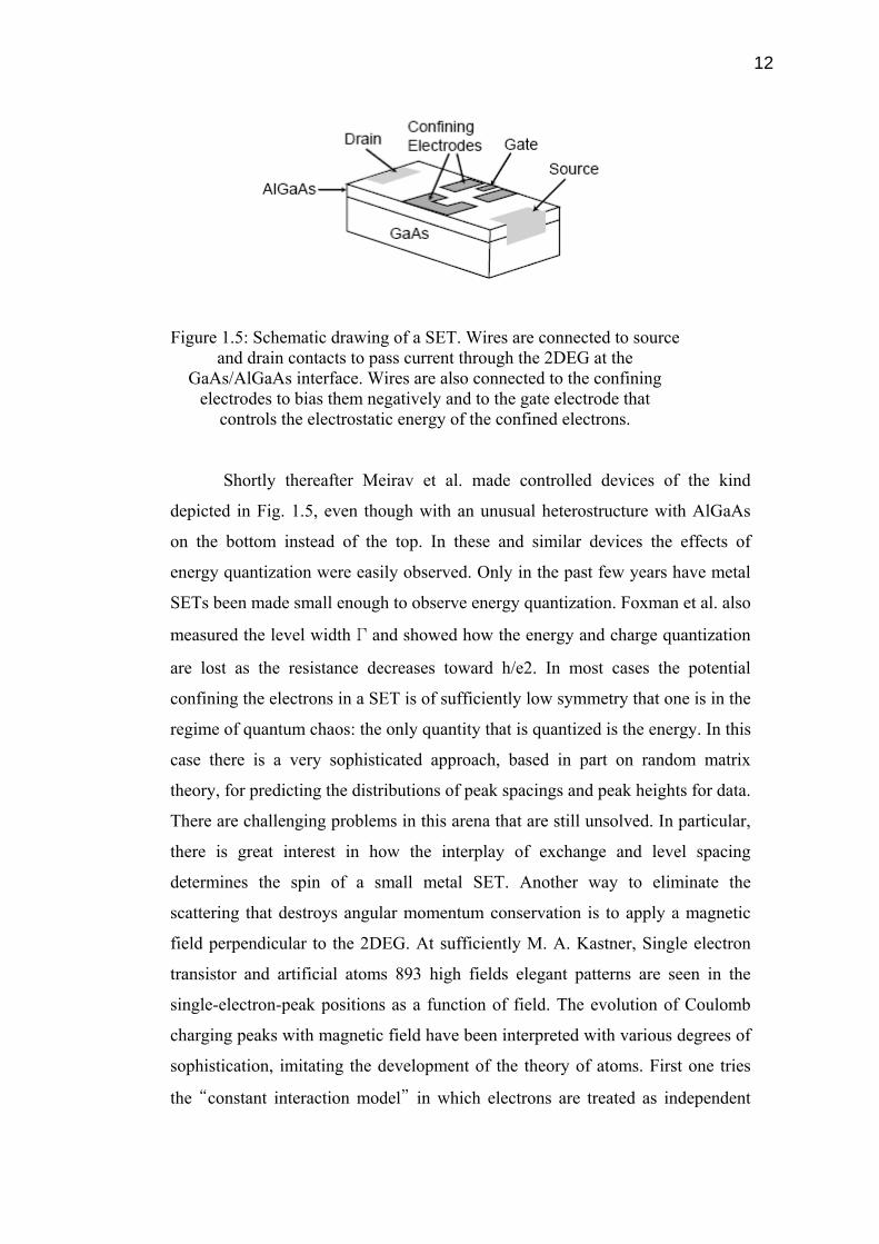
1.5 Schematic drawing of a SET 12

1.6 Flowchart on Project Methodology 16

1.7 Linux on VMWare 17

1.8 MOSES in Linux environment 18

2.1 Screenshot of MOSES 26

2.2 Screenshot of SIMON graphical interfaces 27

3.1 Tunnel junction circuit 36

4.1 A single-electron transistor diagram 46

4.2 Tunnel junction capacitance 47

4.3 Characteristic for two different gate voltages 48

4.4 IV curve of Single electron transistor 49

4.5 Tunnel Junction circuit 52

4.6 IV curve of Junction circuit with default value 53

4.7 IV curve with different Temperature value 54

4.8 IV curve with different Capacitance value 55

4.9 IV curve of Junction circuit with different capacitance value 56

4.10 IV curve of Junction circuit with different Resistance value 57

4.11 IV curve of Junction circuit with different Resistance value 58

4.12 IV curve of Junction circuit with different Resistance value 59

4.13 Spectral Densities of Island Potentials for Junction circuit 60

4.14 SET circuit 61

4.15 IV curve of SET circuit with default value 62

x

4.16 IV curve of SET circuit with different set of Temperatures 63

4.17 IV curve of SET with different set of capacitance (C2 variable) 64

4.18 IV curve of SET with different set of capacitance (C1 variable) 65

4.19 IV curve of SET with different set of capacitance (C2=C1) 66

4.20 Spectral Densities of Island Potential for SET circuit 67

4.21 Array circuit diagram 68

4.22 IV curve of Array circuit with default value 70

4.23 IV curve of Array circuit with different Temperature value 71

4.24 IV curve of Array circuit with variable Capacitance 72

4.25 IV curve of Array with variable Capacitance (increment and

decrement order) 73

4.26 IV curve of Array circuit with different conductance value 74

4.27 Spectral Densities of Island Potentials for Array circuit 75

4.28 Energy of 21-junction array circuit 76

4.29 Energies of a 21-junction array with one extra electron on node i 77

4.30 Comparison of Spectral Densities of Island potentials for Junction,

SET and Array circuit. 78

xi

LIST OF APPENDIX

APPENDIX TITLE PAGE

A Monte-Carlo Single Electronics Simulator 85

CHAPTER 1

INTRODUCTION This project studies about the single electron transistor (SET) properties by

simulating 3 types of circuits with Monte-Carlo Single Electronics Simulator

(MOSES). Single-electron transistor (SET) is a device to amplify current in

nanoelectronics. Basically there are three types of SET circuit based on its scale. The

first one is tunnel junction which in short is called Junction, is the elementary

structure of SET. The second one is the SET itself which consists of 2 tunnel

junction. The third one consists of more than one SET (in this project is 21) and is

called Array circuit. As explained in Result and Discussion, we can see a

tremendous different among this three for IV curve, Spectrum densities and Energy.

We also simulate these circuits using different value of external factors such as

capacitance and temperatures.

Semiconductor electronics have seen a sustained exponential decrease in size

and cost and a similar increase in performance and level of integration over the last

thirty years. From computers that take up the entire room to handhelds to embedded

computers. George E. Moore, the co-founder of Intel had predicted this in what is

known as the Moore’s Law.

“The complexity for minimum component costs has increased at a

rate of roughly a factor of two per year ... Certainly over the short

term this rate can be expected to continue, if not to increase. Over

the longer term, the rate of increase is a bit more uncertain,

although there is no reason to believe it will not remain nearly

constant for at least 10 years. That means by 1975, the number of

2

components per integrated circuit for minimum cost will be 65,000.

I believe that such a large circuit can be built on a single wafer.”

Although Moore's Law was initially made in the form of an observation and

forecast, the more widely it became accepted, the more it served as a goal for an

entire industry. This drove both marketing and engineering departments of

semiconductor manufacturers to focus enormous energy aiming for the specified

increase in processing power that it was presumed one or more of their competitors

would soon actually attain. In this regard, it can be viewed as a self-fulfilling

prophecy. And Moore’s Law is expected to hold for at least the next decade.

Based on Moore’s Law, a consortium of integrated circuit manufacturers

called the Semiconductor Industry Association (SIA) produced and estimate of how

technology is expected to evolve. The following table shows a sample of the SIA

roadmap [1].

Year 1999 2001 2004 2006 2009 2012

Transistor

gate length

0.14 µm 0.12 µm 90 nm 65 nm 50 nm 35 nm

Transistors

per cm2

14 million 16 million 24 million 40 million 64 million 100 million

Chip size 80 mm2 850 mm2 900 mm2 1000 mm2 1100 mm2 1300 mm2

Table 1: A sample of the SIA Roadmap

The first row of the table indicates that the minimum gate length is

expected to reduce steadily to about 35nm by year 2012. The size of transistors

determines how many transistors can be placed in a given amount of chip area.

We can see the need for smaller transistors, hence the driving force behind the

research of SETs.

SETs have been widely studied and demonstrated due to the maturity and

variety of their process technologies. These devices based on the single-electron

charging effect, i.e., the Coulomb blockade in Si nanostructures, are promising

3

because their operation principle becomes more robust as the device size is scaled

down unlike MOSFET, which will be further explained in the following section.

Moreover, their power consumption is quite low. However, SETs are not expected to

replace the conventional CMOS logic devices because of their inherent limitations

such as a low voltage gain and current drivability. In contrast, new functionalities of

SETs, such as quantum cellular automata (QCA), binary decision diagram (BDD)

devices, and the multivalued logic, have been explored extensively [2].

1.1 Problems Faced to Scale-down MOSFET

The metal-oxide-semiconductor field-effect transistor (MOSFET, MOS-FET,

or MOS FET), is by far the most common field-effect transistor in both digital and

analog circuits. The MOSFET is composed of a channel of n-type or p-type

semiconductor material, and is accordingly called an NMOSFET or a PMOSFET

(also commonly called nMOSFET, pMOSFET, NMOS FET, PMOS FET, nMOS

FET, pMOS FET).

The MOSFET has become the basic element of all silicon integrated circuits.

The growth of digital technologies like the microprocessor has provided the

motivation to advance MOSFET technology faster than any other type of silicon-

based transistor. The principal reason for the success of the MOSFET was the

development of digital CMOS logic, which uses p- and n-channel MOSFETs as

building blocks. The great advantage of CMOS logic is that they allow no current to

flow (ideally), and thus no power to be consumed, except when the inputs to logic

gates are being switched. CMOS accomplishes this by complementing every

nMOSFET with a pMOSFET and connecting both gates and both drains together. A

high voltage on the gates will cause the nMOSFET to conduct and the pMOSFET

not to conduct and a low voltage on the gates causes the reverse. During the

switching time the voltage goes from one state to another and both will conduct.

This arrangement greatly reduces power consumption and heat generation.

4

Overheating is a major concern in integrated circuits, since ever more transistors are

packed into ever smaller chips.

The steady reduction in the minimum feature size in integrated circuits has

helped the microelectronic industry to produce products with spectacular increase in

computational capability and integration density at lower cost. Smaller transistors

operate faster than larger ones, and for a given chip technology, the cost of a chip

decreases with area rather than with the number of transistors. As scaling down of

MOSFET proceeds, we are faced with extremely shallow source and drain (S/D)

junctions with low resistances.

As for the CMOS, when its dimension is scaled to the deep nanometer arena,

in particular the channel length, the electrical barriers in the device begin to lose

their insulating properties due to thermal injection and quantum-mechanical

tunneling. This results in a rapid rise of the standby power of the chip, placing a

limit on the integration level as well as on the switching speed.

The major limiting factors are power and threshold voltage, tunneling

leakage through gate oxide, lithography, short-channel effect, high-field effects,

dopant number fluctuations, interconnect delays and electrostatic scale length. Both

the standby power and the active power of a chip will increase precipitously below

the 45nm technology generation.

Conventional scaling will no longer be sufficient to continue device

performance by creating smaller MOSFET/CMOS, it will be running into

fundamental barriers of physics. It is reported in [3] that the minimum MOSFET

structure for a power supply voltage of 1.5V has a channel length of 0.52µm and a

gate oxide thickness of 9.4 nm. Difficult challenges lie ahead in tightening process

tolerances to satisfy more stringent defect density and reliability requirements in

future generation CMOS technologies. Thus, alternatives like SETs are being

pursued.

5

1.2 Potential Nanoelectronics Devices and Application Areas

Single-electron tunneling (SET) devices have been proposed in [4] as one

promising candidate for future nanoelectronic integrated circuits. SETs have

appealing properties for implementing ultra-dense and complex signal and image

processing systems. The potential for very dense arrays of SET transistors makes

them attractive for the realization of cellular non-linear network (CNN)

circuits, where locally-connected cells may alleviate the interconnect problem

facing conventional architectures as they scale. In this paper, the use of

nanoelectronic structures in CMOS-type digital circuits and in analog CNN

architectures for potential application in future high-density and low-power

CMOS-nanodevice hybrid circuits are investigated. The simple SET-CNN cell

acts as a summing node that is capacitively coupled to the inputs and outputs of

nearest neighbour cells.

SETs are also of increasing interest for their potential in room

temperature application, high density memory and logic circuits with

conventional silicon VLSI processing techniques because of its small size, low

power consumption and high sensitivity.

It is reported in [7] that memory device is the most promising and lucrative

application of SETs, which in principle could store one bit of information with one

electron. Several companies have single-electron memory products in their roadmap

for a planned release in the 2010 to 2015 time frame.

1.2.1 Single electron memory [6]

Scientists have long been endeavored to enhance the capacity of memory

devices. If single electron memory can be realized, the memory capacity is possible

to reach its utmost limit. SET can be used as memory cell since the state of Coulomb

6

island can be changed by the existence of one electron. Chou and Chan first pointed

out the possibility of using SET as memories in which information is stored as the

presence or absence of a single electron on the cluster. They fabricated a SET by

embedding one or several nano Si powder in a thin insulating layer of SiO2, then

arranging the source and drain as well as gate around this Coulomb island. The

read/write time of Chan's structure is about 20ns, lifetime is more than 109 cycles,

and retention time (during which the electron trapped in the island will not leak out)

can be several days to several weeks.

These parameters would satisfy the standards of computer industry, so SET

can be developed to be a candidate of basic computer units. If a SET stands for one

bit, then an array of 4~7 SETs will be substantial to memorize different states. The

properties of the memory unit composed of SETs are far more advantageous than

that of CMOS. But the disadvantage is the practical difficulty in fabrication. When

the time comes for the large scale integration of SETs to form logic gates, the full

advantages of single electron memory will show. This is the threshold of quantum

computing.

1.2.2 High sensitivity electrometer [6] The most advanced practical application currently for SETs is probably the

extremely precise solid-state electrometers (a device used to measure charge). The

SET electrometer is operated by capacitively coupling the external charge source to

be measured to the gate. Changes in the SET source-drain current are then measured.

Since the amplification coefficient is very big, this device can be used to measure

very small change of current.

Experiments showed that if there is a charge change of e/2 on the gate, the

current through the Coulomb island is about 109 e/sec. This sensitivity is many

orders of magnitude better than common electrometers made by MOSFET. SETs

have already been used in metrological applications as well as a tool for imaging

7

localized individual changes in semiconductors. Recent demonstration of single

photon detection and RF operation of SETs make them exciting for new applications

ranging from astronomy to quantum computer read-out circuitry.

The SET electrometer is in principle not limited to the detection of charge

sites on a surface, but can also be applicable to a wide range of sensitive chemical

signal transduction events as well. For example, the gate can be made coupling with

some molecules, thus can measure other chemical properties during the process.

However, as Lewis K M etc. pointed out , SETs electrometer must be designed with

care. If the device under test has a large capacitance, it is not advantageous to use

SETs as an electrometer. Since for a typical SET, CSET <1μF, the suppression factor

becomes unacceptable when the macroscopic device has a capacitance in the pF or

nF range.

Therefore, SET amplifiers are not currently used for measuring real

macroscopic devices. Other low-capacitance electrometers such as a recently

proposed quantum point contact electrometer also suffer from a similar capacitance

mismatch problem. But it is believed that if the capacitance mismatch can be solved

efficiently, SETs may find many new ultra low-noise analog applications.

1.2.3 Microwave detection [6]

If a SET is attacked black body radiation, the photon-aided tunneling will

affect the charge transfer of the system. Experiments show that the electric character

of the system will be changed even by a tiny amount of radiation. The sensitivity of

this equipment is about 100 times higher than the current best thermal radiation

detector.

8

1.2.4 Application in the Metrology Area [7]

For metrology purposes one can accept setups with cryogenic temperatures

allowing structures with dimensions in the tens of nanometers. Devices for precise

current and capacitance measurements achieved by essentially counting electrons

have been built successfully. These exhibit unprecedented accuracy over traditional

methods. Super sensitive electrometers and the use of tunnel junction arrays as

single-electron primary temperature sensors are very promising application. From an

economical point of view metrology applications will hardly be noticed. But their

development can provide important insight and fresh ideas for other single-electron

application areas.

1.3 Theory of SET

The need for fast switching and lower power consumption is the main

goal of semiconductor technology. Shrinkage in device dimensions raises

switching frequencies and reduces power consumption. In sub-micron

dimensions, quantum tunneling affects the MOSFET operation due to electron

transport by tunneling from source to drain. Recently a new transistor was

invented; the single electron transistor (SET) that operates on tunneling

phenomena. This transistor turns on when one electron tunnels from source to

drain. Figure 1.1 explains clearly the difference between SET and MOSFET.

Figure 1.1: Transfer of electrons is (a) one-by-one in SET (b) conventional

MOSFET where many electrons simultaneously participate to the drain current

9

The tunnel junction is the smallest unit cell of single electron transistor. It

consists of two conductors separated by a thin insulator. Figure 1.2 shows the

diagram of tunnel junction. The only way for electrons to move across the tunnel

junction is to tunnel through. Although tunneling is a probability distribution

function, electrons tunnel across the tunnel junction in a discrete manner.

Figure 1.2: Tunnel junction consists of 2 metals that are separated by a thin

insulator. Because of the separation, capacitance is formed and they are represented by capacitor value in the circuit.

Connecting two tunnel junctions together forms what is known as the

Coulomb island, as this elemet is what we call as Single Electron Transistor

(SET). This is shown by Figure 1.3.

Figure 1.3: SET is type of switching device that uses controlled electron

tunneling to amplify current

No electron can reside on the island unless its kinetic energy exceeds the

Coulomb energy of the island, Ec, which is known as the Coulomb blockade.

10

where, C is the total capacitance of the island. The island is capacitively coupled

to the gate electrode by a thick insulating layer to prevent tunneling between the

island and the gate. With zero voltage applied to the gate, the island's Coulomb

energy blocks the current from drain to source until the drain-source voltage

exceeds the threshold voltage, Vth

The gate voltage controls the charging energy of the island and

consequently it controls the Coulomb blockade. Applying an appropriate value of

gate voltage can thus eliminate the Coulomb blockade.

Figure 1.4: Energy level diagram

Single electron transistor operation can be explained by the orthodox

theory. In this theory the tunneling rate across each tunnel junction of the

transistor is calculated. The tunnel rate is derived from the Fermi golden rule

taking into consideration the change in free energy of the system. The free energy

is equivalent to the energy change caused by a tunnel event in the orthodox

theory. The Fermi golden rule states that the transition rate (tunnel rate) is highest

when the change in free energy before and after the tunnel event is minimal. The

change in free energy is the difference between the electrostatic energy of the

system and the work done by voltage sources before and after the tunnel event.

11

The change in free energy can be simply derived by the method of critical

voltage.

Utilizing the orthodox theory with statistical mechanics develops the

master equation. It computes the time dependent occupation for each state in the

system. The drain-source current of the transistor is computed using the results of

the master equation. [5]

1.4 History of SET

The effects of charge quantization were first observed in tunnel junctions

containing metal particles as early as 1968. Later, the idea that the Coulombb

blockade can be overcome with a gate electrode was proposed by a number of

authors, and Kulik and Shekhter developed the theory of Coulomb-blockade

oscillations, the periodic variation of conductance as a function of gate voltage.

Their theory was classical, including charge quantization but not energy

quantization. However, it was not until 1987 that Fulton and Dolan made the first

SET, entirely out of metals, and observed the predicted oscillations. They made a

metal particle connected to two metal leads by tunnel junctions, all on top of an

insulator with a gate electrode underneath. Since then, the capacitances of such

metal SETs have been reduced to produce very precise charge quantization. The

first semiconductor SET was fabricated accidentally in 1989 by Scott-Thomaset

in narrow Si field effect transistors. In this case the tunnel barriers were produced

by interface charges.

12

Figure 1.5: Schematic drawing of a SET. Wires are connected to source and drain contacts to pass current through the 2DEG at the

GaAs/AlGaAs interface. Wires are also connected to the confining electrodes to bias them negatively and to the gate electrode that

controls the electrostatic energy of the confined electrons.

Shortly thereafter Meirav et al. made controlled devices of the kind

depicted in Fig. 1.5, even though with an unusual heterostructure with AlGaAs

on the bottom instead of the top. In these and similar devices the effects of

energy quantization were easily observed. Only in the past few years have metal

SETs been made small enough to observe energy quantization. Foxman et al. also

measured the level width Γ and showed how the energy and charge quantization

are lost as the resistance decreases toward h/e2. In most cases the potential

confining the electrons in a SET is of sufficiently low symmetry that one is in the

regime of quantum chaos: the only quantity that is quantized is the energy. In this

case there is a very sophisticated approach, based in part on random matrix

theory, for predicting the distributions of peak spacings and peak heights for data.

There are challenging problems in this arena that are still unsolved. In particular,

there is great interest in how the interplay of exchange and level spacing

determines the spin of a small metal SET. Another way to eliminate the

scattering that destroys angular momentum conservation is to apply a magnetic

field perpendicular to the 2DEG. At sufficiently M. A. Kastner, Single electron

transistor and artificial atoms 893 high fields elegant patterns are seen in the

single-electron-peak positions as a function of field. The evolution of Coulomb

charging peaks with magnetic field have been interpreted with various degrees of

sophistication, imitating the development of the theory of atoms. First one tries

the “constant interaction model” in which electrons are treated as independent

13

except for a constant Coulomb charging energy. This gives only a qualitative

picture of the physics. In order to be quantitative, one needs to at least treat the

electron-electron interactions self-consistently (analogous to the Thomas-Fermi

model), and for some cases one needs to include exchange and correlations. In

particular, it is found that electrons in an SET undergo a series of phase

transitions at high magnetic field. One of these is well described by Hartree-Fock

theory, but others appear to require additional correlations. [5]

1.5 Types of SETS [8]

Single-electron transistors can be made using metals, semiconductors, carbon

nanotubes, or single molecules. Aluminum SET's made with Al/AlOx/Al tunnel

junctions are the SET's that have been used most often in applications. This kind of

SET is used in metrology to measure currents, capacitance, and charge. They are

used in astronomical measurements and they have been used to make primary

thermometers. However, many fundamental single-electron measurements have

been made using GaAs heterostructures. The island of this kind of SET is often

called a quantum dot. Quantum dots have been very important in contributing to our

understanding of single-electron effects because it is possible to have just one or a

few conduction electrons on a quantum dot. The quantum states that the electrons

occupy are similar to electron states in an atom and quantum dots are therefore

sometimes called artificial atoms. The energy necessary to add an electron to a

quantum dot depends not just on the electrostatic energy of Eq. 2 but also on the

quantum confinement energy and the magnetic energy associated with the spin of

the electron states. By measuring the current that flows thorough a quantum dot as a

function of the gate voltage, magnetic field, and temperature allows one understand

the quantum states of the dot in quite some detail.

The SET's described so far are all relatively large and have to be measured at

low temperature, typically below 100 mK. For higher temperature operation, the

SET's have to be made smaller. Ono et al. [9] used a technique called pattern

14

dependent oxidation (PADOX) to make small silicon SET's. These SET's had

junction capacitances of about 1 aF and a charging energy of 20 meV. The silicon

SET's have the distinction of being the smallest SET's that have been incorporated

into circuits involving more than one transistor.

Specifically, Ono et al. constructed an inverter that operated at 27 K. Postma

et al. [10] made a SET that operates at room temperature by using an AFM to buckle

a metallic carbon nanotube in two places. The tube buckles much the same way as

a drinking straw buckles when it is bent too far. Using this technique, a 25 nm

section of the nanotube between the buckles was used as the island of the SET and a

conducting substrate was used as the gate. The total capacitance achievable in this

case is also about 1 aF.

Pashkin et al. [11] used e-beam lithography to fabricate a SET with an

aluminum island that had a diameter of only 2 nm. This SET had junction

capacitances of 0.7 aF, a charging energy of 115 meV, and operated at room

temperature.

SET's have also been made by placing just a single molecule between closely

spaced electrodes. Park et al. [12] built a SET by placing a C60 molecule between

electrodes spaced 1.4 nm apart. The total capacitance of the C60 molecule in this

configuration was about 0.3 aF. Individual molecules containing a Co ion bonded

to polypyridyl ligands were also placed between electrodes only 1-2 nm apart to

fabricate a SET. [14] In similar work, Liang et al. [13] placed a single divanadium

molecule between closely spaced electrodes to make a SET. In the last two

experiments, the Kondo effect was observed as well as the Coulomb blockade. The

charging energy in the molecular devices was above 100 meV.

One of the conclusions that can be drawn from this review of SET devices is

that small SET's can be made out of a variety of materials. Single electron transistors

with a total capacitance of about 1 aF were made with aluminum, silicon, carbon

nanotubes and individual molecules. It seems unlikely that SET's with capacitances

smaller than the capacitances of the molecular devices can be made. This sets a

15

lower limit on the smallest capacitances that can be achieved at about 0.1 aF.

Achieving small capacitances such as this has been a goal of many groups working

on SET's. However, while some of the device characteristics improve as a SET is

made smaller, some of the device characteristics get worse as SET's are made

smaller. For some applications, the single molecule SET's are too small to be useful.

As SET's are made smaller, there is an increase in the operating temperature,

the operating frequency, and the device packing density. These are desirable

consequences of the shrinking of SET devices. The undesirable consequences of the

shrinking of SET's are that the electric fields increase, the current densities increase,

the operating voltage increases, the energy dissipated per switching event increases,

and the power dissipated per unit area increases, the voltage gain decreases, the

charge gain decreases, and the number of Coulomb oscillations that can be observed

decrease.

The future of research on SETs looks very bright. There are strong efforts

around the world to make the artificial atoms in SETs smaller, in order to raise

the temperature at which charge quantization can be observed. These involve

self-assembly techniques and novel lithographic and oxidation methods whereby

artificial atoms can be made nearly as small as natural ones. This is, of course,

driven by an interest in using SETs for practical applications. However, as SETs

get smaller, all of their energy scales can be larger, so it is very likely that new

phenomena will emerge. [5]

1.6 Objectives of the project

• To study nanoelectronics devices in particular SET

• To simulate Single Electron Transistor (SET) circuits using Monte Carlo

method

• To study functions of MOSES in simulating SET circuits.

16

1.7 Scope of the project

Due to the time constraint of Project 1 and 2, three SET circuits: Array,

SET and Junction circuits are simulated. The areas of the simulation are mainly

on IV curve, Spectral densities and Energies, and observations are made on the

circuit behaviour when the value of capacitance and temperature change.

1.8 Motivations

SET is of increasing interest not only from the fundamental point of view

but also for their potential room-temperature application to very high density

memory and logic circuits with conventional silicon VLSI processing techniques.

As in the case of the conventional CMOS circuit design, the modeling of devices

and the simulation of the circuit would be a key step to design the SET circuits.

In the case of the conventional circuit, the compact simulators such as MOSES

are used to simulate the characteristics of the given circuit topology.

1.9 Methodology and Report Structure

Decide on SET circuits to simulate, external factors

Simulate SET circuits on IV curve, Spectrum densities and Energy with different factors

Conclusion on findings

VMWare 5.0, Redhat Linux 8.0 and MOSES installation

Figure 1.6: Flowchart on Project Methodology

17

Prior to MOSES installation, having Linux installed in the system is

compulsory since it only runs on Linux environment. Since there is no budget to

have dedicated PC to run specifically on Linux, I have decided to turn my PC to

run two operating systems by installing VMWare. VMWare, as its name stands

for Virtual Machine allows more than one operating system to run on the same

machine. Figure 1.7 shows Linux in Windows environment using VMWare.

Figure 1.7: By using VMWare, it is possible to have more than one OS in the

same machine After installing VMWare, Linux and MOSES, it is time to decide on what

types of SET circuits to be simulated. For this purpose three SET circuits have

been finalized: Array, SET and Junction circuits. These circuits are selected since

there are varieties on IV curve, Spectrum densities and Energy results among

them.

18

Figure 1.8: MOSES in Linux environment

After the raw results are displayed, they are then transferred to Microsoft

excel for graph plotting, since this function is having problem in MOSES

application.

Finally, there is a discussion on what have the result shown based on

comparison with current SET research community, especially from IEEE Xplore

on the net.


Recommended