Page 1
1
Simultaneous OPC- and CMP-Aware Routing
Based on Accurate Closed-Form Modeling
Graduate Institute of Electronics Engineering
Department of Electrical Engineering
National Taiwan University
March 26, 2013
Shao-Yun Fang, Chung-Wei Lin, Guang-Wan Liao,
and Yao-Wen Chang
Page 2
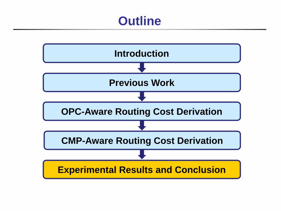
Outline
Introduction
OPC-Aware Routing Cost Derivation
CMP-Aware Routing Cost Derivation
Experimental Results and Conclusion
Previous Work
Page 3
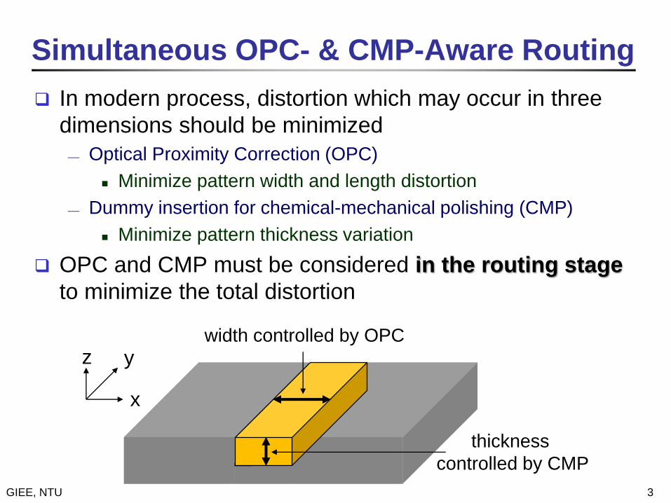
Simultaneous OPC- & CMP-Aware Routing
In modern process, distortion which may occur in three
dimensions should be minimized
Optical Proximity Correction (OPC)
Minimize pattern width and length distortion
Dummy insertion for chemical-mechanical polishing (CMP)
Minimize pattern thickness variation
OPC and CMP must be considered in the routing stage
to minimize the total distortion
3GIEE, NTU
x
yzwidth controlled by OPC
thickness
controlled by CMP
Page 4
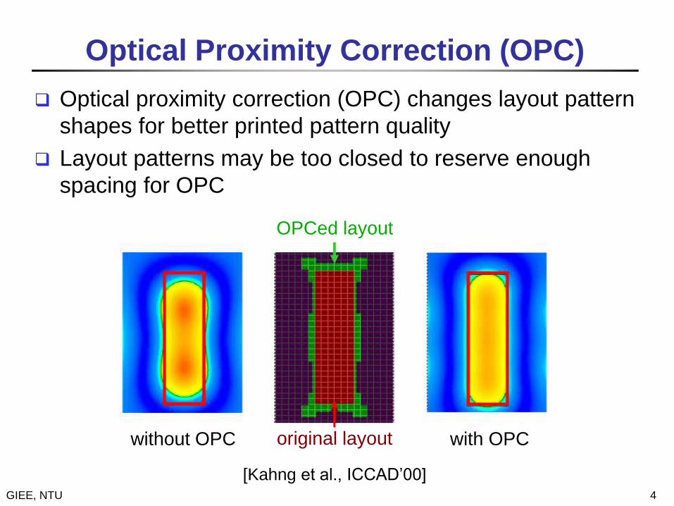
Optical Proximity Correction (OPC)
Optical proximity correction (OPC) changes layout pattern
shapes for better printed pattern quality
Layout patterns may be too closed to reserve enough
spacing for OPC
4GIEE, NTU
[Kahng et al., ICCAD’00]
OPCed layout
without OPC original layout with OPC
Page 5
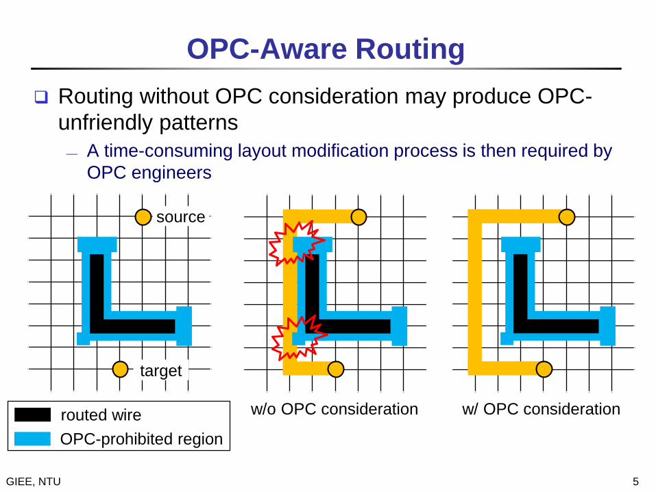
OPC-Aware Routing
5GIEE, NTU
Routing without OPC consideration may produce OPC-
unfriendly patterns
A time-consuming layout modification process is then required by
OPC engineers
w/o OPC consideration w/ OPC considerationrouted wire
OPC-prohibited region
source
target
Page 6
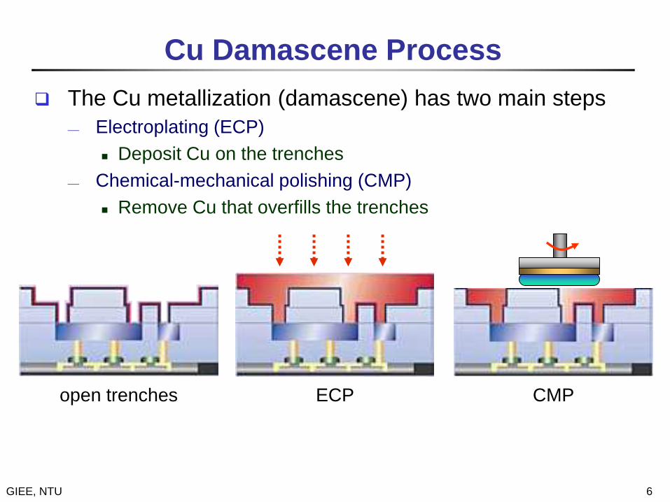
Cu Damascene Process
The Cu metallization (damascene) has two main steps
Electroplating (ECP)
Deposit Cu on the trenches
Chemical-mechanical polishing (CMP)
Remove Cu that overfills the trenches
6GIEE, NTU
ECP CMPopen trenches
Page 7
7
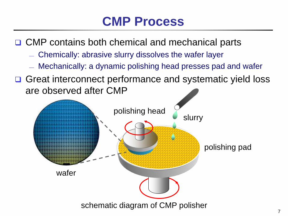
CMP Process
CMP contains both chemical and mechanical parts
Chemically: abrasive slurry dissolves the wafer layer
Mechanically: a dynamic polishing head presses pad and wafer
Great interconnect performance and systematic yield loss
are observed after CMP
schematic diagram of CMP polisher
slurry
polishing pad
polishing head
wafer
Page 8
metal dishing dielectric erosion
dielectric design feature
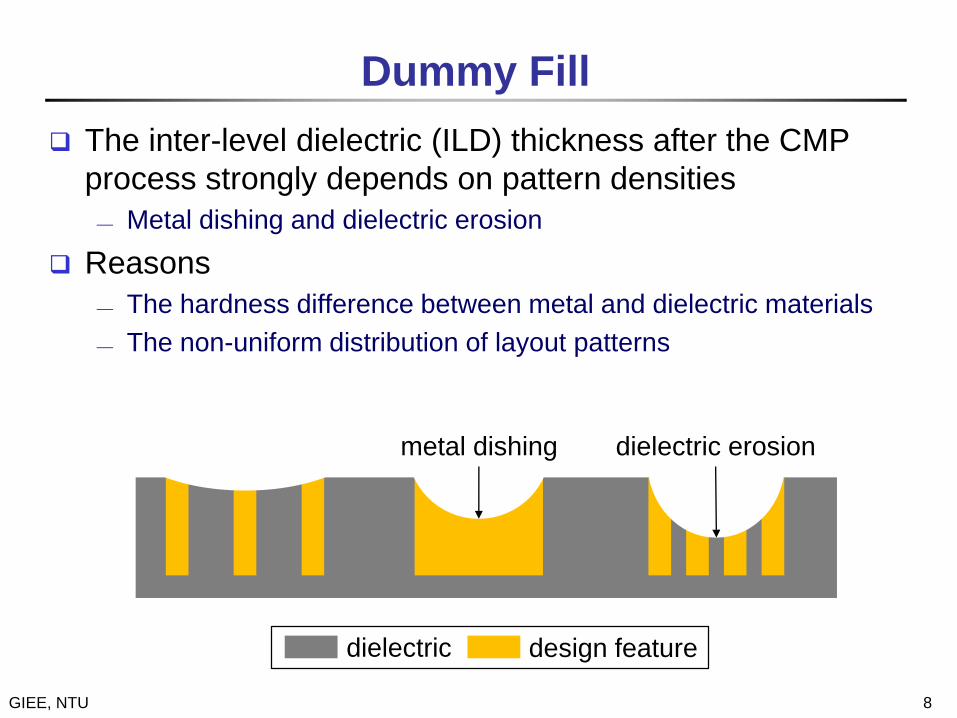
Dummy Fill
The inter-level dielectric (ILD) thickness after the CMP
process strongly depends on pattern densities
Metal dishing and dielectric erosion
Reasons
The hardness difference between metal and dielectric materials
The non-uniform distribution of layout patterns
8GIEE, NTU
Page 9
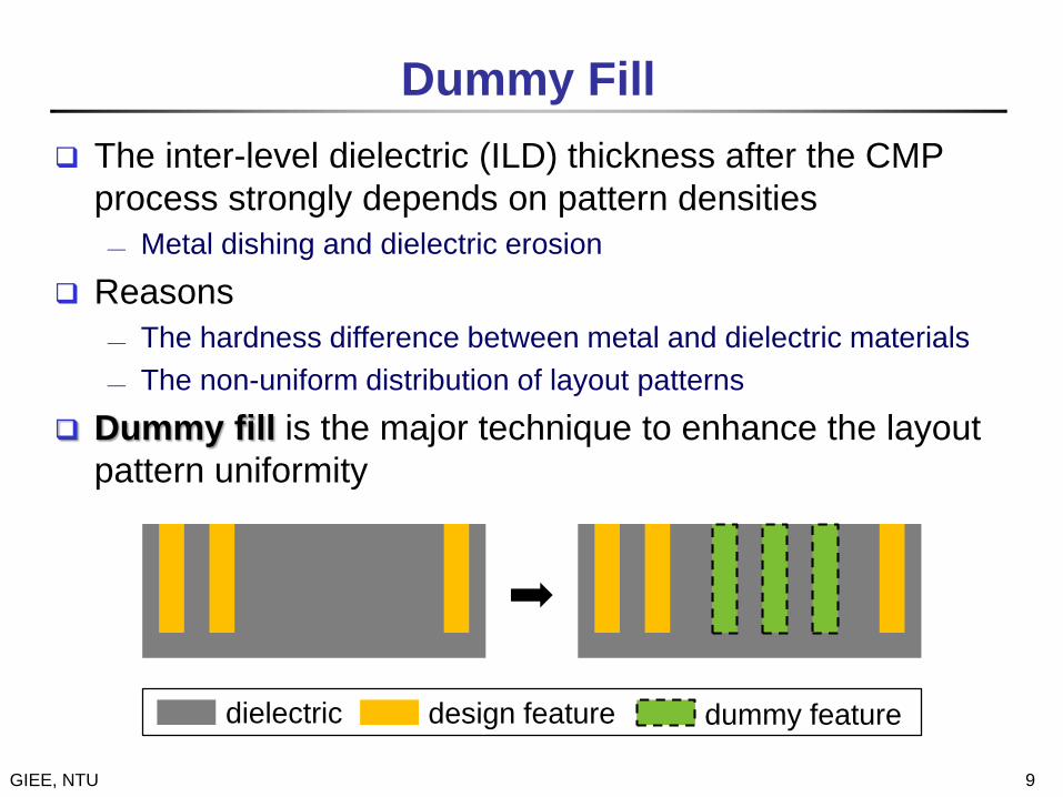
Dummy Fill
The inter-level dielectric (ILD) thickness after the CMP
process strongly depends on pattern densities
Metal dishing and dielectric erosion
Reasons
The hardness difference between metal and dielectric materials
The non-uniform distribution of layout patterns
Dummy fill is the major technique to enhance the layout
pattern uniformity
9GIEE, NTU
dielectric design feature dummy feature
Page 10
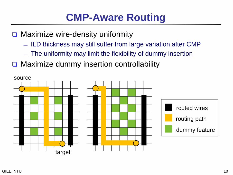
CMP-Aware Routing
Maximize wire-density uniformity
ILD thickness may still suffer from large variation after CMP
The uniformity may limit the flexibility of dummy insertion
Maximize dummy insertion controllability
10GIEE, NTU
routed wires
routing path
dummy feature
source
target
Page 11
Outline
Introduction
OPC-Aware Routing Cost Derivation
CMP-Aware Routing Cost Derivation
Experimental Results and Conclusion
Previous Work
Page 12
Previous Studies on OPC-Aware Routing
Chen et al. [TCAD’10] developed the first modeling of the
post-layout OPC
A quasi-inverse lithography technique is used to predict post-OPC
layout shapes
Off-axis illumination (OAI) is not considered
Ding et al. [DAC’11] proposed a generic lithography-
friendly detailed router
Data learning techniques are used for hotspot detection and
routing path prediction
Pattern thickness variation is not considered
12GIEE, NTU
Page 13
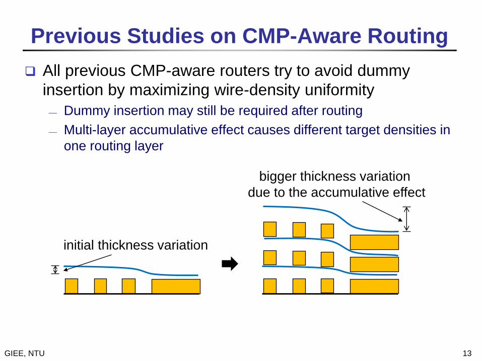
Previous Studies on CMP-Aware Routing
All previous CMP-aware routers try to avoid dummy
insertion by maximizing wire-density uniformity
Dummy insertion may still be required after routing
Multi-layer accumulative effect causes different target densities in
one routing layer
13GIEE, NTU
initial thickness variation
bigger thickness variation
due to the accumulative effect
Page 14
Outline
Introduction
OPC-Aware Routing Cost Derivation
CMP-Aware Routing Cost Derivation
Experimental Results and Conclusion
Previous Work
Page 15
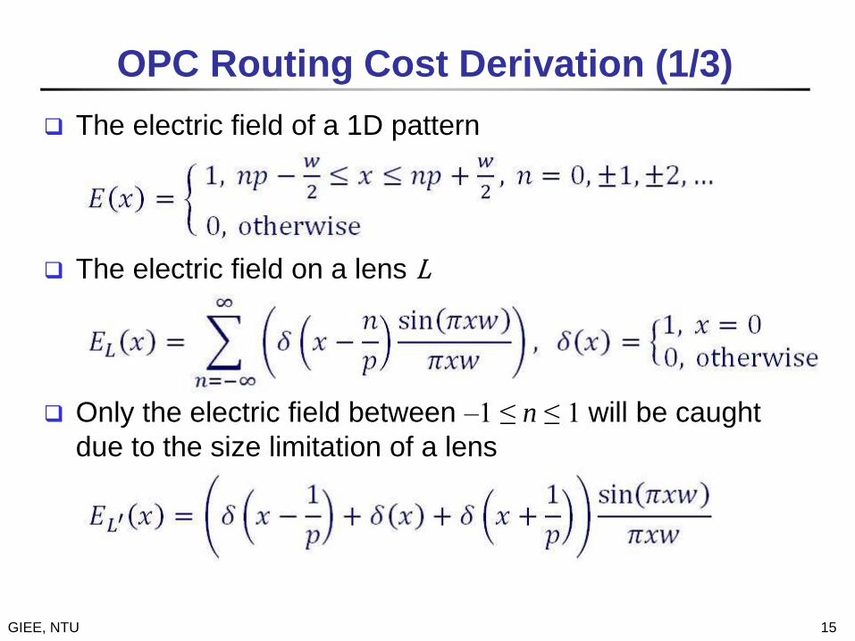
OPC Routing Cost Derivation (1/3)
The electric field of a 1D pattern
The electric field on a lens L
Only the electric field between –1 ≤ n ≤ 1 will be caught
due to the size limitation of a lens
15GIEE, NTU
Page 16
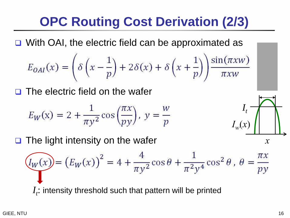
OPC Routing Cost Derivation (2/3)
With OAI, the electric field can be approximated as
The electric field on the wafer
The light intensity on the wafer
16GIEE, NTU
It: intensity threshold such that pattern will be printed
It
Iw(x)
x
Page 17
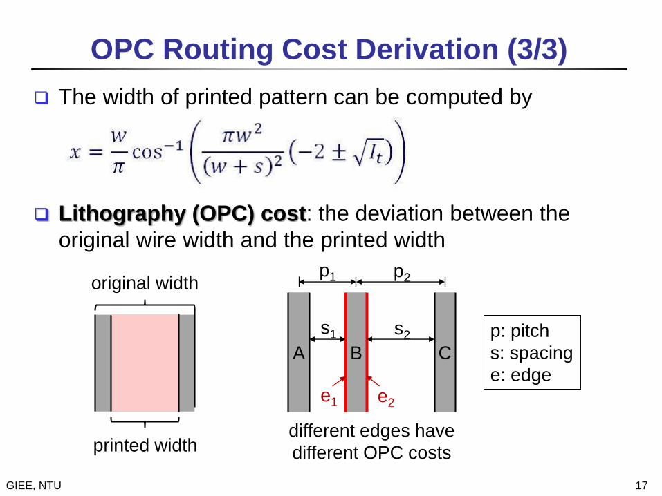
OPC Routing Cost Derivation (3/3)
The width of printed pattern can be computed by
Lithography (OPC) cost: the deviation between the
original wire width and the printed width
17GIEE, NTU
original width
printed width
A B C
p1 p2
s1 s2
e1 e2
p: pitch
s: spacing
e: edge
different edges have
different OPC costs
Page 18
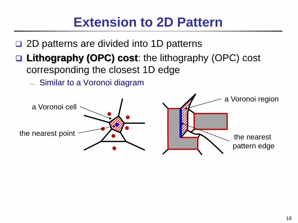
Extension to 2D Pattern
2D patterns are divided into 1D patterns
Lithography (OPC) cost: the lithography (OPC) cost
corresponding the closest 1D edge
Similar to a Voronoi diagram
18
a Voronoi cell
the nearest point
a Voronoi region
the nearest
pattern edge
Page 19
Outline
Introduction
OPC-Aware Routing Cost Derivation
CMP-Aware Routing Cost Derivation
Experimental Results and Conclusion
Previous Work
Page 20
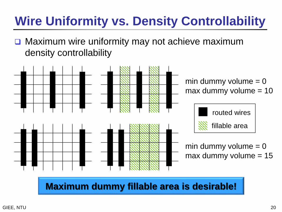
Maximum wire uniformity may not achieve maximum
density controllability
Wire Uniformity vs. Density Controllability
20GIEE, NTU
Maximum dummy fillable area is desirable!
min dummy volume = 0
max dummy volume = 15
min dummy volume = 0
max dummy volume = 10
routed wires
fillable area
Page 21
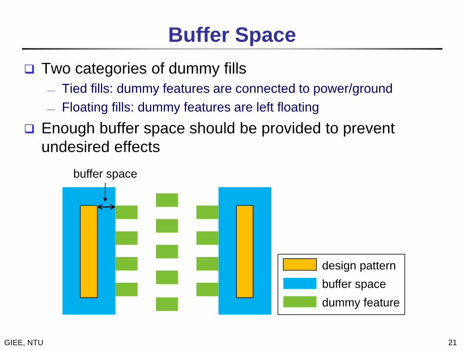
Buffer Space
Two categories of dummy fills
Tied fills: dummy features are connected to power/ground
Floating fills: dummy features are left floating
Enough buffer space should be provided to prevent
undesired effects
21GIEE, NTU
design pattern
buffer space
dummy feature
buffer space
Page 22
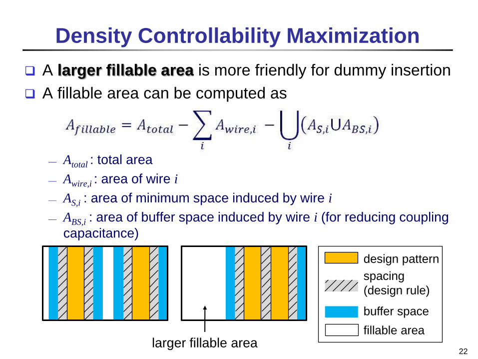
Density Controllability Maximization
A larger fillable area is more friendly for dummy insertion
A fillable area can be computed as
Atotal : total area
Awire,i : area of wire i
AS,i : area of minimum space induced by wire i
ABS,i : area of buffer space induced by wire i (for reducing coupling
capacitance)
22larger fillable area
design pattern
spacing
(design rule)
buffer space
fillable area
Page 23
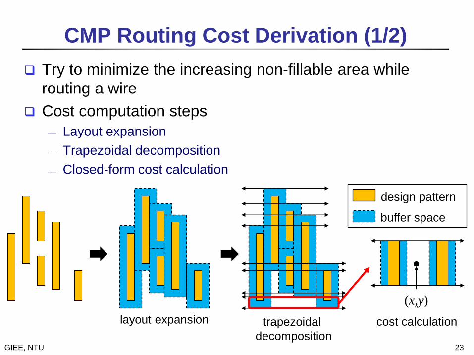
CMP Routing Cost Derivation (1/2)
Try to minimize the increasing non-fillable area while
routing a wire
Cost computation steps
Layout expansion
Trapezoidal decomposition
Closed-form cost calculation
23GIEE, NTU
design pattern
buffer space
layout expansion trapezoidal
decomposition
(x,y)
cost calculation
Page 24
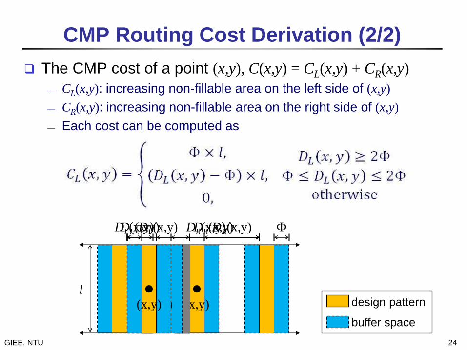
CMP Routing Cost Derivation (2/2)
The CMP cost of a point (x,y), C(x,y) = CL(x,y) + CR(x,y)
CL(x,y): increasing non-fillable area on the left side of (x,y)
CR(x,y): increasing non-fillable area on the right side of (x,y)
Each cost can be computed as
24GIEE, NTU
(x,y)
DL(x,y) DR(x,y)
design pattern
buffer space
Ф
l(x,y)(x,y)
DL(x,y) DR(x,y)DL(x,y) DR(x,y)
Page 25
Outline
Introduction
OPC-Aware Routing Cost Derivation
CMP-Aware Routing Cost Derivation
Experimental Results and Conclusion
Previous Work
Page 26
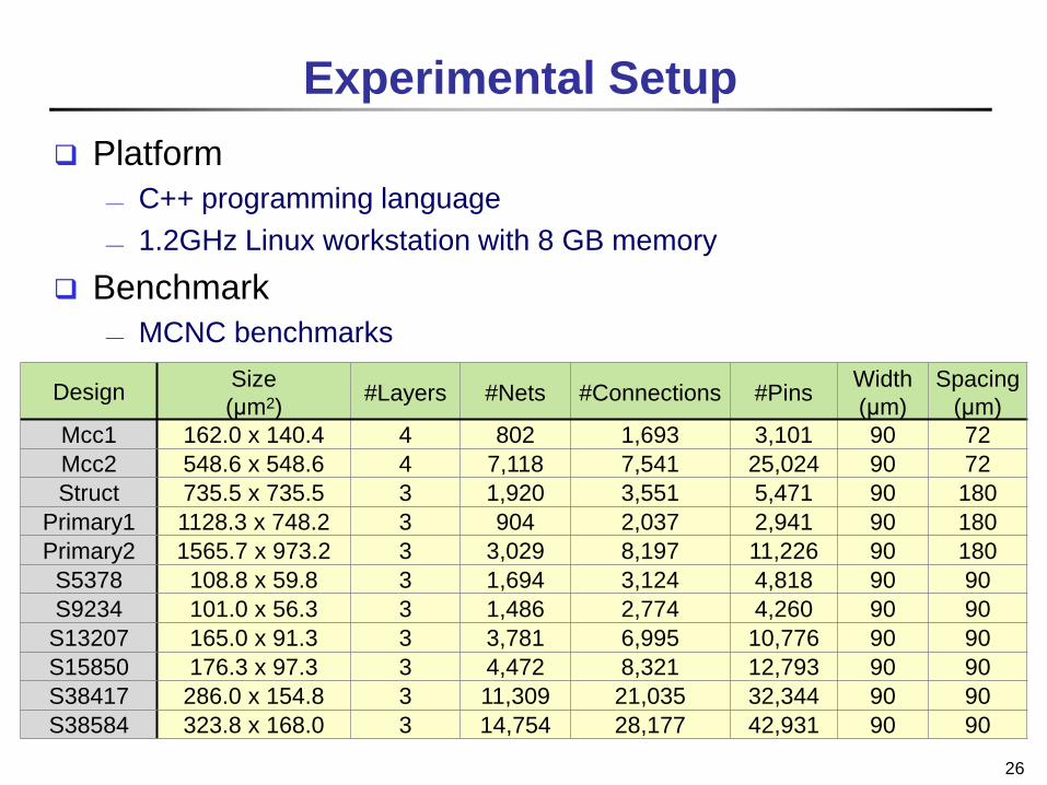
Experimental Setup
Platform
C++ programming language
1.2GHz Linux workstation with 8 GB memory
Benchmark
MCNC benchmarks
26
DesignSize
(μm2)#Layers #Nets #Connections #Pins
Width
(μm)
Spacing
(μm)
Mcc1 162.0 x 140.4 4 802 1,693 3,101 90 72
Mcc2 548.6 x 548.6 4 7,118 7,541 25,024 90 72
Struct 735.5 x 735.5 3 1,920 3,551 5,471 90 180
Primary1 1128.3 x 748.2 3 904 2,037 2,941 90 180
Primary2 1565.7 x 973.2 3 3,029 8,197 11,226 90 180
S5378 108.8 x 59.8 3 1,694 3,124 4,818 90 90
S9234 101.0 x 56.3 3 1,486 2,774 4,260 90 90
S13207 165.0 x 91.3 3 3,781 6,995 10,776 90 90
S15850 176.3 x 97.3 3 4,472 8,321 12,793 90 90
S38417 286.0 x 154.8 3 11,309 21,035 32,344 90 90
S38584 323.8 x 168.0 3 14,754 28,177 42,931 90 90
Page 27
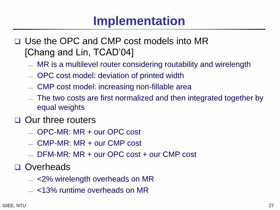
Implementation
Use the OPC and CMP cost models into MR
[Chang and Lin, TCAD’04]
MR is a multilevel router considering routability and wirelength
OPC cost model: deviation of printed width
CMP cost model: increasing non-fillable area
The two costs are first normalized and then integrated together by
equal weights
Our three routers
OPC-MR: MR + our OPC cost
CMP-MR: MR + our CMP cost
DFM-MR: MR + our OPC cost + our CMP cost
Overheads
<2% wirelength overheads on MR
<13% runtime overheads on MR
27GIEE, NTU
Page 28
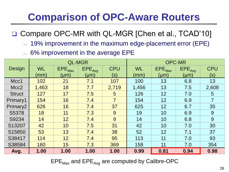
Compare OPC-MR with QL-MGR [Chen et al., TCAD’10]
19% improvement in the maximum edge-placement error (EPE)
6% improvement in the average EPE
Comparison of OPC-Aware Routers
28
Design
QL-MGR OPC-MR
WL
(mm)
EPEMax
(μm)
EPEAvg
(μm)
CPU
(s)
WL
(mm)
EPEMax
(μm)
EPEAvg
(μm)
CPU
(s)
Mcc1 102 21 7.1 107 100 13 6.8 13
Mcc2 1,463 18 7.7 2,719 1,456 13 7.5 2,608
Struct 127 17 7.5 5 126 12 7.0 5
Primary1 154 16 7.4 7 154 12 6.9 7
Primary2 626 16 7.4 37 625 12 6.7 35
S5378 18 11 7.3 9 19 10 6.9 9
S9234 14 12 7.4 9 14 10 6.8 9
S13207 42 10 7.5 31 42 10 7.0 30
S15850 53 13 7.4 38 52 12 7.1 37
S38417 114 12 7.4 95 113 11 7.0 93
S38584 160 15 7.3 369 158 11 7.0 354
Avg. 1.00 1.00 1.00 1.00 0.99 0.81 0.94 0.98
EPEMax and EPEAvg are computed by Calibre-OPC
Page 29
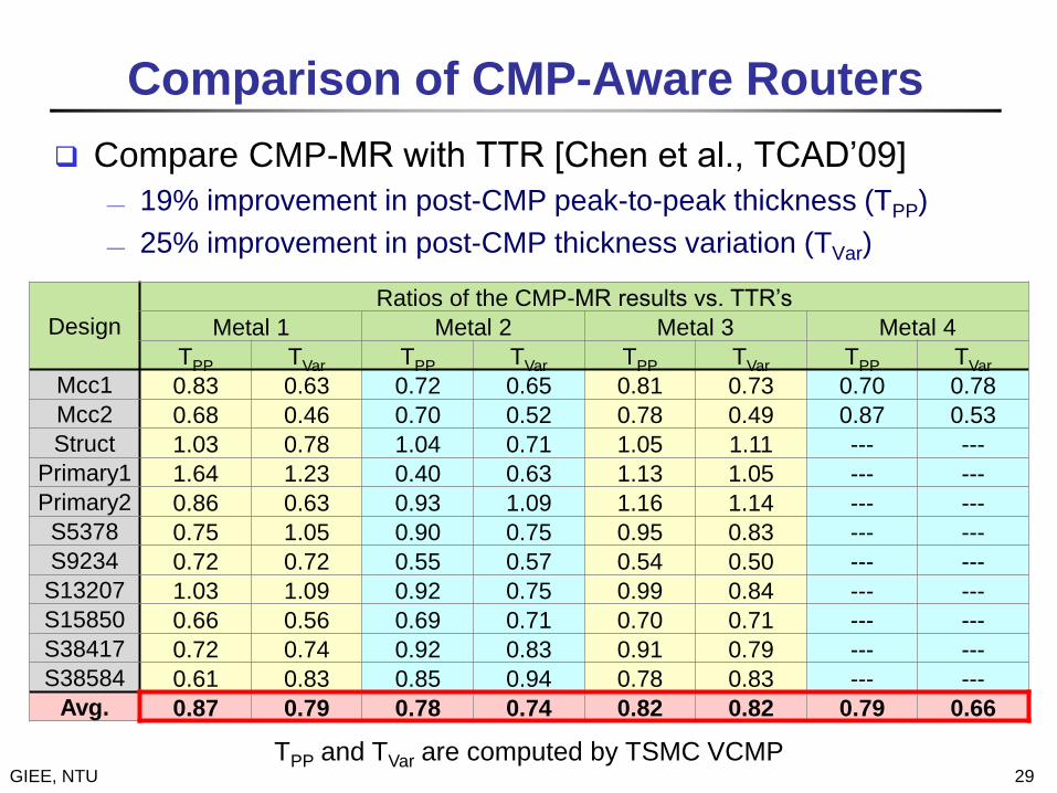
Comparison of CMP-Aware Routers
Compare CMP-MR with TTR [Chen et al., TCAD’09]
19% improvement in post-CMP peak-to-peak thickness (TPP)
25% improvement in post-CMP thickness variation (TVar)
29GIEE, NTU
Design
Ratios of the CMP-MR results vs. TTR’s
Metal 1 Metal 2 Metal 3 Metal 4
TPP TVar TPP TVar TPP TVar TPP TVar
Mcc1 0.83 0.63 0.72 0.65 0.81 0.73 0.70 0.78
Mcc2 0.68 0.46 0.70 0.52 0.78 0.49 0.87 0.53
Struct 1.03 0.78 1.04 0.71 1.05 1.11 --- ---
Primary1 1.64 1.23 0.40 0.63 1.13 1.05 --- ---
Primary2 0.86 0.63 0.93 1.09 1.16 1.14 --- ---
S5378 0.75 1.05 0.90 0.75 0.95 0.83 --- ---
S9234 0.72 0.72 0.55 0.57 0.54 0.50 --- ---
S13207 1.03 1.09 0.92 0.75 0.99 0.84 --- ---
S15850 0.66 0.56 0.69 0.71 0.70 0.71 --- ---
S38417 0.72 0.74 0.92 0.83 0.91 0.79 --- ---
S38584 0.61 0.83 0.85 0.94 0.78 0.83 --- ---
Avg. 0.87 0.79 0.78 0.74 0.82 0.82 0.79 0.66
TPP and TVar are computed by TSMC VCMP
Page 30
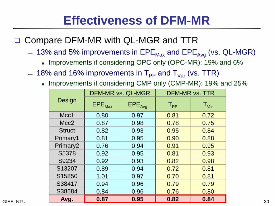
Effectiveness of DFM-MR
Compare DFM-MR with QL-MGR and TTR
13% and 5% improvements in EPEMax and EPEAvg (vs. QL-MGR)
Improvements if considering OPC only (OPC-MR): 19% and 6%
18% and 16% improvements in TPP and TVar (vs. TTR)
Improvements if considering CMP only (CMP-MR): 19% and 25%
30GIEE, NTU
DesignDFM-MR vs. QL-MGR DFM-MR vs. TTR
EPEMax EPEAvg TPP TVar
Mcc1 0.80 0.97 0.81 0.72
Mcc2 0.87 0.98 0.78 0.75
Struct 0.82 0.93 0.95 0.84
Primary1 0.81 0.95 0.90 0.88
Primary2 0.76 0.94 0.91 0.95
S5378 0.92 0.95 0.81 0.93
S9234 0.92 0.93 0.82 0.98
S13207 0.89 0.94 0.72 0.81
S15850 1.01 0.97 0.70 0.81
S38417 0.94 0.96 0.79 0.79
S38584 0.84 0.96 0.76 0.80
Avg. 0.87 0.95 0.82 0.84
Page 31
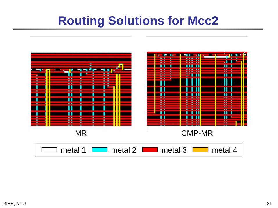
Routing Solutions for Mcc2
31GIEE, NTU
metal 1 metal 2 metal 3 metal 4
MR CMP-MR
Page 32
Conclusion
Present the first work simultaneously considering OPC
and CMP during the routing stage
Propose efficient and sufficiently accurate cost models for
OPC and CMP-aware routing
Experimental results show that the router contributes a
significant improvement for layout integrity
32GIEE, NTU