Single Channel, 128-/256-Position, I2C/SPI, Nonvolatile Digital Potentiometer
Data Sheet AD5121/AD5141
Rev. C Document Feedback Information furnished by Analog Devices is believed to be accurate and reliable. However, no responsibility is assumed by Analog Devices for its use, nor for any infringements of patents or other rights of third parties that may result from its use. Specifications subject to change without notice. No license is granted by implication or otherwise under any patent or patent rights of Analog Devices. Trademarks and registered trademarks are the property of their respective owners.
FEATURES 10 kΩ and 100 kΩ resistance options Resistor tolerance: 8% maximum Wiper current: ±6 mA Low temperature coefficient: 35 ppm/°C Wide bandwidth: 3 MHz Fast start-up time < 75 µs Linear gain setting mode Single- and dual-supply operation Independent logic supply: 1.8 V to 5.5 V Wide operating temperature: −40°C to +125°C 3 mm × 3 mm LFCSP Qualified for automotive applications
APPLICATIONS Portable electronics level adjustment LCD panel brightness and contrast controls Programmable filters, delays, and time constants Programmable power supplies
FUNCTIONAL BLOCK DIAGRAM VDD INDEP
VSSGND WP
VLOGIC
7/8SERIALINTERFACE
POWER-ONRESET
RDAC
INPUTREGISTER
EEPROMMEMORY
A
W
B
AD5121/AD5141
SYNC/ADDR0
SCLK/SCL
SDI/SDA
SDO/ADDR1
DIS
RESET
1094
0-00
1
Figure 1.
GENERAL DESCRIPTION The AD5121/AD5141 potentiometers provide a nonvolatile solution for 128-/256-position adjustment applications, offering guaranteed low resistor tolerance errors of ±8% and up to ±6 mA current density in the A, B, and W pins.
The low resistor tolerance and low nominal temperature coefficient simplify open-loop applications as well as applications requiring tolerance matching.
The linear gain setting mode allows independent programming of the resistance between the digital potentiometer terminals, through RAW and RWB string resistors, allowing very accurate resistor matching.
The high bandwidth and low total harmonic distortion (THD) ensure optimal performance for ac signals, making it suitable for filter design.
The low wiper resistance of only 40 Ω at the ends of the resistor array allows for pin-to-pin connection.
The wiper values can be set through an SPI-/I2C-compatible digital interface that is also used to read back the wiper register and EEPROM contents.
The AD5121/AD5141 are available in a compact, 16-lead, 3 mm × 3 mm LFCSP. The devices are guaranteed to operate over the extended industrial temperature range of −40°C to +125°C.
Table 1. Family Models Model Channel Position Interface Package AD51231 Quad 128 I2C LFCSP AD5124 Quad 128 SPI/I2C LFCSP AD5124 Quad 128 SPI TSSOP AD51431 Quad 256 I2C LFCSP AD5144 Quad 256 SPI/I2C LFCSP AD5144 Quad 256 SPI TSSOP AD5144A Quad 256 I2C TSSOP AD5122 Dual 128 SPI LFCSP/TSSOP AD5122A Dual 128 I2C LFCSP/TSSOP AD5142 Dual 256 SPI LFCSP/TSSOP AD5142A Dual 256 I2C LFCSP/TSSOP AD5121 Single 128 SPI/I2C LFCSP AD5141 Single 256 SPI/I2C LFCSP 1 Two potentiometers and two rheostats.
Pin Configuration and Function Descriptions ........................... 13 Typical Performance Characteristics ........................................... 14 Test Circuits ..................................................................................... 19 Theory of Operation ...................................................................... 20
RDAC Register and EEPROM .................................................. 20 Input Shift Register..................................................................... 20
Serial Data Digital Interface Selection, DIS ............................ 20 SPI Serial Data Interface ............................................................ 20 I2C Serial Data Interface ............................................................ 22 I2C Address .................................................................................. 22 Advanced Control Modes ......................................................... 23 EEPROM or RDAC Register Protection ................................. 24 Load RDAC Input Register (LRDAC) ..................................... 24 INDEP Pin ................................................................................... 24 RDAC Architecture .................................................................... 27 Programming the Variable Resistor ......................................... 27 Programming the Potentiometer Divider ............................... 28 Terminal Voltage Operating Range ......................................... 29 Power-Up Sequence ................................................................... 29 Layout and Power Supply Biasing ............................................ 29
REVISION HISTORY 5/2017—Rev. B to Rev. C Changes to Figure 7 and Table 9 ................................................... 13 Changes to Figure 16 and Figure 17 ............................................. 15 Updated Outline Dimensions ....................................................... 30 Changes to Ordering Guide .......................................................... 30 Change to Automotive Products Section .................................... 30 3/2016—Rev. A to Rev. B Changes to Features Section............................................................ 1 Changes to Logic Supply Current Parameter, Table 2 ................. 4 Added Note 12, Table 2 .................................................................... 5 Changes to Logic Supply Current Parameter, Table 3 ................. 7 Added Note 12, Table 3 .................................................................... 8
Changes to Figure 7 ........................................................................ 13 Changes to Figure 16 ...................................................................... 15 Added Figure 17; Renumbered Sequentially .............................. 15 Changes to Figure 20 ...................................................................... 16 Change to Linear Gain Setting Mode Section ............................ 23 Changes to RDAC Architecture Section ..................................... 27 Changes to Ordering Guide .......................................................... 30 Added Automotive Products Section .......................................... 30 12/2012—Rev. 0 to Rev. A Changes to Table 10 ....................................................................... 22 10/2012—Revision 0: Initial Version
Data Sheet AD5121/AD5141
Rev. C | Page 3 of 32
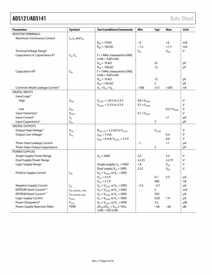
SPECIFICATIONS ELECTRICAL CHARACTERISTICS—AD5121 VDD = 2.3 V to 5.5 V, VSS = 0 V; VDD = 2.25 V to 2.75 V, VSS = −2.25 V to −2.75 V; VLOGIC = 1.8 V to 5.5 V, −40°C < TA < +125°C, unless otherwise noted.
Table 2. Parameter Symbol Test Conditions/Comments Min Typ1 Max Unit DC CHARACTERISTICS—RHEOSTAT
MODE (ALL RDACs)
Resolution N 7 Bits Resistor Integral Nonlinearity2 R-INL RAB = 10 kΩ VDD ≥ 2.7 V −1 ±0.1 +1 LSB VDD < 2.7 V −2.5 ±1 +2.5 LSB RAB = 100 kΩ VDD ≥ 2.7 V −0.5 ±0.1 +0.5 LSB VDD < 2.7 V −1 ±0.25 +1 LSB Resistor Differential Nonlinearity2 R-DNL −0.5 ±0.1 +0.5 LSB Nominal Resistor Tolerance ΔRAB/RAB −8 ±1 +8 % Resistance Temperature Coefficient3 (ΔRAB/RAB)/ΔT × 106 Code = full scale 35 ppm/°C Wiper Resistance3 RW Code = zero scale RAB = 10 kΩ 55 125 Ω RAB = 100 kΩ 130 400 Ω Bottom Scale or Top Scale RBS or RTS
RAB = 10 kΩ 40 80 Ω RAB = 100 kΩ 60 230 Ω
DC CHARACTERISTICS—POTENTIOMETER DIVIDER MODE (ALL RDACs)
Parameter Symbol Test Conditions/Comments Min Typ1 Max Unit RESISTOR TERMINALS
Maximum Continuous Current IA, IB, and IW RAB = 10 kΩ −6 +6 mA RAB = 100 kΩ −1.5 +1.5 mA Terminal Voltage Range5 VSS VDD V Capacitance A, Capacitance B3 CA, CB f = 1 MHz, measured to GND,
DIGITAL OUTPUTS Output High Voltage3 VOH RPULL-UP = 2.2 kΩ to VLOGIC VLOGIC V Output Low Voltage3 VOL ISINK = 3 mA 0.4 V ISINK = 6 mA, VLOGIC > 2.3 V 0.6 V Three-State Leakage Current −1 +1 µA Three-State Output Capacitance 2 pF
POWER SUPPLIES Single-Supply Power Range VSS = GND 2.3 5.5 V Dual-Supply Power Range ±2.25 ±2.75 V Logic Supply Range Single supply, VSS = GND 1.8 VDD V Dual supply, VSS < GND 2.25 VDD V Positive Supply Current IDD VIH = VLOGIC or VIL = GND VDD = 5.5 V 0.7 5.5 µA VDD = 2.3 V 400 nA Negative Supply Current ISS VIH = VLOGIC or VIL = GND −5.5 −0.7 µA EEPROM Store Current3, 6 IDD_EEPROM_STORE VIH = VLOGIC or VIL = GND 2 mA EEPROM Read Current3, 7 IDD_EEPROM_READ VIH = VLOGIC or VIL = GND 320 µA Logic Supply Current ILOGIC VIH = VLOGIC or VIL = GND 0.05 1.4 µA Power Dissipation8 PDISS VIH = VLOGIC or VIL = GND 3.5 µW Power Supply Rejection Ratio PSRR ∆VDD/∆VSS = VDD ± 10%,
code = full scale −66 −60 dB
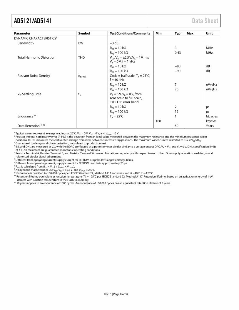
Data Sheet AD5121/AD5141
Rev. C | Page 5 of 32
Parameter Symbol Test Conditions/Comments Min Typ1 Max Unit DYNAMIC CHARACTERISTICS9
Bandwidth BW −3 dB RAB = 10 kΩ 3 MHz RAB = 100 kΩ 0.43 MHz Total Harmonic Distortion THD VDD/VSS = ±2.5 V, VA = 1 V rms,
VB = 0 V, f = 1 kHz
RAB = 10 kΩ −80 dB RAB = 100 kΩ −90 dB Resistor Noise Density eN_WB Code = half scale, TA = 25°C,
f = 10 kHz
RAB = 10 kΩ 7 nV/√Hz RAB = 100 kΩ 20 nV/√Hz VW Settling Time tS VA = 5 V, VB = 0 V, from
zero scale to full scale, ±0.5 LSB error band
RAB = 10 kΩ 2 µs RAB = 100 kΩ 12 µs Endurance10 TA = 25°C 1 Mcycles 100 kcycles Data Retention11, 12 50 Years
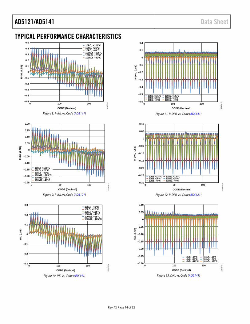
1 Typical values represent average readings at 25°C, VDD = 5 V, VSS = 0 V, and VLOGIC = 5 V. 2 Resistor integral nonlinearity (R-INL) error is the deviation from an ideal value measured between the maximum resistance and the minimum resistance wiper
positions. R-DNL measures the relative step change from ideal between successive tap positions. The maximum wiper current is limited to (0.7 × VDD)/RAB. 3 Guaranteed by design and characterization, not subject to production test. 4 INL and DNL are measured at VWB with the RDAC configured as a potentiometer divider similar to a voltage output DAC. VA = VDD and VB = 0 V. DNL specification limits
of ±1 LSB maximum are guaranteed monotonic operating conditions. 5 Resistor Terminal A, Resistor Terminal B, and Resistor Terminal W have no limitations on polarity with respect to each other. Dual-supply operation enables ground
referenced bipolar signal adjustment. 6 Different from operating current; supply current for EEPROM program lasts approximately 30 ms. 7 Different from operating current; supply current for EEPROM read lasts approximately 20 µs. 8 PDISS is calculated from (IDD × VDD) + (ILOGIC × VLOGIC). 9 All dynamic characteristics use VDD/VSS = ±2.5 V, and VLOGIC = 2.5 V. 10 Endurance is qualified to 100,000 cycles per JEDEC Standard 22, Method A117 and measured at −40°C to +125°C. 11 Retention lifetime equivalent at junction temperature (TJ) = 125°C per JEDEC Standard 22, Method A117. Retention lifetime, based on an activation energy of 1 eV,
derates with junction temperature in the Flash/EE memory. 12 50 years applies to an endurance of 1000 cycles. An endurance of 100,000 cycles has an equivalent retention lifetime of 5 years.
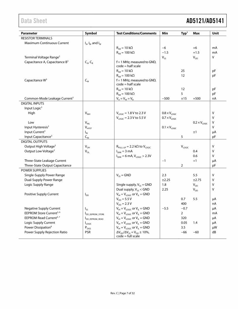
AD5121/AD5141 Data Sheet
Rev. C | Page 6 of 32
ELECTRICAL CHARACTERISTICS—AD5141 VDD = 2.3 V to 5.5 V, VSS = 0 V; VDD = 2.25 V to 2.75 V, VSS = −2.25 V to −2.75 V; VLOGIC = 1.8 V to 5.5 V, −40°C < TA < +125°C, unless otherwise noted.
Table 3. Parameter Symbol Test Conditions/Comments Min Typ1 Max Unit DC CHARACTERISTICS—RHEOSTAT
MODE (ALL RDACs)
Resolution N 8 Bits Resistor Integral Nonlinearity2 R-INL RAB = 10 kΩ VDD ≥ 2.7 V −2 ±0.2 +2 LSB VDD < 2.7 V −5 ±1.5 +5 LSB RAB = 100 kΩ VDD ≥ 2.7 V −1 ±0.1 +1 LSB VDD < 2.7 V −2 ±0.5 +2 LSB Resistor Differential Nonlinearity2 R-DNL −0.5 ±0.2 +0.5 LSB Nominal Resistor Tolerance ΔRAB/RAB −8 ±1 +8 % Resistance Temperature Coefficient3 (ΔRAB/RAB)/ΔT × 106 Code = full scale 35 ppm/°C Wiper Resistance3 RW Code = zero scale RAB = 10 kΩ 55 125 Ω RAB = 100 kΩ 130 400 Ω Bottom Scale or Top Scale RBS or RTS
RAB = 10 kΩ 40 80 Ω RAB = 100 kΩ 60 230 Ω
DC CHARACTERISTICS—POTENTIOMETER DIVIDER MODE (ALL RDACs)
Parameter Symbol Test Conditions/Comments Min Typ1 Max Unit RESISTOR TERMINALS
Maximum Continuous Current IA, IB, and IW RAB = 10 kΩ −6 +6 mA RAB = 100 kΩ −1.5 +1.5 mA Terminal Voltage Range5 VSS VDD V Capacitance A, Capacitance B3 CA, CB f = 1 MHz, measured to GND,
DIGITAL OUTPUTS Output High Voltage3 VOH RPULL-UP = 2.2 kΩ to VLOGIC VLOGIC V Output Low Voltage3 VOL ISINK = 3 mA 0.4 V ISINK = 6 mA, VLOGIC > 2.3V 0.6 V Three-State Leakage Current −1 +1 µA Three-State Output Capacitance 2 pF
POWER SUPPLIES Single-Supply Power Range VSS = GND 2.3 5.5 V Dual-Supply Power Range ±2.25 ±2.75 V Logic Supply Range Single supply, VSS = GND 1.8 VDD V Dual supply, VSS < GND 2.25 VDD V Positive Supply Current IDD VIH = VLOGIC or VIL = GND VDD = 5.5 V 0.7 5.5 µA VDD = 2.3 V 400 nA Negative Supply Current ISS VIH = VLOGIC or VIL = GND −5.5 −0.7 µA EEPROM Store Current3, 6 IDD_EEPROM_STORE VIH = VLOGIC or VIL = GND 2 mA EEPROM Read Current3, 7 IDD_EEPROM_READ VIH = VLOGIC or VIL = GND 320 µA Logic Supply Current ILOGIC VIH = VLOGIC or VIL = GND 0.05 1.4 µA Power Dissipation8 PDISS VIH = VLOGIC or VIL = GND 3.5 µW Power Supply Rejection Ratio PSR ∆VDD/∆VSS = VDD ± 10%,
code = full scale −66 −60 dB
AD5121/AD5141 Data Sheet
Rev. C | Page 8 of 32
Parameter Symbol Test Conditions/Comments Min Typ1 Max Unit DYNAMIC CHARACTERISTICS9
Bandwidth BW −3 dB RAB = 10 kΩ 3 MHz RAB = 100 kΩ 0.43 MHz Total Harmonic Distortion THD VDD/VSS = ±2.5 V, VA = 1 V rms,
VB = 0 V, f = 1 kHz
RAB = 10 kΩ −80 dB RAB = 100 kΩ −90 dB Resistor Noise Density eN_WB Code = half scale, TA = 25°C,
f = 10 kHz
RAB = 10 kΩ 7 nV/√Hz RAB = 100 kΩ 20 nV/√Hz VW Settling Time tS VA = 5 V, VB = 0 V, from
zero scale to full scale, ±0.5 LSB error band
RAB = 10 kΩ 2 µs RAB = 100 kΩ 12 µs Endurance10 TA = 25°C 1 Mcycles 100 kcycles Data Retention11, 12 50 Years
1 Typical values represent average readings at 25°C, VDD = 5 V, VSS = 0 V, and VLOGIC = 5 V. 2 Resistor integral nonlinearity error (R-INL) is the deviation from an ideal value measured between the maximum resistance and the minimum resistance wiper
positions. R-DNL measures the relative step change from ideal between successive tap positions. The maximum wiper current is limited to (0.7 × VDD)/RAB. 3 Guaranteed by design and characterization, not subject to production test. 4 INL and DNL are measured at VWB with the RDAC configured as a potentiometer divider similar to a voltage output DAC. VA = VDD and VB = 0 V. DNL specification limits
of ±1 LSB maximum are guaranteed monotonic operating conditions. 5 Resistor Terminal A, Resistor Terminal B, and Resistor Terminal W have no limitations on polarity with respect to each other. Dual-supply operation enables ground
referenced bipolar signal adjustment. 6 Different from operating current; supply current for EEPROM program lasts approximately 30 ms. 7 Different from operating current; supply current for EEPROM read lasts approximately 20 µs. 8 PDISS is calculated from (IDD × VDD) + (ILOGIC × VLOGIC). 9 All dynamic characteristics use VDD/VSS = ±2.5 V, and VLOGIC = 2.5 V. 10 Endurance is qualified to 100,000 cycles per JEDEC Standard 22, Method A117 and measured at −40°C to +125°C. 11 Retention lifetime equivalent at junction temperature (TJ) = 125°C per JEDEC Standard 22, Method A117. Retention lifetime, based on an activation energy of 1 eV,
derates with junction temperature in the Flash/EE memory. 12 50 years applies to an endurance of 1000 cycles. An endurance of 100,000 cycles has an equivalent retention lifetime of 5 years.
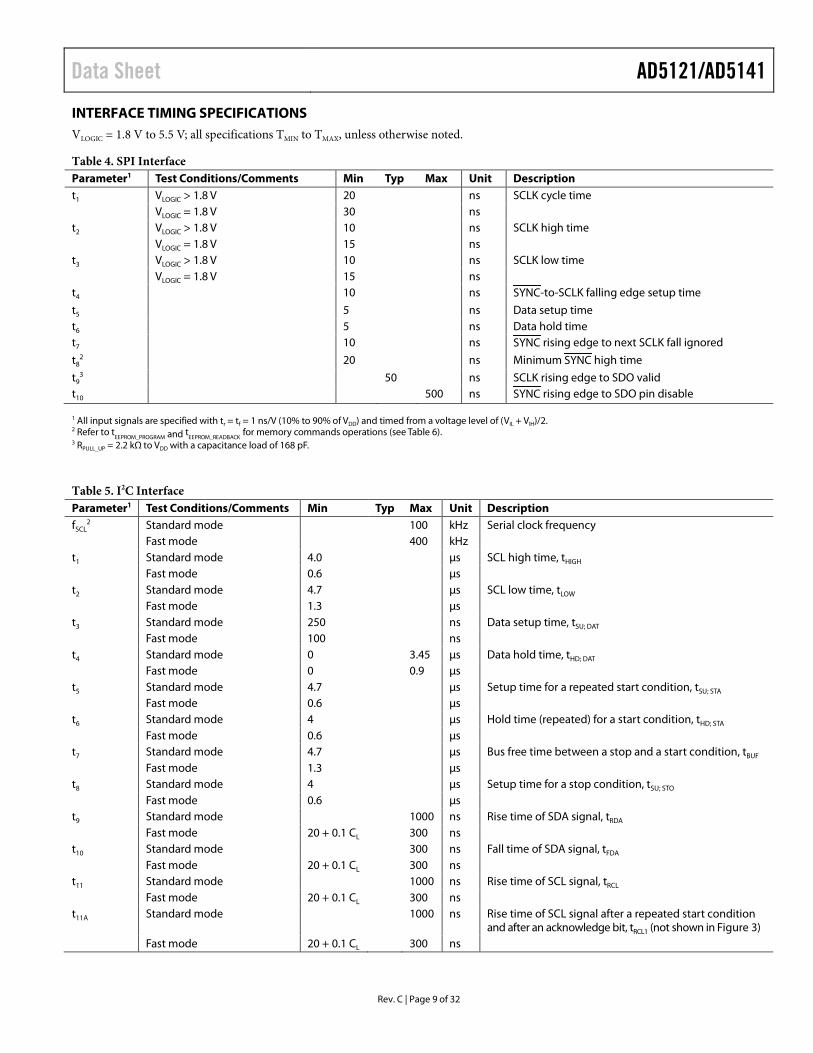
Data Sheet AD5121/AD5141
Rev. C | Page 9 of 32
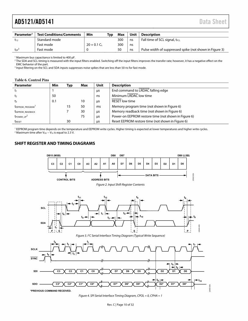
INTERFACE TIMING SPECIFICATIONS VLOGIC = 1.8 V to 5.5 V; all specifications TMIN to TMAX, unless otherwise noted.
Table 4. SPI Interface Parameter1 Test Conditions/Comments Min Typ Max Unit Description t1 VLOGIC > 1.8 V 20 ns SCLK cycle time VLOGIC = 1.8 V 30 ns t2 VLOGIC > 1.8 V 10 ns SCLK high time VLOGIC = 1.8 V 15 ns t3 VLOGIC > 1.8 V 10 ns SCLK low time VLOGIC = 1.8 V 15 ns t4 10 ns SYNC-to-SCLK falling edge setup time
t5 5 ns Data setup time t6 5 ns Data hold time t7 10 ns SYNC rising edge to next SCLK fall ignored
t82 20 ns Minimum SYNC high time
t93 50 ns SCLK rising edge to SDO valid
t10 500 ns SYNC rising edge to SDO pin disable 1 All input signals are specified with tr = tf = 1 ns/V (10% to 90% of VDD) and timed from a voltage level of (VIL + VIH)/2. 2 Refer to t
EEPROM_PROGRAM and tEEPROM_READBACK for memory commands operations (see Table 6). 3 RPULL_UP = 2.2 kΩ to VDD with a capacitance load of 168 pF.
Table 5. I2C Interface Parameter1 Test Conditions/Comments Min Typ Max Unit Description fSCL
2 Standard mode 100 kHz Serial clock frequency Fast mode 400 kHz t1 Standard mode 4.0 µs SCL high time, tHIGH Fast mode 0.6 µs t2 Standard mode 4.7 µs SCL low time, tLOW Fast mode 1.3 µs t3 Standard mode 250 ns Data setup time, tSU; DAT Fast mode 100 ns t4 Standard mode 0 3.45 µs Data hold time, tHD; DAT Fast mode 0 0.9 µs t5 Standard mode 4.7 µs Setup time for a repeated start condition, tSU; STA Fast mode 0.6 µs t6 Standard mode 4 µs Hold time (repeated) for a start condition, tHD; STA Fast mode 0.6 µs t7 Standard mode 4.7 µs Bus free time between a stop and a start condition, tBUF Fast mode 1.3 µs t8 Standard mode 4 µs Setup time for a stop condition, tSU; STO Fast mode 0.6 µs t9 Standard mode 1000 ns Rise time of SDA signal, tRDA Fast mode 20 + 0.1 CL 300 ns t10 Standard mode 300 ns Fall time of SDA signal, tFDA Fast mode 20 + 0.1 CL 300 ns t11 Standard mode 1000 ns Rise time of SCL signal, tRCL Fast mode 20 + 0.1 CL 300 ns t11A Standard mode 1000 ns Rise time of SCL signal after a repeated start condition
and after an acknowledge bit, tRCL1 (not shown in Figure 3) Fast mode 20 + 0.1 CL 300 ns
AD5121/AD5141 Data Sheet
Rev. C | Page 10 of 32
Parameter1 Test Conditions/Comments Min Typ Max Unit Description t12 Standard mode 300 ns Fall time of SCL signal, tFCL Fast mode 20 + 0.1 CL 300 ns tSP
3 Fast mode 0 50 ns Pulse width of suppressed spike (not shown in Figure 3) 1 Maximum bus capacitance is limited to 400 pF. 2 The SDA and SCL timing is measured with the input filters enabled. Switching off the input filters improves the transfer rate; however, it has a negative effect on the
EMC behavior of the part. 3 Input filtering on the SCL and SDA inputs suppresses noise spikes that are less than 50 ns for fast mode.
Table 6. Control Pins Parameter Min Typ Max Unit Description t1 1 μs End command to LRDAC falling edge
t2 50 ns Minimum LRDAC low time
t3 0.1 10 μs RESET low time
tEEPROM_PROGRAM1 15 50 ms Memory program time (not shown in Figure 6)
tEEPROM_READBACK 7 30 μs Memory readback time (not shown in Figure 6) tPOWER_UP
2 75 μs Power-on EEPROM restore time (not shown in Figure 6) tRESET 30 μs Reset EEPROM restore time (not shown in Figure 6) 1 EEPROM program time depends on the temperature and EEPROM write cycles. Higher timing is expected at lower temperatures and higher write cycles. 2 Maximum time after VDD − VSS is equal to 2.3 V.
SHIFT REGISTER AND TIMING DIAGRAMS
DATA BITS
DB8DB15 (MSB) DB0 (LSB)
D7 D6 D5 D4 D3 D2 D1 D0
ADDRESS BITS
A0A1A2C2 C1 C0 A3C3
CONTROL BITS
DB7
1094
0-00
4
Figure 2. Input Shift Register Contents
t7
t6
t2
t4
t11 t12 t6
t5t10
t1
SCL
SDA
P S S P
t3
t8
t9
1094
0-00
5
Figure 3. I2C Serial Interface Timing Diagram (Typical Write Sequence)
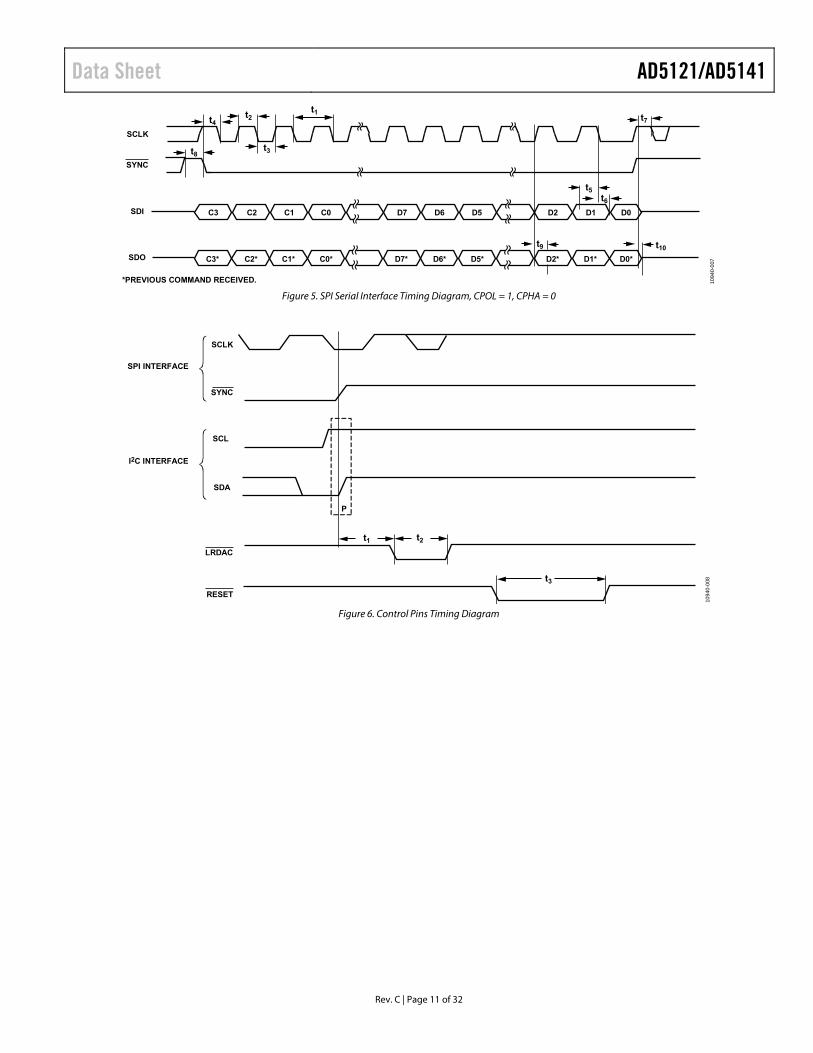
ABSOLUTE MAXIMUM RATINGS TA = 25°C, unless otherwise noted.
Table 7. Parameter Rating VDD to GND −0.3 V to +7.0 V VSS to GND +0.3 V to −7.0 V VDD to VSS 7 V VLOGIC to GND −0.3 V to VDD + 0.3 V or
+7.0 V (whichever is less) VA, VW, VB to GND VSS − 0.3 V, VDD + 0.3 V or
+7.0 V (whichever is less) IA, IW, IB
Pulsed1 Frequency > 10 kHz
RAW = 10 kΩ ±6 mA/d2 RAW = 100 kΩ ±1.5 mA/d2
Frequency ≤ 10 kHz RAW = 10 kΩ ±6 mA/√d2 RAW = 100 kΩ ±1.5 mA/√d2
Digital Inputs −0.3 V to VLOGIC + 0.3 V or +7 V (whichever is less)
Operating Temperature Range, TA3 −40°C to +125°C
Maximum Junction Temperature, TJ Maximum
150°C
Storage Temperature Range −65°C to +150°C Reflow Soldering
Peak Temperature 260°C Time at Peak Temperature 20 sec to 40 sec
Package Power Dissipation (TJ max − TA)/θJA 1 Maximum terminal current is bounded by the maximum current handling of
the switches, maximum power dissipation of the package, and maximum applied voltage across any two of the A, B, and W terminals at a given resistance.
2 d = pulse duty factor. 3 Includes programming of EEPROM memory.
Stresses at or above those listed under Absolute Maximum Ratings may cause permanent damage to the product. This is a stress rating only; functional operation of the product at these or any other conditions above those indicated in the operational section of this specification is not implied. Operation beyond the maximum operating conditions for extended periods may affect product reliability.
THERMAL RESISTANCE θJA is defined by the JEDEC JESD51 standard, and the value is dependent on the test board and test environment.
Table 8. Thermal Resistance Package Type θJA θJC Unit 16-Lead LFCSP 89.51 3 °C/W
1 JEDEC 2S2P test board, still air (0 m/sec airflow).
ESD CAUTION
Data Sheet AD5121/AD5141
Rev. C | Page 13 of 32
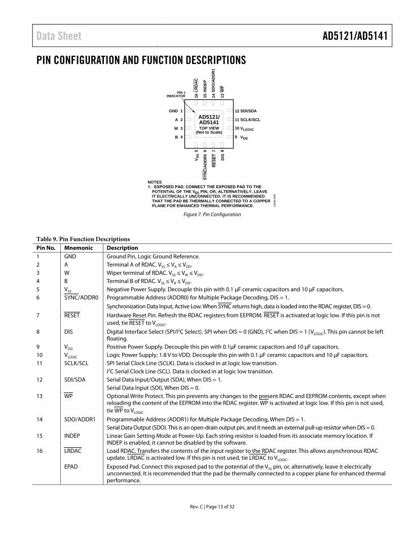
PIN CONFIGURATION AND FUNCTION DESCRIPTIONS
1094
0-00
9
AD5121/AD5141TOP VIEW
(Not to Scale)
12
11
10
1
3
4 9
2
65 7 8
16 15 14 13
GND
A
W
B
SDI/SDA
WP
SDO
/AD
DR
1
IND
EP
LRD
AC
SCLK/SCL
VLOGIC
VDD
V SS
SYN
C/A
DD
R0
RES
ET DIS
NOTES1.EXPOSED PAD. CONNECT THE EXPOSED PAD TO THE
POTENTIAL OF THE VSS PIN, OR, ALTERNATIVELY, LEAVEIT ELECTRICALLY UNCONNECTED. IT IS RECOMMENDEDTHAT THE PAD BE THERMALLY CONNECTED TO A COPPERPLANE FOR ENHANCED THERMAL PERFORMANCE.
PIN 1INDICATOR
Figure 7. Pin Configuration
Table 9. Pin Function Descriptions Pin No. Mnemonic Description 1 GND Ground Pin, Logic Ground Reference. 2 A Terminal A of RDAC. VSS ≤ VA ≤ VDD. 3 W Wiper terminal of RDAC. VSS ≤ VW ≤ VDD. 4 B Terminal B of RDAC. VSS ≤ VB ≤ VDD. 5 VSS Negative Power Supply. Decouple this pin with 0.1 µF ceramic capacitors and 10 µF capacitors. 6 SYNC/ADDR0 Programmable Address (ADDR0) for Multiple Package Decoding, DIS = 1.
Synchronization Data Input, Active Low. When SYNC returns high, data is loaded into the RDAC register, DIS = 0.
7 RESET Hardware Reset Pin. Refresh the RDAC registers from EEPROM. RESET is activated at logic low. If this pin is not used, tie RESET to VLOGIC.
8 DIS Digital Interface Select (SPI/I2C Select). SPI when DIS = 0 (GND), I2C when DIS = 1 (VLOGIC). This pin cannot be left floating.
9 VDD Positive Power Supply. Decouple this pin with 0.1µF ceramic capacitors and 10 µF capacitors. 10 VLOGIC Logic Power Supply; 1.8 V to VDD. Decouple this pin with 0.1 µF ceramic capacitors and 10 µF capacitors. 11 SCLK/SCL SPI Serial Clock Line (SCLK). Data is clocked in at logic low transition. I2C Serial Clock Line (SCL). Data is clocked in at logic low transition. 12 SDI/SDA Serial Data Input/Output (SDA), When DIS = 1. Serial Data Input (SDI), When DIS = 0. 13 WP Optional Write Protect. This pin prevents any changes to the present RDAC and EEPROM contents, except when
reloading the content of the EEPROM into the RDAC register. WP is activated at logic low. If this pin is not used, tie WP to VLOGIC
14 SDO/ADDR1 Programmable Address (ADDR1) for Multiple Package Decoding, When DIS = 1. Serial Data Output (SDO). This is an open-drain output pin, and it needs an external pull-up resistor when DIS = 0. 15 INDEP Linear Gain Setting Mode at Power-Up. Each string resistor is loaded from its associate memory location. If
INDEP is enabled, it cannot be disabled by the software. 16 LRDAC Load RDAC. Transfers the contents of the input register to the RDAC register. This allows asynchronous RDAC
update. LRDAC is activated low. If this pin is not used, tie LRDAC to VLOGIC.
EPAD Exposed Pad. Connect this exposed pad to the potential of the VSS pin, or, alternatively, leave it electrically unconnected. It is recommended that the pad be thermally connected to a copper plane for enhanced thermal performance.
Figure 38. Power Supply Sensitivity and Power Supply Rejection Ratio (PSS and PSRR)
+
–
DUT
CODE = 0x00
0.1V
VSS TO VDD
RSW =0.1VISW
ISW
W
B
A = NC
1094
0-04
5
Figure 39. Incremental on Resistance
AD5121/AD5141 Data Sheet
Rev. C | Page 20 of 32
THEORY OF OPERATION The AD5121/AD5141 digital programmable potentiometers are designed to operate as true variable resistors for analog signals within the terminal voltage range of VSS < VTERM < VDD. The resistor wiper position is determined by the RDAC register contents. The RDAC register acts as a scratchpad register that allows unlimited changes of resistance settings. A secondary register (the input register) can be used to preload the RDAC register data.
The RDAC register can be programmed with any position setting using the I2C or SPI interface (depending on the model). When a desirable wiper position is found, this value can be stored in the EEPROM memory. Thereafter, the wiper position is always restored to that position for subsequent power-ups. The storing of EEPROM data takes approximately 18 ms; during this time, the device is locked and does not acknowledge any new command, preventing any changes from taking place.
RDAC REGISTER AND EEPROM The RDAC register directly controls the position of the digital potentiometer wiper. For example, when the RDAC register is loaded with 0x80 (AD5141, 256 taps), the wiper is connected to half scale of the variable resistor. The RDAC register is a standard logic register; there is no restriction on the number of changes allowed.
It is possible to both write to and read from the RDAC register using the digital interface (see Table 16).
The contents of the RDAC register can be stored to the EEPROM using Command 9 (see Table 16). Thereafter, the RDAC register always sets at that position for any future on-off-on power supply sequence. It is possible to read back data saved into the EEPROM with Command 3 (see Table 16).
Alternatively, the EEPROM can be written to independently using Command 1 (see Table 16).
INPUT SHIFT REGISTER For the AD5121/AD5141, the input shift register is 16 bits wide, as shown in Figure 2. The 16-bit word consists of four control bits, followed by four address bits and by eight data bits
If the AD5121 RDAC or EEPROM registers are read from or written to the lowest data bit (Bit 0) is ignored.
Data is loaded MSB first (Bit 15). The four control bits determine the function of the software command, as listed in Table 11 and Table 16.
SERIAL DATA DIGITAL INTERFACE SELECTION, DIS The AD5121/AD5141 LFSCP provides the flexibility of a selectable interface. When the digital interface select (DIS) pin is tied low, the SPI mode is engaged. When the DIS pin is tied high, the I2C mode is engaged.
SPI SERIAL DATA INTERFACE The AD5121/AD5141 contain a 4-wire, SPI-compatible digital interface (SDI, SYNC, SDO, and SCLK). The write sequence begins by bringing the SYNC line low. The SYNC pin must be held low until the complete data-word is loaded from the SDI pin. Data is loaded in at the SCLK falling edge transition, as shown in Figure 4. When SYNC returns high, the serial data-word is decoded according to the instructions in Table 16.
The AD5121/AD5141 do not require a continuous SCLK when SYNC is high. To minimize power consumption in the digital input buffers when the device is enabled, operate all serial interface pins close to the VLOGIC supply rails.
SYNC Interruption
In a standalone write sequence for the AD5121/AD5141, the SYNC line is kept low for 16 falling edges of SCLK, and the instruction is decoded when SYNC is pulled high. However, if the SYNC line is kept low for less than 16 falling edges of SCLK, the input shift register content is ignored, and the write sequence is considered invalid.
SDO Pin
The serial data output pin (SDO) serves two purposes: to read back the contents of the control, EEPROM, RDAC, and input registers using Command 3 (see Table 11 and Table 16), and to connect the AD5121/AD5141 to daisy-chain mode.
The SDO pin contains an internal open-drain output that needs an external pull-up resistor. The SDO pin is enabled when SYNC is pulled low, and the data is clocked out of SDO on the rising edge of SCLK.
Daisy-chaining minimizes the number of port pins required from the controlling IC. As shown in Figure 40, the SDO pin of one package must be tied to the SDI pin of the next package. The clock period may need to be increased because of the propagation delay of the line between subsequent devices. When two AD5121/ AD5141 devices are daisy chained, 32 bits of data are required. The first 16 bits assigned to U2, and the second 16 bits assigned to U1, as shown in Figure 41. Keep the SYNC pin low until all 32 bits are clocked into their respective serial registers. The SYNC pin is then pulled high to complete the operation. A typical connection is shown in Figure 40.
To prevent data from mislocking (for example, due to noise) the device includes an internal counter, if the clock falling edges count is not a multiple of 8, the device ignores the command. A valid clock count is 16, 24, or 32. The counter resets when SYNC returns high.
I2C SERIAL DATA INTERFACE The AD5141 has 2-wire, I2C-compatible serial interface. These devices can be connected to an I2C bus as a slave device, under the control of a master device. See Figure 3 for a timing diagram of a typical write sequence.
The AD5141 supports standard (100 kHz) and fast (400 kHz) data transfer modes. Support is not provided for 10-bit addressing and general call addressing.
The 2-wire serial bus protocol operates as follows:
1. The master initiates a data transfer by establishing a start condition, which is when a high-to-low transition on the SDA line occurs while SCL is high. The following byte is the address byte, which consists of the 7-bit slave address and an R/W bit. The slave device corresponding to the transmitted address responds by pulling SDA low during the ninth clock pulse (this is called the acknowledge bit). At this stage, all other devices on the bus remain idle while the selected device waits for data to be written to, or read from, its shift register. If the R/W bit is set high, the master reads from the slave device. However, if the R/W bit is set low, the master writes to the slave device.
2. Data is transmitted over the serial bus in sequences of nine clock pulses (eight data bits followed by an acknowledge bit). The transitions on the SDA line must occur during the low period of SCL and remain stable during the high period of SCL.
3. When all data bits have been read from or written to, a stop condition is established. In write mode, the master pulls the SDA line high during the tenth clock pulse to establish a stop condition. In read mode, the master issues a no acknowledge for the ninth clock pulse (that is, the SDA line remains high). The master then brings the SDA line low before the tenth clock pulse, and then high again during the tenth clock pulse to establish a stop condition.
I2C ADDRESS The AD5141 has two different pin address options available, as shown in Table 10.
Table 10. 24-Lead LFCSP Device Address Selection ADDR0 Pin ADDR1 Pin 7-Bit I2C Device Address VLOGIC VLOGIC 0100000 No connect1 VLOGIC 0100010 GND VLOGIC 0100011 VLOGIC No connect1 0101000 No connect1 No connect1 0101010 GND No connect1 0101011 VLOGIC GND 0101100 No connect1 GND 0101110 GND GND 0101111
1 Not available in bipolar mode (VSS < 0 V) or in low voltage mode (VLOGIC = 1.8 V).
Table 11. Simple Command Operation Truth Table
Command Number
Control Bits[DB15:DB12]
Address Bits[DB11:DB8]1 Data Bits[DB7:DB0]1
C3 C2 C1 C0 A3 A2 A1 A0 D7 D6 D5 D4 D3 D2 D1 D0 Operation 0 0 0 0 0 X X X X X X X X X X X X NOP: do nothing 1 0 0 0 1 0 0 0 0 D7 D6 D5 D4 D3 D2 D1 D0 Write contents of serial register
data to RDAC 2 0 0 1 0 0 0 0 0 D7 D6 D5 D4 D3 D2 D1 D0 Write contents of serial register
data to input register 3 0 0 1 1 X 0 0 0 X X X X X X D1 D0 Read back contents D1 D0 Data 0 1 EEPROM 1 1 RDAC 9 0 1 1 1 X X 0 0 X X X X X X X 1 Copy RDAC register to EEPROM 10 0 1 1 1 X X 0 0 X X X X X X X 0 Copy EEPROM into RDAC 14 1 0 1 1 X X X X X X X X X X X X Software reset 15 1 1 0 0 0 0 0 0 X X X X X X X D0 Software shutdown D0 Condition 0 Normal mode 1 Shutdown mode 1 X = don’t care.
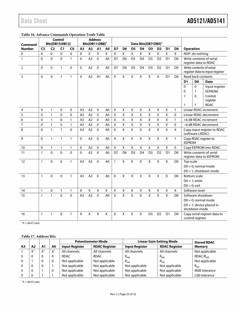
ADVANCED CONTROL MODES The AD5121/AD5141 digital potentiometers include a set of user programming features to address the wide number of applications for these universal adjustment devices (see Table 16 and Table 18).
Key programming features include the following:
• Input register • Linear gain setting mode • Low wiper resistance feature • Linear increment and decrement instructions • ±6 dB increment and decrement instructions • Burst mode (I2C only) • Reset • Shutdown mode
Input Register
The AD5121/AD5141 include one input register per RDAC register. This register allows preloading of the value for the associated RDAC register.
This feature allows a synchronous and asynchronous update of one or all the RDAC registers at the same time.
These registers can be written to using Command 2 and read back from using Command 3 (see Table 16).
The transfer from the input register to the RDAC register is done asynchronously by the LRDAC pin or synchronously by Command 8 (see Table 16).
If new data is loaded in an RDAC register, this RDAC register automatically overwrites the associated input register.
Linear Gain Setting Mode
The proprietary architecture of the AD5121/AD5141 allows the independent control of each string resistor, RAW and RWB. To enable this feature, use Command 16 (see Table 16) to set Bit D2 of the control register (see Table 18).
This mode of operation can control the potentiometer as two independent rheostats connected at a single point, W terminal, as opposed to potentiometer mode where each resistor is complementary, RAW = RAB − RWB.
This feature enables a second input and an RDAC register per channel, as shown in Table 16; however, the actual RDAC contents remain unchanged. The same operations are valid for potentiometer and linear gain setting modes.
If the INDEP pin is pulled high, the device powers up in linear gain setting mode and loads the values stored in the associated memory locations for each channel (see Table 17). The INDEP pin and D2 bit are connected internally to a logic OR gate, if any or both are 1, the devices cannot operate in potentiometer mode.
Low Wiper Resistance Feature
The AD5121/AD5141 include two commands to reduce the wiper resistance between the terminals when they achieve full scale or zero scale. These extra positions are called bottom scale, BS, and top scale, TS. The resistance between Terminal A and Terminal W at top scale is specified as RTS. Similarly, the bottom scale resistance between Terminal B and Terminal W is specified as RBS.
The contents of the RDAC registers are unchanged by entering in these positions. There are two ways to exit from top scale and bottom scale: by using Command 12 or Command 13 (see Table 16); or by loading new data in an RDAC register, which includes increment/decrement operations and a shutdown command.
Table 12 and Table 13 show the truth tables for the top scale position and the bottom scale position, respectively, when linear gain setting mode is enabled.
Table 12. Top Scale Truth Table Linear Gain Setting Mode Potentiometer Mode
RAW RWB RAW RWB RAB RAB RTS RAB
Table 13. Bottom Scale Truth Table Linear Gain Setting Mode Potentiometer Mode
RAW RWB RAW RWB RTS RBS RAB RBS
Linear Increment and Decrement Instructions
The increment and decrement commands (Command 4 and Command 5 in Table 16) are useful for linear step adjustment applications. These commands simplify microcontroller software coding by allowing the controller to send an increment or decrement command to the device. The adjustment can be individual or in a ganged potentiometer arrangement, where all wiper positions are changed at the same time.
For an increment command, executing Command 4 automatically moves the wiper to the next resistance segment position. This command can be executed in a single channel or multiple channels.
±6 dB Increment and Decrement Instructions
Two programming instructions produce logarithmic taper increment or decrement of the wiper position control by an individual potentiometer or by a ganged potentiometer arrangement where all RDAC register positions are changed simultaneously. The +6 dB increment is activated by Command 6, and the −6 dB decrement is activated by Command 7 (see Table 16). For example, starting with the zero-scale position and executing Command 6 ten times moves the wiper in 6 dB steps to the full-scale position. When the wiper position is near the maximum setting, the last 6 dB increment instruction causes the wiper to go to the full-scale position (see Table 14).
Incrementing the wiper position by +6 dB essentially doubles the RDAC register value, whereas decrementing the wiper position by −6 dB halves the register content. Internally, the AD5121/AD5141 use shift registers to shift the bits left and right to achieve a ±6 dB increment or decrement. These functions are useful for various audio/video level adjustments, especially for white LED brightness settings in which human visual responses are more sensitive to large adjustments than to small adjustments.
Table 14. Detailed Left Shift and Right Shift Functions for the ±6 dB Step Increment and Decrement Left Shift (+6 dB/Step) Right Shift (−6 dB/Step) 0000 0000 1111 1111 0000 0001 0111 1111 0000 0010 0011 1111 0000 0100 0001 1111 0000 1000 0000 1111 0001 0000 0000 0111 0010 0000 0000 0011 0100 0000 0000 0001 1000 0000 0000 0000 1111 1111 0000 0000
Burst Mode (I2C Only)
By enabling the burst mode, multiple data bytes can be sent to the device consecutively. After the command byte, the device interprets the consecutive bytes as data bytes for the first command.
A new command can be sent by generating a repeat start or by a stop and start condition.
The burst mode is activated by setting Bit D3 of the control register (see Table 18), and if a reset or power-down is performed, it automatically resets.
Reset
The AD5121/AD5141 can be reset through software by executing Command 14 (see Table 16) or through hardware on the low pulse of the RESET pin. The reset command loads the RDAC register with the contents of the EEPROM and takes approximately 30 µs. The EEPROM is preloaded to midscale at the factory, and initial power-up is, accordingly, at midscale. Tie RESET to VDD if the RESET pin is not used.
Shutdown Mode
The AD5121/AD5141 can be placed in shutdown mode by executing the software shutdown command, Command 15 (see Table 16); and by setting the LSB (D0) to 1. This feature places the RDAC in a special state. The contents of the RDAC register are unchanged by entering shutdown mode. However, all commands listed in Table 16 are supported while in shutdown mode. Execute Command 15 (see Table 16) and set the LSB (D0) to 0 to exit shutdown mode.
Table 15. Truth Table for Shutdown Mode Linear Gain Setting Mode Potentiometer Mode A2 AW WB AW WB 0 N/A1 Open Open RBS 1 Open N/A1 N/A1 N/A1
1 N/A = not applicable.
EEPROM OR RDAC REGISTER PROTECTION The EEPROM and RDAC registers can be protected by disabling any update to these registers. This can be done by using software or by using hardware. If these registers are protected by software, set Bit D0 and/or Bit D1 (see Table 18), which protects the RDAC and EEPROM registers independently.
If the registers are protected by hardware, pull the WP pin low. If the WP pin is pulled low when the device is executing a command, the protection is not enabled until the command is completed.
When RDAC is protected, the only operation allowed is to copy the EEPROM into the RDAC register.
LOAD RDAC INPUT REGISTER (LRDAC)
LRDAC software or hardware transfers data from the input register to the RDAC register (and therefore updates the wiper position). By default, the input register has the same value as the RDAC register; therefore, only the input register that has been updated using Command 2 is updated.
Software LRDAC, Command 8, allows updating of a single RDAC register or all of the channels at once (see Table 16). This is a synchronous update.
The hardware LRDAC is completely asynchronous and copies the content of all the input registers into the associated RDAC registers. If a command is executed, to avoid data corruption, any transition in the LRDAC pin is ignored by the device.
INDEP PIN If the INDEP pin is pulled high at power-up, the device operates in linear gain setting mode, loading each string resistor, RAW and RWB, with the value stored into the EEPROM (see Table 17). If the pin is pulled low, the device powers up in potentiometer mode.
The INDEP pin and the D2 bit are connected internally to a logic OR gate, if any or both are 1, the device cannot operate in potentiometer mode (see Table 18).
C3 C2 C1 C0 A3 A2 A1 A0 D7 D6 D5 D4 D3 D2 D1 D0 Operation 0 0 0 0 0 X X X X X X X X X X X X NOP: do nothing 1 0 0 0 1 0 A2 0 A0 D7 D6 D5 D4 D3 D2 D1 D0 Write contents of serial
register data to RDAC 2 0 0 1 0 0 A2 0 A0 D7 D6 D5 D4 D3 D2 D1 D0 Write contents of serial
register data to input register 3 0 0 1 1 X A2 A1 A0 X X X X X X D1 D0 Read back contents D1 D0 Data 0 0 Input register 0 1 EEPROM 1 0 Control
register 1 1 RDAC 4 0 1 0 0 A3 A2 0 A0 X X X X X X X 1 Linear RDAC increment 5 0 1 0 0 A3 A2 0 A0 X X X X X X X 0 Linear RDAC decrement 6 0 1 0 1 A3 A2 0 A0 X X X X X X X 1 +6 dB RDAC increment 7 0 1 0 1 A3 A2 0 A0 X X X X X X X 0 −6 dB RDAC decrement 8 0 1 1 0 A3 A2 0 A0 X X X X X X X X Copy input register to RDAC
(software LRDAC) 9 0 1 1 1 0 A2 0 A0 X X X X X X X 1 Copy RDAC register to
EEPROM 10 0 1 1 1 0 A2 0 A0 X X X X X X X 0 Copy EEPROM into RDAC 11 1 0 0 0 0 A2 0 A0 D7 D6 D5 D4 D3 D2 D1 D0 Write contents of serial
register data to EEPROM 12 1 0 0 1 A3 A2 0 A0 1 X X X X X X D0 Top scale D0 = 0; normal mode D0 = 1; shutdown mode 13 1 0 0 1 A3 A2 0 A0 0 X X X X X X D0 Bottom scale D0 = 1; enter D0 = 0; exit 14 1 0 1 1 X X X X X X X X X X X X Software reset 15 1 1 0 0 A3 A2 0 A0 X X X X X X X D0 Software shutdown D0 = 0; normal mode D0 = 1; device placed in
shutdown mode 16 1 1 0 1 X X X X X X X X D3 D2 D1 D0 Copy serial register data to
control register 1 X = don’t care.
Table 17. Address Bits
A3 A2 A1 A0 Potentiometer Mode Linear Gain Setting Mode Stored RDAC
Memory Input Register RDAC Register Input Register RDAC Register 1 X1 X1 X1 All channels All channels All channels All channels Not applicable 0 0 0 0 RDAC RDAC RWB RWB RDAC/RWB 0 1 0 0 Not applicable Not applicable RAW RAW Not applicable 0 0 0 1 Not applicable Not applicable Not applicable Not applicable RAW 0 0 1 0 Not applicable Not applicable Not applicable Not applicable MSB tolerance 0 0 1 1 Not applicable Not applicable Not applicable Not applicable LSB tolerance
1 X = don’t care.
AD5121/AD5141 Data Sheet
Rev. C | Page 26 of 32
Table 18. Control Register Bit Descriptions Bit Name Description D0 RDAC register write protect 0 = wiper position frozen to value in EEPROM memory 1 = allows update of wiper position through digital interface (default) D1 EEPROM program enable 0 = EEPROM program disabled 1 = enables device for EEPROM program (default) D2 Linear setting mode/potentiometer mode 0 = potentiometer mode (default) 1 = linear gain setting mode D3 Burst mode (I2C only) 0 = disabled (default) 1 = enabled (no disable after stop or repeat start condition)
Data Sheet AD5121/AD5141
Rev. C | Page 27 of 32
RDAC ARCHITECTURE To achieve optimum performance, Analog Devices, Inc., uses a proprietary RDAC segmentation architecture for all the digital potentiometers. In particular, the AD5121/AD5141 employ a three-stage segmentation approach, as shown in Figure 42. The AD5121/AD5141 wiper switch is designed with the transmission gate CMOS topology and with the gate voltage derived from VDD and VSS.
7-BIT/8-BITADDRESSDECODER
RL
W
RL
A
RH
RH RM
RM
B
RM
RM
RH
RH
STS
SBS
1094
0-04
8
Figure 42. AD5121/AD5141 Simplified RDAC Circuit
Top Scale/Bottom Scale Architecture
In addition, the AD5121/AD5141 include new positions to reduce the resistance between terminals. These positions are called bottom scale and top scale. At bottom scale, the typical wiper resistance decreases from 130 Ω to 60 Ω (RAB = 100 kΩ). At top scale, the resistance between Terminal A and Terminal W is decreased by 1 LSB, and the total resistance is reduced to 60 Ω (RAB = 100 kΩ).
PROGRAMMING THE VARIABLE RESISTOR Rheostat Operation—±8% Resistor Tolerance
The AD5121/AD5141 operate in rheostat mode when only two terminals are used as a variable resistor. The unused terminal can be floating, or it can be tied to Terminal W, as shown in Figure 43.
A
W
B
A
W
B
A
W
B
1094
0-04
9
Figure 43. Rheostat Mode Configuration
The nominal resistance between Terminal A and Terminal B, RAB, is 10 kΩ or 100 kΩ, and has 128/256 tap points accessed by the wiper terminal. The 7-bit/8-bit data in the RDAC latch is decoded to select one of the 128/256 possible wiper settings. The general equations for determining the digitally programmed output resistance between Terminal W and Terminal B are
AD5121:
WABWB RRDDR 128
)( From 0x00 to 0x7F (1)
AD5141:
WABWB RRDDR 256
)( From 0x00 to 0xFF (2)
where:
D is the decimal equivalent of the binary code in the 7-bit/8-bit RDAC register. RAB is the end-to-end resistance. RW is the wiper resistance.
In potentiometer mode, similar to the mechanical potentiometer, the resistance of the RDAC between Terminal W and Terminal A also produces a digitally controlled complementary resistance, RWA. RWA also gives a maximum of 8% absolute resistance error. RWA starts at the maximum resistance value and decreases as the data loaded into the latch increases. The general equations for this operation are
AD5121:
WABAW RRDDR
128
128)(
From 0x00 to 0x7F (3)
AD5141:
WABAW RRDDR
256
256)( From 0x00 to 0xFF (4)
where:
D is the decimal equivalent of the binary code in the 7-bit/8-bit RDAC register. RAB is the end-to-end resistance. RW is the wiper resistance.
If the device is configured in linear gain setting mode, the resistance between Terminal W and Terminal A is directly proportional to the code loaded in the associate RDAC register. The general equations for this operation are
AD5121:
WABAW RRDDR 128
)( From 0x00 to 0x7F (5)
AD5141:
WABAW RRDDR 256
)( From 0x00 to 0xFF (6)
where:
D is the decimal equivalent of the binary code in the 7-bit/8-bit RDAC register. RAB is the end-to-end resistance. RW is the wiper resistance.
In the bottom scale condition or top scale condition, a finite total wiper resistance of 40 Ω is present. Regardless of which setting the device is operating in, limit the current between Terminal A to Terminal B, Terminal W to Terminal A, and Terminal W to Terminal B, to the maximum continuous current of ±6 mA or to the pulse current specified in Table 7. Otherwise, degradation or possible destruction of the internal switch contact can occur.
Calculate the Actual End-to-End Resistance
The resistance tolerance is stored in the internal memory during factory testing. Therefore, the actual end-to-end resistance can be calculated (which is valuable for calibration, tolerance matching, and precision applications).
The resistance tolerance (in percentage) is stored in fixed point format, using a 16-bit sign magnitude binary. The sign bit (0 = negative and 1 = positive) and the integer part are located in Address 0x02, as shown in Table 19. Address 0x03 contains the fractional part, as shown in Table 19.
That is, if the data readback from Address 0x02 is 00000010, and the data readback from Address 0x03 is 10110000, the end-to-end resistance can be calculated as follows.
For Memory Map Address 0x02, DB[7] = 0 = negative, and DB[6:0] = 0000010 = 2.
For Memory Map Address 0x03, DB[7:0] = 10110000 = 176 × 2−8 = 0.6875, and therefore, tolerance = −2.6875%, and RAB = 9.731 kΩ.
PROGRAMMING THE POTENTIOMETER DIVIDER Voltage Output Operation
The digital potentiometer easily generates a voltage divider at wiper-to-B and wiper-to-A that is proportional to the input voltage at A to B, as shown in Figure 44.
W
A
B
VA
VOUT
VB 1094
0-05
0
Figure 44. Potentiometer Mode Configuration
Connecting Terminal A to 5 V and Terminal B to ground produces an output voltage at the Wiper W to Terminal B ranging from 0 V to 5 V. The general equation defining the output voltage at VW with respect to ground for any valid input voltage applied to Terminal A and Terminal B is
BAB
AWA
AB
WBW V
RDR
VR
DRDV )()()( (7)
where:
RWB(D) can be obtained from Equation 1 and Equation 2. RAW(D) can be obtained from Equation 3 and Equation 4.
Operation of the digital potentiometer in the divider mode results in a more accurate operation over temperature. Unlike the rheostat mode, the output voltage is dependent mainly on the ratio of the internal resistors, RAW and RWB, and not the absolute values. Therefore, the temperature drift reduces to 5 ppm/°C.
TERMINAL VOLTAGE OPERATING RANGE The AD5121/AD5141 are designed with internal ESD diodes for protection. These diodes also set the voltage boundary of the terminal operating voltages. Positive signals present on Terminal A, Terminal B, or Terminal W that exceed VDD are clamped by the forward-biased diode. There is no polarity constraint between VA, VW, and VB, but they cannot be higher than VDD or lower than VSS.
VDD
A
W
B
VSS 1094
0-05
1
Figure 45. Maximum Terminal Voltages Set by VDD and VSS
POWER-UP SEQUENCE Because there are diodes to limit the voltage compliance at Terminal A, Terminal B, and Terminal W (see Figure 45), it is important to power up VDD first before applying any voltage to Terminal A, Terminal B, and Terminal W. Otherwise, the diode is forward-biased such that VDD is powered unintentionally. The ideal power-up sequence is VSS, VDD, VLOGIC, digital inputs, and VA, VB, and VW. The order of powering VA, VB, VW, and digital inputs is not important as long as they are powered after VSS, VDD, and VLOGIC. Regardless of the power-up sequence and the ramp rates of the power supplies, once VLOGIC is powered, the power-on preset activates, which restores EEPROM values to the RDAC registers.
LAYOUT AND POWER SUPPLY BIASING It is always a good practice to use a compact, minimum lead length layout design. Ensure that the leads to the input are as direct as possible with a minimum conductor length. Ground paths should have low resistance and low inductance. It is also good practice to bypass the power supplies with quality capacitors. Apply low equivalent series resistance (ESR) 1 μF to 10 μF tantalum or electrolytic capacitors at the supplies to minimize any transient disturbance and to filter low frequency ripple. Figure 46 illustrates the basic supply bypassing configuration for the AD5121/AD5141.
FOR PROPER CONNECTION OFTHE EXPOSED PAD, REFER TOTHE PIN CONFIGURATION ANDFUNCTION DESCRIPTIONSSECTION OF THIS DATA SHEET.
Figure 47. 16-Lead Lead Frame Chip Scale Package [LFCSP]
3 mm × 3 mm Body and 0.75 mm Package Height (CP-16-22)
Dimensions shown in millimeters
ORDERING GUIDE Model1, 2,3 RAB (kΩ) Resolution Interface Temperature Range Package Description Package Option Branding AD5121BCPZ10-RL7 10 128 SPI/I2C −40°C to +125°C 16-Lead LFCSP CP-16-22 DHE AD5121BCPZ100-RL7 100 128 SPI/I2C −40°C to +125°C 16-Lead LFCSP CP-16-22 DHF AD5121WBCPZ10-RL7 10 128 SPI/I2C −40°C to +125°C 16-Lead LFCSP CP-16-22 DMT AD5141BCPZ10-RL7 10 256 SPI/I2C −40°C to +125°C 16-Lead LFCSP CP-16-22 DHC AD5141BCPZ100-RL7 100 256 SPI/I2C −40°C to +125°C 16-Lead LFCSP CP-16-22 DHD AD5141WBCPZ10-RL7 10 256 SPI/I2C −40°C to +125°C 16-Lead LFCSP CP-16-22 DN3 EVAL-AD5141DBZ Evaluation Board 1 Z = RoHS Compliant Part 2 The evaluation board is shipped with the 10 kΩ RAB resistor option; however, the board is compatible with both of the available resistor value options. 3 W = Qualified for Automotive Applications
AUTOMOTIVE PRODUCTS The AD5121W and AD5141W models are available with controlled manufacturing to support the quality and reliability requirements of automotive applications. Note that these automotive models may have specifications that differ from the commercial models; therefore, designers should review the Specifications section of this data sheet carefully. Only the automotive grade products shown are available for use in automotive applications. Contact your local Analog Devices account representative for specific product ordering information and to obtain the specific Automotive Reliability reports for these models.


![AT97SC3205T -SDK2 AT97SC3205P -SDK2ww1.microchip.com/.../DeviceDoc/Atmel-8528-TPM-I2C... · AT97SC3205T/3205P-SDK2 TPM I2C/SPI Development Kiti [USER GUIDE] Atmel-8528D-TPM-I2C-SPI-Development-Kit-UserGuide_052014](https://static.documents.pub/doc/80x56/5b5b7abf7f8b9a01748e2792/at97sc3205t-sdk2-at97sc3205p-at97sc3205t3205p-sdk2-tpm-i2cspi-development.jpg)


