DEPARTMENT OF THE ARMY TECHNICAL MANUAL TM 11-266 DEPARTMENT OF THE AIR FORCE TECHNICAL ORDER TO 31R1-2URR-231 Per change 4, 23 February 1978, title changed as follows: SINGLE SIDEBAND CONVERTER CV-157/URR (FIELD MAINTENANCE) (NSN 5820-00-503-2594) DEPARTMENTS OF THE ARMY AND THE AIR FORCE 21 OCTOBER 1955
Transcript
DEPARTMENT OF THE ARMY TECHNICAL MANUAL TM 11-266
DEPARTMENT OF THE AIR FORCE TECHNICAL ORDER TO 31R1-2URR-231
Per change 4, 23 February 1978, title changed as follows:
SINGLE SIDEBANDCONVERTERCV-157/URR
(FIELD MAINTENANCE)(NSN 5820-00-503-2594)
D E P A R T M E N T S O F T H E A R M Y A N D T H E A I R F O R C E
2 1 O C T O B E R 1 9 5 5
TM 11-266/T0 31R1-2URR-231
Technical Manual DEPARTMENTS OF THE ARMY ANDNo. 11-266 THE AIR FORCETechnical Order WASHINGTON 25, D. C., 21 October 1955No. 31R1-2URR-231
SINGLE SIDE BAND CONVERTER CV-157/URR
CHAPTER 1. INTRODUCTION Paragraphs PageSection I. General ..................................................................... 1, 2 3
II. Description and data.................................................. 3-7 3CHAPTER 2. THEORY ................................................................... 8-34 10
3. TROUBLESHOOTING .............................................. 35-43 434. REPAIRS .................................................................. 44-49 625. ALINEMENT.............................................................. 50-68 746. FINAL TESTING ...................................................... 69-78 887. SHIPMENT AND LIMITED STORAGE AND
DEMOLITION TO PREVENT ENEMY USESection I. Shipment and limited storage .................................... 79, 80 96
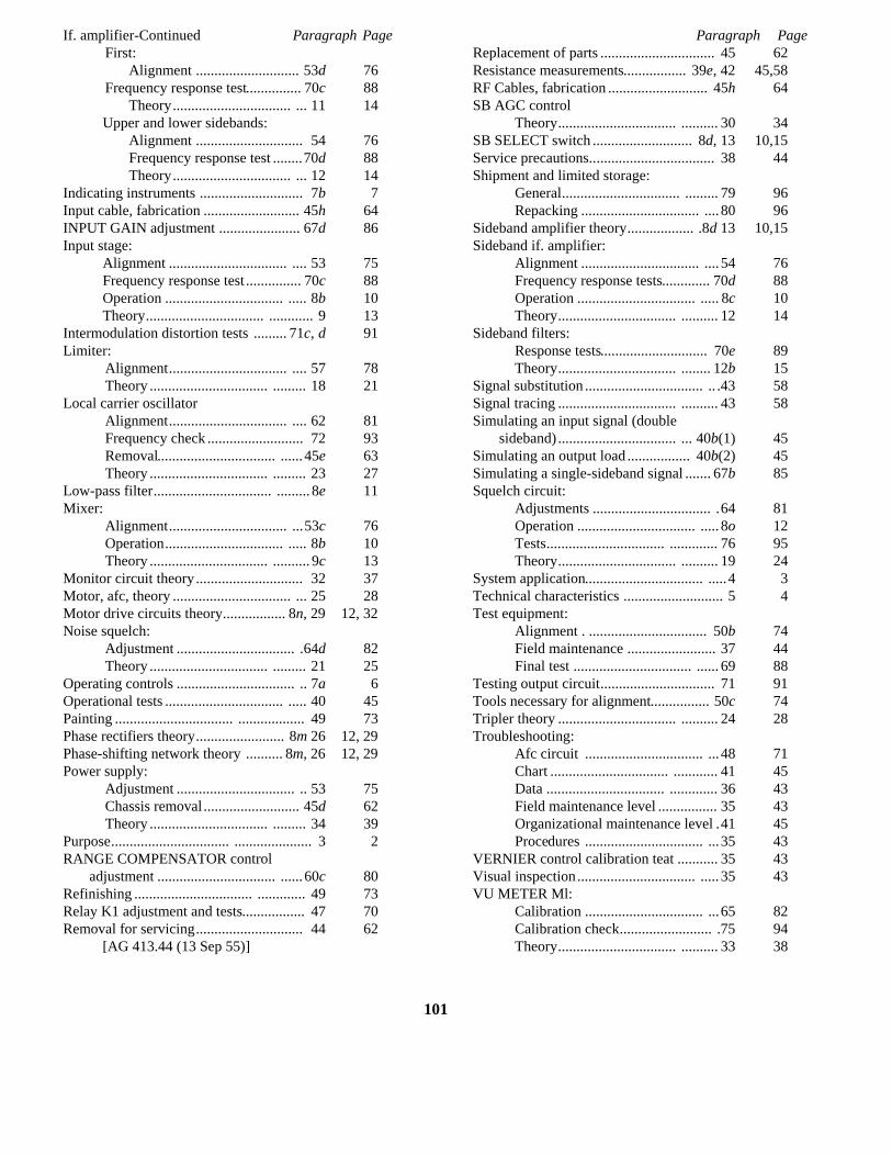
II. Demolition of materiel to prevent enemy use............. 81, 82 97INDEX .................................................................................................................... 100
}
1
CHAPTER 1INTRODUCTION
Section I. GENERAL
1. Scopea. This manual contains information on the
maintenance, alinement procedures, troubleshooting, andrepair of Single Sideband Converter CV-157/URR (fig. 1).Throughout this manual, Single Sideband Converter CV-157/URR will frequently be called the converter.
b. Forward comments on this publication directly toCommanding Officer, The Signal Corps PublicationsAgency, Fort Monmouth, New Jersey.
2. Forms and RecordsThe following forms will be used for reporting
unsatisfactory conditions of army materiel and equipmentand when performing preventive maintenance.
a. DD Form 6, Report of Damaged or ImproperShipment, will be filled out and forwarded as prescribedin SR 745-45-5 (Army), Navy Shipping Guide, Article1850-4 (Navy), and AFR 71-4 (Air Force).
b. DA Form 468, Unsatisfactory Equipment Report,will be filled out and forwarded to the Office of the ChiefSignal Officer as prescribed in SR 700-45-5.
c. DD Form 535, Unsatisfactory Report, will be filledout and forwarded to the Commanding General, AirMateriel Command, Wright-Patterson Air Force Base,Dayton, Ohio, as prescribed in SR-700-45-5 and AF TO00-35D-54.
d. Use other forms and records as authorized.
Section II. DESCRIPTION AND DATA
3. Purposea. Single Sideband Converter CV-157/URR (fig. 1) is
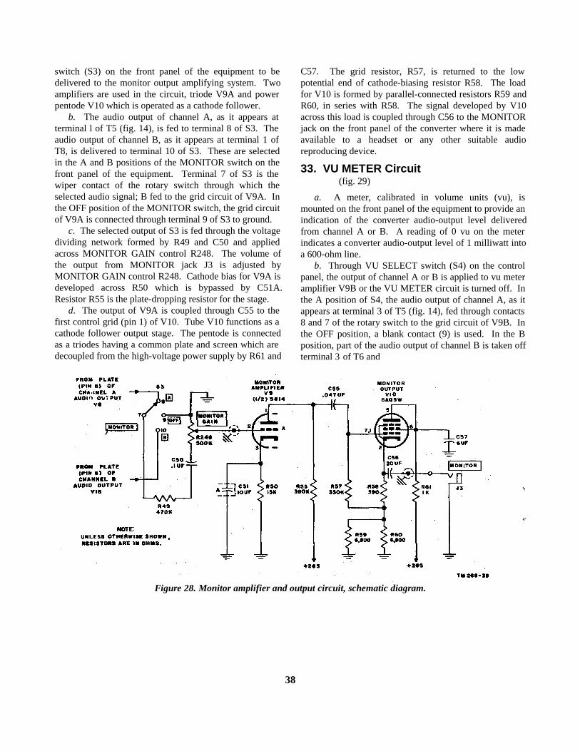
primarily intended to function as a link at the receivingend of a radio communication system using single-sideband or twin single-sideband reduced carrieremission. The converter, using the intermediate-frequency (if.) output of a communication receiver,separates the transmitted carrier frequency from itssideband frequencies and demodulates the audiointelligence present in the sidebands.
b. The converter is used also as an aid in the receptionof amplitude-modulated (am.) double-sideband signalsunder conditions of extreme atmospheric interference.
4. System Application(fig. 2)
a. The converter is intended for use in applicationsbetween fixed installations having a heavy flow ofmessage traffic. The output signal of the converter will beidentical with the multiplexed signals delivered over the
wires in voice-frequency land line carrier telephone.Thus, the converter, operating with a radio receiver, maybe used to feed carrier terminal equipment that operatesseveral channels of teletypewriter, facsimile, or voicereproducing equipment. Each of the two converter outputchannels corresponds to a pair of wires in landline voice-frequency multiplexing operations. When receiving asingle-sideband signal, the converter will deliver anoutput from a single channel that may be used to operateas many channels of teletypewriter, facsimile, or voicereproduction equipment as could be operated from acorresponding pair of wires that carry a .1- to 6-kilocycle(kc) energy spectrum and feed a single carrier terminalequipment. When twin-single side-band emission is beingused, the converter will deliver two separate channels ofoutput, thus doubling the amount of intelligence thatwould be received with a single-sideband signal. Withtwin
3
Figure 1. Single Sideband Converter CV-157/URR inoperating position.
single-sideband reception, it is possible to have onechannel used for one kind of intelligence, while thesecond channel is used for another kind of intelligence.Thus, a multiplexed teletypewriter signal can be deliveredfrom one converter channel, while the second channelhandles voice intelligence and a facsimile circuit.
b. Figure 2 illustrates a typical system that uses SingleSideband Converter CV-157/URR. A twin single-sideband signal is transmitted having eight channels ofteletypewriter intelligence in one sideband and voiceintelligence in the other sideband. A reduced carrier hasbeen included as a control signal. The transmitted signalmay lie within the range of the receiver which, in the caseof Radio Receiver R-390/URR (the intended companionreceiver for this converter) is .5 to 32 megacycles (mc).
The converter is used with Radio Sets AN/FRR-40 andAN/FRR-41. Refer to the manual on Radio Sets AN/FRR-40 and AN/FRR-41 for operation of the converter.
5. Technical CharacteristicsFrequency data:Input frequency with
converter alined assupplied.
455 kc.
Heterodyne oscillatorfrequency.
Input frequency plus 100 kc.
Input frequency range withminor readjustments.
450-510 kc.
Converter if center (local100 kc carrier oscillator)frequency.
Number of tubes_________ 44.Number of input channels_ 1.Number of output channels 2.Output data_____________ Audio-output frequency
available at terminal-board TB1 located onrear of chassis.
Monitoring facilities______ Available at MONITOR jacklocated on front panel.
Power consumption 250 watts.Weight Approx 104 lb.Audio-output level (channels
A and B).Variable between 0-100
milliwatts with 5,000microvolts or more inputfrom receiver if.
Type of frequency control__ Automatic frequency controlbased on phasecomparison. Motoroperation of heterodyneoscillator tank tuning.
4
Figure 2. Converter, system application.
Frequency data-Continued
Automatic gain control .... Selectable by the operator, to beactuated by the signal element(upper side band, lower side-band, twin sideband, receiver,and carrier) as desired. Agevoltage is applied from theconverter to control the gain inthe receiver.
Alarms:
SQUELCH ALARM.... Operates when signal-to noise ratiofalls below a predetermined level.
DRIFT ALARM .......... Actuated lust before afc circuit hasreached the end of its usefulcorrective range.
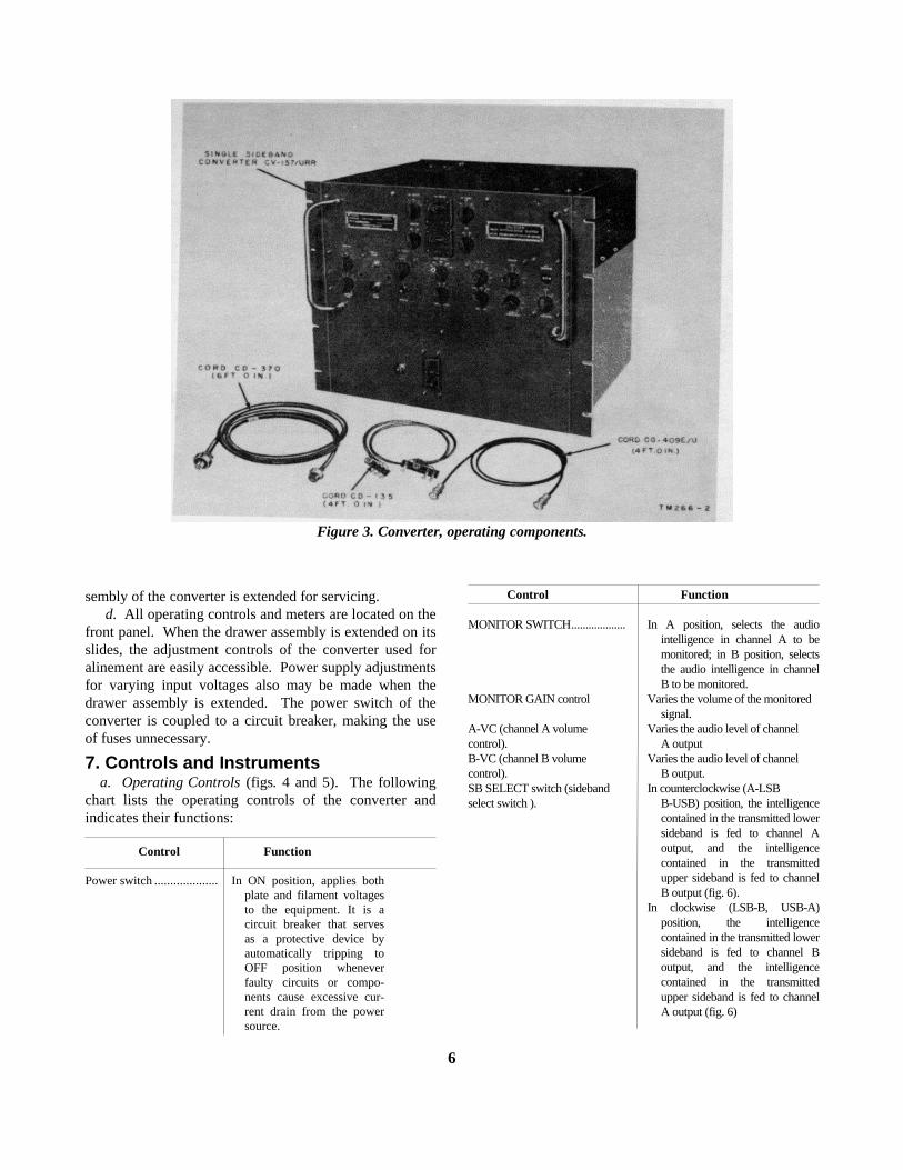
6. Descriptiona. Single Sideband Converter CV-157/URR ( fig. 3)
is a self -contained unit used for fixed installation in anystandard 19-inch relay rack.
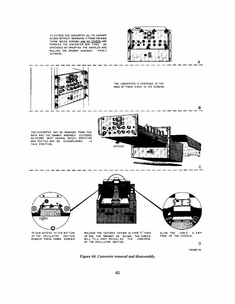
b. The converter is divided into a base assembly anda drawer assembly. The drawer assembly contains mostof the critical components of the converter. It can beextended from the base assembly on drawer slides of thefiling cabinet type so that much of the testing can beaccomplished without removing the unit from its placeof installation (C, fig. 44).
c. All input and output connections, except for themonitoring facilities, are made at the rear panel of theconverter. The MONITOR jack is located on the frontpanel. All interconnecting cables may remain in placewhen the drawer as-
5
Figure 3. Converter, operating components.
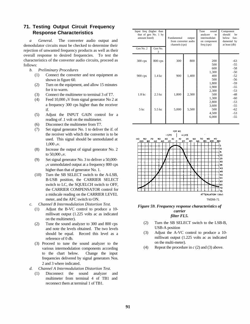
sembly of the converter is extended for servicing.d. All operating controls and meters are located on the
front panel. When the drawer assembly is extended on itsslides, the adjustment controls of the converter used foralinement are easily accessible. Power supply adjustmentsfor varying input voltages also may be made when thedrawer assembly is extended. The power switch of theconverter is coupled to a circuit breaker, making the useof fuses unnecessary.
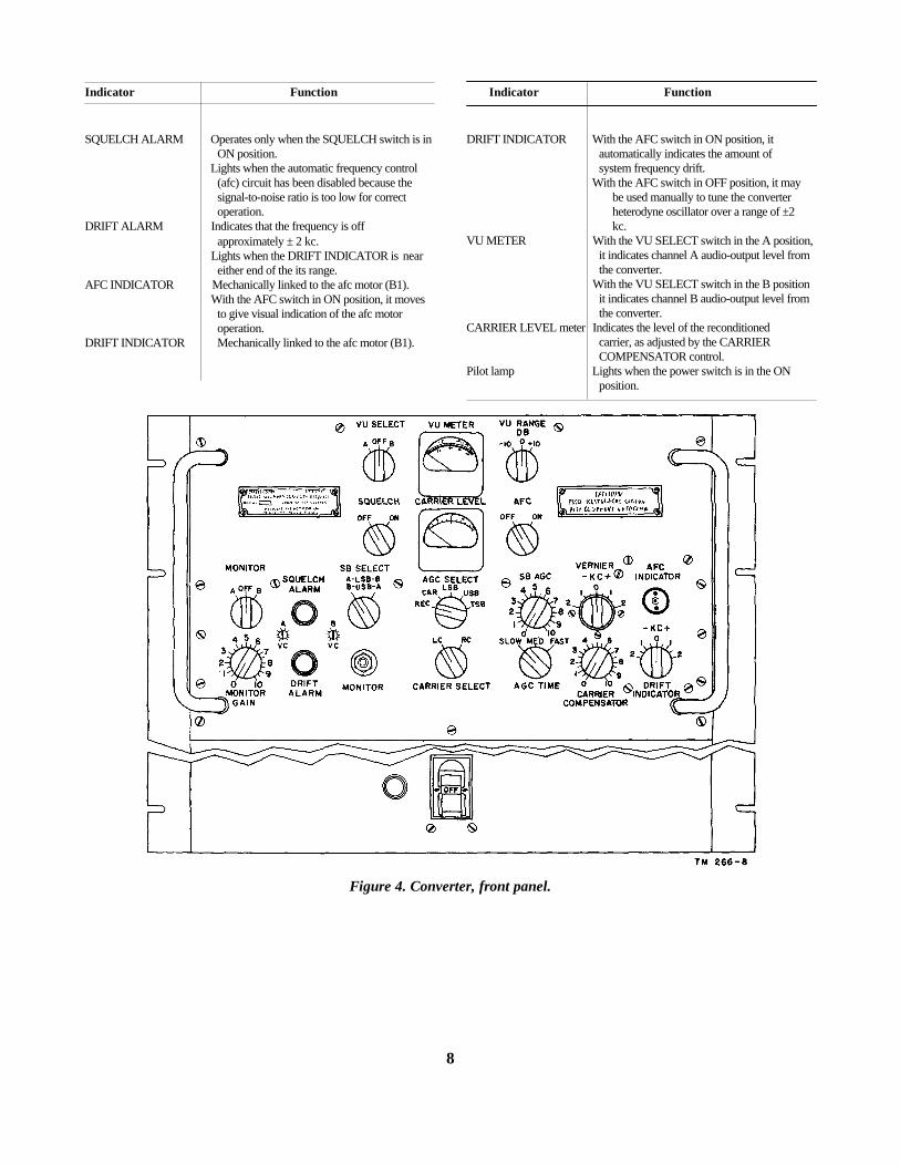
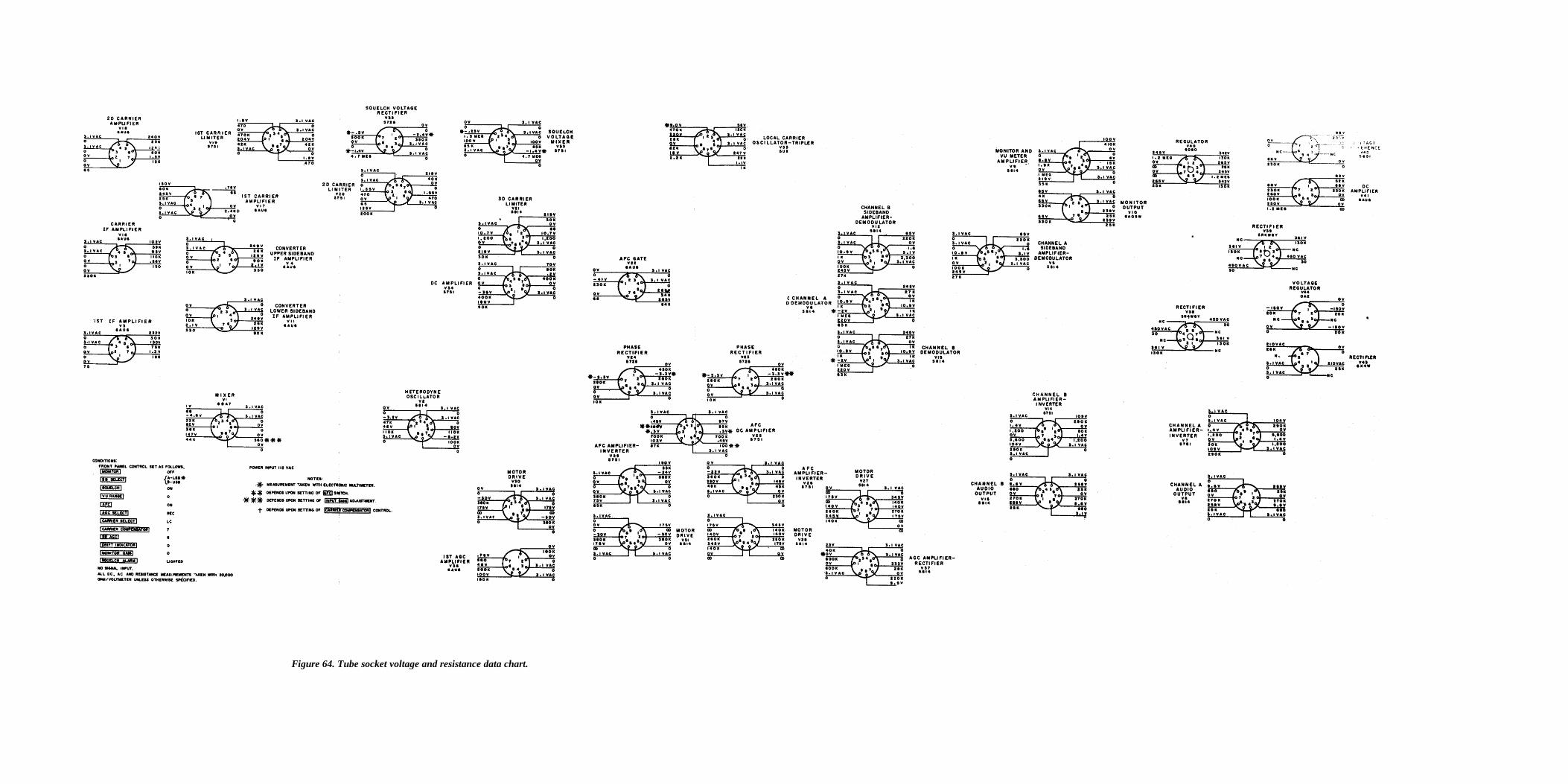
7. Controls and Instrumentsa. Operating Controls (figs. 4 and 5). The following
chart lists the operating controls of the converter andindicates their functions:
Control Function
Power switch .................... In ON position, applies bothplate and filament voltagesto the equipment. It is acircuit breaker that servesas a protective device byautomatically tripping toOFF position wheneverfaulty circuits or compo-nents cause excessive cur-rent drain from the powersource.
Control Function
MONITOR SWITCH................... In A position, selects the audiointelligence in channel A to bemonitored; in B position, selectsthe audio intelligence in channelB to be monitored.
MONITOR GAIN control Varies the volume of the monitoredsignal.
A-VC (channel A volume Varies the audio level of channelcontrol). A outputB-VC (channel B volume Varies the audio level of channelcontrol). B output.SB SELECT switch (sideband In counterclockwise (A-LSBselect switch ). B-USB) position, the intelligence
contained in the transmitted lowersideband is fed to channel Aoutput, and the intelligencecontained in the transmittedupper sideband is fed to channelB output (fig. 6).
In clockwise (LSB-B, USB-A)position, the intelligencecontained in the transmitted lowersideband is fed to channel Boutput, and the intelligencecontained in the transmittedupper sideband is fed to channelA output (fig. 6)
6
Control Function Control Function
VU SELECT switch In A position, selects channel A audio-outputlevel to be measured by the VU METER; in Bposition, selects channel B audio output to bemeasured by the VU METER.
VU RANGE switch Changes the range of the VU METERSQUELCH switch Turns squelch ON and OFF.AFC switch Turns automatic frequency control circuit ON
and OFF.AGC SELECT switch In REC (receiver) position the associated(automatic gain control receiver uses its own agc voltage, and the selectswitch) converter has no control of receiver radio-
frequency (rf) gain.In the CAR (carrier) position the 100-kc
converted carrier, with the modulation removed, is selected as the source of automatic gain control (agc), voltage developed by the converter to control the rf gain of the associated receiver.
In the LSB (lower sideband) position, the intelligence contained in the transmitted lower sideband is selected as the source ofage voltage developed by the converter tocontrol the rf gain of the associated receiver.
In USB (upper sideband) position, the intelligence contained in the transmitted upper sideband is selected as the source of agc voltage developed by the converter to control the rf gain of the associated receiver.
In TSB (twin sideband) position, the 100-kc converted carrier, plus the sidebands are selected as the source of agc voltage developed by the converter to control the rf gain of the associated receiver
CARRIER SELECT In LC position, selects the output of the local carrier switch oscillator to demodulate the intelligence present in the sideband frequenciesIn RC position, selects the reconditioned carrier
to demodulate the intelligence present in the sideband frequencies.
SB AGC control Varies the amount of agc voltage developed bythe converter when the AGC SELECT switch isin TSB, USB, or LSB position
AGC TIME switch Varies the time constant of the agc voltagedeveloped by the converter.
VERNIER control Tunes the converter heterodyne oscillator over arange of ±2 kc.
LOWPASS FILTER In IN position, limits the converter audio-outputswitch frequency band pass to 3.5 kc In OUT position,
allows frequencies as high as 6 kc to pass. This switch controls the bandwidth of both channels simultaneously.
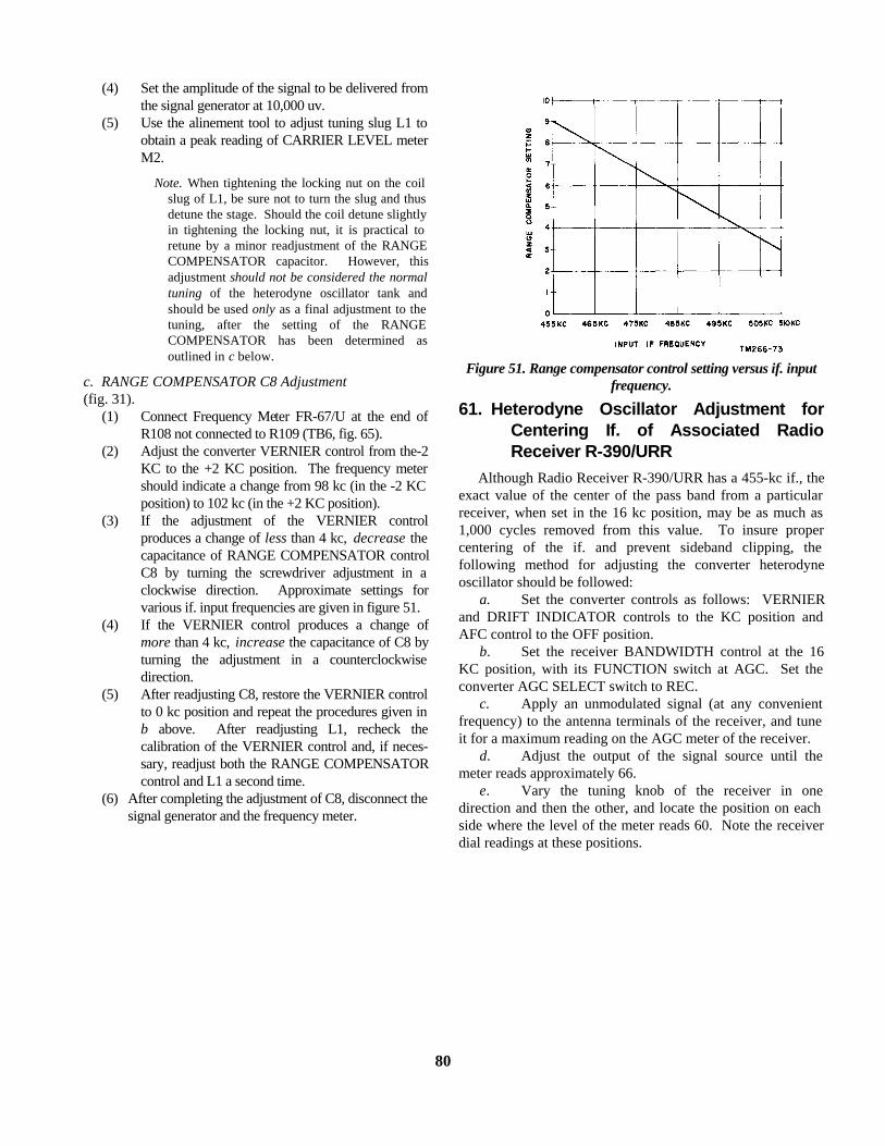
RANGE COMPENSA- Adjustment of this control corrects theTOR control calibration of the VERNIER and the
DRIFT INDICATOR controls to insure that the markings on each are accurate within200 cycles per second (cps). Refer to figure51 for approximate setting.
CARRIER COMPEN- Varies the gain of the converter carrierSATOR control section to adjust for various levels of carrier
suppression at the transmitter (fig. 53).VOLTAGE SELECT In 115V position, it selects the low-voltage
primary of the power input transformer for operation from the power source and the high amperage winding of circuit breaker CB1.In 230V position, it selects the high- voltageprimary of the power input transformer for operation from the power source and the low amperage winding of circuit breaker CB1.
Note. Front panel markings apply to the transmitted sidebandswhen the converter is used with Radio Receiver R-390/URR or areceiver having the same conversion sequence.
b. Indicating Instruments. The following chart lists the indicatinginstruments on the front panel of the converter (fig. 4) and indicatestheir functions:
7
Indicator Function Indicator Function
SQUELCH ALARM Operates only when the SQUELCH switch is inON position.
Lights when the automatic frequency control(afc) circuit has been disabled because thesignal-to-noise ratio is too low for correctoperation.
DRIFT ALARM Indicates that the frequency is off approximately ± 2 kc.
Lights when the DRIFT INDICATOR is near either end of the its range.
AFC INDICATOR Mechanically linked to the afc motor (B1).With the AFC switch in ON position, it moves
to give visual indication of the afc motoroperation.
DRIFT INDICATOR Mechanically linked to the afc motor (B1).
DRIFT INDICATOR With the AFC switch in ON position, it automatically indicates the amount of system frequency drift.
With the AFC switch in OFF position, it may be used manually to tune the converter heterodyne oscillator over a range of ±2 kc.
VU METER With the VU SELECT switch in the A position, it indicates channel A audio-output level from the converter.
With the VU SELECT switch in the B position it indicates channel B audio-output level from the converter.
CARRIER LEVEL meter Indicates the level of the reconditioned carrier, as adjusted by the CARRIER COMPENSATOR control.
Pilot lamp Lights when the power switch is in the ON position.
Figure 4. Converter, front panel.
8
Figure 5. Converter, rear view.
Figure 6. Positions of SB SELECT switch.
TM266-9
9
TM 266-58Figure 7. Converter, block diagram.
CHAPTER 2
THEORY
8. Block Diagrama. General. In the block diagram (fig. 7), the
following circuits have been included in Single SidebandConverter CV-157/URR.
(1) Monitor circuits. A VU METER and a monitoraudio-output circuit are included in theconverter to facilitate audio-output leveladjustments and tuning operations.
(2) Afc circuit. This circuit controls the frequencyof the converter heterodyne oscillator andholds the converter if. at exactly 100 kc. Thiscompensates for frequency drifts in thereceiver, transmitter, and converter. Thiscircuit assures an extremely accurate audio-frequency (af) output from the converter.
(3) Squelch circuit. The squelch circuitautomatically disables the afc circuit when thesignal-to-noise ratio of the converter inputsignal drops below a certain preselected level.The squelch circuit prevents the afc circuitfrom being actuated by noise instead of signal,which would result in the converter beingdetuned.
(4) Local carrier oscillator. This circuit provides aconstant amplitude, noise-free carrierfrequency for use in the converterdemodulators. It also provides a frequencystandard against which the incoming carrier iscompared for operating the afc circuit.
(5) Agc circuit. This circuit enables the converteroperator to control the receiver gain from anyof the separated signal elements in theconverter. Through proper use of the agccircuit, the operator is assured a constantamplitude for that part of the signal in whichthe amplitude is most critical.
b. Input Circuit. The output of the receiver if. amplifieris applied at J1 of the converter and mixed in V1 with theoutput of the converter heterodyne oscillator, V2. The
output of V2 is 555 kc which, when beat against the 455-kc output of the receiver if., produces a converter if. of100 kc. The sideband frequencies appear above and belowthis converted carrier frequency, which is delivered to thefirst if. amplifier, V3.
c. Sideband If. Amplifier and Filter Circuits. Theoutput of V3 is delivered to three additional if. amplifiers,two of which (V4 and V11) are used to amplify the signalfurther for delivery to the converter upper and lowersideband filters, FL1 and FL3. Filter FL1 separates theconverter upper sideband frequency elements from the if.signal output of V4, which because of sideband inversion,were originally the transmitted lower sideband frequencyelements. The sideband filters are selective and thefrequencies above and below the sideband elements aresharply attenuated. The converter lower sideband filter,FL3, functions similarly to FL1, separating the converterlower sideband frequency elements from the if. signal thatis fed to it from amplifier V11.
d. SB SELECT Switch and Sideband Amplifiers. Theoutputs of the two sideband filters are delivered to SBSELECT switch S1. The operator selects the converteraudio-output channel that will deliver the intelligence inthe converter upper sideband and the channel that deliversthe intelligence in the converter lower sideband. Theswitch selects the output of each of the sideband filters tobe fed to the channel A or channel B. sideband amplifier.The switch is marked so that the output of the converterlower sideband is delivered through channel B. in the A-LSB, B-USB position of S1. This is because the markingson the switch refer to the sidebands of the transmittedsignal when the signal is received in Radio Receiver R-390/URR or any other receiver having a similarconversion sequence. Where the transmitted side-bandsare inverted as a result of heterodyning in some other typeof receiver, the markings of the SB SELECT switch nolonger apply to the sidebands of the transmitted signal.From the SB SELECT switch, the signals are fed tochannel A sideband amplifier V5A
10
and channel B sideband amplifier V12A, where the signalstrength is further increased preparatory to demodulation.
e. Channel A Demodulators. Three triode sections,V5B, V6A, and V6B, are used in the channel Ademodulator circuit to serve the dual functions of audiodetection and amplification. The sideband frequencyoutput of V5A is delivered to the demodulator stageswhere it is mixed with the 100-kc output signal of eitherthe third carrier limiter or the local carrier oscillator,depending on the setting of the CARRIER SELECTswitch, S6. The resultant mixture consists of manydifferent frequencies, including the sideband frequencyminus the carrier frequency which is an audio beatfrequency that contains the audio intelligence with whichthe transmitted signal was originally modulated. Thisdesired information is retained, while rejecting theunwanted mixing products in filter networks passing onlythe audio frequencies. A resistance capacitance networkin each channel attenuates the sum frequencies (above 100kc). Frequency components around 100 kc are sharplyattenuated by a tuned 100-kc trap. A low-filter rejectsaudio frequencies above 3.5 kc. The operator, throughLOWPASS FILTER switch S2, selects either that the 100-kc trap or the low-pass filter be placed in the outputcircuit of the demodulator. The filter used depends on thecharacter of the transmitted signal. Multiplex tele-typewriter signals transmitted, using audio frequencydiversity, have a bandwidth of about 6 kc. For this type ofsignal, S2 is placed in the OUT position so that the 100-kcbypass filter is in the output circuit of the demodulatorstages. The demodulators in both channels are identicalin circuit and operation.
f. Audio-inverter and Audio-output Stages. The outputstages of each channel, consisting of V7 and V8 inchannel A and V14 and V15 in channel B, provide theinverter-amplifier arrangement necessary to deliver apush-pull audio output from the two channels of theconverter.
g. Carrier If. Amplifier and Filter Circuits. The outputof first if. amplifier V3 is delivered to the carrier and thesideband amplifying strips. Carrier if. amplifier V16amplifies the if. signal before it is fed to the sharplypeaked 100-kc carrier filter, FL5. Filter FL5 removes thesideband frequencies from the if. signal, delivering only100 kc to first carrier amplifier V17.
h. Carrier Amplifiers. Following FL5, two amplifiers,V17 and V18, are used to amplify the 100-kc signal.These amplifiers are needed in the carrier section of theequipment because the normally received signal will havethe carrier frequency reduced below the level of thereceived sideband frequencies.
i. Carrier Limiter Stages. The output of the secondcarrier amplifier is fed to a series of three limiters, V19,V20, and V21, which maintain a constant carrieramplitude by removing the amplitude variations caused byfading. After limiting, the carrier is ready for delivery tothe afc circuit and, if necessary, to the demodulatorcircuits.
j. AGC SELECT Switch S10. The converter is equippedwith an agc circuit that applies agc voltage to the receiver.This circuit enables a constant amplitude signal to be fedfrom the converter to the terminal equipment. Thereceiver agc circuit operates on amplitude of its over-allinput signal. Thus, when one sideband is used to transmitvoice while the other sideband carries a multiplexteletypewriter signal, the receiver agc circuit is affected bythe voice signal. Under these conditions, the receiver agccircuit produces a very erratic output from the converterchannel that delivers the demodulated multiplexteletypewriter signal to terminal equipment. Noise andextraneous signals also have an adverse effect on thereceiver agc system. For this reason, the converter isprovided with a selector switch through which theoperator may select the receiver agc system from voltagesdeveloped at a variety of points throughout the converter.AGC SELECT switch S10 (fig. 7) is a five-positionswitch. In the REC position, the converter has no controland the receiver agc system operates as it normally wouldfor the overall signal received. This position is used fortuning and adjustment operations and may also be usedwhen the converter agc circuit fails, but continuedoperation of the system is necessary. In the CAR position,the receiver agc system is controlled by the output of the100-kc carrier filter, FL5. This position of the switch isused when receiving a standard am. signal or when onlyspeech information is transmitted in the sidebands. In theUSB and LSB positions, the output of the converter lowersideband filter FL3 or the converter upper sideband filterFL1, respectively,
11
is used to control the receiver age. The converter frontpanel designations refer to the transmitted sidebandrelationships when the converter is used with RadioReceiver R-390/URR. Either the LSB or USB position ofS10 is used when keyed-tone intelligence is received inone converter channel, as some signal of widely varyingamplitude (such as a voice signal) is received in the otherchannel. In the TSB position, the age control signal istaken off the output of first if. amplifier V3. This positionof S10 is used when keyed-tone intelligence (or anyintelligence of constant amplitude) is received in bothconverter channels. This position is superior to the RECposition for this type of signal, because the if. strip in thereceiver and the tuned outputs of V1 and V3 largelyeliminate the adverse effects noise and interfering signalshave on the receiver agc system
k. Agc Output Circuit. The converter age outputcircuit consists of two amplifiers V36 and V37A, and arectifier, V37B. The voltage selected by S10 is amplifiedin V36 and V37A, rectified to a direct-current (dc) voltagein V37B, and then fed to the receiver
l. Afc Gate. Afc gate tube V22 triples the outputfrequency of the third carrier limiter for delivery to the afccircuit. When biased beyond cutoff by a voltage appliedfrom the squelch circuit, the gate effectively prevents tileoutput of the third limiter from reaching the afc circuit toprevent the circuit being actuated by noise.
m. Phasing Network and Phase Rectifiers. Theoutput of afc gate V22 and tripler V35B is fed to phaserectifiers V23 and V24. Rectifier V23 has a phase-shifting network in its plate circuit, which insures that anyoutput from the two rectifiers will be 90° out of phase. Inthe on frequency condition, the outputs of V22 and V36Bproduce no error outputs voltage from the phase rectifiersAs soon as transmitter, receiver, or converter Frequencydrift causes a difference between the outputs of V35B andV22, the rectifiers begin to conduct to produce polarizedsignal outputs, one from each rectifier, which are 90° outof phase with one another. Afc dc amplifier V25 is a dualtriode. Each half amplifies the output of one of the phaserectifiers
n. Afc Amplifier-inverter and Motor Drive Stages.The output of V25A is fed to V26A; the output of V25B isfed to V29A. Tubes V26 and V29 are dual triodes,operating push-pull into the motor drive amplifiers, V27through V31 which are connected across the windings of
motor B1. Tube V26 controls the operation of motordrive stages V27 and V28 Tube V29 controls theoperation of motor drive stages V30 and V31. Motor B1is a drag cup motor that runs when a voltage is appliedacross one winding which is 90° out of phase with thatapplied across the other winding. The function of theamplifier-inverter and motor drive stages is to amplify theoutput of the phase rectifiers to a current and voltagenecessary to cause B1 to react to the phase differenceexisting between the outputs of the rectifiers. The motorcontrols a variable capacitor located in the tank circuit ofthe converter heterodyne oscillator (V2) so that theconverter if. is again returned to 100 kc. When thecorrect converter if. is once more restored, there ceases tobe an output developed at the phase rectifiers and the afccircuit is returned to a rest condition
o. Squelch Circuit. Regardless of the elaboratefiltering, amplifying, and limiting to which the convertedcarrier frequency is subjected before it is applied to the afccircuit, it is still possible under extremely unfavorableconditions of reception, for noise to become the dominantoutput of the carrier strip. This would result in erraticoperation of the afc circuit and subsequent loss of a usableconverter audio output. To prevent erratic operation ofthe afc circuit, a squelch circuit is provided to measureautomatically the signal-to-noise ratio existing in thecarrier strip and to disable the afc circuit when its properoperation is endangered through the introduction of noiseinto the circuit. Figure 7 shows that rectifiers V32A andV32B are used to feed a mixer which, in turn, feeds anamplifier. Rectifier V32A measures the signal strengthdelivered through the carrier strip for operating thesquelch circuit and as a source of rectified voltage for theoperation of the CARRIER LEVEL METER. RectifierV32A also allows the afc circuit to operate when thestrength of any signal (noise, as well as carrier) present atthe input of the first limiter is of a certain predeterminedlevel. Noise rectifier V32B operates from a filter locatedin the plate circuit of second carrier limiter V20. Thefilter acts as a block to the 100-kc signal component in thelimiter strip, but passes any noise present in the output ofthe second limiter. When the rectifier noise voltagedelivered to mixer V33 rises above a certain value, afcgate V22 is cut off through amplifier V34. ThroughV32A and V32B, excessive noise and in-
12
adequate signal strength are detected and used to drive theafc gate beyond the cutoff point to prevent the delivery ofthe third limiter output to the afc circuit .
9. Input Stage(fig. 8)
a. An if. of 455 kc is delivered from the receiver toconverter IF. INPUT jack J1. Adjustments are providedso that the converter may be used with any receiver thathas an if. output within the range of 450 to 510 kc. In thisand the other theory paragraphs that follow, it is assumedthat the converter is used with Radio Receiver R-390/URR, or equivalent, which has an if. output of 455 kc.
b. The input signal to the converter is applied acrosscoaxial line terminating resistor R1 and control R2.INPUT GAIN adjustment control R2 enables efficientmixing to take place in V1, when the converter is usedwith receivers that have various if. output amplitudes.
c. Mixer V1 combines the 455-kc output of the receiverwith the 555-kc output of the converter heterodyneoscillator to produce the converter if. of 100 kc. Theinjection voltage, which is developed across R2, is appliedto the second control grid (pin 7) of V1. The output of theconverter heterodyne oscillator is coupled through C1 andapplied to the first control grid (pin. 2) of V1. The platecircuit of V1 is tuned to select the difference between themixer 455- and 555-kc inputs, and reject other unwantedfrequencies produced in the tube. The plate current of V1
flows through the slug-tuned primary of if. transformerT1. This primary inductance, in parallel with tuningcapacitors C21 and C73, provides a plate load resonant at100 kc, when the slug core is correctly adjusted. The slugcore of the transformer secondary provides a couplingadjustment. Fixed capacitor C22 and trimmer C23resonate the transformer secondary.
d. The mixer develops cathode bias across R4, which isbypassed through C2. Resistors R2 and R3 return thegrids to ground. The screen voltage is held at the requireddc potential by dropping resistor R5, which is bypassed byC4. Plate voltage for V1 is applied through R6, which isbypassed by C5. The decoupling network formed by R11and C3 effectively prevents any rf. at the plate and screenof V1 from reaching the converter high-voltage powersupply.
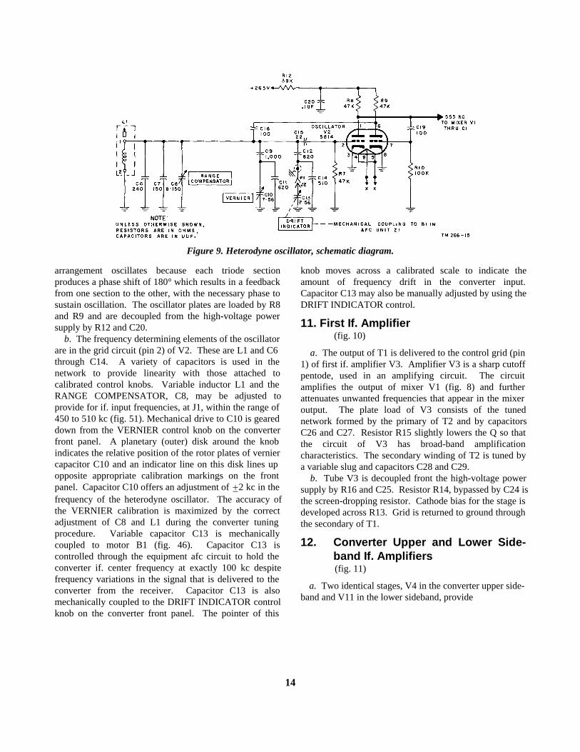
10. Heterodyne Oscillator(fig. 9)
a. Oscillator V2 uses a dual triode in a modifiedmultivibrator circuit. The circuit is a two-stage capacity-resistance-coupled amplifier that feeds back on itself tosustain oscillation. A very small positive voltage, appliedto the control grid (pin 2) of V2, is amplified, coupledthrough C19 and appears at the grid (pin 7) of V2. Thesignal is further amplified and feedback is achievedthrough C16 and C15 to the grid (pin 2) of V2. Such an
Figure 8. Input and mixer stage, schematic diagram.
arrangement oscillates because each triode sectionproduces a phase shift of 180° which results in a feedbackfrom one section to the other, with the necessary phase tosustain oscillation. The oscillator plates are loaded by R8and R9 and are decoupled from the high-voltage powersupply by R12 and C20.
b. The frequency determining elements of the oscillatorare in the grid circuit (pin 2) of V2. These are L1 and C6through C14. A variety of capacitors is used in thenetwork to provide linearity with those attached tocalibrated control knobs. Variable inductor L1 and theRANGE COMPENSATOR, C8, may be adjusted toprovide for if. input frequencies, at J1, within the range of450 to 510 kc (fig. 51). Mechanical drive to C10 is geareddown from the VERNIER control knob on the converterfront panel. A planetary (outer) disk around the knobindicates the relative position of the rotor plates of verniercapacitor C10 and an indicator line on this disk lines upopposite appropriate calibration markings on the frontpanel. Capacitor C10 offers an adjustment of 2 kc in thefrequency of the heterodyne oscillator. The accuracy ofthe VERNIER calibration is maximized by the correctadjustment of C8 and L1 during the converter tuningprocedure. Variable capacitor C13 is mechanicallycoupled to motor B1 (fig. 46). Capacitor C13 iscontrolled through the equipment afc circuit to hold theconverter if. center frequency at exactly 100 kc despitefrequency variations in the signal that is delivered to theconverter from the receiver. Capacitor C13 is alsomechanically coupled to the DRIFT INDICATOR controlknob on the converter front panel. The pointer of this
knob moves across a calibrated scale to indicate theamount of frequency drift in the converter input.Capacitor C13 may also be manually adjusted by using theDRIFT INDICATOR control.
11. First If. Amplifier(fig. 10)
a. The output of T1 is delivered to the control grid (pin1) of first if. amplifier V3. Amplifier V3 is a sharp cutoffpentode, used in an amplifying circuit. The circuitamplifies the output of mixer V1 (fig. 8) and furtherattenuates unwanted frequencies that appear in the mixeroutput. The plate load of V3 consists of the tunednetwork formed by the primary of T2 and by capacitorsC26 and C27. Resistor R15 slightly lowers the Q so thatthe circuit of V3 has broad-band amplificationcharacteristics. The secondary winding of T2 is tuned bya variable slug and capacitors C28 and C29.
b. Tube V3 is decoupled front the high-voltage powersupply by R16 and C25. Resistor R14, bypassed by C24 isthe screen-dropping resistor. Cathode bias for the stage isdeveloped across R13. Grid is returned to ground throughthe secondary of T1.
12. Converter Upper and Lower Side-band If. Amplifiers(fig. 11)
a. Two identical stages, V4 in the converter upper side-band and V11 in the lower sideband, provide
14
Figure 10. First if. amplifier, schematic diagram.
the necessary injection voltage for a satisfactory outputvoltage from sideband filters FL1 and FL3. The converterupper sideband will be discussed fully in this section; itdiffers from the lower sideband only in the frequenciesinvolved. The if. output of T2 is coupled to the controlgrid (pin 1) of V4 through C30 and R17. The input signalis dropped across the L-pad, formed by resistors R17 andR18, which isolates the amplifier from the three otherstages fed by T2. Tube V4 is a sharp cutoff pentode; theplate load is tuned by the network comprising the primaryof T3, capacitor C34, and trimmer C33. Trimmer C33 isadjusted so that the network is peaked at 104 kc. Theoutput curve of the transformer is flat across the uppersideband frequencies, with very little file attenuation tocarrier and lower sideband frequencies. Resistor R21lowers the Q in the tuned circuit, providing for wide-bandamplification in V4.
b. The output from the secondary of T3 is delivered intoresistive padding network R23, R25, R27, R26, R24, andR28. This network provides the correct input impedanceto upper sideband filter FL1, and also isolates the filter toprevent detuning and other undesirable effects. Filter FL1is a band-pass filter that allows the frequencies between100.1 and 106 kc to pass freely, and attenuates sharply allother frequencies.
c. The output of FL1, which consists of the converterupper sideband frequencies, is delivered, through padresistors R260 and R261, across impedance-matchingresistors R29 and R30 to the untuned primary of T4.Proper impedance matching at input and output of eachfilter insures best band-pass characteristics. The secondaryof T4, also untuned, has one side grounded, while theother side is connected to SB SELECT switch S1 (fig. 12).
d. Tube V4 develops cathode bias across R19. Thescreen of the amplifier is decoupled from the high-voltagepower supply by network R20, C31, and C32. The platedropping resistor for the stage is R22.
e. In the lower sideband, V11 and its associatedcomponents perform identical functions with those in theupper sideband, except that the frequencies selected by T6and FL3 lie in the range of 94 to 99.9 kc. Thesefrequencies are the converter lower sideband frequenciesthat correspond to the transmitted upper sidebandfrequencies. An additional capacitor, C62, is placedacross the primary of the output transformer of V11.Capacitor C62 enables the transformer to be tuned to thelower frequencies that are desired as an input for FL3.
13. Channels A and B SidebandAmplifiers(fig. 12)
a. The outputs of upper and lower sideband filters FL1and FL3 are applied through T4, T7, and SB SELECTswitch S1 to channels A and B sideband amplifiers V5Aand V12A, respectively.
b. The intelligence delivered at the channels A and Boutputs is selected by the position of SB SELECT switchS1. This switch has two positions, A-LSB, B-USB andLSB-B, USB-A. These markings refer to the sidebandfrequencies as transmitted, when the converter is usedwith Radio Receiver R-390/URR or any receiver with anequivalent system of input frequency conversion.
c. Because of the reversal of frequency relationshipscaused by the converter input signal heterodyning, S1selects the converter upper side-
15
Figure 11. Sideband if. amplifiers and filters, schematic diagram.
16
Figure 12. Channel and B sideband amplifiers, schematic diagram.
band frequencies to be delivered to channel A, and theconverter lower sideband frequencies to be delivered tochannel B in the A-LSB, B-USB position. In figure 12,switch S1 is shown in the A-LSB, B-USB position. Theconverter upper sideband frequencies are applied from T4to contact 11 of S1, through the switch rotating element tocontact 2, and to the control grid (pin 7) of channel Asideband amplifier V5A. Simultaneously, the output ofT7, which consists of the converter lower sidebandfrequencies, is applied to contact 5 of S1, through anotherrotating element, to pin 8 of the switch, and to the controlgrid (pin 7) of channel B sideband amplifier V12A.When the switch is placed in the LSB-B, USB-A position,the elements are rotated so that the converter uppersideband frequencies are applied through contacts 11 and8 to pin 7 of V12A. The lower sideband frequencies areapplied through contacts 5 and 2 to pin 7 of V5A.
d. Sideband amplifiers V5A and V12A are Class Atriode amplifiers, which amplify the sideband frequenciesbefore they are applied to the demodulator stages. Inchannel A the output of V5A is applied across loadresistor R32 and is coupled to the next stage throughcapacitor C36. The plate is decoupled from the high-voltage supply by R31 and C35. Cathode bias isdeveloped across R33, which is bypassed by C37. Theoperation of channel B sideband amplifier V12A and its
associated components is the same as the operation ofV5A.
14. Channels A and B Demodulators(fig. 13)
a. In channel A, the demodulator stages consist of threetriode sections, V5B, and the two halves of dual triode V6.There are two inputs to the demodulators. Sidebandfrequencies are coupled through C36 from V5A (fig. 12)and applied to the grid (pin 2) of V5B. A 100-kc carriersignal is applied to the grid (pin 7) of V6A. The 100-kcsignal may be either the reconditioned carrier output ofthird carrier limiter V21 (fig. 17) or the output of the localcarrier oscillator, V35 (fig. 20) depending on the positionof CARRIER SELECT switch S6. A system of cathodemixing through a common cathode connection is used tocombine the two input signals. The resultant frequenciesare amplified in V6B. They are then applied to a filterwhere the unwanted frequencies are rejected, and only thedifference (audio) frequencies are fed to the converteraudio amplifying stages.
b. Actual mixing of the sideband and carrierfrequencies takes place in R35, a cathode resistor commonto V5B, V6A, and V6B. Tube V5B, driven by theapplication of sideband frequencies
17
Figure 13. Channel A demodulators, schematic diagram.
at its grid, and V6A, driven by the application of 100 kc atits grid, function as cathode followers. Resistor R35serves as a common load for both stages. Resistor V6B isa grounded grid amplifier, whose input voltages aredeveloped across R35.
c. Resistor R36 is the grid return for V5B. ResistorR34 and C38A decouple V5B and V6A from the high-voltage power supply. The plate of V6B is decoupled byR37 and C39A. The grid of V6B is held at groundpotential and decoupled from the stage adjustable biassource by the pi-network formed by C40, R39, and C42.The grid of V6B is connected to the negative bias supplythrough R40 and control R41, which is the CHAN. ABIAS ADJUST. The combination of resistors forms avariable vernier bias adjustment for V6B so that minimumdistortion appears in the audio-frequency output of theamplifier.
d. The output signal of V6B, developed across R38,consists of the various products that are formed by mixingthe converted carrier frequency with the sidebandfrequency on the cathodes of the demodulator strip. Rfcomponents in the output of V6B are bypassed to groundby C176 while af components are coupled through C41and R251 to the B wafer of LOW-PASS FILTER switch
S2. Switch S2 is a rotary switch (fig. 67) with twosections, A and B, which are ganged together. Thebandwidth of the converter audio output signal isregulated through this switch, which selects one of twofilters to be placed in the output circuit of V6B. Thefrequencies that are delivered from V6B contain manyelements. Only one of these (the difference between thecarrier frequency and the sideband frequency) is in theaudio range. Therefore, filtering out the unwanted high-frequency components is easy. In the OUT position of S2,the output of V6B is connected through contacts 2 and 12of S2B and is applied to the 100 kc series-resonant circuitcontained in filter assembly FL6. In FL6, the converter if.Components of the signal as that may appear at contact 2of S2B despite prior filtering are bypassed to ground, andonly the desired audio frequencies pass on throughcontacts 10 and 8 of S2B to the audio amplifying stages ofthe converter.
e. With S2 in the IN position, the output of V6B is fedthrough contacts 2 and 1 of S2B to low-pass filter F12.This low-pass filter passes all frequencies up to 3.5 kc,and attenuates higher frequencies 55 db down from thelevels of the audio
18
frequencies it passes. Thus. FL2, like FL6, rejects thehigh frequencies present in the output of V6B, and passesonly the audio frequencies through contacts 11 and 8 ofS2B to the channel A audio output stages.
f. Channel B demodulator stages are identical withthose used in channel A, and the components perform thesame functions.
g. The 100-kc signal that is necessary to demodulatethe sideband frequencies is delivered to V6A from S6, theCARRIER SELECT switch on the front panel. Convertedcarrier frequencies are fed to this switch from two sources:local carrier oscillator V35A (fig. 20) and third carrierlimiter V21 (fig. 17). By placing S6 in the LC position,the output of local carrier oscillator V35A is fed throughcontacts 11 and 4 of S6, which are applied across isolatingand dropping resistors R131 and R132. In this position ofS6, the reconditioned carrier output of the third limiter isgrounded through R133. This simulates the loading ofthe demodulator circuits, and thus prevents the circuit ofthe third limiter from becoming unbalanced when itsdemodulator output is not being used.
h. In the RC position of S6, the reconditioned carrier isfed through contacts 12 and 4 of S6 to the demodulators,and the output of the local carrier oscillator is groundedthrough R133. The equipment is normally operated withS6 in the LC position. Use of the locally generated carrierassures that intelligence will not be lost because of shortterm carrier fading or the introduction of noise to thedemodulator circuit.
15. Channels A and B Audio OutputStages
a. The output of the channel A demodulator strip is fedto a push-pull output stage that consists of two dualtriodes, V7 and V8 (fig. 14). In channel B. an identicaloutput stage is used, consisting of dual triodes, V14 andV15 (fig. 67). Channel A output is delivered to terminals1 and 3 of TB1. The output of channel B is fed toterminals 4 and 6 of the same terminal board. The outputstages of channel A and B are identical, except for symbolnumbers; therefore, only the channel A circuit will beexplained in detail here.
b. The output of the demodulator filters is appliedacross control R42, which is the A-VC screwdriveradjustment on the equipment front panel. This controladjusts the input amplitude of the audio frequency that isfed to V7A to provide a proper converter output level toits associated terminal equipment.
c. From R42, the signal is fed to the grid (pin 2) offirst audio amplifier V7A. Amplifier V7A is a triodeamplifier which is operated Class A. The output isdeveloped across plate load resistor R44. Part of theoutput of V7A is coupled through C45 to the grid (pin 7)of amplifier V8. Another part of the amplifier output isapplied across R45 and R46. These values have beenselected to provide the proper voltage for balanced push-pull operation of the output stages. The result is toprovide an output from inverter V7B
Figure 14. Channel A audio stages, schematic diagram.
19
that is developed across plate load resistor R249, which is180° out of phase with the output of V7A. The output ofV7B is coupled through C47 to the control grid (pin 2) ofchannel A output amplifier V8. The plates of V7 aredecoupled from the high-voltage supply by R247 andC46A. Resistor R43, bypassed by C44A, serves as acathode bias resistor common to both halves of V7.
d. The bias for the output amplifiers in V8 is developedacross unbypassed common cathode resistor R48. Theplate load for the two halves of V8 is provided by theprimary winding of center tapped output transformer T5.Transformer terminal 1 is connected to the plate (pin 6) ofV8, and transformer terminal 3 is connected to the plate(pin 1) of V8. Terminal 2 of the transformer is theprimary center tap. which is connected to the high-voltagepower supply, providing plate voltage for the two outputtriodes. Because the two input signals to V8 are delivered180° out of phase, the outputs of the two amplifiers appearacross the primary of T5, 180° out of phase. This causesthe high output level that is characteristic of a push-pullamplifying stage.
e. The output of T5 is balanced to ground by con-nection of the secondary center tap to ground (transformerterminal °). Terminals 4 and 6 of the secondary areconnected to TB1 terminals 1 and 3, respectively.Capacitors C48 and C49 are connected across each half ofthe center-tapped secondary to bypass any rf (100 kc).
16. Carrier If. Amplifier and Filter(fig. 15)
a. The output of if. transformer T2 is delivered tocarrier if. amplifier V16 and is fed to the sidebandamplifying and separating strips. The converter if. signalcontains sideband frequencies, as well as the convertedcarrier frequency. Therefore, the output of V16 is fed to avery sharply tuned filter, FL5, where the carriercomponent (present in the if. signal) is separated from thesideband frequencies; then the component may be furtherreconditioned for use in the afc circuit and thedemodulators.
b. The output of T2 is coupled through C77 to the gridof V16. across the dividing and isolating pad comprisingR100, R101, R102, and R103. This pad lowers the signallevel which is applied to V16 to an appropriate value and,at the same time, enables a portion of the if. signal to betapped off at the junction of R101 and R103. This signalis used in the converter agc circuit (figs. 26 and 27).
c. Amplifier V16 uses a sharp cutoff pentode. Cathodebias for the amplifier is developed across R104, which asbypassed by C78. The suppressor of V16 is grounded andscreen voltage is applied through screen grid droppingresistor R105 which is bypassed by C79. Capacitor C80and resistor R107 decouple the stage from the high-voltage power supply.
d. The output signal of V16 is developed across plateload resistor R106, and coupled through C81 to voltagedivider R108 and R109. Carrier filter FL5 receives itsinput from the junction of these two resistors. The filter isvery sharply peaked at 100 kc and has a pass band ofapproximately 20 cycles per second (cps). The values ofC82 and C83, in addition to R110 in series with R111,have been chosen by the manufacturer to terminate thesecondary of the filter and should not, under anycircumstances, be changed.
e. The 100-kc output of FL5 is applied across theresistive pad formed by series-connected resistors R110and R111. The signal developed at the junction of thesetwo resistors is delivered through R112 to first carrieramplifier V17 (fig. 16).
17. Carrier Amplifying Stages(fig. 16)
a. Two tuned amplifiers are used to amplify the 100-kcoutput of FL5 before the signal is delivered to a three-stage limiting strip. The amplifier circuits are verysimilar in form; the two stages use sharp cutoff pentodesoperated Class A.
b. The output of FL5 is applied across the variableattenuator formed by resistor R113 and CARRIERCOMPENSATOR control R112. This control is adjustedfor an ideal output level from the carrier amplifyingstages. The level is fed to the carrier limiter strip and, atthe same time, regulates the voltage applied in the CARposition of the AGC SELECT switch to a reference level(par. 30). Proper adjustment of R112 is indicated by amidscale reading on the (CARRIER LEVEL meter, whichis fed by the output of the second carrier amplifier. Theoutput of V17 is delivered to the primary of T9 which isslug-tuned and paralleled by capacitors C87 and C88 toform a resonant circuit. The secondary of T9 is slug-tuned and paralleled by C89 and C90 to form a resonantcircuit. One side
of the transformer secondary is grounded, while the otherside is connected directly to the control grid (pin 1) ofamplifier V18.
d. The plate circuit of V18, like V17, is loaded by thenet work that is formed by the primary of a tunedtransformer. Variable transformer T110 is slug-tuned andparalleled by C96 and C97 to form a resonant circuit.Capacitors C98 and C99 perform the same function acrossthe secondary winding. Variable capacitors C94 and C95form an adjustable voltage divider. This divider enables astandard voltage output to be delivered from the carriersection to the converter age section for developing agevoltage. This voltage controls the receiver that is usedwith the converter (fig. 26 and 27).
e. Amplifier V17 develops cathode bias across R114,which is bypassed by C84. Resistor R117 and C91perform a similar function for V18. The screen of V17 isdropped to an appropriate dc value by R115 which isbypassed by C85, while R118 and C92 performs the samefunction for V18. The plate and screen of V17 aredecoupled from the power supply by network, R116 andC86, while R119 and C93 form the decoupling networkfor V18.
f. Part of the output of the carrier amplifying stages isfed to the limiter strip (fig. 17). However, part of theoutput is also delivers from the secondary of T10 to (pin7) of squelch voltage rectifier V32 (fig. 18), and a portiondirectly from the plate of V18, through a voltage divider,
to the converter agc circuit (fig. 26). Terminal 4 of T10 isheld at effective alternating-current (ac) ground potentialthrough diode load bypass capacitor C140, for squelchvoltage rectifier V32 (fig. 18).
18. Carrier Limiting Stages(fig. 17)
a. The 100-kc output of T10 is delivered to the carrierlimiting stages which use dual triodes V19, V20, andV21. The circuits of these three stages are almostidentical. The limiting strip performs two distinctfunctions. The limiters assure application of a noise-freereconditioned carrier of unvarying amplitude to the afcand demodulating circuits. Any noise present in theoutput of T10 is detected at the second limiter anddelivered to the converter squelch circuit (fig. 18) wherethe noise voltage, if excessive, disables the converter afccircuit.
b. The output of T10 is coupled through C100 andapplied across R120 to the control grid (pin 2) of firstcarrier limiter V19. Limiter V19 is a twin triode cathode-coupled amplifier. It achieves symmetrical limitingbecause the first section is cut off on negative peaks ofinput and the second section is cut off on positive peaks ofinput applied at the grid (pin 2) of V19. The first sectionof V19 functions as a cathode follower; its plate is placedat ac ground potential through C101. The triode is biasedjust above cutoff by R121. The first section will pass allsignals delivered to
it from T10, except the negative peaks of its input signalthat drive the section below cutoff. The second section ofV19 operates as a grounded grid amplifier, the inputsignal of which is developed across R121. Because of thenature of the bias applied to this second section, the tubewill cut off on the positive peaks of its input (the firstsection passes the positive peaks of its input), thuseffecting the limiting action. The output of the stage isdelivered from (pin 6) of V19 to transformer T11. Theprimary of T11 is tuned by fixed capacitor C102 and C103and a variable slug; the secondary by fixed capacitorsC104 and C105 and a variable slug. Resistor R122 is theplate dropping resistor for V19.
c. Second carrier limiter V20 operates the same asV19. However, noise components are detected andfiltered off in this stage for delivery to the convertersquelch circuit. The value of C106, in the plate circuit(pin 1) of V20, has been selected to bypass only the 100 kccomponent to ground. Because of the nonlinearcharacteristic of the stage, noise elements modulating thecarrier frequency are detected in V20, and coupledthrough C141 to noise squelch rectifier V32 B (C, fig.16).
d. Otherwise V20 is identical with the stage precedingit. Input signal voltage to the grounded-grid amplifyingsection is developed across R123. The output (pin 6) ofV20 is fed to the primary of T12 which is tuned by fixedcapacitors C110 and C111 and a variable slug. Thesecondary of the transformer is tuned by fixed capacitorsC110 and C111 and a variable slug.
e. The output of T12 is fed directly to the control grid(pin 2) of the third limiter V21. Limiter V21 operates likethe two preceding limiter stages. The plate of the cathodefollower (pin 1) of the third carrier limiter is placed at acground potential through C112. Input signal voltage tothe grounded-grid amplifying section is developed acrossR126. The output of V21 is fed to T13, which has itsprimary peaked at 100 kc by fixed capacitors C113 andC115, trimmer C114 and a variable slug. Resistor R127is the plate dropping resistor for the stage.
f. One side of the secondary of T13 is grounded. Theother side applies the output of the limiter strip acrossresistive voltage dividing network R129, R134, and R135.The limiter output to the demodulator section (fig. 13) istapped off at the
23
junction of R129 and R134, and is delivered to CARRIERSELECT switch S6. The output to the afc circuit istapped off at the junction of R134 and R135, and is fed tothe control grid of afc gate V22.
19. Squelch Circuit(A, fig. 18)
a. The converter has a squelch circuit that disables theafc circuit when the signal-to-noise ratio in the carrieramplifying strip drops too low in value to exercise propercontrol.
b. The circuit uses a dual diode, V32, and two dualtriodes, V33 and V34. Part of the output of the carrieramplifying section (par. 17) is delivered to (pin 7) of V32,which rectifies this output and applies a dc bias voltage tothe grid (pin 2) of V33. When the signal strength appliedto (pin 7) of V32 (the signal delivered to the carrierlimiting strip) falls below a suitable level, V32 triggersV33. Tube V33, in conducting, acts through amplifierV34 to cut off afc gate V22 (fig. 19), and disables the afccircuit. Tube V33, in conducting, acts through amplifierV34 to cut off afc gate V22 (fig. 19), and disables the afccircuit. The noise delivered from the first to the secondlimiter (fig. 15) is rectified in V32. This diode isconnected to the grid (pin 7) of V33 and keeps the triodesection normally cut off. If the amount of noise deliveredto the second limiter rises above a minimum level, tubeV32 conducts and triggers V33. Tube V33 conductsthrough the plate (pin. 6) and causes amplifier V34 to cutoff afc gate V22, which disables the afc circuit.
c. Two rectifiers are used to measure signal-to-noiseratio in the circuit. When the signal fades, the output ofthe carrier amplifying section is inadequate for the limiterstrip to build up the signal amplitude that is necessary forproper operation of the afc circuit. In this case, V32applies squelch. However, any output of the carrieramplifying section will cause V32 to conduct, whetherthat output be converted carrier or noise. The noisefrequencies are separated at the second carrier limiter andapplied to (pin 7) of V32, which starts the squelchoperation. When the carrier is too low (in amplitude) tobe built up to sufficient strength in the limiter strip,squelch is applied. When the noise level is too high to beclipped by the first limiter strip, squelch also is applied.The squelch circuit measures the quality of the signal fedto the limiter strip, and closes the afc gate when the signalis unsuitable for afc circuit operation.
20. Carrier Fade Squelch Circuit(B, fig. 18)
a. Section B of figure 18 shows the circuit used in theapplication of squelch voltage when pronounced fading onthe part of the carrier signal is delivered from the carrieramplifying section. When the carrier fades, the signal-to-noise ratio decreases, and undesirable noise would appearin the output unless the carrier fade squelch circuit is inoperation. This output, consisting of a 100-kc signal andany noise that may be present, is delivered from thesecondary of T10 to two points; first carrier limiter V19(fig. 17) and the plate of carrier rectifier V32A. Thisdiode performs two functions, it rectifies the voltage fed toCARRIER LEVEL meter M2, and it provides a means formeasuring the output level of T10 to operate the squelchcircuit.
b. Operation of the carrier fade squelch circuit is asfollows:
(1) When the carrier fades (falls below a usablelevel), V32A will conduct less than with astrong carrier signal.
(2) The negative voltage across CARRIER FADESQUELCH control R189 will decrease(become less negative).
(3) This change is applied to the grid of V33Athrough R191, causing it to become lessnegative until V33A begins to conduct.
(4) The output signal level of T10, which causesV32A to maintain V33A in the cutoffcondition, is determined by the setting ofR189.
(5) When V33 begins to conduct, the positivevoltage at the junction of R199, R200, andR201 decreases to a value that will cause V34Ato cutoff.
(6) When V34A cuts off, the voltage at thejunction of R205, R207, and R208 increasescausing V34B to conduct.
(7) When V34B conducts, the voltage across R203(SQUELCH THRESHOLD) decreases, makingthe voltage at the arm of R203 more negativewith respect to ground.
(8) This negative voltage is applied to the grid (pin1) of afc gate tube V22, causing it to cut off,and squelch is applied when the carrier fades.
24
Figure 18. Squelch circuit, schematic diagram.
21. Noise Squelch Circuit(C, fig. 18)
a. Rectifier V32B operates the noise actuated portion ofthe converter squelch circuit. Noise frequencies fromsecond carrier limiter V20 are coupled through dcblocking capacitor C141 and applied to the plate (pin 2) ofV32B. The amplitude of this signal varies directly withthe amount of noise, which is inversely proportional tothe amount of signal, fed to the limiter strip. A certainfixed negative voltage is applied from the -150-volt dcsupply through NOISE SQUELCH control R194, in series
with R193, and is placed on the plate of V32B. ResistorR192 connects the plate of V32B to the series-droppingnetwork, at the same time isolating the high-impedancenoise circuit from the low-impedance B supply. Thesetting of R194 determines the amplitude of the noisepeaks necessary to overcome the negative voltage appliedto V32B.
b. When the noise, peaks delivered to V32B aresufficient in amplitude to overcome the fixed negativevolt-age applied to the plate, the diode begins to conduct.The cathode of V32B is connected directly to the grid ofV33B. In the absence of
25
excessive noise, this circuit is held at a negative potentialbecause the junction of the voltage divider, formed byR197 and R198 is connected to diode load resistor R196.
c. The operation of the balance of the noise squelchcircuit is the same as that of the carrier fade squelchcircuit (par. 20).
22. Afc Gate(fig 19)
a. The output of the carrier limiter strip is fed to afcgate V22. Bias on the control grid (pin 1) of this sharpcutoff pentode is controlled by the squelch circuit. Whenthe output of V21 is suitable for operation of the converterautomatic frequency control circuit, V22 functions as anordinary frequency triples, delivering 300 kc to the afccircuit. When the signal-to-noise ratio in the limiting tripis unsuitable for operation of the afc circuit, the controlgrid of the gate tube is automatically biased beyond thecutoff point through the operation of the squelch circuit.This prevents the unsuitable signal from entering the afccircuit and detuning the converter.
b. The output of the limiting strip is a 100-kc signal.The input to V22 is the originally transmitted carriersignal converted to a frequency of 100 kc; therefore anydrift of the original signal will be reflected at the controlgrid of V22.
c. The cathode of V22 is biased by R136, which isbypassed by C117, in such a way as to slightly distort the
tube's output. This produces a signal that is rich inharmonics. The tube operates into a tuned plate load thatis formed by the variable primary of T14. Both theprimary and secondary of T14 are tuned. TransformerT14 provides the inductance (1) and the capacitors C52and C178 provide the capacitance (c) for the tuned ininductance-capacitance (LC) circuit. The primary andsecondary of T14 are adjusted to 300 kc by the twovariable slugs. This 300 kc is triple the input frequency ofV22. This tripling of the input frequency delivered fromV22 to the afc circuit means that any error frequencypresent in the input of the gate tube will also be tripled,enabling a faster correcting action to take place in the afccircuit.
d. SQUELCH ALARM lamp I 1 on the equipmentfront panel lights when V22 is cut off; therefore, theoperator is warned when the afc circuit has beeninactivated by the squelch circuit. A pair of wires, inparallel with those of I 1, is connected to terminals 10 and11 of TB2. This provides a remote squelch alarmindicator. The lamp circuit is 6.3 volts ac and operatesfrom the equipment filament supply.
e. The switch for the squelch alarm circuit is located inrelay K1. The winding for this current actuated relay isconnected between the plate of V22 and the high-voltagepower supply. When V22 conducts (and plate currentflows) the relay pulls in, opening the switch connected toI1. If the afc gate is cut off by the squelch circuit,however, V22 ceases to draw plate current through the
Figure 19. Afc gate V22, schematic diagram.
26
relay winding, and it releases. The contacts of the relayswitch close, and allow I1 (and any external alarmindicator) to be lighted. The screen and plate decouplingnetwork for V22 is formed by C121, C118, and R137.23. Local Carrier Oscillator
(fig. 20)
a. A highly accurate, temperature-controlled crystaloscillator is used in the converter for generating a 100-kcsubstitute carrier. This 100-kc signal serves two functionsin the converter: It provides an interference-free andnonfading substitute for the reconditioned carrier in thedemodulator Circuits (par. 14). It is also used as astandard against which the reconditioned carrier iscompared for operating the equipment afc circuit.
b. The oscillator uses V35A, the pentode section oftriode-pentode V35, in an electron-coupled modifiedPierce circuit. The frequency determining components forthe oscillator are in the circuit of the first control grid (pin2) of V35A. Quartz crystal Y1, operated at itsfundamental frequency, takes the place of the LC tank inthe circuit. Two capacitors, C175 and C148, areconnected in parallel with Y1. These capacitors have asmall effect in determining the frequency of the oscillator,and have been introduced in the circuit be-cause ofmanufacturing considerations in the production ofcrystals. Trimmer C148 is principally used to adjust thelocal oscillator frequency to the exact center frequency ofthe carrier filter pass band. This trimmer may also beadjusted to compensate for changes in the overall
capacitance of the grid circuit, particularly those changescaused by the replacement of V35. Resistor R213establishes the bias on the grid (pin 2) of V35A.
c. In an electron-coupled oscillator, the coupling that isnecessary to sustain oscillation is achieved between theelements of the electron tube. The signal is coupled backto the control grid of the oscillator across the capacitivedivider, formed by C146 and C147. Resistor R212 is thescreen dropping resistor for the stage. Screen voltage istapped off between R212 and R214, which, with R218form a voltage divider network from B+ to ground.
d. The plate load of V35A is the primary winding ofT15, which is tuned by fixed capacitors C149 and C150and a variable slug. The 100-kc output of the oscillator iscoupled through the transformer to CARRIER SELECTswitch S6 on the front panel. The oscillator output is in-troduced to the demodulator circuits through this switch.A small part of the oscillator output is also delivered tothe grid of tripler V35B (fig. 21).
e. Thermostat S13 (fig. 20) provides a means ofcontrolling the temperature of the crystal (Y1). When thetemperature surrounding S13 exceeds a predeterminedlevel, S13 opens to prevent the filaments from heating thecrystal. Once the temperature falls below the pre-determined level, S13 closes to make contact and allowthe filaments to heat. Capacitor C179, connected parallelto S13, prevents modulation from occurring in theoscillator caused by the chattering of the contacts duringthe making or breaking of contact.
Figure 20. Local carrier oscillator, schematic diagram.
27
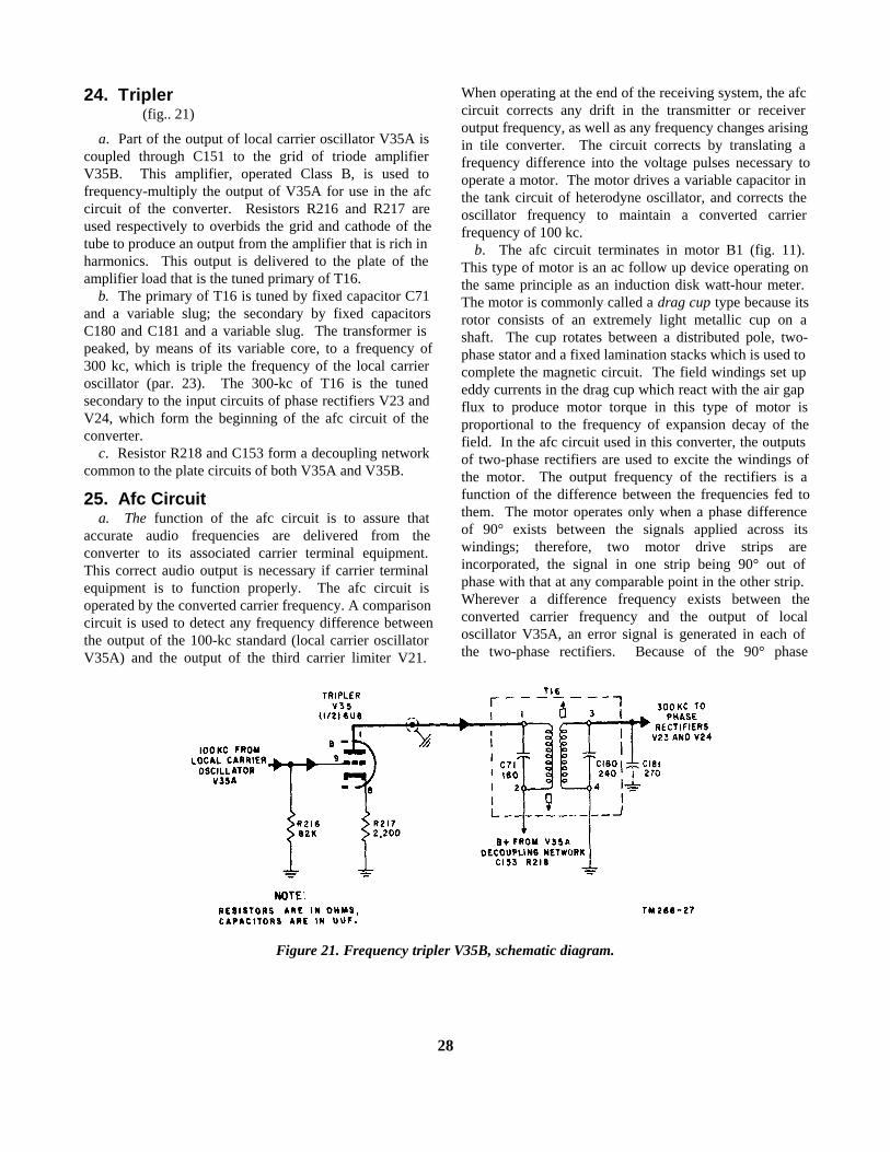
24. Tripler(fig.. 21)
a. Part of the output of local carrier oscillator V35A iscoupled through C151 to the grid of triode amplifierV35B. This amplifier, operated Class B, is used tofrequency-multiply the output of V35A for use in the afccircuit of the converter. Resistors R216 and R217 areused respectively to overbids the grid and cathode of thetube to produce an output from the amplifier that is rich inharmonics. This output is delivered to the plate of theamplifier load that is the tuned primary of T16.
b. The primary of T16 is tuned by fixed capacitor C71and a variable slug; the secondary by fixed capacitorsC180 and C181 and a variable slug. The transformer ispeaked, by means of its variable core, to a frequency of300 kc, which is triple the frequency of the local carrieroscillator (par. 23). The 300-kc of T16 is the tunedsecondary to the input circuits of phase rectifiers V23 andV24, which form the beginning of the afc circuit of theconverter.
c. Resistor R218 and C153 form a decoupling networkcommon to the plate circuits of both V35A and V35B.
25. Afc Circuita. The function of the afc circuit is to assure that
accurate audio frequencies are delivered from theconverter to its associated carrier terminal equipment.This correct audio output is necessary if carrier terminalequipment is to function properly. The afc circuit isoperated by the converted carrier frequency. A comparisoncircuit is used to detect any frequency difference betweenthe output of the 100-kc standard (local carrier oscillatorV35A) and the output of the third carrier limiter V21.
When operating at the end of the receiving system, the afccircuit corrects any drift in the transmitter or receiveroutput frequency, as well as any frequency changes arisingin tile converter. The circuit corrects by translating afrequency difference into the voltage pulses necessary tooperate a motor. The motor drives a variable capacitor inthe tank circuit of heterodyne oscillator, and corrects theoscillator frequency to maintain a converted carrierfrequency of 100 kc.
b. The afc circuit terminates in motor B1 (fig. 11).This type of motor is an ac follow up device operating onthe same principle as an induction disk watt-hour meter.The motor is commonly called a drag cup type because itsrotor consists of an extremely light metallic cup on ashaft. The cup rotates between a distributed pole, two-phase stator and a fixed lamination stacks which is used tocomplete the magnetic circuit. The field windings set upeddy currents in the drag cup which react with the air gapflux to produce motor torque in this type of motor isproportional to the frequency of expansion decay of thefield. In the afc circuit used in this converter, the outputsof two-phase rectifiers are used to excite the windings ofthe motor. The output frequency of the rectifiers is afunction of the difference between the frequencies fed tothem. The motor operates only when a phase differenceof 90° exists between the signals applied across itswindings; therefore, two motor drive strips areincorporated, the signal in one strip being 90° out ofphase with that at any comparable point in the other strip.Wherever a difference frequency exists between theconverted carrier frequency and the output of localoscillator V35A, an error signal is generated in each ofthe two-phase rectifiers. Because of the 90° phase
Figure 21. Frequency tripler V35B, schematic diagram.
28
shift introduced in the phase-shifting network, the errorsignal output of one rectifier is 90° out of phase with theerror signal output of the other rectifier and thus providesthe signal necessary to operate the motor whenever anerror is present in the converted carrier if. The motor ismechanically coupled to capacitor C13, in the grid circuitof oscillator V2, through a reduction gear train ofapproximately 600 to 1 ratio.
26. Phase-shifting Network and PhaseRectifiers
(fig. 22)a. The output of tripler V35B is coupled through
C120 and C122 to be applied in series, effectively, witheach end of the secondary of T14. Also appearing acrossthis tuned circuit is the third harmonic output of afc gateV22. The energy at the secondary terminals is applieddirectly, through coupling capacitors C125 and C128, tothe plates of the dual diode phase rectifier V24, andindirectly, through a phase shifting network, to the platesof phase rectifier V23. Because of the phase-shift effectedin this network the output of V23 is 90° out of phaserelative to that of V24. Little difference in peak outputlevel exists between V23 and V24; however,instantaneously, the level out of one will be passingthrough maximum while the level out of the other ispassing through zero. When the converted carrierfrequency, is higher than the crystal oscillator frequencythe output of one of the phase rectifiers will lead that ofthe other; while, conversely, when the converted carrierfrequency is lower than the crystal oscillator, the lead-lagrelationship of the rectifier outputs will reverse. Thisaction in turn effects the reversal of direction of motortorque and the appropriate adjustment of C13 forcorrection of the mixing oscillator frequency.
b. The phase-shifting action may be demonstrated inthe diagrams of figure 22B. Illustrated as a bridgenetwork, the components R138, C123 C124, and R139have been selected to present virtually equal reactances tothe 300-kc energy appearing at the terminals of thesecondary of T14. Current through leg b-a-e produces avoltage drop across R138, which leads the voltage acrossC123 as shown in the vectorial graph. Since thecapacitive reactance equals the resistance, the totaldifference in phase angle between ER138 and EC123 is
90°. Similarly, the current through the b-d-e legproduces voltage drops that are in phase with the voltagesin b-a-e leg as illustrated. It becomes apparent thereforethat the voltage across d-a is 90° out of phase with thatacross b-e. For simplification of illustrating the phase-shifting function of the network, the source, having animpedance in the order of 125,000 ohms, was consideredto comprise a constant current device, while the loadsacross which EV24 and EV23 appear were considered, ineach case, infinite. Actually, the load circuitry modifiesthe amplitude of EV24 and EV23 to the extent that EV24 isapproximately 3 db lower than EV24 rather than 6 db aswould be indicated by the vectorial diagram.
c. The vectorial diagram and discussion aboveillustrate an instantaneous condition for a single appliedfrequency as it is used to drive the two phase rectifiercircuits. The same shift is felt by all signals that appear atpoints b-e. At the same time, it is obvious that the signalapplied to the plate of V23 through coupling capacitorC126 is 180° out of phase with the signal applied to theother plate of V23 through coupling capacitor C127, andsimilarly the signals coupled through C125 and C128 tothe plates of V24 are 180° out of phase with one another.Therefore, when a single frequency is applied at thesecondary terminals of T14 (as in the case where the afcgate tube is cut off by the squelch circuit) there is acancellation of the output of one diode of the phaserectifier stage by the output of the other diode. Similarly,when the frequency of the local crystal oscillator is thesame as that of the reconditioned carrier, the dc voltagesdeveloped at the junction of load resistors R146 and R147,as well as the junction of R140 and R141, cancel oneanother, and no output is delivered from phase rectifiers tothe afc dc amplifier V25.
d. Whenever a frequency difference exists between thetwo signals that appear at the phase rectifier plates, eachdiode develops an output voltage proportional to theinstantaneous difference between the voltages of the twoapplied signals. Of course, as in any rectifier circuit, eachdiode conducts only when the signal applied to its plate ispositive relative to the cathode potential. The rate ofchange of the output of each phase rectifier is equal to thedifference in frequency existing between the two appliedsignals. Hence an effective beat note is delivered fromeach phase rectifier to the following dc amplifiers. When the
29
TM 266-28
Figure 22. Phase-shifting network and phase rectifiers schematic diagram
30
difference frequency remains constant (that is, when noafc correction is being effected and the converted carrierfrequency is no longer drifting), the output of each phaserectifier is a virtual sine wave or ac voltage. However,under conditions of drift and correction, the outputs maymore accurately be considered pulsating dc voltages.Figure 49 shows the scope pattern that may be observed atthe output of each phase rectifier and C, figure 22indicates the respective output of each during any giveninstant during a theoretical cycle of error signal.
e. The output of V23 is delivered across the cathodeload comprised of R144, R146, C131, R145, R147, andC132. Capacitors C130 and C133 are rf bypass capacitorslocated, respectively, in the plate and output circuits of therectifier.
f. The operation of V24 being the same as that ofV23, corresponding components are provided to performequivalent functions to that described for V23 The outputof V24 is delivered to pin 7 for , of afc ac amplifier V25.Although a slight dissimilarity in level exists between theoutput of V23 and that of V24, error signals of 1 cps(between converter carrier and local carrier oscillatorfrequencies) generate sufficient output from V23 and V24to drive the afc dc amplifier through cutoff or conductcycles, necessary to drive succeeding stages actuating themotor.27. Afc Dc Amplifier
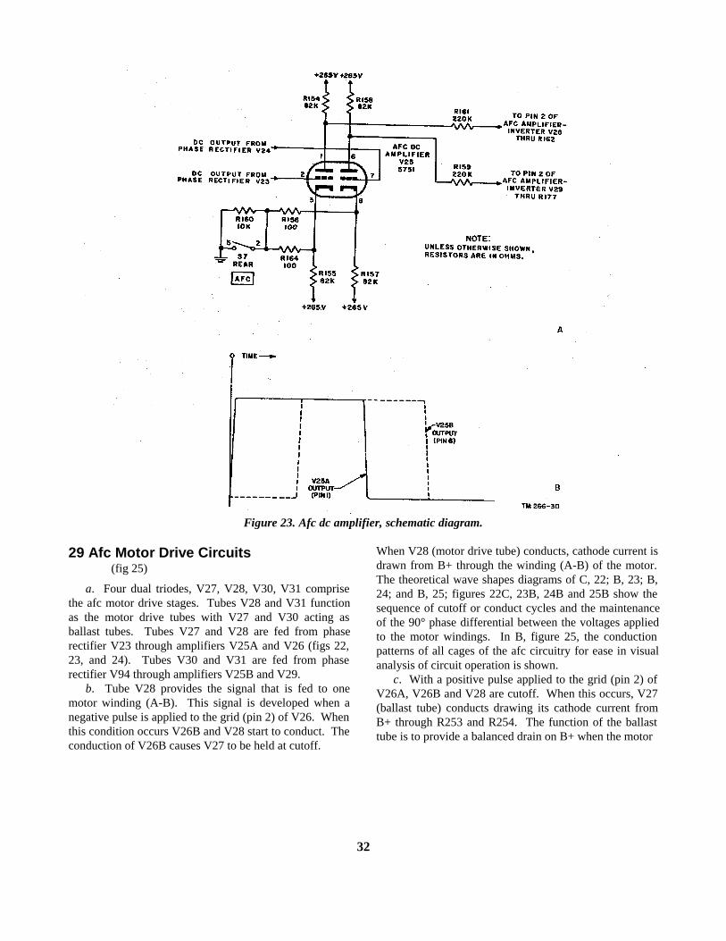
(fig. 23)
a. The output of rectifier V23 is delivered throughgrid-limiting resistor R152 to the grid (pin 2) of V25.The output of V24 is fed through R153 to the grid (pin 7)of V25. Tube V25 functions to amplify the voltage of theoutput of the two rectifiers (while maintaining their phasedifferential) prior to delivery of the signal to the motordrive stages. AFC switch S7 is in the cathode circuit ofV25. When the switch is in the OFF position, cathodes ofV25 are grounded through R160, thus cutting off thetriode sections of the amplifier. In the ON position of S7,bias at the cathode (pin 3) is established through thedividing network formed by R155 and R184 while R157and R156 furnish bias for the cathode (pin 8).
b. Resistors R154 and R158 are the plate-droppingresistors for the stage. The output signal from the plate(pin 1) is developed across divider R161 and R163 (fig.24). The output signal from the plate (pin 6) is developed
across R159. Since the input signals are 90° out of phase(C, fig. 21), this phase relationship is preserved in theoutput from the afc dc amplifier (B, fig. 23). These outputsignals are delivered to amplifiers V26 and V29,respectively.
c. The small difference in voltage that exists at thegrid of each section of the afc dc amplifier (par. 26a)disappears in the cutoff or conduct cycles of the amplifierso that drive to subsequent stages is virtually equal.
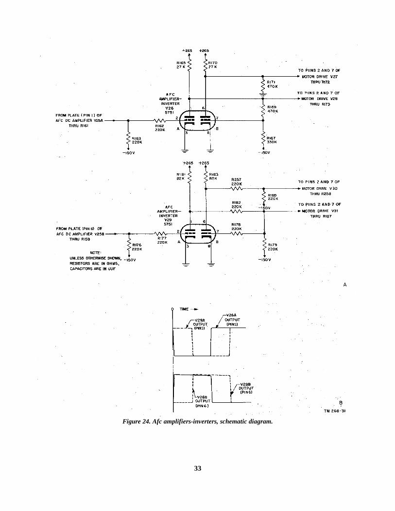
28. Afc Amplifiers-inverters(fig. 24)
a. Two dual triodes, V26 and V29, are used to providethe push-pull output necessary to operate the motor drivestages of the afc circuit. The circuits are nearly identicaland only the operation of V26 will be discussed in detailhere.b. The output from the plate (pin 1) of afc dc amplifierV25 (fig. 23) consists of a dc pulse recurring at thedifference frequency between the output of tripler V35B(fig. 19) and afc gate V22 (fig. 19). The grid (pin 2) ofV26 is biased negative through R163, and the applicationof a signal from the plate (pin 1) of V25 alternately cutsthe tube off, then allows it to conduct, at a rate consistentwith the difference frequency mentioned above.Simultaneously, a similar action takes place in V29A,except that the action of V29A takes place 90° out ofphase with that in V26A. The lag or lead depends on theconverted carrier delivered to the phase rectifiers beinghigher or lower than the standard signal.
c. The output from the plate (pin 1) of V26Adeveloped across the plate load R165 is split. Part of thissignal is delivered through R169 to the grid (pin 7) ofV26. The remainder is fed to the grids of V28. Theoutput from the plate (pin 6) of V26 is biased throughR167 the same as V26A. It operates the same as theinitial section, developing its output signal 180° out ofphase with that produced by V26A. The output of (pin 6)V26 is fed to the grids of V27. Resistor R170 is the plateload resistor for section B of V26.
d. The outputs of the similar stage V29 are deliveredto the grids of V30 and V31. However, they are 90° out ofphase with the outputs of V26, as indicated in the diagramof B, figure 24.
31
Figure 23. Afc dc amplifier, schematic diagram.
29 Afc Motor Drive Circuits(fig 25)
a. Four dual triodes, V27, V28, V30, V31 comprisethe afc motor drive stages. Tubes V28 and V31 functionas the motor drive tubes with V27 and V30 acting asballast tubes. Tubes V27 and V28 are fed from phaserectifier V23 through amplifiers V25A and V26 (figs 22,23, and 24). Tubes V30 and V31 are fed from phaserectifier V94 through amplifiers V25B and V29.
b. Tube V28 provides the signal that is fed to onemotor winding (A-B). This signal is developed when anegative pulse is applied to the grid (pin 2) of V26. Whenthis condition occurs V26B and V28 start to conduct. Theconduction of V26B causes V27 to be held at cutoff.
When V28 (motor drive tube) conducts, cathode current isdrawn from B+ through the winding (A-B) of the motor.The theoretical wave shapes diagrams of C, 22; B, 23; B,24; and B, 25; figures 22C, 23B, 24B and 25B show thesequence of cutoff or conduct cycles and the maintenanceof the 90° phase differential between the voltages appliedto the motor windings. In B, figure 25, the conductionpatterns of all cages of the afc circuitry for ease in visualanalysis of circuit operation is shown.
c. With a positive pulse applied to the grid (pin 2) ofV26A, V26B and V28 are cutoff. When this occurs, V27(ballast tube) conducts drawing its cathode current fromB+ through R253 and R254. The function of the ballasttube is to provide a balanced drain on B+ when the motor
32
Figure 24. Afc amplifiers-inverters, schematic diagram.
33
drive tube is not conducting. Tube V30 and V31 operatein the same manner as V27 and V28. Tube V30 and V31,however, are fed from the signal that originates in phaserectifier V24. This results in the signal applied across themotor winding (C-D) fed from V31 being 90° out of phasewith that delivered from V28. This 90° phase differentialcauses the motor to rotate. The lead and lag relationshipbetween the signals applied across the two windingsdetermines the direction the motor will rotate, and thuswhether it corrects by raising or lowering the frequency ofthe heterodyne oscillator. Capacitors C137 and C138 areprovided to reduce the peak voltages across the motorwinding inductance. Switch S8 is located within afc unitZ1. It connects AFC DRIFT ALARM lamp I 2 andterminals 12 and 13 of TB2 to the 6.3-volt ac supply whenmotor B1 drives capacitor C13 to near the limit of itstravel.30. AGC SELECT Switch and SB AGC
Control(fig. 26)
a. The maintenance of the correct amplitude of theaudio output signal delivered from this converter toterminal equipment is critical. For this reason, controlhas been provided for the agc circuit of the receiver fromthe amplitude of the various parts of the transmitted signalafter they have been separated in the filter circuits of theconverter. This converter is intended for use in thereception of many different kinds of signals (par. 4). Mostof these signals have an undesirable characteristic; theyare unsatisfactory for use in the agc circuit of a receiver.One of the most common types of twin single-sidebandsignals has multiplex teletypewriter intelligence in onesideband and facsimile and a voice order wire in the othersideband. It is desirable to hold the teletypewriterintelligence at a constant amplitude. Since the receiveragc circuit measures the overall input signal to its if.section for the purpose of applying agc voltage, it isevident that the inconstant amplitude of the voice signalin one of the sidebands of the twin single-sideband signalwill cause a strong and short-lined application of receiveragc voltage. This will result in the undesirable effect ofsuppressing and raising the teletypewriter intelligencedirectly with the variations in the amplitude of the voiceintelligence. The problem therefore is one of selection.The agc voltage of the receiver must be controlled by themost critical component in the received signal to provide
for efficient operation by the system. The AGC SELECTswitch provides a means of selecting this critical signalcomponent for the application of agc voltage, after thereceived signal has been separated by the converterfiltering circuits.
b. Switch S10 is a two-section rotary switch. Wafer Aselects the various points in the converter circuit fromwhich signals will be fed to the agc amplifiers andrectifiers. Wafer B merely activates or deactivates the agccircuit of the receiver, depending on whether or not theoperator intends to use the facilities for controlling thereceiver agc from the converter. The switch operates inthe following manner:
(1) In the REC position, contacts 1 and 2 of S10Aconnect the switch input to ground, whilecontacts 7 and 8 of S10A connect the firstcontrol grid (pin 1) of first agc amplifier V36 toground. Contacts 7 and 11 of S10B connect thereceiver agc output from terminal 9 of TB2 tothe receiver through terminal 7 of TB2.
(2) In the CAR position, contacts 3 and 1 of S10Aconnect the 100-kc carrier energy from voltagedivider C94 and C95 to coupling capacitorC154. Contacts 9 and 7 of S10A connect thecoupling capacitor C154 to the first control grid(pin 1) of first agc amplifier V36. Contacts ofS10B connect the converter agc voltage fromAGC TIME switch S11 to the receiver throughterminal 7 of TB2.
(3) In the LSB position, contacts 4 and 1 of S10Aconnect the output of converter upper sidebandfilter FL1 from the secondary of T4 to couplingcapacitor C154 and variable voltage dividerR250. Contacts 10 and 7 of S10A connect thearm of voltage divider R250 to the first controlgrid (pin 1) of first agc amplifier V36.Contacts 11 and 12 of S10B connect theconverter agc voltage from AGC TIME switchS11 to the receiver through terminal 7 of TB2.
(4) In the USB position, contacts 5 and 1 of S10Aconnect the output of lower sideband filter FL3from the secondary of T7 to coupling capacitorC154 and variable voltage divider R250.Contacts 11 and 7 of S10A connect the arm ofvoltage
34
Figure 25. Afc motor drive circuit, schematic diagram.
divider R250 to the first control grid of first agcamplifier V36. Contacts 11 and 12 of S10Bconnect the converter agc voltage from AGCTIME switch S11 to the receiver throughterminal 7 of TB2.
(5) In the TSB position, contacts 6 and 1 of S10Aconnect the converter if. signal from thevoltage dividing network (at the input to carrierif. amplifier V16) to coupling capacitor C154and variable voltage divider R250. Contacts 12and 7 of S10A connect the arm of voltagedivider R250 to the first control grid (pin 1) offirst agc amplifier V36. Contacts 11 and 12 ofS10B connect the converter agc voltage fromAGC TIME switch S11 to the receiver throughterminal 7 of TB2.
c. SB AGC control R250 is a front panel control thatprovides compensation in the agc amplifying circuit forproper operation of the circuit for whatever type ofsideband signal is being received by the converter. Thecontrol is used in the circuit only in the USB LSB, andTSB positions of S10. If a transmitter rated at a givenfixed amount of power output, 1 kilowatt (kw), is used to
transmit all four types of signals at different times duringthe operating schedule, it results in a condition whereby 1kw of power is being used to transmit a pure single-sideband signal, a single sideband signal carrier reduced,a twin single sideband signal carrier reduced, or anordinary double-sideband signal. If the upper sidebandfrequency of all transmitted signals is used to carry amultiplex teletypewriter signal and be comes the mostcritical portion of the signal with respect to its amplitude,it is desirable for this portion of the signal to control thereceiver agc voltage. The various types of signals namedabove have different percentages of the availabletransmitter power used in the transmission of the uppersideband portion of the signal. In the ordinary double-sideband signal, relatively little power is used in thetransmission of the teletype writer intelligence. In thecase of the pure, single-sideband signal, the entire poweroutput (1 kw) of the transmitter is used in the trans-mission of the upper sideband frequencies. The othertypes of signals fall between these two extremes. Theprecise percentage of transmitter power devoted to thetransmittal of teletypewriter intelligence is a function
35
of the degree of carrier suppression. The transmitterradiates 1 kw for the overall signal. It is the differentelements of the signal that are attenuated or raised,depending on the type of signal being transmitted.
d. At the receiving end of the system, the receiver agcsystem sees a signal of the same average amplituderegardless of the type. In the converter, however, thesituation is different. Here, a difference in the percentagesbecomes a difference in absolute values. Therefore, whena pure single-sideband signal is transmitted, the uppersideband frequency, as it appears at the output ofconverter lower sideband filter FL3 (fig. 11), and at theagc circuit, is of very great amplitude, because the entireradiated power of the transmitter is devoted to thetransmission of this single frequency. In the case of adouble-sideband signal, the output of FL3 is very small.Only about 25 percent of 1 kw available power is used totransmit this specific intelligence.
e. If no provision was made for the adjustment of thesignal used to drive the agc circuit, the result would be theapplication of a great amount of agc voltage to thereceiver in the USB, LSB, and TSB positions of S10,when a very great degree of carrier suppression at thetransmitter was used. Very little agc voltage would beapplied to the receiver when the carrier was not beingreduced or when a twin single-sideband signal divided theavailable transmitter power between two sidebands. Theapplication of agc voltage from the converter to thereceiver would bear little relationship to the absolute agcvoltage level required by the receiver to protect it fromover-load and to properly compensate for the increasing orfading of the received signal, but would apply agc voltagedependent on the nature of the received signal and thedegree of carrier suppression used to produce theincoming signal.
f. The function of R250 is to overcome this un-desirable effect. It enables the operator to adjust thevoltage fed to first agc amplifier V36 in accordance withthe type of signal the converter is receiving. Wherefore,for signals that use a relatively high degree of carriersuppression, R250 is adjusted to attenuate the input toV36 by a greater amount. For signals that have a lesserdegree of carrier suppression, R250 is adjusted toattenuate the input to V36 by a lesser amount. Thenormal setting of the SB AGC, control (R250) for the
usual 20-db carrier reduction of the transmitter is 7.5. Donot attempt to use this adjustment as an audio volumecontrol. Audio-output levels are established as outlined inparagraph 68. The adjustment of CARRIER COMPEN-SATOR control R112 (fig. 16) takes care of variations ofcarrier amplitude when the AGC SELECT switch is in theCAR position. A balanced system is thereby achieved toenable the converter to apply agc voltage to the receiver inan amount compatible with the amplitude variationsdisplayed by the received signal.
31. AGC Circuit(fig 27)
a. The output of S10A (par. 30) is delivered to thegrid of a sharp cutoff pentode, V36, which amplifies thesignal and delivers it to a triode amplifier V37A, whichfurther amplifies the signal. The output of V37A is fed tothe grid of the second section of the dual triode, V37B,which has a common grid and plate, thereby acting as arectifier. The dc output of this rectifier is used as acontrol signal, delivered from the converter to operate theagc system of its associated receiver.
b. The output of S10A is fed to the first control grid(pin 1) of V36. The amplifier is biased at the cathode byR219, which is bypassed by C155. The plate is decoupledfrom the high-voltage supply by R221 and C157, thescreen by R220 and C156. Resistor R222 is the plate loadresistor for the stage.
c. The output of V36 is coupled through C158 and isapplied across resistor R225 to the grid of second agcamplifier V37A. Amplifier V37A further amplifies thesignal that is coupled through dc blocking capacitor C160to the plate of V37B. The cathode of V37A is biased byR226, which is bypassed by C161. Inductor L2 is used toprovide the plate load for V37A, while not decreasing theapplied plate potential, to permit greater signal drive toagc rectifier V37B. Resistor R223 and C159 decouplesthe power supply from the plate circuit of V37A.
d. Agc rectifier V37B is a triode, which is connectedas a diode. The cathode of V37B is biased throughresistors R230, R232, R233, R234 and control R231. Thefixed resistors form two dividing networks separated byR231, which is the AGC THRESHOLD adjustment. Oneend of R231 taps off at the junction of R230 and R233,which are series connected between the power supply
36
Figure 27. Agc circuit, schematic diagram.
high-voltage and ground. The other end of the controltaps off the junction of R232 and R234, which are series-connected between the B- power supply and ground. Thecathode of V37B is connected to the arm of the control.As the arm of R231 is varied toward the junction of R230and R933, the cathode of V37B becomes more positive.As the arm is varied toward R232 and R234, the cathodeof V37B becomes more negative. Actually, since R231 isconnected between the B+ and B- supplies in this manner,the cathode of V37B may be varied from -8 volts to +35volts. This design consideration enables the converter tobe adapted for use with receivers that have a variety ofcharacteristics in their agc circuits. Instructions foradjusting R231 are given in paragraph 67. CapacitorC162 is the bypass capacitor for the cathode bias networkof V37B.
e. The dc voltage output of V37B is fed throughisolating resistor R227 and applied across R228, which isthe AGC OUTPUT adjustment. The negative potential atthe arm of R228 varies with the condition of V37B. Themore V37B conducts, the more negative the potential atthe arm of R228 becomes. This change in potential isreflected through isolating resistor R229 to the agc systemof the receiver, thus controlling the application of agcvoltage in the receiver. The function of R229 and the armof R228 is held at effective rf ground potential by C164.Resistor R228 is adjusted to balance the agc voltageoutput with the receiver agc system. Instructions for
adjusting R228 also are given in paragraph 67.f. The AGC TIME switch, S11 is provided to enable
different times of reaction to be selected for operation ofthe agc circuit with various types of signals. The switchselects capacitors which, when placed in the dc outputcircuit of the agc amplifying-rectifying section of theconverter, charge and discharge to slow up the effect ofthe agc circuit. The switch has three positions: SLOW,MED, and FAST. In the FAST position, the output of theagc circuit is connected directly to the receiver and verylittle time delay (caused by C163 and C164) across R227and R228 is introduced. In the MED position, the outputof the agc circuit is connected through terminals 7 and 9of S11 to the ungrounded side of C166. Capacitor C166 isa 1.0-uf capacitor giving the circuit a time constant of 1second. In the SLOW position, the output of the agccircuit is connected through terminals 7 and 8 of S11across C165. This capacitor (12 uf) gives the circuit adelayed reaction of approximately 15 seconds.
32. Monitor Circuit(fig. 27)
a. The MONITOR headset jack (J3) on the front panelof the converter is made available as an aid in varioustuning and testing procedures. The audio output ofeither converter channel A or B may be selected bymeans of the MONITOR
37
switch (S3) on the front panel of the equipment to bedelivered to the monitor output amplifying system. Twoamplifiers are used in the circuit, triode V9A and powerpentode V10 which is operated as a cathode follower.
b. The audio output of channel A, as it appears atterminal l of T5 (fig. 14), is fed to terminal 8 of S3. Theaudio output of channel B, as it appears at terminal 1 ofT8, is delivered to terminal 10 of S3. These are selectedin the A and B positions of the MONITOR switch on thefront panel of the equipment. Terminal 7 of S3 is thewiper contact of the rotary switch through which theselected audio signal; B fed to the grid circuit of V9A. Inthe OFF position of the MONITOR switch, the grid circuitof V9A is connected through terminal 9 of S3 to ground.
c. The selected output of S3 is fed through the voltagedividing network formed by R49 and C50 and appliedacross MONITOR GAIN control R248. The volume ofthe output from MONITOR jack J3 is adjusted byMONITOR GAIN control R248. Cathode bias for V9A isdeveloped across R50 which is bypassed by C51A.Resistor R55 is the plate-dropping resistor for the stage.
d. The output of V9A is coupled through C55 to thefirst control grid (pin 1) of V10. Tube V10 functions as acathode follower output stage. The pentode is connectedas a triodes having a common plate and screen which aredecoupled from the high-voltage power supply by R61 and
C57. The grid resistor, R57, is returned to the lowpotential end of cathode-biasing resistor R58. The loadfor V10 is formed by parallel-connected resistors R59 andR60, in series with R58. The signal developed by V10across this load is coupled through C56 to the MONITORjack on the front panel of the converter where it is madeavailable to a headset or any other suitable audioreproducing device.
33. VU METER Circuit(fig. 29)
a. A meter, calibrated in volume units (vu), ismounted on the front panel of the equipment to provide anindication of the converter audio-output level deliveredfrom channel A or B. A reading of 0 vu on the meterindicates a converter audio-output level of 1 milliwatt intoa 600-ohm line.
b. Through VU SELECT switch (S4) on the controlpanel, the output of channel A or B is applied to vu meteramplifier V9B or the VU METER circuit is turned off. Inthe A position of S4, the audio output of channel A, as itappears at terminal 3 of T5 (fig. 14), fed through contacts8 and 7 of the rotary switch to the grid circuit of V9B. Inthe OFF position, a blank contact (9) is used. In the Bposition, part of the audio output of channel B is taken offterminal 3 of T6 and
Figure 28. Monitor amplifier and output circuit, schematic diagram.
38
Figure 29. VU METER circuit, schematic diagram.
fed through contacts 10 and 7 of S4 to the grid circuit ofV9B. The signal delivered through S4 is coupled throughC53 and applied across the divider formed by R53 andR54 to the grid of triode amplifier V9B. This amplifier isbiased by resistor R52 and control R51, which arebypassed by C51B. VU METER ADJUST control R51varies the bias on the cathode of V9B, thereby calibratingthe meter.
c. The output of V9B is coupled through C54 andapplied across resistor R96 and meter M1. The meter isconnected as a voltmeter with the different multiplyingresistors connected between the plate circuit of V9B andground. Depending on the position of VU RANGE switchS5, either R97, R98, or R99 is placed in the plate circuitof V9B as a shunt to provide the proper meter sensitivity.In the +10DB position of S5, R99 is placed in the circuit.In the 0 DB and -10 DB positions, R98 and R97respectively, are selected as shunts by S5.
34. Power Supply(figs. 30 and 40)
a. General. The power supply converts theprimary ac power source to voltages that satisfy the circuitrequirements of the converter. The converter is operatedfrom primary power sources of 105 through 125 or 210through 250 volts ac, 50 to 60 cps. The converter powersupply converts the primary voltage to 6.3 and 5 volts acfor filament and indicator lamp circuits; +345 volts dc
(unregulated) for the motor drive circuits; +265 volts dc(regulated) for the plate circuits; and -150 volts dc(regulated) for the bias circuits. The dc supplies areregulated to stabilize the operating conditions of theelectron tubes in the converter. Without voltageregulation, electrode voltages would tend to fluctuate inresponse to line voltage variations, as well as changes inload. The two dc supplies use different modes of voltageregulation. The less complex circuit used in the low-current bias supply would not operate satisfactorily in thehigh-current plate supply. Hum and spurious signals onthe power line are isolated from the secondary windings ofthe power transformer by an electrostatic shield groundedthrough the transformer case.
b. Power Input Circuit. The line voltage is impressedacross the primary winding of power transformer T17after passing through PWR IN receptacle J5, VOLTAGESELECT switch S12, and circuit breaker CB1. Thecircuit breaker is located on the front panel and serves asthe converter power switch. Circuit beaker CB1 is athree-wire device, two branches of which containmagnetic tripping elements. Circuit breaker CB1 willopen the primary power circuit when the primary currentexceeds the rating of the magnetic trip in use. When S12is in the 230V position, the entire primary winding of T17is connected to the line through the low-current elementof CB1.
39
Figure 30. Power supply, schematic diagram.TM 266-37
40
the 115V position, S12 connects only one-half of the primarywinding of T17 to the line through the high-current elementof CB1. Overload protection is provided therefore whetherthe converter is operating from a 105- through 125-volt or210- through 250-volt source. The third leg of CB1 does notcontain a magnetic trip but simply connects one side of theincoming line to the No. 1 terminal of the primary of T17.This leg is disconnected automatically when either of theother legs trip, so that power is removed from both sides ofthe transformer primary when a short circuit occurs in theconverter. Additional taps on the primary of T17 provide forline voltages in the 105- through 125-volt and 210- through250-volt ranges. The 115 volts ac is tapped off one-half of theprimary, and is fed to blower motor B2 through J6 and P3.
c. Filament Supply. Transformer T17 has six secondarywindings, four of which are used to supply filament voltagesto the various electron tubes in the converter. The filamentsupply voltages of the various secondaries are distributed inthe following manner:
(1) Terminals 12 and 13 supply 5 volts ac to thefilaments of rectifier tubes V38 and V39.
(2) Terminals 17 and 18 supply 6.3 volts ac to thefilaments of regulator tube V40.
(3) Terminals 19 and 20 supply 6.3 volts ac to thefilaments of dc amplifier V41, motor drivetubes V27 and V28, and the front panelindicator lamp I 3.
(4) Terminals 24 and 26 and center tap terminal 25supply 6.3 volts ac to the filament of rectifiertube V43 and all the filament and indicatorcircuits located in the converter drawerassembly except motor drive tubes V27 andV28.
Note. Tubes V38, V39, V40, V41, V42,and V43 are located on the converter powersupply chassis (fig. 40).
d. 265-Volt Source. The center-tapped power trans-former secondary winding terminating on terminals 14, 15,and 16, supplies high voltage to rectifiers V38 and V39. Thetwo plates of the individual rectifiers are connected together,thus doubling the current rating of each tube. The tubes andthe high-voltage secondary are connected to form a full-waverectifier. The center tap (terminal 15) of the high-voltagesecondary winding is grounded and the pulsating dc is takenfrom one side of the rectifier filament circuit. The high-
frequency components of the pulsating dc are attenuated bythe low-pass filter formed by L4, C167, and C168. Thefiltered dc is fed to the 265-volt regulator stage.
e. 265-Volt Regulator. Regulator V40, dc amplifier V41,and voltage reference tube V42 stabilize the converter platecircuit supply voltage. Regulator V40 functions as a con-trolled resistance connected between the 265-volt source andthe converter circuits making up the power supply load. Thefollowing is a step-by-step analysis of the compensatingaction which tends to make the plate supply voltage immuneto line voltage variations of approximately ±5 percent.
(1) An increase in line voltage results in anincrease in the output of rectifiers V38 andV39.
(2) The voltage across the fond will also increase,until compensated by a rise in, the controlledresistance represented by the plate-cathoderesistance of V40.
(3) A sample of the load voltage is fed to the grid ofdc amplifier V41. The cathode voltage of V41is fixed by a gaseous voltage regulator, voltagereference tube V42.
(4) The increase in voltage at the grid of V41 isamplified and inverted, and appears at the plateas a decrease in positive voltage.
(5) The grids of regulator V40 are connected to theplate of V41. The decrease in voltage at theplate of V41 has the effect of increasing thegrid bias on V40, increasing the plate-cathoderesistance of V40.
(6) The load current through the increased plate-cathode resistance of V40 results in a greatervoltage drop there, and less voltage is deliveredto the load.
(7) The voltage delivered to the converter B+supply is held constant, regardless of whetherthe line voltage should increase or decrease.Current balancing resistors R238 and R239connect the plates (pins 2 and 5) of regulatortube V40 to the filtered output of rectifiers V38and V39 and act as parasitic suppressors. Thecathodes of V40 are connected to the load. Asample of the voltage across the load is takenfrom the movable contact of REGULATORCONTROL R245, a part
41
of voltage divider R244, R245, and R246. Thesample voltage is fed to the grid (pin 1) of dcamplifier V41. The cathode bias of V41 isfixed by the series combination of voltagereference tube V42 and resistor R241. Thescreen voltage of V41 is held fairly constant byresistors R235 and R236. When an increase inline voltage causes a temporary increase involtage across the load, the grid (pin 1) of V41will become more positive. A higher platecurrent flows as a result of this reduced bias.There is a greater drop across R240, the plateload resistor of V41, and the voltage at the platedecreases The grids of V40 (pins 1 and 4) areconnected through parasitic suppressors R242and R243 to the plate of V41. A drop involtage at the plate of V41 results in an increasein grid bias at V40. Thus, the plate-to-cathoderesistance of V40 increases for an increase inline voltage, and the voltage across the load isrestored to its original value. The regulatedoutput voltage will seek an original valuedetermined by the adjustment of R245,regardless of the direction of the line voltagechange. The sample voltage applied to the grid(pin 1) of dc amplifier V41 lags behind theimmediate line voltage change, because of theaction of C171 and C172. If the time delaywere not introduced, the corrective actionwould be regenerative. The combined effect of
C172, and the plate-cathode resistance of V40,is that of a low-pass filter which furthersmoothes the output of the rectifiers, as does theaction of the regulator system.
f. -150-Volt Source and Regulator. Rectifier V43 andvoltage regulator V44 supply the converter with astabilized source of bias voltage. Stabilization of the biassource is necessary to hold bias potentials at optimumvalues that are independent of line-voltage fluctuations.The high voltage secondary winding of T17, terminals 21,22, and 23, supplies high voltage to rectifier V43. Thehigh-voltage winding of V43 are connected to form a full-wave rectifier. The cathode of V43 is grounded, andpulsating dc is taken from the center tap (terminal 22) ofthe high-voltage winding. The pulsating dc is then fed toC169 L5 and C170, and low-pass filter which smoothesout the line frequency components of the rectifier outputvoltage. The negative output voltage is stabilized at 150-volt by the action of gaseous voltage regulator V44 andseries-dropping resistor R237. In a gaseous voltageregulator with a suitable series dropping resistor, theterminal voltage of the regulator will remain constant,with fairly large variations of input voltages. An increaseIn line voltage causes an increase In rectifier outputvoltage. The increase in rectifier output is absorbed as avoltage crop across R237 because of increased currentthrough R237 and V44 which attempts to maintain -150volts across its elements. Regulating action that resultsfrom a decrease in line voltage causes the circuit tooperate in the opposite manner.
42
CHAPTER 3
TROUBLESHOOTING
Note. This chapter contains information for fieldmaintenance. The amount of repair that can be performed byunits having field maintenance responsibility is limited only bythe tools and equipment available and by the skill of therepairman.
35. Troubleshooting Proceduresa. General. The first step in servicing a defective
piece of electronic equipment is to localize the fault.Localization means tracing the fault to the major circuitresponsible for the abnormal operation of the set.Isolation means tracing the fault to the defective partresponsible for the abnormal condition. Some faults suchas burned-out resistors or capacitors and shortedtransformers often can be located by sight, smell, andhearing. The majority of faults, however, must be isolatedby checking voltages and resistance.
b. Procedure. The tests listed below aid in isolatingthe sources of trouble. To be effective, the procedureshould be followed in the order given. Servicing shouldcause no further damage to the equipment. First, troubleshould be localized to a single stage or circuit; then thetrouble may be isolated within that stage or circuit byvisual inspection, voltage and resistance measurementsand signal substitution.
(1) Visual inspection. The purpose of visualinspection is to locate any visible trouble suchas loose, broken, or charred parts. Through thisinspection alone, the repairman frequently maydiscover the trouble, or determine the stage inwhich the trouble exists. This inspection isvaluable in avoiding additional damage to theequipment which might occur throughimproper servicing methods and in forestallingfuture failures.
(2) Resistance measurements. These measure-ments (par. 42) prevent further damage to theequipment from possible short-circuits. Thistest gives an indication of the condition of thefilter circuits; therefore, its function is morethan preventive.
(3) Troubleshooting chart. The symptoms listed inthis chart (par. 41) will aid greatly in localizingtrouble.
(4) Operational test. The operational test (par. 40)is important because it frequently indicates thegeneral location of trouble. In many instances,the information gained will determine the exactnature of the fault. To use this informationfully, all symptoms must be interpreted inrelation to one another.
(5) Signal substitution and signal tracing. Theprincipal advantage of the signal substitutionand signal tracing method is that it usuallyenables the repairman to localize a troubleaccurately and quickly to a given stage whenthe general location of the trouble is notimmediately evident from other tests.
(6) Intermittent troubles. In all these tests, thepossibility of intermittents should not beoverlooked. If present, this type of trouble oftenmay be made to appear by tapping or jarringthe set. It is possible that the trouble is not inthe converter, but in the installation (cabling toreceivers, power cable, or carrier terminalequipment connections) or the trouble may becaused by external conditions. In this event,test the installation, if possible.
36. Troubleshooting DataThe material supplied in this manual will help in the
rapid location of faults. Consult the following troubleshooting data.
Fig. Par. Description
44 ---- Converter removal and disassembly.46 ---- Afc unit, exploded view.49 ---- Afc circuit oscilloscope test points.50 ---- Alinement and adjustment points on converter
43
36. Troubleshooting Data-Continued
Fig. Par. Description
62 ------- MIL-STD resistor color code.63 ------- MIL-STD capacitor color code.64 ------- Tube socket voltage and resistance data chart.65 ------- Resistor and capacitor board voltage and resistance
chart.66 ------- B+ and B- voltage distribution diagram.67 ------- Converter, schematic diagram.68 ------- Converter, Wiring diagram.
37 Test Equipment required for field maintenance.39 Checking B+ and B-for shorts.30 Operational test.41 Troubleshooting chart.42 Dc resistances of transformers, coils, and filters.43 Signal substitution and signal tracing notes.45 Replacement of parts.46 Disassembly and reassembly of afc unit Z147 Relay adjustments.48 Troubleshooting afc circuit.
50-68 Alinement
37. Test Equipment Required for FieldMaintenance
The test equipment recommended for trouble-shootingSingle Sideband Converter CV-157/URR is listed below.The manuals associated with the test equipment also arelisted.
Test equipment Technical manual
Tool Equipment TE-113-------------------------- ----------------------------Tool Equipment TE-114-------------------------- ----------------------------Multimeter TS-352B/U---------------------------- TM 11-5527ASignal Generator AN/URM-25------------------ TM 11-5551Electronic Multimeter ME-6A/U---------------- TM 11-5549Electron Tube Test Set TV-2/U----------------- TM 11-2661Electron Tube Test Set TV-7/U----------------- TM 11-5083Frequency Meter FR-67/U----------------------- TM 11-2698Audio Oscillator TS-382A/U-------------------- TM 11-2684ASound Analyzer TS- 615/U---------------------- TM 11-5032Oscilloscope OS-8A/U---------------------------- TM 11-1214Variable Transformer CN-16A/U-------------- ----------------------------
38. General Precautions(figs. 31-36)
Whenever the converter is serviced, observe thefollowing precautions carefully:
a. When removing the drawer assembly from the base
assembly (fig. 44), be careful not to place a strain on theinterconnecting cabling.
b. Be careful when the drawer assembly is extended;dangerous voltages are exposed.
c. Careless replacement of parts often makes newfaults inevitable. Note the following points:
(1) Before a part is unsoldered, note the position ofthe leads (figs. 32-35). If the part, such as atransformer, has a number of connections, tageach of the leads to it.
(2) Be careful not to damage other leads by pullingor pushing them out of the way.
(3) Do not allow drops of solder to fall into the set;they may cause short circuits.
(4) A carelessly soldered connection may create anew fault. It is important to make well-soldered joints because a poorly soldered jointis one of the most difficult faults to find.
39. Checking B+ and B- for Shortsa. General. Trouble within the converter may be
detected by checking the resistance of the high voltagecircuits before applying power to the equipment,preventing damage to the power supply. Make thefollowing checks before attempting to put the converter inoperation. The front panel power switch must be in theOFF position before any of these measurements areattempted. The setting of other controls and adjustmentsis unimportant.
b. Unregulated B+ Test. The measured resistancebetween unregulated B+ and ground should be 130K. Aconvenient test point is the high potential terminal ofR238 (figs. 30 and 41). The high potential end of R238 isnearest the bottom of the power supply chassis. Theunregulated part of the +265-volt supply is isolated fromthe load by the plate-cathode resistance of regulator V40.The plate-cathode resistance of V40 approaches infinitywhen the converter is turned off. Thus, resistancemeasurements at this point will only show up defects incomponents at the input to regulator V40.
c. Regulated B+ Test. The value of the resistancemeasured between regulated B + and ground should be23K. A convenient test point is the high potentialterminal of C172, mounted in the converter, baseassembly (fig. 38). The high potential terminal of C172may be identified by the two red wires. This resistancemeasurement tends to reveal defects in the componentsconnected to the output of regulator V40 but will notreveal
44
defects in components connected the input side of V40.d. Regulated B- Test. The measured resistance
between regulated B-test point and ground should be 25K.The terminal of C170 to which the two violet-white wiresare connected is a convenient test point. The capacitor ismounted in the base assembly and is located near the rearleft corner of the assembly (fig. 38).
e. Significance of Resistance Measurements. If any ofthe above resistance values drop to a few hundred ohms orless, a short in the wiring, rectifier tubes, or filtercapacitors may be suspected. Any other change in resis-tance values must be analyzed critically by referring to theB+ and B-voltage distribution schematic (fig. 66). Leakyor shorted capacitors, interelectrode electron tube shorts,or wiring or resistor defects could cause deviations fromthe normal resistance values. Many component defectswill not show up as a change in resistance value at the testpoint because of the magnitude of the isolation or loadresistors in the circuit. Occasionally, circuits that shortwith high voltage applied will not appear shorted to thelow voltage of an ohmmeter. Other shorts occur onlywhen the tubes are hot and can only be determined byother tests.
40. Operational Testa. If the converter is connected with its associated
components for normal operation, refer to the set manualto operate the equipment.
b. If the converter is being checked independently of thesystem, perform the following procedures to makeit ready for operation:
(1) To simulate an input signal, connect SignalGenerator AN/URM-25 at IF. INPUT jack J1.Set the generator to deliver 455-kc output at10,000 microvolts (uv) modulated 30 percent
with a 1,000-cps note. This input will simulatea double-sideband signal input to the converter,which is satisfactory for the operational testingof the converter.
(2) To simulate an output load, connect four 300-ohm resistors across the terminals of TB1. Onebetween terminals 1 and 2, one betweenterminals 2 and 3, one between terminals 4 and5, and one between terminals 5 and 6.
c. Tracking the afc circuit may be checked by slowlyvarying the converter VERNIER control while monitoringeither channel A or B and observing the DRIFT INDI-CATOR control. The pitch of the tone in the monitoredchannel should remain the same and the DRIFTINDICATOR should track, showing the same deviationfrequency as the VERNIER control is varied over itsrange.
d. Connect the headset (or other auditor monitor) tothe channel A output and then to the channel B output onTB1 (terminals 1 and 3 for A; 4 and 6 for B). A strongoutput indicates each channel is functioning.
41. Troubleshooting ChartThe following chart is supplied as an aid in locating
trouble in the converter. The chart lists the symptoms thatthe repairman observes while making a few simple testswith the equipment connected as instructed in paragraph40. The chart indicates how to localize trouble quickly tothe input, sideband amplifiers, carrier amplifiers, demod-ulators, audio amplifiers, limiters, agc, afc, or powersupply sections of the converter. Once the trouble hasbeen localized to a stage or circuit, a tube check andvoltage and resistance measure meets of this stage orcircuit ordinarily should be
sufficient to isolate the defective part. However,sometimes it may be necessary to run the signal tracingcheck (par. 43). Normal voltage and resistance measure-ments are given in figures 64 and 65. Instructions for
connecting the converter for use with this chart are givenin paragraph 40. Signal substitution and tracingprocedures are described in paragraph 44.
Item Symptom Probable trouble Correction1 CB1, converter power switch throws
automatically to OFF position.Short circuit in converter................ Disconnect converter from power
source.Check B+, B- and filament supplies
for shorts (par. 39).Check between terminals of P3 for a
short.Trace short circuit following voltage
and resistance data charts (fig. 64and 65).
2 Pilot lamp I 3 fails to light when CB1 is in ONposition.
I 3 burned out. VOLTAGESELECT switch S12 (fig. 5) inwrong position and/or TB3 TB4tapped improperly.
Check I 3. Replace.Check S12 and power transformerT17 primary taps (on TB3 and TB4).
Failure in T17 (fig. 30)................... Check T17, voltages and resistance.3 No audio output at MONITOR jack J3 when VU
METER indicates audio signal present.MONITOR GAIN and MONITORswitches improperly positioned.
Check setting of these controls.
Failure in monitor circuits.............. Signal trace audio through S3 andthrough monitor amplifiers V9 andV10 by using headset isolated by.1-microfarad (uf) capacitor.
Check S3 (fig. 37).Use tube socket voltage and
resistance chart to check circuits ofV9 and V10 (figs. 64 and 65).
4 No indication on VU METER, no audiblesignal at MONITOR jack for eitherchannel A or B, but CARRIER LEVELmeter indicates.
Converter improperly tuned..........Failure in V9................................
Retune converter.Use voltage and resistance charts to check circuits of
V9 and V10 (fig. 64 and 65). Replace.
Failure in local carrier oscillatorV35
Throw CARRIER SELECT switch S6 to RC position.If monitoring facilities indicate signal is nowpresent, use voltage and resistance charts to checkcircuits of V35. Replace.
Failure in S6................................ Make continuity check of S6. Repair when possible.Replace.
Failure in S1................................ Make continuity check of S1. Repair when possible.Replace.
5 Sideband tone monitors satisfactorily inappropriate channels on either RC orLC position of CARRIER SELECTswitch S6. CARRIER LEVEL meterdoes not indicate. SQUELCH ALARMlamp lights and remains lighted as soonas SQUELCH switch is turned to theON position.
Failure in squelch voltage rectifierV32.
Failure in CARRIER LEVELmeter M2 or its circuits.
Use voltage and resistance charts to check circuit ofV32. Replace.
Check M2 and its circuits. Repair or replace.
6 No indication on VU METER whensignals are audible at MONITOR jack.
VU RANGE or VU SELECTswitch improperly positioned.
Check setting of these controls.
Failure in VU METER amplifyingcircuit.
Use voltage and resistance charts to check circuit ofV9 (fig. 64). Check S4 and S5 (fig. 37).
7 No indication on VU METER. Noaudible signal at MONITOR jack inone channel (either A or B), but whenSB SELECT switch is turned tointerchange channels (VU SELECT andMONITOR switches also appropriatelychanged), VU METER deflects andsignal becomes audible in new channel.CARRIER LEVEL meter indicatingsatisfactorily.
If channel A fails but channel Boperates properly, failure is inchannel A between S1 and T5(fig. 67).
If channel B does not operate butchannel A operates properly,failure is in channel B betweenS1 and T6 (fig. 67).
Use voltage and resistance charts to check V5, V6,V7, and V8. Run continuity checks on FL2, FL6,and S2B. Replace if necessary.
Use voltage and resistance charts to check V12, V13,V14, and V15. Run continuity checks on FL4,FL7, and S2A. Replace if necessary.
8 Lower sideband frequencies do notmonitor or give VU METER indicationin either channel A or B. Uppersideband frequencies audible whenmonitored in either channel and givesatisfactory indications on VU METERin both channels. CARRIER LEVELmeter indicates satisfactorily.
Upper sideband frequencies do notmonitor or give VU METER indicationin either channel A or B. Lowersideband frequencies audible whenmonitored in either channel and givesatisfactory indication on VU METERin both channels. CARRIER LEVELmeter indicates satisfactorily.
Failure in circuit of V4.................
Failure in circuit of V11...............
Failure in S1................................
Use voltage and resistance data charts and check V4.Trace signal through these elements. Also checkcontinuity of T3, FL1, and T4.
Use voltage and resistance charts and check V11.Also check continuity of T6, FL3, and T7.
9 Sideband intelligence may bemonitored in LC position ofCARRIER SELECT switch, but notin RC position. AFC INDICATORdoes not move when AFC switch isin ON position. CARRIER LEVELmeter indicates satisfactorily andSQUELCH ALARM does not lightwhen SQUELCH switch is in ONposition.
Failure in circuit of V19, V20, orV21.
Use voltage and resistance chartsto check circuits of limiter strip.Check tubes V19, V20, and V21.
10 Sideband intelligence may bemonitored in LC position ofCARRIER SELECT switch, but notin RC position. AFC INDICATORshows satisfactory tracking of afccircuit. CARRIER LEVEL meterindicates satisfactorily. SQUELCHALARM does not light whenSQUELCH switch is in ONposition.
Failure in CARRIER SELECT switch,S6.
Make continuity check of S6.Repair or replace.
11 Sideband intelligence may bemonitored in LC position ofCARRIER SELECT switch, but notin RC position of CARRIERSELECT switch. CARRIERLEVEL meter shows no reading.SQUELCH ALARM lamp lightsimmediately when SQUELCHswitch is turned to ON. AFCINDICATOR shows no tracking ofafc circuit.
Failure in circuit of V16, V17, orV18.
Use voltage and resistance datacharts to check circuits of V16,V17, and V18.
12 No intelligence in either channelindicated by monitoring facilities inboth LC and RC positions ofCARRIER SELECT switch. Noreading on CARRIER LEVELmeter. SQUELCH ALARM lightsand remains lighted whenSQUELCH switch is turned ON.
Failure in mixer, heterodyneoscillator, or first if amplifier.
Use voltage and resistance datacharts to check circuits of V1,V2, and V3.
13 SQUELCH ALARM lights andstays lighted after SQUELCHswitch is turned ON, even thoughCARRIER LEVEL meter indicatessatisfactory input to limiter strip.AFC INDICATOR does not trackfrequency drifts
Squelch adjustments poorly made.......
Failure in relay K1..............................
Failure in V33 or V34.........................
Failure in circuit of V19, V20, orV21.
Check squelch circuit (par. 76).
Check K1 (par. 47).Use voltage and resistance datacharts to check circuits of V33and V34.Use voltage and resistance datacharts to check circuits of V19,V20, and V21.
14 SQUELCH ALARM does not light,even when signal generator isdisconnected from converter IF.INPUT receptacle.
Failure in I 1.......................................Squelch adjustments poorly made.......
Failure in V32, V33, or V34...............
Failure in relay K1..............................Failure in S9.......................................
Check I 1.Check adjustments in squelchcircuit (par. 64).Use voltage and resistance datacharts to check circuits of V32,V33, and V34.Check K1.Make continuity check of S9.
15 AFC INDICATOR does not move whenconverter VERNIER control is movedslowly. SQUELCH ALARM lamplights, when VERNIER control hasbeen moved slightly. Monitoredintelligence changes in pitch (in LCposition of CARRIER SELECTswitch) as VERNIER control ismoved.
P2, J4 (fig. 37) disconnected.................Failure in afc gate.................................
Failure in tripler V35B..........................
Failure in afc circuit..............................
Check P2 and J4.Use voltage and resistance charts to
check output circuits of V22.Use voltage and resistance charts to
check circuit of V35B.Refer to paragraph 48.
16 AFC INDICATOR shows erratictracking. Converter continuallydetuned by afc circuit. SQUELCHswitch ON.
Converter or receiver improperly tuned.
Poor signal being received and squelchcircuit has failed.
Check tuning instructions for type ofoperation being used.
If possible, check quality of receivedsignal. Check output of receiver toconverter. If signal input toconverter is present, run squelchcircuit alinement procedure (par. 64)as check, (follow procedure, butmake no adjustments. This willlocalize trouble or improperly setthreshold adjustment.)
17 AFC INDICATOR runs continuallywhen converter input signal has notdrifted appreciably.
Failure in afc circuit Refer to paragraph 48.
18 AFC DRIFT ALARM lamp does notlight when AFC INDICATORreaches +2 KC or -2 KC calibrationmark.
Failure in S8 or I 2 Check switch (located in Z1) and lamp.
19 Unsatisfactory audio-output level fromconverter in either channel A or B(but not both) when A-VC and B-VCcontrols properly set. CARRIERLEVEL meter registers. AFCoperative.
Failure in sideband amplifier,demodulator or audio-output stagesof affected channel.
Use voltage and resistance charts tocheck circuits of V5, V6, V7, and V8if failure in channel A. Check V12,V13, V14, and V15 if failure inchannel B.
20 Overly distorted audio output fromconverter.
CHAN. A BIAS ADJUST or CHAN. BBIAS ADJUST control improperlyadjusted, or other amplifier defects.
Use voltage and resistance checks ofamplifiers involved, particularly gridbiases (par. 66).
21 No agc voltage applied from converterto receiver (for any position of AGCSELECT switch).
5-6 ............................. 21.T14.................... 1-2 ............................. 30.T16.................... 3-4 ............................. 16.T17.................... 1-2 ............................. Less than 1.
1-6 ............................. Less than 1.1-7 ............................. 1.6.1-11 ........................... 2.2.19-20 ......................... Less than 1.12-13 ......................... 0.17-18 ......................... 0.14-15 ......................... 26.15-16 ......................... 26.24-25 ......................... 0.25-26 ......................... 0.21-22 ......................... 70.22-23 ......................... 70.
43. Signal Substitution and SignalTracing Notes
a. General. It is often easier to localize a faulty stageby tracing a signal throughout the equipment by using asignal generator and an electronic volt-meter. Once thefaulty stage has been located, it is easy to find thecomponent that caused the failure. The charts belowindicate voltage values ( 10 percent) when SignalGenerator AN/URM-25 and Electronic Multimeter ME-6A/U are used for tracing signals through the converterstages. The measurements should be taken whilesimultaneously using the converter schematic diagram(fig. 67) to find whether a deviation is caused by failure inthe stage at which measurements are being made, orwhether the failure lies ahead of that stage. Make themeasurements in the order in which the charts list them.Where rf voltages are indicated, use the diode probe of theelectronic multimeter. Where ac or dc voltages areindicated, do not use the probe.
b. Preparatory Procedure. Before attempting any ofthese measurements, INPUT GAIN control R2 must beestablished at a standard setting. To establish thisstandard, proceed as follows:
(1) Connect Signal Generator AN/URM-25 at IFINPUT jack J1. Set the generator to deliver452-kc unmodulated output at 10,000 uv.
(2) Turn the converter on, and set the VERNIERAND DRIFT INDICATOR controls at O, KC,and the CARRIER SELECT switch at LC. Noother converter controls influence thismeasurement.
(3) Connect Electronic Multimeter ME-6A/U atterminal 3 of T4.
(4) Adjust the INPUT GAIN control for a readingof .1 volt rf on the multimeter.
(5) The INPUT GAIN control is now at thestandard setting used to obtain themeasurements below.
c. Carrier and Agc Section Measurements.(1) Set Signal Generator AN/URM-25 to deliver
455-kc unmodulated output at 1,000 uv.Connect the generator at IF INPUT jack J1.
(2) Set the converter front panel controls asfollows:
58
Control SettingAFC................................ ...................ON.AGC SELECT................................ ....CAR.CARRIER SELECT ...........................RC.DRIFT INDICATOR..........................O. KC.VERNIER................................ ..........To center signal in carrier
stages as indicated byreading on the CARRIERLEVEL meter.
CARRIER COMPENSATOR. To produce midscale readingon CARRIER level meter.
SQUELCH................................ .........ON.Note. It is impossible to obtain correct
tracking of the afc circuit, turn the AFC controlto OFF and proceed with the measurements.These symptoms indicate failure in the converterand it is probable that signal tracing procedurewill reveal the faulty stage.
(3) Make all the following measurements to groundwith rf or dc probe of Electronic MultimeterME-6A/U.
(4) To check the clipping action of the carrierlimiter section (V19 (V20, AND V21) andV21), increase the output of the signalgenerator to 10,000 uv. Reset the CARRIERCOMPENSATOR to provide midscalereading on the CARRIER LEVEL meter,and repeat the measurement at terminal 3 ofT13. It still should measure 12 volts. Tocheck the amplifying action of the limiterstrips turn the SQUELCH control to OFFand reduce the output of the signal generatorto 110 uv. Readjust the CARRIER LEVELCOMPENSATOR to restore the midscalereading on the CARRIER LEVEL meter.The rf reading at Terminal 3 of T13 shouldnot be reduced more than 2 db (9.3 volts).
Filter (FL5).............................. Output..... ...... ... Junction of R110,R111.
.006
First carrier amplifier (V17) ..... Output..... V18 1 ......................... 37Second carrier amplifier(V18). . Output..... V19 2 ......................... 49 If measurements to this point are correct
but CARRIER LEVEL meter does notindicate properly, failure is in V32 ormeter.
First carrier limiter (V19) ......... Output..... V20 2 ......................... 3.0Second carrier limiter (V20)..... Output..... V21 2 ......................... 9.7 If measurements to this point are correct
and SQUELCH ALARM remainslighted, failure is in squelch circuit.
Output..... ...... ... Term. 3 of T14 1.8Local carrier oscillator..............V35
............... ...... ... Term. 3 of T15 6.2 If all measurements to this point arecorrect and AFC INDICATOR stillwill not track, failure is in afc circuits.
d. Converter Upper Sideband, Channel A, and AgcMeasurements(1) Connect the rf output of Signal Generator AN/URM-
25 to IF. INPUT receptacle J1. Set the generator todeliver an unmodulated 452-kc output at 10,000 uvThe 452-kc signal will beat to fall in the converterupper sideband and will produce an audio tone at thedemodulator.
(2) Set the converter front panel controls as follows:
Control SettingSB SELECT................ A-LSB, B-USB.AGC SELECT............. LSB.CARRIER SELECT .... LC.SB AGC...................... 7.5.AGC TIME ................. MIN.
Control SettingVU SELECT A.VU RANGE 0 DB.A-VC +10 db reading on VU
METER.AFC OFF.SQUELCH OFF.VERNIER O KC.DRIFT INDICATOR O KC.
Note. If it is impossible to obtain a +10 dbreading on the VU METER by adjusting the A-VCcontrol, proceed with the measurements to discoverthe failure causing this symptom (par. 41).
(3) Make the following measurements to groundwith an rf, ac, or dc probe of ElectronicMultimeter ME-6A/U.
Make measurement atStage Voltage Tube Pin Other Reading (volts)
Audio output (V15)................................ ..... ............... ........... ........ Term. 4 of TB1 ............ 1.2 ac.Term. 6 of TB1 ............ 1.2 ac.
(3) Connect Signal Generator AN/URM-25 to IF.INPUT receptacle J1. Set the generator todeliver a 456-kc unmodulated output at 10,000uv. This 456-kc signal will beat to fall in theconverter lower sideband and will produce anaudio tone after demodulation
(4) Set the converter controls as follows:
Control SettingSB SELECT......................... LSB-B, USB-A.AGC SELECT...................... USBCARRIER SELECT ............. LC.VERNIER............................ O KC.DRIFT INDICATOR............ O KC
Control SettingVU SELECT........................ B.VU RANGE......................... + 10 DBB-VC................................ ... 0 db reading on VU METER.AFC................................ ..... OFF.SQUELCH........................... OFF.
(5) Make the following measurements to groundwith Electronic Multimeter ME-6A/U.
(6) Restore the original settings of the INPUTGAIN A-VC and B-VC controls at theconclusion of signal tracing test.
Make measurement at ReadingStage Voltage Tube Pin Other (volts)
Output .... ........... ......... Term. 3 of T7 ........... .1
.
61
CHAPTER 4REPAIRS
44. Removal and Disassembly ofConverter for Servicing.
a. Figure 44 shows the steps necessary for removal ofthe converter from the rack and mechanical disassemblyfor servicing. Normally, it is not necessary to separate thedrawer and base assemblies to reach the bottom of theoscillator section however, release the catches on thedrawer slides and separate the base and drawerassemblies.
Caution: The cables that connect the drawer and baseassemblies are short. Be careful not to break these cableswhen removing the drawer from the base.
b. The top and the bottom of the oscillator section(containing local carrier oscillator V35 and crystal ovenHR1, figure 31) are shielded. Take off the shields byremoving the screws that hold them in place.
45. Replacement of Partsa. General. Most of the converter components can be
easily reached and replaced if found to be faulty. Beforeattempting the replacement of any part, be sure the powerswitch is in the OFF position. The premature failure of areplacement part or an associated component can beminimized if the following precautions are observed:
(1) Be careful when replacing parts that requireseveral electrical connections. As the wires onthe part are removed, tag them to facilitateproper connection when the replacement part isinstalled.
(2) When leads of other converter componentsinterfere with part replacement, be careful whenmoving the interfering leads out of the way.The interfering leads, as well as thecomponents, may be damaged.
(3) Soldering should be done carefully. Acarelessly soldered connection may create a
new fault, which will be difficult to find. Freedrops of solder left in the equipment are apotential source of trouble.
(4) A replacement part should be installed in thesame position as the original. Give particularattention to proper grounding, when replacing apart. Use the same ground connection as in theoriginal wiring.
b. Electron Tube Replacement. Most of the tubes arereadily accessible by removing the converter dust cover(fig. 31). Avoid forcing any of the miniature tubes duringremoval or replacement operations. Careless handling ofthese tubes may result in bending the base pins. Localcarrier oscillator V35 can only be replaced after firstremoving the oscillator shield located on the rear of theconverter chassis. Tubes V38 through V44 are located onthe base-mounted power supply chassis (fig. 40). Specialprecautions should be taken when removing V38, V39, orV40, as they are held in place by base clamps. Inaddition, V38 and V39 have clamps about the glassenvelopes. These clamps must be loosened before thetubes can be removed.
c. Afc Unit Removal. Afc unit Z1 must be removedfrom the converter if the unit is to be disassembled.Remove the DRIFT INDICATOR knob. Disconnect P2 byrotating the locking ring 90° and withdrawing the plug.Disconnect P1 by unscrewing the locking sleeve, thuswithdrawing the plug. The afc unit finally may beremoved from the converter after the four machine screwsthat attach the unit to the front panel are removed.
d. Power Supply chassis Removal. Severalcomponents associated with the power supply circuits arelocated on the underside of the base mounted powersupply chassis must be removed and inverted to reachthese components. Remove the six machine screws thathold the chassis to the converter base, and the chassis maybe removed from the base assembly.
62
There is a considerable amount of slack in the cable thatconnects the power supply chassis and the converter baseassembly. The power supply chassis must be invertedcarefully to avoid twisting the interconnecting cableexcessively.
e. Carrier Oscillator Section. To gain access to thebottom of the carrier oscillator section, follow theprocedure shown in figure 44.
Note. In replacing either the bottom cover or the top shield ofthe oscillator section, use -inch (max length) screws to avoidestablishing undesired grounds between oscillator subchassisand rf chassis.
f. Front Panel Removal. Remove the front panelcarefully; panel-mounted components and associatedwiring may be damaged. Particularly, the extension shaftswhich must be re-fitted through the panel on reassemblyshould be carefully handled to avoid striking componentsand wiring. Follow the steps below to remove the frontpanel; the afc unit, indicator lights, and meters remain onthe panel.
(1) Remove all knobs except that of the DRIFTINDICATOR.
(2) Disconnect PI and P2 from the afc unit (fig.34).
(3) Disassemble the nut, dial, and washer from theVERNIER shaft.
(4) Remove the nuts and washers from MONITORjack J3 and all other controls.
(5) Unsolder the leads to indicators I 1 and I 2, andmeters M1 and M2.
(6) Remove the mounting screws that hold theVERNIER capacitor.
(7) Remove the 10 screws and washers that holdthe front panel to the rf chassis.
g. Access to Components Mounted Beneath TerminalBoards. To repair or replace some components, terminalboards or other components must be removed.Components that are difficult to reach and the preferredmethod to reach them are listed in the chart below.
To repair or replace these components Remove these parts How
T11 (or any associated with its terminals),C101, C84, and C85 (fig. 32).
Shield (left, fig. 32) ............................... Remove two nuts that hold mountingstuds.
Pull shield straight upward.Any on the shield side of TB14 (fig. 65). Adjacent shield (fig. 34) ........................ Remove CARRIER COMPENSATOR
control shaft by loosening set screw oncoupler.
Remove two nuts that hold mountingstuds.
Slide shield straight upward, exposingcomponents.
FL2, TB28, and any associated withsockets for V5, V12, and V6 (fig. 65).
FL6 (fig. 35)................................ .......... Remove two nuts that hold mountingstuds; unsolder two leads.
Coaxial cables ................................ ....... Push upward, singly, out of slot in whichthey lie.
SB SELECT switch shaft ....................... Loosen setscrew on coupler.Any associated with socket for V13 FL (fig. 35)................................ ............ Remove two nuts that hold mounting
studs; unsolder two leads.SB SELECT switch shaft ....................... Loosen set screw on coupler.
AGC SELECT switch S10 (fig. 35) Front panel Refer to f above.CHAN B BIAS ADJUST control R86 (fig.42).
Cable clamp on chassis adjacent to R86(fig. 32).
Remove two mounting screws and nuts.
SB AGC control R250......................... Front panel ................................ ............ Refer to f above. Unsoldering leads tofront panel components is not necessarysince wire slack permits panel to bepulled away from rf chassis enough toallow access to this control.
TB26 or any components on panel side(fig. 65).
Front panel ................................ ............ Refer to f above.
CARRIER SELECT switch shaft (fig. 35). Loosen setscrew on coupler.Bracket between front panel and TB26. Remove two mounting screws and washers
to permit bracket to be moved towardfront panel, enough to allow access tocomponents.
63
To repair or replace these components Remove these parts HowFL4 (fig. 31) ................................ .......... C74 (fig. 33) .............. Remove mounting hardware only; wire slack permits
sufficient movement of capacitor for access to four nutsand washers that secure the filter.
T17 (fig. 39) ................................ .......... Panel stiffener ............ Remove six screws that hold L-bracket stiffener to frontpanel.
CB1 ........................... Disassemble circuit breaker from front panel. Wires need notbe unsoldered.
L5 .............................. Remove nuts and washers that hold mounting studs.Move components about ½-inch to leave clearance for
removal of T17. Remove four nuts and washers that holdmounting studs on transformer.
L4 (fig. 39) ................................ ............ C168 .......................... Remove two nuts and washers that hold capacitor tomounting plate, and move component enough to provideclearance for L4. Disassemble L4 from the mounting plateby removing four nuts and washers.
h. Care in Removal of Components. Maintenancepersonnel are advised to use discretion in the removal ofcomponents since, in some cases, the disassembly ofmechanical mounting will permit access to the desiredcomponents, without the necessity of unsoldering leads ofadjacent components. When resoldering connections,make sure they are mechanically sound and electricallycontinuous before the solder is applied.
i. Fabrication of If. Input Cable (fig. 45). The if. inputcable used with the converter is RG-59/U and itsconnectors are AN type UG-88/U. Instructions forfabricating a cable for testing or replacement purposes aregiven in figure 45.
46. Disassembly and Reassembly of AfcUnit Z1(fig 46)
Caution: Incorrect alinement of the capacitor drivemechanism (gear train, drive coupling, and capacitor)prevents proper operation of the afc unit and can result indamage to its components. The replacement of capacitorC13 and the disassembly of the gearcase must not,therefore, be undertaken by anyone except qualifiedpersonnel.
a. General. The afc unit (Z1) is an assemblylocated in the right front portion of the converter chassis(fig. 31). The essential components mounted inside Z1are: variable capacitor C13, a gear train and slip clutch for
mechanically linking the capacitor to motor B1 and limitswitch S8 to activate a warning light when C13 has beendriven near minimum or maximum capacity. A couplingand shaft connects C13 directly to the front panel DRIFTINDICATOR knob. The front panel AFC INDICATOR isa spinner disk geared to the motor shaft, and indicatesmotor rotation when the afc circuit is correcting. Themotor leads terminate in J4. The capacitor leadsterminate in coaxial connector J2. Both of thesereceptacles are located on the rear of Z1. Instructions forremoving Z1 from the converter are contained inparagraph 45c. An exploded view of the afc unit is shownin figure 46.
Note. Do not attempt repair of the afc unit until the failure ofthe afc system to correct for frequency drift is definitely traced tothe afc unit. In some cases, such failure may be localized tosomething as simple as drag introduced by locating the DRIFTINDICATOR knob too close to the front panel. Clearancebetween knob and panel should be approximately one-thirty-seconds inch.
b. For Access to Microswitch S8, Motor B1, andConnectors J2 and J4. Using ordinary precautions, thedust cover of Z1 may be removed by electronicmaintenance personnel, for partial disassembly of the unit.
(1) Remove the 1/4-inch 6-32 screw locatedadjacent to J2 and J4 on the rear of Z1.
(2) Carefully pull the dust cover straight off. Avoidstriking any of the components within.
64
Figure 44. Converter removal and disassembly.
65
Figure 45. Method for attaching connectors to RG-59/U coaxial cable.
66
Figure 46. Afc unit, exploded view.
67
(3) Inspect the components which are visible forpossible mechanical malfunctioning, and fordirty or broken connector leads or looseconnector contacts, electrical discontinuitycaused by broken leads or loose connections,and dirty or corroded friction contact on thecapacitor rotor.
(4) When it becomes necessary to replace eitherconnector or microswitch, the connectormounting plate must be disassembled from itsmounting studs.
(5) Take out the two 1/4-inch 6-32 counter sunkscrews that retain the connector plate. Hold thehexagonal stud with a wrench while removingthe associated screw.
Caution: Do not remove the two studs onwhich this plate is mounted. The screws thathold the studs will release into the gearcase,necessitating further disassembly for theirrecovery.
(6) The mounting plate may be lifted slightly foraccess to the solder connections on J2 and J4.
(7) Connectors J2 and J4 may be replaced byloosening the respective nuts and lockwashersand by unsoldering the leads on the connectorconcerned.
Note. Errors in rewiring the replacementconnector can be avoided by tagging each lead as it isunsoldered.
(8) Disassembly of the motor requires the removalof the three deeply recessed screws on the panelof Z1. These three 1-inch 6-32 screws areidentified by their alinement with the mountingbosses on the motor.
(9) Microswitch S8 can be removed for inspectionor replacement by taking out the 7/16 inch 4-40screws that hold the microswitch and rollerbracket to the gearcase, and unsoldering thetwo leads.
(10) The size of the mounting holes in S8 willpermit some variation in its mounted
Figure 47. Afc drive motor B1, exploded view.
68
position. When replacing the switch, thedesired position for restoring correctoperation of the DRIFT ALARM must be re-established. Locate the switch so that thecontacts close (click) as the drive shaft isrotated through positions approximately 73°on either side of the zero drift position(capacitor plates half meshed). The rollerbracket may be bent slightly to meet thisrequirement.
c. For Removal and Replacement of Capacitor C13.Caution: This replacement should be undertaken only
by experienced instrument technicians equipped to relinethe capacitor drive mechanism accurately. Misalinementcan result in damage to the afc unit or its continued failureto operate.
(1) Remove the dust cover of Z1 and disassemblethe connector mounting plate as described inb above. Wire slack will allow the plate to belaid back so that C13 can be lifted clear.
(2) Unsolder the yellow leads connected to thestator and rotor of C13.
(3) Release the four 1/4-inch 4-40 screws thathold the capacitor mounting plate to thegearcase casting.
(4) The capacitor and its associated mountingplate may be lifted clear of the gearcasecasting. A slight amount of force is requiredto withdraw the capacitor and capacitormounting assembly. The assembly will seemto bind because of the force fit of coupling0.6.
Note. Shims may have been addedbetween the capacitor mounting plate and thecasting for correct alinement. Retain theseshims and use as required to obtain optimumalinement upon reassembly of the capacitor.
(5) When installing a capacitor, position thedrive shaft with the flat in a plane parallel tothe straight edge of the capacitor rotor plates(similarly, the curved edge of the rotor is inthe same relative position as the roundedsection of the shaft).
(6) The afc unit will not follow the systemfrequency drift and appropriately correctunless the torque is maintained as listedbelow: motor B1 engaged at 1.50 inch-poundmaximum and motor B1 disengaged at 0.8inch-pound maximum. When making the
torque measurement, do not allow roller onS8 to ride on the cam. To establish the statedtorque, it may be necessary to introduce theshims between the capacitor mounting plateand the casting. Refer to the note in (4)above.
Caution: Do not attempt to achieve thedesired torque by adjusting the capacitorbearing nut, such adjustment can seriouslymodify the electrical characteristics of thecapacitor.
d. For Access to Gear Train and Clutch(1) Observe the caution in c above.(2) Remove the five shallow set 5/16-inch 6-32
screws from the panel end of Z1. Note thatthe remaining three screws are more deeplyrecessed in clearance holds, and hold themotor in place. The motor need not beremoved when opening the gearcase.
(3) The gearcase cover must be in a horizontalplane and must be removed vertically upward.The cover is held in alinement by two pinsthat offer substantial friction as the cover isremoved. If it is necessary to pry the coveroff, an even pressure should be exerted toavoid bending the dowel pins and gear shaftsThe spinner drive gear remains mounted tothe gear housing cover. Avoid damaging theintermediate gear which will be displaced bythe spinner gear as the housing cover is lifted.
(4) Gently pry off the clear plastic cap protectingthe indicating spinner. The spinner and itsdriving gear may be disassembled from thehousing cover by unscrewing the nut andspinner.
(5) Maintaining the gearcase casting in thehorizontal plane of (3) above, loosen the twoAllen-head screws on the switch activatingcam and withdraw the clutch and gearassembly. The unit is reassembled in thereverse order, carefully restoring the originalrelationship of cam to capacitor plates andobserving the precautions listed below:
(a) When replacing motor B1, displace it asfar away from the capacitors mountingplate as possible, while tightening downits mounting screws. This will prevent themotor pinion gear from
69
binding due to being too close to its matingspur gear.
(b) A very small amount of watch oil (aboutthe quantity that will be picked up by the endof a piece of No. 20 wire) should be placedin each of the gear shaft bearing holes onreassembly. This is not a preventive maint-enance operation. It should be performedonly when reassembling the gearcase afternecessary servicing caused by failure of theunit.
(c) When replacing the clutch and gearassembly, proceed as follows:
1. Slip the cam on the drive shaft, noticingthe V-notch in the cam and the scribedline on the drive shaft.
2. Assemble the drive shaft to the capacitorcoupling, aliening the capacitor rotorplates as described in c(5) above.
3. Locate the center of the V-notch on thecam to coincide with the scribed line onthe drive shaft. (After assembly of thecoupling to the drive shaft, only a shortportion of the line will be visiblethrough the V-notch.)
4. Tighten the cam set screws.Note. A clearance of .005 to .010 inch
should be maintained between the cam andthe bearing insert on the castings to avoidbinding.
5. Re-establish the torque according toc (6) above.
e. Adjusting Afc Unit Clutch. After reassembly, theafc unit clutch is adjusted (fig. 46) in the followingmanner:
(1) Place the Allen-head wrench in the access hole.(2) Turn the knob shaft while observing the
spinner disk. Do not move the wrench whileturning the shaft.
(3) If the spinner can be made to rotate fast enoughto make the dots appear slightly blurred, do notadjust the clutch.
(4) If the spinner does not move as noted, turn thewrench very slightly in a clock-wise direction.Never turn the wrench counterclockwise.
(5) Turn the knob shaft once more, observing thespinner disk. If the dots blur, stop the adjust-ment. Repeat the procedure outlined in (4)
above until the dots blur. Avoid excessivetightening.
(6) Remove the Allen wrench.
47. Relay Adjustmentsa. General. Relay K1 is located on the underside
of the converter chassis (fig. 35). The coil of K1 isconnected in the plate circuit of afc gate V22. When theafc circuit is disabled, the current through K1 is reduced,the relay armature is released, and the contacts of K1complete the circuit between the filament supply voltageand SQUELCH ALARM light I 1. Reliable operation ofthe converter squelch alarm circuit is dependent on properoperation of K1.
b. Cleaning. The greatest source of relay failureis either contact or armature trouble. Contact trouble maybe caused by either contact pitting, or by foreign matterlodging between the contacts. Armature trouble may becaused by dirt between the armature and the pole face.Periodic cleaning of the relay will remove these troubles.
(1) Use a contact burnishing tool to clean thecontacts monthly serves the double purpose ofboth cleaning and smoothing the contacts. Byoperating the relay armature manually, theblade of the burnishing tool may be insertedbetween the contacts.
(2) Dirt may be removed from between the relayarmature and pole face by using a lightweight,lint-free cloth. Use a narrow strip of clothmoistened with a few drops of carbontetrachloride, and draw the cloth between thearmature and pole face.
c. Testing. The relay must be adjustedmechanically if it fails to pull-in at a current of 4.5 to 5milliamperes and release at a current of 3.2 to 3.8milliamperes. To determine the electrical characteristicsof K1, remove one of the leads to the coil of the relay andinsert the milliammeter of Multimeter TS-352B/Ubetween the coil of the relay and the disconnected lead.Attach Signal Generator AN/URM-25 adjusted for 1,000-uv output at 455 kc to converter IF. INPUT jack J1. Withthe SQUELCH switch in the ON position, and the AFCswitch in the OFF position, tune in the signal by means ofthe VERNIER control. Correct tuning is indicated bymaximum indication on the CARRIER LEVEL meter.Adjust the SQUELCH THRESHOLD to the point at
70
which the SQUELCH ALARM lights, indicating releaseof K1. Note the current through the relay as indicated onthe milliammeter. Readjust the SQUELCH THRESHOLDcontrol to cause the relay to pull-in, thus extinguishing theSQUELCH ALARM light. Note the current. Uponcompletion of this test, restore the original operatingsetting of the SQUELCH THRESHOLD control (par. 64).
d. Adjustment. The release current of the relaymay be changed by adjusting the gap between thearmature and the pole face. This gap is set with theadjusting screw shown in figure 48. The adjusting screwmay be
Figure 48. Adjustment of relay K1.turned after loosening the locking nut. To make the relayrelease at a lower value of current, turn the adjustingscrew clockwise. Turning the screw counterclockwiseincreases the current at which the relay will release. Theadjustment may be made without removing the relay fromthe converter.
48. Troubleshooting Afc Circuit(figs. 49 and 50)
a. The afc circuit in this equipment is not of theextremely critical kind where difficulties caused bycomponent maladjustments will crop up. In most cases,trouble in the afc circuit will be caused by actual
component failures that will be found through use of thetroubleshooting chart (par. 41) and ordinary testingprocedures. If, for some reason, ordinary voltage andresistance measurements fail to reveal the source oftrouble, the signal substitution and oscilloscope checksdescribed below will localize the trouble to a single stage,where the technician will be able to proceed with ordinarytests to isolate the component causing trouble.
b. Signal Generator AN/URM-25, OscilloscopeOS-8A/U, Frequency Meter FR-67/U, and a source of 3volts dc are required for the performance of these tests.
c. Prepare the converter for testing by performingthe following procedures:
(1) Disconnect P1 from J2.(2) Connect Signal Generator AN/URM-25 at IF.
INPUT receptacle J1. Set the generator todeliver 100.000-kc unmodulated output at1,000 uv.
(3) Connect Frequency Meter FR-67/U at terminal3 of T13.
(4) Set the converter front panel controls asfollows: Power to ON; SQUELCH to OFF;CARRIER COMPENSATOR for a midscalereading on the CARRIER LEVEL meter; AFCto OFF. No other controls have any effect onthese tests.
(5) Adjust capacitor C13 (in afc unit Z1) by hand,so that its rotor plates mesh about halfway withthose of its stator.
(6) Adjust the fine tuning of Signal GeneratorAN/URM-25 for a reading of 100.050 kc onFrequency Meter FR-67/U.
(7) Disconnect the frequency meter.d. Figure 49 shows the wave forms that should be
obtained throughout the afc circuit under the standardsestablished in c above. Figures 32, 33, 34, and 35 aid inlocating these test points. The Y-axis of the oscilloscopeshould be connected at the indicated test point and the X-axis to the sweep to obtain the patterns shown. Proceedthrough the diagram from left to right, tracing the errorsignal through the afc circuit from its input to its output.When a pattern illustrated in figure 49 is not obtained, testthe tubes and run voltage and resistance checks (figs. 64and 65) in the affected circuit. Allow the motor to runduring
71
Figure 49. Afc circuit oscilloscope test points.
72
the tests (if it does run). If all the patterns are obtained,and the motor still does not run, the trouble is in themotor. To perform the tests:
(1) Turn the AFC switch to the ON position.(2) Following figure 49, run the oscilloscope tests
in the circuit.e. The patterns in tile charts at the left-hand side
of figure 49 show phase relationships that should beobtained when the Y-axis of the oscilloscope is connectedacross the points indicated when the error signaldescribed above is present.
f. Voltages indicated in the chart may be used as asupplementary test to the oscilloscope checks described.In some (and infrequent) instances, correct patterns willbe obtained, but they will not be of sufficient amplitude tooperate the circuit properly. To test for proper voltages,remove the signal generator from J1 and apply andartificial 3-volt dc bias to the cathode (pin 1) of eitherV23 or V24. Application of such a voltage shouldproduce voltages ( 10 percent) as indicated in the chartbelow.
Artificial biasapplied at- Bias Produce following voltages at-
Note. Conditions for test voltage measurements are asfollows: AFC switch is in ON position, P1 is disconnected fromJ2, voltage measurements are made with 20,000 ohms-per-voltmeter, and converter power switch is in ON position. No othercontrol settings affect these measurements.
49. RefinishingInstructions for refinishing badly marred panel or
cabinet exteriors are given in TM 9-2851, PaintingInstructions for Field Use.
73
CHAPTER 5
ALINEMENT50. General
a. Type of Adjustments. The alinementadjustments necessary for this converter fall into thefollowing general categories: adjustments made to matchthe converter to its power source, as well as its associatedreceiving and terminating equipment, and adjustmentsdemanded by the replacement of a critical componentduring repair procedures. Both types of adjustment areused to lain an equipment after it has been reconditionedat a depot or to bring it up to the operating standards. Theadjustments most often performed are the former, becausethese are necessary when the converter is newly installedor when its associated terminal or receiving equipment isexchanged. Alinement and adjustment points are shownin figure 50.
b. Test Equipment. The test equipment requiredto complete the alinement of the converter and themanuals
for this equipment are listed in the chart (par 37).c. Tools.
(1) A special alinement tool is provided foradjusting the slugs in the variable transformersand coils of the converter. The tool, which isclipped on the underside of the dust cover of theequipment (fig. 43), incorporates a wrench anda socket for adjusting slugs within a single tool.
(2) A 6-inch screw driver is satisfactory for screw-driver adjustments.
(3) A 9/16-inch socket or end wrench, or anadjustable end wrench, should be used forloosening the control locking nuts.
(4) A nonmetallic alinement tool with a screw-driver tip is supplied for the adjustment ofcapacitors.
Fig. 50. Alinement and adjustment points on converter.
74
51. Alinement Preliminary Proceduresa. General. Before the converter is completely
realined, the voltage and resistance checks of the B+ andB- supplies (par. 39) should be made.
b. Control Settings. Set all converter front panelcontrols as indicated in the chart below:
52. Power Supplya. Primary Power. VOLTAGE SELECT switch
S12 selects the section of the power transformer primarynecessary for converter operation from either a 115- or230-volt ac power source. Selection of the transformerprimary tap to be used is made on terminal board TB3 orTB4 (fig. 42).
(1) Switch S12 is located immediately below thepower receptacle on the rear of the convertercase. Loosen the screws that hold the slidingbracket that covers the switch handle.
(2) If the converter is to be operated from a 105- to125-volt ac power source, set VOLTAGESELECT switch S12 to the 115-V position. Ifthe converter is to be operated from a 210- to250-volt ac power source, set VOLTAGESELECT switch S12 to the 230 V position.
(3) Tighten the screws that hold the sliding bracketthat covers the switch handle to lock the switchin position.
(4) Remove the converter dust cover. Terminalboards TB3 and TB4 are located on a single
phenolic board mounted on the rear of thepower supply subchassis. This terminal boardis accessible from the rear of the converter.
(5) Determine the line voltage and place thevoltage tag screw in appropriate tap position onTB3 or TB4.
b. B+ Adjustment.(1) Extend the converter drawer assembly and
remove the dust cover (fig. 44).(2) Place Multimeter TS-352B/U on the 300 volt
dc scale. Connect it at the terminal of C172 towhich the two red leads are connected.Capacitor C172 is located several inches belowthe subchassis that contains the power supplytubes (fig. 38).
(3) Connect the converter to the ac power sourcewith PWR IN jack J5 (on the rear of theconverter case). With the converter controlspreset (par. 51), throw the front panel switch tothe ON position.
(4) Loosen the locknut on REGULATORCONTROL R245, which is located near thefront of the converter base and which may bereached from the top of the converter when thedrawer assembly is extended (fig. 38). Thiscontrol is adjusted through an access hole in theplate that shields the terminals of componentsmounted in the converter case.
(5) After the converter has been on for 10 minutes,adjust R245 for a reading of 265 volts on themultimeter.
53. Mixer and First If. Amplifier Alinementa. General. Mixer V1 and first if. amplifier V3
operate into tuned plate loads that are couplingtransformers. These transformers have variable, slug-tuned inductances for their primary and secondarywindings. The alinement of the two stages consists ofpeaking these inductances at the converter center if. sothat the difference frequency between the input signalfrom the receiver and the output from the heterodyneoscillator of the converter is selected while unwantedfrequencies are rejected.
b. Preparatory Procedure.(1) Set INPUT GAIN control R2 midway between
its extremes of rotation. Set the
75
converter front panel controls as instructedin paragraph 51.
(2) Connect a 4,700-ohm, ½-watt resistor betweenterminals 3 and 4 of T1 (fig. 31).
(3) Connect a 4,700-ohm, 1/2-watt resistor betweenterminals 1 and 2 of T2 (fig. 31). The purposeof these resistors is to lower the Q in the coils ofthe transformers and enable them to beindividually peaked.
(4) Connect Signal Generator AN/URM-25 atconverter IF. INPUT receptacle J1; use asuitable coaxial cable. The if. input cableassembly provided with the converter issuitable, or a test cable may be made byfollowing the instructions outlined in paragraph45 (fig. 45). Adjust the signal generator todeliver an unmodulated 100-kc output at a levelof about 10,000 uv.
c. Mixer V1 Alinement.(1) Connect the rf probe of Electronic Multimeter
ME-6A/U to the plate (pin 5) of V3.(2) Use the special alinement tool to adjust the top
(coupling) slug of T1 so that it projectsapproximately half its length from the top of thetransformer.
(3) Turn on the converter, and allow a 15-minutewarming period.
(4) Adjust the bottom (primary tuning) slug of T1for a peak reading on the multimeter.
(5) Remove the resistor from the secondaryterminals of T1 and reconnect it betweenterminals 1 and 2, which are the primaryterminals of the transformer.
(6) Use a nonmetallic alinement tool to adjust C23(fig. 31) for a peak reading on the multimeter.
(7) To check the frequency response characteristicsof the output circuit of mixer V1, remove theresistor from the terminals of transformer T1.Vary the signal generator between 80 and 120kc, while simultaneously observing the elec-tronic multimeter. There should be a responsepeak at approximately 92 kc, a minimum at100 kc, and a second peak at 107 kc (fig. 55).
(8) If the peaks are less than 15 kc apart,insufficient coupling at T1 is indicated and thetop slug of the transformer should be run in(turned clockwise) until the peaks on either sideof the center if. are separated by about 15 kc.This should be determined experimentally. Thecorrect response curve for this transformer isshown in A, figure 55.
(9) If the peaks are separated by more than 15 kc,T1 is overcoupled, and the top slug of thetransformer should be run up (turnedcounterclockwise) until the peaks are separatedby about 15 kc. This is also an experimentaloperation.
(10) If it is necessary to readjust the coupling of T1,repeat the procedures in (1) through ( 9) above.
(11) When the alinement of this stage is completed,disconnect the signal generator and themultimeter and remove the resistor from T2.
d. First If. Amplifier V3 Alinement.(1) Connect Signal Generator AN/URM-25, set to
deliver a 100-kc unmodulated output at100,000 uv, at the control grid (pin 1) of V3.
(2) Connect Electronic Multimeter ME-6A/U,using its diode probe at the control grid (pin 1)of V4. Set the multimeter to measure .3 volt rf.
(3) Adjust alternately the top and then the bottomslug of T2 for a peak indication on themultimeter.
(4) Disconnect the signal generator, and themultimeter.
V4 and V11 ) have plate loads tuned to the center of thepass band of their respective sideband filters. The plateload for each stage is a transformer: T3 in the case of theupper sideband if. amplifier and T6 in the case of thelower sideband if. amplifier. The primary of eachtransformer is tuned by a trimmer in parallel with theresonating tank. The alinement of the sideband if.amplifying stages consists of peaking the primary
76
of each transformer at the center frequency of the associatedfilter, namely, 104 kc and 96 kc.
Note. The alinement method to be described actuallyincorporates the needs both of tuning the sideband if. amplifierstages to the correct frequency and of modifying this tuning to offerslight compensation in the overall audio response characteristic ofthe equipment. It is essential, therefore, that the audio stages beknown to have the desired response characteristic prior to makingany attempt to adjust the sideband if. amplifier stages. For this test,it is necessary that the local crystal oscillator be deliveringapproximately 4 volts to the grid (pin 7) of each of demodulatortubes V6A and V13A Each audio channel may be checked out byinserting at terminal 3 of T4 a 100,000-uv signal varying infrequency from 100 kc to 106 kc. With the LOWPASS FILTER inthe OUT position and the CARRIER SELECT switch in LCposition, the SB SELECT switch is placed in A-LSB, B-USBposition and the audio level measured across the resistor-loadedoutput terminals of channel A. The response should be maximum at101 kc, dropping smoothly .5 db at 103 kc, 1db at 104 kc, and 3db at106 kc. The SB SELECT switch is then placed in the USB-A, LSB-B position and the check repeated for the alternate channel bymeasuring the response across the resistance load terminatingchannel B. Should the response deviate significantly from thatoutlined, the troubleshooting data (par. 41) should be used.
b. V4 Alinement.(1) Set the front panel controls as instructed in
paragraph 51.(2) Connect Signal Generator AN/URM-25 at terminal
3 of T2 (figs. 31 and 10). Set the generator todeliver 100,000 uv at 104 kc, unmodulated.
(3) Connect Electronic Multimeter ME-6A/U fromterminal 3 of TB1 to ground using the diode probe.
(4) Set the SB SELECT switch to the A-LSB, B-USBposition.
(5) Adjust C33 for maximum reading on themultimeter
(6) Vary the frequency of the generator from 100.125kc to 106 kc and observe the variation in levelindicated by the multimeter.
(7) If the overall response varies more than 1 db overthe frequency range, readjust C33 to achieve thisrequired audio response. Should the desiredresponse be unobtainable by a simple readjustmentof the tuning of C33, troubleshooting in the stageshould be undertaken.
(8) When the desired response of the converter uppersideband if. amplifier is obtained, transfer themultimeter to terminal 4 of TB1 and lain the lowersideband if. amplifier.
c. V11 Alinement.(1) Set the SB SELECT switch to the LSB-B, USB-A
position.(2) Retune the signal generator to 96 kc and continue
to feed 100,000 uv, unmodulated, across terminal 3of T2.
(3) Adjust C61 for maximum reading on themultimeter.
(4) Vary the frequency of the generator from 94 kc to99.875 kc and observe the variation in levelindicated by the multimeter.
(5) Readjust C61 for an overall audio response that isflat within 1 db over the frequency range of (4)above. Failure to achieve the desired response byadjustment of C61 may indicate the need fortroubleshooting in this stage.
(6) When the desired response is obtained, remove thesignal generator and multimeter.
55. FL6 and FL7 (100-kc Trap) Adjustmenta. General. A high Q resonant trap is provided
across each audio volume control and is introduced into thecircuit when the LOWPASS FILTER switch is placed in theOUT position. These traps are tuned to 100 kc to bypass anyif. energy riding the desired audio signal.
b. Adjustment.(1) Set the CARRIER SELECT switch in the LC
position.(2) Place the A-VC control in the maximum clockwise
position.(3) Connect Multimeter ME-6A/U on grid pin 7 of
V7B, using the diode probe.(4) Adjust the trimmer capacitor of FL6 for minimum
reading on the multimeter.(5) Place the B-VC control in the maximum clockwise
position.(6) Transfer the multimeter to grid pin 7 of V14B.(7) Adjust the trimmer capacitor of FL7 for minimum
reading on the multimeter.(8) The 100-kc traps are now adjusted for maximum
absorption of if. energy.
56. Carrier Amplifying Alinementa. General. The alinement of first carrier amplifier
V17 and second carrier amplifier V18 consists of peakingtheir output transformers at 100
77
kc so that the 100-kc signal delivered to the amplifiersfrom carrier filter FL5 will be amplified as much aspossible. The amount of amplification used in operationis controlled by the setting of CARRIER COMPEN-SATOR control R112.
b. Tubes V17 and V18 Alinement.(1) Set the converter controls as directed in
paragraph 51.(2) Set CARRIER METER ADJUST control R190
(fig. 42) at its midposition.(3) Connect Signal Generator AN/URM-25 at the
control grid (pin 1) of V18. Set the signalgenerator to deliver an unmodulated output of100 kc. Adjust the output level so thatCARRIER LEVEL meter M2 reads at aboutquarter scale.
(4) Alternately adjust the bottom and then the topslugs of T10 to obtain a peak reading on M2.Use the special alinement tool to make thisadjustment.
(5) If, during the course of tuning, M2 reads overhalf scale, readjust the output level of the signalgenerator to return the reading to about quarterscale. This operation prevents the amplifierfrom being over driven, which would result in aspurious indication at M2.
(6) Disconnect the signal generator from V18 andreconnect it at the control grid (pin 1) of V17.
(7) Readjust the output level of the generator sothat M2 again reads at about quarter scale.
(8) Adjust alternately the top and then the bottomslugs of T9 for a peak reading on theCARRIER LEVEL meter.
(9) If, during the course of this adjustment, M2reads over midscale, readjust the output level ofthe signal generator to return the reading toquarter scale.
(10) Disconnect the signal generator from V17.
57. Limiter Strip Alinementa. General. The limiter strip consists of three
transformer-coupled stages V19, V20, and V21.Alinement of the strip consists of tuning the transformers,either through variable inductors in the transformers orthrough the use of a trimming capacitor across the
transformer inductance, to resonance at 100 kc. This isthe converted carrier frequency.
b. Preparatory Procedure. Use the diode probe toconnect Electronic Multimeter ME-6A/U at the high-potential end of R133. This resistor is mounted onterminal board TB22 (fig. 32). Determine the correct endof the resistor for the connection of the multimeter byreferring to the resistor and capacitor board voltage andresistance data chart (fig. 65). Set up the convertercontrols as directed in paragraph 51.
c. V21 Alinement.(1) Connect Signal Generator AN/URM-25 at
terminal 3 of T12 (fig. 31). Set the generator todeliver 100 kc unmodulated at an amplitudethat will give a satisfactory reading on thelowest rf scale of the multimeter.
(2) Adjust C114 for a peak indication on themultimeter.Caution: During the alinement of the limiter
strip, be careful not to saturate the limiters withthe signal introduced from the signal generator.Saturation results in a wide peak beingobtained, and thus reduces the capabilities ofthe limiters as amplifiers. During this and allsubsequent tuning adjustments a very narrowpeak is desirable. Thus, when a maximumindication on the multimeter is apparentthroughout a wide adjustment of a component,reduce the strength of the signal introducedfrom the signal generator until a very sharppeak may be obtained by tuning the componentbeing alined.
(3) Disconnect the signal generator from T12.d. V20 Alinement.
(1) Connect Signal Generator AN/URM-25 atterminal 3 of T11. Set the generator to deliveran unmodulated 100-kc output.
(2) Observing the precautions outlined in the notein c(2) above, alternately adjust the bottom andthen the top slugs of T12 to obtain a sharplypeaked reading on the electronic multimeter.
(3) Disconnect the signal generator from T11.e. V19 Alinement.
(1) Connect Signal Generator AN/URM-25 atterminal 3 of T10. Set the generator to deliveran unmodulated 100-kc output.
78
(2) Observe the precautions outlined in c(2) aboveand alternately adjust the bottom and then thetop slug of T11 to obtain a sharply peakedreading on the electronic multimeter.
(3) Disconnect both the signal generator and theelectronic multimeter.
58. CARRIER LEVEL Meter Calibration forSideband Level Correlation.
a. General. CARRIER LEVEL meter M2 isprovided on the control panel of the equipment to indicateefficient input level to the carrier limiter strip. The levelof this input signal may be varied by means of CARRIERCOMPENSATOR control R112. Calibration of theCARRIER LEVEL meter consists of adjusting the meterto read midscale with an ideal signal existing at the outputof each sideband if. strip.
Note. This calibration should not be undertaken prior toheterodyne oscillator tuning described in paragraph 60.
b. M2 Calibration.(1) Apply a 1,000-µv signal at a frequency of 455
kc (which represents the carrier signal) and a10,000-,µv signal at 2,500 cycles higher (whichrepresents the upper sideband signal) to theinput of the converter.
(2) Set the SB AGC control at 7.5 and theCARRIER COMPENSATOR control at 6.5.
(3) Adjust the INPUT GAIN control until theoutput of FL1 (terminal 3 of T4) reads .1 volton the electronic multimeter.
(4) Change the sideband frequency to 2,500 cycleslower than the carrier signal and measure thesignal level at terminal 3 of T7. This levelshould be within 3 db of that measured in cbelow. If a difference of more than 3 db existsbetween the two levels, troubleshooting in themixer and if. stages should be undertaken asoutlined in paragraph 41. Should either levelexceed .1 volt, readjust the INPUT GAINcontrol to obtain the desired level.
(5) Make sure the carriers signal is in the carr ierchannel (locked in on afc). Adjust theCARRIER METER ADJUST control formidscale reading (10) on the CARRIERLEVEL meter.
59. Alternate Method of CARRIER LEVELMeter Adjustment
a. Connect Signal Generator AN/URM-25 at IF.INPUT receptacle J1. Set the generator to deliver anunmodulated 100-kc output.
b. Connect Electronic Multimeter ME-6A/U tomeasure dc voltages at the arm of R189.
c. Adjust the output level of the signal generatoruntil the multimeter shows a reading of 65 volts dc.
d. Adjust CARRIER METER ADJUST controlR190 for a half-scale reading on M2.
e. Disconnect the multimeter and the signalgenerator.
60. Heterodyne Oscillator Tuninga. General. Heterodyne oscillator V2 has four
elements in its tank circuit capable of varying the outputfrequency of the oscillator. Two of these elements,capacitors C10 and C13, are connected, respectively, tothe VERNIER and DRIFT INDICATOR controls on theequipment front panel. Each of these controls is capableof varying the oscillator output frequency 2 kc from acenter frequency, which is selected by the adjustment ofthe third variable element on the oscillator tank circuit,inductance L1. Inductance L1 determines the centerfrequency of the oscillator and is capable of varying theoscillator center frequency between 550 and 610 kc. Thisrange makes it possible for the converter to be used withdifferent receivers that have an if. output falling withinthe range of 450 through 510 kc. The alinement of theoscillator consists of setting its center frequency so that itwill produce the output necessary to convert the if.delivered to the converter from the receiver to the 100-kcif. of the converter. The fourth variable element in thetank circuit, RANGE COMPENSATOR C8, is thenadjusted to produce an LC ratio necessary to validate thefront panel calibration markings of VERNIER controlC10 and DRIFT INDICATOR C13.
b. Oscillator Center Frequency Setting.(1) Set the converter front panel controls as
instructed in paragraph 51.(2) Connect Signal Generator AN/URM-25 at IF.
INPUT jack J1 (fig. 42).(3) Set the signal generator to deliver (un-
modulated) the if. of the receiver with whichthe converter is intended to be used. For RadioReceiver R-390 URR, this frequency is 455 kc.
79
(4) Set the amplitude of the signal to be delivered fromthe signal generator at 10,000 uv.
(5) Use the alinement tool to adjust tuning slug L1 toobtain a peak reading of CARRIER LEVEL meterM2.
Note. When tightening the locking nut on the coilslug of L1, be sure not to turn the slug and thusdetune the stage. Should the coil detune slightlyin tightening the locking nut, it is practical toretune by a minor readjustment of the RANGECOMPENSATOR capacitor. However, thisadjustment should not be considered the normaltuning of the heterodyne oscillator tank andshould be used only as a final adjustment to thetuning, after the setting of the RANGECOMPENSATOR has been determined asoutlined in c below.
c. RANGE COMPENSATOR C8 Adjustment(fig. 31).
(1) Connect Frequency Meter FR-67/U at the end ofR108 not connected to R109 (TB6, fig. 65).
(2) Adjust the converter VERNIER control from the-2KC to the +2 KC position. The frequency metershould indicate a change from 98 kc (in the -2 KCposition) to 102 kc (in the +2 KC position).
(3) If the adjustment of the VERNIER controlproduces a change of less than 4 kc, decrease thecapacitance of RANGE COMPENSATOR controlC8 by turning the screwdriver adjustment in aclockwise direction. Approximate settings forvarious if. input frequencies are given in figure 51.
(4) If the VERNIER control produces a change ofmore than 4 kc, increase the capacitance of C8 byturning the adjustment in a counterclockwisedirection.
(5) After readjusting C8, restore the VERNIER controlto 0 kc position and repeat the procedures given inb above. After readjusting L1, recheck thecalibration of the VERNIER control and, if neces-sary, readjust both the RANGE COMPENSATORcontrol and L1 a second time.
(6) After completing the adjustment of C8, disconnect thesignal generator and the frequency meter.
Figure 51. Range compensator control setting versus if. inputfrequency.
61. Heterodyne Oscillator Adjustment forCentering If. of Associated RadioReceiver R-390/URR
Although Radio Receiver R-390/URR has a 455-kc if., theexact value of the center of the pass band from a particularreceiver, when set in the 16 kc position, may be as much as1,000 cycles removed from this value. To insure propercentering of the if. and prevent sideband clipping, thefollowing method for adjusting the converter heterodyneoscillator should be followed:
a. Set the converter controls as follows: VERNIERand DRIFT INDICATOR controls to the KC position andAFC control to the OFF position.
b. Set the receiver BANDWIDTH control at the 16KC position, with its FUNCTION switch at AGC. Set theconverter AGC SELECT switch to REC.
c. Apply an unmodulated signal (at any convenientfrequency) to the antenna terminals of the receiver, and tuneit for a maximum reading on the AGC meter of the receiver.
d. Adjust the output of the signal source until themeter reads approximately 66.
e. Vary the tuning knob of the receiver in onedirection and then the other, and locate the position on eachside where the level of the meter reads 60. Note the receiverdial readings at these positions.
80
f. Set the receiver tuning dial to the exact center ofthese readings.
g. Adjust the tuning slug of the converterheterodyne oscillator coil until the if. signal output of thereceiver falls into the carrier channel, and indicates on theCARRIER LEVEL meter. The level of the signal that isapplied to the carrier channel should be adjusted so that itis approximately half scale on the meter when thisadjustment is made.
h. The converter is now properly adjusted for usewith its particular receiver.
62. Local Carrier Oscillator TuningLain local carrier oscillator V35 by comparing its
output frequency against a primary standard; then adjust atrimmer capacitor (C148) in the tank circuit to establishthe oscillator frequency at exactly 100 kc. To lain thestage, proceed as follows:
a. Set CARRIER SELECT switch S6 in the RCposition. All other converter controls should be set asinstructed in paragraph 51.
b. Connect Frequency Meter FR-67/U acrossresistor R133 (figs. 32 and 65).
c. Adjust C148 for an oscillator frequency of 100kc, as indicated on the frequency meter. Use anonmetallic alinement tool to make this adjustment.
d. Disconnect the frequency meter.
63. Afc Input Circuit Alinementa. General. Two signals are delivered to the
converter afc circuit. Both are tripled in frequency toenable the afc circuit to correct more frequency drifts.The alinement of the afc input circuit consists ofresonating T14, through which the reconditioned carrierfrequency is delivered, and T16, which couples the outputof the local carrier oscillator, at 300 kc, which is triple thefrequency fed to them.
b. Tuning T14. Transformer T14 forms the tunedplate load of V22. To tune this transformer proceed asfollows:
(1) Connect Signal Generator AN/URM-25 at thecontrol grid (pin 1) of V22. Adjust the signalgenerator to deliver an unmodulated 300-kcoutput of 100,000 µv.
(2) Connect Electronic Multimeter ME-6A/U atthe junction of R140 and R141 (fig. 35).
(3) Remove the shield from the oscillator section,and remove HR1 (fig. 31) from its socket.
(4) Use the alinement tool to adjust both tuningslugs of T14 for a peak reading on the meter.
(5) Disconnect the signal generator from V22.c. Tuning T16. Transformer T16 forms the plate
load of tripler V35B. To tune this transformer, proceed asfollows:
(1) Remove afc gate tube V22.(2) Connect Signal Generator AN/URM-25 at the
control grid (pin 9) of V35B. Adjust the signalgenerator to deliver an unmodulated 300-kcoutput at 2 volts.
(3) Use the alinement tool to adjust both slugs ofT16 for a peak reading on the meter, whichremains connected as it was in b above.
(4) Disconnect the signal generator and themultimeter. Replace V22 and HR1, andreinstall the shielding on the local carrieroscillator section.
64. Squelch Circuit Adjustmentsa. General. The squelch circuit in the converter
disables the afc circuit when the signal-to-noise voltageratio falls below a level of 3 db. The adjustments in thecircuit consists of three biasing controls, which fix theproper thresholds for the operation of the various electrontubes in the circuit.
b. SQUELCH THRESHOLD Adjustment.The setting of SQUELCH THRESHOLD control R203(fig. 31) establishes the bias on the control grid of afc gatetube V22, when SQUELCH switch S9 is in the ONposition, and the squelch circuit is inoperative. For asatisfactory carrier signal input to the converter, the biasshould be the same at the grid of V22 whether theSQUELCH switch is in the ON or OFF position. Toestablish this condition, proceed as follows:
(1) Connect Signal Generator AN/URM-25 at theconverter IF. INPUT jack J1 (fig. 42). Adjustthe generator to deliver a 455-kc unmodulatedinput to the converter. Exact tuning of thegenerator is accomplished by obtaining a peakreading on the converter CARRIER LEVELmeter. After obtaining a peak, set the outputlevel of the generator to produce
81
a midscale reading on the CARRIER LEVELmeter.
(2) Set the front panel controls as instructed inparagraph 51.
(3) Place NOISE SQUELCH control R194 andCARRIER FADE SQUELCH control R189 intheir maximum clockwise position.
(4) Connect Electronic Multimeter ME-6A/U, andadjust it to read negative dc voltages at thecontrol grid (pin 1) of afc gate tube V22.
(5) With the SQUELCH switch in the OFFposition, note the reading on the multimeter.
(6) Turn the SQUELCH switch to the ON position.(7) Adjust SQUELCH THRESHOLD control R203
to obtain the same reading as that in (5) above.(8) Disconnect the multimeter.
c. CARRIER FADE SQUELCH Adjustment.The cathode circuit of carrier rectifier V32A is sodesigned that, in the absence of noise, the carrier may fade26 db from a midscale reading of the CARRIER LEVELmeter, before squelch is applied. This is true whenCARRIER FADE SQUELCH control R189 is turned fullyclockwise, which is the normal position for this control.When readjusting the squelch circuit so that it will reactto carrier fades of less than 26 db, follow the procedurebelow:
(1) Turn the SQUELCH switch to the ON position.Allow all other controls to remain set asinstructed in paragraph 51.
(2) With the signal generator connected as in b(1)above, adjust its output level to give a midscalereading on the CARRIER LEVEL meter.
(3) Note the output level of the signal that isdelivered from the signal generator byobserving the output level measuring device onthe generator.
(4) Reduce the signal generator output level therequired number of db from this referencepoint.
(5) Adjust CARRIER FADE SQUELCH controlR189 until the SQUELCH ALARM lamp onthe equipment front panel lights. Stopadjustment of R189 at the exact point wherethe alarm lamp lights.
d. NOISE SQUELCH Adjustment. To prevent theafc circuit from being falsely actuated by random noiseintroduced to the converter carrier section, the signal-to-noise voltage ratio must be maintained above a minimumof 3 db. The bias is adjusted on noise rectifier V32B sothat squelch voltage will be applied whenever the signal-to-noise ratio drops below this desired level. Make thisadjustment as follows:
(1) Turn the SQUELCH switch to the ON position.All other front panel controls should remain setas instructed in paragraph 51.
(2) Connect the signal generator as instructed inb(1) above. Adjust the output level of thegenerator to produce a midscale reading on theCARRIER LEVEL meter.
(3) To simulate a noise signal, modulate the outputof the signal generator 70 percent with 5 cps.
(4) Adjust NOISE SQUELCH control R194 to thepoint where noise peaks just begin to operatethe squelch circuit, as indicated by theSQUELCH ALARM lamp on the front panel.
65. VU METER CalibrationVU METER M1, on the equipment control panel,
gives the converter operator an indication of the audio-output level that is being delivered from converterchannels A and B to the associated carrier terminalequipment. The meter is calibrated to the standardvolume unit transmission system, based on a referencelevel of 1 milliwatt (mw) in 600 ohms. To calibrate themeter, proceed as follows:
a. Set the VU SELECT switch to the A position.Set the other front panel controls as instructed inparagraph 51.
b. Connect a 300-ohm composition resistorbetween terminals 1 and 2 of TB1. Connect a second 300-ohm composition resistor between terminals 2 and 3 ofTB1. This hookup simulates a balanced 600-ohm load.
c. Connect Electronic Multimeter ME-6A/U, setto read 1 volt or more, across either resistor.
d. Connect Audio Oscillator TS-382A/U at thecontrol grid (pin 7) of V8B. Adjust the generator todeliver an output of 1.23 volts (as indicated on the multi-meter) at 1,000 cps.
82
e. Set VU METER ADJUST control R51 to obtaina reading of 100 on VU METER M1.
f. Disconnect the multimeter and the signal generator.
66. Demodulator Bias Adjustmenta. General. Intermodulation between the various
frequencies that are present in the demodulator stages ofthe converter must be held at a minimum to insure properoperation of the carrier terminal equipment with whichthe converter is used. Distortion, resulting in spuriousaudio frequencies being delivered to the terminalequipment, will cause it (and thus the teletypewriters fedfrom the terminal equipment) to react falsely. Thiscondition will cause the intermittent loss of somecharacters in messages or intermodulation distortionoccurring in the converter may prevent the reception ofany intelligence. A large number of complex adjustmentsto reduce distortion in the converter audio output need notbe made, because of the design of the demodulator circuitsin the converter. Merely adjust the bias on the final(output) amplifier in the demodulator cascade of channelA and channel B. However, this adjustment is verycritical. It should not be adjusted experimentally tostraighten out garbled copy during operation of theequipment. Do not try to adjust the CHAN. A BIASADJUST and CHAN. B BIAS ADJUST controls unlessthe test equipment used is known to be in the bestcondition.
b. Alternate Method for Adjusting DemodulatorBias. Two methods are given in this paragraph foradjusting the bias on the demodulators. The secondmethod (d below) is closest to the actual conditions underwhich the equipment operates. At the same time, itprovides the necessary standards to make properadjustment possible. This method should be usedwhenever the proper test equipment is available. The firstmethod, which can be performed more rapidly, requiresonly one signal generator, and for most practical purposesis satisfactory.
c. First Alternate Method for Adjusting DemodulatorBias. This method for making the demodulator biasadjustment, though satisfactory in most cases, should not beused if the test equipment and time, necessary for performingthe procedure described in d below are available. To obtainsatisfactory results from the use of this method, a signalgenerator with linear modulation characteristics, and a verylow hum content must be available.
Figure 52. Converter input hookup for demodulator biasadjustment.
(1) Set SB SELECT switch to A-LSB, B USB, theCARRIER SELECT switch to RC, the A-VCand B-VC controls maximum clockwise, andthe CARRIER COMPENSATOR to O. Set allother controls as instructed in paragraph 51.
(2) Set CHAN. A BIAS ADJUST and CHAN. BBIAS ADJUST controls, R41 and R86,respectively, midway between their extremes.
(3) Terminate channel A with a simulated 600-ohm balanced load by connecting one 300-ohmcomposition resistor between terminals 1 and 2of TB1, and another between terminals 2 and 3(fig. 45).
(4) Connect Signal Generator AN/URM-25 at theconverter IF. INPUT receptacle J1. Adjust thesignal generator to deliver a 453-kc output,modulated 30 percent with a 1,000-cps audiosignal.
(5) With the diode probe, connect Electronic Multi-meter ME-6A/U at terminal 3 of T4 (fig. 11and 38).
(6) Adjust the output level of the signal generatorto produce a reading of .9 volt rf on the meter.
(7) Disconnect the meter from T4, and reconnect itbetween terminals 1 and 3 of TB1. Adjust themeter to read on the lowest available ac scale.
(8) Set CHAN. A BIAS ADJUST control R41 toobtain a minimum reading on the multimeter.A reading that approaches
83
zero will be obtained if the output of the signalgenerator is free of hum.
Caution: The reading should be obtainedsomewhere between the extremes of R41. Donot set the control to the extreme that yields thelowest apparent output at TB1.
(9) Reset the signal generator to deliver a 457-kcoutput, modulated 30 percent with a 1-kc audiosignal.
(10) Disconnect the multimeter and the terminationresistors from the channel A output terminals.
(11) Reconnect one resistor between terminals 4 and5 of TB1. Reconnect the other resistor betweenterminals 5 and 6 of TB1.
(12) With the diode probe, connect the multimeter atterminal 3 of T7 (figs. 11 and 38).
(13) Adjust the output level of the signal generatorto produce a reading of .9-volt rf on the meter.
(14) Reconnect the multimeter across terminals 4and 6 of TB1.
(15) Observe the precaution outlined under (8)above, and set CHAN. B BIAS ADJUSTcontrol R86 to obtain a minimum reading onthe multimeter.
(16) Disconnect the termination resistors, themultimeter, and the signal generator.
d. Second Alternate Method for AdjustingDemodulator Bias. This method is superior to thatdescribed in c above and whenever possible it should beused in preference to the first method.
(1) Connect the two signal generators (fig. 52).(2) Connect Electronic Multimeter ME-6A/U at
terminal 3 of T4 (fig. 38).(8) Connect a 300-ohm composition resistor
between terminals 1 and 2 of TB1. Connect asecond 300-ohm composition resistor betweenterminals 2 and 3.
(4) Connect Sound Analyzer TS-615/U across oneof the terminating resistors.
(5) Set the SB SELECT switch in the A-LSB, B-USB position. Set the other front panel controlsas directed in paragraph 51.
(6) Set bias adjust controls R41 and R86 midwaybetween their extremes.
(7) Adjust signal generators Nos. 1 and 2 to deliveran output frequency of 453.2 kc and 452.7 kc,respectively.
(8) Connect a multimeter to terminal 3 of T4.(9) Reduce the output amplitude of the signal
delivered from signal generator No. 2 to 0 volt.(10) Adjust the output of signal generator No. 1 to
produce a reading of .5 volt on the multimeter.Note the setting on the calibrated dial of thesignal generator output attenuator.
(11) Tune the sound analyzer to 1,800 cps.(12) Adjust the signal generator for a maximum
indication on the sound analyzer.(13) Decrease the output amplitude of signal
generator No. 1 to 0 volt.(14) Adjust the output amplitude of signal generator
No. 2 for a reading of .5 volt on the multimeter.(15) Tune the sound analyzer to 2,300 cps.(16) Adjust signal generator No. 2 for a maximum
indication on the sound analyzer.(17) Re-establish the output amplitude of signal
generator No. 1 by running the attenuatorcontrol up to the setting noted in (10) above.
(18) Adjust the A-VC control for a reading of 100on the highest scale of the VU METER.
(19) Tune the sound analyzer to 500 cps.(20) Adjust CHAN. A BIAS ADJUST potentiometer
R41 for a minimum reading on the waveanalyzer.Caution: The minimum reading on the sound
analyzer should be obtained between theextremes of R41. Do not set the control to theextreme that yields the lowest apparent readingon the sound analyzer.
(21) Disconnect the sound analyzer, multimeter, andresistors.
(22) Reconnect one resistor between terminals 4 and5 and the other between terminals 5 and 6 ofTB1.
(23) Connect the sound analyzer across one of theterminating resistors.
(24) Reconnect the multimeter to terminal 3 of TB7.(25) Reset signal generators No. 1 and 2
84
to deliver an output frequency of 456.8 kc and457.3 kc, respectively.
(26) Repeat the steps outlined in (9) through (17)above.
(27) Adjust the B-VC control for a reading of 100on the highest scale of the VU METER.
(28) Tune the sound analyzer to 500 cps.(29) Observe the precaution under (20) above and
adjust CHAN. B BIAS ADJUST control R86for a minimum reading on the sound analyzer.
(30) Disconnect the test equipment and thetermination resistors.
67. Agc Circuit Adjustmenta. General. There are three controls which must
be adjusted for proper operation of the agc convertercircuit. These are C94, AGC THRESHOLD control, andAGC OUTPUT control. Capacitor C94 fixes therelationship between carrier level and sideband level,which are applied to the agc circuit in the converter.Thus, with a given amount of carrier reduction, sidebandand carrier can have equal effects on the agc outputvoltage of the converter. This permits control of thereceiver agc circuit by either the carrier or a sideband.Such flexibility allows the most critical component of theincoming signal to be held to a nearly constant amplitudeat the input to the converter. Either the carrier or asideband may be selected to control the age, withoutseriously disturbing the average operating amplitude ofthe other signal. Converter AGC OUTPUT control R228and AGC THRESHOLD control R231 adjust the agcoutput voltage with respect to if. input voltagecharacteristic curve of the converter. The agccharacteristics of the converter must be made to operatewith those of the receiver if the input to the converter is tobe held nearly constant.
b. Simulating a Single-sideband Signal. Anysideband signal may be defined by separating itsfrequency components and describing the absolute, as wellas the relative, amplitudes. The alinement procedure ( cbelow) equalizes the agc voltages developed by a sidebandsignal and a carrier signal within the converter. A single-sideband signal can be simulated by controlling therelative frequency and amplitude of a signal generator,thus generating the individual components of thecomposite signal. The converter differentiates betweensideband and carrier signals with filter networks. The
alinement procedure (e below) equalizes the agc voltagethat is developed by the converter and the receiver. Areceiver develops agc voltage on the basis of a rectifiedsignal. The receiver will rectify all frequency componentswithin its pass band. The amplitude of the agc voltagedeveloped by the receiver will then be the sum of theamplitudes of the frequency components present. Theconverter develops agc voltage on the basis of individualcomponents of a composite sideband signal. Theamplitude of the signal generator must be controlled toemphasize the sideband signal, when the receiver agcvoltage is referenced. This is necessary to simulate theamplitude of the composite signal within the receiver.
c. C94 Adjustment. The purpose of C94adjustment is the equalization of sideband and carrier agcvoltages.
(1) Set SB AGC control to 7.5; set the AGCSELECT switch to the USB position; set theCARRIER COMPENSATOR to 6.5 (fig. 53).Set the other front panel controls as instructedin paragraph 51.
(2) Connect the signal generator to IF. INPUT jackJ1. Set INPUT GAIN control R2 at maximum.Adjust the signal generator to 455 kc, and setits output to 1,000 uv. This represents acarrier signal, which is suppressed 20 db.
(3) Tune in the signal with the converterVERNIER control. Adjusting the VERNIERcontrol about the zero mark will produce amaximum on the CARRIER LEVEL meter.Adjust the CARRIER COMPENSATORcontrol for a midscale reading on theCARRIER LEVEL meter.
(4) Readjust the signal generator to 458 kc, and setits output to 10,000 uv. This represents asideband signal.
(5) With the electronic multimeter adjusted tomeasure negative dc voltage, measure the agcvoltage output of the converter at terminal 7 ofTB2.
(6) Restore the carrier signal to the converter inputby adjusting the signal generator to 1,000 uv at455 kc. Set the AGC SELECT switch to theCAR position.
(7) Adjust C94 for the same dc (agc) voltage as thatmeasured in (5) above. Capacitor
85
C94 is adjusted through an access hole on therear chassis apron.
(8) Compensate for any detuning of T10 byadjusting the bottom (primary tuning) slug for amaximum on the CARRIER LEVEL meter
Figure 53. Effective Compensation versus carriercompensator control setting
d. INPUT GAIN Adjustment. Proper adjustmentof the INPUT GAIN control is necessary to provide theconverter circuits with the levels required for optimumperformance, including correct agc characteristics andminimum distortion in the output signal. The input levelrequirements of the converter are met through theadjustment of INPUT GAIN control R2. Once this level isestablished, it is maintained virtually constant by theconverter agc circuits. Set the INPUT GAIN control asfollows:
(1) Connect Signal Generator AN/URM-25,matched to the input impedance of theconverter, at IF. INPUT jack J1 (fig. 42).Adjust the generator to deliver a 455-kcunmodulated signal of 5,000 uv to theconverter.
(2) Center the operation of the converter, feedingthis input signal through the carrier channel,and lock the converter to the signal with the afcaction.
(3) Set the CARRIER COMPENSATOR at 6.5.
(4) Adjust the INPUT GAIN control for a readingof 10 on the CARRIER LEVEL meter. Thissetting should not be changed duringsubsequent adjustment of the agc circuits.
e. AGC OUTPUT and AGC THRESHOLDAdjustments. The purpose of these adjustments is tomatch receiver and converter agc characteristics.
(1) Connect Radio Receiver R-390/URR toconverter (fig. 54). After sufficient warmingtime, calibrate the receiver, and tune it to 4,000kc. Set the BFO switch to OFF, the AGCswitch to FAST, the FUNCTION switch toAGC, the BANDWIDTH switch to 8 kc, andthe RF GAIN at maximum. The setting of theremainder of the receiver controls does notaffect this adjustment.
(2) Set the converter AGC SELECT switch toREC. Set the other converter controls as in cabove.
(3) Connect Signal Generator AN/URM-25,modified to represent a 125-ohm source,between one terminal of J108 of the receiverand ground. A 50-ohm signal generator maybe provided with a 75-ohm building-out resistorto give a 125-ohm source impedance (fig. 54).
(4) Connect the electronic multimeter (adjusted tomeasure negative dc voltage) to terminal 7 ofTB2 on the converter. With the signalgenerator tuned to a sideband frequency of4,003 kc, increase its output from zero, whileobserving the receiver agc voltage that isindicated by the electronic multimeter. Whenthe measured voltage increases approximately.25 volt, the receiver agc circuit becomeseffective. This agc threshold point should occurwith a signal input of only a few uv, if thereceiver sensitivity is normal. Note the signalgenerator output voltage for the receiver agcthreshold point.
(5) With the AGC SELECT switch in the RECposition, increase the signal generator output to550 millivolts (mv). This simulates theamplitude of the composite signal in thereceiver agc circuit. Note the voltage measuredon the electronic multimeter. This is the agcvoltage developed by the receiver.
86
(6) Reduce the signal generator output to 500 mv.This simulates the amplitude of the compositesignal in one sideband channel of the converter.Individual channels act on the converter side-band agc circuit separately. Set the AGCSELECT switch to the USB position. AdjustAGC OUTPUT R228 for a voltage reading 1volt greater than the reading on the electronicmultimeter as measured in (5) above. ResistorR228 is located on the rear chassis apron of theconverter.
Note. On some units, since differences existbetween acceptable tubes, it may not be possibleto obtain this higher dc level. These unitsshould be adjusted so that the minimum levelobtained in this step is at least equal to thereceiver agc voltage measured in (5) above.
(7) Reduce the signal generator output to the valuenoted in (4) above. Set the converter AGCSELECT switch to the REC position. Note thevoltage measured on the electronic multimeter.This agc voltage is developed by the receiver atthe threshold point of agc action, as a result of acomposite input signal.
(8) Reduce the signal generator output to 90percent of the value noted in (4) above. Thissimulates the amplitude of the composite signalin one sideband channel of the converter. Theconverter sideband agc voltage is a function ofthe energy that is filtered into one sidebandchannel. Set the converter AGC SELECTswitch to the USB position. Adjust AGCTHRESHOLD control R231 for the same
voltage reading on the electronic multimeter aswas measured in (7) above. Control R231 is onthe rear apron of the converter chassis.
(9) Repeat steps outlined in (5) and (6) above, andadjust the AGC OUTPUT control. Repeat stepsoutlined in (7) and (8) above, and adjust theAGC THRESHOLD control.
68. A-VC and B-VC AdjustmentsVolume control adjustments are made with the audio
output of the converter feeding terminal equipment. Theinput requirements of the terminal equipment must bedetermined by consulting the manual that covers thatparticular equipment. Loss or gain in interconnectingpads, long lines, or amplifiers, must be considered indetermining the output requirements of the converter.
a. With the terminal equipment connected fornormal operation, use a test setup (fig. 54 and par. 67 e).Set the converter SB SELECT switch to the LSB-B, USB-A position. Set the converter VU RANGE switch to thevalue dictated by the operating conditions, and set theconverter CARRIER SELECT switch to the LC position.
b. Adjust the signal generator output for 1,000 uvat 4,003 kc. Set the AGC SELECT switch to USB, theSB AGC control to 7.5, the VU SELECT switch to A, andadjust the A-VC control for a VU METER reading asdetermined by the operating conditions.
c. Adjust the signal generator output for 1,000 uvat 3,997 kc. Set the AGC SELECT switch to LSB, theVU SELECT switch to B, and adjust the B-VC control fora VU METER reading as determined by the operatingconditions..
Figure 54. Hookup for agc circuit balance adjustments.
87
CHAPTER 6FINAL TESTING
69. GeneralThis section serves as a guide in determining the
quality of a repaired single-sideband converter. Theminimum test requirements outlined in the followingparagraphs may be performed by maintenance personnelwith adequate test equipment and the necessary skills.Repaired equipment meeting these requirements willfurnish uniformly satisfactory results during operation.The tests given in paragraphs 70 through 78 should beperformed in the order given. Before performing any ofthe tests, however, the B+ and B- voltages should bechecked as instructed in paragraph 39. The testequipment required to complete the converter alinement islisted in the chart in paragraph 37. The manual numbersfor this test equipment are also listed.
70. Frequency Response Testsa. General. The converter consists of a large
number of amplifying and filter circuits that have variouscharacteristics of frequency response, depending on thefunction of the individual circuit. To determine if criticalcircuits in the converter have the response characteristicsnecessary for the proper operation of the converter, followthe procedures below and in paragraph 71.
b. Preliminary Procedures.(1) Connect Signal Generator AN/URM-25 at
converter IF. INPUT receptacle J1.(2) Turn on the converter and the signal generator
and allow them to warm for at least 15 minutes.(3) Set the converter VERNIER and DRIFT
INDICATOR controls at 0. Other front panelcontrols settings have no effect on these tests.
(4) Set the signal generator to deliver R 100-kcunmodulated output at 10,000 µv.
(5) Connect Electronic Multimeter ME-6A/Ubetween the plate (pin 5) of V3 and ground byusing the diode test probe.
(6) Connect a 4,700-ohm resistor betweenterminals 1 and 2 of T2.
c. Frequency Response Checks of Input Stages.(1) Vary the signal generator between 90 and 110
kc. The curve, as indicated by the readingsobtained on the multimeter, shouldapproximate that shown in A, figure 55.
Figure 55. Converter frequency response from INPUTjack J1 to output of T1 and T2.
(2) Disconnect the multimeter from V3 andreconnect it at the plate (pin 5) of carrier if.amplifier V16. Disconnect the resistor fromterminals 1 and 2 of T2.
(3) Again, vary the output of the signal generatorbetween 90 and 110 kc. The readings obtainedon the multimeter should approximate theresponse curve that is illustrated in B, figure 55.(This represents the combined response of T1and T2.)
(4) If T1 and T2 fail to meet the response curves setforth in figure 55, the stages should be realined(par. 53).
d. Sideband If. Amplifier Frequency ResponseTests.
(1) Connect the multimeter at terminal 1 of FL1(figs. 38 and 39).
88
(2) Vary the signal generator output between 98and 108 kc. The readings obtained on themultimeter should approximate curveillustrated in A, figure 56.
(3) Disconnect the multimeter and reconnect it atterminal 1 of FL3 (figs. 38 and 39).
(4) Vary the signal generator output frequencybetween 92 and 102 kc. The readings obtainedon the multimeter should approximate thoseillustrated in B, Figure 56.
Figure 56. Converter frequency response from inputjack J1 to output of T3 and T6.
(5) Failure of T3 or T6 to provide the desiredresponse indicates that the stages should berealigned as instructed in paragraph 54.
e. Sideband and Carrier Filter Response Tests.(1) Connect the converter, Signal Generator
AN/URM-25, and Frequency Meter FR-67/U asshown in figure 57.
(2) Allow the equipment to warm for 15 minutes.(3) Adjust the signal generator to deliver the if.
output of the receiver with which the converteris to be used. The output of the generatorshould be unmodulated with an amplitude of10,000 uv.
(4) (Connect the electronic multimeter at terminal2 of S1 (fig. 32). Use the meter diode probe.
(5) Tune the converter to the input signal deliveredfrom the signal generator.
(6) Adjust tile CARRIER COMPENSATOR
control for a midscale reading on theCARRIER LEVEL meter.
(7) Turn AFC switch S7 to ON.(8) With the SB SELECT switch in the A-LSB, B-
USB position, note the reading on themultimeter. Establish this reading as 0 db forconverter upper side band filter FL1.
(9) Turn the SB SELECT switch to the LSB-B,USB-A position and note the reading obtainedon the multimeter. Establish this reading as 0db for converter lower sideband filter FL3.
(10) Turn the AFC switch to OFF.(11) Increase the out put frequency of the signal
generator 2 kc as calibrated by the frequencymeter.
(12) The multimeter should indicate an increase ofat least 13 db over the level previously obtainedfor converter low sideband filter FL3.
(13) Turn the SB SELECT switch to the A-LSB andB-USB position.
(14) Decrease the output frequency of the signalgenerator 2 kc below its original referencefrequency established in (3) above.
(15) The multimeter should indicate an increase ofat least 13 db over the level previously obtainedfor converter upper sideband filter FL1.
(16) As a further check, the signal generator may bevaried beyond the pass band of the sidebandfilters. Characteristic curves for these filters areshown in figure 58.
(17) Disconnect the multimeter from S1 andreconnect it at terminal 3 of T10 (fig. 31).
(18) Reset the signal generator to deliver a 100-kcunmodulated output at 30 uv.
(19) Set the CARRIER COMPENSATOR controlfor a reading of .5-volt rf on the multimeter.
(20) Proceed according to the chart below. Thefilter response curve should be at least as sharpas indicated in the table. At the highest and thelowest output frequencies of the signalgenerator increase the output level 40 db abovethe original 30 uv. The output reading on themultimeter should be at least 70 db below theoriginal .5-volt rf reading. A characteristicresponse curve for carrier filter FL5 is shown infigure 59.
Figure 57. Connection for testing converter sidebandand carrier filters
(21) Failure of any of these filters to meet theirperformance standards may be attributed tofailure of the components in the input oroutput circuits of the filters, or to failure of thefilters. Because of the critical and complexnature of these filters, they cannot berepaired; replace them.
Figure 58. Characteristic frequency response curves of converter upper sideband filter FL1 and converter lowersideband filter FL3.
a General. The converter audio output anddemodulator circuits must be checked to determine theirrejection of unwanted frequency products as well as theiroverall response to desired frequencies. To test thecharacteristics of the converter audio circuits, proceed asfollows:
b. Preliminary Procedures(1) Connect the converter and test equipment as
shown in figure 60.(2) Turn on the equipment, and allow 15 minutes
for it to warm.(3) Connect the multimeter to terminal 3 of T7.(4) Feed 10,000 V from signal generator No 2 at
a frequency 300 cps higher than the receiverif.
(5) Adjust the INPUT GAIN control for areading of .1 volt on the multimeter.
(6) Disconnect the multimeter from T7.(7) Set signal generator No. 1 to deliver the if. of
the receiver with which the converter is to beused. This signal should be unmodulated at1,000 v.
(8) Increase the output of signal generator No. 2to 50,000 v.
(9) Set signal generator No. 3 to deliver a 50,000-v unmodulated output at a frequency 800 cps
higher than that of generator No. 1.(10) Turn the SB SELECT switch to the A-LSB,
B-USB position, the CARRIER SELECTswitch to LC, the SQUELCH switch to OFF,the CARRIER COMPENSATOR control fora midscale reading on the CARRIER LEVELmeter, and the AFC switch to ON.
c. Channel B Intermodulation Distortion Test.(1) Adjust the B-VC control to produce a 10-
milliwatt output (1.225 volts ac as indicatedon the multimeter).
(2) Tune the sound analyzer to 300 and 800 cpsand note the levels obtained. The two levelsshould be equal. Record this level as areference of 0 db.
(3) Proceed to tune the sound analyzer to thevarious intermodulation components accordingto the chart below. Change the inputfrequencies delivered by signal generators Nos.2 and 3 where indicated.
d. Channel A Intermodulation Distortion Test.(1) Disconnect the sound analyzer and
multimeter from terminal 4 of TB1 andreconnect them at terminal 1 of TB1.
Input freq (higher thanthat of gen No. 1 byamount listed) Fundamental output
Figure 59. Frequency response characteristics ofcarrier
filter FL5.
(2) Turn the SB SELECT switch to the LSB-B,USB-A position
(3) Adjust the A-VC control to produce a 10-milliwatt output (1.225 volts ac as indicatedon the multi-meter).
(4) Repeat the procedure in c (2) and (3) above.
TM266-71
91
Figure 60. Connections for testing converterintermodulation distortion
e. AF Response Tests.(1) Connect the test equipment to the converter
(fig. 61)(2) Turn on the equipment and allow it at least a
15-minute warming period.(3) Set the converter front panel controls as
follows: CARRIER SELECT switch to LC,CARRIER COMPENSATOR to 6.5,SQUELCH to OFF; AFC switch to ON; SBSELECT switch to A-LSB, B-USB.
(4) Place the LOWPASS FILTER switch in theOUT position.
(5) Set generator No. 1 to deliver a 10,000-uvoutput at the if. of the receiver with which theconverter is to be used.
(6) Set generator No. 2 to deliver an unmodulatedoutput at a frequency 1 kc lower than that ofgenerator No. 1. The output amplitude of thissignal should be 100,000 uv.
(7) Adjust the A-VC control for a reading of 3.875volts ac on the multimeter. This represents 100milliwatts into a 600-ohm load and is taken asthe 0-db reference in the chart below. Proceedas follows, holding the output amplitude of
signal generator No. 2 at 100,000 uv for thevarious frequencies indicated:
Gen No. 2 outputfreq displacement(freq of gen No.1 Fixed) (kc)
Converter audio-out-put freq as indicatedon sound analyzer(cps)
(9) Disconnect the sound analyzer and multimeterfrom the channel A output and reconnect themat terminal 4 of TB1.
(10) Set generator No. 2 to deliver an unmodulatedoutput at the frequency of generator No. 1+1 kc.The output amplitude of this signal should be100,000 uv.
(11) Repeat the procedures outlined in (7) and (8)above.
f. Conclusions. Tolerances of 1 db from theresponse levels indicated in the charts above may beaccepted. Intermodulation distortion products at least 45db down from the fundamental. Failure of the converterto meet the specifications may be caused bymaladjustment of the CHAN. A BIAS ADJUST andCHAN. B BIAS ADJUST controls in the affected channel.Instructions for adjusting these controls are given inparagraph 66. If, after the controls have been adjusted,the equipment still fails to meet the inter-modulationdistortion specifications as indicated demodulator andoutput amplifying stages in the appropriate channelshould be serve iced. If final testing of demodulator andoutput amplifying stages reveals no source ofresponsibility for failure of the converter to meet overallaudio response specifications, the if. Amplifiertransformers should be checked for correct alignmentoutlined in paragraph 54.
72. Local Carrier Oscillator FrequencyCheck
a. Connect Frequency Meter FR-67/U at terminal 6of S6.
b. Turn on the converter and the frequency meterand allow and minutes for the equipment to warm. Placethe CARRIER SELECT switch in the LC position.
c. Check the output frequency of the oscillator. Itshould be within 1 cps of 100 kc.
d. Allow the equipment to remain operative for 1hour. The output frequency of the oscillator, as indicatedby the frequency meter, should remain within 1 cps of 100kc.
e. At this time check the output voltage of theoscillator (between terminal 3 of T15 and ground); useElectronic Multimeter ME ME-6A/U. This volt should beapproximately 6 volts rf.
f. Instructions for correcting the frequency of V35are contained in paragraph 62.
73. Afc Circuit TestsThe tests for the converter afc circuit determine if the
pull-in range of the circuit is satisfactory and if the circuitwill track frequency changes at a satisfactory rate.
a. Afc Pull-in Range Test.(1) Connect Signal Generator AN/URM-25 at the
converter IF. INPUT jack, J1. Adjust the signalgenerator to deliver an unmodulated 1,000-uvoutput at the if. Of the receiver with which theconverter is to be used.
(2) Tune the converter to this input signal.(3) Adjust the CARRIER COMPENSATOR
control for a midscale reading on theCARRIER LEVEL meter.
(4) Turn the AFC switch to ON and theSQUELCH switch to OFF.
(5) Disconnect the signal generator and re- tune it50 cps below the frequency used in (1) above.
(6) Reconnect the signal generator. TheCARRIER LEVEL meter should return tomidscale within 2 seconds of the reinsertion ofthe new carrier frequency.
(7) Disconnect the signal generator and retune it tothe frequency used in (1) above.
(8) Reconnect the signal generator. TheCARRIER LEVEL meter again should readmidscale within 2 seconds after the carrier isreinserted.
93
(9) Repeat this procedure, tuning the signalgenerator 50 cps above the carrier frequency.
b. Afc Tracking Test.(1) Connect the signal generator at IF. INPUT jack
J1. Set the generator to deliver the if. of thereceiver with which the converter is to be used.The signal should be at 1,000-uv amplitude,unmodulated.
(2) Tune the converter to this input signal.(3) Adjust the CARRIER COMPENSATOR
control for a midscale reading on theCARRIER LEVEL meter.
(4) Turn the AFC switch to ON. Allow theSQUELCH switch to remain OFF.
(5) Vary the output of the signal generator at a rateof approximately 10 cps to a frequency 2 kcabove the reference frequency established in (1)above. The CARRIER LEVEL meter shouldremain at midscale throughout this change.
(6) Return the signal generator output frequency tothe reference point and retune the converter.
(7) Vary the output of the signal generator at a rateof approximately 10 cps to a frequency 2 kcbelow the reference level. The CARRIERLEVEL meter should remain at midscalethroughout this change.
c. Conclusions. If the converter fails to meet eitherof these specifications (after meeting those preceding it)there is a failure present in the afc circuit. The afc circuitshould be serviced (par. 48).
74. VERNIER Control Calibration TestThe VERNIER control is capable of causing a 2-kc
deviation either side of the heterodyne oscillator centerfrequency. When this control is correctly calibrated, theDRIFT INDICATOR control, which also influences thefrequency of the heterodyne oscillator, may be presumedalso to be properly calibrated.
a. Preliminary Procedures.(1) Connect the converter and its test equipment as
shown in figure 57.(2) Set the signal generator to deliver the if. output
of the receiver with which the converter is to beused. The signal should be at 10,000 uv,unmodulated.
(3) Turn the equipment on and allow 15 minutesfor it to warm.
(4) Set the converter front panel controls asfollows: AFC switch to OFF; CARRIERCOMPENSATOR to 0; CARRIER SELECTswitch to LC; VERNIER and DRIFTINDICATOR controls at 0 (center).
(5) Note the output frequency of the signalgenerator as indicated on the frequency. meter.Correct this output frequency, if necessary.
b. Testing Procedures.(1) Turn the VERNIER control to the -2 KC
position.(2) Adjust the tuning of the signal generator for a
maximum indication on the CARRIER LEVELmeter.
(3) Note the output frequency of the signalgenerator as indicated by the frequency meter.The amount of calibration error should notexceed 200 cps.
(4) Return the VERNIER control to the +2 KCposition.
(5) Retune the signal generator for a maximumindication on the CARRIER LEVEL meter.
(6) The amount of calibration error present shouldnot exceed 200 cps.
c. Conclusions. If the calibration error in theVERNIER control exceeds the limits indicated above,readjust the RANGE COMPENSATOR control asinstructed in paragraph 60 c.
75. VU METER Calibration CheckThe circuit constants in the converter are such that if
the VU METER is calibrated correctly in one of theranges, it will be correctly calibrated in its other ranges.To check the calibration of the VU METER, proceed asfollows:
a. Connect Signal Generator AN/URM-25 atconverter IF. INPUT jack J1. Adjust the generator todeliver an unmodulated signal 1 kc above the if. center ofthe receiver with which the converter is to be used.
b. Connect a 300-ohm composition resistor betweenterminals l and 2 of TB1. Connect a second 300-ohmresistor between terminals 2 and 3.
c. Connect Electronic Multimeter ME-6A/Ubetween terminal 1 of TB1 and ground.
d. Set the converter front panel controls as follows:AFC switch to OFF; VERNIER and
94
DRIFT INDICATOR controls to 0 KC, CARRIERSELECT switch to LC, SB SELECT to A-LSB, B-USB,VU SELECT to A, and VU RANGE to + 10DB.
e. Adjust the output level of the signal generator fora reading of 100 on the VU METER.
f. The multimeter should show a reading of 1.23volts ac.
g. If the VU METER fails to meet this specification,it may be recalibrated by following the instructions inparagraph 65.
76. Squelch Circuit CheckTo check the operation of the squelch circuit and the
SQUELCH ALARM lamp, proceed as follows:a. Connect Signal Generator AN/URM-25 at the
converter IF INPUT jack J1. Set the generator to deliverthe unmodulated if. center of the receiver with which theconverter is to be used. The output amplitude of thegenerator should be 1,000 uv.
b. Set the converter front panel controls as follows:AFC switch to ON, VERNIER for a maximum indicationon the CARRIER LEVEL meter, SQUELCH to ON, andCARRIER COMPENSATOR for a midscale reading onthe CARRIER LEVEL meter. Other front panel controlsettings are unimportant.
c. Turn on the equipment and allow it to warm for15 minutes.
d. Decrease the setting of the signal generatorattenuator control. The SQUELCH ALARM lamp shouldlight when the input signal drops to about 30 microvolts,unless the squelch circuit has been readjusted to a higherthreshold (par. 64). In this event, the SQUELCHALARM lamp will light at a higher output level from thesignal generator.
e. Vary VERNIER control. The AFC INDICATOR
and DRIFT INDICATOR control should show noevidence of tracking.
f. Return the VERNIER control to its tunedposition.
g. Re-establish the mid-scale reading of theCARRIER LEVEL meter.
h. The SQUELCH ALARM should be extinguished.i. If the squelch circuit shows evidence of trouble
by failing to meet the requirements of this check, refer tothe troubleshooting chart (par. 41) for possible remedies.
77. AFC DRIFT ALARM CheckTo test the AFC DRIFT ALARM, proceed as follows:a. Turn the DRIFT to the -2 KC position The
DRIFT AT ALARM lamp should light.b. Turn the DRIFT INDICATOR control knob to
the +2 KC position. The DRIFT ALARM lamp shouldlight.
c. If the DRIFT ALARM lamp fails to light, checkthe lamp and microswitch S8.
78. Agc Circuit TestsThe adjustments made in the agc circuit change each
time the receiver with which the converter is usedchanges. For this reason, adjustment of the age circuitforms part of the installation procedure for the converter.After this converter is reconditioned at the depot level forshipment to the field the age circuit should be adjusted tomatch a Radio Receiver R-390/URR that is known to be ingood condition. Instructions for making the adjustmentsare given in paragraph 67. If these adjustments can bemade, the age circuit may be assumed to be in workingorder. If the necessary adjustment cannot be made, theconverter age is in need of repair.
95
CHAPTER 7
SHIPMENT AND LIMITED STORAGE AND DEMOLITIONTO PREVENT ENEMY USE
Section I. SHIPMENT AND LIMITED STORAGE
79. Shipment or Limited StorageThe exact procedure for shipment or limited storage
depends on the material available and the conditionsunder which the equipment is to be shipped or stored.
80. Field Repackaging Dataa. Materials Required. The following chart lists the
estimated amount of materials required to prepare theconverter for shipment:
b. Box Size. The inner dimensions of the shippingbox required for the converter are given below:
Box No.Height
(in.)Width(in.)
Depth(in.)
Board(ft)
Volume(cu ft)
Packedweight
(lb)1 of 1 23 19 3/4 19 34 7.2 177
c. Packaging. Package Single Sideband ConverterCV-157/URR as follows:
(1) Manuals. Package each manual within a close-fitting bag, fabricated of water-proof barriermaterial. Seal all seams and closures withwater-resistant, pressure-sensitive tape.
(2) Spare parts and accessories. Cushion spareparts and accessories individually by wrappingin flexible single-face corrugated paper. Securecushioning with gummed paper tape.Consolidate the cushioned items together bywrapping within two thicknesses of flexiblecorrugated paper. Secure wrapping with gum-med paper tape.
(3) Converter. Cushion the converter on allsurfaces with pads, fabricated of corrugatedfiberboard, designed to absorb the shock ofimpact normally encountered in handling andtransit. Wrap cushioned unit in two thicknessesof flexible corrugated paper. Secure wrappingwith gummed paper tape.
d. Field Repacking, Strapping, and Marking.(1) Repacking. Place the converter together with
the consolidated package, containing spareparts and accessories, within a nailed woodenbox. Place the packaged technical literaturebetween the packaged equipment and the lid ofthe shipping container. Fit the box with asealed waterproof liner. Fabricate the box to fitthe contents snugly.
(2) Strapping. Strap the shipping box forintertheater shipment only.
(3) Marking. Mark the shipping box in accordancewith the requirements of section II, SR 55-720-1, Transportation and Travel, Preparation forOverseas Movement of units (POM).
96
Section II. DEMOLITION OF MATERIEL TO PREVENT ENEMY USE
81. GeneralThe demolition procedures outlined in paragraph 82
will be used to prevent the enemy from using orsalvaging this equipment. Demolition of the equipmentwill be accomplished upon the order of the commander.
82. Methods of Destructiona. Smash. Smash the crystals, controls, tubes,
coils, motors, switches, capacitors, and transformers; usesledges, axes, handaxes, pickaxes, hammers, crowbars,or heavy tools.
b. Cut. Cut cables and wiring, use axes, hand-axes, or machetes
c. Burn. Burn cables, resistors, capacitors coils,wiring, and manuals; use gasoline, kerosene, oil, flame-throwers, or incendiary grenades.
d. Bend. Bend panels, cabinet, and chassis.e. Explosives. If explosives are necessary, use
firearms, grenades, or TNT.f. Disposal. Bury or scatter the destroyed parts in
slit trenches, foxholes, or other holes, or throw theminto streams.
g. Destroy. Destroy everything.
97
RESISTOR COLOR CODE
BAND A OR BODY* BAND B OR END* BAND C OR DOT OR BAND* BAND D OR END*
COLORFIRST
SIGNIFICANTFIGURE
COLORSECOND
SIGNIFICANT FIGURE
COLOR MULTIPLIER
COLORRESISTANCETOLERANCE(PERCENT)
BLACK 0 BLACK 0 BLACK 1 BODY 20
BROWN 1 BROWN 1 BROWN 10 SILVER 10
RED 2 RED 2 RED 100 GOLD 5
ORANGE 3 ORANGE 3 ORANGE 1,000
YELLOW 4 YELLOW 4 YELLOW 10,000
GREEN 5 GREEN 5 GREEN 100,000
BLUE 6 BLUE 6 BLUE 1,000,000
PURPLE(VIOLET)
7 PURPLE(VIOLET)
7
GRAY 8 GRAY 8 GOLD 0.1
WHITE 9 WHITE 9 SILVER 0.01
*FOR WIRE-WOUND-TYPE RESISTORS, BAND A SHALL BE DOUBLE-WIDTH.WHEN BODY COLOR IS THE SAME AS THE DOT (OR BAND) OR END COLORTHE COLORS ARE DIFFERENTIATED BY SHADE, GLOSS, OR OTHER MEANS.
EXAMPLES (BAND MARKING):10 OHMS 20 PERCENT: BROWN BAND A; BLACK BAND B ,BLACK BAND C; NO BAND D.4.7 OHMS 5 PERCENT: YELLOW BAND A; PURPLE BAND B;GOLD BAND C; GOLD BAND D.
EXAMPLES (BODY MARKING):10 OHMS 20 PERCENT: BROWN BODY, BLACK END.BLACK DOT OR BAND; BODY COLOR ON TOLERANCEEND.3,000 OHMS 10 PERCENT: ORANGE BODY; BLACK END;RED DOT OR BAND; SILVER END.
STD-RIFigure 62. MIL-STD resistor color codes.
98
CAPACITOR COLOR CODE MARKING
CAPACITOR COLOR CODE
MULTIPLIER CHARACTERISTIC1 TOLERANCE2 TEMPERATURE
COEFFICIENT(UUF/UF/*C)
COLOR SIGFIG.
DECIMAL NUMBEROF
ZEROSCM CN CB CK CM CN CB CC
OVER
IOUUF
IOUUFOR
LESS
CC
BLACK 0 1 NONE A 20 20 20 20 2 ZEROBROWN 1 10 1 B E B W l -30
RED 2 100 2 C H X 2 2 2 -80ORANGE 3 1,000 3 D J D 30 -150YELLOW 4 10,000 4 E P -220GREEN 5 5 F R 5 0.5 -330BLUE 6 6 S -470
PURPLE(VIOLET)
7 7 T W -750
GRAY 8 8 X 0.25 +30WHITE 9 9 10 1 -330( 500)3
GOLD 0.1 5 5 +100SILVER 0.01 10 10 10
1. LETTERS ARE IN TYPE DESIGNATIONS GIVEN IN MIL-C SPECIFICATIONS.2. IN PERCENT, EXCEPT IN UUF FOR CC-TYPE CAPACITORS OF IO UUF OR LESS.3. INTENDED FOR USE IN CIRCUITS NOT REQUIRING COMPENSATION. STD-CI
Figure 63. MIL-STD capacitor color codes.99
INDEX
Paragraph PageAfc amplifier-inverter:
Theory ................................ ......... 28 31Afc circuit:
Signal substitution ................................ .. .43 58Signal tracing ................................ .......... 43 58Simulating an input signal (double
sideband) ................................ ... 40b(1) 45Simulating an output load ................. 40b(2) 45Simulating a single-sideband signal ....... 67b 85Squelch circuit:
BY ORDER OF THE SECRETARIES OF THE ARMY AND THE AIR FORCE:
MAXWELL D. TAYLOR,General United States Army,
OFFICIAL: Chief of Staff.JOHN A. KLEIN,
Major General, United States Army,The Adjutant General.
N. F. TWINING,OFFICIAL: Chief of Staff, United States Air Force.
E. E. TORO,Colonel, United States Air Force,
Air Adjutant General.
Distribution:Active Army:
CNGB (1) Gen Depots (2) except At- 11 500R (AA-AE), Sig SvcTec Svc, DA (1), except lanta Gen Depot (None) Org (2)
CSIGO (30) Sig Sec, Gen Depots (10) 11 557R, Abn Sig Co (2)Tec Svc Bd (1) Sig Depots ( 20) 11 587R, Sig Base Maint CoHq CONARC (5) POE (2) (2)CONARC Bd (Incl ea Test OS Sup Agencies (2) 11-592R, Hq & Hq Co, Sig
Sec) (1) Sig Fld Maint Shops (3) Base Depot (2)Army, AA Comd (2) Sig Lab (5) 11-597R, Sig Base DepotOS Maj Comd (5) Mil Dist (1) Co (2)OS Base Comd (5) Units organized under follow- 32-51R Hq & Hq Co, CommLog Comd (5) ing TOE's: Recon Gp (2)MDW (1) 11-7R, Sig Co, Inf Div (2) 32-55R, Comm Recon BnArmies (5) 11-16R Hq & Hq Co, Sig (2)Corps (2) Bn, Corps or Abn Corps 32-56A, Hq & Hq Co, CommTng Div (2) (2) Recon Bn (2)Ft & Cp (2) 11-57R, Armd Sig Co (2) 32-57R, Comm Recon OprGen & Br Svc Sch (5) except 11-127R, Sig Rep Co (2) Co (2)
Sig Sch (25) 11-128R, Sig Depot Co (2)
NG: State AG: (6); units-same as Active Army, except allowance is one copy to each unit.USAR: None.For explanation of abbreviations used, see SR 320-50-1.
U.S. GOVERNMENT PRINTING OFFICE: 1985 0-482-275
102
Figure 64. Tube socket voltage and resistance data chart.
Figure 65. Resistor and capacitor board voltage and resistance chart.
Figure 66. B+ and B- voltage distribution diagram.